 Probe

BPM RFFE
OHWR0011 · revision R1
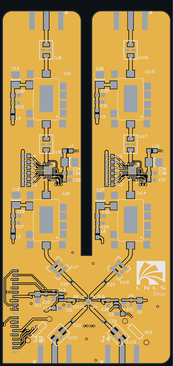
BPM RFFE (OHWR0011 R1) is an open-hardware circuit board from the CERN Open Hardware Repository, designed in Altium Designer: a 4-layer board of 50 × 105 mm with 91 components and 68 nets, published under CERN-OHL-1.1.
review 90% walked · 16 findings: 4 major · 12 minor (20 items)
Open in the interactive viewerRead the full review
Design review
Probe recorded 16 findings: 4 major · 12 minor (20 items) on this design. Each is shown here with its reasoning; the full review links every one to the pins, nets and datasheet pages it rests on.
- DuplicatePassivemajorOpen
'NetJ1_15' is pulled to 'TGND' by 2 fitted resistors (R10 (46.4), R11 (46.4))
'NetJ1_15' is pulled to 'TGND' by 2 fitted resistors: R10 (46.4), R11 (46.4) — 23R2 effective. A pull-up's value is specified, and two of them in parallel is not the value that was specified — presence checks are satisfied by either one and cannot see the pair. Which one is intended? Removing the duplicate, or recording that the parallel value is deliberate, both settle it; leaving two identical resistors on one node does not.
At NetJ1_15
- ReferencePlaneDiscontinuitymajorOpen
4 nets cross one void in the RFGND plane on BOTTOM_LAYER and the RFGND plane on MID-LAYER_2 at 1 place, the longest 1.51 mm; 4 over tracks of other nets routed inside it (fastest: NetIc13_3 at 100 ps 10-90 %, ASSUMED)
Along 'NetIc1_6' on BOTTOM_LAYER, the RFGND plane on MID-LAYER_2 has 1.51 mm under the track with copper of NetIc4_5, NetIc4_4, NetIc13_3, not a plane, at (18.89, 18.84), the same plane on both sides. No single drill's anti-pad and no landing explains it: a clearance is excused only when it holds a drill and is drawn round it, or the track ends in it on the net's own pad or via, or runs through its own via's clearance and no farther. The return current detours round the void. 4 of the crossings pass over tracks of other nets routed inside the hole on the reference layer: the plane is absent there, and those tracks stand in it. What cleared it: the hole at x 17.88..21.43, y 17.13..21.17. One decision covers the void: whether these tracks may cross it, or the plane should be filled under them. 3 of the 4 crossing(s) have a plane on the track's other side at most twice as far away as the broken one (to first order each plane beside a stripline carries a share of the return inversely proportional to its distance from the track). The rest leave most or all of the return to the break, so the finding is a warning.
- one crossing of two tracks, seen from each: 'NetIc13_3' on MID-LAYER_2 at (18.89, 19.61), 0.51 mm over copper of NetIc1_6, not a plane; other side: RFGND on MIDLAYER1, 0.32 mm from the track against 0.508 mm to BOTTOM_LAYER: 39% of the return on BOTTOM_LAYER / 'NetIc1_6' on BOTTOM_LAYER at (18.89, 18.84), 1.51 mm over copper of NetIc4_5, NetIc4_4, NetIc13_3, not a plane; other side: none: the signal layer is outermost / 'NetIc4_4' on MID-LAYER_2 at (18.89, 19.11), 0.51 mm over copper of NetIc1_6, not a plane; other side: RFGND on MIDLAYER1, 0.32 mm from the track against 0.508 mm to BOTTOM_LAYER: 39% of the return on BOTTOM_LAYER / 'NetIc4_5' on MID-LAYER_2 at (18.89, 18.56), 0.51 mm over copper of NetIc1_6, not a plane; other side: RFGND on MIDLAYER1, 0.32 mm from the track against 0.508 mm to BOTTOM_LAYER: 39% of the return on BOTTOM_LAYER
Every site is a row of this finding's evidence, keyed by net, layers and position. GET /api/odb/boards/14/reference-planes?group=void%3ARFGND%40BOTTOM_LAYER%3Ahole%2017.88%2C17.13%7C21.43%2C21.17 serves each with its own layer_image region; all of them lie in x 17.63..20.14, y 17.33..20.84 mm (board frame, Y up).
Read from the copper as drawn on the reference layer, along each track's centreline at exact breakpoints. The reference is the copper beside the track, never the layer's type or name. Whether it matters depends on each signal's edge rate, which nothing on file states for these nets: a slow static line crosses a split harmlessly, a fast edge does not.
At void:RFGND@BOTTOM_LAYER:hole 17.88,17.13|21.43,21.17
- FiducialMissingmajorOpen
FiducialMissing: 2 boards×2
2 checked by the review by Claude walker (cern session) — 2 different reasons
At bottom, top
Each finding, with its own headline
bottomThe bottom side carries 18 SMT component(s) and no fiducial was found on it
The bottom side carries 18 SMT component(s) but no fiducial was found on it — a placement machine has no optical reference to align to. Probe found no pad labelled .pad_usage=g_fiducial/l_fiducial (basis pad_usage); no single-pad, netless, undrilled component whose 0.5-3 mm round pad has a concentric solder-mask opening at least 1.5x its diameter with no other copper inside it (basis geometry); and no component whose refdes starts FID or whose part or package name contains FIDUCIAL (basis footprint-name). If your library names fiducials something Probe does not recognise, mark this benign — disposition_finding(rule='FiducialMissing', entity='bottom', status='benign', reason=…) — the name match only ever silences this check, it never asserts anything. If the side really has no fiducial, say so with status='confirmed': that answers the finding and keeps it gating release.
topThe top side carries 71 SMT component(s) and no fiducial was found on it
The top side carries 71 SMT component(s) but no fiducial was found on it — a placement machine has no optical reference to align to. Probe found no pad labelled .pad_usage=g_fiducial/l_fiducial (basis pad_usage); no single-pad, netless, undrilled component whose 0.5-3 mm round pad has a concentric solder-mask opening at least 1.5x its diameter with no other copper inside it (basis geometry); and no component whose refdes starts FID or whose part or package name contains FIDUCIAL (basis footprint-name). If your library names fiducials something Probe does not recognise, mark this benign — disposition_finding(rule='FiducialMissing', entity='top', status='benign', reason=…) — the name match only ever silences this check, it never asserts anything. If the side really has no fiducial, say so with status='confirmed': that answers the finding and keeps it gating release.
- PartLifecyclemajorOpen
PartLifecycle: 2 part numbers×2
2 Obsolete · on 11 placements
At C1, Ic2
Each finding, with its own headline
C1T495B475K016ZTE800 on 10 placements (C1, C12, C15, C16, C24, C27, C28, C36, …): the distributor catalogue reports "Obsolete" for KEMET's T495B475K016ZTE800
T495B475K016ZTE800 on 10 placements (C1, C12, C15, C16, C24, C27, C28, C36, …): the distributor catalogue reports "Obsolete" for KEMET's T495B475K016ZTE800 — a sourcing/longevity risk to confirm against the MANUFACTURER before acting. That is the maker this board's BOM names (Kemet). A distributor delisting is not the same claim as the part being unavailable; check the vendor's own lifecycle/product-change notice for the status and any named successor. Re-read the source: GET /api/odb/parts/T495B475K016ZTE800/providers (which provider said it, the maker and part number it matched, its own words, and when we asked). No approved alternate is recorded for this position.
Ic2ADT7320UCPZ-R2 on Ic2: the distributor catalogue reports "Obsolete" for Analog Devices Inc.'s ADT7320UCPZ-R2
ADT7320UCPZ-R2 on Ic2: the distributor catalogue reports "Obsolete" for Analog Devices Inc.'s ADT7320UCPZ-R2 — a sourcing/longevity risk to confirm against the MANUFACTURER before acting. That is the maker this board's BOM names (Analog Devices Inc). A distributor delisting is not the same claim as the part being unavailable; check the vendor's own lifecycle/product-change notice for the status and any named successor. Re-read the source: GET /api/odb/parts/ADT7320UCPZ-R2/providers (which provider said it, the maker and part number it matched, its own words, and when we asked). No approved alternate is recorded for this position.
RF crossbar select input Vac has no pull resistor, so the switch path is undefined when the controller does not drive it
The RF crossbar select line Vac (J1 pin 4, net NetIc1_6) has no pull resistor, so the Ic11 switch path is undefined whenever the controller does not drive it.
Where it is
``
mermaid flowchart LR J1["J1 pin 4<br/>Vac, no pull resistor"] --> B1["Ic1 TS5A3160<br/>IN pin 6"] J1 --> B2["Ic3 TS5A3160<br/>IN pin 6"] B1 -- "V1ac, R18 1k" --> SW["Ic11 RFSW6223<br/>V1 pin 3, V2 pin 7"] B2 -- "V2ac, R9 1k" --> SW``Vac drives the IN pins of both TS5A3160 buffers Ic1 and Ic3, which generate the complementary RFSW6223 controls V1 and V2. Nothing else is on that net: no pull-up or pull-down.
What the datasheet says
- "However, the IN pin must be driven high or low." (TS5A3160 datasheet, p.20)
- Floating control inputs can cause increased supply current or unknown switch selection states (p.20).
Why it matters
While the controller is unpowered, in reset, or unplugged, the crossbar can sit in either state or with both V1 and V2 part-way.
Temperature-sensor SPI (5 V domain) and attenuator serial lines (+3V domain) share J1 with no level translation
The temperature-sensor SPI (Ic2, 5 V domain) and the attenuator serial lines (Ic4/Ic13, +3V domain) share J1 with no level translation, so either a 3.3 V or a 5 V host puts one group out of specification.
The two logic domains on J1
Group Supply Input / output levels Source Ic2 ADT7320 SCLK, DIN, CS (J1 pins 19, 17, 16) +5VD VIH = 0.7 x VDD = 3.5 V ADT7320 datasheet, p.3 Ic2 ADT7320 DOUT (J1 pin 18) +5VD VOH = VDD - 0.3 V, about 4.7 V ADT7320 datasheet, p.3 Ic4, Ic13 DAT-31R5-SP+ Data, Clock, LE (J1 pins 3/2, 5, 6) +3V (through L7/L10) inputs rated to VDD + 0.3 V absolute maximum DAT-31R5-SP+ datasheet, p.2 Both groups come from the same controller header J1 with no translator on the board.
Why it matters
- A 3.3 V host does not meet the ADT7320 VIH and receives a 4.7 V DOUT.
- A 5 V host exceeds the attenuator input rating.
ADT7320 supply decoupled with 10 nF instead of the specified 0.1 uF; CT and INT pulled up but not routed anywhere
The ADT7320 Ic2 supply is decoupled with C8 10 nF instead of the specified 0.1 uF, and its CT and INT outputs are pulled up by R1/R2 but routed nowhere.
Decoupling
- Ic2 VDD (+5VD) has C8 10 nF and C7 100 pF to TGND.
- The datasheet asks for a 0.1 uF ceramic (ADT7320 datasheet, p.6).
Alert outputs
- The open-drain CT (Ic2 pin 10) and INT (Ic2 pin 9) outputs are pulled up by R1 and R2 10k to +5VD.
- Neither reaches J1 or any other part.
- The sheet carries no note saying the alerts are unused on purpose.
RF inputs are limited to about +10 dBm by the SAW filters, with no limiter and no note of the input rating
The RF inputs J3/J4 are limited to about +10 dBm by the first-stage SAW filters Ic7/Ic16 (TA1113A), with no limiter on the board and no note of the input rating.
Where it is
``
mermaid flowchart LR J3["J3 RF input"] --> F1["Ic10 LFCN-530+<br/>low-pass"] J4["J4 RF input"] --> F2["Ic12 low-pass"] F1 -- "C22" --> SW["Ic11 RFSW6223<br/>crossbar"] F2 -- "C33" --> SW SW -- "RF4, C23" --> S1["Ic7 TA1113A SAW<br/>max input 10 dBm"] SW -- "RF3, C34" --> S2["Ic16 TA1113A SAW<br/>max input 10 dBm"]``Input ratings along the chain
Stage Maximum input Source TA1113A SAW filter (Ic7, Ic16) 10 dBm TA1113A datasheet, p.2 Every later stage is rated higher: TAMP-72LN+ input +27 dBm, DAT-31R5-SP+ +24 dBm. Nothing on the board limits the level at J3/J4, and the schematic does not state the maximum input the front end tolerates.
Attenuator is not recommended for new designs and several key parts are obsolete or no longer stocked
The attenuators Ic4/Ic13 (DAT-31R5-SP+) are not recommended for new designs, and several other key parts are end of life or not carried by the distributor checked.
Part Refdes Status Source DAT-31R5-SP+ Ic4, Ic13 not recommended for new designs; replacement DAT-31R5A-SP+ DAT-31R5-SP+ datasheet, p.1 ADT7320UCPZ-R2 Ic2 end of life stored availability (Digi-Key check 2026-09-24) Kemet T495B475K016ZTE800 tantalum C1, C4, C9, C12, C15, C16, C24, C27, C28, C36 end of life stored availability RFSW6223 Ic11 not carried by the distributor checked stored availability DAT-31R5-SP+ Ic4, Ic13 not carried by the distributor checked stored availability TA1113A Ic7, Ic16 not carried by the distributor checked stored availability Schematic title block has no revision and puts the institution in the Title field; the board has no fiducials
The RFFE schematic title block has no revision and puts the institution in the Title field, and the board has no fiducials despite its fine-pitch leadless parts (Ic4, Ic13, Ic11, Ic2).
Title block
Field Content Title "Laboratorio Nacional de Luz Sincrotron - CNPEM" Number "Front-end Version 2" Revision empty Drawn By "RAB" Date the export date The PCB silkscreen names the board "RFFEv2_BD".
Fiducials
No fiducial is placed on either side, although the board carries:
- 4 mm QFN attenuators (Ic4, Ic13 DAT-31R5-SP+);
- a 3 mm QFN switch (Ic11);
- a 4 mm LFCSP sensor (Ic2).
J3 and R11 designators are printed on top of each other and neither can be read
The J3 and R11 designators are printed at the same spot on the top overlay near the RF Input-1 connector and overprint into an unreadable glyph.
The two texts sit at the lower-left board edge, where R11 (the 46.4 ohm heater resistor) is placed beside J3. They also cross two via openings in the top solder mask.
Temperature sensor sits beside the heater at the connector end, far from the SAW filters and amplifiers it is meant to stabilise
The temperature sensor Ic2 (ADT7320) sits beside the heater R10/R11 at the connector end, 20-80 mm from the SAW filters and amplifiers it is meant to stabilise, so a loop closed on it regulates the heater spot rather than the RF chain.
Where it is
Part Position on the 105 mm board Ic2 ADT7320 (bottom) about (26, 8) mm Heater R10 / R11 (top) (38, 12) / (13, 12) mm SAW filters Ic7 / Ic16 y = 28-30 mm First LNAs Ic5 / Ic14 y = 35 mm Attenuators Ic4 / Ic13 y = 57 mm Output LNAs Ic6 / Ic15 y = 71 mm Source: placement record. Ic2 lies midway between the two heater resistors.
Why it matters
A loop closed on this sensor regulates the heater spot rather than the RF chain.
Heater drive level and power are not documented; at 5 V each 46.4 ohm resistor would exceed its 0.5 W rating
The heater R10/R11 (46.4 ohm, 1/2 W each) has no documented drive level or power; driven continuously from 5 V, each resistor would dissipate 0.54 W, above its 0.5 W rating.
The numbers
Quantity Value Source Heater R10 and R11 in parallel, between the heat line (J1 pin 15, net NetJ1_15) and TGND netlist: NetJ1_15 Each resistor 46.4 ohm 1/2 W metal film, Vishay CMF55 (CMF5546R400FHEB) BOM Dissipation per resistor at a continuous 5 V 5^2 / 46.4 = 0.54 W derived Rating 0.5 W BOM Why it matters
The sheet does not say what voltage or duty drives heat. If it is driven continuously from the 5 V supplies on the same connector, each resistor runs above its rating, and the heater sits in the part of the board it is meant to warm.
Silkscreen: the large J3 legend is printed over R11's designator, so it reads as 'J3R1' next to the SMA connector
The J3 connector legend overprints the R11 reference designator on the top silkscreen, leaving R11 unreadable at assembly and rework.
On Probe's top assembly drawing (TOP_OVERLAY, rendered at about 11.7 px/mm), the bold J3 legend beside the bottom-left SMA connector and the 0.85 mm-high designator of R11 (one of the two 46.4 ohm heater resistors on net 'heat', J1.15) occupy the same spot, so the pair reads 'J3R1'. R10, the other heater resistor, is labelled clear of J4 on the right. Moving R11's designator (or the J3 legend) apart restores it.
- ConnectorDomainMixedminorOpen
J1 takes 5 different supplies off the board on one connector: +5V (5.0 V), +5VD (5.0 V), A+5V (5.0 V), C+5V (5.0 V), +3V (3.0 V)
J1 carries 5 different supplies out of the board on one connector: +5V (5.0 V) on 14, +5VD (5.0 V) on 12, A+5V (5.0 V) on 13, C+5V (5.0 V) on 8, +3V (3.0 V) on 7. Declare the intent. Two rails on one connector is ordinary in a docking or power-distribution interface and a hazard in a signal one, and the difference is not visible from the netlist — but note that adjacent contacts at different voltages are exactly what a mirrored, reversed or off-by-one cable shorts together, so the cost of getting the mating wrong is a rail collision rather than a dead signal. If this is a standard connector, declare its family (connector_family_declare) and file the standard's contact map: supplies on the contacts it assigns to power are then not reported.
At J1
- ReferencePlaneDiscontinuityminorOpen
ReferencePlaneDiscontinuity: 3 boards×3
Checked by the review, stands · Claude walker W1 (Cern session) — Checked: the void is read from the RFGND copper and stands as reported. Whether it matters depends on each crossing net's edge rate and on where its return current flows; no datasheet or app note on file sets a limit for these crossings on this RF front end, and the crossing lengths (0.69 to 4.77 mm) are short against the 530 MHz filter band. Not refutable with a citation; left for the owner.
At void:RFGND@BOTTOM_LAYER:hole 2.29,6.14|8.5,16.61, void:RFGND@BOTTOM_LAYER:hole 22.04,0.68|30.26,11.67, void:RFGND@BOTTOM_LAYER:hole 5.72,16.84|11.58,25.43
Each finding, with its own headline
void:RFGND@BOTTOM_LAYER:hole 2.29,6.14|8.5,16.61'NetIc2_4' crosses one void in the RFGND plane on BOTTOM_LAYER at 1 place, the longest 0.69 mm; 1 over tracks of other nets routed inside it (fastest: NetIc2_4 at 100 ps 10-90 %, ASSUMED)
Along 'NetIc2_4' on MID-LAYER_2, the RFGND plane on BOTTOM_LAYER has 0.69 mm under the track with copper of TGND, not a plane, at (6, 8.64), the same plane on both sides. No single drill's anti-pad and no landing explains it: a clearance is excused only when it holds a drill and is drawn round it, or the track ends in it on the net's own pad or via, or runs through its own via's clearance and no farther. The return current detours round the void. 1 of the crossings pass over tracks of other nets routed inside the hole on the reference layer: the plane is absent there, and those tracks stand in it. What cleared it: the hole at x 2.29..8.5, y 6.14..16.61. One decision covers the void: whether these tracks may cross it, or the plane should be filled under them. Every crossing has a plane on the track's other side at most twice as far away as the broken one, so at most 39% of the return meets the break and the rest follows the track on that plane (to first order each plane beside a stripline carries a share of the return inversely proportional to its distance from the track). The finding is the lower tier (info).
- 'NetIc2_4' on MID-LAYER_2 at (6, 8.64), 0.69 mm over copper of TGND, not a plane; other side: RFGND on MIDLAYER1, 0.32 mm from the track against 0.508 mm to BOTTOM_LAYER: 39% of the return on BOTTOM_LAYER
Every site is a row of this finding's evidence, keyed by net, layers and position. GET /api/odb/boards/14/reference-planes?group=void%3ARFGND%40BOTTOM_LAYER%3Ahole%202.29%2C6.14%7C8.5%2C16.61 serves each with its own layer_image region; all of them lie in x 4.63..7.3, y 7.64..9.7 mm (board frame, Y up).
Read from the copper as drawn on the reference layer, along each track's centreline at exact breakpoints. The reference is the copper beside the track, never the layer's type or name. Whether it matters depends on each signal's edge rate, which nothing on file states for these nets: a slow static line crosses a split harmlessly, a fast edge does not.
void:RFGND@BOTTOM_LAYER:hole 22.04,0.68|30.26,11.673 nets cross one void in the RFGND plane on BOTTOM_LAYER at 4 places, the longest 4.77 mm; 1 over tracks of other nets routed inside it (fastest: NetIc2_2 at 100 ps 10-90 %, ASSUMED)
Along 'NetIc2_4' on MID-LAYER_2, the RFGND plane on BOTTOM_LAYER has 4.77 mm under the track with copper of TGND, NetIc2_3, not a plane, at (24.96, 9.01), running to the end of the track. No single drill's anti-pad and no landing explains it: a clearance is excused only when it holds a drill and is drawn round it, or the track ends in it on the net's own pad or via, or runs through its own via's clearance and no farther. The return current detours round the void. 1 of the crossings pass over tracks of other nets routed inside the hole on the reference layer: the plane is absent there, and those tracks stand in it. 1 of them run ALONG the bare copper, parallel to its edges, rather than across it (the longest 0.33 mm). 4 places on 3 net(s) cross it, listed below, the longest first. What cleared it: the hole at x 22.04..30.26, y 0.68..11.67. One decision covers the void: whether these tracks may cross it, or the plane should be filled under them. Every crossing has a plane on the track's other side at most twice as far away as the broken one, so at most 39% of the return meets the break and the rest follows the track on that plane (to first order each plane beside a stripline carries a share of the return inversely proportional to its distance from the track). The finding is the lower tier (info).
- 'NetIc2_4' on MID-LAYER_2 at (24.96, 9.01), 4.77 mm over copper of TGND, NetIc2_3, not a plane, to the end of the track; other side: RFGND on MIDLAYER1, 0.32 mm from the track against 0.508 mm to BOTTOM_LAYER: 39% of the return on BOTTOM_LAYER
- 'NetIc2_3' on MID-LAYER_2 at (25.81, 10.76), 3.85 mm, running ALONG the bare copper for 0.33 mm, not across it over copper of TGND, NetIc2_1, NetIc2_2, not a plane, to the end of the track; other side: RFGND on MIDLAYER1, 0.32 mm from the track against 0.508 mm to BOTTOM_LAYER: 39% of the return on BOTTOM_LAYER
- 'NetIc2_2' on MID-LAYER_2 at (25.1, 10.88), 1 mm over copper of NetIc2_1, not a plane, to the end of the track; other side: RFGND on MIDLAYER1, 0.32 mm from the track against 0.508 mm to BOTTOM_LAYER: 39% of the return on BOTTOM_LAYER
- 'NetIc2_2' on MID-LAYER_2 at (23.58, 9.36), 0.53 mm over unnetted copper; other side: RFGND on MIDLAYER1, 0.32 mm from the track against 0.508 mm to BOTTOM_LAYER: 39% of the return on BOTTOM_LAYER
Every site is a row of this finding's evidence, keyed by net, layers and position. GET /api/odb/boards/14/reference-planes?group=void%3ARFGND%40BOTTOM_LAYER%3Ahole%2022.04%2C0.68%7C30.26%2C11.67 serves each with its own layer_image region; all of them lie in x 22.27..28.21, y 6.32..12.29 mm (board frame, Y up).
Read from the copper as drawn on the reference layer, along each track's centreline at exact breakpoints. The reference is the copper beside the track, never the layer's type or name. Whether it matters depends on each signal's edge rate, which nothing on file states for these nets: a slow static line crosses a split harmlessly, a fast edge does not.
void:RFGND@BOTTOM_LAYER:hole 5.72,16.84|11.58,25.432 nets cross one void in the RFGND plane on BOTTOM_LAYER at 4 places, the longest 4.23 mm; 3 over tracks of other nets routed inside it (fastest: NetIc4_4 at 100 ps 10-90 %, ASSUMED)
Along 'NetIc4_4' on MID-LAYER_2, the RFGND plane on BOTTOM_LAYER has 4.23 mm under the track with copper of +5V, not a plane, at (9.04, 19.11), the same plane on both sides. No single drill's anti-pad and no landing explains it: a clearance is excused only when it holds a drill and is drawn round it, or the track ends in it on the net's own pad or via, or runs through its own via's clearance and no farther. The return current detours round the void. 3 of the crossings pass over tracks of other nets routed inside the hole on the reference layer: the plane is absent there, and those tracks stand in it. 2 of them run ALONG the bare copper, parallel to its edges, rather than across it (the longest 2.91 mm). 4 places on 2 net(s) cross it, listed below, the longest first. What cleared it: the hole at x 5.72..11.58, y 16.84..25.43. One decision covers the void: whether these tracks may cross it, or the plane should be filled under them. Every crossing has a plane on the track's other side at most twice as far away as the broken one, so at most 39% of the return meets the break and the rest follows the track on that plane (to first order each plane beside a stripline carries a share of the return inversely proportional to its distance from the track). The finding is the lower tier (info).
- 'NetIc4_4' on MID-LAYER_2 at (9.04, 19.11), 4.23 mm, running ALONG the bare copper for 2.91 mm, not across it over copper of +5V, not a plane; other side: RFGND on MIDLAYER1, 0.32 mm from the track against 0.508 mm to BOTTOM_LAYER: 39% of the return on BOTTOM_LAYER
- 'NetIc4_4' on MID-LAYER_2 at (6.94, 23.49), 3.38 mm over copper of NetC9_1, not a plane; other side: RFGND on MIDLAYER1, 0.32 mm from the track against 0.508 mm to BOTTOM_LAYER: 39% of the return on BOTTOM_LAYER
- 'NetIc4_5' on MID-LAYER_2 at (6.83, 22.33), 2.34 mm over copper of NetC9_1, not a plane; other side: RFGND on MIDLAYER1, 0.32 mm from the track against 0.508 mm to BOTTOM_LAYER: 39% of the return on BOTTOM_LAYER
- 'NetIc4_5' on MID-LAYER_2 at (10.9, 18.56), 0.96 mm, running ALONG the bare copper for 0.66 mm, not across it over copper of +5V, not a plane; other side: RFGND on MIDLAYER1, 0.32 mm from the track against 0.508 mm to BOTTOM_LAYER: 39% of the return on BOTTOM_LAYER
Every site is a row of this finding's evidence, keyed by net, layers and position. GET /api/odb/boards/14/reference-planes?group=void%3ARFGND%40BOTTOM_LAYER%3Ahole%205.72%2C16.84%7C11.58%2C25.43 serves each with its own layer_image region; all of them lie in x 5.12..12.22, y 17.24..26.43 mm (board frame, Y up).
Read from the copper as drawn on the reference layer, along each track's centreline at exact breakpoints. The reference is the copper beside the track, never the layer's type or name. Whether it matters depends on each signal's edge rate, which nothing on file states for these nets: a slow static line crosses a split harmlessly, a fast edge does not.
Main parts
| Part number | Maker | Description | Where |
|---|---|---|---|
| ADT7320UCPZ-R2 | Analog Devices Inc | IC SENSR TEMP 16BIT DGTL 16LFCSP | Ic2 |
| RFSW6223 | RFMD | CrossbarSwitch | Ic11 |
| SFM-120-02-S-SH | SAMTEC | SFM-120-02-S-SH | J1 |
| DAT-31R5-SP+ | Minicircuits | Serial Digital Step Attenuator 31.5 step:0.5dB | Ic13, Ic4 |
| TA1113A | Tai-Saw Technology Co | TST_TA1113A | Ic16, Ic7 |
| TS5A3160DBVR | Texas Instruments | IC SWITCH SPDT SOT23-6 | Ic1, Ic3 |
| 132289RP | Amphenol Connex | CONN RCPT BLKHD SMA REV POL PCB | J2, J3, J4, J5 |
| TAMP-72LN+ | Minicircuits | LNA 20 dB Low Noise Figure | Ic14, Ic15, Ic5, Ic6 |
| LFCN-530+ | Minicircuits | Low Pass Filter 3dB@530MHz | Ic10, Ic12, Ic17, Ic18, Ic8, Ic9 |
| CMF5546R400FHEB | Vishay Dale | RES 46.4 OHM 1% 50PPM 1/2W | R10, R11 |
| PNM0603E1002BST5 | Vishay Thin Film | RES 10K OHM .15W 0.1% 0603 SMD | R1, R2 |
| C2012C0G1H103J/0.60 | TDK Corporation | CAP CER 10000PF 50V 5% NP0 0805 | C11, C6, C8 |
| ERJ-2GEJ102X | Panasonic Electronic Components | RES 1K OHM 1/10W 5% 0402 SMD | R18, R19, R20, R9 |
| UMK105CG101JV-F | Taiyo Yuden | CAP CER 100PF 50V 5% NP0 0402 | C10, C22, C23, C33, C34, C5 |
| C1608C0G1H102J | TDK Corporation | CAP CER 1000PF 50V 5% NP0 0603 | C14, C18, C20, C26, C3, C30, C32, C38 |
| BLM18HE601SN1D | Murata Electronics North America | FERRITE CHIP 600 OHM 800MA 0603 | L1, L10, L2, L3, L4, L5 and 4 more |
| T495B475K016ZTE800 | Kemet | CAP TANT 4.7UF 16V 10% 1411 | C1, C12, C15, C16, C24, C27 and 4 more |
| C1608C0G1H101J | TDK Corporation | CAP CER 100PF 50V 5% NP0 0603 | C13, C17, C19, C2, C21, C25 and 5 more |
| ERJ-3GEYJ103V | Panasonic - ECG | RES 10K OHM 1/10W 5% 0603 SMD | R12, R13, R14, R15, R16, R17 and 6 more |
About this design
- Design
- BPM RFFE — OHWR0011 R1
- Designed in
- Altium Designer
- Board
- 4 copper layers, 50 × 105 mm, 91 components, 68 nets
- Licence
- CERN-OHL-1.1
- Source
- https://gitlab.com/ohwr/project/bpm-rffe at commit
0ddd6b12d389 - Attribution
- CERN Open Hardware Repository, project ohwr/project/bpm-rffe (commit 0ddd6b12d38906df2484dec027f1bdcf66dadc0d, 2025-04-09). Licence: CERN-OHL-1.1. Source: https://gitlab.com/ohwr/project/bpm-rffe. This is a snapshot of the copy published on the OHWR GitLab pages (R1), not CERN's released record. CERN's source of truth is EDMS (https://edms.cern.ch), and the current release may be newer.
- Reviewed with
- Probe by E# (E-Sharp AB)