 Probe

CONV TTL BLO RTM INTERFACE TESTER
OHWR0035 · revision R1
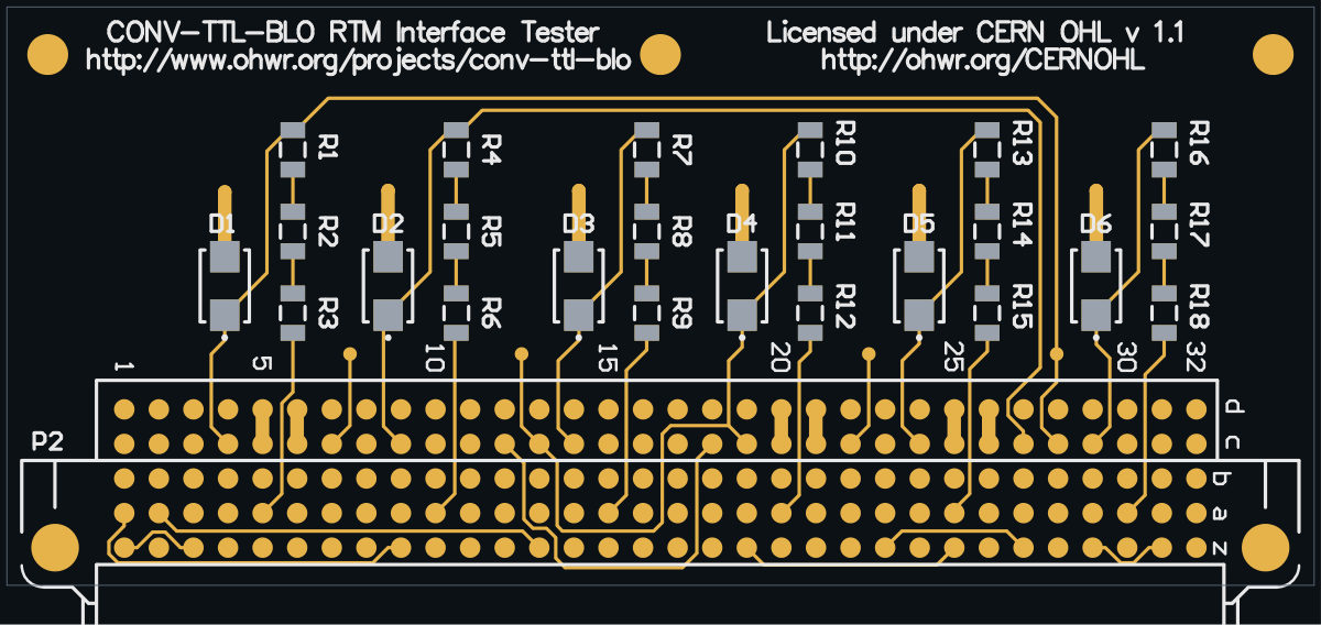
CONV TTL BLO RTM INTERFACE TESTER (OHWR0035 R1) is an open-hardware circuit board from the CERN Open Hardware Repository, designed in Altium Designer: a 2-layer board of 96 × 42.5 mm with 25 components and 32 nets, published under CERN-OHL-1.2.
review complete · 5 findings: 3 major · 2 minor (19 items)
Open in the interactive viewerRead the full review
Design review
Probe recorded 5 findings: 3 major · 2 minor (19 items) on this design. Each is shown here with its reasoning; the full review links every one to the pins, nets and datasheet pages it rests on.
- EsdProtectorPlacementmajorOpen
EsdProtectorPlacement: 12 components×12
Checked by the review, stands · Claude walker W3 (Cern session) — Checked: the via count and distance are read from the copper as stated. Placement guidance for the protector is layout practice; no datasheet requirement on file for this part sets a distance limit. Left for the owner.
At D1, D2, D3, D4, D5, D6
Each finding, with its own headline
D1D1.1 on 'BLO_C_6_P': 2 via(s) between P2.c22 and D1.1
D1 (SMBJ30CA) protects 'BLO_C_6_P' at P2.c22. Along the copper: 111.89 mm of track from the contact, 2 via(s) before it, on a 15.88 mm branch off the line; the line runs 96.02 mm on to R1.1; D1 sits 40.11 mm farther from the contact than the nearest place outside P2.
2 via(s) between P2.c22 and D1.1: the strike reaches an inner layer before it is clamped. D1.1 hangs 15.88 mm off the line (limit 1 mm, default: no datasheet figure on file): the line carries the strike past it while the clamp is reached through the branch. D1 joins the line 96.01 mm from P2.c22 on a 96.02 mm run to R1.1: nearer the far end than the contact, so the surge travels most of the line before it is clamped.
Measured on the copper the ODB states: tracks, the pads they land on, and the netlist's vias. Not a straight line between centroids.
D1D1.1 on 'BLO_C_6_P': D1.1 hangs 15.88 mm off the line (limit 1 mm, default
D1 (SMBJ30CA) protects 'BLO_C_6_P' at P2.c28. Along the copper: 98.49 mm of track from the contact, 0 via(s) before it, on a 15.88 mm branch off the line; the line runs 82.62 mm on to R1.1; D1 sits 55.15 mm farther from the contact than the nearest place outside P2.
D1.1 hangs 15.88 mm off the line (limit 1 mm, default: no datasheet figure on file): the line carries the strike past it while the clamp is reached through the branch. D1 joins the line 82.61 mm from P2.c28 on a 82.62 mm run to R1.1: nearer the far end than the contact, so the surge travels most of the line before it is clamped.
Measured on the copper the ODB states: tracks, the pads they land on, and the netlist's vias. Not a straight line between centroids.
D2D2.1 on 'BLO_C_1_P': D2.1 hangs 15.99 mm off the line (limit 1 mm, default
D2 (SMBJ30CA) protects 'BLO_C_1_P' at P2.c27. Along the copper: 84.92 mm of track from the contact, 0 via(s) before it, on a 15.99 mm branch off the line; the line runs 68.93 mm on to R4.1; D2 sits 40.8 mm farther from the contact than the nearest place outside P2.
D2.1 hangs 15.99 mm off the line (limit 1 mm, default: no datasheet figure on file): the line carries the strike past it while the clamp is reached through the branch. D2 joins the line 68.93 mm from P2.c27 on a 68.93 mm run to R4.1: nearer the far end than the contact, so the surge travels most of the line before it is clamped.
Measured on the copper the ODB states: tracks, the pads they land on, and the netlist's vias. Not a straight line between centroids.
D2D2.1 on 'BLO_C_1_P': D2 joins the line 26.57 mm from P2.c3 on a 42.56 mm run to R4.1
D2 (SMBJ30CA) protects 'BLO_C_1_P' at P2.c3. Along the copper: 26.57 mm of track from the contact, 0 via(s) before it, the line runs through its pad (flow-through); the line runs 42.56 mm on to R4.1; D2 sits 10.21 mm farther from the contact than the nearest place outside P2.
D2 joins the line 26.57 mm from P2.c3 on a 42.56 mm run to R4.1: nearer the far end than the contact, so the surge travels most of the line before it is clamped.
Measured on the copper the ODB states: tracks, the pads they land on, and the netlist's vias. Not a straight line between centroids.
D3D3.1 on 'BLO_C_2_P': D3 joins the line 43.2 mm from P2.c2 on a 59.19 mm run to R7.1
D3 (SMBJ30CA) protects 'BLO_C_2_P' at P2.c2. Along the copper: 43.2 mm of track from the contact, 0 via(s) before it, the line runs through its pad (flow-through); the line runs 59.19 mm on to R7.1; D3 sits 25.38 mm farther from the contact than the nearest place outside P2.
D3 joins the line 43.2 mm from P2.c2 on a 59.19 mm run to R7.1: nearer the far end than the contact, so the surge travels most of the line before it is clamped.
Measured on the copper the ODB states: tracks, the pads they land on, and the netlist's vias. Not a straight line between centroids.
D3D3.1 on 'BLO_C_2_P': D3 joins the line 26.88 mm from P2.c8 on a 42.87 mm run to R7.1
D3 (SMBJ30CA) protects 'BLO_C_2_P' at P2.c8. Along the copper: 26.88 mm of track from the contact, 0 via(s) before it, the line runs through its pad (flow-through); the line runs 42.87 mm on to R7.1; D3 sits 11.3 mm farther from the contact than the nearest place outside P2.
D3 joins the line 26.88 mm from P2.c8 on a 42.87 mm run to R7.1: nearer the far end than the contact, so the surge travels most of the line before it is clamped.
Measured on the copper the ODB states: tracks, the pads they land on, and the netlist's vias. Not a straight line between centroids.
D4D4.1 on 'BLO_C_3_P': D4 joins the line 34.84 mm from P2.c13 on a 50.83 mm run to R10.1
D4 (SMBJ30CA) protects 'BLO_C_3_P' at P2.c13. Along the copper: 34.84 mm of track from the contact, 0 via(s) before it, the line runs through its pad (flow-through); the line runs 50.83 mm on to R10.1; D4 sits 10.71 mm farther from the contact than the nearest place outside P2.
D4 joins the line 34.84 mm from P2.c13 on a 50.83 mm run to R10.1: nearer the far end than the contact, so the surge travels most of the line before it is clamped.
Measured on the copper the ODB states: tracks, the pads they land on, and the netlist's vias. Not a straight line between centroids.
D4D4.1 on 'BLO_C_3_P': 2 via(s) between P2.c7 and D4.1
D4 (SMBJ30CA) protects 'BLO_C_3_P' at P2.c7. Along the copper: 61.75 mm of track from the contact, 2 via(s) before it, the line runs through its pad (flow-through); the line runs 77.74 mm on to R10.1; D4 sits 24.71 mm farther from the contact than the nearest place outside P2.
2 via(s) between P2.c7 and D4.1: the strike reaches an inner layer before it is clamped. D4 joins the line 61.75 mm from P2.c7 on a 77.74 mm run to R10.1: nearer the far end than the contact, so the surge travels most of the line before it is clamped.
Measured on the copper the ODB states: tracks, the pads they land on, and the netlist's vias. Not a straight line between centroids.
D5D5.1 on 'BLO_C_4_P': D5 joins the line 56.85 mm from P2.c12 on a 72.84 mm run to R13.1
D5 (SMBJ30CA) protects 'BLO_C_4_P' at P2.c12. Along the copper: 56.85 mm of track from the contact, 0 via(s) before it, the line runs through its pad (flow-through); the line runs 72.84 mm on to R13.1; D5 sits 25 mm farther from the contact than the nearest place outside P2.
D5 joins the line 56.85 mm from P2.c12 on a 72.84 mm run to R13.1: nearer the far end than the contact, so the surge travels most of the line before it is clamped.
Measured on the copper the ODB states: tracks, the pads they land on, and the netlist's vias. Not a straight line between centroids.
D5D5.1 on 'BLO_C_4_P': D5 joins the line 26.74 mm from P2.c18 on a 42.73 mm run to R13.1
D5 (SMBJ30CA) protects 'BLO_C_4_P' at P2.c18. Along the copper: 26.74 mm of track from the contact, 0 via(s) before it, the line runs through its pad (flow-through); the line runs 42.73 mm on to R13.1; D5 sits 10.96 mm farther from the contact than the nearest place outside P2.
D5 joins the line 26.74 mm from P2.c18 on a 42.73 mm run to R13.1: nearer the far end than the contact, so the surge travels most of the line before it is clamped.
Measured on the copper the ODB states: tracks, the pads they land on, and the netlist's vias. Not a straight line between centroids.
D6D6.1 on 'BLO_C_5_P': D6 joins the line 43.05 mm from P2.c17 on a 59.04 mm run to R16.1
D6 (SMBJ30CA) protects 'BLO_C_5_P' at P2.c17. Along the copper: 43.05 mm of track from the contact, 0 via(s) before it, the line runs through its pad (flow-through); the line runs 59.04 mm on to R16.1; D6 sits 25.29 mm farther from the contact than the nearest place outside P2.
D6 joins the line 43.05 mm from P2.c17 on a 59.04 mm run to R16.1: nearer the far end than the contact, so the surge travels most of the line before it is clamped.
Measured on the copper the ODB states: tracks, the pads they land on, and the netlist's vias. Not a straight line between centroids.
D6D6.1 on 'BLO_C_5_P': D6 joins the line 26.72 mm from P2.c23 on a 42.71 mm run to R16.1
D6 (SMBJ30CA) protects 'BLO_C_5_P' at P2.c23. Along the copper: 26.72 mm of track from the contact, 0 via(s) before it, the line runs through its pad (flow-through); the line runs 42.71 mm on to R16.1; D6 sits 11.22 mm farther from the contact than the nearest place outside P2.
D6 joins the line 26.72 mm from P2.c23 on a 42.71 mm run to R16.1: nearer the far end than the contact, so the surge travels most of the line before it is clamped.
Measured on the copper the ODB states: tracks, the pads they land on, and the netlist's vias. Not a straight line between centroids.
- ReferencePlaneDiscontinuitymajorOpen
ReferencePlaneDiscontinuity: 4 boards×4
Checked by the review, stands · Claude walker W3 (Cern session) — Checked: the reference break is read from the copper as stated. Whether it matters depends on the signal's edge rate and the receiver's margin, which no datasheet or app note on file fixes for this net; the impedance step and reflection figures are Probe's model, and the thresholds are its starting values. Layout practice, not a datasheet requirement. Left for the owner.
At void:BLO_C_1_N@BOTTOM_LAYER:hole 10.23,6.92|42.57,12.8, void:BLO_C_1_N@BOTTOM_LAYER:hole 24.52,16.32|38.48,17.68, void:BLO_C_1_N@BOTTOM_LAYER:hole 48.33,6.92|80.67,12.8, void:BLO_C_1_N@BOTTOM_LAYER:hole 62.62,16.32|77.78,17.68
Each finding, with its own headline
void:BLO_C_1_N@BOTTOM_LAYER:hole 10.23,6.92|42.57,12.85 nets cross one void in the BLO_C_1_N plane on BOTTOM_LAYER at 6 places, the longest 3.11 mm; 6 over tracks of other nets routed inside it (fastest: BLO_C_1_P at 100 ps 10-90 %, ASSUMED)
Along 'BLO_IN_1_P' on TOP_LAYER, the BLO_C_1_N plane on BOTTOM_LAYER has 3.11 mm under the track with copper of BLO_C_1_P, BLO_C_1_N, BLO_C_2_P, not a plane, at (20.19, 10.39), the same plane on both sides. No single drill's anti-pad and no landing explains it: a clearance is excused only when it holds a drill and is drawn round it, or the track ends in it on the net's own pad or via, or runs through its own via's clearance and no farther. The return current detours round the void. 6 of the crossings pass over tracks of other nets routed inside the hole on the reference layer: the plane is absent there, and those tracks stand in it. 6 places on 5 net(s) cross it, listed below, the longest first. What cleared it: the hole at x 10.23..42.57, y 6.92..12.8. One decision covers the void: whether these tracks may cross it, or the plane should be filled under them. No crossing has a plane on the track's other side, so the whole return meets the break.
- 'BLO_IN_1_P' on TOP_LAYER at (20.19, 10.39), 3.11 mm over copper of BLO_C_1_P, BLO_C_1_N, BLO_C_2_P, not a plane; other side: none: the signal layer is outermost
- 'BLO_C_3_P' on TOP_LAYER at (24.72, 11.25), 1.4 mm over copper of BLO_C_2_P, not a plane, to the end of the track; other side: none: the signal layer is outermost
- 'BLO_C_1_P' on TOP_LAYER at (28.08, 11.25), 1.39 mm over copper of BLO_C_2_P, not a plane, to the end of the track; other side: none: the signal layer is outermost
- 'BLO_C_6_P' on TOP_LAYER at (15.38, 11.25), 1.38 mm over copper of BLO_C_2_P, not a plane, to the end of the track; other side: none: the signal layer is outermost
- 'BLO_C_3_P' on TOP_LAYER at (38.01, 11.49), 0.73 mm over copper of BLO_C_2_P, not a plane; other side: none: the signal layer is outermost
- 'BLO_IN_2_P' on TOP_LAYER at (32.89, 11.7), 0.61 mm over copper of BLO_C_2_P, not a plane; other side: none: the signal layer is outermost
Every site is a row of this finding's evidence, keyed by net, layers and position. GET /api/odb/boards/36/reference-planes?group=void%3ABLO_C_1_N%40BOTTOM_LAYER%3Ahole%2010.23%2C6.92%7C42.57%2C12.8 serves each with its own layer_image region; all of them lie in x 14..39.09, y 7.9..13 mm (board frame, Y up).
Read from the copper as drawn on the reference layer, along each track's centreline at exact breakpoints. The reference is the copper beside the track, never the layer's type or name. Whether it matters depends on each signal's edge rate, which nothing on file states for these nets: a slow static line crosses a split harmlessly, a fast edge does not.
void:BLO_C_1_N@BOTTOM_LAYER:hole 24.52,16.32|38.48,17.682 nets cross one void in the BLO_C_1_N plane on BOTTOM_LAYER at 2 places, the longest 0.61 mm; 2 over tracks of other nets routed inside it (fastest: BLO_C_1_P at 100 ps 10-90 %, ASSUMED)
Along 'BLO_C_1_P' on TOP_LAYER, the BLO_C_1_N plane on BOTTOM_LAYER has 0.61 mm under the track with copper of BLO_C_3_P, not a plane, at (27.65, 17), the same plane on both sides. No single drill's anti-pad and no landing explains it: a clearance is excused only when it holds a drill and is drawn round it, or the track ends in it on the net's own pad or via, or runs through its own via's clearance and no farther. The return current detours round the void. 2 of the crossings pass over tracks of other nets routed inside the hole on the reference layer: the plane is absent there, and those tracks stand in it. 2 places on 2 net(s) cross it, listed below, the longest first. What cleared it: the hole at x 24.52..38.48, y 16.32..17.68. One decision covers the void: whether these tracks may cross it, or the plane should be filled under them. No crossing has a plane on the track's other side, so the whole return meets the break.
- 'BLO_C_1_P' on TOP_LAYER at (27.65, 17), 0.61 mm over copper of BLO_C_3_P, not a plane; other side: none: the signal layer is outermost
- 'BLO_IN_2_P' on TOP_LAYER at (32.89, 17), 0.61 mm over copper of BLO_C_3_P, not a plane; other side: none: the signal layer is outermost
Every site is a row of this finding's evidence, keyed by net, layers and position. GET /api/odb/boards/36/reference-planes?group=void%3ABLO_C_1_N%40BOTTOM_LAYER%3Ahole%2024.52%2C16.32%7C38.48%2C17.68 serves each with its own layer_image region; all of them lie in x 26.65..33.89, y 15.7..18.3 mm (board frame, Y up).
Read from the copper as drawn on the reference layer, along each track's centreline at exact breakpoints. The reference is the copper beside the track, never the layer's type or name. Whether it matters depends on each signal's edge rate, which nothing on file states for these nets: a slow static line crosses a split harmlessly, a fast edge does not.
void:BLO_C_1_N@BOTTOM_LAYER:hole 48.33,6.92|80.67,12.86 nets cross one void in the BLO_C_1_N plane on BOTTOM_LAYER at 7 places, the longest 4.25 mm; 7 over tracks of other nets routed inside it (fastest: BLO_C_1_P at 100 ps 10-90 %, ASSUMED)
Along 'BLO_C_3_P' on TOP_LAYER, the BLO_C_1_N plane on BOTTOM_LAYER has 4.25 mm under the track with copper of BLO_C_5_P, not a plane, at (51.72, 11.73), running to the end of the track. No single drill's anti-pad and no landing explains it: a clearance is excused only when it holds a drill and is drawn round it, or the track ends in it on the net's own pad or via, or runs through its own via's clearance and no farther. The return current detours round the void. 7 of the crossings pass over tracks of other nets routed inside the hole on the reference layer: the plane is absent there, and those tracks stand in it. 1 of them run ALONG the bare copper, parallel to its edges, rather than across it (the longest 2.51 mm). 7 places on 6 net(s) cross it, listed below, the longest first. What cleared it: the hole at x 48.33..80.67, y 6.92..12.8. One decision covers the void: whether these tracks may cross it, or the plane should be filled under them. No crossing has a plane on the track's other side, so the whole return meets the break.
- 'BLO_C_3_P' on TOP_LAYER at (51.72, 11.73), 4.25 mm, running ALONG the bare copper for 2.51 mm, not across it over copper of BLO_C_5_P, not a plane, to the end of the track; other side: none: the signal layer is outermost
- 'BLO_IN_4_P' on TOP_LAYER at (58.2, 10.39), 3.11 mm over copper of BLO_C_4_P, BLO_C_1_N, BLO_C_5_P, not a plane; other side: none: the signal layer is outermost
- 'BLO_C_6_P' on TOP_LAYER at (62.82, 11.25), 1.4 mm over copper of BLO_C_5_P, not a plane, to the end of the track; other side: none: the signal layer is outermost
- 'BLO_C_4_P' on TOP_LAYER at (66.18, 11.25), 1.39 mm over copper of BLO_C_5_P, not a plane, to the end of the track; other side: none: the signal layer is outermost
- 'BLO_C_1_P' on TOP_LAYER at (74.29, 11.7), 1.14 mm over copper of BLO_C_5_P, not a plane, to the end of the track; other side: none: the signal layer is outermost
- 'BLO_C_6_P' on TOP_LAYER at (76.11, 11.49), 0.69 mm over copper of BLO_C_5_P, not a plane; other side: none: the signal layer is outermost
- 'BLO_IN_5_P' on TOP_LAYER at (70.71, 11.7), 0.61 mm over copper of BLO_C_5_P, not a plane; other side: none: the signal layer is outermost
Every site is a row of this finding's evidence, keyed by net, layers and position. GET /api/odb/boards/36/reference-planes?group=void%3ABLO_C_1_N%40BOTTOM_LAYER%3Ahole%2048.33%2C6.92%7C80.67%2C12.8 serves each with its own layer_image region; all of them lie in x 49.17..77.19, y 7.9..13 mm (board frame, Y up).
Read from the copper as drawn on the reference layer, along each track's centreline at exact breakpoints. The reference is the copper beside the track, never the layer's type or name. Whether it matters depends on each signal's edge rate, which nothing on file states for these nets: a slow static line crosses a split harmlessly, a fast edge does not.
void:BLO_C_1_N@BOTTOM_LAYER:hole 62.62,16.32|77.78,17.683 nets cross one void in the BLO_C_1_N plane on BOTTOM_LAYER at 3 places, the longest 0.86 mm; 3 over tracks of other nets routed inside it (fastest: BLO_C_1_P at 100 ps 10-90 %, ASSUMED)
Along 'BLO_C_4_P' on TOP_LAYER, the BLO_C_1_N plane on BOTTOM_LAYER has 0.86 mm under the track with copper of BLO_C_6_P, not a plane, at (66.25, 17), the same plane on both sides. No single drill's anti-pad and no landing explains it: a clearance is excused only when it holds a drill and is drawn round it, or the track ends in it on the net's own pad or via, or runs through its own via's clearance and no farther. The return current detours round the void. 3 of the crossings pass over tracks of other nets routed inside the hole on the reference layer: the plane is absent there, and those tracks stand in it. 3 places on 3 net(s) cross it, listed below, the longest first. What cleared it: the hole at x 62.62..77.78, y 16.32..17.68. One decision covers the void: whether these tracks may cross it, or the plane should be filled under them. No crossing has a plane on the track's other side, so the whole return meets the break.
- 'BLO_C_4_P' on TOP_LAYER at (66.25, 17), 0.86 mm over copper of BLO_C_6_P, not a plane; other side: none: the signal layer is outermost
- 'BLO_IN_5_P' on TOP_LAYER at (71.8, 17), 0.81 mm over copper of BLO_C_6_P, not a plane; other side: none: the signal layer is outermost
- 'BLO_C_1_P' on TOP_LAYER at (75.9, 17), 0.61 mm over copper of BLO_C_6_P, not a plane; other side: none: the signal layer is outermost
Every site is a row of this finding's evidence, keyed by net, layers and position. GET /api/odb/boards/36/reference-planes?group=void%3ABLO_C_1_N%40BOTTOM_LAYER%3Ahole%2062.62%2C16.32%7C77.78%2C17.68 serves each with its own layer_image region; all of them lie in x 64.95..76.9, y 15.7..18.3 mm (board frame, Y up).
Read from the copper as drawn on the reference layer, along each track's centreline at exact breakpoints. The reference is the copper beside the track, never the layer's type or name. Whether it matters depends on each signal's edge rate, which nothing on file states for these nets: a slow static line crosses a split harmlessly, a fast edge does not.
- FiducialMissingmajorOpen
The top side carries 24 SMT component(s) and no fiducial was found on it
The top side carries 24 SMT component(s) but no fiducial was found on it — a placement machine has no optical reference to align to. Probe found no pad labelled .pad_usage=g_fiducial/l_fiducial (basis pad_usage); no single-pad, netless, undrilled component whose 0.5-3 mm round pad has a concentric solder-mask opening at least 1.5x its diameter with no other copper inside it (basis geometry); and no component whose refdes starts FID or whose part or package name contains FIDUCIAL (basis footprint-name). If your library names fiducials something Probe does not recognise, mark this benign — disposition_finding(rule='FiducialMissing', entity='top', status='benign', reason=…) — the name match only ever silences this check, it never asserts anything. If the side really has no fiducial, say so with status='confirmed': that answers the finding and keeps it gating release.
At top
Each TVS D1-D6 returns to ground through a single thermally relieved via
Each TVS D1-D6 (SMBJ30CA) returns to ground through a single thermally relieved via, which puts via and spoke inductance in series with the 48.4 V clamp during fast edges.
Where it is
- Ground side: each diode's pin 2 is on net BLO_C_1_N, the board ground (shared with 83 P2 ground contacts). The pad leaves on a short top-layer stub to one via, and that via joins the bottom-layer ground pour through four thermal-relief spokes. Six such vias, one per TVS.
- No second via, and no direct top-layer connection from the TVS ground pad to the P2 ground contacts.
- Protected side: the node (P2 c-row pins to the 3 x 51 Ω chain) is routed directly to the TVS cathode pad; e.g. D1 pin 1 is on BLO_C_6_P with P2.c4, P2.c22, P2.c28 and R1.1. D2-D6 follow the same pattern.
Why it matters
A clamp only works as well as its return. One via with thermal spokes adds on the order of 1 nH plus spoke inductance, and during a fast edge that voltage appears in series with the clamp. On a passive bench tester for 24 V class pulses this is a small effect, hence minor.
Suggested fix: add a second via, or remove the thermal relief on these six vias.
Schematic title block leaves document number, revision, checker and sheet number as placeholders
The schematic title block leaves the document number, revision, checker and sheet number as placeholders.
The single sheet (RTM_Interface_Tester.SchDoc) fills in the board name "PTS RTM Interface Tester", the project "Blocking Pulse Repeater PTS", the designer (Theodor-Adrian Stana) and the date 4/24/2013. These fields print
*:- Document number
- Check by
- Sheet (
* of *) - Rev
Without a revision on the drawing a reader cannot tie a built tester to this schematic, and the fabrication files carry no revision either. Documentation only; it does not affect function.
Main parts
| Part number | Maker | Description | Where |
|---|---|---|---|
| 02 04 160 1101 | HARTING | Connector 160zabcd Female (5x32) | P2 |
| SMBJ30CA | FAIRCHILD SEMICONDUCTOR | Transient Voltage Suppressor Diode (Bi-Directional) | D1, D2, D3, D4, D5, D6 |
| R1206_51R_0.1%_0.25W_25PPM | GENERIC | Resistor - 0.1% | R1, R10, R11, R12, R13, R14 and 12 more |
About this design
- Design
- CONV TTL BLO RTM INTERFACE TESTER — OHWR0035 R1
- Designed in
- Altium Designer
- Board
- 2 copper layers, 96 × 42.5 mm, 25 components, 32 nets
- Licence
- CERN-OHL-1.2
- Source
- https://gitlab.com/ohwr/project/conv-ttl-blo-hw at commit
498b1ff562ff - Attribution
- CERN Open Hardware Repository, project ohwr/project/conv-ttl-blo-hw (commit 498b1ff562ff10fb00f56bebc7e7f603573110a5, 2025-04-09). Licence: CERN-OHL-1.2. Source: https://gitlab.com/ohwr/project/conv-ttl-blo-hw. This is a snapshot of the copy published on the OHWR GitLab pages (R1), not CERN's released record. CERN's source of truth is EDMS (https://edms.cern.ch), and the current release may be newer.
- Reviewed with
- Probe by E# (E-Sharp AB)