 Probe

CONV TTL RS485 TESTER
OHWR0036 · revision R1
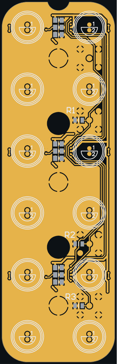
CONV TTL RS485 TESTER (OHWR0036 R1) is an open-hardware circuit board from the CERN Open Hardware Repository, designed in Altium Designer: a 2-layer board of 31.2 × 99.7 mm with 34 components and 36 nets, published under CERN-OHL-1.2.
review 96% walked · 8 findings: 2 major · 6 minor (12 items)
Open in the interactive viewerRead the full review
Design review
Probe recorded 8 findings: 2 major · 6 minor (12 items) on this design. Each is shown here with its reasoning; the full review links every one to the pins, nets and datasheet pages it rests on.
- ReferencePlaneDiscontinuitymajorOpen
ReferencePlaneDiscontinuity: 5 boards×5
Checked by the review, stands · Claude walker W3 (Cern session) — Checked: the reference break is read from the copper as stated. Whether it matters depends on the signal's edge rate and the receiver's margin, which no datasheet or app note on file fixes for this net; the impedance step and reflection figures are Probe's model, and the thresholds are its starting values. Layout practice, not a datasheet requirement. Left for the owner.
At void:GND@TOP_LAYER:hole 1.48,22.6|2.56,25.18, void:GND@TOP_LAYER:hole 1.48,56.89|2.56,59.47, void:GND@TOP_LAYER:hole 1.48,91.18|2.56,93.76, void:GND@TOP_LAYER:hole 11.64,14.51|30.06,96.61, void:GND@TOP_LAYER:hole 11.64,53.57|20.27,69.28
Each finding, with its own headline
void:GND@TOP_LAYER:hole 1.48,22.6|2.56,25.18'O33_N' crosses one void in the GND plane on TOP_LAYER at 1 place, the longest 0.79 mm; 1 over tracks of other nets routed inside it (fastest: O33_N at 100 ps 10-90 %, ASSUMED)
Along 'O33_N' on BOTTOM_LAYER, the GND plane on TOP_LAYER has 0.79 mm under the track with copper of O33_P, not a plane, at (2.27, 23.8), the same plane on both sides. No single drill's anti-pad and no landing explains it: a clearance is excused only when it holds a drill and is drawn round it, or the track ends in it on the net's own pad or via, or runs through its own via's clearance and no farther. The return current detours round the void. 1 of the crossings pass over tracks of other nets routed inside the hole on the reference layer: the plane is absent there, and those tracks stand in it. What cleared it: the hole at x 1.48..2.56, y 22.6..25.18. One decision covers the void: whether these tracks may cross it, or the plane should be filled under them. No crossing has a plane on the track's other side, so the whole return meets the break.
- 'O33_N' on BOTTOM_LAYER at (2.27, 23.8), 0.79 mm over copper of O33_P, not a plane; other side: none: the signal layer is outermost
Every site is a row of this finding's evidence, keyed by net, layers and position. GET /api/odb/boards/37/reference-planes?group=void%3AGND%40TOP_LAYER%3Ahole%201.48%2C22.6%7C2.56%2C25.18 serves each with its own layer_image region; all of them lie in x 0.63..3.41, y 22.76..24.8 mm (board frame, Y up).
Read from the copper as drawn on the reference layer, along each track's centreline at exact breakpoints. The reference is the copper beside the track, never the layer's type or name. Whether it matters depends on each signal's edge rate, which nothing on file states for these nets: a slow static line crosses a split harmlessly, a fast edge does not.
void:GND@TOP_LAYER:hole 1.48,56.89|2.56,59.47'O23_N' crosses one void in the GND plane on TOP_LAYER at 1 place, the longest 0.79 mm; 1 over tracks of other nets routed inside it (fastest: O23_N at 100 ps 10-90 %, ASSUMED)
Along 'O23_N' on BOTTOM_LAYER, the GND plane on TOP_LAYER has 0.79 mm under the track with copper of O23_P, not a plane, at (2.27, 58.09), the same plane on both sides. No single drill's anti-pad and no landing explains it: a clearance is excused only when it holds a drill and is drawn round it, or the track ends in it on the net's own pad or via, or runs through its own via's clearance and no farther. The return current detours round the void. 1 of the crossings pass over tracks of other nets routed inside the hole on the reference layer: the plane is absent there, and those tracks stand in it. What cleared it: the hole at x 1.48..2.56, y 56.89..59.47. One decision covers the void: whether these tracks may cross it, or the plane should be filled under them. No crossing has a plane on the track's other side, so the whole return meets the break.
- 'O23_N' on BOTTOM_LAYER at (2.27, 58.09), 0.79 mm over copper of O23_P, not a plane; other side: none: the signal layer is outermost
Every site is a row of this finding's evidence, keyed by net, layers and position. GET /api/odb/boards/37/reference-planes?group=void%3AGND%40TOP_LAYER%3Ahole%201.48%2C56.89%7C2.56%2C59.47 serves each with its own layer_image region; all of them lie in x 0.63..3.41, y 57.05..59.09 mm (board frame, Y up).
Read from the copper as drawn on the reference layer, along each track's centreline at exact breakpoints. The reference is the copper beside the track, never the layer's type or name. Whether it matters depends on each signal's edge rate, which nothing on file states for these nets: a slow static line crosses a split harmlessly, a fast edge does not.
void:GND@TOP_LAYER:hole 1.48,91.18|2.56,93.76'O13_N' crosses one void in the GND plane on TOP_LAYER at 1 place, the longest 0.79 mm; 1 over tracks of other nets routed inside it (fastest: O13_N at 100 ps 10-90 %, ASSUMED)
Along 'O13_N' on BOTTOM_LAYER, the GND plane on TOP_LAYER has 0.79 mm under the track with copper of O13_P, not a plane, at (2.27, 92.38), the same plane on both sides. No single drill's anti-pad and no landing explains it: a clearance is excused only when it holds a drill and is drawn round it, or the track ends in it on the net's own pad or via, or runs through its own via's clearance and no farther. The return current detours round the void. 1 of the crossings pass over tracks of other nets routed inside the hole on the reference layer: the plane is absent there, and those tracks stand in it. What cleared it: the hole at x 1.48..2.56, y 91.18..93.76. One decision covers the void: whether these tracks may cross it, or the plane should be filled under them. No crossing has a plane on the track's other side, so the whole return meets the break.
- 'O13_N' on BOTTOM_LAYER at (2.27, 92.38), 0.79 mm over copper of O13_P, not a plane; other side: none: the signal layer is outermost
Every site is a row of this finding's evidence, keyed by net, layers and position. GET /api/odb/boards/37/reference-planes?group=void%3AGND%40TOP_LAYER%3Ahole%201.48%2C91.18%7C2.56%2C93.76 serves each with its own layer_image region; all of them lie in x 0.63..3.41, y 91.34..93.38 mm (board frame, Y up).
Read from the copper as drawn on the reference layer, along each track's centreline at exact breakpoints. The reference is the copper beside the track, never the layer's type or name. Whether it matters depends on each signal's edge rate, which nothing on file states for these nets: a slow static line crosses a split harmlessly, a fast edge does not.
void:GND@TOP_LAYER:hole 11.64,14.51|30.06,96.6116 nets cross one void in the GND plane on TOP_LAYER at 34 places, the longest 16.2 mm; 29 over tracks of other nets routed inside it (fastest: O11_N at 100 ps 10-90 %, ASSUMED)
Along 'O22_N' on BOTTOM_LAYER, the GND plane on TOP_LAYER has 16.2 mm under the track with copper of EN, S0, S1, P3V, O22_P, not a plane, at (23.05, 56.58), the same plane on both sides. No single drill's anti-pad and no landing explains it: a clearance is excused only when it holds a drill and is drawn round it, or the track ends in it on the net's own pad or via, or runs through its own via's clearance and no farther. The return current detours round the void. 29 of the crossings pass over tracks of other nets routed inside the hole on the reference layer: the plane is absent there, and those tracks stand in it. 7 of them run ALONG the bare copper, parallel to its edges, rather than across it (the longest 9.88 mm). 34 places on 16 net(s) cross it, listed below, the longest first. What cleared it: the hole at x 11.64..30.06, y 14.51..96.61. One decision covers the void: whether these tracks may cross it, or the plane should be filled under them. No crossing has a plane on the track's other side, so the whole return meets the break.
- 'O22_N' on BOTTOM_LAYER at (23.05, 56.58), 16.2 mm, running ALONG the bare copper for 9.88 mm, not across it over copper of EN, S0, S1, P3V, O22_P, not a plane; other side: none: the signal layer is outermost
- 'O12_N' on BOTTOM_LAYER at (23.05, 90.87), 11.45 mm, running ALONG the bare copper for 6.51 mm, not across it over copper of EN, S0, S1, P3V, O12_P, not a plane; other side: none: the signal layer is outermost
- 'O22_P' on BOTTOM_LAYER at (23.28, 60.3), 11.27 mm, running ALONG the bare copper for 6.24 mm, not across it over copper of EN, S0, S1, P3V, not a plane, to the end of the track; other side: none: the signal layer is outermost
- 'O12_P' on BOTTOM_LAYER at (23.28, 94.59), 11.26 mm, running ALONG the bare copper for 6.34 mm, not across it over copper of P3V, not a plane, to the end of the track; other side: none: the signal layer is outermost
- 'EN' on BOTTOM_LAYER at (20.18, 58.35), 6.51 mm, running ALONG the bare copper for 0.56 mm, not across it over copper of S0, S1, P3V, not a plane; other side: none: the signal layer is outermost
- 'EN' on BOTTOM_LAYER at (20.18, 92.79), 6.51 mm, running ALONG the bare copper for 1.39 mm, not across it over copper of P3V, S0, S1, not a plane; other side: none: the signal layer is outermost
- 'O21_P' on BOTTOM_LAYER at (22.45, 58.69), 6.5 mm over copper of EN, S0, P3V, S1, not a plane, to the end of the track; other side: none: the signal layer is outermost
- 'O21_N' on BOTTOM_LAYER at (22.45, 58.18), 6.38 mm over copper of EN, S0, S1, not a plane, to the end of the track; other side: none: the signal layer is outermost
- 'O11_N' on BOTTOM_LAYER at (22.45, 92.47), 6.21 mm, running ALONG the bare copper for 2.56 mm, not across it over copper of EN, S0, S1, not a plane, to the end of the track; other side: none: the signal layer is outermost
- 'O12_N' on BOTTOM_LAYER at (29.21, 78.82), 3.78 mm over copper of EN, S0, S1, P3V, not a plane; other side: none: the signal layer is outermost
- 'O12_P' on BOTTOM_LAYER at (29.21, 79.53), 3.78 mm over copper of EN, S0, S1, P3V, not a plane; other side: none: the signal layer is outermost
- 'O22_N' on BOTTOM_LAYER at (29.15, 44.47), 3.65 mm over copper of EN, S0, S1, P3V, not a plane; other side: none: the signal layer is outermost
- and 22 more
Every site is a row of this finding's evidence, keyed by net, layers and position. GET /api/odb/boards/37/reference-planes?group=void%3AGND%40TOP_LAYER%3Ahole%2011.64%2C14.51%7C30.06%2C96.61 serves each with its own layer_image region; all of them lie in x 12.9..30.86, y 19.14..97.59 mm (board frame, Y up).
Read from the copper as drawn on the reference layer, along each track's centreline at exact breakpoints. The reference is the copper beside the track, never the layer's type or name. Whether it matters depends on each signal's edge rate, which nothing on file states for these nets: a slow static line crosses a split harmlessly, a fast edge does not.
void:GND@TOP_LAYER:hole 11.64,53.57|20.27,69.285 nets cross one void in the GND plane on TOP_LAYER at 7 places, the longest 1.73 mm; 5 over tracks of other nets routed inside it (fastest: O21_P at 100 ps 10-90 %, ASSUMED)
Along 'O21_P' on BOTTOM_LAYER, the GND plane on TOP_LAYER has 1.73 mm under the track with copper of GND, P3V, not a plane, at (16.66, 61.91), running to the end of the track. No single drill's anti-pad and no landing explains it: a clearance is excused only when it holds a drill and is drawn round it, or the track ends in it on the net's own pad or via, or runs through its own via's clearance and no farther. The return current detours round the void. 5 of the crossings pass over tracks of other nets routed inside the hole on the reference layer: the plane is absent there, and those tracks stand in it. 7 places on 5 net(s) cross it, listed below, the longest first. What cleared it: the hole at x 11.64..20.27, y 53.57..69.28. One decision covers the void: whether these tracks may cross it, or the plane should be filled under them. No crossing has a plane on the track's other side, so the whole return meets the break.
- 'O21_P' on BOTTOM_LAYER at (16.66, 61.91), 1.73 mm over copper of GND, P3V, not a plane, to the end of the track; other side: none: the signal layer is outermost
- 'O22_P' on BOTTOM_LAYER at (17.07, 62.42), 1.45 mm over copper of P3V, not a plane; other side: none: the signal layer is outermost
- 'O23_P' on BOTTOM_LAYER at (14.63, 62.16), 1.36 mm over copper of P3V, not a plane, to the end of the track; other side: none: the signal layer is outermost
- 'O22_P' on BOTTOM_LAYER at (15.93, 62.16), 1.22 mm over copper of P3V, not a plane; other side: none: the signal layer is outermost
- 'O23_N' on BOTTOM_LAYER at (14.43, 54.62), 1.13 mm over copper of P3V, not a plane; other side: none: the signal layer is outermost
- 'O23_N' on BOTTOM_LAYER at (14.95, 55.87), 0.87 mm over copper of NetC6_1, not a plane, to the end of the track; other side: none: the signal layer is outermost
- 'EN' on BOTTOM_LAYER at (17.2, 60.92), 0.46 mm over copper of GND, not a plane, to the end of the track; other side: none: the signal layer is outermost
Every site is a row of this finding's evidence, keyed by net, layers and position. GET /api/odb/boards/37/reference-planes?group=void%3AGND%40TOP_LAYER%3Ahole%2011.64%2C53.57%7C20.27%2C69.28 serves each with its own layer_image region; all of them lie in x 12.9..18.79, y 53.43..63.42 mm (board frame, Y up).
Read from the copper as drawn on the reference layer, along each track's centreline at exact breakpoints. The reference is the copper beside the track, never the layer's type or name. Whether it matters depends on each signal's edge rate, which nothing on file states for these nets: a slow static line crosses a split harmlessly, a fast edge does not.
- FiducialMissingmajorOpen
The top side carries 12 SMT component(s) and no fiducial was found on it
The top side carries 12 SMT component(s) but no fiducial was found on it — a placement machine has no optical reference to align to. Probe found no pad labelled .pad_usage=g_fiducial/l_fiducial (basis pad_usage); no single-pad, netless, undrilled component whose 0.5-3 mm round pad has a concentric solder-mask opening at least 1.5x its diameter with no other copper inside it (basis geometry); and no component whose refdes starts FID or whose part or package name contains FIDUCIAL (basis footprint-name). If your library names fiducials something Probe does not recognise, mark this benign — disposition_finding(rule='FiducialMissing', entity='top', status='benign', reason=…) — the name match only ever silences this check, it never asserts anything. If the side really has no fiducial, say so with status='confirmed': that answers the finding and keeps it gating release.
At top
Mux control inputs EN, S0, S1 come straight off LEMO sockets, rated only to VDD + 0.3 V
The MAX14778 control inputs EN, S0 and S1 come straight off LEMO sockets J2, J3 and J4 with no series resistor, while the supply P3V arrives separately on J1, so a driven control cable with J1 unpowered overdrives inputs rated only to VDD + 0.3 V.
Where it is
Net Socket Pull-down MAX14778 pins (U1, U2, U3) EN J2 pin 1 R1 10k 10 (ENA), 16 (ENB) S0 J3 pin 1 R2 10k 11 (SA0), 15 (SB0) S1 J4 pin 1 R3 10k 12 (SA1), 14 (SB1) The supply P3V enters only on J1 pin 1.
What the datasheet says
ENA, ENB, SA_, SB_: -0.3 V to VDD + 0.3 V absolute maximum (MAX14778 datasheet, p.2).
Why it matters
If a control cable is driven while J1 is unplugged or not yet powered, or from 5 V logic onto the 3.3 V supply, the inputs are over their rating and the source back-powers P3V through the input clamps. There is no series resistor to limit that current.
MAX14778 charge-pump outputs VP/VN bypassed with 1 uF where the datasheet specifies 100 nF
The MAX14778 charge-pump outputs VP/VN are bypassed with 1 uF (C2, C3, C5, C6, C8, C9) where the datasheet specifies 100 nF, which lowers the unpowered input dv/dt limit tenfold and slows charge-pump start-up.
Where it is
Mux VP capacitor VN capacitor U1 C2 C3 U2 C5 C6 U3 C8 C9 All are 1 uF 50 V X7R 0805.
The numbers
Quantity Value Source Specified VP / VN bypass 100 nF 50 V ceramic each MAX14778 datasheet, p.10 Input dv/dt limit when unpowered stated for 100 nF MAX14778 datasheet, p.12 dv/dt that reaches the same current with 1 uF one tenth, about 0.3 V/us derived Why it matters
When the board is unpowered, signals applied to the A_, B_ and COM pins charge the VP/VN capacitors through internal diodes, and that charging current must stay under the 300 mA diode rating. With ten times the capacitance the same current is reached at one tenth of the dv/dt. The charge pumps also take longer to reach +35 V and -27 V at power-up.
Input sockets I1-I3 land directly on the mux COM pins; the 510 ohm series resistors are drawn but not on this board
The input sockets I1-I3 land directly on the MAX14778 COM pins; the 510 ohm series resistors R4-R9 are drawn but live on another assembly, not on this board.
Where it is
``
mermaid flowchart LR I1["I1 pins 1 / 2<br/>input socket"] -- "I1_P / I1_N, no series R" --> U1["U1 MAX14778<br/>ACOM pin 5 / BCOM pin 1"] SUP["support board<br/>R4-R9 510 ohm, per note"] -.- I1``- The schematic draws R4-R9 510 ohm between each input socket (I1-I3, pins 1 and 2) and the ACOM/BCOM pins, with the note "Resistors placed between this board and support board".
- They are not in the BOM or the layout. I1 pin 1 connects straight to U1 pin 5 (ACOM) and I1 pin 2 to U1 pin 1 (BCOM), and likewise for I2/U2 and I3/U3.
Why it matters
The datasheet gives the A_ and B_ pins extended ESD protection (MAX14778 datasheet, p.12); the COM pins have only the basic protection. So the only series impedance between the input cables and the COM pins lives on another assembly.
Title block does not identify this board or its revision; BOM tolerance disagrees with the drawing; no fiducials
The title block does not identify this board or its revision, the R1-R3 tolerance on the drawing disagrees with the BOM, and the board has no fiducials.
Title block
Field Content Document "RTM Interface Tester" Project/Equipment "Pulse converter PTS" Rev "-" Check.by "*" Drawing date 10/10/2014 The repository and PCB are the CONV TTL RS485 tester.
Tolerance
R1-R3 carry "1%" on the symbol, but the library part and BOM description say 0.1 %.
Fiducials
The board has no fiducials, with three 5 mm TQFN-20 parts (U1, U2, U3 MAX14778) on the bottom side.
Decoupling capacitors C1-C9 carry no reference designators on the silkscreen
The nine decoupling capacitors C1-C9 carry no reference designators on either silkscreen.
- The top overlay labels R1, R2 and R3.
- The bottom overlay labels U1-U3, J1-J4 and every LEMO socket.
- C1-C9 (0805) sit on the top side in three groups of three opposite U1, U2 and U3, with no designator printed on either side.
- FiducialMissingminorOpen
The bottom side carries 3 SMT component(s) and no fiducial was found on it
The bottom side carries 3 SMT component(s) but no fiducial was found on it — a placement machine has no optical reference to align to. Probe found no pad labelled .pad_usage=g_fiducial/l_fiducial (basis pad_usage); no single-pad, netless, undrilled component whose 0.5-3 mm round pad has a concentric solder-mask opening at least 1.5x its diameter with no other copper inside it (basis geometry); and no component whose refdes starts FID or whose part or package name contains FIDUCIAL (basis footprint-name). If your library names fiducials something Probe does not recognise, mark this benign — disposition_finding(rule='FiducialMissing', entity='bottom', status='benign', reason=…) — the name match only ever silences this check, it never asserts anything. If the side really has no fiducial, say so with status='confirmed': that answers the finding and keeps it gating release. Graded minor: the side carries only 3 SMT part(s) (at most 5), which a placement machine can usually align on their own pads; a fine-pitch part among them would still want one.
At bottom
Main parts
| Part number | Maker | Description | Where |
|---|---|---|---|
| MAX14778ETP+ | Maxim dual +/-25 V 4:1 analog multiplexer, channel 1: ACOM = I1_P, BCOM = I1_N | U1, U2, U3 | |
| EPA.00.250.NTN | LEMO 00 coaxial fixed socket; P3V supply in (centre), shell GND | J1, J2, J3, J4 | |
| FAA.0S.302.CLA | LEMO FAA.0S.302.CLA: S series size 0S fixed plug, 2 low-voltage contacts, snap-on, nut fixing (LEMO datasheet p1); pin 1 = _P, pin 2 = _N | I1, I2, I3, O11, O12, O13 and 6 more |
About this design
- Design
- CONV TTL RS485 TESTER — OHWR0036 R1
- Designed in
- Altium Designer
- Board
- 2 copper layers, 31.2 × 99.7 mm, 34 components, 36 nets
- Licence
- CERN-OHL-1.2
- Source
- https://gitlab.com/ohwr/project/conv-ttl-rs485-hw at commit
e2dd3dc0ecf5 - Attribution
- CERN Open Hardware Repository, project ohwr/project/conv-ttl-rs485-hw (commit e2dd3dc0ecf534a43464bf6ede930563ac44a03d, 2025-04-09). Licence: CERN-OHL-1.2. Source: https://gitlab.com/ohwr/project/conv-ttl-rs485-hw. This is a snapshot of the copy published on the OHWR GitLab pages (R1), not CERN's released record. CERN's source of truth is EDMS (https://edms.cern.ch), and the current release may be newer.
- Reviewed with
- Probe by E# (E-Sharp AB)