 Probe

DIOT CRATE POWER BACKPLANE
OHWR0085 · revision R4
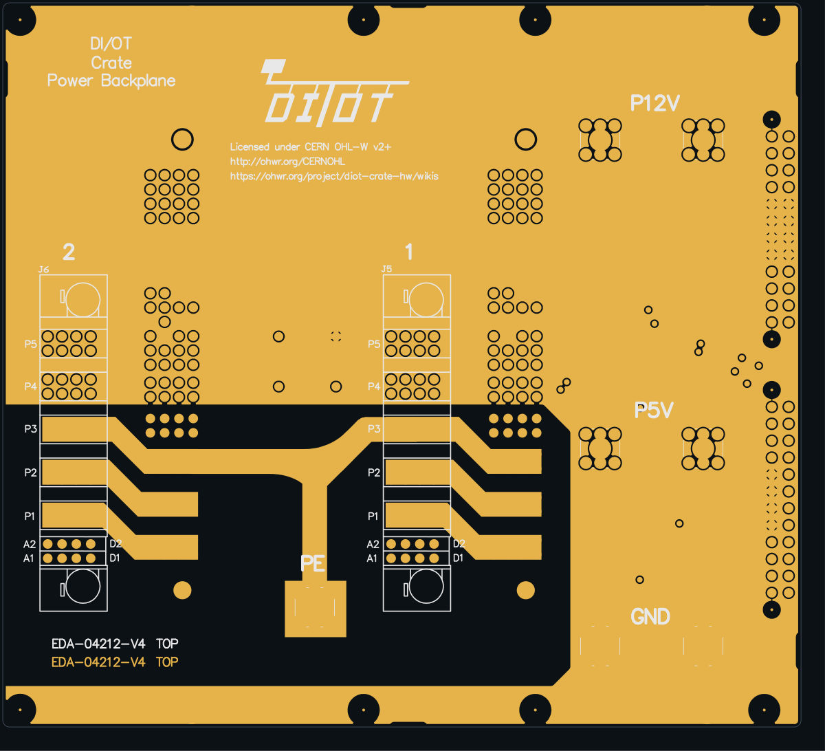
DIOT CRATE POWER BACKPLANE (OHWR0085 R4) is an open-hardware circuit board from its public repository, designed in Altium Designer: a 4-layer board of 141.7 × 128.5 mm with 30 components and 28 nets, published under CERN-OHL-W-2.0.
review complete · 1 item need the designer's input · 3 findings: 2 major · 1 minor (14 items)
Open in the interactive viewerRead the full review
Design review
Probe recorded 3 findings: 2 major · 1 minor (14 items) on this design. Each is shown here with its reasoning; the full review links every one to the pins, nets and datasheet pages it rests on.
- AssemblySeammajorOpen
AssemblySeam: 6 nets×6
e.g. “Nothing sources DC_RTN1 (OHWR-DIOT-CRATE-V3)”
At DC_RTN1, DC_RTN2, L1, L2, N1, N2
Each finding, with its own headline
DC_RTN1Nothing sources DC_RTN1 (OHWR-DIOT-CRATE-V3)
Every board this rail reaches receives it (PBP DC_RTN1, ACDC0 VRECT, PSU0 P24V), no declared member sources it, and it leaves the build through no other connector.
Found by the seam review of OHWR-DIOT-CRATE-V3 build 2 (M9-rail-direction, across seam:16, seam:18), where this board sits as PBP. On the assembly it is STALE: decided refuted by Claude interconnect reviewer (Cern session): Refuted for the real crate. DC_RTN1 carries VRECT (+24 V) of the RaToPUSv2 AC/DC stage seated as ACDC0, produced on that board by the D1 (DST2080C) / D2 (DSTF3060CR) full-wave bridge from the 2x 18 V secondaries of its off-board toroid TR1 (Multicomp MCTA160/18), which enter on its J3 (CERN schematic EDA-04862-V2-0 sheet 1). The transformer is now seated as declared member TR0 (supply, no copper). No MCTA160/18 datasheet or pinout is on file, so no connection diagram is declared and the engine cannot see it source; in addition the bridge rule does not admit VRECT (CERN BUG-072). The polarity of this feed against spec Table 3 is raised separately in OBS-581.
DC_RTN2Nothing sources DC_RTN2 (OHWR-DIOT-CRATE-V3)
Every board this rail reaches receives it (PBP DC_RTN2, ACDC1 VRECT, PSU1 P24V), no declared member sources it, and it leaves the build through no other connector.
Found by the seam review of OHWR-DIOT-CRATE-V3 build 2 (M9-rail-direction, across seam:17, seam:19), where this board sits as PBP. On the assembly it is STALE: decided refuted by Claude interconnect reviewer (Cern session): Refuted for the real crate. DC_RTN2 carries VRECT (+24 V) of the RaToPUSv2 AC/DC stage seated as ACDC1, produced on that board by the D1 (DST2080C) / D2 (DSTF3060CR) full-wave bridge from the 2x 18 V secondaries of its off-board toroid TR1 (Multicomp MCTA160/18), which enter on its J3 (CERN schematic EDA-04862-V2-0 sheet 1). The transformer is now seated as declared member TR1 (supply, no copper). No MCTA160/18 datasheet or pinout is on file, so no connection diagram is declared and the engine cannot see it source; in addition the bridge rule does not admit VRECT (CERN BUG-072). The polarity of this feed against spec Table 3 is raised separately in OBS-581.
L1Nothing sources L1 (OHWR-DIOT-CRATE-V3)
Every board this rail reaches receives it (PBP L1), no declared member sources it, and it leaves the build through no other connector.
Found by the seam review of OHWR-DIOT-CRATE-V3 build 2 (M9-rail-direction, across seam:16, seam:18), where this board sits as PBP. On the assembly it is STALE: decided refuted by Claude interconnect reviewer (Cern session): Refuted: in build 2 nothing takes L1 from the power backplane. The RaToPUSv2 AC/DC stage gets its mains on its own inlet and the DC/DC stage leaves P1/P2 open, so L1 is an unused pass-through between the back-panel slot and the front slot (both ends are open pads on the RaToPUS stages). There is nothing for anything to source. In build 1 these lines carry the AC Input module's switched mains to the Hartmann PSU.
L2Nothing sources L2 (OHWR-DIOT-CRATE-V3)
Every board this rail reaches receives it (PBP L2), no declared member sources it, and it leaves the build through no other connector.
Found by the seam review of OHWR-DIOT-CRATE-V3 build 2 (M9-rail-direction, across seam:17, seam:19), where this board sits as PBP. On the assembly it is STALE: decided refuted by Claude interconnect reviewer (Cern session): Refuted: in build 2 nothing takes L2 from the power backplane. The RaToPUSv2 AC/DC stage gets its mains on its own inlet and the DC/DC stage leaves P1/P2 open, so L2 is an unused pass-through between the back-panel slot and the front slot (both ends are open pads on the RaToPUS stages). There is nothing for anything to source. In build 1 these lines carry the AC Input module's switched mains to the Hartmann PSU.
N1Nothing sources N1 (OHWR-DIOT-CRATE-V3)
Every board this rail reaches receives it (PBP N1), no declared member sources it, and it leaves the build through no other connector.
Found by the seam review of OHWR-DIOT-CRATE-V3 build 2 (M9-rail-direction, across seam:16, seam:18), where this board sits as PBP. On the assembly it is STALE: decided refuted by Claude interconnect reviewer (Cern session): Refuted: in build 2 nothing takes N1 from the power backplane. The RaToPUSv2 AC/DC stage gets its mains on its own inlet and the DC/DC stage leaves P1/P2 open, so N1 is an unused pass-through between the back-panel slot and the front slot (both ends are open pads on the RaToPUS stages). There is nothing for anything to source. In build 1 these lines carry the AC Input module's switched mains to the Hartmann PSU.
N2Nothing sources N2 (OHWR-DIOT-CRATE-V3)
Every board this rail reaches receives it (PBP N2), no declared member sources it, and it leaves the build through no other connector.
Found by the seam review of OHWR-DIOT-CRATE-V3 build 2 (M9-rail-direction, across seam:17, seam:19), where this board sits as PBP. On the assembly it is STALE: decided refuted by Claude interconnect reviewer (Cern session): Refuted: in build 2 nothing takes N2 from the power backplane. The RaToPUSv2 AC/DC stage gets its mains on its own inlet and the DC/DC stage leaves P1/P2 open, so N2 is an unused pass-through between the back-panel slot and the front slot (both ends are open pads on the RaToPUS stages). There is nothing for anything to source. In build 1 these lines carry the AC Input module's switched mains to the Hartmann PSU.
- ReferencePlaneDiscontinuitymajorOpen
ReferencePlaneDiscontinuity: 6 boards×6
Checked by the review, stands · Claude walker V2 (cern-01 session) — Post-0.529.0 verify, 6 warning-tier findings on the power backplane's L3/BOTTOM_LAYER routing: PWRFAIL_N and P_IO0 along the DC_RTN1/P5V split, P_PRES0 and BNC_RST+ reference changes GND to P5V, CUR_SHARE1 across the DC_IN1/DC_RTN1 split (0.91 mm), PS_ON_N over two P5V pull-backs (1.3-1.5 mm), and BNC_RST+/M_SDA/P_IO1 along cut-outs round other tracks. These are static or slow PSU control and status lines (power-fail, presence, PS_ON, PSU I/O), I2C management, a front-panel reset passthrough, and a DC current-share line. None is a clock, a high-speed pair or a converter control line. The rule's 100 ps edge is assumed; no edge is on file. The finding stands as layout practice; no observation is warranted.
At along@BOTTOM_LAYER:DC_RTN1|P5V, refchange:GND|P5V, split@BOTTOM_LAYER:DC_IN1|DC_RTN1, void:P5V@BOTTOM_LAYER:126.25,147.13, void:P5V@BOTTOM_LAYER:167.84,147.17, void:routed@BOTTOM_LAYER|L3
Each finding, with its own headline
along@BOTTOM_LAYER:DC_RTN1|P5V2 nets run ALONG the split between the DC_RTN1 and P5V planes on BOTTOM_LAYER at 2 places, the longest 15.11 mm; the impedance there is not said (fastest: PWRFAIL_N at 100 ps 10-90 %, ASSUMED)
On BOTTOM_LAYER the DC_RTN1 and P5V planes part, and 2 nets run down the slot between them at 2 place(s), rather than across it. This is not a crossing: the return still follows the track, in the plane on its other side and in the slot's edges, so it does not detour. What changes is the track's own impedance. With the plane gone from under it on this side for that length, its field reaches further, to the slot's edges and to the next plane beyond, so its capacitance falls and its impedance rises; every edge travelling down it is partly reflected where it enters the stretch and again where it leaves, by (Z2 - Z1)/(Z2 + Z1). The longer the stretch against the edge's rise, the more of the edge sees the full step. A crossing is generally the worse fault; a mismatch is not free. At 2 place(s) the impedance cannot be said: no plane lies on the track's other side or past the split layer, so the field along the slot has nothing to end on. No place stays within 10 %, the tolerance controlled impedance is commonly built to (the stackup states none), so the finding is a warning. One decision covers the split line's slot: whether these tracks may run down it, or should be moved over solid plane.
- 'PWRFAIL_N' on L3 at (169.32, 145.06), 17.67 mm, running ALONG the split for 15.11 mm, not across it, impedance not said: no plane lies on the track's other side or past the split layer, so the field along the slot has nothing to end on; other side: no plane on L2
- 'P_IO0' on L3 at (164.01, 142.52), 16.9 mm, running ALONG the split for 8.94 mm, not across it, impedance not said: no plane lies on the track's other side or past the split layer, so the field along the slot has nothing to end on; other side: no plane on L2
Every site is a row of this finding's evidence, keyed by net, layers and position. GET /api/odb/boards/89/reference-planes?group=along%40BOTTOM_LAYER%3ADC_RTN1%7CP5V serves each with its own layer_image region; all of them lie in x 158.32..179.17, y 140.26..146.06 mm (board frame, Y up).
Read from the copper as drawn on the reference layer, along each track's centreline at exact breakpoints. The reference is the copper beside the track, never the layer's type or name. Whether it matters depends on each signal's edge rate, which nothing on file states for these nets: a slow static line crosses a split harmlessly, a fast edge does not.
refchange:GND|P5V2 nets change reference between GND and P5V at 2 vias, none with a reference that continues across (fastest: P_PRES0 at 100 ps 10-90 %, ASSUMED)
At 2 via(s), on 2 net(s), the signal leaves a layer referenced by one of GND and P5V for a layer referenced by the other, and no plane references both layers. Different nets: no via can carry the return across; only decoupling between the two planes near the via can. The capacitor carrying the return across was measured at each via, at the knee of the crossing net's edge against 50 ohm assumed: 2 with none. 2 of them at an ASSUMED edge (no edge on file for the net): state one (net_timing_state) and it is re-read. One decision covers the pair: whether GND and P5V are decoupled to each other near these vias. A via whose layers have more references than these two is a site of each pair it joins. None is partial: at every one, no reference continues across the via.
- 'P_PRES0' at (196.54, 113.1), L2 -> L3: GND on TOP_LAYER to P5V on BOTTOM_LAYER; pure, no reference continues across; stitching none, 24.6 mm of track past the via on L3: At the 5 GHz knee of a 100 ps edge (100 ps 10-90 %, assumed: no edge is on file for the net) no capacitor carries the return; only the planes do. GND and P5V are not a thin pair (at most 0.2 mm), so their own capacitance does not carry the return. To serve it, change layers across the same plane, or move the signal to a layer referenced to ground. None.
- 'BNC_RST+' at (189.61, 133.63), L2 -> L3: GND on TOP_LAYER to P5V on BOTTOM_LAYER; pure, no reference continues across; stitching none, 23.4 mm of track past the via on L3: At the 5 GHz knee of a 100 ps edge (20 ns 10-90 %, assumed: no edge is on file for the net) no capacitor carries the return; only the planes do. GND and P5V are not a thin pair (at most 0.2 mm), so their own capacitance does not carry the return. To serve it, change layers across the same plane, or move the signal to a layer referenced to ground. None.
Every site is a row of this finding's evidence, keyed by net, layers and position. GET /api/odb/boards/89/reference-planes?group=refchange%3AGND%7CP5V serves each with its own layer_image region; all of them lie in x 187.61..198.54, y 111.1..135.63 mm (board frame, Y up).
The reference on each layer is the first plane the track meets leaving the via, anti-pads and the net's own copper skipped. Whether it matters depends on each signal's edge rate, which nothing on file states for these nets: a slow static line crosses a split harmlessly, a fast edge does not.
split@BOTTOM_LAYER:DC_IN1|DC_RTN1'CUR_SHARE1' crosses the split between the DC_IN1 and DC_RTN1 planes on BOTTOM_LAYER at 1 place, with no plane on the track's other side (fastest: CUR_SHARE1 at 100 ps 10-90 %, ASSUMED)
On BOTTOM_LAYER the DC_IN1 and DC_RTN1 planes part, and 'CUR_SHARE1' crosses from one to the other at 1 place(s). The return current cannot follow a track across; it detours to wherever the two planes are joined (a stitching capacitor, or the source), and the loop it opens radiates and couples. One decision covers the boundary: whether it is stitched near these crossings, or the nets crossing it are slow enough not to care. Tracks that run ALONG this split, down the slot rather than across it, are a finding of their own: theirs is an impedance step, not a detour. At 0 of the 1 crossing(s) the track's other neighbour carries a plane, which the return can use there. No crossing has a plane on the track's other side, so the whole return meets the break.
- 'CUR_SHARE1' on L3 at (158.56, 137.39), 0.91 mm; other side: no plane on L2
Every site is a row of this finding's evidence, keyed by net, layers and position. GET /api/odb/boards/89/reference-planes?group=split%40BOTTOM_LAYER%3ADC_IN1%7CDC_RTN1 serves each with its own layer_image region; all of them lie in x 157.11..160.02, y 136.39..138.39 mm (board frame, Y up).
Read from the copper as drawn on the reference layer, along each track's centreline at exact breakpoints. The reference is the copper beside the track, never the layer's type or name. Whether it matters depends on each signal's edge rate, which nothing on file states for these nets: a slow static line crosses a split harmlessly, a fast edge does not.
void:P5V@BOTTOM_LAYER:126.25,147.13'PS_ON_N' crosses where the outline of the P5V plane on BOTTOM_LAYER is drawn back, at 1 place, the longest 1.51 mm (fastest: PS_ON_N at 100 ps 10-90 %, ASSUMED)
Along 'PS_ON_N' on L3, the P5V plane on BOTTOM_LAYER has 1.51 mm under the track with no copper, at (126.25, 147.13), the same plane on both sides. No single drill's anti-pad and no landing explains it: a clearance is excused only when it holds a drill and is drawn round it, or the track ends in it on the net's own pad or via, or runs through its own via's clearance and no farther. The return current detours round the void. No hole cleared it: the outline of the pour at x 101.54..215.21, y 99.3..157.14 is drawn back there. One decision covers the void: whether these tracks may cross it, or the plane should be filled under them. No crossing has a plane on the track's other side, so the whole return meets the break.
- 'PS_ON_N' on L3 at (126.25, 147.13), 1.51 mm over no copper; other side: no plane on L2
Every site is a row of this finding's evidence, keyed by net, layers and position. GET /api/odb/boards/89/reference-planes?group=void%3AP5V%40BOTTOM_LAYER%3A126.25%2C147.13 serves each with its own layer_image region; all of them lie in x 123.32..127.52, y 145.3..148.4 mm (board frame, Y up).
Read from the copper as drawn on the reference layer, along each track's centreline at exact breakpoints. The reference is the copper beside the track, never the layer's type or name. Whether it matters depends on each signal's edge rate, which nothing on file states for these nets: a slow static line crosses a split harmlessly, a fast edge does not.
void:P5V@BOTTOM_LAYER:167.84,147.17'PS_ON_N' crosses where the outline of the P5V plane on BOTTOM_LAYER is drawn back, at 1 place, the longest 1.29 mm (fastest: PS_ON_N at 100 ps 10-90 %, ASSUMED)
Along 'PS_ON_N' on L3, the P5V plane on BOTTOM_LAYER has 1.29 mm under the track with no copper, at (167.84, 147.17), the same plane on both sides. No single drill's anti-pad and no landing explains it: a clearance is excused only when it holds a drill and is drawn round it, or the track ends in it on the net's own pad or via, or runs through its own via's clearance and no farther. The return current detours round the void. No hole cleared it: the outline of the pour at x 101.54..215.21, y 99.3..157.14 is drawn back there. One decision covers the void: whether these tracks may cross it, or the plane should be filled under them. No crossing has a plane on the track's other side, so the whole return meets the break.
- 'PS_ON_N' on L3 at (167.84, 147.17), 1.29 mm over no copper; other side: no plane on L2
Every site is a row of this finding's evidence, keyed by net, layers and position. GET /api/odb/boards/89/reference-planes?group=void%3AP5V%40BOTTOM_LAYER%3A167.84%2C147.17 serves each with its own layer_image region; all of them lie in x 166.61..170.73, y 145.34..148.4 mm (board frame, Y up).
Read from the copper as drawn on the reference layer, along each track's centreline at exact breakpoints. The reference is the copper beside the track, never the layer's type or name. Whether it matters depends on each signal's edge rate, which nothing on file states for these nets: a slow static line crosses a split harmlessly, a fast edge does not.
void:routed@BOTTOM_LAYER|L3Tracks on BOTTOM_LAYER and L3 cross each other at 2 places, each layer the other's reference with its pour cleared round its own tracks, the longest 42.06 mm; 5 run ALONG the cut round another net's track (fastest: PS_ON_N at 100 ps 10-90 %, ASSUMED)
BOTTOM_LAYER and L3 each carry a pour and routed tracks, and each is the other's nearest reference. Wherever a track on one crosses a track on the other, the pour under it is cleared round that other track, so for the width of the cut the return has no plane under it and detours round the cut. 2 place(s) on 7 net(s), 1 of them seen from both tracks (each counted once). 5 of the crossings run ALONG the cut round another net's track rather than across it, parallel to its edges (the longest 24.34 mm): over or right beside that track, broadside to it as well as off the plane. One decision covers the layer pair: whether these layers may take a pour their own tracks cut as the reference, or the routing or the stackup should give the tracks a plane that is not cut where they cross. No crossing has a plane on the track's other side, so the whole return meets the break.
- one crossing of two tracks, seen from each: 'BNC_RST+' on L3 at (205.42, 133.72), 7.98 mm over copper of M_SCL, M_SDA, P_PRES1, PWRFAIL_N, P12V_Sense, not a plane, to the end of the track; other side: no plane on L2 / 'M_SDA' on BOTTOM_LAYER at (207.95, 128.85), 42.06 mm, running ALONG the bare copper for 7.25 mm, not across it over copper of PS_ON_N, PWRFAIL_N, P_IO0, P_IO1, PE, BNC_RST+, P_PRES0, not a plane, to the end of the track; other side: none: the signal layer is outermost / 'PS_ON_N' on L3 at (200.33, 147.6), 39.02 mm, running ALONG the bare copper for 24.34 mm, not across it over copper of M_SCL, M_SDA, RTN_Sense, P12V_Sense, not a plane, to the end of the track; other side: no plane on L2 / 'PWRFAIL_N' on L3 at (198.52, 145.06), 7.06 mm over copper of M_SCL, M_SDA, not a plane, to the end of the track; other side: no plane on L2 / 'P_IO0' on L3 at (207.29, 141.25), 15.84 mm, running ALONG the bare copper for 6.76 mm, not across it over copper of M_SCL, M_SDA, P_PRES1, PWRFAIL_N, not a plane, to the end of the track; other side: no plane on L2 / 'P_IO1' on L3 at (199.07, 140.09), 8.14 mm over copper of M_SCL, M_SDA, P_PRES1, PWRFAIL_N, not a plane, to the end of the track; other side: no plane on L2 / 'P_PRES0' on L3 at (210.79, 117.05), 12.26 mm, running ALONG the bare copper for 1.96 mm, not across it over copper of M_SCL, M_SDA, P_PRES1, not a plane, to the end of the track; other side: no plane on L2
- 'P_IO1' on L3 at (170.21, 139.8), 11.91 mm, running ALONG the bare copper for 8.02 mm, not across it over copper of CUR_SHARE1, P_PRES0, not a plane, to the end of the track; other side: no plane on L2
Every site is a row of this finding's evidence, keyed by net, layers and position. GET /api/odb/boards/89/reference-planes?group=void%3Arouted%40BOTTOM_LAYER%7CL3 serves each with its own layer_image region; all of them lie in x 165.13..216.95, y 114.8..149.2 mm (board frame, Y up).
Read from the copper as drawn on the reference layer, along each track's centreline at exact breakpoints. The reference is the copper beside the track, never the layer's type or name. Whether it matters depends on each signal's edge rate, which nothing on file states for these nets: a slow static line crosses a split harmlessly, a fast edge does not.
- ConnectorDomainMixedminorOpen
ConnectorDomainMixed: 2 components×2
2 checked by the review by Claude walker E (Cern session) — 2 different reasons
At J1, J2
Each finding, with its own headline
J1J1 takes 2 different supplies off the board on one connector: P12V (12 V), P5V (5 V)
J1 carries 2 different supplies out of the board on one connector: P12V (12 V) on P8/P9, P5V (5 V) on C6/D6. Declare the intent. Two rails on one connector is ordinary in a docking or power-distribution interface and a hazard in a signal one, and the difference is not visible from the netlist — but note that adjacent contacts at different voltages are exactly what a mirrored, reversed or off-by-one cable shorts together, so the cost of getting the mating wrong is a rail collision rather than a dead signal. If this is a standard connector, declare its family (connector_family_declare) and file the standard's contact map: supplies on the contacts it assigns to power are then not reported.
J2J2 takes 2 different supplies off the board on one connector: P12V (12 V), P5V (5 V)
J2 carries 2 different supplies out of the board on one connector: P12V (12 V) on P8/P9, P5V (5 V) on C6/D6. Declare the intent. Two rails on one connector is ordinary in a docking or power-distribution interface and a hazard in a signal one, and the difference is not visible from the netlist — but note that adjacent contacts at different voltages are exactly what a mirrored, reversed or off-by-one cable shorts together, so the cost of getting the mating wrong is a rail collision rather than a dead signal. If this is a standard connector, declare its family (connector_family_declare) and file the standard's contact map: supplies on the contacts it assigns to power are then not reported.
Main parts
| Part number | Maker | Description | Where |
|---|---|---|---|
| 7461057 | WURTH | Bush | BUSH7 |
| RMF_0R_JUMPER_1016-630X250 | GENERIC | Resistor | R1 |
| 44769-2402 | MOLEX | Connector 24 Female | J3, J4 |
| 51940-581 | AMPHENOL | Thru-Hole, Lead 3.43mm, PowerBlade Vertical Power Connector 3ACP 2P 24S 4DCP Contacts | J5, J6 |
| 51940-650 | AMPHENOL | Thru-Hole, Lead 3.43mm, PowerBlade Vertical Power Connector 3ACP 2P 24S 4DCP Contacts | J1, J2 |
| Use only in PCB | Fiducial Target | FTG1, FTG2, FTG3 |
About this design
- Design
- DIOT CRATE POWER BACKPLANE — OHWR0085 R4
- Designed in
- Altium Designer
- Board
- 4 copper layers, 141.7 × 128.5 mm, 30 components, 28 nets
- Licence
- CERN-OHL-W-2.0
- Source
- https://edms.cern.ch/item/EDA-04212-V4-0/0 at commit
EDMS EDA-042 - Attribution
- CERN EDMS item EDA-04212-V4-0 'DI/OT Crate - Power Backplane': document 3086360 v.1, retrieved 2026-10-18T12:59:22Z. CERN EDA-04212 V4, DI/OT Crate - Power Backplane. Copyright CERN 2019, 2024. Licence: CERN OHL-W v2.0+. Project: https://gitlab.com/ohwr/project/diot-crate-hw
- Reviewed with
- Probe by E# (E-Sharp AB)