 Probe

DIOT FMC CARRIER
OHWR0090 · revision R2
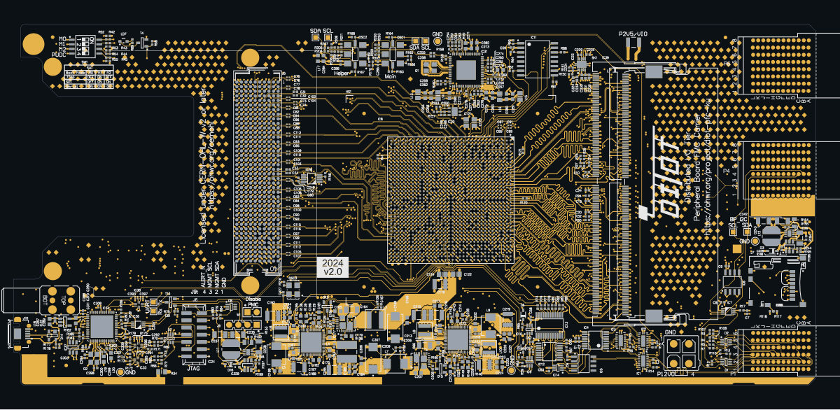
DIOT FMC CARRIER (OHWR0090 R2) is an open-hardware circuit board from its public repository, designed in Altium Designer: a 12-layer board of 222 × 100 mm with 692 components and 854 nets, published under CERN-OHL-W-2.0.
review 85% walked · 16 findings: 1 blocker · 6 major · 9 minor (46 items)
Open in the interactive viewerRead the full review
Design review
Probe recorded 16 findings: 1 blocker · 6 major · 9 minor (46 items) on this design. Each is shown here with its reasoning; the full review links every one to the pins, nets and datasheet pages it rests on.
- PowerGroundShortblockerOpen
'GND' carries a power pin (IC21.22) and a ground pin (IC23.11)
Net 'GND' connects a power pin (IC21.22) and a ground pin (IC23.11).
At GND
- DecapOrdermajorOpen
DecapOrder: 8 findings (5 pins, 3 components)×8
Checked by the review, stands · Claude walker X1 (cern-01 session) — Checked at verify (0.531.4; these findings appeared once BUG-086 gave the generic capacitors their kind). The order stands as drawn: on IC8 (XCKU035) P0V95/P2V5/VCCO pins, the 47 uF bulk parts (C125/C126 etc.) sit nearer the balls than the 4.7 uF parts (C127-C159, 2.7-4.8 mm). That runs against UG583 v1.29 p311's concentric-ring order ('followed by the smallest-value decoupling capacitors, then the larger-value'). But UG583's own quantitative placement criterion on the same page, within one-fortieth of a wavelength at the capacitor's mounted resonant frequency, is met with large margin by a 4.7 uF part at <=5 mm (a mounted resonance of a few MHz puts lambda/40 in the tens of cm). No PDN target is stated on these rails, so no impedance consequence can be judged. IC5 (ADN4661) and IC12 (SN74CB3T3257) pins with C1 1 nF at about 4.3 mm: their datasheets on file state no ordering or distance. Probe's 5 mm radius and 10x step are layout heuristics, not datasheet requirements. Left open for the owner; no observation proposed.
At IC12.16, IC5.1, IC8, IC8.A16, IC8.AK29, IC8.R24
Each finding, with its own headline
IC12.16IC12 supply pin 16 on 'P3V3': the smallest capacitor C1 sits 4.3 mm away, behind C60 at 1.8 mm
IC12 supply pin 16 on 'P3V3': the smallest capacitor C1 sits 4.3 mm away, behind C60 at 1.8 mm. IC12.16: the smallest value, C1 (1 nF), is 4.3 mm from the pin and C60 (100 nF) 1.8 mm: the high-frequency part sits behind more inductance than the bulk part, which needs it least. Swap them, or bring the smallest value to the pin: it serves the fastest current and is the one the loop inductance defeats. Distances are pad centre to pin centre in the board plane. The 5 mm radius, the 10x value step and the 1 mm / 1.5x tie tolerance are Probe's starting values.
IC5.1IC5 supply pin 1 on 'P3V3': the smallest capacitor C1 sits 4.2 mm away, behind C6 at 1.8 mm
IC5 supply pin 1 on 'P3V3': the smallest capacitor C1 sits 4.2 mm away, behind C6 at 1.8 mm. IC5.1: the smallest value, C1 (1 nF), is 4.2 mm from the pin and C6 (100 nF) 1.8 mm: the high-frequency part sits behind more inductance than the bulk part, which needs it least. Swap them, or bring the smallest value to the pin: it serves the fastest current and is the one the loop inductance defeats. Distances are pad centre to pin centre in the board plane. The 5 mm radius, the 10x value step and the 1 mm / 1.5x tie tolerance are Probe's starting values.
IC8IC8 supply pins T17, U10, U16, U18, V15, V17, W10, W16, W18 on 'P0V95': the smallest capacitor C130 sits 2.9 mm away, behind C125 at 1.5 mm
IC8 supply pins T17, U10, U16, U18, V15, V17, W10, W16, W18 on 'P0V95': the smallest capacitor C130 sits 2.9 mm away, behind C125 at 1.5 mm. IC8.T17: the smallest value, C130 (4.7 uF), is 2.9 mm from the pin and C125 (47 uF) 1.5 mm: the high-frequency part sits behind more inductance than the bulk part, which needs it least. IC8.U10: the smallest value, C128 (4.7 uF), is 3.5 mm from the pin and C126 (47 uF) 0.7 mm: the high-frequency part sits behind more inductance than the bulk part, which needs it least. IC8.U16: the smallest value, C130 (4.7 uF), is 3.5 mm from the pin and C125 (47 uF) 1.0 mm: the high-frequency part sits behind more inductance than the bulk part, which needs it least. IC8.U18: the smallest value, C130 (4.7 uF), is 4.3 mm from the pin and C125 (47 uF) 1.3 mm: the high-frequency part sits behind more inductance than the bulk part, which needs it least. IC8.V15: the smallest value, C129 (4.7 uF), is 3.6 mm from the pin and C125 (47 uF) 1.9 mm: the high-frequency part sits behind more inductance than the bulk part, which needs it least. IC8.V17: the smallest value, C129 (4.7 uF), is 4.3 mm from the pin and C125 (47 uF) 0.5 mm: the high-frequency part sits behind more inductance than the bulk part, which needs it least. IC8.W10: the smallest value, C127 (4.7 uF), is 2.7 mm from the pin and C126 (47 uF) 1.6 mm: the high-frequency part sits behind more inductance than the bulk part, which needs it least. IC8.W16: the smallest value, C129 (4.7 uF), is 3.0 mm from the pin and C125 (47 uF) 1.7 mm: the high-frequency part sits behind more inductance than the bulk part, which needs it least. And 1 more pin(s) the same way. Swap them, or bring the smallest value to the pin: it serves the fastest current and is the one the loop inductance defeats. Distances are pad centre to pin centre in the board plane. The 5 mm radius, the 10x value step and the 1 mm / 1.5x tie tolerance are Probe's starting values.
IC8IC8 supply pins T19, T21, U20, U28, V19, W20, Y19 on 'P1V8': the smallest capacitor C135 sits 3.0 mm away, behind C134 at 1.8 mm
IC8 supply pins T19, T21, U20, U28, V19, W20, Y19 on 'P1V8': the smallest capacitor C135 sits 3.0 mm away, behind C134 at 1.8 mm. IC8.T19: the smallest value, C135 (4.7 uF), is 3.0 mm from the pin and C134 (47 uF) 1.8 mm: the high-frequency part sits behind more inductance than the bulk part, which needs it least. IC8.T21: the smallest value, C135 (4.7 uF), is 4.3 mm from the pin and C134 (47 uF) 2.1 mm: the high-frequency part sits behind more inductance than the bulk part, which needs it least. IC8.U20: the smallest value, C135 (4.7 uF), is 4.3 mm from the pin and C134 (47 uF) 0.8 mm: the high-frequency part sits behind more inductance than the bulk part, which needs it least. IC8.U28: the smallest value, C144 (4.7 uF), is 4.9 mm from the pin and C314 (47 uF) 1.7 mm: the high-frequency part sits behind more inductance than the bulk part, which needs it least. IC8.V19: the smallest value, C145 (4.7 uF), is 4.4 mm from the pin and C134 (47 uF) 0.8 mm: the high-frequency part sits behind more inductance than the bulk part, which needs it least. IC8.W20: the smallest value, C145 (4.7 uF), is 3.1 mm from the pin and C134 (47 uF) 1.3 mm: the high-frequency part sits behind more inductance than the bulk part, which needs it least. IC8.Y19: the smallest value, C145 (4.7 uF), is 3.7 mm from the pin and C134 (47 uF) 2.4 mm: the high-frequency part sits behind more inductance than the bulk part, which needs it least. Swap them, or bring the smallest value to the pin: it serves the fastest current and is the one the loop inductance defeats. Distances are pad centre to pin centre in the board plane. The 5 mm radius, the 10x value step and the 1 mm / 1.5x tie tolerance are Probe's starting values.
IC8IC8 supply pins AG18, AK19 on 'P1V8_FMC': the smallest capacitor C141 sits 4.1 mm away, behind C137 at 0.8 mm
IC8 supply pins AG18, AK19 on 'P1V8_FMC': the smallest capacitor C141 sits 4.1 mm away, behind C137 at 0.8 mm. IC8.AG18: the smallest value, C141 (4.7 uF), is 4.1 mm from the pin and C137 (47 uF) 0.8 mm: the high-frequency part sits behind more inductance than the bulk part, which needs it least. IC8.AK19: the smallest value, C138 (4.7 uF), is 4.3 mm from the pin and C137 (47 uF) 2.6 mm: the high-frequency part sits behind more inductance than the bulk part, which needs it least. Swap them, or bring the smallest value to the pin: it serves the fastest current and is the one the loop inductance defeats. Distances are pad centre to pin centre in the board plane. The 5 mm radius, the 10x value step and the 1 mm / 1.5x tie tolerance are Probe's starting values.
IC8.A16IC8 supply pin A16 on 'P1V2': the smallest capacitor C159 sits 3.4 mm away, behind C155 at 0.5 mm
IC8 supply pin A16 on 'P1V2': the smallest capacitor C159 sits 3.4 mm away, behind C155 at 0.5 mm. IC8.A16: the smallest value, C159 (4.7 uF), is 3.4 mm from the pin and C155 (47 uF) 0.5 mm: the high-frequency part sits behind more inductance than the bulk part, which needs it least. Swap them, or bring the smallest value to the pin: it serves the fastest current and is the one the loop inductance defeats. Distances are pad centre to pin centre in the board plane. The 5 mm radius, the 10x value step and the 1 mm / 1.5x tie tolerance are Probe's starting values.
IC8.AK29IC8 supply pin AK29 on 'P_VCCO_48': the smallest capacitor C148 sits 3.5 mm away, behind C146 at 1.5 mm
IC8 supply pin AK29 on 'P_VCCO_48': the smallest capacitor C148 sits 3.5 mm away, behind C146 at 1.5 mm. IC8.AK29: the smallest value, C148 (4.7 uF), is 3.5 mm from the pin and C146 (47 uF) 1.5 mm: the high-frequency part sits behind more inductance than the bulk part, which needs it least. Swap them, or bring the smallest value to the pin: it serves the fastest current and is the one the loop inductance defeats. Distances are pad centre to pin centre in the board plane. The 5 mm radius, the 10x value step and the 1 mm / 1.5x tie tolerance are Probe's starting values.
IC8.R24IC8 supply pin R24 on 'P3V3': the smallest capacitor C154 sits 4.8 mm away, behind C152 at 2.8 mm
IC8 supply pin R24 on 'P3V3': the smallest capacitor C154 sits 4.8 mm away, behind C152 at 2.8 mm. IC8.R24: the smallest value, C154 (4.7 uF), is 4.8 mm from the pin and C152 (47 uF) 2.8 mm: the high-frequency part sits behind more inductance than the bulk part, which needs it least. Swap them, or bring the smallest value to the pin: it serves the fastest current and is the one the loop inductance defeats. Distances are pad centre to pin centre in the board plane. The 5 mm radius, the 10x value step and the 1 mm / 1.5x tie tolerance are Probe's starting values.
- PartLifecyclemajorOpen
PartLifecycle: 4 part numbers×4
4 Obsolete · on 15 placements
At D12, IC12, J10, T1
Each finding, with its own headline
D12BZX84C3V3 on 2 placements (D12, D15): the distributor catalogue reports "Obsolete" for onsemi's BZX84C3V3
BZX84C3V3 on 2 placements (D12, D15): the distributor catalogue reports "Obsolete" for onsemi's BZX84C3V3 — a sourcing/longevity risk to confirm against the MANUFACTURER before acting. This board's BOM names FAIRCHILD SEMICONDUCTOR, and that is one line with onsemi: ON Semiconductor completed its acquisition of Fairchild Semiconductor on 2016-09-19 and renamed itself onsemi on 2021-08-05. A distributor delisting is not the same claim as the part being unavailable; check the vendor's own lifecycle/product-change notice for the status and any named successor. Re-read the source: GET /api/odb/parts/BZX84C3V3/providers (which provider said it, the maker and part number it matched, its own words, and when we asked). THE LAST BUY DATE HAS PASSED (2017-11-19, 3,283 day(s) ago), so this is a substitution rather than a buy. The distributor reports NONE left. No approved alternate is recorded for this position.
IC12SN74CB3T3257PW on IC12: the distributor catalogue reports "Obsolete" for Texas Instruments's SN74CB3T3257PW
SN74CB3T3257PW on IC12: the distributor catalogue reports "Obsolete" for Texas Instruments's SN74CB3T3257PW — a sourcing/longevity risk to confirm against the MANUFACTURER before acting. That is the maker this board's BOM names (TEXAS INSTRUMENTS). A distributor delisting is not the same claim as the part being unavailable; check the vendor's own lifecycle/product-change notice for the status and any named successor. Re-read the source: GET /api/odb/parts/SN74CB3T3257PW/providers (which provider said it, the maker and part number it matched, its own words, and when we asked). THE LAST BUY DATE HAS PASSED (2024-12-12, 703 day(s) ago), so this is a substitution rather than a buy. The distributor reports 81 left. No approved alternate is recorded for this position.
J10ZX62RD-AB-5P8 on J10: the distributor catalogue reports "Obsolete" for Hirose Electric Co Ltd's ZX62RD-AB-5P8
ZX62RD-AB-5P8 on J10: the distributor catalogue reports "Obsolete" for Hirose Electric Co Ltd's ZX62RD-AB-5P8 — a sourcing/longevity risk to confirm against the MANUFACTURER before acting. That is the maker this board's BOM names (HIROSE (HRS)). A distributor delisting is not the same claim as the part being unavailable; check the vendor's own lifecycle/product-change notice for the status and any named successor. Re-read the source: GET /api/odb/parts/ZX62RD-AB-5P8/providers (which provider said it, the maker and part number it matched, its own words, and when we asked). THE LAST BUY DATE HAS PASSED (2016-03-31, 3,881 day(s) ago), so this is a substitution rather than a buy. The distributor reports NONE left. No approved alternate is recorded for this position.
T1BSS138L on 11 placements (T1, T12, T13, T14, T2, T3, T4, T5, …): the distributor catalogue reports "Obsolete" for onsemi's BSS138L
BSS138L on 11 placements (T1, T12, T13, T14, T2, T3, T4, T5, …): the distributor catalogue reports "Obsolete" for onsemi's BSS138L — a sourcing/longevity risk to confirm against the MANUFACTURER before acting. This board's BOM names ON SEMICONDUCTOR, and that is one line with onsemi: ON Semiconductor completed its acquisition of Fairchild Semiconductor on 2016-09-19 and renamed itself onsemi on 2021-08-05. A distributor delisting is not the same claim as the part being unavailable; check the vendor's own lifecycle/product-change notice for the status and any named successor. Re-read the source: GET /api/odb/parts/BSS138L/providers (which provider said it, the maker and part number it matched, its own words, and when we asked). THE LAST BUY DATE HAS PASSED (2026-01-01, 318 day(s) ago), so this is a substitution rather than a buy. The distributor reports NONE left. No approved alternate is recorded for this position.
IC46 (LEMO I/O 2 buffer) can drive FPGA bank 48 while its VCCO (P1V8_FMC) is off
IC46 SN74LVC8T245 drives LEMO_IO2_BUF into FPGA ball W34 (bank 48) from the always-on P1V8, while bank 48's VCCO is P1V8_FMC, which is off by default: whenever the FMC VADJ is off and the LEMO input is high (or floating), a powered 1.8 V output drives an unpowered I/O bank beyond its VCCO + 0.55 V limit.
The supplies on the two ends do not match
Item Value Source IC46 VCCA (A port, FPGA side) P1V8 (IC46.1) netlist IC46 VCCB (B port, LEMO side) P5V_REG (IC46.23/24) netlist IC46 A port LEMO_IO2_BUF via R136 / R213 100 ohm in parallel to IC8.W34 netlist, BOM IC46 DIR LEMO_IO2_DIR = IC8.U34, pulled to GND by R135 10k netlist, BOM W34, U34, V34 bank IO_L21P_T3L_N4_AD8P_48 etc. = bank 48 sheet 6 (FPGA_Bank_44-46_48_FMC) Bank 48 VCCO P_VCCO_48 = P1V8_FMC through R123 0R (R122 to VIO_B_M2C not fitted) netlist, BOM P1V8_FMC enable EN_P1V8_FMC (IC8.T25 to IC22 EN pin 42 / IC17 EN): R145 10k to GND, R212 pull-up not fitted netlist, BOM DIR = L 'B data to A bus' (A port enabled as output) SN74LVC8T245 datasheet p15, function table Input limit, unpowered bank VIN max = VCCO + 0.550 V (HP and HR banks) DS892 p2, absolute maximum ratings Why it happens
``
mermaid flowchart LR LEMO[J11.2 LEMO I/O 2] --> B[IC46 B port, VCCB = P5V_REG] B -- DIR low by R135: B to A --> A[IC46 A port, VCCA = P1V8 always on] A -- 50 ohm --> W34[IC8 W34, bank 48] W34 --- VCCO[P_VCCO_48 = P1V8_FMC, off until EN_P1V8_FMC]``At power-up, before configuration, and on any build with no mezzanine (a VITA 57.1 carrier keeps VADJ off until it has read the mezzanine), EN_P1V8_FMC is low (R145), so bank 48 has no VCCO. The DIR pin U34 is in the same unpowered bank, so R135 holds DIR low, and IC46 drives its A port toward W34. The B-side termination switch T3 is gated from V34, also in bank 48, so it is off too and nothing defines the LEMO input when no cable is fitted. With the LEMO input high, or floating high, the A output sits at about 1.8 V on a pin whose limit is VCCO + 0.55 V = 0.55 V. The current flows through the FPGA's I/O clamp into the unpowered bank and is limited only by the 50 ohm of R136 || R213.
What would remove it
Power IC46 VCCA from P_VCCO_48 / P1V8_FMC, so the A port loses power with the bank (LVC8T245 isolates both ports when either VCC is off). Another option is to hold IC46 OE (pin 22, tied to GND today) high until VADJ is up. IC19, the LEMO I/O 1 buffer, does not have this problem: its VCCA is P3V3, the same as its FPGA bank.
- concernCON-001majorAgreed
IC46 (LEMO I/O 2 buffer) can drive FPGA bank 48 while its VCCO (P1V8_FMC) is off
[obs#632] IC46 (LEMO I/O 2 buffer) can drive FPGA bank 48 while its VCCO (P1V8_FMC) is off - IC46 SN74LVC8T245 drives LEMO_IO2_BUF into FPGA ball W34 (bank 48) from the always-on P1V8, while bank 48's VCCO is P1V8_FMC, which is off by default: whenever the FMC VADJ is off and the LEMO input is high (or floating), a powered 1.8 V output drives an unpowered I/O bank beyond its VCCO + 0.55 V limit.
The supplies on the two ends do not match
Item Value Source IC46 VCCA (A port, FPGA side) P1V8 (IC46.1) netlist IC46 VCCB (B port, LEMO side) P5V_REG (IC46.23/24) netlist IC46 A port LEMO_IO2_BUF via R136 / R213 100 ohm in parallel to IC8.W34 netlist, BOM IC46 DIR LEMO_IO2_DIR = IC8.U34, pulled to GND by R135 10k netlist, BOM W34, U34, V34 bank IO_L21P_T3L_N4_AD8P_48 etc. = bank 48 sheet 6 (FPGA_Bank_44-46_48_FMC) Bank 48 VCCO P_VCCO_48 = P1V8_FMC through R123 0R (R122 to VIO_B_M2C not fitted) netlist, BOM P1V8_FMC enable EN_P1V8_FMC (IC8.T25 to IC22 EN pin 42 / IC17 EN): R145 10k to GND, R212 pull-up not fitted netlist, BOM DIR = L 'B data to A bus' (A port enabled as output) SN74LVC8T245 datasheet p15, function table Input limit, unpowered bank VIN max = VCCO + 0.550 V (HP and HR banks) DS892 p2, absolute maximum ratings Why it happens
``
mermaid flowchart LR LEMO[J11.2 LEMO I/O 2] --> B[IC46 B port, VCCB = P5V_REG] B -- DIR low by R135: B to A --> A[IC46 A port, VCCA = P1V8 always on] A -- 50 ohm --> W34[IC8 W34, bank 48] W34 --- VCCO[P_VCCO_48 = P1V8_FMC, off until EN_P1V8_FMC]``At power-up, before configuration, and on any build with no mezzanine (a VITA 57.1 carrier keeps VADJ off until it has read the mezzanine), EN_P1V8_FMC is low (R145), so bank 48 has no VCCO. The DIR pin U34 is in the same unpowered bank, so R135 holds DIR low, and IC46 drives its A port toward W34. The B-side termination switch T3 is gated from V34, also in bank 48, so it is off too and nothing defines the LEMO input when no cable is fitted. With the LEMO input high, or floating high, the A output sits at about 1.8 V on a pin whose limit is VCCO + 0.55 V = 0.55 V. The current flows through the FPGA's I/O clamp into the unpowered bank and is limited only by the 50 ohm of R136 || R213.
What would remove it
Power IC46 VCCA from P_VCCO_48 / P1V8_FMC, so the A port loses power with the bank (LVC8T245 isolates both ports when either VCC is off). Another option is to hold IC46 OE (pin 22, tied to GND today) high until VADJ is up. IC19, the LEMO I/O 1 buffer, does not have this problem: its VCCA is P3V3, the same as its FPGA bank.
- concernCON-002majorAgreed
ReferencePlaneDiscontinuity
[finding:ReferencePlaneDiscontinuity:gap:L7PWR:hole 181.8,140.05|182.6,140.85] ReferencePlaneDiscontinuity on gap:L7PWR:hole 181.8,140.05|182.6,140.85: Along 'FMC.HA_P3' on L8, L7PWR is a negative layer (copper everywhere inside the profile), and its field is cleared for 0.42 mm under the track at (182.2, 140.83). The layer does not state the nets either side, so whether this is a split between two planes or a void in one is not said; either way the return current has to go round it. What cleared it: the hole at x 181.8..182.6, y 140.05..140.85. One decision covers the void: whether these tracks may cross it, or the plane should be filled under them. No crossing has a plane on the track's other side, so the whole return meets the break.
- 'FMC.HA_P3' on L8 at (182.2, 140.83), 0.42 mm; other side: no plane on L9GND
Every site is a row of this finding's evidence, keyed by net, layers and position. GET /api/odb/boards/95/reference-planes?group=gap%3AL7PWR%3Ahole%20181.8%2C140.05%7C182.6%2C140.85 serves each with its own layer_image region; all of them lie in x 180.9..183.32, y 139.83..141.83 mm (board frame, Y up).
Read from the copper as drawn on the reference layer, along each track's centreline at exact breakpoints. The reference is the copper beside the track, never the layer's type or name. Whether it matters depends on each signal's edge rate, which nothing on file states for these nets: a slow static line crosses a split harmlessly, a fast edge does not.
- ReferencePlaneDiscontinuitymajorAgreed
'FMC.HA_P3' crosses one gap in L7PWR's negative-plane field at 1 place, the longest 0.42 mm (fastest: FMC.HA_P3 at 100 ps 10-90 %, ASSUMED)
Along 'FMC.HA_P3' on L8, L7PWR is a negative layer (copper everywhere inside the profile), and its field is cleared for 0.42 mm under the track at (182.2, 140.83). The layer does not state the nets either side, so whether this is a split between two planes or a void in one is not said; either way the return current has to go round it. What cleared it: the hole at x 181.8..182.6, y 140.05..140.85. One decision covers the void: whether these tracks may cross it, or the plane should be filled under them. No crossing has a plane on the track's other side, so the whole return meets the break.
- 'FMC.HA_P3' on L8 at (182.2, 140.83), 0.42 mm; other side: no plane on L9GND
Every site is a row of this finding's evidence, keyed by net, layers and position. GET /api/odb/boards/95/reference-planes?group=gap%3AL7PWR%3Ahole%20181.8%2C140.05%7C182.6%2C140.85 serves each with its own layer_image region; all of them lie in x 180.9..183.32, y 139.83..141.83 mm (board frame, Y up).
Read from the copper as drawn on the reference layer, along each track's centreline at exact breakpoints. The reference is the copper beside the track, never the layer's type or name. Whether it matters depends on each signal's edge rate, which nothing on file states for these nets: a slow static line crosses a split harmlessly, a fast edge does not.
At gap:L7PWR:hole 181.8,140.05|182.6,140.85
- ReferencePlaneDiscontinuityminorOpen
ReferencePlaneDiscontinuity: 20 boards×20
Checked by the review, stands · Claude walker V2 (cern-01 session) — Post-0.529.0 verify (153 info-tier + 1 'along' finding): each info-tier crossing has a plane on the track's other side at most twice as far away (the rule's own evidence, about 49-51 % of the return on the broken plane). The nets are slow or static (I2C <=400 kHz, JTAG TCK/TMS/TDI/TDO, FPGA_CCLK config clock, resets, enables, straps, PG, LEDs, UART, GA/PS_N, single-ended RTM I/O and RTM_SHARED_BUS through 74HC4066). The 'along' finding on BP_I2C.SDA is a 3.3 % impedance step on an I2C line. The finding stands as layout practice; the edge rates are not stated on file. The four warning-tier findings are decided individually.
At gap:L4PWR:hole 180.82,104.32|181.08,136.33, gap:L4PWR:hole 186.07,103.57|186.33,131.58, gap:L4PWR:hole 188.07,103.57|188.33,129.58, gap:L4PWR:hole 200.57,138.82|200.83,140.58, gap:L4PWR:hole 205.07,139.07|205.33,146.63, gap:L6GND:hole 195.35,135.85|197.3,137.8 and 14 more
Each finding, with its own headline
gap:L4PWR:hole 180.82,104.32|181.08,136.3323 nets cross one gap in L4PWR's negative-plane field at 26 places, the longest 0.53 mm (fastest: BP_RTM.IO2 at 100 ps 10-90 %, ASSUMED)
Along 'BP_RTM.IO3' on L5, L4PWR is a negative layer (copper everywhere inside the profile), and its field is cleared for 0.53 mm under the track at (180.92, 134.17). The layer does not state the nets either side, so whether this is a split between two planes or a void in one is not said; either way the return current has to go round it. 26 places on 23 net(s) cross it, listed below, the longest first. What cleared it: the hole at x 180.82..181.08, y 104.32..136.33. One decision covers the void: whether these tracks may cross it, or the plane should be filled under them. Every crossing has a plane on the track's other side at most twice as far away as the broken one, so at most 51% of the return meets the break and the rest follows the track on that plane (to first order each plane beside a stripline carries a share of the return inversely proportional to its distance from the track). The finding is the lower tier (info).
- 'BP_RTM.IO3' on L5 at (180.92, 134.17), 0.53 mm; other side: (negative-layer field) on L6GND, 0.13 mm from the track against 0.127 mm to L4PWR: 51% of the return on L4PWR
- 'RTM_SHARED_BUS5' on L5 at (180.92, 133.17), 0.53 mm; other side: (negative-layer field) on L6GND, 0.13 mm from the track against 0.127 mm to L4PWR: 51% of the return on L4PWR
- 'BP_RTM.IO2' on L5 at (180.95, 123.92), 0.36 mm; other side: (negative-layer field) on L6GND, 0.13 mm from the track against 0.127 mm to L4PWR: 51% of the return on L4PWR
- 'BP_RTM.IO3' on L5 at (180.95, 125.45), 0.36 mm; other side: (negative-layer field) on L6GND, 0.13 mm from the track against 0.127 mm to L4PWR: 51% of the return on L4PWR
- 'BP_RTM.IO4' on L5 at (180.95, 126.2), 0.36 mm; other side: (negative-layer field) on L6GND, 0.13 mm from the track against 0.127 mm to L4PWR: 51% of the return on L4PWR
- 'RTM_SHARED_BUS2' on L5 at (180.95, 128.12), 0.36 mm; other side: (negative-layer field) on L6GND, 0.13 mm from the track against 0.127 mm to L4PWR: 51% of the return on L4PWR
- 'RTM_SHARED_BUS5' on L5 at (180.95, 127.2), 0.36 mm; other side: (negative-layer field) on L6GND, 0.13 mm from the track against 0.127 mm to L4PWR: 51% of the return on L4PWR
- 'FMC_PG_M2C' on L3 at (180.95, 131.92), 0.36 mm; other side: (negative-layer field) on L2GND, 0.127 mm from the track against 0.13 mm to L4PWR: 49% of the return on L4PWR
- 'RTM_SHARED_BUS2' on L5 at (180.95, 132.8), 0.36 mm; other side: (negative-layer field) on L6GND, 0.13 mm from the track against 0.127 mm to L4PWR: 51% of the return on L4PWR
- 'FMC_PS_N' on L3 at (180.96, 129.98), 0.26 mm; other side: (negative-layer field) on L2GND, 0.127 mm from the track against 0.13 mm to L4PWR: 49% of the return on L4PWR
- 'BP_RTM.IO21' on L5 at (180.95, 135.88), 0.25 mm; other side: (negative-layer field) on L6GND, 0.13 mm from the track against 0.127 mm to L4PWR: 51% of the return on L4PWR
- 'CDR_PLL_CTRL.Helper_DCXO_SCL' on L3 at (180.95, 135.95), 0.25 mm; other side: (negative-layer field) on L2GND, 0.127 mm from the track against 0.13 mm to L4PWR: 49% of the return on L4PWR
- and 14 more
Every site is a row of this finding's evidence, keyed by net, layers and position. GET /api/odb/boards/95/reference-planes?group=gap%3AL4PWR%3Ahole%20180.82%2C104.32%7C181.08%2C136.33 serves each with its own layer_image region; all of them lie in x 179.82..182.2, y 105..136.95 mm (board frame, Y up).
Read from the copper as drawn on the reference layer, along each track's centreline at exact breakpoints. The reference is the copper beside the track, never the layer's type or name. Whether it matters depends on each signal's edge rate, which nothing on file states for these nets: a slow static line crosses a split harmlessly, a fast edge does not.
gap:L4PWR:hole 186.07,103.57|186.33,131.5828 nets cross one gap in L4PWR's negative-plane field at 28 places, the longest 0.36 mm (fastest: BP_RTM.IO0 at 100 ps 10-90 %, ASSUMED)
Along 'BP_RTM.IO4' on L5, L4PWR is a negative layer (copper everywhere inside the profile), and its field is cleared for 0.36 mm under the track at (186.2, 120.95). The layer does not state the nets either side, so whether this is a split between two planes or a void in one is not said; either way the return current has to go round it. 28 places on 28 net(s) cross it, listed below, the longest first. What cleared it: the hole at x 186.07..186.33, y 103.57..131.58. One decision covers the void: whether these tracks may cross it, or the plane should be filled under them. Every crossing has a plane on the track's other side at most twice as far away as the broken one, so at most 51% of the return meets the break and the rest follows the track on that plane (to first order each plane beside a stripline carries a share of the return inversely proportional to its distance from the track). The finding is the lower tier (info).
- 'BP_RTM.IO1' on L5 at (186.2, 126.01), 0.36 mm; other side: (negative-layer field) on L6GND, 0.13 mm from the track against 0.127 mm to L4PWR: 51% of the return on L4PWR
- 'BP_RTM.IO2' on L5 at (186.2, 118.95), 0.36 mm; other side: (negative-layer field) on L6GND, 0.13 mm from the track against 0.127 mm to L4PWR: 51% of the return on L4PWR
- 'BP_RTM.IO4' on L5 at (186.2, 120.95), 0.36 mm; other side: (negative-layer field) on L6GND, 0.13 mm from the track against 0.127 mm to L4PWR: 51% of the return on L4PWR
- 'BP_RTM.IO5' on L5 at (186.2, 127.95), 0.36 mm; other side: (negative-layer field) on L6GND, 0.13 mm from the track against 0.127 mm to L4PWR: 51% of the return on L4PWR
- 'BP_RTM.IO7' on L5 at (186.2, 129.95), 0.36 mm; other side: (negative-layer field) on L6GND, 0.13 mm from the track against 0.127 mm to L4PWR: 51% of the return on L4PWR
- 'RTM_SHARED_BUS2' on L5 at (186.2, 122.95), 0.36 mm; other side: (negative-layer field) on L6GND, 0.13 mm from the track against 0.127 mm to L4PWR: 51% of the return on L4PWR
- 'RTM_SHARED_BUS4' on L5 at (186.2, 126.95), 0.36 mm; other side: (negative-layer field) on L6GND, 0.13 mm from the track against 0.127 mm to L4PWR: 51% of the return on L4PWR
- 'RTM_SHARED_BUS5' on L5 at (186.2, 121.95), 0.36 mm; other side: (negative-layer field) on L6GND, 0.13 mm from the track against 0.127 mm to L4PWR: 51% of the return on L4PWR
- 'RTM_SHARED_BUS6' on L5 at (186.2, 123.95), 0.36 mm; other side: (negative-layer field) on L6GND, 0.13 mm from the track against 0.127 mm to L4PWR: 51% of the return on L4PWR
- 'BP_RTM.IO0' on L5 at (186.15, 124.99), 0.36 mm; other side: (negative-layer field) on L6GND, 0.13 mm from the track against 0.127 mm to L4PWR: 51% of the return on L4PWR
- 'BP_RTM.IO3' on L5 at (186.16, 119.99), 0.36 mm; other side: (negative-layer field) on L6GND, 0.13 mm from the track against 0.127 mm to L4PWR: 51% of the return on L4PWR
- 'RTM_SHARED_BUS7' on L5 at (186.24, 128.91), 0.36 mm; other side: (negative-layer field) on L6GND, 0.13 mm from the track against 0.127 mm to L4PWR: 51% of the return on L4PWR
- and 16 more
Every site is a row of this finding's evidence, keyed by net, layers and position. GET /api/odb/boards/95/reference-planes?group=gap%3AL4PWR%3Ahole%20186.07%2C103.57%7C186.33%2C131.58 serves each with its own layer_image region; all of them lie in x 185.07..187.33, y 102.85..132.08 mm (board frame, Y up).
Read from the copper as drawn on the reference layer, along each track's centreline at exact breakpoints. The reference is the copper beside the track, never the layer's type or name. Whether it matters depends on each signal's edge rate, which nothing on file states for these nets: a slow static line crosses a split harmlessly, a fast edge does not.
gap:L4PWR:hole 188.07,103.57|188.33,129.5826 nets cross one gap in L4PWR's negative-plane field at 26 places, the longest 0.36 mm (fastest: BP_RTM.IO0 at 100 ps 10-90 %, ASSUMED)
Along 'BP_RTM.IO4' on L5, L4PWR is a negative layer (copper everywhere inside the profile), and its field is cleared for 0.36 mm under the track at (188.2, 118.95). The layer does not state the nets either side, so whether this is a split between two planes or a void in one is not said; either way the return current has to go round it. 26 places on 26 net(s) cross it, listed below, the longest first. What cleared it: the hole at x 188.07..188.33, y 103.57..129.58. One decision covers the void: whether these tracks may cross it, or the plane should be filled under them. Every crossing has a plane on the track's other side at most twice as far away as the broken one, so at most 51% of the return meets the break and the rest follows the track on that plane (to first order each plane beside a stripline carries a share of the return inversely proportional to its distance from the track). The finding is the lower tier (info).
- 'BP_RTM.IO3' on L5 at (188.2, 117.95), 0.36 mm; other side: (negative-layer field) on L6GND, 0.13 mm from the track against 0.127 mm to L4PWR: 51% of the return on L4PWR
- 'BP_RTM.IO4' on L5 at (188.2, 118.95), 0.36 mm; other side: (negative-layer field) on L6GND, 0.13 mm from the track against 0.127 mm to L4PWR: 51% of the return on L4PWR
- 'BP_RTM.IO5' on L5 at (188.2, 125.95), 0.36 mm; other side: (negative-layer field) on L6GND, 0.13 mm from the track against 0.127 mm to L4PWR: 51% of the return on L4PWR
- 'BP_RTM.IO7' on L5 at (188.2, 127.95), 0.36 mm; other side: (negative-layer field) on L6GND, 0.13 mm from the track against 0.127 mm to L4PWR: 51% of the return on L4PWR
- 'RTM_SHARED_BUS1' on L5 at (188.2, 128.95), 0.36 mm; other side: (negative-layer field) on L6GND, 0.13 mm from the track against 0.127 mm to L4PWR: 51% of the return on L4PWR
- 'RTM_SHARED_BUS4' on L5 at (188.2, 124.95), 0.36 mm; other side: (negative-layer field) on L6GND, 0.13 mm from the track against 0.127 mm to L4PWR: 51% of the return on L4PWR
- 'RTM_SHARED_BUS5' on L5 at (188.2, 119.95), 0.36 mm; other side: (negative-layer field) on L6GND, 0.13 mm from the track against 0.127 mm to L4PWR: 51% of the return on L4PWR
- 'RTM_SHARED_BUS7' on L5 at (188.2, 126.85), 0.36 mm; other side: (negative-layer field) on L6GND, 0.13 mm from the track against 0.127 mm to L4PWR: 51% of the return on L4PWR
- 'UART_RxD' on L3 at (188.2, 105.78), 0.36 mm; other side: (negative-layer field) on L2GND, 0.127 mm from the track against 0.13 mm to L4PWR: 49% of the return on L4PWR
- 'BP_RTM.IO0' on L5 at (188.16, 122.99), 0.36 mm; other side: (negative-layer field) on L6GND, 0.13 mm from the track against 0.127 mm to L4PWR: 51% of the return on L4PWR
- 'BP_RTM.IO1' on L5 at (188.17, 123.98), 0.36 mm; other side: (negative-layer field) on L6GND, 0.13 mm from the track against 0.127 mm to L4PWR: 51% of the return on L4PWR
- 'BP_RTM.IO2' on L5 at (188.17, 114.98), 0.36 mm; other side: (negative-layer field) on L6GND, 0.13 mm from the track against 0.127 mm to L4PWR: 51% of the return on L4PWR
- and 14 more
Every site is a row of this finding's evidence, keyed by net, layers and position. GET /api/odb/boards/95/reference-planes?group=gap%3AL4PWR%3Ahole%20188.07%2C103.57%7C188.33%2C129.58 serves each with its own layer_image region; all of them lie in x 187.07..189.33, y 102.85..130.08 mm (board frame, Y up).
Read from the copper as drawn on the reference layer, along each track's centreline at exact breakpoints. The reference is the copper beside the track, never the layer's type or name. Whether it matters depends on each signal's edge rate, which nothing on file states for these nets: a slow static line crosses a split harmlessly, a fast edge does not.
gap:L4PWR:hole 200.57,138.82|200.83,140.582 nets cross one gap in L4PWR's negative-plane field at 2 places, the longest 0.36 mm (fastest: QSPI0_IO0 at 2 ns 10-90 %, suggested by its name)
Along 'QSPI0_IO1' on L5, L4PWR is a negative layer (copper everywhere inside the profile), and its field is cleared for 0.36 mm under the track at (200.7, 139.3). The layer does not state the nets either side, so whether this is a split between two planes or a void in one is not said; either way the return current has to go round it. 2 places on 2 net(s) cross it, listed below, the longest first. What cleared it: the hole at x 200.57..200.83, y 138.82..140.58. One decision covers the void: whether these tracks may cross it, or the plane should be filled under them. Every crossing has a plane on the track's other side at most twice as far away as the broken one, so at most 51% of the return meets the break and the rest follows the track on that plane (to first order each plane beside a stripline carries a share of the return inversely proportional to its distance from the track). The finding is the lower tier (info).
- 'QSPI0_IO1' on L5 at (200.7, 139.3), 0.36 mm; other side: (negative-layer field) on L6GND, 0.13 mm from the track against 0.127 mm to L4PWR: 51% of the return on L4PWR
- 'QSPI0_IO0' on L5 at (200.64, 140.34), 0.36 mm; other side: (negative-layer field) on L6GND, 0.13 mm from the track against 0.127 mm to L4PWR: 51% of the return on L4PWR
Every site is a row of this finding's evidence, keyed by net, layers and position. GET /api/odb/boards/95/reference-planes?group=gap%3AL4PWR%3Ahole%20200.57%2C138.82%7C200.83%2C140.58 serves each with its own layer_image region; all of them lie in x 199.57..201.83, y 138.17..141.58 mm (board frame, Y up).
Read from the copper as drawn on the reference layer, along each track's centreline at exact breakpoints. The reference is the copper beside the track, never the layer's type or name. Whether it matters depends on each signal's edge rate, which nothing on file states for these nets: a slow static line crosses a split harmlessly, a fast edge does not.
gap:L4PWR:hole 205.07,139.07|205.33,146.637 nets cross one gap in L4PWR's negative-plane field at 7 places, the longest 0.36 mm (fastest: BP_RTM.IO22 at 100 ps 10-90 %, ASSUMED)
Along 'BP_RTM.IO22' on L5, L4PWR is a negative layer (copper everywhere inside the profile), and its field is cleared for 0.36 mm under the track at (205.15, 146.3). The layer does not state the nets either side, so whether this is a split between two planes or a void in one is not said; either way the return current has to go round it. 7 places on 7 net(s) cross it, listed below, the longest first. What cleared it: the hole at x 205.07..205.33, y 139.07..146.63. One decision covers the void: whether these tracks may cross it, or the plane should be filled under them. Every crossing has a plane on the track's other side at most twice as far away as the broken one, so at most 51% of the return meets the break and the rest follows the track on that plane (to first order each plane beside a stripline carries a share of the return inversely proportional to its distance from the track). The finding is the lower tier (info).
- 'BP_RTM.IO22' on L5 at (205.15, 146.3), 0.36 mm; other side: (negative-layer field) on L6GND, 0.13 mm from the track against 0.127 mm to L4PWR: 51% of the return on L4PWR
- 'BP_RTM.IO31' on L5 at (205.2, 145.15), 0.36 mm; other side: (negative-layer field) on L6GND, 0.13 mm from the track against 0.127 mm to L4PWR: 51% of the return on L4PWR
- 'BP_RTM.IO32' on L5 at (205.2, 140.8), 0.36 mm; other side: (negative-layer field) on L6GND, 0.13 mm from the track against 0.127 mm to L4PWR: 51% of the return on L4PWR
- 'BP_RTM.IO33' on L5 at (205.2, 140.05), 0.36 mm; other side: (negative-layer field) on L6GND, 0.13 mm from the track against 0.127 mm to L4PWR: 51% of the return on L4PWR
- 'BP_RTM.IO30' on L5 at (205.27, 145.86), 0.3 mm; other side: (negative-layer field) on L6GND, 0.13 mm from the track against 0.127 mm to L4PWR: 51% of the return on L4PWR
- 'BP_RTM.IO23' on L5 at (205.2, 141.95), 0.25 mm; other side: (negative-layer field) on L6GND, 0.13 mm from the track against 0.127 mm to L4PWR: 51% of the return on L4PWR
- 'FPGA_CCLK' on L5 at (205.2, 142.95), 0.25 mm; other side: (negative-layer field) on L6GND, 0.13 mm from the track against 0.127 mm to L4PWR: 51% of the return on L4PWR
Every site is a row of this finding's evidence, keyed by net, layers and position. GET /api/odb/boards/95/reference-planes?group=gap%3AL4PWR%3Ahole%20205.07%2C139.07%7C205.33%2C146.63 serves each with its own layer_image region; all of them lie in x 204.07..206.34, y 138.92..147.46 mm (board frame, Y up).
Read from the copper as drawn on the reference layer, along each track's centreline at exact breakpoints. The reference is the copper beside the track, never the layer's type or name. Whether it matters depends on each signal's edge rate, which nothing on file states for these nets: a slow static line crosses a split harmlessly, a fast edge does not.
gap:L6GND:hole 195.35,135.85|197.3,137.8'FPGA_CCLK' crosses one gap in L6GND's negative-plane field at 1 place, the longest 0.28 mm (fastest: FPGA_CCLK at 1 ns 10-90 %, suggested by its name)
Along 'FPGA_CCLK' on L5, L6GND is a negative layer (copper everywhere inside the profile), and its field is cleared for 0.28 mm under the track at (196.43, 136.93). The layer does not state the nets either side, so whether this is a split between two planes or a void in one is not said; either way the return current has to go round it. What cleared it: the hole at x 195.35..197.3, y 135.85..137.8. One decision covers the void: whether these tracks may cross it, or the plane should be filled under them. Every crossing has a plane on the track's other side at most twice as far away as the broken one, so at most 49% of the return meets the break and the rest follows the track on that plane (to first order each plane beside a stripline carries a share of the return inversely proportional to its distance from the track). The finding is the lower tier (info).
- 'FPGA_CCLK' on L5 at (196.43, 136.93), 0.28 mm; other side: (negative-layer field) on L4PWR, 0.127 mm from the track against 0.13 mm to L6GND: 49% of the return on L6GND
Every site is a row of this finding's evidence, keyed by net, layers and position. GET /api/odb/boards/95/reference-planes?group=gap%3AL6GND%3Ahole%20195.35%2C135.85%7C197.3%2C137.8 serves each with its own layer_image region; all of them lie in x 195.28..197.57, y 135.93..137.93 mm (board frame, Y up).
Read from the copper as drawn on the reference layer, along each track's centreline at exact breakpoints. The reference is the copper beside the track, never the layer's type or name. Whether it matters depends on each signal's edge rate, which nothing on file states for these nets: a slow static line crosses a split harmlessly, a fast edge does not.
gap:L6GND:hole 197.1,137.6|203.8,137.83 nets cross one gap in L6GND's negative-plane field at 3 places, the longest 0.28 mm (fastest: BP_RTM.IO23 at 100 ps 10-90 %, ASSUMED)
Along 'BP_RTM.IO23' on L5, L6GND is a negative layer (copper everywhere inside the profile), and its field is cleared for 0.28 mm under the track at (201.95, 137.7). The layer does not state the nets either side, so whether this is a split between two planes or a void in one is not said; either way the return current has to go round it. 3 places on 3 net(s) cross it, listed below, the longest first. What cleared it: the hole at x 197.1..203.8, y 137.6..137.8. One decision covers the void: whether these tracks may cross it, or the plane should be filled under them. Every crossing has a plane on the track's other side at most twice as far away as the broken one, so at most 49% of the return meets the break and the rest follows the track on that plane (to first order each plane beside a stripline carries a share of the return inversely proportional to its distance from the track). The finding is the lower tier (info).
- 'BP_RTM.IO23' on L5 at (201.95, 137.7), 0.28 mm; other side: (negative-layer field) on L4PWR, 0.127 mm from the track against 0.13 mm to L6GND: 49% of the return on L6GND
- 'BP_RTM.IO32' on L5 at (202.95, 137.7), 0.28 mm; other side: (negative-layer field) on L4PWR, 0.127 mm from the track against 0.13 mm to L6GND: 49% of the return on L6GND
- 'FPGA_CCLK' on L5 at (200.95, 137.7), 0.28 mm; other side: (negative-layer field) on L4PWR, 0.127 mm from the track against 0.13 mm to L6GND: 49% of the return on L6GND
Every site is a row of this finding's evidence, keyed by net, layers and position. GET /api/odb/boards/95/reference-planes?group=gap%3AL6GND%3Ahole%20197.1%2C137.6%7C203.8%2C137.8 serves each with its own layer_image region; all of them lie in x 199.85..204.05, y 136.6..138.8 mm (board frame, Y up).
Read from the copper as drawn on the reference layer, along each track's centreline at exact breakpoints. The reference is the copper beside the track, never the layer's type or name. Whether it matters depends on each signal's edge rate, which nothing on file states for these nets: a slow static line crosses a split harmlessly, a fast edge does not.
gap:L7PWR:hole 179.07,138.82|179.83,139.58'FMC.HA_P4' crosses one gap in L7PWR's negative-plane field at 1 place, the longest 0.36 mm (fastest: FMC.HA_P4 at 100 ps 10-90 %, ASSUMED)
Along 'FMC.HA_P4' on L8, L7PWR is a negative layer (copper everywhere inside the profile), and its field is cleared for 0.36 mm under the track at (179.57, 139.08). The layer does not state the nets either side, so whether this is a split between two planes or a void in one is not said; either way the return current has to go round it. What cleared it: the hole at x 179.07..179.83, y 138.82..139.58. One decision covers the void: whether these tracks may cross it, or the plane should be filled under them. Every crossing has a plane on the track's other side at most twice as far away as the broken one, so at most 49% of the return meets the break and the rest follows the track on that plane (to first order each plane beside a stripline carries a share of the return inversely proportional to its distance from the track). The finding is the lower tier (info).
- 'FMC.HA_P4' on L8 at (179.57, 139.08), 0.36 mm; other side: (negative-layer field) on L9GND, 0.127 mm from the track against 0.13 mm to L7PWR: 49% of the return on L7PWR
Every site is a row of this finding's evidence, keyed by net, layers and position. GET /api/odb/boards/95/reference-planes?group=gap%3AL7PWR%3Ahole%20179.07%2C138.82%7C179.83%2C139.58 serves each with its own layer_image region; all of them lie in x 178.39..180.75, y 138.08..140.08 mm (board frame, Y up).
Read from the copper as drawn on the reference layer, along each track's centreline at exact breakpoints. The reference is the copper beside the track, never the layer's type or name. Whether it matters depends on each signal's edge rate, which nothing on file states for these nets: a slow static line crosses a split harmlessly, a fast edge does not.
gap:L7PWR:hole 179.07,139.32|179.33,141.582 nets cross one gap in L7PWR's negative-plane field at 2 places, the longest 0.32 mm (fastest: FMC.HA_N7 at 100 ps 10-90 %, ASSUMED)
Along 'FMC.HA_P7' on L8, L7PWR is a negative layer (copper everywhere inside the profile), and its field is cleared for 0.32 mm under the track at (179.24, 140.34). The layer does not state the nets either side, so whether this is a split between two planes or a void in one is not said; either way the return current has to go round it. 2 places on 2 net(s) cross it, listed below, the longest first. What cleared it: the hole at x 179.07..179.33, y 139.32..141.58. One decision covers the void: whether these tracks may cross it, or the plane should be filled under them. Every crossing has a plane on the track's other side at most twice as far away as the broken one, so at most 49% of the return meets the break and the rest follows the track on that plane (to first order each plane beside a stripline carries a share of the return inversely proportional to its distance from the track). The finding is the lower tier (info).
- 'FMC.HA_P7' on L8 at (179.24, 140.34), 0.32 mm; other side: (negative-layer field) on L9GND, 0.127 mm from the track against 0.13 mm to L7PWR: 49% of the return on L7PWR
- 'FMC.HA_N7' on L8 at (179.17, 140.7), 0.28 mm; other side: (negative-layer field) on L9GND, 0.127 mm from the track against 0.13 mm to L7PWR: 49% of the return on L7PWR
Every site is a row of this finding's evidence, keyed by net, layers and position. GET /api/odb/boards/95/reference-planes?group=gap%3AL7PWR%3Ahole%20179.07%2C139.32%7C179.33%2C141.58 serves each with its own layer_image region; all of them lie in x 178.07..180.33, y 139.26..141.7 mm (board frame, Y up).
Read from the copper as drawn on the reference layer, along each track's centreline at exact breakpoints. The reference is the copper beside the track, never the layer's type or name. Whether it matters depends on each signal's edge rate, which nothing on file states for these nets: a slow static line crosses a split harmlessly, a fast edge does not.
gap:L7PWR:hole 179.07,141.32|181.82,144.064 nets cross one gap in L7PWR's negative-plane field at 4 places, the longest 0.25 mm (fastest: FMC.HA_N2 at 100 ps 10-90 %, ASSUMED)
Along 'FMC.HA_P2' on L8, L7PWR is a negative layer (copper everywhere inside the profile), and its field is cleared for 0.25 mm under the track at (180.66, 142.91). The layer does not state the nets either side, so whether this is a split between two planes or a void in one is not said; either way the return current has to go round it. 4 places on 4 net(s) cross it, listed below, the longest first. What cleared it: the hole at x 179.07..181.82, y 141.32..144.06. One decision covers the void: whether these tracks may cross it, or the plane should be filled under them. Every crossing has a plane on the track's other side at most twice as far away as the broken one, so at most 49% of the return meets the break and the rest follows the track on that plane (to first order each plane beside a stripline carries a share of the return inversely proportional to its distance from the track). The finding is the lower tier (info).
- 'FMC.HA_N2' on L8 at (180.85, 143.1), 0.25 mm; other side: (negative-layer field) on L9GND, 0.127 mm from the track against 0.13 mm to L7PWR: 49% of the return on L7PWR
- 'FMC.HA_N3' on L8 at (179.84, 142.09), 0.25 mm; other side: (negative-layer field) on L9GND, 0.127 mm from the track against 0.13 mm to L7PWR: 49% of the return on L7PWR
- 'FMC.HA_P2' on L8 at (180.66, 142.91), 0.25 mm; other side: (negative-layer field) on L9GND, 0.127 mm from the track against 0.13 mm to L7PWR: 49% of the return on L7PWR
- 'FMC.HA_P3' on L8 at (179.65, 141.9), 0.25 mm; other side: (negative-layer field) on L9GND, 0.127 mm from the track against 0.13 mm to L7PWR: 49% of the return on L7PWR
Every site is a row of this finding's evidence, keyed by net, layers and position. GET /api/odb/boards/95/reference-planes?group=gap%3AL7PWR%3Ahole%20179.07%2C141.32%7C181.82%2C144.06 serves each with its own layer_image region; all of them lie in x 178.56..181.94, y 140.81..144.19 mm (board frame, Y up).
Read from the copper as drawn on the reference layer, along each track's centreline at exact breakpoints. The reference is the copper beside the track, never the layer's type or name. Whether it matters depends on each signal's edge rate, which nothing on file states for these nets: a slow static line crosses a split harmlessly, a fast edge does not.
gap:L7PWR:hole 180.07,138.82|182.83,141.584 nets cross one gap in L7PWR's negative-plane field at 4 places, the longest 0.36 mm (fastest: FMC.HA_N3 at 100 ps 10-90 %, ASSUMED)
Along 'FMC.HA_N3' on L8, L7PWR is a negative layer (copper everywhere inside the profile), and its field is cleared for 0.36 mm under the track at (182.35, 141.1). The layer does not state the nets either side, so whether this is a split between two planes or a void in one is not said; either way the return current has to go round it. 4 places on 4 net(s) cross it, listed below, the longest first. What cleared it: the hole at x 180.07..182.83, y 138.82..141.58. One decision covers the void: whether these tracks may cross it, or the plane should be filled under them. Every crossing has a plane on the track's other side at most twice as far away as the broken one, so at most 49% of the return meets the break and the rest follows the track on that plane (to first order each plane beside a stripline carries a share of the return inversely proportional to its distance from the track). The finding is the lower tier (info).
- 'FMC.HA_N3' on L8 at (182.35, 141.1), 0.36 mm; other side: (negative-layer field) on L9GND, 0.127 mm from the track against 0.13 mm to L7PWR: 49% of the return on L7PWR
- 'FMC.HA_N7' on L8 at (181.36, 140.11), 0.36 mm; other side: (negative-layer field) on L9GND, 0.127 mm from the track against 0.13 mm to L7PWR: 49% of the return on L7PWR
- 'FMC.HA_P4' on L8 at (180.33, 139.08), 0.36 mm; other side: (negative-layer field) on L9GND, 0.127 mm from the track against 0.13 mm to L7PWR: 49% of the return on L7PWR
- 'FMC.HA_P7' on L8 at (181.09, 139.84), 0.36 mm; other side: (negative-layer field) on L9GND, 0.127 mm from the track against 0.13 mm to L7PWR: 49% of the return on L7PWR
Every site is a row of this finding's evidence, keyed by net, layers and position. GET /api/odb/boards/95/reference-planes?group=gap%3AL7PWR%3Ahole%20180.07%2C138.82%7C182.83%2C141.58 serves each with its own layer_image region; all of them lie in x 179.15..183.53, y 138.08..142.1 mm (board frame, Y up).
Read from the copper as drawn on the reference layer, along each track's centreline at exact breakpoints. The reference is the copper beside the track, never the layer's type or name. Whether it matters depends on each signal's edge rate, which nothing on file states for these nets: a slow static line crosses a split harmlessly, a fast edge does not.
gap:L7PWR:hole 180.82,137.82|182.58,139.582 nets cross one gap in L7PWR's negative-plane field at 3 places, the longest 0.36 mm (fastest: FMC.HA_N4 at 100 ps 10-90 %, ASSUMED)
Along 'FMC.HA_P4' on L8, L7PWR is a negative layer (copper everywhere inside the profile), and its field is cleared for 0.36 mm under the track at (181.32, 139.08). The layer does not state the nets either side, so whether this is a split between two planes or a void in one is not said; either way the return current has to go round it. 3 places on 2 net(s) cross it, listed below, the longest first. What cleared it: the hole at x 180.82..182.58, y 137.82..139.58. One decision covers the void: whether these tracks may cross it, or the plane should be filled under them. Every crossing has a plane on the track's other side at most twice as far away as the broken one, so at most 49% of the return meets the break and the rest follows the track on that plane (to first order each plane beside a stripline carries a share of the return inversely proportional to its distance from the track). The finding is the lower tier (info).
- 'FMC.HA_P4' on L8 at (181.32, 139.08), 0.36 mm; other side: (negative-layer field) on L9GND, 0.127 mm from the track against 0.13 mm to L7PWR: 49% of the return on L7PWR
- 'FMC.HA_P4' on L8 at (181.82, 138.59), 0.36 mm; other side: (negative-layer field) on L9GND, 0.127 mm from the track against 0.13 mm to L7PWR: 49% of the return on L7PWR
- 'FMC.HA_N4' on L8 at (181.49, 138.75), 0.21 mm; other side: (negative-layer field) on L9GND, 0.127 mm from the track against 0.13 mm to L7PWR: 49% of the return on L7PWR
Every site is a row of this finding's evidence, keyed by net, layers and position. GET /api/odb/boards/95/reference-planes?group=gap%3AL7PWR%3Ahole%20180.82%2C137.82%7C182.58%2C139.58 serves each with its own layer_image region; all of them lie in x 180.14..182.82, y 137.41..140.08 mm (board frame, Y up).
Read from the copper as drawn on the reference layer, along each track's centreline at exact breakpoints. The reference is the copper beside the track, never the layer's type or name. Whether it matters depends on each signal's edge rate, which nothing on file states for these nets: a slow static line crosses a split harmlessly, a fast edge does not.
gap:L7PWR:hole 181.6,143.83|185.95,144.032 nets cross one gap in L7PWR's negative-plane field at 2 places, the longest 0.28 mm (fastest: FMC.HA_N0 at 100 ps 10-90 %, ASSUMED)
Along 'FMC.HA_N0' on L8, L7PWR is a negative layer (copper everywhere inside the profile), and its field is cleared for 0.28 mm under the track at (185.6, 143.93). The layer does not state the nets either side, so whether this is a split between two planes or a void in one is not said; either way the return current has to go round it. 2 places on 2 net(s) cross it, listed below, the longest first. What cleared it: the hole at x 181.6..185.95, y 143.83..144.03. One decision covers the void: whether these tracks may cross it, or the plane should be filled under them. Every crossing has a plane on the track's other side at most twice as far away as the broken one, so at most 49% of the return meets the break and the rest follows the track on that plane (to first order each plane beside a stripline carries a share of the return inversely proportional to its distance from the track). The finding is the lower tier (info).
- 'FMC.HA_N0' on L8 at (185.6, 143.93), 0.28 mm; other side: (negative-layer field) on L9GND, 0.127 mm from the track against 0.13 mm to L7PWR: 49% of the return on L7PWR
- 'FMC.HA_P0' on L8 at (185.22, 143.93), 0.28 mm; other side: (negative-layer field) on L9GND, 0.127 mm from the track against 0.13 mm to L7PWR: 49% of the return on L7PWR
Every site is a row of this finding's evidence, keyed by net, layers and position. GET /api/odb/boards/95/reference-planes?group=gap%3AL7PWR%3Ahole%20181.6%2C143.83%7C185.95%2C144.03 serves each with its own layer_image region; all of them lie in x 184.12..186.7, y 142.83..145.03 mm (board frame, Y up).
Read from the copper as drawn on the reference layer, along each track's centreline at exact breakpoints. The reference is the copper beside the track, never the layer's type or name. Whether it matters depends on each signal's edge rate, which nothing on file states for these nets: a slow static line crosses a split harmlessly, a fast edge does not.
gap:L7PWR:hole 182.32,137.82|191.08,138.085 nets cross one gap in L7PWR's negative-plane field at 5 places, the longest 2.72 mm (fastest: FMC.HA_N3 at 100 ps 10-90 %, ASSUMED)
Along 'FMC.HA_P7' on L8, L7PWR is a negative layer (copper everywhere inside the profile), and its field is cleared for 2.72 mm under the track at (185.12, 137.84). The layer does not state the nets either side, so whether this is a split between two planes or a void in one is not said; either way the return current has to go round it. 2 of them run ALONG the bare copper, parallel to its edges, rather than across it (the longest 2.36 mm). 5 places on 5 net(s) cross it, listed below, the longest first. What cleared it: the hole at x 182.32..191.08, y 137.82..138.08. One decision covers the void: whether these tracks may cross it, or the plane should be filled under them. Every crossing has a plane on the track's other side at most twice as far away as the broken one, so at most 49% of the return meets the break and the rest follows the track on that plane (to first order each plane beside a stripline carries a share of the return inversely proportional to its distance from the track). The finding is the lower tier (info).
- 'FMC.HA_P7' on L8 at (185.12, 137.84), 2.72 mm, running ALONG the bare copper for 2.36 mm, not across it; other side: (negative-layer field) on L9GND, 0.127 mm from the track against 0.13 mm to L7PWR: 49% of the return on L7PWR
- 'FMC.HA_P3' on L8 at (188.85, 137.83), 2.16 mm, running ALONG the bare copper for 1.8 mm, not across it; other side: (negative-layer field) on L9GND, 0.127 mm from the track against 0.13 mm to L7PWR: 49% of the return on L7PWR
- 'FMC.HA_P4' on L8 at (182.69, 137.94), 0.75 mm; other side: (negative-layer field) on L9GND, 0.127 mm from the track against 0.13 mm to L7PWR: 49% of the return on L7PWR
- 'FMC.HA_N3' on L8 at (190.01, 137.95), 0.36 mm; other side: (negative-layer field) on L9GND, 0.127 mm from the track against 0.13 mm to L7PWR: 49% of the return on L7PWR
- 'FMC.HA_N7' on L8 at (186.54, 137.97), 0.36 mm; other side: (negative-layer field) on L9GND, 0.127 mm from the track against 0.13 mm to L7PWR: 49% of the return on L7PWR
Every site is a row of this finding's evidence, keyed by net, layers and position. GET /api/odb/boards/95/reference-planes?group=gap%3AL7PWR%3Ahole%20182.32%2C137.82%7C191.08%2C138.08 serves each with its own layer_image region; all of them lie in x 181.16..191.14, y 136.82..139.08 mm (board frame, Y up).
Read from the copper as drawn on the reference layer, along each track's centreline at exact breakpoints. The reference is the copper beside the track, never the layer's type or name. Whether it matters depends on each signal's edge rate, which nothing on file states for these nets: a slow static line crosses a split harmlessly, a fast edge does not.
gap:L7PWR:hole 182.57,141.32|211.08,141.5812 nets cross one gap in L7PWR's negative-plane field at 12 places, the longest 0.4 mm (fastest: FMC.HA_N0 at 100 ps 10-90 %, ASSUMED)
Along 'CDR_PLL_CTRL.Main_DCXO_SCL' on L8, L7PWR is a negative layer (copper everywhere inside the profile), and its field is cleared for 0.4 mm under the track at (210.77, 141.5). The layer does not state the nets either side, so whether this is a split between two planes or a void in one is not said; either way the return current has to go round it. 12 places on 12 net(s) cross it, listed below, the longest first. What cleared it: the hole at x 182.57..211.08, y 141.32..141.58. One decision covers the void: whether these tracks may cross it, or the plane should be filled under them. Every crossing has a plane on the track's other side at most twice as far away as the broken one, so at most 49% of the return meets the break and the rest follows the track on that plane (to first order each plane beside a stripline carries a share of the return inversely proportional to its distance from the track). The finding is the lower tier (info).
- 'CDR_PLL_CTRL.Main_DCXO_SCL' on L8 at (210.77, 141.5), 0.4 mm; other side: (negative-layer field) on L9GND, 0.127 mm from the track against 0.13 mm to L7PWR: 49% of the return on L7PWR
- 'FMC.HA_N0' on L8 at (189.08, 141.45), 0.36 mm; other side: (negative-layer field) on L9GND, 0.127 mm from the track against 0.13 mm to L7PWR: 49% of the return on L7PWR
- 'FMC.HA_P0' on L8 at (188.7, 141.45), 0.36 mm; other side: (negative-layer field) on L9GND, 0.127 mm from the track against 0.13 mm to L7PWR: 49% of the return on L7PWR
- 'FPGA_DONE' on L8 at (204.3, 141.45), 0.36 mm; other side: (negative-layer field) on L9GND, 0.127 mm from the track against 0.13 mm to L7PWR: 49% of the return on L7PWR
- 'FPGA_M0' on L8 at (209.64, 141.45), 0.36 mm; other side: (negative-layer field) on L9GND, 0.127 mm from the track against 0.13 mm to L7PWR: 49% of the return on L7PWR
- 'FPGA_M1' on L8 at (208.7, 141.45), 0.36 mm; other side: (negative-layer field) on L9GND, 0.127 mm from the track against 0.13 mm to L7PWR: 49% of the return on L7PWR
- 'FPGA_M2' on L8 at (207.7, 141.45), 0.36 mm; other side: (negative-layer field) on L9GND, 0.127 mm from the track against 0.13 mm to L7PWR: 49% of the return on L7PWR
- 'PUDC' on L8 at (203.53, 141.45), 0.36 mm; other side: (negative-layer field) on L9GND, 0.127 mm from the track against 0.13 mm to L7PWR: 49% of the return on L7PWR
- 'QSPI0_IO2' on L8 at (201.7, 141.45), 0.36 mm; other side: (negative-layer field) on L9GND, 0.127 mm from the track against 0.13 mm to L7PWR: 49% of the return on L7PWR
- 'QSPI0_IO3' on L8 at (196.7, 141.45), 0.36 mm; other side: (negative-layer field) on L9GND, 0.127 mm from the track against 0.13 mm to L7PWR: 49% of the return on L7PWR
- 'QSPI0_CS_B' on L8 at (198.75, 141.5), 0.32 mm; other side: (negative-layer field) on L9GND, 0.127 mm from the track against 0.13 mm to L7PWR: 49% of the return on L7PWR
- 'FMC.HA_P2' on L8 at (184.59, 141.44), 0.26 mm; other side: (negative-layer field) on L9GND, 0.127 mm from the track against 0.13 mm to L7PWR: 49% of the return on L7PWR
Every site is a row of this finding's evidence, keyed by net, layers and position. GET /api/odb/boards/95/reference-planes?group=gap%3AL7PWR%3Ahole%20182.57%2C141.32%7C211.08%2C141.58 serves each with its own layer_image region; all of them lie in x 183.56..211.85, y 140.32..142.58 mm (board frame, Y up).
Read from the copper as drawn on the reference layer, along each track's centreline at exact breakpoints. The reference is the copper beside the track, never the layer's type or name. Whether it matters depends on each signal's edge rate, which nothing on file states for these nets: a slow static line crosses a split harmlessly, a fast edge does not.
gap:L7PWR:hole 186.82,144.3|214.1,144.5512 nets cross one gap in L7PWR's negative-plane field at 12 places, the longest 0.3 mm (fastest: CDR_PLL_CTRL.Main_DCXO_OE at 100 ps 10-90 %, ASSUMED)
Along 'QSPI0_CS_B' on L8, L7PWR is a negative layer (copper everywhere inside the profile), and its field is cleared for 0.3 mm under the track at (201.65, 144.48). The layer does not state the nets either side, so whether this is a split between two planes or a void in one is not said; either way the return current has to go round it. 12 places on 12 net(s) cross it, listed below, the longest first. What cleared it: the hole at x 186.82..214.1, y 144.3..144.55. One decision covers the void: whether these tracks may cross it, or the plane should be filled under them. Every crossing has a plane on the track's other side at most twice as far away as the broken one, so at most 49% of the return meets the break and the rest follows the track on that plane (to first order each plane beside a stripline carries a share of the return inversely proportional to its distance from the track). The finding is the lower tier (info).
- 'QSPI0_CS_B' on L8 at (201.65, 144.48), 0.3 mm; other side: (negative-layer field) on L9GND, 0.127 mm from the track against 0.13 mm to L7PWR: 49% of the return on L7PWR
- 'QSPI0_IO3' on L8 at (200.56, 144.41), 0.27 mm; other side: (negative-layer field) on L9GND, 0.127 mm from the track against 0.13 mm to L7PWR: 49% of the return on L7PWR
- 'PUDC' on L8 at (208.58, 144.44), 0.26 mm; other side: (negative-layer field) on L9GND, 0.127 mm from the track against 0.13 mm to L7PWR: 49% of the return on L7PWR
- 'QSPI0_IO2' on L8 at (206.68, 144.43), 0.26 mm; other side: (negative-layer field) on L9GND, 0.127 mm from the track against 0.13 mm to L7PWR: 49% of the return on L7PWR
- 'BP_I2C.SCL' on L8 at (213.6, 144.43), 0.25 mm; other side: (negative-layer field) on L9GND, 0.127 mm from the track against 0.13 mm to L7PWR: 49% of the return on L7PWR
- 'CDR_PLL_CTRL.Main_DCXO_OE' on L8 at (212.1, 144.43), 0.25 mm; other side: (negative-layer field) on L9GND, 0.127 mm from the track against 0.13 mm to L7PWR: 49% of the return on L7PWR
- 'CDR_PLL_CTRL.Main_DCXO_SCL' on L8 at (211.58, 144.43), 0.25 mm; other side: (negative-layer field) on L9GND, 0.127 mm from the track against 0.13 mm to L7PWR: 49% of the return on L7PWR
- 'CDR_PLL_CTRL.Main_DCXO_SDA' on L8 at (212.6, 144.43), 0.25 mm; other side: (negative-layer field) on L9GND, 0.127 mm from the track against 0.13 mm to L7PWR: 49% of the return on L7PWR
- 'FPGA_DONE' on L8 at (209, 144.43), 0.25 mm; other side: (negative-layer field) on L9GND, 0.127 mm from the track against 0.13 mm to L7PWR: 49% of the return on L7PWR
- 'FPGA_M0' on L8 at (210.7, 144.43), 0.25 mm; other side: (negative-layer field) on L9GND, 0.127 mm from the track against 0.13 mm to L7PWR: 49% of the return on L7PWR
- 'FPGA_M1' on L8 at (209.73, 144.43), 0.25 mm; other side: (negative-layer field) on L9GND, 0.127 mm from the track against 0.13 mm to L7PWR: 49% of the return on L7PWR
- 'FPGA_M2' on L8 at (209.35, 144.43), 0.25 mm; other side: (negative-layer field) on L9GND, 0.127 mm from the track against 0.13 mm to L7PWR: 49% of the return on L7PWR
Every site is a row of this finding's evidence, keyed by net, layers and position. GET /api/odb/boards/95/reference-planes?group=gap%3AL7PWR%3Ahole%20186.82%2C144.3%7C214.1%2C144.55 serves each with its own layer_image region; all of them lie in x 199.55..214.6, y 143.3..145.55 mm (board frame, Y up).
Read from the copper as drawn on the reference layer, along each track's centreline at exact breakpoints. The reference is the copper beside the track, never the layer's type or name. Whether it matters depends on each signal's edge rate, which nothing on file states for these nets: a slow static line crosses a split harmlessly, a fast edge does not.
gap:L7PWR:hole 191.07,137.57|194.25,137.832 nets cross one gap in L7PWR's negative-plane field at 2 places, the longest 1.07 mm (fastest: FMC.HA_N2 at 100 ps 10-90 %, ASSUMED)
Along 'FMC.HA_P2' on L8, L7PWR is a negative layer (copper everywhere inside the profile), and its field is cleared for 1.07 mm under the track at (191.45, 137.68). The layer does not state the nets either side, so whether this is a split between two planes or a void in one is not said; either way the return current has to go round it. 1 of them run ALONG the bare copper, parallel to its edges, rather than across it (the longest 0.35 mm). 2 places on 2 net(s) cross it, listed below, the longest first. What cleared it: the hole at x 191.07..194.25, y 137.57..137.83. One decision covers the void: whether these tracks may cross it, or the plane should be filled under them. Every crossing has a plane on the track's other side at most twice as far away as the broken one, so at most 49% of the return meets the break and the rest follows the track on that plane (to first order each plane beside a stripline carries a share of the return inversely proportional to its distance from the track). The finding is the lower tier (info).
- 'FMC.HA_P2' on L8 at (191.45, 137.68), 1.07 mm, running ALONG the bare copper for 0.35 mm, not across it; other side: (negative-layer field) on L9GND, 0.127 mm from the track against 0.13 mm to L7PWR: 49% of the return on L7PWR
- 'FMC.HA_N2' on L8 at (191.77, 137.75), 0.32 mm; other side: (negative-layer field) on L9GND, 0.127 mm from the track against 0.13 mm to L7PWR: 49% of the return on L7PWR
Every site is a row of this finding's evidence, keyed by net, layers and position. GET /api/odb/boards/95/reference-planes?group=gap%3AL7PWR%3Ahole%20191.07%2C137.57%7C194.25%2C137.83 serves each with its own layer_image region; all of them lie in x 189.7..192.86, y 136.57..139.08 mm (board frame, Y up).
Read from the copper as drawn on the reference layer, along each track's centreline at exact breakpoints. The reference is the copper beside the track, never the layer's type or name. Whether it matters depends on each signal's edge rate, which nothing on file states for these nets: a slow static line crosses a split harmlessly, a fast edge does not.
gap:L7PWR:hole 193.1,137.6|199.05,137.82 nets cross one gap in L7PWR's negative-plane field at 2 places, the longest 0.73 mm (fastest: FMC.HA_N0 at 100 ps 10-90 %, ASSUMED)
Along 'FMC.HA_P0' on L8, L7PWR is a negative layer (copper everywhere inside the profile), and its field is cleared for 0.73 mm under the track at (193.26, 137.8). The layer does not state the nets either side, so whether this is a split between two planes or a void in one is not said; either way the return current has to go round it. 2 places on 2 net(s) cross it, listed below, the longest first. What cleared it: the hole at x 193.1..199.05, y 137.6..137.8. One decision covers the void: whether these tracks may cross it, or the plane should be filled under them. Every crossing has a plane on the track's other side at most twice as far away as the broken one, so at most 49% of the return meets the break and the rest follows the track on that plane (to first order each plane beside a stripline carries a share of the return inversely proportional to its distance from the track). The finding is the lower tier (info).
- 'FMC.HA_P0' on L8 at (193.26, 137.8), 0.73 mm; other side: (negative-layer field) on L9GND, 0.127 mm from the track against 0.13 mm to L7PWR: 49% of the return on L7PWR
- 'FMC.HA_N0' on L8 at (193.79, 137.74), 0.31 mm; other side: (negative-layer field) on L9GND, 0.127 mm from the track against 0.13 mm to L7PWR: 49% of the return on L7PWR
Every site is a row of this finding's evidence, keyed by net, layers and position. GET /api/odb/boards/95/reference-planes?group=gap%3AL7PWR%3Ahole%20193.1%2C137.6%7C199.05%2C137.8 serves each with its own layer_image region; all of them lie in x 191.95..194.85, y 136.57..138.83 mm (board frame, Y up).
Read from the copper as drawn on the reference layer, along each track's centreline at exact breakpoints. The reference is the copper beside the track, never the layer's type or name. Whether it matters depends on each signal's edge rate, which nothing on file states for these nets: a slow static line crosses a split harmlessly, a fast edge does not.
gap:L7PWR:hole 211.32,89.32|272.08,89.5811 nets cross one gap in L7PWR's negative-plane field at 11 places, the longest 1.47 mm (fastest: BP_DUAL_N3 at 100 ps 10-90 %, ASSUMED)
Along 'BP_DUAL_N3' on L8, L7PWR is a negative layer (copper everywhere inside the profile), and its field is cleared for 1.47 mm under the track at (247.75, 89.52). The layer does not state the nets either side, so whether this is a split between two planes or a void in one is not said; either way the return current has to go round it. 1 of them run ALONG the bare copper, parallel to its edges, rather than across it (the longest 0.92 mm). 11 places on 11 net(s) cross it, listed below, the longest first. What cleared it: the hole at x 211.32..272.08, y 89.32..89.58. One decision covers the void: whether these tracks may cross it, or the plane should be filled under them. Every crossing has a plane on the track's other side at most twice as far away as the broken one, so at most 49% of the return meets the break and the rest follows the track on that plane (to first order each plane beside a stripline carries a share of the return inversely proportional to its distance from the track). The finding is the lower tier (info).
- 'BP_DUAL_N3' on L8 at (247.75, 89.52), 1.47 mm, running ALONG the bare copper for 0.92 mm, not across it; other side: (negative-layer field) on L9GND, 0.127 mm from the track against 0.13 mm to L7PWR: 49% of the return on L7PWR
- 'BP_IO.SHARED_BUS_2' on L8 at (265.73, 89.45), 0.36 mm; other side: (negative-layer field) on L9GND, 0.127 mm from the track against 0.13 mm to L7PWR: 49% of the return on L7PWR
- 'BP_IO.SHARED_BUS_4' on L8 at (242.55, 89.45), 0.36 mm; other side: (negative-layer field) on L9GND, 0.127 mm from the track against 0.13 mm to L7PWR: 49% of the return on L7PWR
- 'BP_JTAG.TCK' on L8 at (234.65, 89.45), 0.36 mm; other side: (negative-layer field) on L9GND, 0.127 mm from the track against 0.13 mm to L7PWR: 49% of the return on L7PWR
- 'BP_JTAG.TMS' on L8 at (233.08, 89.41), 0.32 mm; other side: (negative-layer field) on L9GND, 0.127 mm from the track against 0.13 mm to L7PWR: 49% of the return on L7PWR
- 'BP_IO.GA2' on L8 at (244.73, 89.45), 0.25 mm; other side: (negative-layer field) on L9GND, 0.127 mm from the track against 0.13 mm to L7PWR: 49% of the return on L7PWR
- 'BP_IO.GA3' on L8 at (245.48, 89.45), 0.25 mm; other side: (negative-layer field) on L9GND, 0.127 mm from the track against 0.13 mm to L7PWR: 49% of the return on L7PWR
- 'BP_IO.SHARED_BUS_0' on L8 at (243.73, 89.45), 0.25 mm; other side: (negative-layer field) on L9GND, 0.127 mm from the track against 0.13 mm to L7PWR: 49% of the return on L7PWR
- 'BP_IO.SHARED_BUS_1' on L8 at (268.55, 89.45), 0.25 mm; other side: (negative-layer field) on L9GND, 0.127 mm from the track against 0.13 mm to L7PWR: 49% of the return on L7PWR
- 'FMC_PS_N' on L8 at (216, 89.45), 0.25 mm; other side: (negative-layer field) on L9GND, 0.127 mm from the track against 0.13 mm to L7PWR: 49% of the return on L7PWR
- 'SERVMOD' on L8 at (217.85, 89.45), 0.25 mm; other side: (negative-layer field) on L9GND, 0.127 mm from the track against 0.13 mm to L7PWR: 49% of the return on L7PWR
Every site is a row of this finding's evidence, keyed by net, layers and position. GET /api/odb/boards/95/reference-planes?group=gap%3AL7PWR%3Ahole%20211.32%2C89.32%7C272.08%2C89.58 serves each with its own layer_image region; all of them lie in x 215..269.55, y 88.32..90.58 mm (board frame, Y up).
Read from the copper as drawn on the reference layer, along each track's centreline at exact breakpoints. The reference is the copper beside the track, never the layer's type or name. Whether it matters depends on each signal's edge rate, which nothing on file states for these nets: a slow static line crosses a split harmlessly, a fast edge does not.
gap:L7PWR:hole 271.82,84.57|276.83,89.584 nets cross one gap in L7PWR's negative-plane field at 4 places, the longest 2.19 mm (fastest: BP_DUAL_N3 at 100 ps 10-90 %, ASSUMED)
Along 'BP_IO.SHARED_BUS_3' on L8, L7PWR is a negative layer (copper everywhere inside the profile), and its field is cleared for 2.19 mm under the track at (272.65, 88.77). The layer does not state the nets either side, so whether this is a split between two planes or a void in one is not said; either way the return current has to go round it. 1 of them run ALONG the bare copper, parallel to its edges, rather than across it (the longest 1.78 mm). 4 places on 4 net(s) cross it, listed below, the longest first. What cleared it: the hole at x 271.82..276.83, y 84.57..89.58. One decision covers the void: whether these tracks may cross it, or the plane should be filled under them. Every crossing has a plane on the track's other side at most twice as far away as the broken one, so at most 49% of the return meets the break and the rest follows the track on that plane (to first order each plane beside a stripline carries a share of the return inversely proportional to its distance from the track). The finding is the lower tier (info).
- 'BP_IO.SHARED_BUS_3' on L8 at (272.65, 88.77), 2.19 mm, running ALONG the bare copper for 1.78 mm, not across it; other side: (negative-layer field) on L9GND, 0.127 mm from the track against 0.13 mm to L7PWR: 49% of the return on L7PWR
- 'BP_DUAL_N3' on L8 at (275.46, 85.94), 0.36 mm; other side: (negative-layer field) on L9GND, 0.127 mm from the track against 0.13 mm to L7PWR: 49% of the return on L7PWR
- 'BP_DUAL_P3' on L8 at (275.73, 85.67), 0.36 mm; other side: (negative-layer field) on L9GND, 0.127 mm from the track against 0.13 mm to L7PWR: 49% of the return on L7PWR
- 'SERVMOD' on L8 at (273.87, 87.53), 0.25 mm; other side: (negative-layer field) on L9GND, 0.127 mm from the track against 0.13 mm to L7PWR: 49% of the return on L7PWR
Every site is a row of this finding's evidence, keyed by net, layers and position. GET /api/odb/boards/95/reference-planes?group=gap%3AL7PWR%3Ahole%20271.82%2C84.57%7C276.83%2C89.58 serves each with its own layer_image region; all of them lie in x 270.85..276.91, y 84.67..90.58 mm (board frame, Y up).
Read from the copper as drawn on the reference layer, along each track's centreline at exact breakpoints. The reference is the copper beside the track, never the layer's type or name. Whether it matters depends on each signal's edge rate, which nothing on file states for these nets: a slow static line crosses a split harmlessly, a fast edge does not.
- ConnectorDomainMixedminorOpen
SK1 takes 2 different supplies off the board on one connector: P1V2 (1.2 V), VTT_DDR4 (0.6 V)
SK1 carries 2 different supplies out of the board on one connector: P1V2 (1.2 V) on 111/112/117/118/123/124/129/130/135/136/141/142/147/148/153/154/159/160/163, VTT_DDR4 (0.6 V) on 258. Declare the intent. Two rails on one connector is ordinary in a docking or power-distribution interface and a hazard in a signal one, and the difference is not visible from the netlist — but note that adjacent contacts at different voltages are exactly what a mirrored, reversed or off-by-one cable shorts together, so the cost of getting the mating wrong is a rail collision rather than a dead signal. If this is a standard connector, declare its family (connector_family_declare) and file the standard's contact map: supplies on the contacts it assigns to power are then not reported.
At SK1
- NetCopperSplitminorRe-confirm
NetCopperSplit: 2 boards×2
2 closed with no action by Daniel Rhodin (recording G. Daniluk, CERN) — what these findings rest on has changed since
At split:Vaux1, split:Vaux2
Each finding, with its own headline
split:Vaux1Vaux1 is only J2's pins, 4 of them, joined by no copper here: nothing else on this board is on it, so it is joined off the board or inside J2
Vaux1 is only J2's pins, 4 of them, joined by no copper here: nothing else on this board is on it, so it is joined off the board or inside J2. Piece 1: J2.E1, on TOP_LAYER, L3, L5, L8, L10 and BOTTOM_LAYER, 1 drill(s), over (289.99, 128.15) to (291.09, 129.25). Piece 2: J2.D1, on TOP_LAYER, L3, L5, L8, L10 and BOTTOM_LAYER, 1 drill(s), over (291.39, 128.15) to (292.49, 129.25). Piece 3: J2.B1, on TOP_LAYER, L3, L5, L8, L10 and BOTTOM_LAYER, 1 drill(s), over (294.19, 128.15) to (295.29, 129.25). Piece 4: J2.A1, on TOP_LAYER, L3, L5, L8, L10 and BOTTOM_LAYER, 1 drill(s), over (295.59, 128.15) to (296.69, 129.25). A net that reaches no other part cannot leave a load without its supply or signal; where these contacts must carry current through this board, route them.
split:Vaux2Vaux2 is only J2's pins, 4 of them, joined by no copper here: nothing else on this board is on it, so it is joined off the board or inside J2
Vaux2 is only J2's pins, 4 of them, joined by no copper here: nothing else on this board is on it, so it is joined off the board or inside J2. Piece 1: J2.K1, on TOP_LAYER, L3, L5, L8, L10 and BOTTOM_LAYER, 1 drill(s), over (281.59, 128.15) to (282.69, 129.25). Piece 2: J2.J1, on TOP_LAYER, L3, L5, L8, L10 and BOTTOM_LAYER, 1 drill(s), over (282.99, 128.15) to (284.09, 129.25). Piece 3: J2.H1, on TOP_LAYER, L3, L5, L8, L10 and BOTTOM_LAYER, 1 drill(s), over (285.79, 128.15) to (286.89, 129.25). Piece 4: J2.G1, on TOP_LAYER, L3, L5, L8, L10 and BOTTOM_LAYER, 1 drill(s), over (287.19, 128.15) to (288.29, 129.25). A net that reaches no other part cannot leave a load without its supply or signal; where these contacts must carry current through this board, route them.
IC21's enable is gated by RST_N, which sits on FPGA bank 65 (P3V3), a rail that only exists after IC21 has started
IC21 (first IRPS5401) is enabled only while RST_N reads high, but RST_N is also wired to IC8 ball M27 in bank 65, whose VCCO is P3V3 — a rail IC22 starts only after IC21's P2V5 is good. At a cold start the FPGA is unpowered, so the level of RST_N (and whether the board powers up at all) is set by the 10k pull-up feeding bank 65's clamp diode into a dead P3V3 rail, not by a defined logic level.
The enable chain
``
mermaid graph LR RST[RST_N: J2.E4 backplane, IC8.M27 bank 65] -->|R19 0R| B[IC45 SN74LVC1G00 input B, R18 10k to P3V3_REG] OT[OVERTHERM_N] --> A[IC45 input A] B --> Y[IC45 Y -> R133 -> T9 gate] A --> Y Y --> EN[T9 drain -> R132 -> IC21 EN_A/B/C/D, R130 10k to P5V_REG] EN --> P2[IC21 rail B: P2V5, PG_B = P2V5_PG] P2 --> D[IC22 EN_D -> P3V3 = VCCO_65] D -.powers.-> RST``Why the cold-start level is undefined
Step Fact Source RST_N low (or OVERTHERM_N low) turns IC21 off NAND IC45 -> T9 pulls IC21 EN net low netlist: IC45, T9, R132, NetIC21_42 RST_N is an FPGA pin in bank 65 IC8.M27 = IO_L7P_T1L_N0_QBC_AD13P_A18_65 netlist RST_N; IC8 symbol Bank 65 VCCO is P3V3 VCCO_65 balls on P3V3 netlist P3V3 P3V3 is IC22 rail D, enabled by P2V5_PG from IC21 EN_D (IC22.53) = P2V5_PG = IC21.30 PG_B netlist P2V5_PG An unpowered bank's pin conducts into its clamp diode DS892 Table 2 lists the current through a pin "in a powered or unpowered bank when forward biasing the clamp diode" DS892 v1.20 p3 So before IC21 starts, R18 (10k from P3V3_REG) drives RST_N into bank 65's clamp and back-powers the dead P3V3 net; RST_N sits one diode above whatever P3V3 floats to. If that stays below the NAND's input-low threshold, IC21 is held off and P3V3 never comes up: a start-up that depends on the leakage of the P3V3 loads. In the crate the backplane drives RST_N as well; stand-alone (J8 12 V) nothing else does. The same applies after the FPGA itself drives RST_N low (power-off from gateware): recovery needs the same back-powered level.
Question for the designer
Is RST_N meant to reach IC45 while bank 65 is unpowered? A series resistor plus a pull-up on the IC45 side that the clamp cannot pull down, or moving the FPGA's view of RST_N behind a buffer powered from P3V3_REG, would make the cold-start level defined.
IC22 note says MTP segment 6 for 3480 ohm, but the IRPS5401 table maps 3.48 kohm to segment +5 (IC21's note counts the same table the other way)
The programming notes for the two IRPS5401s count MTP segments inconsistently: sheet 12 says IC22's 3480 ohm MTP resistor selects segment 6, but IRPS5401 Table 9 maps 3.48 kohm to segment +5. Whoever programs the parts from the notes can write IC22's configuration to a segment the resistor never loads.
Part MTP resistor (fitted) Note on the sheet IRPS5401 Table 9 (p25) IC21 R139 2k87 sheet 11: "MTP segment selected: 4" 2.87 kohm -> +4 (agrees) IC22 R149 3k48 sheet 12: "MTP segment selected: 6" 3.48 kohm -> +5 (disagrees) The two notes cannot both use the datasheet's numbering: IC21's matches it, IC22's is one higher. The address notes (0x14/0x44 and 0x15/0x45) match Table 11's +4/+5 offsets for the same resistor values, which suggests the IC22 segment number is the slip. Since both parts are shipped unprogrammed (both notes: "This is unprogrammed part and need prior configuration to work"), the segment the configuration is written to decides whether IC22 starts with its rails configured.
IC25 and IC32 (MIC5219-3.3) have only ultra-low-ESR ceramic output capacitors; the datasheet asks for about 1 ohm ESR or less and warns ultra-low ESR can oscillate
Both MIC5219-3.3 LDOs (IC25 -> P3V3_REG, IC32 -> P3V3_USB) are loaded only with MLCCs. The MIC5219 datasheet states that ultra-low-ESR output capacitors could cause oscillation or an under-damped transient response and names tantalum or aluminium electrolytics as adequate; nothing on either rail supplies that ESR.
Rail Regulator Output capacitors (netlist) ESR-bearing part P3V3_REG IC25 22 uF 0603 X5R, 1 uF 0603 X7R, 9 x 100 nF none P3V3_USB IC32 22 uF 0603 X5R (C289), 14 x 100 nF none What the datasheet asks for
MIC5219 (Microchip DS20006021A) section 4.3, p13: the output capacitor 'should have an ESR ... of about 1 ohm or less', and 'Ultra-low ESR capacitors could cause oscillation and/or under-damped transient response'; the typical application (p3) shows 2.2 uF tantalum. The datasheet gives no minimum-ESR figure that a ceramic-only rail is shown to meet.
Why it matters
P3V3_REG is the always-on rail that powers both IRPS5401 VDDIO pins, the temperature sensors on OVERTHERM_N and the enable logic IC45 (OBS-633): ringing on it reaches the power-sequencing logic. P3V3_USB powers the FT4232H JTAG/UART bridge. A small series resistor with the bulk MLCC, or a tantalum/polymer part, would meet the stated condition. (The same arrangement was raised on the DI/OT System Board R5 as a design question.)
Net P_VCCO_48 powers FPGA bank 46, not bank 48 (bank 48 is on P1V8_FMC directly)
The supply net named P_VCCO_48 feeds the VCCO_46 balls of IC8 (bank 46, the FMC HB bank), while bank 48's VCCO balls sit on P1V8_FMC directly. The name says the wrong bank, and it is the net carrying the R122/R123 choice between VADJ and the mezzanine's VIO_B_M2C.
Fact Source P_VCCO_48 joins IC8 AG28, AJ32, AK29, AL26, AM33, AN30, AP27 netlist P_VCCO_48 Those balls are VCCO_46 AMD package table xcku035/ffva1156 (bound on this box); IC8 symbol, sheet 9 VCCO_48 balls (W32, Y29, AB33, AC30, AD27, AE34, AF31) are on P1V8_FMC netlist P1V8_FMC Sheet 9 decoupling under P_VCCO_48 is labelled 'Bank 46'; P1V8_FMC decoupling 'Banks 44, 45, 48' sheet 9 The circuit itself is consistent (HB signals on bank 46 with the VIO_B_M2C option), so this is a naming defect, but anyone fitting R122 for a VIO_B mezzanine, or reading OBS-632 (bank 48 / LEMO IO2), is told the opposite of what the copper does. Renaming the net P_VCCO_46 would remove it.
1 high-speed-capable net (FMC.HA_P3) crosses a plane gap on L7PWR with no return path on the other side
FMC.HA_P3 (FMC user pair HA03, LVDS-capable, to IC8 bank 44 HP) crosses a 0.42 mm clearance in the L7PWR plane on L8, and at that spot L9GND has no plane either: the whole return current meets the break.
The crossing
Net Signal layer Reference layer Position (mm, board frame) Gap Other side Source FMC.HA_P3 L8 L7PWR (cleared hole x 181.8..182.6, y 140.05..140.85) (182.2, 140.83) 0.42 mm no plane on L9GND ReferencePlaneDiscontinuity finding `gap:L7PWR:hole 181.8,140.05\ 182.6,140.85` (copper) Why this net counts
- FMC.HA_P3 runs from J5 (ASP-134486-01, FMC HPC socket) pin j6 to IC8 (XCKU035) ball AG24 (netlist).
- AG24 is
IO_L9P_T1L_N4_AD12P_44, the P leg of differential pair L9 in HP bank 44 (AMD xcku035ffva1156 package file), so this is one leg of an LVDS-capable FMC user pair. - Its edge rate is set by whatever mezzanine is fitted and is not stated anywhere on file. On a slow single-ended use the crossing is harmless. On an LVDS link it is a short return-path discontinuity under one leg.
Scope
The gap is a 0.8 mm clearance inside the IC8 BGA breakout. The crossing is short (0.42 mm), so the effect is small and this is minor. Pulling the plane back over the track on L7PWR or L9GND at that spot would remove it. The other three warning-tier crossings on the board are on single-ended RTM I/O, RTM_SHARED_BUS (through a 74HC4066 switch), FMC_JTAG.TDO and RST_N. They are not clocks or high-speed pairs and are not part of this observation.
D8 (EN_USB_JTAG) and D7 pin 4 (PROG_TDI) at the J6 programming header tap branches instead of sitting in the protected line
At the J6 programming header, D8 pin 3 (EN_USB_JTAG) and D7 pin 4 (PROG_TDI) hang off branches of their lines. A surge from J6 reaches the parts behind them without passing the clamp, against the PESD3V3L5UY layout guidelines (datasheet p10, items 1 and 2).
The two taps (copper after the 0.529.0 teardrop heal)
Site Net From the contact Why it is a branch Source D8.3 EN_USB_JTAG J6.13 at (128.33, 96.20); D8.3 at (135.35, 97.30), 7.11 mm straight-line The routed line J6.13 to T13.1 is 7.64 mm. D8 is 14.5 mm straight-line from T13, so no route through D8 can be that short: D8 sits on a separate branch about 7 mm long. T13, C61 and R75 are reached directly. netlist net:EN_USB_JTAG; copper (Probe net card, routed length from J6.13) D7.4 PROG_TDI J6.10 at (124.08, 92.20) Only one track meets the D7.4 pad. It runs 4.29 mm, through a via, to R73.1, where the line from J6.10 continues to R68 and IC12. copper traced on TOP_LAYER from D7.4 Why it matters
The datasheet asks for the clamp to sit in the line close to the connector, with the path from the line to the device kept short. On a branch, the surge sees the branch's inductance before the clamp and reaches T13 or R73 first. J6 is the external JTAG programming header, the contact most exposed to handling, so this is minor, not major.
The other protectors, measured the same way (no defect)
D1, D2 and D4 (PESD3V3L5UY, J1 backplane lines), D11 (PRTR5V0U2X, J11), D13 (PRTR5V0U2X, J9 PMBus header) and D14 (PRTR5V0U2X, J10 USB) each have two or more tracks meeting at the protected pad. Each fits within the routed length from its contact to the device it protects, so they sit in the line ahead of the series resistors or devices. D1, D2 and D4 join their J1 lines 6 to 22 mm (straight-line) from the contacts, beside the series resistors R3 to R13. The EsdProtectorPlacement rule raises D4.1 itself (7.43 mm along a 13.12 mm run).
Main parts
| Part number | Maker | Description | Where |
|---|---|---|---|
| 10052825-101LF | AMPHENOL | 72 Contacts Header, 6 Columns, 4 Pairs per Column | J1 |
| 10052837-101LF | AMPHENOL | 96 Contacts Header, 8 Columns, 4 Pairs per Column | J2 |
| 10052838-101LF | AMPHENOL | 96 Contacts Header, 8 Columns, 4 Pairs per Column | J3 |
| 1571983-4 or GDH04S04 | TYCO | 4 Ways SPST DIP Switch | SW1 |
| 2309410-1 | TYCO ELECTRONICS | DDR4 SODIMM Socket 0.5mm Pitch 260 Positions | SK1 |
| 24AA025E48-I/SN | MICROCHIP TECHNOLOGY | 1.7V-5.5V, 2K I2C™ Serial EEPROMs with EUI-48™ Node Identity | IC6 |
| 39-28-1043 | MOLEX | Connector 4 Male | J8 |
| 7M-12.000MAAJ-T | TXC CORPORATION | Crystal 4 pins 1=XTAL Control 2=GND3=XTAL 4=GND | Q2 |
| 7M-48.000MAHV | TXC CORPORATION | Crystal 4 pins 1=XTAL Control 2=GND3=XTAL 4=GND | Q1 |
| 87832-1420 | MOLEX | Connector 14 Male | J6 |
| 93LC56B-I/OT | MICROCHIP TECHNOLOGY | 2K Microwire Compatible Serial EEPROM | IC37 |
| ADN4661BR | ANALOG DEVICES | Single, 3V, CMOS, LVDS, High Speed Differential Driver | IC5 |
| ASP-134486-01 | SAMTEC | Connector VITA 57, 400 Female contacts in 10 row abcdefghj | J5 |
| BLM18PG121SN1D | MURATA | L17 | |
| CC0402_470NF_16V_10%_X5R | GENERIC | Non-polarised capacitor | C117 |
| ECS-3518-250-B | ECS | Oscillator 4 pins 1=E/D 2=GND 3=OUT 4=VDD | OSC3 |
| EPY.00.250.NTN | LEMO | Dual Female Coax 1-2 Common Shield 3 | J11 |
| FT4232H-56Q | FUTURE TECHNOLOGY DEVICES INTERNATIONAL (FTDI) | Quad High Speed USB to Multipurpose UART/MPSSE IC | IC34 |
| GRM32EC80E337ME05 | MURATA | Non-polarised capacitor | C119 |
| HTSW-102-23-L-S | SAMTEC | 2 Mini Wire-Wrap Contact Strip Header | W1 |
| HTSW-104-07-L-S-LL | SAMTEC | Connector 4 Male | J9 |
| MAX6642ATT90+T | MAXIM | ±1°C, SMBus-Compatible Remote/Local Temperature Sensor with Overtemperature Alarm | IC30 |
| MAX9122EUE | MAXIM | Quad LVDS Line Receivers with Integrated Termination and Flow-Through Pinout | IC4 |
| MT25QL256ABA8ESF-0AAT | MICRON TECHNOLOGY | 256Mbit (32MB), 2.7V-3.6V, Multiple I/O Serial NOR Flash Memory,with Reset# & Hold# | IC11 |
| MTA8ATF1G64HZ-2G6 | MICRON TECHNOLOGY | 8Gb (1Gigx8) SODIMM 260-Pin DDR4 SDRAM Module | IC39 |
| PCA9534RGV | TEXAS INSTRUMENTS | Remote 8-Bit I2C and SMBus Low-Power I/O Expander With Interrupt Output and Configuration Registers | IC44 |
| R0402_12K_1%_0.0625W_100PPM | GENERIC | Resistor - 1% | R176 |
| R0402_210K_1%_0.063W_100PPM | GENERIC | Resistor - 1% | R153 |
| R0402_348K_1%_0.063W_100PPM | GENERIC | Resistor - 1% | R155 |
| R0402_68K_1%_0.0625W_100PPM | GENERIC | Resistor - 1% | R127 |
| R0603_2K61_0.1%_0.063W_10PPM | GENERIC | Resistor - 0.1% | R142 |
| R0805_0R_JUMPER | GENERIC | Resistor | R123 |
| SDE0604A-120M | BOURNS | Inductor With Core | L4 |
| SI5341B-D-GM | SILICON LABS | Low-Jitter, 10-Output, Any-Frequency, Any-Output Clock Generator | IC31 |
| SKV585811-CU | WAKEFIELD-VETTE | Heat Sink Without Pad | HS1 |
| SN74CB3T3257PW | TEXAS INSTRUMENTS | 4-BIT 1-OF-2 FET Multiplexer/Demultiplexer 2.5V/3.3V Low-Voltage Bus Switch 5V Tolerant Shifter | IC12 |
| SN74LVC1G00DBV | TEXAS INSTRUMENTS | Single 2-Input NAND Gate | IC45 |
| TPS51200DRC | TEXAS INSTRUMENTS | Sink/Source DDR Termination Regulator | IC23 |
| XAL5020-561ME | COILCRAFT | Inductor With Core | L3 |
| XCKU035-1FFVA1156C | XILINX | Kintex UltraScale FPGA, 416 I/O, 444K Cells, 1156-Ball BGA, Speed Grade 1, Commercial Grade | IC8 |
About this design
- Design
- DIOT FMC CARRIER — OHWR0090 R2
- Designed in
- Altium Designer
- Board
- 12 copper layers, 222 × 100 mm, 692 components, 854 nets
- Licence
- CERN-OHL-W-2.0
- Source
- https://edms.cern.ch/item/EDA-05026-V2-0/0 at commit
EDMS EDA-050 - Attribution
- CERN EDMS item EDA-05026-V2-0 'DI/OT FMC Carrier Peripheral Board': document 3174818 v.1, retrieved 2026-10-19T13:59:43Z. Licensed by CERN under CERN-OHL-W v2; source location https://www.ohwr.org/project/diot-pfc-ku. Converted to ODB++ with Altium (native export) for the Probe showcase corpus; fit status from project variant Default = CERN's Not_Mounted list.
- Reviewed with
- Probe by E# (E-Sharp AB)