 Probe

DIOT MONIMOD
OHWR0073 · revision R1
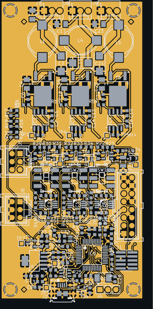
DIOT MONIMOD (OHWR0073 R1) is an open-hardware circuit board from the CERN Open Hardware Repository, designed in KiCad EDA: a 4-layer board of 45.7 × 95.3 mm with 167 components and 105 nets, published under CERN-OHL-W-2.0.
review 94% walked · 23 findings: 2 blocker · 12 major · 9 minor (91 items)
Open in the interactive viewerRead the full review
Design review
Probe recorded 23 findings: 2 blocker · 12 major · 9 minor (91 items) on this design. Each is shown here with its reasoning; the full review links every one to the pins, nets and datasheet pages it rests on.
- CopperShortBetweenNetsblockerOpen
CopperShortBetweenNets: 5 boards×5
5 checked by the review by Claude (Cern session) — 5 different reasons
At short:Net-(D1-Pad1)|Net-(D1-Pad3), short:Net-(D11-Pad1)|Net-(D7-Pad1), short:Net-(D11-Pad3)|Net-(D7-Pad1), short:Net-(D5-Pad1)|Net-(D7-Pad1), short:Net-(D5-Pad1)|Net-(D7-Pad3)
Each finding, with its own headline
short:Net-(D1-Pad1)|Net-(D1-Pad3)Net-(D1-Pad1) and Net-(D1-Pad3) copper touch on F.CU, at (90.36, -113.55): the two nets are shorted in the copper as exported
Net-(D1-Pad1) and Net-(D1-Pad3) copper touch on F.CU, at (90.36, -113.55): the two nets are shorted in the copper as exported. Where: F.CU at (90.36, -113.55) (one net's copper edge lies in the other's copper). The netlist still puts the two nets apart, so every connectivity check passes; the copper the fab builds joins them. The usual cause is a pour filled before the other net's via or pad was placed (or moved), so it runs through it without a clearance: refill the zones, check the CAD tool's DRC is clean, and export again. copper-near at a site shows both nets' copper at distance 0.
short:Net-(D11-Pad1)|Net-(D7-Pad1)Net-(D11-Pad1) and Net-(D7-Pad1) copper touch on F.CU, at (122.95, -104.82): the two nets are shorted in the copper as exported
Net-(D11-Pad1) and Net-(D7-Pad1) copper touch on F.CU, at (122.95, -104.82): the two nets are shorted in the copper as exported. Where: F.CU at (122.95, -104.82) (one net's copper edge lies in the other's copper). The netlist still puts the two nets apart, so every connectivity check passes; the copper the fab builds joins them. The usual cause is a pour filled before the other net's via or pad was placed (or moved), so it runs through it without a clearance: refill the zones, check the CAD tool's DRC is clean, and export again. copper-near at a site shows both nets' copper at distance 0.
short:Net-(D11-Pad3)|Net-(D7-Pad1)Net-(D11-Pad3) and Net-(D7-Pad1) copper touch on F.CU, at (114.24, -114.07): the two nets are shorted in the copper as exported
Net-(D11-Pad3) and Net-(D7-Pad1) copper touch on F.CU, at (114.24, -114.07): the two nets are shorted in the copper as exported. Where: F.CU at (114.24, -114.07) (one net's copper edge lies in the other's copper). The netlist still puts the two nets apart, so every connectivity check passes; the copper the fab builds joins them. The usual cause is a pour filled before the other net's via or pad was placed (or moved), so it runs through it without a clearance: refill the zones, check the CAD tool's DRC is clean, and export again. copper-near at a site shows both nets' copper at distance 0.
short:Net-(D5-Pad1)|Net-(D7-Pad1)Net-(D5-Pad1) and Net-(D7-Pad1) copper touch on F.CU, at (110.36, -104.67): the two nets are shorted in the copper as exported
Net-(D5-Pad1) and Net-(D7-Pad1) copper touch on F.CU, at (110.36, -104.67): the two nets are shorted in the copper as exported. Where: F.CU at (110.36, -104.67) (one net's copper edge lies in the other's copper). The netlist still puts the two nets apart, so every connectivity check passes; the copper the fab builds joins them. The usual cause is a pour filled before the other net's via or pad was placed (or moved), so it runs through it without a clearance: refill the zones, check the CAD tool's DRC is clean, and export again. copper-near at a site shows both nets' copper at distance 0.
short:Net-(D5-Pad1)|Net-(D7-Pad3)Net-(D5-Pad1) and Net-(D7-Pad3) copper touch on F.CU, at (102.14, -113.55): the two nets are shorted in the copper as exported
Net-(D5-Pad1) and Net-(D7-Pad3) copper touch on F.CU, at (102.14, -113.55): the two nets are shorted in the copper as exported. Where: F.CU at (102.14, -113.55) (one net's copper edge lies in the other's copper). The netlist still puts the two nets apart, so every connectivity check passes; the copper the fab builds joins them. The usual cause is a pour filled before the other net's via or pad was placed (or moved), so it runs through it without a clearance: refill the zones, check the CAD tool's DRC is clean, and export again. copper-near at a site shows both nets' copper at distance 0.
- NetCopperSplitblockerOpen
NetCopperSplit: 19 boards×19
19 checked by the review by Claude (Cern session) — 19 different reasons
At split:GND, split:Net-(C14-Pad2), split:Net-(C2-Pad2), split:Net-(C20-Pad2), split:Net-(D1-Pad1), split:Net-(D1-Pad3) and 13 more
Each finding, with its own headline
split:GNDGND's copper is in 4 pieces: T2.2 and 2 other piece(s) are not connected to the rest of the net
GND's copper is in 4 pieces: T2.2 and 2 other piece(s) are not connected to the rest of the net. Piece 1: B1.1, B2.1, B3.1, B4.1, C1.1, C10.1, C11.2, C12.1 and 83 more pin(s), on F.CU, GND, PWR and B.CU, 132 drill(s), 10310.46 mm2 of pour, over (83.56, -175.52) to (128.28, -81.27). Piece 2: T2.2, on F.CU, over (135.72, -108.04) to (138.57, -107.04). Piece 3: T7.2, on F.CU, over (135.72, -124.27) to (138.57, -123.27). Piece 4: T9.2, on F.CU, over (162.23, -108.04) to (165.08, -107.04). The export files every one of these pins under the net, so every connectivity check passes; the copper the fab builds leaves them apart. Usually a pour island that touches only one via of its own net, or a track ending short of its copper: join the piece to the net and export again.
split:Net-(C14-Pad2)Net-(C14-Pad2)'s copper is in 2 pieces: T7.3 is not connected to the rest of the net
Net-(C14-Pad2)'s copper is in 2 pieces: T7.3 is not connected to the rest of the net. Piece 1: C14.2, IC3.6, L4.1 and T3.2, on F.CU, over (101.98, -124.58) to (114.85, -92.21). Piece 2: T7.3, on F.CU, over (140.34, -124.27) to (146.84, -118.72). The export files every one of these pins under the net, so every connectivity check passes; the copper the fab builds leaves them apart. Usually a pour island that touches only one via of its own net, or a track ending short of its copper: join the piece to the net and export again.
split:Net-(C2-Pad2)Net-(C2-Pad2)'s copper is in 2 pieces: T2.3 is not connected to the rest of the net
Net-(C2-Pad2)'s copper is in 2 pieces: T2.3 is not connected to the rest of the net. Piece 1: C2.2, IC1.6, L1.1 and T1.2, on F.CU, over (93.87, -124.58) to (102.92, -97.54). Piece 2: T2.3, on F.CU, over (140.34, -108.04) to (146.84, -102.49). The export files every one of these pins under the net, so every connectivity check passes; the copper the fab builds leaves them apart. Usually a pour island that touches only one via of its own net, or a track ending short of its copper: join the piece to the net and export again.
split:Net-(C20-Pad2)Net-(C20-Pad2)'s copper is in 2 pieces: T9.3 is not connected to the rest of the net
Net-(C20-Pad2)'s copper is in 2 pieces: T9.3 is not connected to the rest of the net. Piece 1: C20.2, IC4.6, L5.1 and T8.2, on F.CU, over (117.74, -126.49) to (124.64, -97.54). Piece 2: T9.3, on F.CU, over (166.85, -108.04) to (173.35, -102.49). The export files every one of these pins under the net, so every connectivity check passes; the copper the fab builds leaves them apart. Usually a pour island that touches only one via of its own net, or a track ending short of its copper: join the piece to the net and export again.
split:Net-(D1-Pad1)Net-(D1-Pad1)'s copper is in 4 pieces: D2.1 and 2 other piece(s) are not connected to the rest of the net
Net-(D1-Pad1)'s copper is in 4 pieces: D2.1 and 2 other piece(s) are not connected to the rest of the net. Piece 1: T1.1, on F.CU, over (90.06, -116.7) to (99.43, -103.4). Piece 2: D2.1, on F.CU, over (135.72, -111.37) to (136.77, -110.72). Piece 3: D2.2, on F.CU, over (135.72, -113.27) to (136.77, -112.62). Piece 4: D1.1, on F.CU, over (148.47, -107.84) to (149.52, -107.19). The export files every one of these pins under the net, so every connectivity check passes; the copper the fab builds leaves them apart. Usually a pour island that touches only one via of its own net, or a track ending short of its copper: join the piece to the net and export again.
split:Net-(D1-Pad3)Net-(D1-Pad3)'s copper is in 3 pieces: D2.3 and 1 other piece(s) are not connected to the rest of the net
Net-(D1-Pad3)'s copper is in 3 pieces: D2.3 and 1 other piece(s) are not connected to the rest of the net. Piece 1: R2.2, on F.CU, over (90.06, -114.55) to (90.96, -113.55). Piece 2: D2.3, on F.CU, over (138.02, -112.32) to (139.07, -111.67). Piece 3: D1.3, on F.CU, over (150.77, -108.79) to (151.82, -108.14). The export files every one of these pins under the net, so every connectivity check passes; the copper the fab builds leaves them apart. Usually a pour island that touches only one via of its own net, or a track ending short of its copper: join the piece to the net and export again.
split:Net-(D10-Pad1)Net-(D10-Pad1)'s copper is in 4 pieces: D10.1 and 2 other piece(s) are not connected to the rest of the net
Net-(D10-Pad1)'s copper is in 4 pieces: D10.1 and 2 other piece(s) are not connected to the rest of the net. Piece 1: T7.1, on F.CU, over (135.72, -119.71) to (138.57, -118.71). Piece 2: D10.1, on F.CU, over (148.47, -124.07) to (149.52, -123.42). Piece 3: D10.2, on F.CU, over (148.47, -125.97) to (149.52, -125.32). Piece 4: D9.1, on F.CU, over (140.67, -127.6) to (141.72, -126.95). The export files every one of these pins under the net, so every connectivity check passes; the copper the fab builds leaves them apart. Usually a pour island that touches only one via of its own net, or a track ending short of its copper: join the piece to the net and export again.
split:Net-(D10-Pad3)Net-(D10-Pad3)'s copper is in 3 pieces: D10.3 and 1 other piece(s) are not connected to the rest of the net
Net-(D10-Pad3)'s copper is in 3 pieces: D10.3 and 1 other piece(s) are not connected to the rest of the net. Piece 1: R53.2, on F.CU, over (154.99, -119.09) to (155.89, -118.09). Piece 2: D10.3, on F.CU, over (150.77, -125.02) to (151.82, -124.37). Piece 3: D9.3, on F.CU, over (142.97, -128.55) to (144.02, -127.9). The export files every one of these pins under the net, so every connectivity check passes; the copper the fab builds leaves them apart. Usually a pour island that touches only one via of its own net, or a track ending short of its copper: join the piece to the net and export again.
split:Net-(D11-Pad1)Net-(D11-Pad1)'s copper is in 4 pieces: D11.1 and 2 other piece(s) are not connected to the rest of the net
Net-(D11-Pad1)'s copper is in 4 pieces: D11.1 and 2 other piece(s) are not connected to the rest of the net. Piece 1: T8.1, on F.CU, over (122.3, -106.25) to (123.3, -103.4). Piece 2: D11.1, on F.CU, over (174.98, -107.84) to (176.03, -107.19). Piece 3: D12.1, on F.CU, over (167.18, -111.37) to (168.23, -110.72). Piece 4: D12.2, on F.CU, over (167.18, -113.27) to (168.23, -112.62). The export files every one of these pins under the net, so every connectivity check passes; the copper the fab builds leaves them apart. Usually a pour island that touches only one via of its own net, or a track ending short of its copper: join the piece to the net and export again.
split:Net-(D11-Pad3)Net-(D11-Pad3)'s copper is in 3 pieces: D11.3 and 1 other piece(s) are not connected to the rest of the net
Net-(D11-Pad3)'s copper is in 3 pieces: D11.3 and 1 other piece(s) are not connected to the rest of the net. Piece 1: R54.2, on F.CU, over (113.94, -114.55) to (114.84, -113.55). Piece 2: D11.3, on F.CU, over (177.28, -108.79) to (178.33, -108.14). Piece 3: D12.3, on F.CU, over (169.48, -112.32) to (170.53, -111.67). The export files every one of these pins under the net, so every connectivity check passes; the copper the fab builds leaves them apart. Usually a pour island that touches only one via of its own net, or a track ending short of its copper: join the piece to the net and export again.
split:Net-(D13-Pad1)Net-(D13-Pad1)'s copper is in 4 pieces: D14.2 and 2 other piece(s) are not connected to the rest of the net
Net-(D13-Pad1)'s copper is in 4 pieces: D14.2 and 2 other piece(s) are not connected to the rest of the net. Piece 1: D14.1, on F.CU, over (162.23, -111.37) to (163.28, -110.72). Piece 2: D14.2, on F.CU, over (162.23, -113.27) to (163.28, -112.62). Piece 3: D13.1, on F.CU, over (174.98, -103.02) to (176.03, -102.37). Piece 4: T9.1, on F.CU, over (162.23, -103.48) to (165.08, -102.48). The export files every one of these pins under the net, so every connectivity check passes; the copper the fab builds leaves them apart. Usually a pour island that touches only one via of its own net, or a track ending short of its copper: join the piece to the net and export again.
split:Net-(D13-Pad3)Net-(D13-Pad3)'s copper is in 3 pieces: D14.3 and 1 other piece(s) are not connected to the rest of the net
Net-(D13-Pad3)'s copper is in 3 pieces: D14.3 and 1 other piece(s) are not connected to the rest of the net. Piece 1: R55.2, on F.CU, over (181.5, -102.86) to (182.4, -101.86). Piece 2: D14.3, on F.CU, over (164.53, -112.32) to (165.58, -111.67). Piece 3: D13.3, on F.CU, over (177.28, -103.97) to (178.33, -103.32). The export files every one of these pins under the net, so every connectivity check passes; the copper the fab builds leaves them apart. Usually a pour island that touches only one via of its own net, or a track ending short of its copper: join the piece to the net and export again.
split:Net-(D5-Pad1)Net-(D5-Pad1)'s copper is in 4 pieces: D5.1 and 2 other piece(s) are not connected to the rest of the net
Net-(D5-Pad1)'s copper is in 4 pieces: D5.1 and 2 other piece(s) are not connected to the rest of the net. Piece 1: T2.1, on F.CU, over (135.72, -103.48) to (138.57, -102.48). Piece 2: D5.1, on F.CU, over (148.47, -103.02) to (149.52, -102.37). Piece 3: D6.1, on F.CU, over (140.67, -111.37) to (141.72, -110.72). Piece 4: D6.2, on F.CU, over (140.67, -113.27) to (141.72, -112.62). The export files every one of these pins under the net, so every connectivity check passes; the copper the fab builds leaves them apart. Usually a pour island that touches only one via of its own net, or a track ending short of its copper: join the piece to the net and export again.
split:Net-(D5-Pad3)Net-(D5-Pad3)'s copper is in 3 pieces: D5.3 and 1 other piece(s) are not connected to the rest of the net
Net-(D5-Pad3)'s copper is in 3 pieces: D5.3 and 1 other piece(s) are not connected to the rest of the net. Piece 1: R13.2, on F.CU, over (154.99, -102.86) to (155.89, -101.86). Piece 2: D5.3, on F.CU, over (150.77, -103.97) to (151.82, -103.32). Piece 3: D6.3, on F.CU, over (142.97, -112.32) to (144.02, -111.67). The export files every one of these pins under the net, so every connectivity check passes; the copper the fab builds leaves them apart. Usually a pour island that touches only one via of its own net, or a track ending short of its copper: join the piece to the net and export again.
split:Net-(D7-Pad1)Net-(D7-Pad1)'s copper is in 4 pieces: D8.1 and 2 other piece(s) are not connected to the rest of the net
Net-(D7-Pad1)'s copper is in 4 pieces: D8.1 and 2 other piece(s) are not connected to the rest of the net. Piece 1: T3.1, on F.CU, over (110.36, -106.25) to (111.36, -103.4). Piece 2: D8.1, on F.CU, over (148.47, -119.25) to (149.52, -118.6). Piece 3: D8.2, on F.CU, over (148.47, -121.15) to (149.52, -120.5). Piece 4: D7.1, on F.CU, over (135.72, -127.6) to (136.77, -126.95). The export files every one of these pins under the net, so every connectivity check passes; the copper the fab builds leaves them apart. Usually a pour island that touches only one via of its own net, or a track ending short of its copper: join the piece to the net and export again.
split:Net-(D7-Pad3)Net-(D7-Pad3)'s copper is in 3 pieces: D8.3 and 1 other piece(s) are not connected to the rest of the net
Net-(D7-Pad3)'s copper is in 3 pieces: D8.3 and 1 other piece(s) are not connected to the rest of the net. Piece 1: R15.2, on F.CU, over (102, -114.55) to (102.9, -113.55). Piece 2: D8.3, on F.CU, over (150.77, -120.2) to (151.82, -119.55). Piece 3: D7.3, on F.CU, over (138.02, -128.55) to (139.07, -127.9). The export files every one of these pins under the net, so every connectivity check passes; the copper the fab builds leaves them apart. Usually a pour island that touches only one via of its own net, or a track ending short of its copper: join the piece to the net and export again.
split:Net-(IC1-Pad4)Net-(IC1-Pad4)'s copper is in 2 pieces: R13.1 is not connected to the rest of the net
Net-(IC1-Pad4)'s copper is in 2 pieces: R13.1 is not connected to the rest of the net. Piece 1: IC1.4, on F.CU, over (97.49, -122.35) to (98.09, -120.8). Piece 2: R13.1, on F.CU, over (153.39, -102.86) to (154.29, -101.86). The export files every one of these pins under the net, so every connectivity check passes; the copper the fab builds leaves them apart. Usually a pour island that touches only one via of its own net, or a track ending short of its copper: join the piece to the net and export again.
split:Net-(IC3-Pad4)Net-(IC3-Pad4)'s copper is in 2 pieces: R53.1 is not connected to the rest of the net
Net-(IC3-Pad4)'s copper is in 2 pieces: R53.1 is not connected to the rest of the net. Piece 1: IC3.4, on F.CU, over (109.43, -122.35) to (110.03, -120.8). Piece 2: R53.1, on F.CU, over (153.39, -119.09) to (154.29, -118.09). The export files every one of these pins under the net, so every connectivity check passes; the copper the fab builds leaves them apart. Usually a pour island that touches only one via of its own net, or a track ending short of its copper: join the piece to the net and export again.
split:Net-(IC4-Pad4)Net-(IC4-Pad4)'s copper is in 2 pieces: R55.1 is not connected to the rest of the net
Net-(IC4-Pad4)'s copper is in 2 pieces: R55.1 is not connected to the rest of the net. Piece 1: IC4.4, on F.CU, over (121.37, -122.35) to (121.97, -120.8). Piece 2: R55.1, on F.CU, over (179.9, -102.86) to (180.8, -101.86). The export files every one of these pins under the net, so every connectivity check passes; the copper the fab builds leaves them apart. Usually a pour island that touches only one via of its own net, or a track ending short of its copper: join the piece to the net and export again.
Vref25 reference IC7 (TL431) is biased with 0.40 mA but its own sensor current sources draw about 1 mA per channel from it
The 2.5 V reference Vref25 cannot stay in regulation: R28 (2 k from P3V3_AUX) feeds IC7 (TL431B) only about 0.40 mA, below the TL431's 1 mA minimum operating current, while each temperature channel's current source pulls up to about 1 mA from the same node through R38/R44/R50. Vref25 is also the MCU ADC reference (VREFA), so every non-ratiometric ADC reading moves with it.
The bias is below the TL431's operating minimum even with no load
Quantity Value Source Supply to Vref25 P3V3_AUX (3.3 V via L2 from P3V3) netlist R28.2 Bias resistor R28 2 k, 1 % BOM Available current at 2.495 V (3.3 - 2.495) / 2 k = 0.40 mA computed TL431 recommended cathode current 1 mA min, 100 mA max Nexperia TL431 Rev. 8, Table 8, p6 TL431B minimum cathode current I_K(min) 0.4 typ, 0.6 max mA Table 10, p8 The loads on Vref25 are larger than the bias
Each temperature channel is an improved Howland current source (IC10/IC11/IC12 OPA2192 with R35-R38, R41-R44, R47-R50, all 2k49). It sets I = Vref25 / 2k49 = 1.0 mA in the sensor, and the share drawn from Vref25 through R38 (R44, R50) is (Vref25 - V_sensor) / 2k49. With an RTD-class sensor (the x17 amplifier, R40 16 k / R39 1 k, implies about 0.1 V across the sensor) that is about 0.96 mA per channel in current-source mode (DPDT SW1-SW3).
Channels in current-source mode Vref25 node (TL431 off, solved R28 vs loads) 0 2.495 V, but IC7 at 0.40 mA, below its 1 mA minimum 1 about 1.9 V 3 about 1.0 V ``
mermaid flowchart LR P3V3_AUX -->|R28 2k, 0.40 mA| VREF[Vref25] VREF --> IC7[IC7 TL431 shunt] VREF -->|R38 2k49, ~1 mA| CS1[Ch1 Howland] VREF -->|R44 2k49, ~1 mA| CS2[Ch2 Howland] VREF -->|R50 2k49, ~1 mA| CS3[Ch3 Howland] VREF --> MCU[IC6 PA03 VREFA]``Why it matters
The RTD readings stay roughly ratiometric (sensor current and ADC reference both scale with Vref25), which may be why it works on the bench. Anything else the ADC converts against VREFA (the V_adc and VI_adc channels) reads high by 2.495 V / Vref25, up to about 2.4x, and changes as channels are switched. If firmware uses the internal reference instead, the TL431 is still out of its operating range. A smaller R28 (for example about 270 R for 3 mA of loads plus 1 mA bias) or a buffered reference would fix it.
18 BOM-fitted parts, including all three low-side fan MOSFETs and their gate networks, are placed outside the board outline in the layout data
In the ODB++ of OHWR0073 R1 DIOT MONIMOD, 18 components that the BOM lists as fitted sit outside the board outline (x 83-129 mm, y -176 to -81 mm): the low-side MOSFETs T2, T7, T9 of the three fan buck stages, the gate zeners D1, D5, D7, D9, D11, D13, the gate-discharge diodes D2, D6, D8, D10, D12, D14 and the low-side gate resistors R13, R53, R55. Built from this data, none of them is on the board: the synchronous bucks (schematic sheet 8, 'Fan drivers') lose their low-side switch and both gate networks, including D1/D2 in the gate path of the on-board high-side switch T1.
Ref Part Placement (mm) Source T2, T7, T9 IPD5N25S3-430 (141.3, -105.3), (141.3, -121.5), (167.8, -105.3) ODB++ placement D1, D5, D7, D9, D11, D13 BZX84C5V1 x 137-177, y -104 to -128 ODB++ placement D2, D6, D8, D10, D12, D14 BAT54C x 137-169, y -112 to -125 ODB++ placement R13, R53, R55 10 R 0603 x 155-181, y -102 to -119 ODB++ placement Board outline x 83.06-128.78, y -176.02 to -80.77 ODB++ profile ``
mermaid flowchart LR IC1[IC1 L6498 HVG] --> R2 --> GN1[D1 + D2: off board] --> T1[T1 high side, on board] IC1b[IC1 L6498 LVG] --> R13[R13: off board] --> GN2[D5 + D6: off board] --> T2[T2 low side: off board] T1 --> SW[switch node] --> L1 --> FAN[Fan_out1] T2 --> SW``Why it matters
Either the layout was released with these footprints never placed on the PCB, or they are intentionally unpopulated and the BOM says otherwise. In the first case an assembled board has no low-side switch and no drive path to T1's gate (the netlist joins T1 gate only through D1/D2); in the second, the BOM and the design data disagree and the fan stages would have to run asynchronously without a freewheel diode. Either way the release data does not describe a buildable fan driver. The other MoniMod variants (FANTRAY, RATOPUS) place all their parts inside the outline.
BAT54C went end-of-life (Obsolete)
Vendor (DigiKey) lifecycle for BAT54C (onsemi's listing) changed from "Active" to "Obsolete" since this board was reviewed. Placed as D10, D12, D14, D2, D6, D8. A sourcing/longevity risk; consider a replacement before production.
BZX84C5V1 went end-of-life (Obsolete)
Vendor (DigiKey) lifecycle for BZX84C5V1 (onsemi's listing) changed from "Active" to "Obsolete" since this board was reviewed. Placed as D1, D11, D13, D5, D7, D9. A sourcing/longevity risk; consider a replacement before production.
- concernCON-001majorOpen
[eol:BAT54C:Obsolete] BAT54C lifecycle changed from "Active" to "Obsolete" since this board was reviewed: OHWR0073 R1 DIOT MONIMOD. A sourcing and longevity risk. Should this be replaced before the next build?
- concernCON-002majorOpen
[eol:BZX84C5V1:Obsolete] BZX84C5V1 lifecycle changed from "Active" to "Obsolete" since this board was reviewed: OHWR0073 R1 DIOT MONIMOD. A sourcing and longevity risk. Should this be replaced before the next build?
- DecapViaFanoutmajorOpen
DecapViaFanout: 5 components×5
Checked by the review, stands · Claude walker W1 (Cern session) — Checked: fan-out lengths read from the copper stand; the 0.5 nH limit is Probe's starting value, not a datasheet requirement for these parts, and no PDN target is stated. Not refutable with a citation; left for the owner.
At C12, C18, C24, C31, C6
Each finding, with its own headline
C12C12 on 'P3V3': its rail pad reaches its via over 3.14 mm of track, adding about 1.08 nH to its loop, past Probe's 0.5 nH starting value; put the vias at the pads
C12 on 'P3V3': its rail pad reaches its via over 3.14 mm of track, adding about 1.08 nH to its loop, past Probe's 0.5 nH starting value; put the vias at the pads. C12.2 (rail) runs 3.14 mm along its copper to its nearest via, 2.14 mm past the 1 mm beside the pad: 1.08 nH; C12.1 (ground) not measured: the pad sits in a pour of its net on its own layer, which has no track length to measure. Each run past the pad as one conductor of a pair 1.60 mm apart (the pad pitch), 0.2 l ln(D/R) nH with R 0.127 mm (the track's width is not read): 1.08 nH in all. Put the vias at the pads (or in them), one per pad at least, the rail's and the ground's close together; the capacitor's own inductance as mounted is 1.19 nH (pad 0.10 nH + no via of the first net within 1 mm of its pad: the study's 0.6 nH per mm of 0.96 mm depth, ASSUMED). 0.5 nH is Probe's starting value, about the whole mounted inductance of a well-mounted 0402.
C18C18 on 'P12V': its rail pad reaches its via over 6.00 mm of track, adding about 2.53 nH to its loop, past Probe's 0.5 nH starting value; put the vias at the pads
C18 on 'P12V': its rail pad reaches its via over 6.00 mm of track, adding about 2.53 nH to its loop, past Probe's 0.5 nH starting value; put the vias at the pads. C18.2 (rail) runs at least 6.00 mm along its copper to its nearest via, 5.00 mm past the 1 mm beside the pad: 2.53 nH; C18.1 (ground) not measured: the pad sits in a pour of its net on its own layer, which has no track length to measure. Each run past the pad as one conductor of a pair 1.60 mm apart (the pad pitch), 0.2 l ln(D/R) nH with R 0.127 mm (the track's width is not read): 2.53 nH in all. Put the vias at the pads (or in them), one per pad at least, the rail's and the ground's close together; the capacitor's own inductance as mounted is 1.19 nH (pad 0.10 nH + no via of the first net within 1 mm of its pad: the study's 0.6 nH per mm of 0.96 mm depth, ASSUMED). 0.5 nH is Probe's starting value, about the whole mounted inductance of a well-mounted 0402.
C24C24 on 'P12V': its rail pad reaches its via over 6.00 mm of track, adding about 2.53 nH to its loop, past Probe's 0.5 nH starting value; put the vias at the pads
C24 on 'P12V': its rail pad reaches its via over 6.00 mm of track, adding about 2.53 nH to its loop, past Probe's 0.5 nH starting value; put the vias at the pads. C24.2 (rail) runs at least 6.00 mm along its copper to its nearest via, 5.00 mm past the 1 mm beside the pad: 2.53 nH; C24.1 (ground) not measured: the pad sits in a pour of its net on its own layer, which has no track length to measure. Each run past the pad as one conductor of a pair 1.60 mm apart (the pad pitch), 0.2 l ln(D/R) nH with R 0.127 mm (the track's width is not read): 2.53 nH in all. Put the vias at the pads (or in them), one per pad at least, the rail's and the ground's close together; the capacitor's own inductance as mounted is 1.19 nH (pad 0.10 nH + no via of the first net within 1 mm of its pad: the study's 0.6 nH per mm of 0.96 mm depth, ASSUMED). 0.5 nH is Probe's starting value, about the whole mounted inductance of a well-mounted 0402.
C31C31 on 'P3V3': its rail pad reaches its via over 2.36 mm of track, adding about 0.69 nH to its loop, past Probe's 0.5 nH starting value; put the vias at the pads
C31 on 'P3V3': its rail pad reaches its via over 2.36 mm of track, adding about 0.69 nH to its loop, past Probe's 0.5 nH starting value; put the vias at the pads. C31.2 (rail) runs 2.36 mm along its copper to its nearest via, 1.36 mm past the 1 mm beside the pad: 0.69 nH; C31.1 (ground) not measured: the pad sits in a pour of its net on its own layer, which has no track length to measure. Each run past the pad as one conductor of a pair 1.60 mm apart (the pad pitch), 0.2 l ln(D/R) nH with R 0.127 mm (the track's width is not read): 0.69 nH in all. Put the vias at the pads (or in them), one per pad at least, the rail's and the ground's close together; the capacitor's own inductance as mounted is 1.19 nH (pad 0.10 nH + no via of the first net within 1 mm of its pad: the study's 0.6 nH per mm of 0.96 mm depth, ASSUMED). 0.5 nH is Probe's starting value, about the whole mounted inductance of a well-mounted 0402.
C6C6 on 'P12V': its rail pad reaches its via over 6.00 mm of track, adding about 2.53 nH to its loop, past Probe's 0.5 nH starting value; put the vias at the pads
C6 on 'P12V': its rail pad reaches its via over 6.00 mm of track, adding about 2.53 nH to its loop, past Probe's 0.5 nH starting value; put the vias at the pads. C6.2 (rail) runs at least 6.00 mm along its copper to its nearest via, 5.00 mm past the 1 mm beside the pad: 2.53 nH; C6.1 (ground) not measured: the pad sits in a pour of its net on its own layer, which has no track length to measure. Each run past the pad as one conductor of a pair 1.60 mm apart (the pad pitch), 0.2 l ln(D/R) nH with R 0.127 mm (the track's width is not read): 2.53 nH in all. Put the vias at the pads (or in them), one per pad at least, the rail's and the ground's close together; the capacitor's own inductance as mounted is 1.19 nH (pad 0.10 nH + no via of the first net within 1 mm of its pad: the study's 0.6 nH per mm of 0.96 mm depth, ASSUMED). 0.5 nH is Probe's starting value, about the whole mounted inductance of a well-mounted 0402.
- EsdProtectorPlacementmajorOpen
EsdProtectorPlacement: 4 components×4
Checked by the review, stands · Claude walker W1 (Cern session) — Checked: D3 is reached through two vias and sits 20-29 mm from J1/J3; read from the copper and it stands. Raised as OBS-496.
At D3
Each finding, with its own headline
D3D3.1 on '/connectors/m_io2': 2 via(s) between J1.2 and D3.1
D3 (PESD3V3S5UD) protects '/connectors/m_io2' at J1.2. Along the copper: 39.66 mm of track from the contact, 2 via(s) before it, on a 1.34 mm branch off the line; the line runs 38.33 mm on to R5.2; D3 sits 18.98 mm farther from the contact than the nearest place outside J1.
2 via(s) between J1.2 and D3.1: the strike reaches an inner layer before it is clamped. D3.1 hangs 1.34 mm off the line (limit 1 mm, default: no datasheet figure on file): the line carries the strike past it while the clamp is reached through the branch. D3 joins the line 38.32 mm from J1.2 on a 38.33 mm run to R5.2: nearer the far end than the contact, so the surge travels most of the line before it is clamped.
Measured on the copper the ODB states: tracks, the pads they land on, and the netlist's vias. Not a straight line between centroids.
D3D3.3 on '/connectors/m_io1': 2 via(s) between J1.4 and D3.3
D3 (PESD3V3S5UD) protects '/connectors/m_io1' at J1.4. Along the copper: 38.57 mm of track from the contact, 2 via(s) before it, the line runs through its pad (flow-through); the line runs 40.3 mm on to R4.2; D3 sits 17.78 mm farther from the contact than the nearest place outside J1.
2 via(s) between J1.4 and D3.3: the strike reaches an inner layer before it is clamped. D3 joins the line 38.57 mm from J1.4 on a 40.3 mm run to R4.2: nearer the far end than the contact, so the surge travels most of the line before it is clamped.
Measured on the copper the ODB states: tracks, the pads they land on, and the netlist's vias. Not a straight line between centroids.
D3D3.4 on '/connectors/m_sda': 2 via(s) between J3.9 and D3.4
D3 (PESD3V3S5UD) protects '/connectors/m_sda' at J3.9. Along the copper: 47.63 mm of track from the contact, 2 via(s) before it, on a 1.77 mm branch off the line; the line runs 45.91 mm on to R25.1; D3 sits 22.96 mm farther from the contact than the nearest place outside J3.
2 via(s) between J3.9 and D3.4: the strike reaches an inner layer before it is clamped. D3.4 hangs 1.77 mm off the line (limit 1 mm, default: no datasheet figure on file): the line carries the strike past it while the clamp is reached through the branch. D3 joins the line 45.86 mm from J3.9 on a 45.91 mm run to R25.1: nearer the far end than the contact, so the surge travels most of the line before it is clamped.
Measured on the copper the ODB states: tracks, the pads they land on, and the netlist's vias. Not a straight line between centroids.
D3D3.5 on '/connectors/m_scl': 2 via(s) between J3.5 and D3.5
D3 (PESD3V3S5UD) protects '/connectors/m_scl' at J3.5. Along the copper: 39.03 mm of track from the contact, 2 via(s) before it, on a 5.73 mm branch off the line; the line runs 33.29 mm on to R26.1; D3 sits 19.19 mm farther from the contact than the nearest place outside J3.
2 via(s) between J3.5 and D3.5: the strike reaches an inner layer before it is clamped. D3.5 hangs 5.73 mm off the line (limit 1 mm, default: no datasheet figure on file): the line carries the strike past it while the clamp is reached through the branch. D3 joins the line 33.3 mm from J3.5 on a 33.29 mm run to R26.1: nearer the far end than the contact, so the surge travels most of the line before it is clamped.
Measured on the copper the ODB states: tracks, the pads they land on, and the netlist's vias. Not a straight line between centroids.
- PartLifecyclemajorOpen
PartLifecycle: 2 part numbers×2
2 Obsolete · on 12 placements
At D1, D10
Each finding, with its own headline
D1BZX84C5V1 on 6 placements (D1, D11, D13, D5, D7, D9): the distributor catalogue reports "Obsolete" for onsemi's BZX84C5V1
BZX84C5V1 on 6 placements (D1, D11, D13, D5, D7, D9): the distributor catalogue reports "Obsolete" for onsemi's BZX84C5V1 — a sourcing/longevity risk to confirm against the MANUFACTURER before acting. This board's BOM names no manufacturer for it, so whether that is the fitted maker's product was not checked. A distributor delisting is not the same claim as the part being unavailable; check the vendor's own lifecycle/product-change notice for the status and any named successor. Re-read the source: GET /api/odb/parts/BZX84C5V1/providers (which provider said it, the maker and part number it matched, its own words, and when we asked). THE LAST BUY DATE HAS PASSED (2017-11-19, 3,283 day(s) ago), so this is a substitution rather than a buy. The distributor reports NONE left. No approved alternate is recorded for this position.
D10BAT54C on 6 placements (D10, D12, D14, D2, D6, D8): the distributor catalogue reports "Obsolete" for onsemi's BAT54C
BAT54C on 6 placements (D10, D12, D14, D2, D6, D8): the distributor catalogue reports "Obsolete" for onsemi's BAT54C — a sourcing/longevity risk to confirm against the MANUFACTURER before acting. This board's BOM names no manufacturer for it, so whether that is the fitted maker's product was not checked. A distributor delisting is not the same claim as the part being unavailable; check the vendor's own lifecycle/product-change notice for the status and any named successor. Re-read the source: GET /api/odb/parts/BAT54C/providers (which provider said it, the maker and part number it matched, its own words, and when we asked). THE LAST BUY DATE HAS PASSED (2018-09-30, 2,968 day(s) ago), so this is a substitution rather than a buy. The distributor reports 54,983 left. No approved alternate is recorded for this position.
- ReferencePlaneDiscontinuitymajorOpen
ReferencePlaneDiscontinuity: 17 boards×17
Checked by the review, stands · Claude walker W1 (Cern session) — Checked: splits, voids and reference changes read from the copper stand as reported; they sit on slow monitoring, I2C, fan-control and reset nets of a 48 MHz microcontroller board, and no datasheet or app note on file sets a limit for them. Not refutable with a citation; left for the owner.
At along@PWR:P12V|P3V3, refchange:GND|P12V, split@PWR:+5VA|GND, split@PWR:+5VA|P12V, split@PWR:+5VA|P3V3, split@PWR:GND|P12V and 11 more
Each finding, with its own headline
along@PWR:P12V|P3V3'/connectors/Fan_tacho3' runs ALONG the split between the P12V and P3V3 planes on PWR at 1 place, the longest 19.75 mm; the impedance rises from 83 ohm to 99 ohm there at worst, 8.7 % of each edge reflected (fastest: /connectors/Fan_tacho3 at 100 ps 10-90 %, ASSUMED)
On PWR the P12V and P3V3 planes part, and '/connectors/Fan_tacho3' runs down the slot between them at 1 place(s), rather than across it. This is not a crossing: the return still follows the track, in the plane on its other side and in the slot's edges, so it does not detour. What changes is the track's own impedance. With the plane gone from under it on this side for that length, its field reaches further, to the slot's edges and to the next plane beyond, so its capacitance falls and its impedance rises; every edge travelling down it is partly reflected where it enters the stretch and again where it leaves, by (Z2 - Z1)/(Z2 + Z1). The longer the stretch against the edge's rise, the more of the edge sees the full step. A crossing is generally the worse fault; a mismatch is not free. Over solid plane each track is 83 ohm; along the slot 99 ohm, reflecting up to 8.7 % of each edge (a method-of-moments field solve of the cross-section, one dielectric; were the slot's edges to carry none of the return, up to 103 ohm). No place stays within 10 %, the tolerance controlled impedance is commonly built to (the stackup states none), so the finding is a warning. One decision covers the split line's slot: whether these tracks may run down it, or should be moved over solid plane.
- '/connectors/Fan_tacho3' on B.CU at (119.97, -141.31), 21.04 mm, running ALONG the split for 19.75 mm, not across it, 83 ohm over solid plane, 99 ohm along it: 8.7 % of each edge reflected; other side: none: the signal layer is outermost
Every site is a row of this finding's evidence, keyed by net, layers and position. GET /api/odb/boards/74/reference-planes?group=along%40PWR%3AP12V%7CP3V3 serves each with its own layer_image region; all of them lie in x 117.74..120.97, y -153.83..-130.7 mm (board frame, Y up).
Read from the copper as drawn on the reference layer, along each track's centreline at exact breakpoints. The reference is the copper beside the track, never the layer's type or name. Whether it matters depends on each signal's edge rate, which nothing on file states for these nets: a slow static line crosses a split harmlessly, a fast edge does not.
refchange:GND|P12V7 nets change reference between GND and P12V at 8 vias, none with a reference that continues across (fastest: /Fan_ctrl1 at 100 ps 10-90 %, ASSUMED)
At 8 via(s), on 7 net(s), the signal leaves a layer referenced by one of GND and P12V for a layer referenced by the other, and no plane references both layers. Different nets: no via can carry the return across; only decoupling between the two planes near the via can. The capacitor carrying the return across was measured at each via, at the knee of the crossing net's edge against 50 ohm assumed: 8 with none. 8 of them at an ASSUMED edge (no edge on file for the net): state one (net_timing_state) and it is re-read. One decision covers the pair: whether GND and P12V are decoupled to each other near these vias. A via whose layers have more references than these two is a site of each pair it joins. None is partial: at every one, no reference continues across the via.
- '/Fan_ctrl1' at (94.23, -124.71), F.CU -> B.CU: GND on GND to P12V on PWR; pure, no reference continues across; stitching none, 49.3 mm of track past the via on B.CU: At the 5 GHz knee of a 100 ps edge (100 ps 10-90 %, assumed: no edge is on file for the net) no capacitor carries the return; only the planes do. GND and P12V are not a thin pair (at most 0.2 mm), so their own capacitance does not carry the return. To serve it, change layers across the same plane, or move the signal to a layer referenced to ground. None.
- '/Fan_ctrl2' at (106.3, -124.97), F.CU -> B.CU: GND on GND to P12V on PWR; pure, no reference continues across; stitching none, 41.4 mm of track past the via on B.CU: At the 5 GHz knee of a 100 ps edge (100 ps 10-90 %, assumed: no edge is on file for the net) no capacitor carries the return; only the planes do. GND and P12V are not a thin pair (at most 0.2 mm), so their own capacitance does not carry the return. To serve it, change layers across the same plane, or move the signal to a layer referenced to ground. None.
- '/Fan_ctrl3' at (116.08, -124.97), F.CU -> B.CU: GND on GND to P12V on PWR; pure, no reference continues across; stitching none, 35.9 mm of track past the via on B.CU: At the 5 GHz knee of a 100 ps edge (100 ps 10-90 %, assumed: no edge is on file for the net) no capacitor carries the return; only the planes do. GND and P12V are not a thin pair (at most 0.2 mm), so their own capacitance does not carry the return. To serve it, change layers across the same plane, or move the signal to a layer referenced to ground. None.
- '/VI_adc1' at (104.58, -133.71), F.CU -> B.CU: GND on GND to P12V on PWR; pure, no reference continues across; stitching none, 33.9 mm of track past the via on B.CU: At the 5 GHz knee of a 100 ps edge (100 ps 10-90 %, assumed: no edge is on file for the net) no capacitor carries the return; only the planes do. GND and P12V are not a thin pair (at most 0.2 mm), so their own capacitance does not carry the return. To serve it, change layers across the same plane, or move the signal to a layer referenced to ground. None.
- '/VI_adc2' at (104.18, -133.01), F.CU -> B.CU: GND on GND to P12V on PWR; pure, no reference continues across; stitching none, 30.0 mm of track past the via on B.CU: At the 5 GHz knee of a 100 ps edge (100 ps 10-90 %, assumed: no edge is on file for the net) no capacitor carries the return; only the planes do. GND and P12V are not a thin pair (at most 0.2 mm), so their own capacitance does not carry the return. To serve it, change layers across the same plane, or move the signal to a layer referenced to ground. None.
- '/V_in1' at (94.74, -132.51), F.CU -> B.CU: GND on GND to P12V on PWR; pure, no reference continues across; stitching none, 25.8 mm of track past the via on B.CU: At the 5 GHz knee of a 100 ps edge (100 ps 10-90 %, assumed: no edge is on file for the net) no capacitor carries the return; only the planes do. GND and P12V are not a thin pair (at most 0.2 mm), so their own capacitance does not carry the return. To serve it, change layers across the same plane, or move the signal to a layer referenced to ground. None.
- '/V_in1' at (97.03, -125.6), F.CU -> B.CU: GND on GND to P12V on PWR; pure, no reference continues across; stitching none, 25.8 mm of track past the via on B.CU: At the 5 GHz knee of a 100 ps edge (100 ps 10-90 %, assumed: no edge is on file for the net) no capacitor carries the return; only the planes do. GND and P12V are not a thin pair (at most 0.2 mm), so their own capacitance does not carry the return. To serve it, change layers across the same plane, or move the signal to a layer referenced to ground. None.
- '/VI_adc3' at (100.96, -132.97), F.CU -> B.CU: GND on GND to P12V on PWR; pure, no reference continues across; stitching none, 19.1 mm of track past the via on B.CU: At the 5 GHz knee of a 100 ps edge (100 ps 10-90 %, assumed: no edge is on file for the net) no capacitor carries the return; only the planes do. GND and P12V are not a thin pair (at most 0.2 mm), so their own capacitance does not carry the return. To serve it, change layers across the same plane, or move the signal to a layer referenced to ground. None.
Every site is a row of this finding's evidence, keyed by net, layers and position. GET /api/odb/boards/74/reference-planes?group=refchange%3AGND%7CP12V serves each with its own layer_image region; all of them lie in x 92.23..118.08, y -135.71..-122.71 mm (board frame, Y up).
The reference on each layer is the first plane the track meets leaving the via, anti-pads and the net's own copper skipped. Whether it matters depends on each signal's edge rate, which nothing on file states for these nets: a slow static line crosses a split harmlessly, a fast edge does not.
split@PWR:+5VA|GND'/Voltage_dividers/V_adc1' crosses the split between the +5VA and GND planes on PWR at 1 place, with no plane on the track's other side (fastest: /Voltage_dividers/V_adc1 at 100 ps 10-90 %, ASSUMED)
On PWR the +5VA and GND planes part, and '/Voltage_dividers/V_adc1' crosses from one to the other at 1 place(s). The return current cannot follow a track across; it detours to wherever the two planes are joined (a stitching capacitor, or the source), and the loop it opens radiates and couples. One decision covers the boundary: whether it is stitched near these crossings, or the nets crossing it are slow enough not to care. Tracks that run ALONG this split, down the slot rather than across it, are a finding of their own: theirs is an impedance step, not a detour. At 0 of the 1 crossing(s) the track's other neighbour carries a plane, which the return can use there; 1 are on an outer layer, with no other neighbour. No crossing has a plane on the track's other side, so the whole return meets the break.
- '/Voltage_dividers/V_adc1' on B.CU at (93.09, -151.19), 1.07 mm; other side: none: the signal layer is outermost
Every site is a row of this finding's evidence, keyed by net, layers and position. GET /api/odb/boards/74/reference-planes?group=split%40PWR%3A%2B5VA%7CGND serves each with its own layer_image region; all of them lie in x 91.71..94.47, y -152.57..-149.81 mm (board frame, Y up).
Read from the copper as drawn on the reference layer, along each track's centreline at exact breakpoints. The reference is the copper beside the track, never the layer's type or name. Whether it matters depends on each signal's edge rate, which nothing on file states for these nets: a slow static line crosses a split harmlessly, a fast edge does not.
split@PWR:+5VA|P12V8 nets cross the split between the +5VA and P12V planes on PWR at 8 places, with no plane on the track's other side (fastest: /Fan_ctrl1 at 100 ps 10-90 %, ASSUMED)
On PWR the +5VA and P12V planes part, and 8 nets cross from one to the other at 8 place(s). The return current cannot follow a track across; it detours to wherever the two planes are joined (a stitching capacitor, or the source), and the loop it opens radiates and couples. One decision covers the boundary: whether it is stitched near these crossings, or the nets crossing it are slow enough not to care. Tracks that run ALONG this split, down the slot rather than across it, are a finding of their own: theirs is an impedance step, not a detour. At 0 of the 8 crossing(s) the track's other neighbour carries a plane, which the return can use there; 8 are on an outer layer, with no other neighbour. No crossing has a plane on the track's other side, so the whole return meets the break.
- '/Fan_ctrl1' on B.CU at (101.22, -136.21), 0.64 mm; other side: none: the signal layer is outermost
- '/Fan_ctrl2' on B.CU at (113.03, -136.17), 0.73 mm; other side: none: the signal layer is outermost
- '/Fan_ctrl3' on B.CU at (114.81, -136.21), 0.64 mm; other side: none: the signal layer is outermost
- '/VI_adc1' on B.CU at (103.76, -136.21), 0.64 mm; other side: none: the signal layer is outermost
- '/VI_adc2' on B.CU at (103.36, -136.21), 0.64 mm; other side: none: the signal layer is outermost
- '/VI_adc3' on B.CU at (100.82, -136.21), 0.64 mm; other side: none: the signal layer is outermost
- '/connectors/Fan_tacho1' on B.CU at (101.82, -136.21), 0.64 mm; other side: none: the signal layer is outermost
- '/connectors/Fan_tacho2' on B.CU at (113.81, -136.21), 0.64 mm; other side: none: the signal layer is outermost
Every site is a row of this finding's evidence, keyed by net, layers and position. GET /api/odb/boards/74/reference-planes?group=split%40PWR%3A%2B5VA%7CP12V serves each with its own layer_image region; all of them lie in x 99.82..115.81, y -137.53..-134.8 mm (board frame, Y up).
Read from the copper as drawn on the reference layer, along each track's centreline at exact breakpoints. The reference is the copper beside the track, never the layer's type or name. Whether it matters depends on each signal's edge rate, which nothing on file states for these nets: a slow static line crosses a split harmlessly, a fast edge does not.
split@PWR:+5VA|P3V310 nets cross the split between the +5VA and P3V3 planes on PWR at 10 places, with no plane on the track's other side (fastest: /Fan_ctrl2 at 100 ps 10-90 %, ASSUMED)
On PWR the +5VA and P3V3 planes part, and 10 nets cross from one to the other at 10 place(s). The return current cannot follow a track across; it detours to wherever the two planes are joined (a stitching capacitor, or the source), and the loop it opens radiates and couples. One decision covers the boundary: whether it is stitched near these crossings, or the nets crossing it are slow enough not to care. Tracks that run ALONG this split, down the slot rather than across it, are a finding of their own: theirs is an impedance step, not a detour. At 0 of the 10 crossing(s) the track's other neighbour carries a plane, which the return can use there; 10 are on an outer layer, with no other neighbour. No crossing has a plane on the track's other side, so the whole return meets the break.
- '/Fan_ctrl2' on B.CU at (109.6, -151.83), 2.09 mm; other side: none: the signal layer is outermost
- '/T_adc1' on B.CU at (108.58, -151.64), 1.76 mm; other side: none: the signal layer is outermost
- '/T_adc2' on B.CU at (105.79, -151.64), 1.76 mm; other side: none: the signal layer is outermost
- '/T_adc3' on B.CU at (102.87, -151.82), 2.24 mm; other side: none: the signal layer is outermost
- '/VI_adc1' on B.CU at (103.76, -151.64), 1.77 mm; other side: none: the signal layer is outermost
- '/VI_adc2' on B.CU at (103.36, -151.64), 1.77 mm; other side: none: the signal layer is outermost
- '/Voltage_dividers/V_adc1' on B.CU at (98.81, -159.77), 2 mm; other side: none: the signal layer is outermost
- '/Voltage_dividers/V_adc2' on B.CU at (100.78, -153.86), 2.52 mm; other side: none: the signal layer is outermost
- '/Voltage_dividers/V_adc3' on B.CU at (98.81, -162.94), 2.69 mm; other side: none: the signal layer is outermost
- '/connectors/Fan_tacho2' on B.CU at (110.96, -151.64), 2.92 mm; other side: none: the signal layer is outermost
Every site is a row of this finding's evidence, keyed by net, layers and position. GET /api/odb/boards/74/reference-planes?group=split%40PWR%3A%2B5VA%7CP3V3 serves each with its own layer_image region; all of them lie in x 96.92..112.83, y -164.95..-149.76 mm (board frame, Y up).
Read from the copper as drawn on the reference layer, along each track's centreline at exact breakpoints. The reference is the copper beside the track, never the layer's type or name. Whether it matters depends on each signal's edge rate, which nothing on file states for these nets: a slow static line crosses a split harmlessly, a fast edge does not.
split@PWR:GND|P12V3 nets cross the split between the GND and P12V planes on PWR at 3 places, with no plane on the track's other side (fastest: /connectors/Fan_tacho1 at 100 ps 10-90 %, ASSUMED)
On PWR the GND and P12V planes part, and 3 nets cross from one to the other at 3 place(s). The return current cannot follow a track across; it detours to wherever the two planes are joined (a stitching capacitor, or the source), and the loop it opens radiates and couples. One decision covers the boundary: whether it is stitched near these crossings, or the nets crossing it are slow enough not to care. Tracks that run ALONG this split, down the slot rather than across it, are a finding of their own: theirs is an impedance step, not a detour. At 0 of the 3 crossing(s) the track's other neighbour carries a plane, which the return can use there; 3 are on an outer layer, with no other neighbour. No crossing has a plane on the track's other side, so the whole return meets the break.
- '/connectors/Fan_tacho1' on B.CU at (103.76, -86.93), 1.14 mm; other side: none: the signal layer is outermost
- '/connectors/Fan_tacho2' on B.CU at (111.08, -86.93), 1.14 mm; other side: none: the signal layer is outermost
- '/connectors/Fan_tacho3' on B.CU at (119.97, -86.93), 1.14 mm; other side: none: the signal layer is outermost
Every site is a row of this finding's evidence, keyed by net, layers and position. GET /api/odb/boards/74/reference-planes?group=split%40PWR%3AGND%7CP12V serves each with its own layer_image region; all of them lie in x 102.76..120.97, y -88.5..-85.36 mm (board frame, Y up).
Read from the copper as drawn on the reference layer, along each track's centreline at exact breakpoints. The reference is the copper beside the track, never the layer's type or name. Whether it matters depends on each signal's edge rate, which nothing on file states for these nets: a slow static line crosses a split harmlessly, a fast edge does not.
void:GND@GND:104.53,-153.42'/VI_adc3' crosses where the outline of the GND plane on GND is drawn back, at 1 place, the longest 1 mm (fastest: /VI_adc3 at 100 ps 10-90 %, ASSUMED)
Along '/VI_adc3' on F.CU, the GND plane on GND has 1 mm under the track with no copper, at (104.53, -153.42), the same plane on both sides. No single drill's anti-pad and no landing explains it: a clearance is excused only when it holds a drill and is drawn round it, or the track ends in it on the net's own pad or via, or runs through its own via's clearance and no farther. The return current detours round the void. No hole cleared it: the outline of the pour at x 83.56..128.28, y -175.52..-81.27 is drawn back there. One decision covers the void: whether these tracks may cross it, or the plane should be filled under them. No crossing has a plane on the track's other side, so the whole return meets the break.
- '/VI_adc3' on F.CU at (104.53, -153.42), 1 mm over no copper; other side: none: the signal layer is outermost
Every site is a row of this finding's evidence, keyed by net, layers and position. GET /api/odb/boards/74/reference-planes?group=void%3AGND%40GND%3A104.53%2C-153.42 serves each with its own layer_image region; all of them lie in x 103.02..106.03, y -154.42..-152.42 mm (board frame, Y up).
Read from the copper as drawn on the reference layer, along each track's centreline at exact breakpoints. The reference is the copper beside the track, never the layer's type or name. Whether it matters depends on each signal's edge rate, which nothing on file states for these nets: a slow static line crosses a split harmlessly, a fast edge does not.
void:GND@GND:105.8,-172.11'/connectors/usb_p' crosses where the outline of the GND plane on GND is drawn back, at 1 place, the longest 0.74 mm (fastest: /connectors/usb_p at 500 ps 10-90 %, suggested by its name)
Along '/connectors/usb_p' on F.CU, the GND plane on GND has 0.74 mm under the track with no copper, at (105.8, -172.11), the same plane on both sides. No single drill's anti-pad and no landing explains it: a clearance is excused only when it holds a drill and is drawn round it, or the track ends in it on the net's own pad or via, or runs through its own via's clearance and no farther. The return current detours round the void. No hole cleared it: the outline of the pour at x 83.56..128.28, y -175.52..-81.27 is drawn back there. One decision covers the void: whether these tracks may cross it, or the plane should be filled under them. No crossing has a plane on the track's other side, so the whole return meets the break.
- '/connectors/usb_p' on F.CU at (105.8, -172.11), 0.74 mm over no copper; other side: none: the signal layer is outermost
Every site is a row of this finding's evidence, keyed by net, layers and position. GET /api/odb/boards/74/reference-planes?group=void%3AGND%40GND%3A105.8%2C-172.11 serves each with its own layer_image region; all of them lie in x 104.64..107.25, y -173.27..-170.95 mm (board frame, Y up).
Read from the copper as drawn on the reference layer, along each track's centreline at exact breakpoints. The reference is the copper beside the track, never the layer's type or name. Whether it matters depends on each signal's edge rate, which nothing on file states for these nets: a slow static line crosses a split harmlessly, a fast edge does not.
void:GND@GND:106.43,-162.42'/Voltage_dividers/V_adc2' crosses where the outline of the GND plane on GND is drawn back, at 1 place, the longest 0.15 mm (fastest: /Voltage_dividers/V_adc2 at 100 ps 10-90 %, ASSUMED)
Along '/Voltage_dividers/V_adc2' on F.CU, the GND plane on GND has 0.15 mm under the track with no copper, at (106.43, -162.42), running to the end of the track. No single drill's anti-pad and no landing explains it: a clearance is excused only when it holds a drill and is drawn round it, or the track ends in it on the net's own pad or via, or runs through its own via's clearance and no farther. The return current detours round the void. No hole cleared it: the outline of the pour at x 83.56..128.28, y -175.52..-81.27 is drawn back there. One decision covers the void: whether these tracks may cross it, or the plane should be filled under them. No crossing has a plane on the track's other side, so the whole return meets the break.
- '/Voltage_dividers/V_adc2' on F.CU at (106.43, -162.42), 0.15 mm over no copper, to the end of the track; other side: none: the signal layer is outermost
Every site is a row of this finding's evidence, keyed by net, layers and position. GET /api/odb/boards/74/reference-planes?group=void%3AGND%40GND%3A106.43%2C-162.42 serves each with its own layer_image region; all of them lie in x 105.36..107.51, y -163.42..-161.42 mm (board frame, Y up).
Read from the copper as drawn on the reference layer, along each track's centreline at exact breakpoints. The reference is the copper beside the track, never the layer's type or name. Whether it matters depends on each signal's edge rate, which nothing on file states for these nets: a slow static line crosses a split harmlessly, a fast edge does not.
void:GND@GND:117.82,-165.18'/connectors/Addr1' crosses where the outline of the GND plane on GND is drawn back, at 1 place, the longest 0.75 mm (fastest: /connectors/Addr1 at 100 ps 10-90 %, ASSUMED)
Along '/connectors/Addr1' on F.CU, the GND plane on GND has 0.75 mm under the track with no copper, at (117.82, -165.18), the same plane on both sides. No single drill's anti-pad and no landing explains it: a clearance is excused only when it holds a drill and is drawn round it, or the track ends in it on the net's own pad or via, or runs through its own via's clearance and no farther. The return current detours round the void. No hole cleared it: the outline of the pour at x 83.56..128.28, y -175.52..-81.27 is drawn back there. One decision covers the void: whether these tracks may cross it, or the plane should be filled under them. No crossing has a plane on the track's other side, so the whole return meets the break.
- '/connectors/Addr1' on F.CU at (117.82, -165.18), 0.75 mm over no copper; other side: none: the signal layer is outermost
Every site is a row of this finding's evidence, keyed by net, layers and position. GET /api/odb/boards/74/reference-planes?group=void%3AGND%40GND%3A117.82%2C-165.18 serves each with its own layer_image region; all of them lie in x 116.82..118.92, y -166.58..-163.88 mm (board frame, Y up).
Read from the copper as drawn on the reference layer, along each track's centreline at exact breakpoints. The reference is the copper beside the track, never the layer's type or name. Whether it matters depends on each signal's edge rate, which nothing on file states for these nets: a slow static line crosses a split harmlessly, a fast edge does not.
void:GND@GND:88.14,-149.86'/Voltage_dividers/V_adc3' crosses where the outline of the GND plane on GND is drawn back, at 1 place, the longest 1.3 mm (fastest: /Voltage_dividers/V_adc3 at 100 ps 10-90 %, ASSUMED)
Along '/Voltage_dividers/V_adc3' on F.CU, the GND plane on GND has 1.3 mm under the track with no copper, at (88.14, -149.86), the same plane on both sides. No single drill's anti-pad and no landing explains it: a clearance is excused only when it holds a drill and is drawn round it, or the track ends in it on the net's own pad or via, or runs through its own via's clearance and no farther. The return current detours round the void. No hole cleared it: the outline of the pour at x 83.56..128.28, y -175.52..-81.27 is drawn back there. One decision covers the void: whether these tracks may cross it, or the plane should be filled under them. No crossing has a plane on the track's other side, so the whole return meets the break.
- '/Voltage_dividers/V_adc3' on F.CU at (88.14, -149.86), 1.3 mm over no copper; other side: none: the signal layer is outermost
Every site is a row of this finding's evidence, keyed by net, layers and position. GET /api/odb/boards/74/reference-planes?group=void%3AGND%40GND%3A88.14%2C-149.86 serves each with its own layer_image region; all of them lie in x 87.14..89.14, y -151.51..-148.21 mm (board frame, Y up).
Read from the copper as drawn on the reference layer, along each track's centreline at exact breakpoints. The reference is the copper beside the track, never the layer's type or name. Whether it matters depends on each signal's edge rate, which nothing on file states for these nets: a slow static line crosses a split harmlessly, a fast edge does not.
void:GND@GND:relief'/Voltage_dividers/V_adc3' crosses the thermal reliefs of the GND plane on GND at 1 place, the longest 3.59 mm (fastest: /Voltage_dividers/V_adc3 at 100 ps 10-90 %, ASSUMED)
The GND plane on GND is drawn back round copper of its own net - pads spoked into it, in thermal reliefs - and tracks cross those reliefs: over the bare ring either side of the pad or spoke the return has no plane under it, and finds its way round through the spokes. 1 place(s) on 1 net(s), each the relief's bare stretches either side of that copper counted together, the longest 3.59 mm. One decision covers the pour's reliefs: whether tracks may cross them, or the reliefs or the routing should keep them apart. No crossing has a plane on the track's other side, so the whole return meets the break.
- '/Voltage_dividers/V_adc3' on F.CU at (88.14, -144.52), 3.59 mm, running ALONG the bare copper for 1.71 mm, not across it over no copper; other side: none: the signal layer is outermost
Every site is a row of this finding's evidence, keyed by net, layers and position. GET /api/odb/boards/74/reference-planes?group=void%3AGND%40GND%3Arelief serves each with its own layer_image region; all of them lie in x 87.14..89.14, y -148.97..-142.64 mm (board frame, Y up).
Read from the copper as drawn on the reference layer, along each track's centreline at exact breakpoints. The reference is the copper beside the track, never the layer's type or name. Whether it matters depends on each signal's edge rate, which nothing on file states for these nets: a slow static line crosses a split harmlessly, a fast edge does not.
void:GND@PWR:88.02,-131.11'/V_in3' crosses where the outline of the GND plane on PWR is drawn back, at 1 place, the longest 5.74 mm (fastest: /V_in3 at 100 ps 10-90 %, ASSUMED)
Along '/V_in3' on B.CU, the GND plane on PWR has 5.74 mm under the track with no copper, at (88.02, -131.11), the same plane on both sides. No single drill's anti-pad and no landing explains it: a clearance is excused only when it holds a drill and is drawn round it, or the track ends in it on the net's own pad or via, or runs through its own via's clearance and no farther. The return current detours round the void. 1 of them run ALONG the bare copper, parallel to its edges, rather than across it (the longest 1.35 mm). No hole cleared it: the outline of the pour at x 83.56..128.28, y -175.52..-81.27 is drawn back there. One decision covers the void: whether these tracks may cross it, or the plane should be filled under them. No crossing has a plane on the track's other side, so the whole return meets the break.
- '/V_in3' on B.CU at (88.02, -131.11), 5.74 mm, running ALONG the bare copper for 1.35 mm, not across it over no copper; other side: none: the signal layer is outermost
Every site is a row of this finding's evidence, keyed by net, layers and position. GET /api/odb/boards/74/reference-planes?group=void%3AGND%40PWR%3A88.02%2C-131.11 serves each with its own layer_image region; all of them lie in x 87.02..91.28, y -135.62..-127.98 mm (board frame, Y up).
Read from the copper as drawn on the reference layer, along each track's centreline at exact breakpoints. The reference is the copper beside the track, never the layer's type or name. Whether it matters depends on each signal's edge rate, which nothing on file states for these nets: a slow static line crosses a split harmlessly, a fast edge does not.
void:GND@PWR:91.25,-131.48'/V_in2' crosses where the outline of the GND plane on PWR is drawn back, at 1 place, the longest 0.85 mm (fastest: /V_in2 at 100 ps 10-90 %, ASSUMED)
Along '/V_in2' on B.CU, the GND plane on PWR has 0.85 mm under the track with no copper, at (91.25, -131.48), the same plane on both sides. No single drill's anti-pad and no landing explains it: a clearance is excused only when it holds a drill and is drawn round it, or the track ends in it on the net's own pad or via, or runs through its own via's clearance and no farther. The return current detours round the void. No hole cleared it: the outline of the pour at x 83.56..128.28, y -175.52..-81.27 is drawn back there. One decision covers the void: whether these tracks may cross it, or the plane should be filled under them. No crossing has a plane on the track's other side, so the whole return meets the break.
- '/V_in2' on B.CU at (91.25, -131.48), 0.85 mm over no copper; other side: none: the signal layer is outermost
Every site is a row of this finding's evidence, keyed by net, layers and position. GET /api/odb/boards/74/reference-planes?group=void%3AGND%40PWR%3A91.25%2C-131.48 serves each with its own layer_image region; all of them lie in x 90.23..92.25, y -132.91..-130.07 mm (board frame, Y up).
Read from the copper as drawn on the reference layer, along each track's centreline at exact breakpoints. The reference is the copper beside the track, never the layer's type or name. Whether it matters depends on each signal's edge rate, which nothing on file states for these nets: a slow static line crosses a split harmlessly, a fast edge does not.
void:P3V3@PWR:111.85,-160.72'/connectors/Fan_tacho1' crosses where the outline of the P3V3 plane on PWR is drawn back, at 1 place, the longest 0.6 mm (fastest: /connectors/Fan_tacho1 at 100 ps 10-90 %, ASSUMED)
Along '/connectors/Fan_tacho1' on B.CU, the P3V3 plane on PWR has 0.6 mm under the track with no copper, at (111.85, -160.72), the same plane on both sides. No single drill's anti-pad and no landing explains it: a clearance is excused only when it holds a drill and is drawn round it, or the track ends in it on the net's own pad or via, or runs through its own via's clearance and no farther. The return current detours round the void. No hole cleared it: the outline of the pour at x 99.82..121.82, y -168.91..-152.4 is drawn back there. One decision covers the void: whether these tracks may cross it, or the plane should be filled under them. No crossing has a plane on the track's other side, so the whole return meets the break.
- '/connectors/Fan_tacho1' on B.CU at (111.85, -160.72), 0.6 mm over no copper; other side: none: the signal layer is outermost
Every site is a row of this finding's evidence, keyed by net, layers and position. GET /api/odb/boards/74/reference-planes?group=void%3AP3V3%40PWR%3A111.85%2C-160.72 serves each with its own layer_image region; all of them lie in x 110.63..113.06, y -161.93..-159.51 mm (board frame, Y up).
Read from the copper as drawn on the reference layer, along each track's centreline at exact breakpoints. The reference is the copper beside the track, never the layer's type or name. Whether it matters depends on each signal's edge rate, which nothing on file states for these nets: a slow static line crosses a split harmlessly, a fast edge does not.
void:P3V3@PWR:112.21,-159.62'/Fan_ctrl2' crosses where the outline of the P3V3 plane on PWR is drawn back, at 1 place, the longest 0.43 mm (fastest: /Fan_ctrl2 at 100 ps 10-90 %, ASSUMED)
Along '/Fan_ctrl2' on B.CU, the P3V3 plane on PWR has 0.43 mm under the track with no copper, at (112.21, -159.62), the same plane on both sides. No single drill's anti-pad and no landing explains it: a clearance is excused only when it holds a drill and is drawn round it, or the track ends in it on the net's own pad or via, or runs through its own via's clearance and no farther. The return current detours round the void. No hole cleared it: the outline of the pour at x 99.82..121.82, y -168.91..-152.4 is drawn back there. One decision covers the void: whether these tracks may cross it, or the plane should be filled under them. No crossing has a plane on the track's other side, so the whole return meets the break.
- '/Fan_ctrl2' on B.CU at (112.21, -159.62), 0.43 mm over no copper; other side: none: the signal layer is outermost
Every site is a row of this finding's evidence, keyed by net, layers and position. GET /api/odb/boards/74/reference-planes?group=void%3AP3V3%40PWR%3A112.21%2C-159.62 serves each with its own layer_image region; all of them lie in x 110.99..113.42, y -160.62..-158.62 mm (board frame, Y up).
Read from the copper as drawn on the reference layer, along each track's centreline at exact breakpoints. The reference is the copper beside the track, never the layer's type or name. Whether it matters depends on each signal's edge rate, which nothing on file states for these nets: a slow static line crosses a split harmlessly, a fast edge does not.
void:P3V3@PWR:112.46,-161.34'/connectors/Fan_tacho1' crosses where the outline of the P3V3 plane on PWR is drawn back, at 1 place, the longest 0.6 mm (fastest: /connectors/Fan_tacho1 at 100 ps 10-90 %, ASSUMED)
Along '/connectors/Fan_tacho1' on B.CU, the P3V3 plane on PWR has 0.6 mm under the track with no copper, at (112.46, -161.34), the same plane on both sides. No single drill's anti-pad and no landing explains it: a clearance is excused only when it holds a drill and is drawn round it, or the track ends in it on the net's own pad or via, or runs through its own via's clearance and no farther. The return current detours round the void. No hole cleared it: the outline of the pour at x 99.82..121.82, y -168.91..-152.4 is drawn back there. One decision covers the void: whether these tracks may cross it, or the plane should be filled under them. No crossing has a plane on the track's other side, so the whole return meets the break.
- '/connectors/Fan_tacho1' on B.CU at (112.46, -161.34), 0.6 mm over no copper; other side: none: the signal layer is outermost
Every site is a row of this finding's evidence, keyed by net, layers and position. GET /api/odb/boards/74/reference-planes?group=void%3AP3V3%40PWR%3A112.46%2C-161.34 serves each with its own layer_image region; all of them lie in x 111.25..113.67, y -162.55..-160.13 mm (board frame, Y up).
Read from the copper as drawn on the reference layer, along each track's centreline at exact breakpoints. The reference is the copper beside the track, never the layer's type or name. Whether it matters depends on each signal's edge rate, which nothing on file states for these nets: a slow static line crosses a split harmlessly, a fast edge does not.
- ReferencePlaneDiscontinuitymajorOpen
ReferencePlaneDiscontinuity: 2 boards×2
2 checked by the review by Claude walker X2 (cern-01 session) — 2 different reasons
At refchange:+5VA|GND, refchange:GND|P3V3
Each finding, with its own headline
refchange:+5VA|GND10 nets change reference between +5VA and GND at 15 vias, none with a reference that continues across (fastest: /Fan_ctrl1 at 100 ps 10-90 %, ASSUMED)
At 15 via(s), on 10 net(s), the signal leaves a layer referenced by one of +5VA and GND for a layer referenced by the other, and no plane references both layers. Different nets: no via can carry the return across; only decoupling between the two planes near the via can. The capacitor carrying the return across was measured at each via, at the knee of the crossing net's edge against 50 ohm assumed: 15 with none. 15 of them at an ASSUMED edge (no edge on file for the net): state one (net_timing_state) and it is re-read. One decision covers the pair: whether +5VA and GND are decoupled to each other near these vias. A via whose layers have more references than these two is a site of each pair it joins. None is partial: at every one, no reference continues across the via.
- '/connectors/Fan_tacho1' at (99.69, -153.26), F.CU -> B.CU: GND on GND to +5VA on PWR; pure, no reference continues across; stitching none, 85.7 mm of track past the via on B.CU: At the 5 GHz knee of a 100 ps edge (100 ps 10-90 %, assumed: no edge is on file for the net) no capacitor carries the return; only the planes do. +5VA and GND are not a thin pair (at most 0.2 mm), so their own capacitance does not carry the return. To serve it, change layers across the same plane, or move the signal to a layer referenced to ground. None.
- '/Fan_ctrl1' at (101.22, -151.76), F.CU -> B.CU: GND on GND to +5VA on PWR; pure, no reference continues across; stitching none, 49.3 mm of track past the via on B.CU: At the 5 GHz knee of a 100 ps edge (100 ps 10-90 %, assumed: no edge is on file for the net) no capacitor carries the return; only the planes do. +5VA and GND are not a thin pair (at most 0.2 mm), so their own capacitance does not carry the return. To serve it, change layers across the same plane, or move the signal to a layer referenced to ground. None.
- '/Voltage_dividers/V_adc3' at (93.05, -156.45), F.CU -> B.CU: GND on GND to +5VA on PWR; pure, no reference continues across; stitching none, 24.0 mm of track past the via on B.CU: At the 5 GHz knee of a 100 ps edge (100 ps 10-90 %, assumed: no edge is on file for the net) no capacitor carries the return; only the planes do. +5VA and GND are not a thin pair (at most 0.2 mm), so their own capacitance does not carry the return. To serve it, change layers across the same plane, or move the signal to a layer referenced to ground. None.
- '/T_adc2' at (109.6, -138.56), F.CU -> B.CU: GND on GND to +5VA on PWR; pure, no reference continues across; stitching none, 23.8 mm of track past the via on B.CU: At the 5 GHz knee of a 100 ps edge (100 ps 10-90 %, assumed: no edge is on file for the net) no capacitor carries the return; only the planes do. +5VA and GND are not a thin pair (at most 0.2 mm), so their own capacitance does not carry the return. To serve it, change layers across the same plane, or move the signal to a layer referenced to ground. None.
- '/T_adc1' at (112.43, -136.12), F.CU -> B.CU: GND on GND to +5VA on PWR; pure, no reference continues across; stitching none, 21.9 mm of track past the via on B.CU: At the 5 GHz knee of a 100 ps edge (100 ps 10-90 %, assumed: no edge is on file for the net) no capacitor carries the return; only the planes do. +5VA and GND are not a thin pair (at most 0.2 mm), so their own capacitance does not carry the return. To serve it, change layers across the same plane, or move the signal to a layer referenced to ground. None.
- '/T_sen1' at (94.25, -148.39), F.CU -> B.CU: GND on GND to +5VA on PWR; pure, no reference continues across; stitching none, 20.8 mm of track past the via on B.CU: At the 5 GHz knee of a 100 ps edge (20 ns 10-90 %, assumed: no edge is on file for the net) no capacitor carries the return; only the planes do. +5VA and GND are not a thin pair (at most 0.2 mm), so their own capacitance does not carry the return. To serve it, change layers across the same plane, or move the signal to a layer referenced to ground. None.
- '/T_sen1' at (99.69, -149.86), F.CU -> B.CU: GND on GND to +5VA on PWR; pure, no reference continues across; stitching none, 20.8 mm of track past the via on B.CU: At the 5 GHz knee of a 100 ps edge (20 ns 10-90 %, assumed: no edge is on file for the net) no capacitor carries the return; only the planes do. +5VA and GND are not a thin pair (at most 0.2 mm), so their own capacitance does not carry the return. To serve it, change layers across the same plane, or move the signal to a layer referenced to ground. None.
- '/T_sen1' at (106.39, -149.83), F.CU -> B.CU: GND on GND to +5VA on PWR; pure, no reference continues across; stitching none, 20.8 mm of track past the via on B.CU: At the 5 GHz knee of a 100 ps edge (20 ns 10-90 %, assumed: no edge is on file for the net) no capacitor carries the return; only the planes do. +5VA and GND are not a thin pair (at most 0.2 mm), so their own capacitance does not carry the return. To serve it, change layers across the same plane, or move the signal to a layer referenced to ground. None.
- '/T_sen1' at (111.76, -138.43), F.CU -> B.CU: GND on GND to +5VA on PWR; pure, no reference continues across; stitching none, 20.8 mm of track past the via on B.CU: At the 5 GHz knee of a 100 ps edge (20 ns 10-90 %, assumed: no edge is on file for the net) no capacitor carries the return; only the planes do. +5VA and GND are not a thin pair (at most 0.2 mm), so their own capacitance does not carry the return. To serve it, change layers across the same plane, or move the signal to a layer referenced to ground. None.
- '/VI_adc3' at (100.43, -151.88), F.CU -> B.CU: GND on GND to +5VA on PWR; pure, no reference continues across; stitching none, 19.1 mm of track past the via on B.CU: At the 5 GHz knee of a 100 ps edge (100 ps 10-90 %, assumed: no edge is on file for the net) no capacitor carries the return; only the planes do. +5VA and GND are not a thin pair (at most 0.2 mm), so their own capacitance does not carry the return. To serve it, change layers across the same plane, or move the signal to a layer referenced to ground. None.
- '/T_adc3' at (102.55, -149.03), F.CU -> B.CU: GND on GND to +5VA on PWR; pure, no reference continues across; stitching none, 15.5 mm of track past the via on B.CU: At the 5 GHz knee of a 100 ps edge (100 ps 10-90 %, assumed: no edge is on file for the net) no capacitor carries the return; only the planes do. +5VA and GND are not a thin pair (at most 0.2 mm), so their own capacitance does not carry the return. To serve it, change layers across the same plane, or move the signal to a layer referenced to ground. None.
- '/T_sen3' at (93.47, -149.48), F.CU -> B.CU: GND on GND to +5VA on PWR; pure, no reference continues across; stitching none, 13.3 mm of track past the via on B.CU: At the 5 GHz knee of a 100 ps edge (20 ns 10-90 %, assumed: no edge is on file for the net) no capacitor carries the return; only the planes do. +5VA and GND are not a thin pair (at most 0.2 mm), so their own capacitance does not carry the return. To serve it, change layers across the same plane, or move the signal to a layer referenced to ground. None.
- and 3 more
Every site is a row of this finding's evidence, keyed by net, layers and position. GET /api/odb/boards/74/reference-planes?group=refchange%3A%2B5VA%7CGND serves each with its own layer_image region; all of them lie in x 91.05..118.46, y -158.45..-134.12 mm (board frame, Y up).
The reference on each layer is the first plane the track meets leaving the via, anti-pads and the net's own copper skipped. Whether it matters depends on each signal's edge rate, which nothing on file states for these nets: a slow static line crosses a split harmlessly, a fast edge does not.
refchange:GND|P3V319 nets change reference between GND and P3V3 at 24 vias, none with a reference that continues across (fastest: /Fan_ctrl1 at 100 ps 10-90 %, ASSUMED)
At 24 via(s), on 19 net(s), the signal leaves a layer referenced by one of GND and P3V3 for a layer referenced by the other, and no plane references both layers. Different nets: no via can carry the return across; only decoupling between the two planes near the via can. The capacitor carrying the return across was measured at each via, at the knee of the crossing net's edge against 50 ohm assumed: 24 with none. 24 of them at an ASSUMED edge (no edge on file for the net): state one (net_timing_state) and it is re-read. One decision covers the pair: whether GND and P3V3 are decoupled to each other near these vias. A via whose layers have more references than these two is a site of each pair it joins. None is partial: at every one, no reference continues across the via.
- '/connectors/Fan_tacho1' at (105.16, -154.43), F.CU -> B.CU: GND on GND to P3V3 on PWR; pure, no reference continues across; stitching none, 85.7 mm of track past the via on B.CU: At the 5 GHz knee of a 100 ps edge (100 ps 10-90 %, assumed: no edge is on file for the net) no capacitor carries the return; only the planes do. GND and P3V3 are not a thin pair (at most 0.2 mm), so their own capacitance does not carry the return. To serve it, change layers across the same plane, or move the signal to a layer referenced to ground. None.
- '/connectors/Fan_tacho1' at (114.41, -163.52), F.CU -> B.CU: GND on GND to P3V3 on PWR; pure, no reference continues across; stitching none, 85.7 mm of track past the via on B.CU: At the 5 GHz knee of a 100 ps edge (100 ps 10-90 %, assumed: no edge is on file for the net) no capacitor carries the return; only the planes do. GND and P3V3 are not a thin pair (at most 0.2 mm), so their own capacitance does not carry the return. To serve it, change layers across the same plane, or move the signal to a layer referenced to ground. None.
- '/connectors/Fan_tacho3' at (112.28, -160.29), F.CU -> B.CU: GND on GND to P3V3 on PWR; pure, no reference continues across; stitching none, 81.0 mm of track past the via on B.CU: At the 5 GHz knee of a 100 ps edge (100 ps 10-90 %, assumed: no edge is on file for the net) no capacitor carries the return; only the planes do. GND and P3V3 are not a thin pair (at most 0.2 mm), so their own capacitance does not carry the return. To serve it, change layers across the same plane, or move the signal to a layer referenced to ground. None.
- '/connectors/Fan_tacho2' at (111.96, -158.78), F.CU -> B.CU: GND on GND to P3V3 on PWR; pure, no reference continues across; stitching none, 78.1 mm of track past the via on B.CU: At the 5 GHz knee of a 100 ps edge (100 ps 10-90 %, assumed: no edge is on file for the net) no capacitor carries the return; only the planes do. GND and P3V3 are not a thin pair (at most 0.2 mm), so their own capacitance does not carry the return. To serve it, change layers across the same plane, or move the signal to a layer referenced to ground. None.
- '/Voltage_dividers/V_adc1' at (105.59, -163.73), F.CU -> B.CU: GND on GND to P3V3 on PWR; pure, no reference continues across; stitching none, 56.8 mm of track past the via on B.CU: At the 5 GHz knee of a 100 ps edge (100 ps 10-90 %, assumed: no edge is on file for the net) no capacitor carries the return; only the planes do. GND and P3V3 are not a thin pair (at most 0.2 mm), so their own capacitance does not carry the return. To serve it, change layers across the same plane, or move the signal to a layer referenced to ground. Measured for reference: C10 (10 uF 0603) 1.9 mm away: 0.52 nH in the 0.480 mm cavity + 0.51 nH ESL + 0.68 nH mounting (pad 0.10 nH + no via of the first net within 1 mm of its pad: the study's 0.6 nH per mm of 0.96 mm depth, ASSUMED): 53.6 ohm at the knee, 107 % of 50 ohm (assumed track impedance). None.
- '/Voltage_dividers/V_adc2' at (104.77, -162.82), F.CU -> B.CU: GND on GND to P3V3 on PWR; pure, no reference continues across; stitching none, 52.9 mm of track past the via on B.CU: At the 5 GHz knee of a 100 ps edge (100 ps 10-90 %, assumed: no edge is on file for the net) no capacitor carries the return; only the planes do. GND and P3V3 are not a thin pair (at most 0.2 mm), so their own capacitance does not carry the return. To serve it, change layers across the same plane, or move the signal to a layer referenced to ground. Measured for reference: C10 (10 uF 0603) 1.7 mm away: 0.50 nH in the 0.480 mm cavity + 0.51 nH ESL + 0.68 nH mounting (pad 0.10 nH + no via of the first net within 1 mm of its pad: the study's 0.6 nH per mm of 0.96 mm depth, ASSUMED): 53.0 ohm at the knee, 106 % of 50 ohm (assumed track impedance). None.
- '/Fan_ctrl1' at (104.52, -152.78), F.CU -> B.CU: GND on GND to P3V3 on PWR; pure, no reference continues across; stitching none, 49.3 mm of track past the via on B.CU: At the 5 GHz knee of a 100 ps edge (100 ps 10-90 %, assumed: no edge is on file for the net) no capacitor carries the return; only the planes do. GND and P3V3 are not a thin pair (at most 0.2 mm), so their own capacitance does not carry the return. To serve it, change layers across the same plane, or move the signal to a layer referenced to ground. None.
- '/Fan_ctrl1' at (113.54, -163.58), F.CU -> B.CU: GND on GND to P3V3 on PWR; pure, no reference continues across; stitching none, 49.3 mm of track past the via on B.CU: At the 5 GHz knee of a 100 ps edge (100 ps 10-90 %, assumed: no edge is on file for the net) no capacitor carries the return; only the planes do. GND and P3V3 are not a thin pair (at most 0.2 mm), so their own capacitance does not carry the return. To serve it, change layers across the same plane, or move the signal to a layer referenced to ground. None.
- '/Fan_ctrl2' at (113.43, -159.62), F.CU -> B.CU: GND on GND to P3V3 on PWR; pure, no reference continues across; stitching none, 41.4 mm of track past the via on B.CU: At the 5 GHz knee of a 100 ps edge (100 ps 10-90 %, assumed: no edge is on file for the net) no capacitor carries the return; only the planes do. GND and P3V3 are not a thin pair (at most 0.2 mm), so their own capacitance does not carry the return. To serve it, change layers across the same plane, or move the signal to a layer referenced to ground. None.
- '/Fan_ctrl3' at (112.9, -160.91), F.CU -> B.CU: GND on GND to P3V3 on PWR; pure, no reference continues across; stitching none, 35.9 mm of track past the via on B.CU: At the 5 GHz knee of a 100 ps edge (100 ps 10-90 %, assumed: no edge is on file for the net) no capacitor carries the return; only the planes do. GND and P3V3 are not a thin pair (at most 0.2 mm), so their own capacitance does not carry the return. To serve it, change layers across the same plane, or move the signal to a layer referenced to ground. None.
- '/Fan_ctrl3' at (115.62, -156.2), F.CU -> B.CU: GND on GND to P3V3 on PWR; pure, no reference continues across; stitching none, 35.9 mm of track past the via on B.CU: At the 5 GHz knee of a 100 ps edge (100 ps 10-90 %, assumed: no edge is on file for the net) no capacitor carries the return; only the planes do. GND and P3V3 are not a thin pair (at most 0.2 mm), so their own capacitance does not carry the return. To serve it, change layers across the same plane, or move the signal to a layer referenced to ground. Measured for reference: C31 (100 nF 0603) 1.8 mm away: 0.51 nH in the 0.480 mm cavity + 0.51 nH ESL + 0.68 nH mounting (pad 0.10 nH + no via of the first net within 1 mm of its pad: the study's 0.6 nH per mm of 0.96 mm depth, ASSUMED): 53.4 ohm at the knee, 107 % of 50 ohm (assumed track impedance). None.
- '/VI_adc1' at (106.97, -165.26), F.CU -> B.CU: GND on GND to P3V3 on PWR; pure, no reference continues across; stitching none, 33.9 mm of track past the via on B.CU: At the 5 GHz knee of a 100 ps edge (100 ps 10-90 %, assumed: no edge is on file for the net) no capacitor carries the return; only the planes do. GND and P3V3 are not a thin pair (at most 0.2 mm), so their own capacitance does not carry the return. To serve it, change layers across the same plane, or move the signal to a layer referenced to ground. None.
- and 12 more
Every site is a row of this finding's evidence, keyed by net, layers and position. GET /api/odb/boards/74/reference-planes?group=refchange%3AGND%7CP3V3 serves each with its own layer_image region; all of them lie in x 102.52..120.92, y -167.32..-150.78 mm (board frame, Y up).
The reference on each layer is the first plane the track meets leaving the via, anti-pads and the net's own copper skipped. Whether it matters depends on each signal's edge rate, which nothing on file states for these nets: a slow static line crosses a split harmlessly, a fast edge does not.
- ReferencePlaneDiscontinuitymajorOpen
Tracks on B.CU and PWR cross each other at 5 places, each layer the other's reference with its pour cleared round its own tracks, the longest 7.88 mm; 5 run ALONG the cut round another net's track (fastest: /Fan_ctrl3 at 100 ps 10-90 %, ASSUMED)
B.CU and PWR each carry a pour and routed tracks, and each is the other's nearest reference. Wherever a track on one crosses a track on the other, the pour under it is cleared round that other track, so for the width of the cut the return has no plane under it and detours round the cut. 5 place(s) on 9 net(s), 3 of them seen from both tracks (each counted once). 5 of the crossings run ALONG the cut round another net's track rather than across it, parallel to its edges (the longest 5.88 mm): over or right beside that track, broadside to it as well as off the plane. One decision covers the layer pair: whether these layers may take a pour their own tracks cut as the reference, or the routing or the stackup should give the tracks a plane that is not cut where they cross. 6 of the 13 crossing(s) have a plane on the track's other side at most twice as far away as the broken one (to first order each plane beside a stripline carries a share of the return inversely proportional to its distance from the track). The rest leave most or all of the return to the break, so the finding is a warning.
- one crossing of two tracks, seen from each: '/connectors/m_scl' on PWR at (114.69, -169.79), 4.43 mm, running ALONG the bare copper for 2.55 mm, not across it over copper of /connectors/usb_p, /connectors/usb_n, not a plane; other side: GND on GND, 0.48 mm from the track against 0.48 mm to B.CU: 50% of the return on B.CU / '/connectors/rst_n' on PWR at (114.46, -169.39), 7.18 mm, running ALONG the bare copper for 5.26 mm, not across it over copper of /connectors/usb_p, /connectors/usb_n, not a plane; other side: GND on GND, 0.48 mm from the track against 0.48 mm to B.CU: 50% of the return on B.CU / '/connectors/usb_n' on B.CU at (114.52, -169.64), 7.88 mm, running ALONG the bare copper for 5.88 mm, not across it over copper of /connectors/m_scl, /connectors/rst_n, not a plane, to the end of the track; other side: none: the signal layer is outermost / '/connectors/usb_p' on B.CU at (114.34, -169.19), 4.86 mm, running ALONG the bare copper for 3.29 mm, not across it over copper of /connectors/m_scl, /connectors/rst_n, not a plane, to the end of the track; other side: none: the signal layer is outermost
- one crossing of two tracks, seen from each: '/connectors/m_io1' on B.CU at (123.7, -155.31), 4.12 mm, running ALONG the bare copper for 1.76 mm, not across it over copper of /connectors/m_sda, not a plane, to the end of the track; other side: none: the signal layer is outermost / '/connectors/m_sda' on PWR at (123.92, -157), 1.34 mm over copper of /connectors/m_io1, not a plane, to the end of the track; other side: no plane on GND
- one crossing of two tracks, seen from each: '/connectors/m_io1' on PWR at (123.09, -164.48), 1 mm over copper of /connectors/pgm_rst_n, not a plane; other side: GND on GND, 0.48 mm from the track against 0.48 mm to B.CU: 50% of the return on B.CU / '/connectors/m_scl' on PWR at (122.7, -162.76), 1 mm over copper of /connectors/pgm_rst_n, not a plane; other side: GND on GND, 0.48 mm from the track against 0.48 mm to B.CU: 50% of the return on B.CU / '/connectors/m_sda' on PWR at (123.1, -163.16), 1.13 mm over copper of /connectors/pgm_rst_n, not a plane; other side: GND on GND, 0.48 mm from the track against 0.48 mm to B.CU: 50% of the return on B.CU / '/connectors/pgm_rst_n' on B.CU at (121.98, -162.37), 3.84 mm over copper of /connectors/m_io1, /connectors/m_io2, /connectors/rst_n, /connectors/m_scl, /connectors/m_sda, not a plane, to the end of the track; other side: none: the signal layer is outermost / '/connectors/rst_n' on PWR at (122.3, -163), 1 mm over copper of /connectors/pgm_rst_n, not a plane; other side: GND on GND, 0.48 mm from the track against 0.48 mm to B.CU: 50% of the return on B.CU
- '/Fan_ctrl3' on B.CU at (115.82, -151.58), 1.65 mm over copper of P5V, not a plane, to the end of the track; other side: none: the signal layer is outermost
- '/connectors/m_io2' on PWR at (123.09, -165.07), 1 mm over copper of /connectors/pgm_rst_n, not a plane; other side: no plane on GND
Every site is a row of this finding's evidence, keyed by net, layers and position. GET /api/odb/boards/74/reference-planes?group=void%3Arouted%40B.CU%7CPWR serves each with its own layer_image region; all of them lie in x 110.46..125.3, y -171.99..-149.76 mm (board frame, Y up).
Read from the copper as drawn on the reference layer, along each track's centreline at exact breakpoints. The reference is the copper beside the track, never the layer's type or name. Whether it matters depends on each signal's edge rate, which nothing on file states for these nets: a slow static line crosses a split harmlessly, a fast edge does not.
At void:routed@B.CU|PWR
C35 (100 nF) on the TL431 reference IC7 sits in the TL431's oscillation band at the board's sub-1 mA cathode current
C35 = 100 nF directly on Vref25 puts IC7 (TL431B, cathode tied to REF) inside the region Nexperia's Fig. 17 marks "oscillation" for cathode currents below about 1 mA, which is where R28 runs it (0.40 mA unloaded, see OBS-494). Vref25 is the MCU ADC reference, so an oscillating reference shows up as noise on every conversion.
Quantity Value Source Capacitance on the cathode C35 100 nF X7R (only capacitor on Vref25) netlist / BOM Cathode current 0.40 mA at 3.3 V via R28 2 k, less with loads computed, OBS-494 Stable / oscillation boundary at IK below 1 mA, VKA = Vref stable below about 5 nF, oscillation from about 5 nF to about 350 nF, stable above Nexperia TL431 Rev. 8, Fig. 17, p12 (typical) Fig. 17 is a typical curve, so this is a likelihood, not a certainty. Moving C35 out of the band (for example 1 uF or more, or a few nF) and raising the bias current (OBS-494) addresses both.
ESD array D3 sits 20-29 mm from the connectors it protects, on the far side of the MCU, and adds up to 300 pF to each I2C line
D3 (PESD3V3S5UD) guards the SWD/backplane lines m_io1, m_io2 and the I2C lines m_scl, m_sda, but it is placed beside the USB connector, 20 mm from J1 and about 29 mm from J3, with the MCU IC6 between it and both connectors. A discharge at J1 or J3 reaches IC6's pins before it reaches the clamp. Its 215 pF typical / 300 pF maximum per line also uses most of the 400 pF I2C bus budget on m_scl/m_sda.
Placement
Part Position (mm) Source D3 x 103.8, y -167.5 ODB++ placement IC6 (SAMD21, pins 45/46 = SWCLK/SWDIO) x 112.3, y -161.7 ODB++ placement J1 (SWD header) x 123.3, y -163.5, about 20 mm from D3 ODB++ placement J3 (host connector, m_io1/2, m_scl/m_sda) x 123.7, y -146.1, about 29 mm from D3 ODB++ placement ``
mermaid flowchart LR J3[J3 host connector] --> IC6[IC6 SAMD21 pins] J1[J1 SWD header] --> IC6 IC6 --> D3[D3 ESD clamp, ~20-29 mm away]``Capacitance on the I2C lines
Quantity Value Source D3 diode capacitance per line, f = 1 MHz, VR = 0 V 215 pF typ, 300 pF max PESD3V3S5UD data sheet, Table 1, p2 I2C standard/fast-mode bus capacitance limit 400 pF I2C-bus specification (UM10204) Moving the clamp next to J3/J1 (or adding one there) puts it in the discharge path; a low-capacitance array would leave the I2C bus its margin.
USB ESD array D4 puts up to 200 pF on each USB data line, about ten times what a full-speed port expects
D4 (PESD5V2S2UT) on the micro-USB data lines usb_p/usb_n is rated at 200 pF maximum per line. A USB 2.0 full-speed port is designed around about 20 pF of transceiver capacitance per line, so D4 slows the edges of the SAMD21's USB port considerably and can make enumeration marginal with longer cables.
Quantity Value Source D4 capacitance per line, f = 1 MHz 200 pF max PESD5V2S2UT data sheet (GK), Electrical Characteristics, p2 D4 stand-off voltage 5 V same table USB 2.0 full-speed transceiver input capacitance about 20 pF per line USB 2.0 specification, chapter 7 (CIN) The stand-off voltage suits the 3.3 V USB signalling. A low-capacitance USB ESD array (a few pF per line) would remove the edge-rate penalty.
Superimposed reference designators near the MCU: R27 over R6 beside J1, and L2 across C34/C35
On the top silkscreen around IC6, two pairs of designators are printed on top of each other, so an assembler or debugger cannot tell which footprint is which: R27 and R6 are superimposed beside J1, and the vertical L2 runs through the C34 and C35 labels. Text is about 1 mm high (read at 30 px/mm), so size is fine; the problem is placement.
Collision Location (mm, approx.) Source R27 over R6 x 118-119, y -160 (left of J1 pin 1) F.SILKSCREEN, layer view x 95-128, y -176 to -150 L2 across C34 / C35 x 99-100, y -158 to -159 same view Neighbouring labels R10 / Q2 and TP2 / D3 also crowd each other but remain separable.
1 clock net (SWD clock /connectors/m_io1) crosses plane gaps with no return path at 3 places
/connectors/m_io1 is the SAMD21's SWD clock (IC6.45, PA30), brought to the SWD header J1.4 and to the crate connector J3.11; on F.CU it crosses two places where the GND plane on the GND layer is drawn back, and on B.CU it runs along a cut in the pour over another net's track, each with no plane on the track's other side: its return current has no continuous path at these three sites.
Read from the copper as drawn (Probe's reference-plane screen on this take). No edge rate is on file for this net (its driver is off this board), so no noise figure is claimed; the geometry is exact, including how small two of the gaps are.
Sites
Net Layer Position (mm) Gap Other side /connectors/m_io1 F.CU over GND (111.36, -159.00) 0.87 mm where the GND plane is drawn back none: outermost layer /connectors/m_io1 F.CU over GND (111.36, -160.59) 0.06 mm where the GND plane is drawn back none: outermost layer /connectors/m_io1 B.CU over PWR (123.70, -155.31) 4.12 mm crossing, running along the bare copper for 1.76 mm over /connectors/m_sda's track, not a plane none: outermost layer Why it is raised
It is the only clock on this board crossing a gap without a return path; the other crossings (fan PWM and tacho, I2C, analog sense, address straps, reset, the SWD data line, full-speed USB) are slow, static or below this screen's concern and were checked as layout practice.
- DecapViaFanoutminorOpen
DecapViaFanout: 5 components×5
Checked by the review, stands · Claude walker W1 (Cern session) — Checked: fan-out lengths read from the copper stand; the 0.5 nH limit is Probe's starting value, not a datasheet requirement for these parts, and no PDN target is stated. Not refutable with a citation; left for the owner.
At C10, C16, C22, C4, C9
Each finding, with its own headline
C10C10 on 'P3V3': its rail pad reaches its via over 6.00 mm of track, adding about 2.47 nH to its loop, past Probe's 0.5 nH starting value; put the vias at the pads (a 10 uF bulk capacitor: its inductance matters only far above the band it serves)
C10 on 'P3V3': its rail pad reaches its via over 6.00 mm of track, adding about 2.47 nH to its loop, past Probe's 0.5 nH starting value; put the vias at the pads (a 10 uF bulk capacitor: its inductance matters only far above the band it serves). C10.2 (rail) runs at least 6.00 mm along its copper to its nearest via, 5.00 mm past the 1 mm beside the pad: 2.47 nH; C10.1 (ground) not measured: the pad sits in a pour of its net on its own layer, which has no track length to measure. Each run past the pad as one conductor of a pair 1.50 mm apart (the pad pitch), 0.2 l ln(D/R) nH with R 0.127 mm (the track's width is not read): 2.47 nH in all. Put the vias at the pads (or in them), one per pad at least, the rail's and the ground's close together; the capacitor's own inductance as mounted is 1.19 nH (pad 0.10 nH + no via of the first net within 1 mm of its pad: the study's 0.6 nH per mm of 0.96 mm depth, ASSUMED). 0.5 nH is Probe's starting value, about the whole mounted inductance of a well-mounted 0402.
C16C16 on 'P12V': its rail pad reaches its via over 6.00 mm of track, adding about 3.09 nH to its loop, past Probe's 0.5 nH starting value; put the vias at the pads (a 10 uF bulk capacitor: its inductance matters only far above the band it serves)
C16 on 'P12V': its rail pad reaches its via over 6.00 mm of track, adding about 3.09 nH to its loop, past Probe's 0.5 nH starting value; put the vias at the pads (a 10 uF bulk capacitor: its inductance matters only far above the band it serves). C16.1 (rail) runs at least 6.00 mm along its copper to its nearest via, 5.00 mm past the 1 mm beside the pad: 3.09 nH; C16.2 (ground) not measured: the pad sits in a pour of its net on its own layer, which has no track length to measure. Each run past the pad as one conductor of a pair 2.80 mm apart (the pad pitch), 0.2 l ln(D/R) nH with R 0.127 mm (the track's width is not read): 3.09 nH in all. Put the vias at the pads (or in them), one per pad at least, the rail's and the ground's close together; the capacitor's own inductance as mounted is 1.58 nH (pad 0.20 nH + no via of the first net within 1 mm of its pad: the study's 0.6 nH per mm of 0.96 mm depth, ASSUMED). 0.5 nH is Probe's starting value, about the whole mounted inductance of a well-mounted 0402.
C22C22 on 'P12V': its rail pad reaches its via over 6.00 mm of track, adding about 3.09 nH to its loop, past Probe's 0.5 nH starting value; put the vias at the pads (a 10 uF bulk capacitor: its inductance matters only far above the band it serves)
C22 on 'P12V': its rail pad reaches its via over 6.00 mm of track, adding about 3.09 nH to its loop, past Probe's 0.5 nH starting value; put the vias at the pads (a 10 uF bulk capacitor: its inductance matters only far above the band it serves). C22.1 (rail) runs at least 6.00 mm along its copper to its nearest via, 5.00 mm past the 1 mm beside the pad: 3.09 nH; C22.2 (ground) not measured: the pad sits in a pour of its net on its own layer, which has no track length to measure. Each run past the pad as one conductor of a pair 2.80 mm apart (the pad pitch), 0.2 l ln(D/R) nH with R 0.127 mm (the track's width is not read): 3.09 nH in all. Put the vias at the pads (or in them), one per pad at least, the rail's and the ground's close together; the capacitor's own inductance as mounted is 1.58 nH (pad 0.20 nH + no via of the first net within 1 mm of its pad: the study's 0.6 nH per mm of 0.96 mm depth, ASSUMED). 0.5 nH is Probe's starting value, about the whole mounted inductance of a well-mounted 0402.
C4C4 on 'P12V': its rail pad reaches its via over 6.00 mm of track, adding about 3.09 nH to its loop, past Probe's 0.5 nH starting value; put the vias at the pads (a 10 uF bulk capacitor: its inductance matters only far above the band it serves)
C4 on 'P12V': its rail pad reaches its via over 6.00 mm of track, adding about 3.09 nH to its loop, past Probe's 0.5 nH starting value; put the vias at the pads (a 10 uF bulk capacitor: its inductance matters only far above the band it serves). C4.1 (rail) runs at least 6.00 mm along its copper to its nearest via, 5.00 mm past the 1 mm beside the pad: 3.09 nH; C4.2 (ground) not measured: the pad sits in a pour of its net on its own layer, which has no track length to measure. Each run past the pad as one conductor of a pair 2.80 mm apart (the pad pitch), 0.2 l ln(D/R) nH with R 0.127 mm (the track's width is not read): 3.09 nH in all. Put the vias at the pads (or in them), one per pad at least, the rail's and the ground's close together; the capacitor's own inductance as mounted is 1.58 nH (pad 0.20 nH + no via of the first net within 1 mm of its pad: the study's 0.6 nH per mm of 0.96 mm depth, ASSUMED). 0.5 nH is Probe's starting value, about the whole mounted inductance of a well-mounted 0402.
C9C9 on 'P3V3': its rail pad reaches its via over 3.14 mm of track, adding about 1.06 nH to its loop, past Probe's 0.5 nH starting value; put the vias at the pads (a 10 uF bulk capacitor: its inductance matters only far above the band it serves)
C9 on 'P3V3': its rail pad reaches its via over 3.14 mm of track, adding about 1.06 nH to its loop, past Probe's 0.5 nH starting value; put the vias at the pads (a 10 uF bulk capacitor: its inductance matters only far above the band it serves). C9.2 (rail) runs 3.14 mm along its copper to its nearest via, 2.14 mm past the 1 mm beside the pad: 1.06 nH; C9.1 (ground) not measured: the pad sits in a pour of its net on its own layer, which has no track length to measure. Each run past the pad as one conductor of a pair 1.50 mm apart (the pad pitch), 0.2 l ln(D/R) nH with R 0.127 mm (the track's width is not read): 1.06 nH in all. Put the vias at the pads (or in them), one per pad at least, the rail's and the ground's close together; the capacitor's own inductance as mounted is 1.19 nH (pad 0.10 nH + no via of the first net within 1 mm of its pad: the study's 0.6 nH per mm of 0.96 mm depth, ASSUMED). 0.5 nH is Probe's starting value, about the whole mounted inductance of a well-mounted 0402.
- ConnectorDomainMixedminorOpen
J3 takes 2 different supplies off the board on one connector: Net-(F1-Pad2) (12.0 V), P5V (5.0 V)
J3 carries 2 different supplies out of the board on one connector: Net-(F1-Pad2) (12.0 V) on 12/16/4/8, P5V (5.0 V) on 7. Declare the intent. Two rails on one connector is ordinary in a docking or power-distribution interface and a hazard in a signal one, and the difference is not visible from the netlist — but note that adjacent contacts at different voltages are exactly what a mirrored, reversed or off-by-one cable shorts together, so the cost of getting the mating wrong is a rail collision rather than a dead signal. If this is a standard connector, declare its family (connector_family_declare) and file the standard's contact map: supplies on the contacts it assigns to power are then not reported.
At J3
- ReferencePlaneDiscontinuityminorOpen
ReferencePlaneDiscontinuity: 17 boards×17
Checked by the review, stands · Claude walker W1 (Cern session) — Checked: splits, voids and reference changes read from the copper stand as reported; they sit on slow monitoring, I2C, fan-control and reset nets of a 48 MHz microcontroller board, and no datasheet or app note on file sets a limit for them. Not refutable with a citation; left for the owner.
At along@PWR:+5VA|GND, split@PWR:GND|Net-(F1-Pad2), void:+5VA@PWR:95.51,-149.65, void:GND@B.CU:106,-170.68, void:GND@B.CU:121.28,-154.19, void:GND@B.CU:121.28,-155.58 and 11 more
Each finding, with its own headline
along@PWR:+5VA|GND'/Voltage_dividers/V_adc2' runs ALONG the split between the +5VA and GND planes on PWR at 1 place, the longest 21.84 mm; the impedance rises from 83 ohm to 88 ohm there at worst, 2.8 % of each edge reflected (fastest: /Voltage_dividers/V_adc2 at 100 ps 10-90 %, ASSUMED)
On PWR the +5VA and GND planes part, and '/Voltage_dividers/V_adc2' runs down the slot between them at 1 place(s), rather than across it. This is not a crossing: the return still follows the track, in the plane on its other side and in the slot's edges, so it does not detour. What changes is the track's own impedance. With the plane gone from under it on this side for that length, its field reaches further, to the slot's edges and to the next plane beyond, so its capacitance falls and its impedance rises; every edge travelling down it is partly reflected where it enters the stretch and again where it leaves, by (Z2 - Z1)/(Z2 + Z1). The longer the stretch against the edge's rise, the more of the edge sees the full step. A crossing is generally the worse fault; a mismatch is not free. Over solid plane each track is 83 ohm; along the slot 88 ohm, reflecting up to 2.8 % of each edge (a method-of-moments field solve of the cross-section, one dielectric; were the slot's edges to carry none of the return, up to 103 ohm). At every place the rise is within 10 %, the tolerance controlled impedance is commonly built to (the stackup states none), so the finding is the lower tier (info). One decision covers the split line's slot: whether these tracks may run down it, or should be moved over solid plane.
- '/Voltage_dividers/V_adc2' on B.CU at (92.87, -139.48), 22.92 mm, running ALONG the split for 21.84 mm, not across it, 83 ohm over solid plane, 88 ohm along it: 2.8 % of each edge reflected; other side: none: the signal layer is outermost
Every site is a row of this finding's evidence, keyed by net, layers and position. GET /api/odb/boards/74/reference-planes?group=along%40PWR%3A%2B5VA%7CGND serves each with its own layer_image region; all of them lie in x 91.71..94.47, y -152..-127.4 mm (board frame, Y up).
Read from the copper as drawn on the reference layer, along each track's centreline at exact breakpoints. The reference is the copper beside the track, never the layer's type or name. Whether it matters depends on each signal's edge rate, which nothing on file states for these nets: a slow static line crosses a split harmlessly, a fast edge does not.
split@PWR:GND|Net-(F1-Pad2)'/connectors/m_io2' crosses the split between the GND and Net-(F1-Pad2) planes on PWR at 1 place, with no plane on the track's other side (fastest: /connectors/m_io2 at 2 ns 10-90 %, suggested by its name)
On PWR the GND and Net-(F1-Pad2) planes part, and '/connectors/m_io2' crosses from one to the other at 1 place(s). The return current cannot follow a track across; it detours to wherever the two planes are joined (a stitching capacitor, or the source), and the loop it opens radiates and couples. One decision covers the boundary: whether it is stitched near these crossings, or the nets crossing it are slow enough not to care. Tracks that run ALONG this split, down the slot rather than across it, are a finding of their own: theirs is an impedance step, not a detour. At 0 of the 1 crossing(s) the track's other neighbour carries a plane, which the return can use there; 1 are on an outer layer, with no other neighbour. No crossing has a plane on the track's other side, so the whole return meets the break.
- '/connectors/m_io2' on B.CU at (124.68, -140.85), 1.5 mm; other side: none: the signal layer is outermost
Every site is a row of this finding's evidence, keyed by net, layers and position. GET /api/odb/boards/74/reference-planes?group=split%40PWR%3AGND%7CNet-%28F1-Pad2%29 serves each with its own layer_image region; all of them lie in x 123.08..126.49, y -142.06..-139.85 mm (board frame, Y up).
Read from the copper as drawn on the reference layer, along each track's centreline at exact breakpoints. The reference is the copper beside the track, never the layer's type or name. Whether it matters depends on each signal's edge rate, which nothing on file states for these nets: a slow static line crosses a split harmlessly, a fast edge does not.
void:+5VA@PWR:95.51,-149.65'/T_sen1' crosses where the outline of the +5VA plane on PWR is drawn back, at 1 place, the longest 1.09 mm (fastest: /T_sen1 at 20 ns 10-90 %, suggested by its name)
Along '/T_sen1' on B.CU, the +5VA plane on PWR has 1.09 mm under the track with no copper, at (95.51, -149.65), the same plane on both sides. No single drill's anti-pad and no landing explains it: a clearance is excused only when it holds a drill and is drawn round it, or the track ends in it on the net's own pad or via, or runs through its own via's clearance and no farther. The return current detours round the void. No hole cleared it: the outline of the pour at x 93.47..117.86, y -170.69..-136.53 is drawn back there. One decision covers the void: whether these tracks may cross it, or the plane should be filled under them. No crossing has a plane on the track's other side, so the whole return meets the break.
- '/T_sen1' on B.CU at (95.51, -149.65), 1.09 mm over no copper; other side: none: the signal layer is outermost
Every site is a row of this finding's evidence, keyed by net, layers and position. GET /api/odb/boards/74/reference-planes?group=void%3A%2B5VA%40PWR%3A95.51%2C-149.65 serves each with its own layer_image region; all of them lie in x 94.29..97.2, y -150.86..-148.43 mm (board frame, Y up).
Read from the copper as drawn on the reference layer, along each track's centreline at exact breakpoints. The reference is the copper beside the track, never the layer's type or name. Whether it matters depends on each signal's edge rate, which nothing on file states for these nets: a slow static line crosses a split harmlessly, a fast edge does not.
void:GND@B.CU:106,-170.68'/connectors/m_io2' crosses where the outline of the GND plane on B.CU and the GND plane on GND is drawn back, at 1 place, the longest 1.03 mm; 1 cleared on both sides of the track (fastest: /connectors/m_io2 at 2 ns 10-90 %, suggested by its name)
Along '/connectors/m_io2' on PWR, the GND plane on B.CU has 1.03 mm under the track with no copper, at (106, -170.68), the same plane on both sides. No single drill's anti-pad and no landing explains it: a clearance is excused only when it holds a drill and is drawn round it, or the track ends in it on the net's own pad or via, or runs through its own via's clearance and no farther. The return current detours round the void. No hole cleared it: the outline of the pour at x 83.56..128.28, y -175.52..-81.27 is drawn back there. At 1 place(s) the track's plane is cleared on both sides of it, the same stretch on each reference layer: it has no plane on either side there, counted once. One decision covers the void: whether these tracks may cross it, or the plane should be filled under them. No crossing has a plane on the track's other side, so the whole return meets the break.
- one stretch, cleared on 2 reference layers: '/connectors/m_io2' on PWR at (106, -170.68), 1.03 mm over no copper; other side: no plane on GND / '/connectors/m_io2' on PWR at (106, -170.68), 1.03 mm over no copper; other side: no plane on B.CU
Every site is a row of this finding's evidence, keyed by net, layers and position. GET /api/odb/boards/74/reference-planes?group=void%3AGND%40B.CU%3A106%2C-170.68 serves each with its own layer_image region; all of them lie in x 104.64..107.36, y -172.04..-169.31 mm (board frame, Y up).
Read from the copper as drawn on the reference layer, along each track's centreline at exact breakpoints. The reference is the copper beside the track, never the layer's type or name. Whether it matters depends on each signal's edge rate, which nothing on file states for these nets: a slow static line crosses a split harmlessly, a fast edge does not.
void:GND@B.CU:121.28,-154.19'/connectors/rst_n' crosses where the outline of the GND plane on B.CU and the GND plane on GND is drawn back, at 1 place, the longest 1.01 mm; 1 cleared on both sides of the track (fastest: /connectors/rst_n at 20 ns 10-90 %, suggested by its name)
Along '/connectors/rst_n' on PWR, the GND plane on B.CU has 1.01 mm under the track with no copper, at (121.28, -154.19), the same plane on both sides. No single drill's anti-pad and no landing explains it: a clearance is excused only when it holds a drill and is drawn round it, or the track ends in it on the net's own pad or via, or runs through its own via's clearance and no farther. The return current detours round the void. 2 of them run ALONG the bare copper, parallel to its edges, rather than across it (the longest 1.01 mm). No hole cleared it: the outline of the pour at x 83.56..128.28, y -175.52..-81.27 is drawn back there. At 1 place(s) the track's plane is cleared on both sides of it, the same stretch on each reference layer: it has no plane on either side there, counted once. One decision covers the void: whether these tracks may cross it, or the plane should be filled under them. No crossing has a plane on the track's other side, so the whole return meets the break.
- one stretch, cleared on 2 reference layers: '/connectors/rst_n' on PWR at (121.28, -154.19), 1.01 mm, running ALONG the bare copper for 1.01 mm, not across it over no copper; other side: no plane on GND / '/connectors/rst_n' on PWR at (121.28, -154.19), 1.01 mm, running ALONG the bare copper for 0.59 mm, not across it over no copper; other side: no plane on B.CU
Every site is a row of this finding's evidence, keyed by net, layers and position. GET /api/odb/boards/74/reference-planes?group=void%3AGND%40B.CU%3A121.28%2C-154.19 serves each with its own layer_image region; all of them lie in x 120.28..122.28, y -155.69..-152.68 mm (board frame, Y up).
Read from the copper as drawn on the reference layer, along each track's centreline at exact breakpoints. The reference is the copper beside the track, never the layer's type or name. Whether it matters depends on each signal's edge rate, which nothing on file states for these nets: a slow static line crosses a split harmlessly, a fast edge does not.
void:GND@B.CU:121.28,-155.58'/connectors/rst_n' crosses where the outline of the GND plane on B.CU and the GND plane on GND is drawn back, at 1 place, the longest 1.25 mm; 1 cleared on both sides of the track (fastest: /connectors/rst_n at 20 ns 10-90 %, suggested by its name)
Along '/connectors/rst_n' on PWR, the GND plane on B.CU has 1.25 mm under the track with no copper, at (121.28, -155.58), the same plane on both sides. No single drill's anti-pad and no landing explains it: a clearance is excused only when it holds a drill and is drawn round it, or the track ends in it on the net's own pad or via, or runs through its own via's clearance and no farther. The return current detours round the void. 2 of them run ALONG the bare copper, parallel to its edges, rather than across it (the longest 0.72 mm). No hole cleared it: the outline of the pour at x 83.56..128.28, y -175.52..-81.27 is drawn back there. At 1 place(s) the track's plane is cleared on both sides of it, the same stretch on each reference layer: it has no plane on either side there, counted once. One decision covers the void: whether these tracks may cross it, or the plane should be filled under them. No crossing has a plane on the track's other side, so the whole return meets the break.
- one stretch, cleared on 2 reference layers: '/connectors/rst_n' on PWR at (121.28, -155.58), 1.25 mm, running ALONG the bare copper for 0.72 mm, not across it over no copper; other side: no plane on GND / '/connectors/rst_n' on PWR at (121.28, -155.58), 1.25 mm, running ALONG the bare copper for 0.72 mm, not across it over no copper; other side: no plane on B.CU
Every site is a row of this finding's evidence, keyed by net, layers and position. GET /api/odb/boards/74/reference-planes?group=void%3AGND%40B.CU%3A121.28%2C-155.58 serves each with its own layer_image region; all of them lie in x 120.28..122.62, y -157.3..-154.19 mm (board frame, Y up).
Read from the copper as drawn on the reference layer, along each track's centreline at exact breakpoints. The reference is the copper beside the track, never the layer's type or name. Whether it matters depends on each signal's edge rate, which nothing on file states for these nets: a slow static line crosses a split harmlessly, a fast edge does not.
void:GND@GND:110.82,-158.99'/connectors/m_io2' crosses where the outline of the GND plane on GND is drawn back, at 1 place, the longest 1.23 mm (fastest: /connectors/m_io2 at 2 ns 10-90 %, suggested by its name)
Along '/connectors/m_io2' on F.CU, the GND plane on GND has 1.23 mm under the track with no copper, at (110.82, -158.99), the same plane on both sides. No single drill's anti-pad and no landing explains it: a clearance is excused only when it holds a drill and is drawn round it, or the track ends in it on the net's own pad or via, or runs through its own via's clearance and no farther. The return current detours round the void. No hole cleared it: the outline of the pour at x 83.56..128.28, y -175.52..-81.27 is drawn back there. One decision covers the void: whether these tracks may cross it, or the plane should be filled under them. No crossing has a plane on the track's other side, so the whole return meets the break.
- '/connectors/m_io2' on F.CU at (110.82, -158.99), 1.23 mm over no copper; other side: none: the signal layer is outermost
Every site is a row of this finding's evidence, keyed by net, layers and position. GET /api/odb/boards/74/reference-planes?group=void%3AGND%40GND%3A110.82%2C-158.99 serves each with its own layer_image region; all of them lie in x 109.52..111.82, y -160.28..-157.17 mm (board frame, Y up).
Read from the copper as drawn on the reference layer, along each track's centreline at exact breakpoints. The reference is the copper beside the track, never the layer's type or name. Whether it matters depends on each signal's edge rate, which nothing on file states for these nets: a slow static line crosses a split harmlessly, a fast edge does not.
void:GND@GND:114.81,-171.57'/connectors/m_io2' crosses where the outline of the GND plane on GND is drawn back, at 1 place, the longest 2.52 mm (fastest: /connectors/m_io2 at 2 ns 10-90 %, suggested by its name)
Along '/connectors/m_io2' on PWR, the GND plane on GND has 2.52 mm under the track with no copper, at (114.81, -171.57), the same plane on both sides. No single drill's anti-pad and no landing explains it: a clearance is excused only when it holds a drill and is drawn round it, or the track ends in it on the net's own pad or via, or runs through its own via's clearance and no farther. The return current detours round the void. 1 of them run ALONG the bare copper, parallel to its edges, rather than across it (the longest 1.73 mm). No hole cleared it: the outline of the pour at x 83.56..128.28, y -175.52..-81.27 is drawn back there. One decision covers the void: whether these tracks may cross it, or the plane should be filled under them. Every crossing has a plane on the track's other side at most twice as far away as the broken one, so at most 50% of the return meets the break and the rest follows the track on that plane (to first order each plane beside a stripline carries a share of the return inversely proportional to its distance from the track). The finding is the lower tier (info).
- '/connectors/m_io2' on PWR at (114.81, -171.57), 2.52 mm, running ALONG the bare copper for 1.73 mm, not across it over no copper; other side: GND on B.CU, 0.48 mm from the track against 0.48 mm to GND: 50% of the return on GND
Every site is a row of this finding's evidence, keyed by net, layers and position. GET /api/odb/boards/74/reference-planes?group=void%3AGND%40GND%3A114.81%2C-171.57 serves each with its own layer_image region; all of them lie in x 112.55..117.07, y -172.57..-170.57 mm (board frame, Y up).
Read from the copper as drawn on the reference layer, along each track's centreline at exact breakpoints. The reference is the copper beside the track, never the layer's type or name. Whether it matters depends on each signal's edge rate, which nothing on file states for these nets: a slow static line crosses a split harmlessly, a fast edge does not.
void:GND@GND:123.7,-152.4'/connectors/m_scl' crosses where the outline of the GND plane on GND is drawn back, at 1 place, the longest 1.3 mm (fastest: /connectors/m_scl at 10 ns 10-90 %, suggested by its name)
Along '/connectors/m_scl' on F.CU, the GND plane on GND has 1.3 mm under the track with no copper, at (123.7, -152.4), the same plane on both sides. No single drill's anti-pad and no landing explains it: a clearance is excused only when it holds a drill and is drawn round it, or the track ends in it on the net's own pad or via, or runs through its own via's clearance and no farther. The return current detours round the void. No hole cleared it: the outline of the pour at x 123.08..124.84, y -151.75..-149.98 is drawn back there. One decision covers the void: whether these tracks may cross it, or the plane should be filled under them. No crossing has a plane on the track's other side, so the whole return meets the break.
- '/connectors/m_scl' on F.CU at (123.7, -152.4), 1.3 mm over no copper; other side: none: the signal layer is outermost
Every site is a row of this finding's evidence, keyed by net, layers and position. GET /api/odb/boards/74/reference-planes?group=void%3AGND%40GND%3A123.7%2C-152.4 serves each with its own layer_image region; all of them lie in x 122.7..124.7, y -154.05..-150.75 mm (board frame, Y up).
Read from the copper as drawn on the reference layer, along each track's centreline at exact breakpoints. The reference is the copper beside the track, never the layer's type or name. Whether it matters depends on each signal's edge rate, which nothing on file states for these nets: a slow static line crosses a split harmlessly, a fast edge does not.
void:GND@GND:125.51,-156.1'/connectors/m_sda' crosses where the outline of the GND plane on GND is drawn back, at 1 place, the longest 0.37 mm (fastest: /connectors/m_sda at 10 ns 10-90 %, suggested by its name)
Along '/connectors/m_sda' on F.CU, the GND plane on GND has 0.37 mm under the track with no copper, at (125.51, -156.1), the same plane on both sides. No single drill's anti-pad and no landing explains it: a clearance is excused only when it holds a drill and is drawn round it, or the track ends in it on the net's own pad or via, or runs through its own via's clearance and no farther. The return current detours round the void. No hole cleared it: the outline of the pour at x 83.56..128.28, y -175.52..-81.27 is drawn back there. One decision covers the void: whether these tracks may cross it, or the plane should be filled under them. No crossing has a plane on the track's other side, so the whole return meets the break.
- '/connectors/m_sda' on F.CU at (125.51, -156.1), 0.37 mm over no copper; other side: none: the signal layer is outermost
Every site is a row of this finding's evidence, keyed by net, layers and position. GET /api/odb/boards/74/reference-planes?group=void%3AGND%40GND%3A125.51%2C-156.1 serves each with its own layer_image region; all of them lie in x 124.38..126.64, y -157.23..-154.97 mm (board frame, Y up).
Read from the copper as drawn on the reference layer, along each track's centreline at exact breakpoints. The reference is the copper beside the track, never the layer's type or name. Whether it matters depends on each signal's edge rate, which nothing on file states for these nets: a slow static line crosses a split harmlessly, a fast edge does not.
void:GND@GND:125.76,-146.41'/connectors/m_sda' crosses where the outline of the GND plane on GND is drawn back, at 1 place, the longest 3.31 mm (fastest: /connectors/m_sda at 10 ns 10-90 %, suggested by its name)
Along '/connectors/m_sda' on F.CU, the GND plane on GND has 3.31 mm under the track with no copper, at (125.76, -146.41), the same plane on both sides. No single drill's anti-pad and no landing explains it: a clearance is excused only when it holds a drill and is drawn round it, or the track ends in it on the net's own pad or via, or runs through its own via's clearance and no farther. The return current detours round the void. 1 of them run ALONG the bare copper, parallel to its edges, rather than across it (the longest 0.54 mm). No hole cleared it: the outline of the pour at x 83.56..128.28, y -175.52..-81.27 is drawn back there. One decision covers the void: whether these tracks may cross it, or the plane should be filled under them. No crossing has a plane on the track's other side, so the whole return meets the break.
- '/connectors/m_sda' on F.CU at (125.76, -146.41), 3.31 mm, running ALONG the bare copper for 0.54 mm, not across it over no copper; other side: none: the signal layer is outermost
Every site is a row of this finding's evidence, keyed by net, layers and position. GET /api/odb/boards/74/reference-planes?group=void%3AGND%40GND%3A125.76%2C-146.41 serves each with its own layer_image region; all of them lie in x 123.25..127.24, y -148.81..-144.93 mm (board frame, Y up).
Read from the copper as drawn on the reference layer, along each track's centreline at exact breakpoints. The reference is the copper beside the track, never the layer's type or name. Whether it matters depends on each signal's edge rate, which nothing on file states for these nets: a slow static line crosses a split harmlessly, a fast edge does not.
void:GND@GND:126.24,-149.86'/connectors/m_sda' crosses where the outline of the GND plane on GND is drawn back, at 1 place, the longest 0.97 mm (fastest: /connectors/m_sda at 10 ns 10-90 %, suggested by its name)
Along '/connectors/m_sda' on F.CU, the GND plane on GND has 0.97 mm under the track with no copper, at (126.24, -149.86), the same plane on both sides. No single drill's anti-pad and no landing explains it: a clearance is excused only when it holds a drill and is drawn round it, or the track ends in it on the net's own pad or via, or runs through its own via's clearance and no farther. The return current detours round the void. No hole cleared it: the outline of the pour at x 83.56..128.28, y -175.52..-81.27 is drawn back there. One decision covers the void: whether these tracks may cross it, or the plane should be filled under them. No crossing has a plane on the track's other side, so the whole return meets the break.
- '/connectors/m_sda' on F.CU at (126.24, -149.86), 0.97 mm over no copper; other side: none: the signal layer is outermost
Every site is a row of this finding's evidence, keyed by net, layers and position. GET /api/odb/boards/74/reference-planes?group=void%3AGND%40GND%3A126.24%2C-149.86 serves each with its own layer_image region; all of them lie in x 125.24..127.24, y -151.35..-148.37 mm (board frame, Y up).
Read from the copper as drawn on the reference layer, along each track's centreline at exact breakpoints. The reference is the copper beside the track, never the layer's type or name. Whether it matters depends on each signal's edge rate, which nothing on file states for these nets: a slow static line crosses a split harmlessly, a fast edge does not.
void:GND@GND:126.24,-152.4'/connectors/m_sda' crosses where the outline of the GND plane on GND is drawn back, at 1 place, the longest 0.97 mm (fastest: /connectors/m_sda at 10 ns 10-90 %, suggested by its name)
Along '/connectors/m_sda' on F.CU, the GND plane on GND has 0.97 mm under the track with no copper, at (126.24, -152.4), the same plane on both sides. No single drill's anti-pad and no landing explains it: a clearance is excused only when it holds a drill and is drawn round it, or the track ends in it on the net's own pad or via, or runs through its own via's clearance and no farther. The return current detours round the void. No hole cleared it: the outline of the pour at x 83.56..128.28, y -175.52..-81.27 is drawn back there. One decision covers the void: whether these tracks may cross it, or the plane should be filled under them. No crossing has a plane on the track's other side, so the whole return meets the break.
- '/connectors/m_sda' on F.CU at (126.24, -152.4), 0.97 mm over no copper; other side: none: the signal layer is outermost
Every site is a row of this finding's evidence, keyed by net, layers and position. GET /api/odb/boards/74/reference-planes?group=void%3AGND%40GND%3A126.24%2C-152.4 serves each with its own layer_image region; all of them lie in x 125.24..127.24, y -153.89..-150.91 mm (board frame, Y up).
Read from the copper as drawn on the reference layer, along each track's centreline at exact breakpoints. The reference is the copper beside the track, never the layer's type or name. Whether it matters depends on each signal's edge rate, which nothing on file states for these nets: a slow static line crosses a split harmlessly, a fast edge does not.
void:GND@GND:126.24,-154.91'/connectors/m_sda' crosses where the outline of the GND plane on GND is drawn back, at 1 place, the longest 1.26 mm (fastest: /connectors/m_sda at 10 ns 10-90 %, suggested by its name)
Along '/connectors/m_sda' on F.CU, the GND plane on GND has 1.26 mm under the track with no copper, at (126.24, -154.91), the same plane on both sides. No single drill's anti-pad and no landing explains it: a clearance is excused only when it holds a drill and is drawn round it, or the track ends in it on the net's own pad or via, or runs through its own via's clearance and no farther. The return current detours round the void. No hole cleared it: the outline of the pour at x 83.56..128.28, y -175.52..-81.27 is drawn back there. One decision covers the void: whether these tracks may cross it, or the plane should be filled under them. No crossing has a plane on the track's other side, so the whole return meets the break.
- '/connectors/m_sda' on F.CU at (126.24, -154.91), 1.26 mm over no copper; other side: none: the signal layer is outermost
Every site is a row of this finding's evidence, keyed by net, layers and position. GET /api/odb/boards/74/reference-planes?group=void%3AGND%40GND%3A126.24%2C-154.91 serves each with its own layer_image region; all of them lie in x 125..127.24, y -156.61..-153.45 mm (board frame, Y up).
Read from the copper as drawn on the reference layer, along each track's centreline at exact breakpoints. The reference is the copper beside the track, never the layer's type or name. Whether it matters depends on each signal's edge rate, which nothing on file states for these nets: a slow static line crosses a split harmlessly, a fast edge does not.
void:GND@GND:93.86,-148.85'/T_sen2' crosses where the outline of the GND plane on GND is drawn back, at 1 place, the longest 1.19 mm (fastest: /T_sen2 at 20 ns 10-90 %, suggested by its name)
Along '/T_sen2' on F.CU, the GND plane on GND has 1.19 mm under the track with no copper, at (93.86, -148.85), the same plane on both sides. No single drill's anti-pad and no landing explains it: a clearance is excused only when it holds a drill and is drawn round it, or the track ends in it on the net's own pad or via, or runs through its own via's clearance and no farther. The return current detours round the void. No hole cleared it: the outline of the pour at x 83.56..128.28, y -175.52..-81.27 is drawn back there. One decision covers the void: whether these tracks may cross it, or the plane should be filled under them. No crossing has a plane on the track's other side, so the whole return meets the break.
- '/T_sen2' on F.CU at (93.86, -148.85), 1.19 mm over no copper; other side: none: the signal layer is outermost
Every site is a row of this finding's evidence, keyed by net, layers and position. GET /api/odb/boards/74/reference-planes?group=void%3AGND%40GND%3A93.86%2C-148.85 serves each with its own layer_image region; all of them lie in x 92.44..95.28, y -150.27..-147.43 mm (board frame, Y up).
Read from the copper as drawn on the reference layer, along each track's centreline at exact breakpoints. The reference is the copper beside the track, never the layer's type or name. Whether it matters depends on each signal's edge rate, which nothing on file states for these nets: a slow static line crosses a split harmlessly, a fast edge does not.
void:GND@PWR:125.83,-141.4'/connectors/m_io2' crosses where the outline of the GND plane on PWR is drawn back, at 1 place, the longest 0.53 mm (fastest: /connectors/m_io2 at 2 ns 10-90 %, suggested by its name)
Along '/connectors/m_io2' on B.CU, the GND plane on PWR has 0.53 mm under the track with no copper, at (125.83, -141.4), the same plane on both sides. No single drill's anti-pad and no landing explains it: a clearance is excused only when it holds a drill and is drawn round it, or the track ends in it on the net's own pad or via, or runs through its own via's clearance and no farther. The return current detours round the void. No hole cleared it: the outline of the pour at x 83.56..128.28, y -175.52..-81.27 is drawn back there. One decision covers the void: whether these tracks may cross it, or the plane should be filled under them. No crossing has a plane on the track's other side, so the whole return meets the break.
- '/connectors/m_io2' on B.CU at (125.83, -141.4), 0.53 mm over no copper; other side: none: the signal layer is outermost
Every site is a row of this finding's evidence, keyed by net, layers and position. GET /api/odb/boards/74/reference-planes?group=void%3AGND%40PWR%3A125.83%2C-141.4 serves each with its own layer_image region; all of them lie in x 124.64..127.02, y -142.59..-140.21 mm (board frame, Y up).
Read from the copper as drawn on the reference layer, along each track's centreline at exact breakpoints. The reference is the copper beside the track, never the layer's type or name. Whether it matters depends on each signal's edge rate, which nothing on file states for these nets: a slow static line crosses a split harmlessly, a fast edge does not.
void:P3V3@PWR:116.04,-157.74'/connectors/pgm_rst_n' crosses where the outline of the P3V3 plane on PWR is drawn back, at 1 place, the longest 0.87 mm (fastest: /connectors/pgm_rst_n at 20 ns 10-90 %, suggested by its name)
Along '/connectors/pgm_rst_n' on B.CU, the P3V3 plane on PWR has 0.87 mm under the track with no copper, at (116.04, -157.74), the same plane on both sides. No single drill's anti-pad and no landing explains it: a clearance is excused only when it holds a drill and is drawn round it, or the track ends in it on the net's own pad or via, or runs through its own via's clearance and no farther. The return current detours round the void. No hole cleared it: the outline of the pour at x 99.82..121.82, y -168.91..-152.4 is drawn back there. One decision covers the void: whether these tracks may cross it, or the plane should be filled under them. No crossing has a plane on the track's other side, so the whole return meets the break.
- '/connectors/pgm_rst_n' on B.CU at (116.04, -157.74), 0.87 mm over no copper; other side: none: the signal layer is outermost
Every site is a row of this finding's evidence, keyed by net, layers and position. GET /api/odb/boards/74/reference-planes?group=void%3AP3V3%40PWR%3A116.04%2C-157.74 serves each with its own layer_image region; all of them lie in x 114.67..117.31, y -159.34..-156.59 mm (board frame, Y up).
Read from the copper as drawn on the reference layer, along each track's centreline at exact breakpoints. The reference is the copper beside the track, never the layer's type or name. Whether it matters depends on each signal's edge rate, which nothing on file states for these nets: a slow static line crosses a split harmlessly, a fast edge does not.
- ReferencePlaneDiscontinuityminorOpen
ReferencePlaneDiscontinuity: 2 boards×2
2 checked by the review by Claude walker X2 (cern-01 session) — 2 different reasons
At void:GND@GND:111.36,-159, void:GND@GND:111.36,-160.59
Each finding, with its own headline
void:GND@GND:111.36,-159'/connectors/m_io1' crosses where the outline of the GND plane on GND is drawn back, at 1 place, the longest 0.87 mm (fastest: /connectors/m_io1 at 2 ns 10-90 %, suggested by its name)
Along '/connectors/m_io1' on F.CU, the GND plane on GND has 0.87 mm under the track with no copper, at (111.36, -159), the same plane on both sides. No single drill's anti-pad and no landing explains it: a clearance is excused only when it holds a drill and is drawn round it, or the track ends in it on the net's own pad or via, or runs through its own via's clearance and no farther. The return current detours round the void. No hole cleared it: the outline of the pour at x 83.56..128.28, y -175.52..-81.27 is drawn back there. One decision covers the void: whether these tracks may cross it, or the plane should be filled under them. No crossing has a plane on the track's other side, so the whole return meets the break.
- '/connectors/m_io1' on F.CU at (111.36, -159), 0.87 mm over no copper; other side: none: the signal layer is outermost
Every site is a row of this finding's evidence, keyed by net, layers and position. GET /api/odb/boards/74/reference-planes?group=void%3AGND%40GND%3A111.36%2C-159 serves each with its own layer_image region; all of them lie in x 110.2..112.36, y -160.32..-157.52 mm (board frame, Y up).
Read from the copper as drawn on the reference layer, along each track's centreline at exact breakpoints. The reference is the copper beside the track, never the layer's type or name. Whether it matters depends on each signal's edge rate, which nothing on file states for these nets: a slow static line crosses a split harmlessly, a fast edge does not.
void:GND@GND:111.36,-160.59'/connectors/m_io1' crosses where the outline of the GND plane on GND is drawn back, at 1 place, the longest 0.06 mm (fastest: /connectors/m_io1 at 2 ns 10-90 %, suggested by its name)
Along '/connectors/m_io1' on F.CU, the GND plane on GND has 0.06 mm under the track with no copper, at (111.36, -160.59), the same plane on both sides. No single drill's anti-pad and no landing explains it: a clearance is excused only when it holds a drill and is drawn round it, or the track ends in it on the net's own pad or via, or runs through its own via's clearance and no farther. The return current detours round the void. No hole cleared it: the outline of the pour at x 83.56..128.28, y -175.52..-81.27 is drawn back there. One decision covers the void: whether these tracks may cross it, or the plane should be filled under them. No crossing has a plane on the track's other side, so the whole return meets the break.
- '/connectors/m_io1' on F.CU at (111.36, -160.59), 0.06 mm over no copper; other side: none: the signal layer is outermost
Every site is a row of this finding's evidence, keyed by net, layers and position. GET /api/odb/boards/74/reference-planes?group=void%3AGND%40GND%3A111.36%2C-160.59 serves each with its own layer_image region; all of them lie in x 110.36..112.36, y -161.62..-159.56 mm (board frame, Y up).
Read from the copper as drawn on the reference layer, along each track's centreline at exact breakpoints. The reference is the copper beside the track, never the layer's type or name. Whether it matters depends on each signal's edge rate, which nothing on file states for these nets: a slow static line crosses a split harmlessly, a fast edge does not.
Main parts
| Part number | Maker | Description | Where |
|---|---|---|---|
| ATSAMD21G18A-AF | IC6 | ||
| FCI_10118194-0001LF | J2 | ||
| FUS1206_LITTELFUSE_0466004.NR | F1 | ||
| MOLEX_90130-1216 | J3 | ||
| PESD3V3S5UD | D3 | ||
| PESD5V2S2UT | D4 | ||
| SAMTEC_FTS-105-02-F-DV | J1 | ||
| SAMTEC_TSW-103-23-L-S | J4 | ||
| TL431BQDBZ | IC7 | ||
| TPS7A4533DCQ | IC2 | ||
| XTAL_32.768KHZ_ABRACON_ABS06-32.768KHZ-T | Q2 | ||
| XTAL_8MHZ_TXC_7A-8.000MAAE-T | Q1 | ||
| MOLEX_90130-1206 | J5, J6 | ||
| BC817-25 | T4, T5, T6 | ||
| L6498D | IC1, IC3, IC4 | ||
| MOLEX_22-04-1031 | J7, J8, J9 | ||
| OPA192IDBV | IC5, IC8, IC9 | ||
| OPA2192IDGK | IC10, IC11, IC12 | ||
| BAT54C | D10, D12, D14, D2, D6, D8 | ||
| BZX84C5V1 | D1, D11, D13, D5, D7, D9 | ||
| IPD5N25S3-430 | T1, T2, T3, T7, T8, T9 |
About this design
- Design
- DIOT MONIMOD — OHWR0073 R1
- Designed in
- KiCad EDA
- Board
- 4 copper layers, 45.7 × 95.3 mm, 167 components, 105 nets
- Licence
- CERN-OHL-W-2.0
- Source
- https://gitlab.com/ohwr/project/diot-monimod at commit
4e7c8230d0e1 - Attribution
- CERN Open Hardware Repository, project ohwr/project/diot-monimod (commit 4e7c8230d0e14c7e6820d53feef058688390b835, 2025-04-10). Licence: CERN-OHL-W-2.0. Source: https://gitlab.com/ohwr/project/diot-monimod. This is a snapshot of the copy published on the OHWR GitLab pages (R1), not CERN's released record. CERN's source of truth is EDMS (https://edms.cern.ch), and the current release may be newer.
- Reviewed with
- Probe by E# (E-Sharp AB)