 Probe

DIOT MONIMOD RATOPUS
OHWR0075 · revision R1
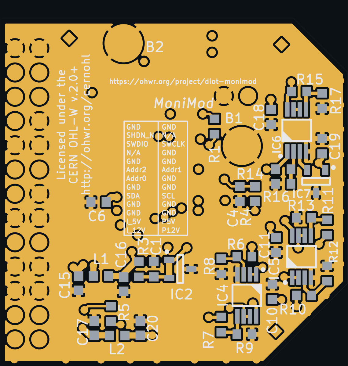
DIOT MONIMOD RATOPUS (OHWR0075 R1) is an open-hardware circuit board from the CERN Open Hardware Repository, designed in KiCad EDA: a 4-layer board of 36.3 × 36.3 mm with 58 components and 35 nets, published under CERN-OHL-W-2.0.
review 90% walked · 6 findings: 3 major · 3 minor (18 items)
Open in the interactive viewerRead the full review
Design review
Probe recorded 6 findings: 3 major · 3 minor (18 items) on this design. Each is shown here with its reasoning; the full review links every one to the pins, nets and datasheet pages it rests on.
IC3 3.3 V LDO: BOM orders TPS78633DCQ (pin 5 = NR) while the value says TPS7A4533DCQ (pin 5 = SENSE), and pin 5 is tied to the output
The 3.3 V regulator IC3 is two different parts at once: its BOM row orders MPN TPS78633DCQ, but its value (and the schematic symbol's label) is TPS7A4533DCQ. Pin 5 is wired to P3V3, which is correct for the TPS7A4533 (SENSE) and wrong for the TPS78633, whose pin 5 is the NR noise-reduction node of the internal reference. Built with the ordered part, the reference filter node is driven from the output.
Item TPS7A4533DCQ (value) TPS78633DCQ (MPN ordered) Source Pin 5 SENSE, tie to OUT for fixed versions NR: 'Noise-reduction pin for fixed versions only. An external bypass capacitor, connected to this terminal, in conjunction with an internal resistor, creates a low-pass filter' TPS7A45 DS p3; TPS786 DS (SLVS389M) p3 Pin 1 SHDN EN same Max VIN 20 V 5.5 V TPS786 DS p6 Min COUT 10 uF ceramic 1 uF ceramic TPS7A45 DS p3; TPS786 DS p1 On this board pin 5 = P3V3 (OUT), pin 1 = /Connectors/shdn_n (R5 10k to P5V, host can pull low on J1 pin 24), IN = P5V netlist The schematic symbol (sheet 3, 'Power regulators') prints TPS786 pin names (EN, NR) with a TPS7A4533DCQ value, so the drawing itself carries both identities. The sibling board OHWR0073 DIOT MONIMOD orders TPS7A4533DCQ for the same circuit; OHWR0074 FANTRAY has the same mismatch (OBS-500). With TPS7A4533 fitted the wiring is right and the output capacitance (C14 + C15 10 uF + C6/C13 1 uF + 2 x 100 nF, about 12 uF effective after DC-bias derating) meets its 10 uF minimum.
Which part is meant needs settling in the BOM before the next build.
- ReferencePlaneDiscontinuitymajorOpen
'/Connectors/con_swdio' runs ALONG the split between the GND and P3V3 planes on IN2.CU at 1 place, the longest 4.7 mm; the impedance there is not said (fastest: /Connectors/con_swdio at 100 ps 10-90 %, ASSUMED)
On IN2.CU the GND and P3V3 planes part, and '/Connectors/con_swdio' runs down the slot between them at 1 place(s), rather than across it. This is not a crossing: the return still follows the track, in the plane on its other side and in the slot's edges, so it does not detour. What changes is the track's own impedance. With the plane gone from under it on this side for that length, its field reaches further, to the slot's edges and to the next plane beyond, so its capacitance falls and its impedance rises; every edge travelling down it is partly reflected where it enters the stretch and again where it leaves, by (Z2 - Z1)/(Z2 + Z1). The longer the stretch against the edge's rise, the more of the edge sees the full step. A crossing is generally the worse fault; a mismatch is not free. At 1 place(s) the impedance cannot be said: the slot's two edges were not both read beside the track. No place stays within 10 %, the tolerance controlled impedance is commonly built to (the stackup states none), so the finding is a warning. One decision covers the split line's slot: whether these tracks may run down it, or should be moved over solid plane.
- '/Connectors/con_swdio' on IN1.CU at (141.39, -108.54), 6.68 mm, running ALONG the split for 4.7 mm, not across it, impedance not said: the slot's two edges were not both read beside the track; other side: GND on F.CU, 0.48 mm from the track against 0.48 mm to IN2.CU: 50% of the return on IN2.CU
Every site is a row of this finding's evidence, keyed by net, layers and position. GET /api/odb/boards/76/reference-planes?group=along%40IN2.CU%3AGND%7CP3V3 serves each with its own layer_image region; all of them lie in x 139.21..142.39, y -112.51..-103.88 mm (board frame, Y up).
Read from the copper as drawn on the reference layer, along each track's centreline at exact breakpoints. The reference is the copper beside the track, never the layer's type or name. Whether it matters depends on each signal's edge rate, which nothing on file states for these nets: a slow static line crosses a split harmlessly, a fast edge does not.
At along@IN2.CU:GND|P3V3
- PartLifecyclemajorOpen
PartLifecycle: 2 part numbers×2
2 Obsolete · on 2 placements
At IC7, Q1
Each finding, with its own headline
IC7LM45CIM3/NOPB on IC7: the distributor catalogue reports "Obsolete" for Texas Instruments's LM45CIM3/NOPB
LM45CIM3/NOPB on IC7: the distributor catalogue reports "Obsolete" for Texas Instruments's LM45CIM3/NOPB — a sourcing/longevity risk to confirm against the MANUFACTURER before acting. That is the maker this board's BOM names (TEXAS INSTRUMENTS). A distributor delisting is not the same claim as the part being unavailable; check the vendor's own lifecycle/product-change notice for the status and any named successor. Re-read the source: GET /api/odb/parts/LM45CIM3/NOPB/providers (which provider said it, the maker and part number it matched, its own words, and when we asked). THE LAST BUY DATE HAS PASSED (2024-02-09, 1,010 day(s) ago), so this is a substitution rather than a buy. The distributor reports NONE left. No approved alternate is recorded for this position.
Q17A-8.000MAAE-T on Q1: the distributor catalogue reports "Obsolete" for TXC CORPORATION's 7A-8.000MAAE-T
7A-8.000MAAE-T on Q1: the distributor catalogue reports "Obsolete" for TXC CORPORATION's 7A-8.000MAAE-T — a sourcing/longevity risk to confirm against the MANUFACTURER before acting. That is the maker this board's BOM names (TXC CORPORATION). A distributor delisting is not the same claim as the part being unavailable; check the vendor's own lifecycle/product-change notice for the status and any named successor. Re-read the source: GET /api/odb/parts/7A-8.000MAAE-T/providers (which provider said it, the maker and part number it matched, its own words, and when we asked). THE LAST BUY DATE HAS PASSED (2021-09-30, 1,872 day(s) ago), so this is a substitution rather than a buy. The distributor reports NONE left. No approved alternate is recorded for this position.
ADC reference IC2 (TL431) runs at 0.40 mA, below its 1 mA minimum, with 100 nF on its cathode inside the TL431 oscillation band
Vref25, the MCU's ADC reference (IC1 PA03/VREFA), comes from IC2 TL431B biased by R3 = 2 k from P3V3_AUX: (3.3 - 2.495) / 2 k = 0.40 mA, below the 1 mA minimum operating cathode current. C1 = 100 nF directly on the cathode is inside the region Nexperia's Fig. 17 marks as oscillation at low cathode current.
Quantity Value Source Bias resistor R3 2 k, P3V3_AUX to Vref25 netlist Cathode current available 0.40 mA computed Recommended cathode current 1 mA min Nexperia TL431 Rev. 8, Table 8, p6 I_K(min) TL431B 0.4 typ, 0.6 max mA Table 10, p8 Load capacitance C1 100 nF netlist / BOM Oscillation band at low IK about 5 nF to 350 nF Fig. 17, p12 (typical) The only other load is IC1's VREFA input, so the reference may sit at its nominal voltage, but it is out of its rated operating range and its accuracy is not specified there. The same circuit is OBS-494/495 on OHWR0073 DIOT MONIMOD and OBS-501 on OHWR0074 FANTRAY. A bias of about 1-2 mA (R3 about 470 R) and a capacitor outside the band would fix it.
Analog buffers IC4-IC6 on always-on +5VA drive the SAMD21's ADC pins while shdn_n holds its P3V3 off
While the crate holds shdn_n low, the three OPA2192 buffers (IC4-IC6) stay powered from +5VA and keep driving the ADC pins of the unpowered SAMD21 (IC1).
Power domains
Rail Source Switched? Source of fact P5V J1 (from the RaToPUS) always on power tree, root at J1 +5VA P5V through L2 always on power tree edge P5V -> +5VA via L2 P3V3 IC3 TPS78633 LDO from P5V EN = shdn_n (J1.24, R5) IC3 pin 1 on /Connectors/shdn_n What crosses them
IC4/IC5 (OPA2192, supply pin 8 = +5VA) drive /Analog/12V_Vsense_ADC, /Analog/12V_Isense_ADC, /Analog/5V_Vsense_ADC and /Analog/5V_Isense_ADC, and IC6 drives /Analog/T_ADC; all five land on IC1 ATSAMD21G18A, a 3.3 V part on P3V3. With shdn_n low, P3V3 is off while the buffers still output their divided measurement voltages into IC1's ADC pins, back-feeding it through its input protection.
Ask
CERN is asked to confirm the buffers' outputs stay inside IC1's limits with IC1 unpowered, or to switch +5VA with P3V3. The same arrangement on OHWR0074 R4 DIOT MONIMOD FANTRAY is OBS-586.
- ReferencePlaneDiscontinuityminorOpen
ReferencePlaneDiscontinuity: 12 boards×12
Checked by the review, stands · Claude walker W1 (Cern session) — Checked: the splits, voids and reference changes are read from the copper and stand as reported. They sit on slow monitoring, I2C, SWD and shutdown nets of a 48 MHz microcontroller board; no datasheet or app note on file sets a limit for them, and the reported impedance excursions are about 2 %. Not refutable with a citation; left for the owner.
At along@IN2.CU:+5VA|P3V3, refchange:+5VA|GND, refchange:GND|P3V3, split@IN2.CU:+5VA|P3V3, split@IN2.CU:GND|P3V3, void:GND@F.CU:122.8,-110.88 and 6 more
Each finding, with its own headline
along@IN2.CU:+5VA|P3V3'P12V' runs ALONG the split between the +5VA and P3V3 planes on IN2.CU at 1 place, the longest 3.55 mm; the impedance rises from 55 ohm to 57 ohm there at worst, 1.9 % of each edge reflected (fastest: P12V at 20 ns 10-90 %, suggested by its name)
On IN2.CU the +5VA and P3V3 planes part, and 'P12V' runs down the slot between them at 1 place(s), rather than across it. This is not a crossing: the return still follows the track, in the plane on its other side and in the slot's edges, so it does not detour. What changes is the track's own impedance. With the plane gone from under it on this side for that length, its field reaches further, to the slot's edges and to the next plane beyond, so its capacitance falls and its impedance rises; every edge travelling down it is partly reflected where it enters the stretch and again where it leaves, by (Z2 - Z1)/(Z2 + Z1). The longer the stretch against the edge's rise, the more of the edge sees the full step. A crossing is generally the worse fault; a mismatch is not free. Over solid plane each track is 55 ohm; along the slot 57 ohm, reflecting up to 1.9 % of each edge (a method-of-moments field solve of the cross-section, one dielectric; were the slot's edges to carry none of the return, up to 63 ohm). At every place the rise is within 10 %, the tolerance controlled impedance is commonly built to (the stackup states none), so the finding is the lower tier (info). One decision covers the split line's slot: whether these tracks may run down it, or should be moved over solid plane.
- 'P12V' on IN1.CU at (147.02, -123.7), 6.31 mm, running ALONG the split for 3.55 mm, not across it, 55 ohm over solid plane, 57 ohm along it: 1.9 % of each edge reflected; other side: GND on F.CU, 0.48 mm from the track against 0.48 mm to IN2.CU: 50% of the return on IN2.CU
Every site is a row of this finding's evidence, keyed by net, layers and position. GET /api/odb/boards/76/reference-planes?group=along%40IN2.CU%3A%2B5VA%7CP3V3 serves each with its own layer_image region; all of them lie in x 143.48..150.56, y -125.46..-121.33 mm (board frame, Y up).
Read from the copper as drawn on the reference layer, along each track's centreline at exact breakpoints. The reference is the copper beside the track, never the layer's type or name. Whether it matters depends on each signal's edge rate, which nothing on file states for these nets: a slow static line crosses a split harmlessly, a fast edge does not.
refchange:+5VA|GND'/Analog/5V_Isense_ADC' changes reference between +5VA and GND at a via, each with another reference that continues across (fastest: /Analog/5V_Isense_ADC at 20 ns 10-90 %, suggested by its name)
At 1 via(s), on 1 net(s), the signal leaves a layer referenced by one of +5VA and GND for a layer referenced by the other, and no plane references both layers. Different nets: no via can carry the return across; only decoupling between the two planes near the via can. The capacitor carrying the return across was measured at each via, at the knee of the crossing net's edge against 50 ohm assumed: 1 with none. 1 of them at an ASSUMED edge (no edge on file for the net): state one (net_timing_state) and it is re-read. One decision covers the pair: whether +5VA and GND are decoupled to each other near these vias. A via whose layers have more references than these two is a site of each pair it joins. Every one is partial: another reference continues across through a stitching via of its net, so only part of the return has nowhere to go, and the finding is the lower tier (info). They are listed with the farthest stitching via first.
- '/Analog/5V_Isense_ADC' at (153.57, -119.48), F.CU -> IN1.CU: GND on IN1.CU to GND on F.CU, +5VA on IN2.CU; partial, GND continues through a via of GND 1.29 mm away; stitching none, 16.5 mm of track past the via on IN1.CU: At the 5 GHz knee of a 100 ps edge (20 ns 10-90 %, assumed: no edge is on file for the net) no capacitor carries the return; only the planes do. +5VA and GND are not a thin pair (at most 0.2 mm), so their own capacitance does not carry the return. To serve it, change layers across the same plane, or move the signal to a layer referenced to ground. Measured for reference: C11 (100 nF 0603) 2.3 mm away: 0.56 nH in the 0.480 mm cavity + 0.51 nH ESL + 0.68 nH mounting (pad 0.10 nH + no via of the first net within 1 mm of its pad: the study's 0.6 nH per mm of 0.96 mm depth, ASSUMED): 54.8 ohm at the knee, 110 % of 50 ohm (assumed track impedance). None.
Every site is a row of this finding's evidence, keyed by net, layers and position. GET /api/odb/boards/76/reference-planes?group=refchange%3A%2B5VA%7CGND serves each with its own layer_image region; all of them lie in x 151.57..155.57, y -121.48..-117.48 mm (board frame, Y up).
The reference on each layer is the first plane the track meets leaving the via, anti-pads and the net's own copper skipped. Whether it matters depends on each signal's edge rate, which nothing on file states for these nets: a slow static line crosses a split harmlessly, a fast edge does not.
refchange:GND|P3V33 nets change reference between GND and P3V3 at 3 vias, each with another reference that continues across (fastest: /Analog/T_ADC at 100 ps 10-90 %, ASSUMED)
At 3 via(s), on 3 net(s), the signal leaves a layer referenced by one of GND and P3V3 for a layer referenced by the other, and no plane references both layers. Different nets: no via can carry the return across; only decoupling between the two planes near the via can. The capacitor carrying the return across was measured at each via, at the knee of the crossing net's edge against 50 ohm assumed: 3 with none. 3 of them at an ASSUMED edge (no edge on file for the net): state one (net_timing_state) and it is re-read. One decision covers the pair: whether GND and P3V3 are decoupled to each other near these vias. A via whose layers have more references than these two is a site of each pair it joins. Every one is partial: another reference continues across through a stitching via of its net, so only part of the return has nowhere to go, and the finding is the lower tier (info). They are listed with the farthest stitching via first.
- '/Analog/5V_Vsense_ADC' at (152.1, -122.53), F.CU -> IN1.CU: GND on IN1.CU to GND on F.CU, P3V3 on IN2.CU; partial, GND continues through a via of GND 2.1 mm away; stitching none, 17.1 mm of track past the via on IN1.CU: At the 5 GHz knee of a 100 ps edge (20 ns 10-90 %, assumed: no edge is on file for the net) no capacitor carries the return; only the planes do. GND and P3V3 are not a thin pair (at most 0.2 mm), so their own capacitance does not carry the return. To serve it, change layers across the same plane, or move the signal to a layer referenced to ground. None.
- '/Analog/T_ADC' at (150.27, -111.25), F.CU -> IN1.CU: GND on IN1.CU to GND on F.CU, P3V3 on IN2.CU; partial, GND continues through a via of GND 1.25 mm away; stitching none, 13.3 mm of track past the via on IN1.CU: At the 5 GHz knee of a 100 ps edge (100 ps 10-90 %, assumed: no edge is on file for the net) no capacitor carries the return; only the planes do. GND and P3V3 are not a thin pair (at most 0.2 mm), so their own capacitance does not carry the return. To serve it, change layers across the same plane, or move the signal to a layer referenced to ground. None.
- '/uC/m_scl' at (134.62, -115.57), IN1.CU -> B.CU: GND on F.CU, P3V3 on IN2.CU to GND on IN2.CU; partial, GND continues through a via of GND 1.12 mm away; stitching none, 1.5 mm of track past the via on B.CU: At the 5 GHz knee of a 100 ps edge (10 ns 10-90 %, assumed: no edge is on file for the net) no capacitor carries the return; only the planes do. GND and P3V3 are not a thin pair (at most 0.2 mm), so their own capacitance does not carry the return. To serve it, change layers across the same plane, or move the signal to a layer referenced to ground. Measured for reference: C6 (1 uF 0603) 2.1 mm away: 1.08 nH in the 0.960 mm cavity + 0.51 nH ESL + 0.68 nH mounting (pad 0.10 nH + no via of the first net within 1 mm of its pad: the study's 0.6 nH per mm of 0.96 mm depth, ASSUMED): 71.1 ohm at the knee, 142 % of 50 ohm (assumed track impedance). None.
Every site is a row of this finding's evidence, keyed by net, layers and position. GET /api/odb/boards/76/reference-planes?group=refchange%3AGND%7CP3V3 serves each with its own layer_image region; all of them lie in x 132.62..154.1, y -124.53..-109.25 mm (board frame, Y up).
The reference on each layer is the first plane the track meets leaving the via, anti-pads and the net's own copper skipped. Whether it matters depends on each signal's edge rate, which nothing on file states for these nets: a slow static line crosses a split harmlessly, a fast edge does not.
split@IN2.CU:+5VA|P3V32 nets cross the split between the +5VA and P3V3 planes on IN2.CU at 2 places, all with a plane on the track's other side (fastest: /Analog/12V_Isense_ADC at 20 ns 10-90 %, suggested by its name)
On IN2.CU the +5VA and P3V3 planes part, and 2 nets cross from one to the other at 2 place(s). The return current cannot follow a track across; it detours to wherever the two planes are joined (a stitching capacitor, or the source), and the loop it opens radiates and couples. One decision covers the boundary: whether it is stitched near these crossings, or the nets crossing it are slow enough not to care. Tracks that run ALONG this split, down the slot rather than across it, are a finding of their own: theirs is an impedance step, not a detour. At 2 of the 2 crossing(s) the track's other neighbour carries a plane, which the return can use there. Every crossing has a plane on the track's other side at most twice as far away as the broken one, so at most 50% of the return meets the break and the rest follows the track on that plane (to first order each plane beside a stripline carries a share of the return inversely proportional to its distance from the track). The finding is the lower tier (info).
- '/Analog/12V_Isense_ADC' on IN1.CU at (144.67, -124.04), 2.72 mm; other side: GND on F.CU, 0.48 mm from the track against 0.48 mm to IN2.CU: 50% of the return on IN2.CU
- '/Analog/5V_Isense_ADC' on IN1.CU at (150.56, -116.48), 1.13 mm; other side: GND on F.CU, 0.48 mm from the track against 0.48 mm to IN2.CU: 50% of the return on IN2.CU
Every site is a row of this finding's evidence, keyed by net, layers and position. GET /api/odb/boards/76/reference-planes?group=split%40IN2.CU%3A%2B5VA%7CP3V3 serves each with its own layer_image region; all of them lie in x 142.66..152.18, y -125.46..-115.48 mm (board frame, Y up).
Read from the copper as drawn on the reference layer, along each track's centreline at exact breakpoints. The reference is the copper beside the track, never the layer's type or name. Whether it matters depends on each signal's edge rate, which nothing on file states for these nets: a slow static line crosses a split harmlessly, a fast edge does not.
split@IN2.CU:GND|P3V310 nets cross the split between the GND and P3V3 planes on IN2.CU at 12 places, all with a plane on the track's other side (fastest: /Analog/T_ADC at 100 ps 10-90 %, ASSUMED)
On IN2.CU the GND and P3V3 planes part, and 10 nets cross from one to the other at 12 place(s). The return current cannot follow a track across; it detours to wherever the two planes are joined (a stitching capacitor, or the source), and the loop it opens radiates and couples. One decision covers the boundary: whether it is stitched near these crossings, or the nets crossing it are slow enough not to care. Tracks that run ALONG this split, down the slot rather than across it, are a finding of their own: theirs is an impedance step, not a detour. At 12 of the 12 crossing(s) the track's other neighbour carries a plane, which the return can use there. Every crossing has a plane on the track's other side at most twice as far away as the broken one, so at most 50% of the return meets the break and the rest follows the track on that plane (to first order each plane beside a stripline carries a share of the return inversely proportional to its distance from the track). The finding is the lower tier (info).
- '/Analog/12V_Isense_ADC' on IN1.CU at (143.66, -120.45), 0.21 mm; other side: GND on F.CU, 0.48 mm from the track against 0.48 mm to IN2.CU: 50% of the return on IN2.CU
- '/Analog/12V_Vsense_ADC' on IN1.CU at (146.55, -118.68), 0.41 mm; other side: GND on F.CU, 0.48 mm from the track against 0.48 mm to IN2.CU: 50% of the return on IN2.CU
- '/Analog/5V_Isense_ADC' on IN1.CU at (147.17, -116.48), 0.3 mm; other side: GND on F.CU, 0.48 mm from the track against 0.48 mm to IN2.CU: 50% of the return on IN2.CU
- '/Analog/5V_Vsense_ADC' on IN1.CU at (147.17, -117.14), 0.3 mm; other side: GND on F.CU, 0.48 mm from the track against 0.48 mm to IN2.CU: 50% of the return on IN2.CU
- '/Analog/T_ADC' on IN1.CU at (147.2, -115.44), 0.51 mm; other side: GND on F.CU, 0.48 mm from the track against 0.48 mm to IN2.CU: 50% of the return on IN2.CU
- '/Connectors/con_swclk' on IN1.CU at (143.68, -109.96), 3.67 mm; other side: GND on F.CU, 0.48 mm from the track against 0.48 mm to IN2.CU: 50% of the return on IN2.CU
- '/Connectors/con_swclk' on IN1.CU at (145.45, -101.79), 2.02 mm; other side: GND on F.CU, 0.48 mm from the track against 0.48 mm to IN2.CU: 50% of the return on IN2.CU
- '/Connectors/con_swdio' on IN1.CU at (144.01, -101.66), 2.17 mm; other side: GND on F.CU, 0.48 mm from the track against 0.48 mm to IN2.CU: 50% of the return on IN2.CU
- '/Connectors/pgm_rst_n' on IN1.CU at (147.07, -103.35), 2.95 mm; other side: GND on F.CU, 0.48 mm from the track against 0.48 mm to IN2.CU: 50% of the return on IN2.CU
- '/uC/m_sda' on IN1.CU at (133.5, -117.47), 0.3 mm; other side: GND on F.CU, 0.48 mm from the track against 0.48 mm to IN2.CU: 50% of the return on IN2.CU
- 'P12V' on IN1.CU at (144.48, -120.45), 0.21 mm; other side: GND on F.CU, 0.48 mm from the track against 0.48 mm to IN2.CU: 50% of the return on IN2.CU
- 'P12V' on IN1.CU at (145.85, -119.38), 0.4 mm; other side: GND on F.CU, 0.48 mm from the track against 0.48 mm to IN2.CU: 50% of the return on IN2.CU
Every site is a row of this finding's evidence, keyed by net, layers and position. GET /api/odb/boards/76/reference-planes?group=split%40IN2.CU%3AGND%7CP3V3 serves each with its own layer_image region; all of them lie in x 132.35..148.32, y -121.55..-99.36 mm (board frame, Y up).
Read from the copper as drawn on the reference layer, along each track's centreline at exact breakpoints. The reference is the copper beside the track, never the layer's type or name. Whether it matters depends on each signal's edge rate, which nothing on file states for these nets: a slow static line crosses a split harmlessly, a fast edge does not.
void:GND@F.CU:122.8,-110.88'/Connectors/shdn_n' crosses where the outline of the GND plane on F.CU is drawn back, at 1 place, the longest 17.54 mm (fastest: /Connectors/shdn_n at 20 ns 10-90 %, suggested by its name)
Along '/Connectors/shdn_n' on IN1.CU, the GND plane on F.CU has 17.54 mm under the track with no copper, at (122.8, -110.88), the same plane on both sides. No single drill's anti-pad and no landing explains it: a clearance is excused only when it holds a drill and is drawn round it, or the track ends in it on the net's own pad or via, or runs through its own via's clearance and no farther. The return current detours round the void. 1 of them run ALONG the bare copper, parallel to its edges, rather than across it (the longest 7.46 mm). No hole cleared it: the outline of the pour at x 122.93..158.25, y -131.33..-96 is drawn back there. One decision covers the void: whether these tracks may cross it, or the plane should be filled under them. No crossing has a plane on the track's other side, so the whole return meets the break.
- '/Connectors/shdn_n' on IN1.CU at (122.8, -110.88), 17.54 mm, running ALONG the bare copper for 7.46 mm, not across it over no copper; other side: no plane on IN2.CU
Every site is a row of this finding's evidence, keyed by net, layers and position. GET /api/odb/boards/76/reference-planes?group=void%3AGND%40F.CU%3A122.8%2C-110.88 serves each with its own layer_image region; all of them lie in x 121.8..123.93, y -120.59..-101.16 mm (board frame, Y up).
Read from the copper as drawn on the reference layer, along each track's centreline at exact breakpoints. The reference is the copper beside the track, never the layer's type or name. Whether it matters depends on each signal's edge rate, which nothing on file states for these nets: a slow static line crosses a split harmlessly, a fast edge does not.
void:GND@F.CU:144.27,-107.62'/Connectors/con_swclk' crosses where the outline of the GND plane on F.CU is drawn back, at 1 place, the longest 1.96 mm (fastest: /Connectors/con_swclk at 1 ns 10-90 %, suggested by its name)
Along '/Connectors/con_swclk' on IN1.CU, the GND plane on F.CU has 1.96 mm under the track with no copper, at (144.27, -107.62), running to the end of the track. No single drill's anti-pad and no landing explains it: a clearance is excused only when it holds a drill and is drawn round it, or the track ends in it on the net's own pad or via, or runs through its own via's clearance and no farther. The return current detours round the void. 1 of them run ALONG the bare copper, parallel to its edges, rather than across it (the longest 0.68 mm). No hole cleared it: the outline of the pour at x 122.93..158.25, y -131.33..-96 is drawn back there. One decision covers the void: whether these tracks may cross it, or the plane should be filled under them. Every crossing has a plane on the track's other side at most twice as far away as the broken one, so at most 50% of the return meets the break and the rest follows the track on that plane (to first order each plane beside a stripline carries a share of the return inversely proportional to its distance from the track). The finding is the lower tier (info).
- '/Connectors/con_swclk' on IN1.CU at (144.27, -107.62), 1.96 mm, running ALONG the bare copper for 0.68 mm, not across it over no copper, to the end of the track; other side: P3V3 on IN2.CU, 0.48 mm from the track against 0.48 mm to F.CU: 50% of the return on F.CU
Every site is a row of this finding's evidence, keyed by net, layers and position. GET /api/odb/boards/76/reference-planes?group=void%3AGND%40F.CU%3A144.27%2C-107.62 serves each with its own layer_image region; all of them lie in x 143.27..145.27, y -110.31..-105.94 mm (board frame, Y up).
Read from the copper as drawn on the reference layer, along each track's centreline at exact breakpoints. The reference is the copper beside the track, never the layer's type or name. Whether it matters depends on each signal's edge rate, which nothing on file states for these nets: a slow static line crosses a split harmlessly, a fast edge does not.
void:GND@F.CU:copper of /Connectors/con_swclk'/Connectors/pgm_rst_n' crosses where the GND plane on F.CU is drawn back round copper of /Connectors/con_swclk, at 1 place, the longest 1.23 mm (fastest: /Connectors/pgm_rst_n at 20 ns 10-90 %, suggested by its name)
Along '/Connectors/pgm_rst_n' on IN1.CU, the GND plane on F.CU has 1.23 mm under the track with copper of /Connectors/con_swclk, not a plane, at (145.14, -107.81), the same plane on both sides. No single drill's anti-pad and no landing explains it: a clearance is excused only when it holds a drill and is drawn round it, or the track ends in it on the net's own pad or via, or runs through its own via's clearance and no farther. The return current detours round the void. No hole cleared it: the outline of the pour at x 122.93..158.25, y -131.33..-96 is drawn back there. One decision covers the void: whether these tracks may cross it, or the plane should be filled under them. Every crossing has a plane on the track's other side at most twice as far away as the broken one, so at most 50% of the return meets the break and the rest follows the track on that plane (to first order each plane beside a stripline carries a share of the return inversely proportional to its distance from the track). The finding is the lower tier (info).
- '/Connectors/pgm_rst_n' on IN1.CU at (145.14, -107.81), 1.23 mm over copper of /Connectors/con_swclk, not a plane; other side: P3V3 on IN2.CU, 0.48 mm from the track against 0.48 mm to F.CU: 50% of the return on F.CU
Every site is a row of this finding's evidence, keyed by net, layers and position. GET /api/odb/boards/76/reference-planes?group=void%3AGND%40F.CU%3Acopper%20of%20%2FConnectors%2Fcon_swclk serves each with its own layer_image region; all of them lie in x 144.14..146.53, y -109.27..-106.2 mm (board frame, Y up).
Read from the copper as drawn on the reference layer, along each track's centreline at exact breakpoints. The reference is the copper beside the track, never the layer's type or name. Whether it matters depends on each signal's edge rate, which nothing on file states for these nets: a slow static line crosses a split harmlessly, a fast edge does not.
void:GND@IN1.CU:153.35,-122.51'/Connectors/5V_Imeas' crosses where the outline of the GND plane on IN1.CU is drawn back, at 1 place, the longest 2.36 mm (fastest: /Connectors/5V_Imeas at 20 ns 10-90 %, suggested by its name)
Along '/Connectors/5V_Imeas' on IN2.CU, the GND plane on IN1.CU has 2.36 mm under the track with no copper, at (153.35, -122.51), the same plane on both sides. No single drill's anti-pad and no landing explains it: a clearance is excused only when it holds a drill and is drawn round it, or the track ends in it on the net's own pad or via, or runs through its own via's clearance and no farther. The return current detours round the void. 1 of them run ALONG the bare copper, parallel to its edges, rather than across it (the longest 1.67 mm). No hole cleared it: the outline of the pour at x 148.18..158.25, y -128.98..-96.37 is drawn back there. One decision covers the void: whether these tracks may cross it, or the plane should be filled under them. Every crossing has a plane on the track's other side at most twice as far away as the broken one, so at most 50% of the return meets the break and the rest follows the track on that plane (to first order each plane beside a stripline carries a share of the return inversely proportional to its distance from the track). The finding is the lower tier (info).
- '/Connectors/5V_Imeas' on IN2.CU at (153.35, -122.51), 2.36 mm, running ALONG the bare copper for 1.67 mm, not across it over no copper; other side: GND on B.CU, 0.48 mm from the track against 0.48 mm to IN1.CU: 50% of the return on IN1.CU
Every site is a row of this finding's evidence, keyed by net, layers and position. GET /api/odb/boards/76/reference-planes?group=void%3AGND%40IN1.CU%3A153.35%2C-122.51 serves each with its own layer_image region; all of them lie in x 151.51..155.18, y -124.34..-120.67 mm (board frame, Y up).
Read from the copper as drawn on the reference layer, along each track's centreline at exact breakpoints. The reference is the copper beside the track, never the layer's type or name. Whether it matters depends on each signal's edge rate, which nothing on file states for these nets: a slow static line crosses a split harmlessly, a fast edge does not.
void:P3V3@IN2.CU:147.65,-114.02'/Analog/T_ADC' crosses where the outline of the P3V3 plane on IN2.CU is drawn back, at 1 place, the longest 0.67 mm (fastest: /Analog/T_ADC at 100 ps 10-90 %, ASSUMED)
Along '/Analog/T_ADC' on IN1.CU, the P3V3 plane on IN2.CU has 0.67 mm under the track with no copper, at (147.65, -114.02), the same plane on both sides. No single drill's anti-pad and no landing explains it: a clearance is excused only when it holds a drill and is drawn round it, or the track ends in it on the net's own pad or via, or runs through its own via's clearance and no farther. The return current detours round the void. No hole cleared it: the outline of the pour at x 133.3..150.16, y -122.33..-102.11 is drawn back there. One decision covers the void: whether these tracks may cross it, or the plane should be filled under them. Every crossing has a plane on the track's other side at most twice as far away as the broken one, so at most 50% of the return meets the break and the rest follows the track on that plane (to first order each plane beside a stripline carries a share of the return inversely proportional to its distance from the track). The finding is the lower tier (info).
- '/Analog/T_ADC' on IN1.CU at (147.65, -114.02), 0.67 mm over no copper; other side: GND on F.CU, 0.48 mm from the track against 0.48 mm to IN2.CU: 50% of the return on IN2.CU
Every site is a row of this finding's evidence, keyed by net, layers and position. GET /api/odb/boards/76/reference-planes?group=void%3AP3V3%40IN2.CU%3A147.65%2C-114.02 serves each with its own layer_image region; all of them lie in x 146.47..148.93, y -115.26..-112.84 mm (board frame, Y up).
Read from the copper as drawn on the reference layer, along each track's centreline at exact breakpoints. The reference is the copper beside the track, never the layer's type or name. Whether it matters depends on each signal's edge rate, which nothing on file states for these nets: a slow static line crosses a split harmlessly, a fast edge does not.
void:routed@F.CU|IN1.CU'/Connectors/con_swclk' on IN1.CU crosses the tracks routed through the GND pour on F.CU at 1 place, the longest 1.53 mm; 1 runs ALONG the cut round another net's track (fastest: /Connectors/con_swclk at 1 ns 10-90 %, suggested by its name)
The GND pour on F.CU is cleared round tracks routed through it, and tracks on IN1.CU, which take that pour as their reference, cross them: for the width of each cut the return has no plane under it and detours round the cut. 1 place(s) on 1 net(s). 1 of the crossings run ALONG the cut round another net's track rather than across it, parallel to its edges (the longest 0.78 mm): over or right beside that track, broadside to it as well as off the plane. One decision covers the layer pair: whether these layers may take a pour their own tracks cut as the reference, or the routing or the stackup should give the tracks a plane that is not cut where they cross. Every crossing has a plane on the track's other side at most twice as far away as the broken one, so at most 50% of the return meets the break and the rest follows the track on that plane (to first order each plane beside a stripline carries a share of the return inversely proportional to its distance from the track). The finding is the lower tier (info).
- '/Connectors/con_swclk' on IN1.CU at (144.48, -105.8), 1.53 mm, running ALONG the bare copper for 0.78 mm, not across it over copper of P3V3, not a plane; other side: P3V3 on IN2.CU, 0.48 mm from the track against 0.48 mm to F.CU: 50% of the return on F.CU
Every site is a row of this finding's evidence, keyed by net, layers and position. GET /api/odb/boards/76/reference-planes?group=void%3Arouted%40F.CU%7CIN1.CU serves each with its own layer_image region; all of them lie in x 143.27..145.48, y -107.62..-104.18 mm (board frame, Y up).
Read from the copper as drawn on the reference layer, along each track's centreline at exact breakpoints. The reference is the copper beside the track, never the layer's type or name. Whether it matters depends on each signal's edge rate, which nothing on file states for these nets: a slow static line crosses a split harmlessly, a fast edge does not.
void:routed@IN1.CU|IN2.CUTracks on IN1.CU and IN2.CU cross each other at 8 places, each layer the other's reference with its pour cleared round its own tracks, the longest 26.59 mm; 5 run ALONG the cut round another net's track (fastest: /Connectors/Addr0 at 100 ps 10-90 %, ASSUMED)
IN1.CU and IN2.CU each carry a pour and routed tracks, and each is the other's nearest reference. Wherever a track on one crosses a track on the other, the pour under it is cleared round that other track, so for the width of the cut the return has no plane under it and detours round the cut. 8 place(s) on 8 net(s), 1 of them seen from both tracks (each counted once). 5 of the crossings run ALONG the cut round another net's track rather than across it, parallel to its edges (the longest 15.79 mm): over or right beside that track, broadside to it as well as off the plane. One decision covers the layer pair: whether these layers may take a pour their own tracks cut as the reference, or the routing or the stackup should give the tracks a plane that is not cut where they cross. Every crossing has a plane on the track's other side at most twice as far away as the broken one, so at most 50% of the return meets the break and the rest follows the track on that plane (to first order each plane beside a stripline carries a share of the return inversely proportional to its distance from the track). The finding is the lower tier (info).
- one crossing of two tracks, seen from each: '/Connectors/12V_Imeas' on IN2.CU at (132.27, -129.98), 17.82 mm, running ALONG the bare copper for 13.75 mm, not across it over copper of P12V, not a plane, to the end of the track; other side: GND on B.CU, 0.48 mm from the track against 0.48 mm to IN1.CU: 50% of the return on IN1.CU / 'P12V' on IN1.CU at (142.62, -129.92), 26.59 mm, running ALONG the bare copper for 15.79 mm, not across it over copper of /Connectors/12V_Imeas, not a plane, to the end of the track; other side: GND on F.CU, 0.48 mm from the track against 0.48 mm to IN2.CU: 50% of the return on IN2.CU
- '/Connectors/con_swdio' on IN1.CU at (134.27, -102.45), 18.75 mm, running ALONG the bare copper for 8.72 mm, not across it over copper of P5V, not a plane, to the end of the track; other side: GND on F.CU, 0.48 mm from the track against 0.48 mm to IN2.CU: 50% of the return on IN2.CU
- '/Connectors/con_swclk' on IN1.CU at (134.16, -100.79), 13.62 mm, running ALONG the bare copper for 7.78 mm, not across it over copper of P5V, not a plane, to the end of the track; other side: GND on F.CU, 0.48 mm from the track against 0.48 mm to IN2.CU: 50% of the return on IN2.CU
- '/Connectors/Addr0' on IN2.CU at (128.93, -108.84), 12.69 mm over copper of P5V, not a plane, to the end of the track; other side: GND on B.CU, 0.48 mm from the track against 0.48 mm to IN1.CU: 50% of the return on IN1.CU
- '/Connectors/Addr2' on IN2.CU at (128.93, -106.05), 11.47 mm over copper of P5V, not a plane, to the end of the track; other side: GND on B.CU, 0.48 mm from the track against 0.48 mm to IN1.CU: 50% of the return on IN1.CU
- '/Connectors/Addr1' on IN2.CU at (129.31, -106.45), 8.8 mm over copper of P5V, not a plane, to the end of the track; other side: GND on B.CU, 0.48 mm from the track against 0.48 mm to IN1.CU: 50% of the return on IN1.CU
- '/Connectors/5V_Imeas' on IN2.CU at (148.15, -123.45), 7.45 mm, running ALONG the bare copper for 3.76 mm, not across it over copper of /Analog/12V_Isense_ADC, P12V, not a plane; other side: GND on B.CU, 0.48 mm from the track against 0.48 mm to IN1.CU: 50% of the return on IN1.CU
- '/Connectors/Addr0' on IN2.CU at (141.85, -110.77), 1.9 mm over copper of /Connectors/con_swdio, /Connectors/con_swclk, not a plane, to the end of the track; other side: GND on B.CU, 0.48 mm from the track against 0.48 mm to IN1.CU: 50% of the return on IN1.CU
Every site is a row of this finding's evidence, keyed by net, layers and position. GET /api/odb/boards/76/reference-planes?group=void%3Arouted%40IN1.CU%7CIN2.CU serves each with its own layer_image region; all of them lie in x 122.98..152.07, y -131.43..-99.36 mm (board frame, Y up).
Read from the copper as drawn on the reference layer, along each track's centreline at exact breakpoints. The reference is the copper beside the track, never the layer's type or name. Whether it matters depends on each signal's edge rate, which nothing on file states for these nets: a slow static line crosses a split harmlessly, a fast edge does not.
Main parts
| Part number | Maker | Description | Where |
|---|---|---|---|
| 640453-2 | TYCO ELECTRONICS | J3 | |
| 7A-8.000MAAE-T | TXC CORPORATION | Q1 | |
| ATSAMD21G18A-AF | MICROCHIP | IC1 | |
| FTS-105-02-F-DV | SAMTEC | J2 | |
| LM45CIM3/NOPB | TEXAS INSTRUMENTS | IC7 | |
| M20-7831342 | HARWIN | J1 | |
| TL431BQDBZ | NXP SEMICONDUCTORS | IC2 | |
| TPS78633DCQ | TEXAS INSTRUMENTS | IC3 | |
| PLATED_HOLE2.4_PAD4.0 | B1, B2 | ||
| OPA2192IDGK | TEXAS INSTRUMENTS | IC4, IC5, IC6 | |
| FIDUCIAL_TARGET_S100-200 | FTG1, FTG2, FTG3, FTG4, FTG5, FTG6 | ||
| R0603_1K_1%_0.1W_100PPM | GENERIC | R4 | |
| BLM18PG121SN1D | MURATA | L1, L2 | |
| CC0603_22PF_50V_5%_NP0 | GENERIC | C2, C3 | |
| R0603_2K_1%_0.1W_100PPM | GENERIC | R3, R8 | |
| CC0603_100NF_50V_10%_X5R | GENERIC | C7, C8, C9 | |
| CC0603_1uF_16V_10%_X7R | GENERIC | C13, C5, C6 | |
| R0603_16K_1%_0.1W_100PPM | GENERIC | R10, R11, R7 | |
| CC0603_100NF_50V_10%_X7R | GENERIC | C1, C10, C11, C18, C19, C4 | |
| CC0603_10UF_16V_20%_X5R | GENERIC | C12, C14, C15, C16, C17, C20 | |
| R0603_10K_1%_0.1W_100PPM | GENERIC | R1, R12, R13, R14, R15, R16 and 5 more |
About this design
- Design
- DIOT MONIMOD RATOPUS — OHWR0075 R1
- Designed in
- KiCad EDA
- Board
- 4 copper layers, 36.3 × 36.3 mm, 58 components, 35 nets
- Licence
- CERN-OHL-W-2.0
- Source
- https://gitlab.com/ohwr/project/diot-monimod at commit
4e7c8230d0e1 - Attribution
- CERN Open Hardware Repository, project ohwr/project/diot-monimod (commit 4e7c8230d0e14c7e6820d53feef058688390b835, 2025-04-10). Licence: CERN-OHL-W-2.0. Source: https://gitlab.com/ohwr/project/diot-monimod. This is a snapshot of the copy published on the OHWR GitLab pages (R1), not CERN's released record. CERN's source of truth is EDMS (https://edms.cern.ch), and the current release may be newer.
- Reviewed with
- Probe by E# (E-Sharp AB)