 Probe

DIOT PB LBK
OHWR0058 · revision R1
DIOT PB LBK (OHWR0058 R1) is an open-hardware circuit board from its public repository, designed in Altium Designer: a 6-layer board of 220 × 100 mm with 75 components and 210 nets, published under CERN-OHL-W-2.0, CERN-OHL-S-2.0.
review complete · 4 findings: 4 minor (22 items)
Open in the interactive viewerRead the full review
Design review
Probe recorded 4 findings: 4 minor (22 items) on this design. Each is shown here with its reasoning; the full review links every one to the pins, nets and datasheet pages it rests on.
Schematic title blocks do not identify this board: no project name, revision or sheet count, and sheet 3 still carries the DI/OT System Board title block
The three schematic sheets don't identify this board, and sheet 3 still carries another board's title block, with a title that names the wrong connectors.
Sheet Title block Problem 1 DIOT_Loopback.SchDoc "Top schematic" Project/Equipment, Document and Rev empty; "Sheet 1 of" with no total 2 CPCIS_Connectors_P1_P4_P6.SchDoc "CPCIS Connectors" same empty fields; "Sheet 10 of" with no total 3 Cpcis_connectors_P2_P3_P5.SchDoc "DI/OT System Board / CPCIS Connectors P4-P6", "Sheet 21 of 29", "EDA-xxxx", Rev 2, drawn 1.10.2019 reused System Board sheet; it actually holds P2, P3 and P5 (J5, J6, J31) The licence notes also point at other projects. Sheets 1 and 2 give the source location https://www.ohwr.org/project/diot-pfc-ku and ask for it on the silkscreen of "a DI/OT FMC Carrier PCB"; sheet 3 gives diot-sb-zu.
Why it matters
For a published design, a reader can't tell from the drawings which board, which revision or how many sheets they have. The P4-P6 title on the P2/P3/P5 sheet could send someone to the wrong connector.
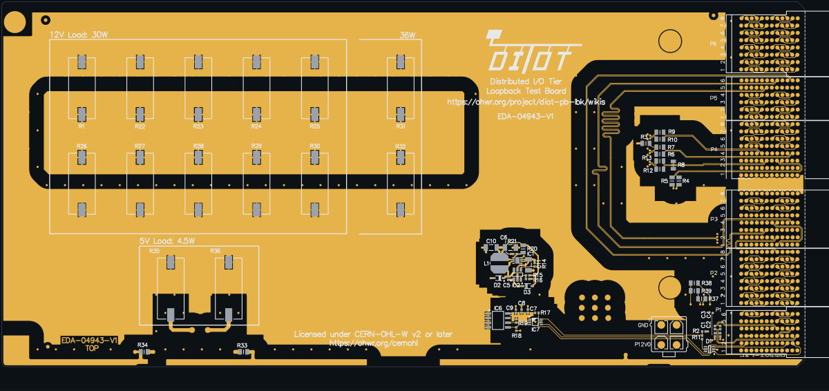
Stand-alone 12 V connector J4 has no designator on the silkscreen, and the six backplane connectors are marked P1-P6 rather than their BOM designators
The stand-alone 12 V connector J4 has no designator on the silkscreen, and the six backplane connectors are marked with their slot names P1-P6 instead of their BOM designators.
J4
J4 (Molex 39-28-1043, the stand-alone 12 V power input, at about x 182.8 / y 8.8 mm) is outlined on the top silkscreen with pin numbers 1 and 4 and net texts 'GND' and 'P12V0', but no 'J4'.
The CompactPCI Serial connectors
BOM designator Silkscreen Placement y (mm) J1 P1 9.5 J5 P2 24.5 J6 P3 40.5 J2 P4 59.5 J31 P5 73.5 J3 P6 88.5 The schematic uses the same P-names under each connector symbol, so the mapping can be worked out from the drawings. But the BOM, the pick-and-place data and any rework or inspection note use J1/J2/J3/J5/J6/J31/J4, and the board does not show those names.
Every other placed part checked carries a legible designator: text cap height about 1.0 mm, stroke about 0.2 mm, measured on the layer render at 100 px/mm.
Suggested fix: add 'J4', and the J designators next to the P names (e.g. 'J1/P1').
SERVMOD has a 200 R pull-down (R2) on the loopback board while the system board drives it from an MPSoC pin: about 16.5 mA to hold the PCA9306 enable high
SERVMOD, the system board's per-slot service-mode line, is pulled to GND on this board by R2 = 200 R, and the system board drives it straight from an MPSoC pin: holding it high (3.3 V) to enable the PCA9306 I2C switch IC7 asks about 16.5 mA of that pin.
Point Value Source SERVMOD pull-down R2 200 R to GND (fitted) this board's netlist and BOM; schematic sheet 2 What SERVMOD enables IC7 PCA9306 EN (switch configuration, VREF2 via R17 200 k) netlist; TI PCA9306 Fig. 8-5 Contact J1 K2 through R11 22 R (PESD3V3L5UY D1 on K2) netlist Far end (system slot, slot 1) OHWR0083 R5 DIOT SB ZU: 1_SERVMOD = MPSoC IC52 ball B1, no buffer Probe netlists, backplane OHWR0084 R3 J11_Slot1.K2 to system slot J5.C5 Load at 3.3 V 3.3 V / 200 R = 16.5 mA (plus 22 R in series) computed Question for CERN
Is the 200 R deliberate, as a test load on SERVMOD for this loopback board, and is the system-board pin configured for that drive? An LVCMOS 3.3 V FPGA output is normally set for a few mA to 12 mA; at 16.5 mA its high level sags and the pin runs above its configured drive. If the intent is only a defined low when nobody drives SERVMOD, a 10 k pull-down would do it.
- ReferencePlaneDiscontinuityminorOpen
ReferencePlaneDiscontinuity: 19 boards×19
Checked by the review, stands · Claude walker V2 (cern-01 session) — Post-0.529.0 verify, 19 findings, all lower tier (info), on the PCIe reference-clock pairs 4_PE_CLK_P/N, 7_PE_CLK_P/N and 8_PE_CLK_P/N on L3. Eighteen are voids of 1-2 mm in the L4 GND pour near x 265 mm. One is L3 crossing tracks routed through the L4 pour (and running along 2_PE_CLK). At every site L2GND lies on the track's other side, 0.36 mm against 0.24 mm, so it carries about 40 % of the return (the rule's evidence). That puts these in the info tier with a plane on the other side, which is checked as layout practice and not collected into an observation. The clock edge rate is not on file.
At void:GND@L4:264.99,134.14, void:GND@L4:265.06,138.09, void:GND@L4:265.07,133.81, void:GND@L4:265.07,135.78, void:GND@L4:265.07,136.11, void:GND@L4:265.07,140.07 and 13 more
Each finding, with its own headline
void:GND@L4:264.99,134.14'4_PE_CLK_P' crosses where the outline of the GND plane on L4 is drawn back, at 1 place, the longest 1.98 mm (fastest: 4_PE_CLK_P at 1 ns 10-90 %, suggested by its name)
Along '4_PE_CLK_P' on L3, the GND plane on L4 has 1.98 mm under the track with no copper, at (264.99, 134.14), the same plane on both sides. No single drill's anti-pad and no landing explains it: a clearance is excused only when it holds a drill and is drawn round it, or the track ends in it on the net's own pad or via, or runs through its own via's clearance and no farther. The return current detours round the void. No hole cleared it: the outline of the pour at x 76.61..275.03, y 79.12..173.31 is drawn back there. One decision covers the void: whether these tracks may cross it, or the plane should be filled under them. Every crossing has a plane on the track's other side at most twice as far away as the broken one, so at most 60% of the return meets the break and the rest follows the track on that plane (to first order each plane beside a stripline carries a share of the return inversely proportional to its distance from the track). The finding is the lower tier (info).
- '4_PE_CLK_P' on L3 at (264.99, 134.14), 1.98 mm over no copper; other side: (negative-layer field) on L2GND, 0.36 mm from the track against 0.24 mm to L4: 60% of the return on L4
Every site is a row of this finding's evidence, keyed by net, layers and position. GET /api/odb/boards/94/reference-planes?group=void%3AGND%40L4%3A264.99%2C134.14 serves each with its own layer_image region; all of them lie in x 263.83..266.81, y 131.94..135.14 mm (board frame, Y up).
Read from the copper as drawn on the reference layer, along each track's centreline at exact breakpoints. The reference is the copper beside the track, never the layer's type or name. Whether it matters depends on each signal's edge rate, which nothing on file states for these nets: a slow static line crosses a split harmlessly, a fast edge does not.
void:GND@L4:265.06,138.09'4_PE_CLK_P' crosses where the outline of the GND plane on L4 is drawn back, at 1 place, the longest 4.34 mm (fastest: 4_PE_CLK_P at 1 ns 10-90 %, suggested by its name)
Along '4_PE_CLK_P' on L3, the GND plane on L4 has 4.34 mm under the track with no copper, at (265.06, 138.09), the same plane on both sides. No single drill's anti-pad and no landing explains it: a clearance is excused only when it holds a drill and is drawn round it, or the track ends in it on the net's own pad or via, or runs through its own via's clearance and no farther. The return current detours round the void. No hole cleared it: the outline of the pour at x 76.61..275.03, y 79.12..173.31 is drawn back there. One decision covers the void: whether these tracks may cross it, or the plane should be filled under them. Every crossing has a plane on the track's other side at most twice as far away as the broken one, so at most 60% of the return meets the break and the rest follows the track on that plane (to first order each plane beside a stripline carries a share of the return inversely proportional to its distance from the track). The finding is the lower tier (info).
- '4_PE_CLK_P' on L3 at (265.06, 138.09), 4.34 mm over no copper; other side: (negative-layer field) on L2GND, 0.36 mm from the track against 0.24 mm to L4: 60% of the return on L4
Every site is a row of this finding's evidence, keyed by net, layers and position. GET /api/odb/boards/94/reference-planes?group=void%3AGND%40L4%3A265.06%2C138.09 serves each with its own layer_image region; all of them lie in x 263.48..267.31, y 135.77..139.09 mm (board frame, Y up).
Read from the copper as drawn on the reference layer, along each track's centreline at exact breakpoints. The reference is the copper beside the track, never the layer's type or name. Whether it matters depends on each signal's edge rate, which nothing on file states for these nets: a slow static line crosses a split harmlessly, a fast edge does not.
void:GND@L4:265.07,133.81'4_PE_CLK_N' crosses where the outline of the GND plane on L4 is drawn back, at 1 place, the longest 0.99 mm (fastest: 4_PE_CLK_N at 1 ns 10-90 %, suggested by its name)
Along '4_PE_CLK_N' on L3, the GND plane on L4 has 0.99 mm under the track with no copper, at (265.07, 133.81), the same plane on both sides. No single drill's anti-pad and no landing explains it: a clearance is excused only when it holds a drill and is drawn round it, or the track ends in it on the net's own pad or via, or runs through its own via's clearance and no farther. The return current detours round the void. No hole cleared it: the outline of the pour at x 76.61..275.03, y 79.12..173.31 is drawn back there. One decision covers the void: whether these tracks may cross it, or the plane should be filled under them. Every crossing has a plane on the track's other side at most twice as far away as the broken one, so at most 60% of the return meets the break and the rest follows the track on that plane (to first order each plane beside a stripline carries a share of the return inversely proportional to its distance from the track). The finding is the lower tier (info).
- '4_PE_CLK_N' on L3 at (265.07, 133.81), 0.99 mm over no copper; other side: (negative-layer field) on L2GND, 0.36 mm from the track against 0.24 mm to L4: 60% of the return on L4
Every site is a row of this finding's evidence, keyed by net, layers and position. GET /api/odb/boards/94/reference-planes?group=void%3AGND%40L4%3A265.07%2C133.81 serves each with its own layer_image region; all of them lie in x 263.99..266.48, y 132.21..134.81 mm (board frame, Y up).
Read from the copper as drawn on the reference layer, along each track's centreline at exact breakpoints. The reference is the copper beside the track, never the layer's type or name. Whether it matters depends on each signal's edge rate, which nothing on file states for these nets: a slow static line crosses a split harmlessly, a fast edge does not.
void:GND@L4:265.07,135.78'4_PE_CLK_N' crosses where the outline of the GND plane on L4 is drawn back, at 1 place, the longest 3.3 mm (fastest: 4_PE_CLK_N at 1 ns 10-90 %, suggested by its name)
Along '4_PE_CLK_N' on L3, the GND plane on L4 has 3.3 mm under the track with no copper, at (265.07, 135.78), the same plane on both sides. No single drill's anti-pad and no landing explains it: a clearance is excused only when it holds a drill and is drawn round it, or the track ends in it on the net's own pad or via, or runs through its own via's clearance and no farther. The return current detours round the void. No hole cleared it: the outline of the pour at x 76.61..275.03, y 79.12..173.31 is drawn back there. One decision covers the void: whether these tracks may cross it, or the plane should be filled under them. Every crossing has a plane on the track's other side at most twice as far away as the broken one, so at most 60% of the return meets the break and the rest follows the track on that plane (to first order each plane beside a stripline carries a share of the return inversely proportional to its distance from the track). The finding is the lower tier (info).
- '4_PE_CLK_N' on L3 at (265.07, 135.78), 3.3 mm over no copper; other side: (negative-layer field) on L2GND, 0.36 mm from the track against 0.24 mm to L4: 60% of the return on L4
Every site is a row of this finding's evidence, keyed by net, layers and position. GET /api/odb/boards/94/reference-planes?group=void%3AGND%40L4%3A265.07%2C135.78 serves each with its own layer_image region; all of them lie in x 263.49..266.98, y 134.13..136.78 mm (board frame, Y up).
Read from the copper as drawn on the reference layer, along each track's centreline at exact breakpoints. The reference is the copper beside the track, never the layer's type or name. Whether it matters depends on each signal's edge rate, which nothing on file states for these nets: a slow static line crosses a split harmlessly, a fast edge does not.
void:GND@L4:265.07,136.11'4_PE_CLK_P' crosses where the outline of the GND plane on L4 is drawn back, at 1 place, the longest 4.26 mm (fastest: 4_PE_CLK_P at 1 ns 10-90 %, suggested by its name)
Along '4_PE_CLK_P' on L3, the GND plane on L4 has 4.26 mm under the track with no copper, at (265.07, 136.11), the same plane on both sides. No single drill's anti-pad and no landing explains it: a clearance is excused only when it holds a drill and is drawn round it, or the track ends in it on the net's own pad or via, or runs through its own via's clearance and no farther. The return current detours round the void. No hole cleared it: the outline of the pour at x 76.61..275.03, y 79.12..173.31 is drawn back there. One decision covers the void: whether these tracks may cross it, or the plane should be filled under them. Every crossing has a plane on the track's other side at most twice as far away as the broken one, so at most 60% of the return meets the break and the rest follows the track on that plane (to first order each plane beside a stripline carries a share of the return inversely proportional to its distance from the track). The finding is the lower tier (info).
- '4_PE_CLK_P' on L3 at (265.07, 136.11), 4.26 mm over no copper; other side: (negative-layer field) on L2GND, 0.36 mm from the track against 0.24 mm to L4: 60% of the return on L4
Every site is a row of this finding's evidence, keyed by net, layers and position. GET /api/odb/boards/94/reference-planes?group=void%3AGND%40L4%3A265.07%2C136.11 serves each with its own layer_image region; all of them lie in x 263.49..267.31, y 133.8..137.11 mm (board frame, Y up).
Read from the copper as drawn on the reference layer, along each track's centreline at exact breakpoints. The reference is the copper beside the track, never the layer's type or name. Whether it matters depends on each signal's edge rate, which nothing on file states for these nets: a slow static line crosses a split harmlessly, a fast edge does not.
void:GND@L4:265.07,140.07'4_PE_CLK_P' crosses where the outline of the GND plane on L4 is drawn back, at 1 place, the longest 4.36 mm (fastest: 4_PE_CLK_P at 1 ns 10-90 %, suggested by its name)
Along '4_PE_CLK_P' on L3, the GND plane on L4 has 4.36 mm under the track with no copper, at (265.07, 140.07), the same plane on both sides. No single drill's anti-pad and no landing explains it: a clearance is excused only when it holds a drill and is drawn round it, or the track ends in it on the net's own pad or via, or runs through its own via's clearance and no farther. The return current detours round the void. No hole cleared it: the outline of the pour at x 76.61..275.03, y 79.12..173.31 is drawn back there. One decision covers the void: whether these tracks may cross it, or the plane should be filled under them. Every crossing has a plane on the track's other side at most twice as far away as the broken one, so at most 60% of the return meets the break and the rest follows the track on that plane (to first order each plane beside a stripline carries a share of the return inversely proportional to its distance from the track). The finding is the lower tier (info).
- '4_PE_CLK_P' on L3 at (265.07, 140.07), 4.36 mm over no copper; other side: (negative-layer field) on L2GND, 0.36 mm from the track against 0.24 mm to L4: 60% of the return on L4
Every site is a row of this finding's evidence, keyed by net, layers and position. GET /api/odb/boards/94/reference-planes?group=void%3AGND%40L4%3A265.07%2C140.07 serves each with its own layer_image region; all of them lie in x 263.49..267.31, y 137.75..141.07 mm (board frame, Y up).
Read from the copper as drawn on the reference layer, along each track's centreline at exact breakpoints. The reference is the copper beside the track, never the layer's type or name. Whether it matters depends on each signal's edge rate, which nothing on file states for these nets: a slow static line crosses a split harmlessly, a fast edge does not.
void:GND@L4:265.07,142.7'4_PE_CLK_P' crosses where the outline of the GND plane on L4 is drawn back, at 1 place, the longest 4.36 mm (fastest: 4_PE_CLK_P at 1 ns 10-90 %, suggested by its name)
Along '4_PE_CLK_P' on L3, the GND plane on L4 has 4.36 mm under the track with no copper, at (265.07, 142.7), the same plane on both sides. No single drill's anti-pad and no landing explains it: a clearance is excused only when it holds a drill and is drawn round it, or the track ends in it on the net's own pad or via, or runs through its own via's clearance and no farther. The return current detours round the void. No hole cleared it: the outline of the pour at x 76.61..275.03, y 79.12..173.31 is drawn back there. One decision covers the void: whether these tracks may cross it, or the plane should be filled under them. Every crossing has a plane on the track's other side at most twice as far away as the broken one, so at most 60% of the return meets the break and the rest follows the track on that plane (to first order each plane beside a stripline carries a share of the return inversely proportional to its distance from the track). The finding is the lower tier (info).
- '4_PE_CLK_P' on L3 at (265.07, 142.7), 4.36 mm over no copper; other side: (negative-layer field) on L2GND, 0.36 mm from the track against 0.24 mm to L4: 60% of the return on L4
Every site is a row of this finding's evidence, keyed by net, layers and position. GET /api/odb/boards/94/reference-planes?group=void%3AGND%40L4%3A265.07%2C142.7 serves each with its own layer_image region; all of them lie in x 263.5..267.31, y 141.7..145.02 mm (board frame, Y up).
Read from the copper as drawn on the reference layer, along each track's centreline at exact breakpoints. The reference is the copper beside the track, never the layer's type or name. Whether it matters depends on each signal's edge rate, which nothing on file states for these nets: a slow static line crosses a split harmlessly, a fast edge does not.
void:GND@L4:265.07,144.68'4_PE_CLK_P' crosses where the outline of the GND plane on L4 is drawn back, at 1 place, the longest 4.35 mm (fastest: 4_PE_CLK_P at 1 ns 10-90 %, suggested by its name)
Along '4_PE_CLK_P' on L3, the GND plane on L4 has 4.35 mm under the track with no copper, at (265.07, 144.68), the same plane on both sides. No single drill's anti-pad and no landing explains it: a clearance is excused only when it holds a drill and is drawn round it, or the track ends in it on the net's own pad or via, or runs through its own via's clearance and no farther. The return current detours round the void. No hole cleared it: the outline of the pour at x 76.61..275.03, y 79.12..173.31 is drawn back there. One decision covers the void: whether these tracks may cross it, or the plane should be filled under them. Every crossing has a plane on the track's other side at most twice as far away as the broken one, so at most 60% of the return meets the break and the rest follows the track on that plane (to first order each plane beside a stripline carries a share of the return inversely proportional to its distance from the track). The finding is the lower tier (info).
- '4_PE_CLK_P' on L3 at (265.07, 144.68), 4.35 mm over no copper; other side: (negative-layer field) on L2GND, 0.36 mm from the track against 0.24 mm to L4: 60% of the return on L4
Every site is a row of this finding's evidence, keyed by net, layers and position. GET /api/odb/boards/94/reference-planes?group=void%3AGND%40L4%3A265.07%2C144.68 serves each with its own layer_image region; all of them lie in x 263.48..267.31, y 143.68..146.99 mm (board frame, Y up).
Read from the copper as drawn on the reference layer, along each track's centreline at exact breakpoints. The reference is the copper beside the track, never the layer's type or name. Whether it matters depends on each signal's edge rate, which nothing on file states for these nets: a slow static line crosses a split harmlessly, a fast edge does not.
void:GND@L4:265.07,146.65'4_PE_CLK_P' crosses where the outline of the GND plane on L4 is drawn back, at 1 place, the longest 4.25 mm (fastest: 4_PE_CLK_P at 1 ns 10-90 %, suggested by its name)
Along '4_PE_CLK_P' on L3, the GND plane on L4 has 4.25 mm under the track with no copper, at (265.07, 146.65), the same plane on both sides. No single drill's anti-pad and no landing explains it: a clearance is excused only when it holds a drill and is drawn round it, or the track ends in it on the net's own pad or via, or runs through its own via's clearance and no farther. The return current detours round the void. No hole cleared it: the outline of the pour at x 76.61..275.03, y 79.12..173.31 is drawn back there. One decision covers the void: whether these tracks may cross it, or the plane should be filled under them. Every crossing has a plane on the track's other side at most twice as far away as the broken one, so at most 60% of the return meets the break and the rest follows the track on that plane (to first order each plane beside a stripline carries a share of the return inversely proportional to its distance from the track). The finding is the lower tier (info).
- '4_PE_CLK_P' on L3 at (265.07, 146.65), 4.25 mm over no copper; other side: (negative-layer field) on L2GND, 0.36 mm from the track against 0.24 mm to L4: 60% of the return on L4
Every site is a row of this finding's evidence, keyed by net, layers and position. GET /api/odb/boards/94/reference-planes?group=void%3AGND%40L4%3A265.07%2C146.65 serves each with its own layer_image region; all of them lie in x 263.48..267.31, y 145.65..148.97 mm (board frame, Y up).
Read from the copper as drawn on the reference layer, along each track's centreline at exact breakpoints. The reference is the copper beside the track, never the layer's type or name. Whether it matters depends on each signal's edge rate, which nothing on file states for these nets: a slow static line crosses a split harmlessly, a fast edge does not.
void:GND@L4:265.07,146.98'4_PE_CLK_N' crosses where the outline of the GND plane on L4 is drawn back, at 1 place, the longest 3.27 mm (fastest: 4_PE_CLK_N at 1 ns 10-90 %, suggested by its name)
Along '4_PE_CLK_N' on L3, the GND plane on L4 has 3.27 mm under the track with no copper, at (265.07, 146.98), the same plane on both sides. No single drill's anti-pad and no landing explains it: a clearance is excused only when it holds a drill and is drawn round it, or the track ends in it on the net's own pad or via, or runs through its own via's clearance and no farther. The return current detours round the void. No hole cleared it: the outline of the pour at x 76.61..275.03, y 79.12..173.31 is drawn back there. One decision covers the void: whether these tracks may cross it, or the plane should be filled under them. Every crossing has a plane on the track's other side at most twice as far away as the broken one, so at most 60% of the return meets the break and the rest follows the track on that plane (to first order each plane beside a stripline carries a share of the return inversely proportional to its distance from the track). The finding is the lower tier (info).
- '4_PE_CLK_N' on L3 at (265.07, 146.98), 3.27 mm over no copper; other side: (negative-layer field) on L2GND, 0.36 mm from the track against 0.24 mm to L4: 60% of the return on L4
Every site is a row of this finding's evidence, keyed by net, layers and position. GET /api/odb/boards/94/reference-planes?group=void%3AGND%40L4%3A265.07%2C146.98 serves each with its own layer_image region; all of them lie in x 263.49..266.98, y 145.98..148.64 mm (board frame, Y up).
Read from the copper as drawn on the reference layer, along each track's centreline at exact breakpoints. The reference is the copper beside the track, never the layer's type or name. Whether it matters depends on each signal's edge rate, which nothing on file states for these nets: a slow static line crosses a split harmlessly, a fast edge does not.
void:GND@L4:265.08,137.76'4_PE_CLK_N' crosses where the outline of the GND plane on L4 is drawn back, at 1 place, the longest 3.25 mm (fastest: 4_PE_CLK_N at 1 ns 10-90 %, suggested by its name)
Along '4_PE_CLK_N' on L3, the GND plane on L4 has 3.25 mm under the track with no copper, at (265.08, 137.76), the same plane on both sides. No single drill's anti-pad and no landing explains it: a clearance is excused only when it holds a drill and is drawn round it, or the track ends in it on the net's own pad or via, or runs through its own via's clearance and no farther. The return current detours round the void. No hole cleared it: the outline of the pour at x 76.61..275.03, y 79.12..173.31 is drawn back there. One decision covers the void: whether these tracks may cross it, or the plane should be filled under them. Every crossing has a plane on the track's other side at most twice as far away as the broken one, so at most 60% of the return meets the break and the rest follows the track on that plane (to first order each plane beside a stripline carries a share of the return inversely proportional to its distance from the track). The finding is the lower tier (info).
- '4_PE_CLK_N' on L3 at (265.08, 137.76), 3.25 mm over no copper; other side: (negative-layer field) on L2GND, 0.36 mm from the track against 0.24 mm to L4: 60% of the return on L4
Every site is a row of this finding's evidence, keyed by net, layers and position. GET /api/odb/boards/94/reference-planes?group=void%3AGND%40L4%3A265.08%2C137.76 serves each with its own layer_image region; all of them lie in x 263.5..266.98, y 136.1..138.76 mm (board frame, Y up).
Read from the copper as drawn on the reference layer, along each track's centreline at exact breakpoints. The reference is the copper beside the track, never the layer's type or name. Whether it matters depends on each signal's edge rate, which nothing on file states for these nets: a slow static line crosses a split harmlessly, a fast edge does not.
void:GND@L4:265.08,139.74'4_PE_CLK_N' crosses where the outline of the GND plane on L4 is drawn back, at 1 place, the longest 3.23 mm (fastest: 4_PE_CLK_N at 1 ns 10-90 %, suggested by its name)
Along '4_PE_CLK_N' on L3, the GND plane on L4 has 3.23 mm under the track with no copper, at (265.08, 139.74), the same plane on both sides. No single drill's anti-pad and no landing explains it: a clearance is excused only when it holds a drill and is drawn round it, or the track ends in it on the net's own pad or via, or runs through its own via's clearance and no farther. The return current detours round the void. No hole cleared it: the outline of the pour at x 76.61..275.03, y 79.12..173.31 is drawn back there. One decision covers the void: whether these tracks may cross it, or the plane should be filled under them. Every crossing has a plane on the track's other side at most twice as far away as the broken one, so at most 60% of the return meets the break and the rest follows the track on that plane (to first order each plane beside a stripline carries a share of the return inversely proportional to its distance from the track). The finding is the lower tier (info).
- '4_PE_CLK_N' on L3 at (265.08, 139.74), 3.23 mm over no copper; other side: (negative-layer field) on L2GND, 0.36 mm from the track against 0.24 mm to L4: 60% of the return on L4
Every site is a row of this finding's evidence, keyed by net, layers and position. GET /api/odb/boards/94/reference-planes?group=void%3AGND%40L4%3A265.08%2C139.74 serves each with its own layer_image region; all of them lie in x 263.51..266.98, y 138.08..140.74 mm (board frame, Y up).
Read from the copper as drawn on the reference layer, along each track's centreline at exact breakpoints. The reference is the copper beside the track, never the layer's type or name. Whether it matters depends on each signal's edge rate, which nothing on file states for these nets: a slow static line crosses a split harmlessly, a fast edge does not.
void:GND@L4:265.08,142.04'4_PE_CLK_P' crosses where the outline of the GND plane on L4 is drawn back, at 1 place, the longest 4.36 mm (fastest: 4_PE_CLK_P at 1 ns 10-90 %, suggested by its name)
Along '4_PE_CLK_P' on L3, the GND plane on L4 has 4.36 mm under the track with no copper, at (265.08, 142.04), the same plane on both sides. No single drill's anti-pad and no landing explains it: a clearance is excused only when it holds a drill and is drawn round it, or the track ends in it on the net's own pad or via, or runs through its own via's clearance and no farther. The return current detours round the void. No hole cleared it: the outline of the pour at x 76.61..275.03, y 79.12..173.31 is drawn back there. One decision covers the void: whether these tracks may cross it, or the plane should be filled under them. Every crossing has a plane on the track's other side at most twice as far away as the broken one, so at most 60% of the return meets the break and the rest follows the track on that plane (to first order each plane beside a stripline carries a share of the return inversely proportional to its distance from the track). The finding is the lower tier (info).
- '4_PE_CLK_P' on L3 at (265.08, 142.04), 4.36 mm over no copper; other side: (negative-layer field) on L2GND, 0.36 mm from the track against 0.24 mm to L4: 60% of the return on L4
Every site is a row of this finding's evidence, keyed by net, layers and position. GET /api/odb/boards/94/reference-planes?group=void%3AGND%40L4%3A265.08%2C142.04 serves each with its own layer_image region; all of them lie in x 263.5..267.31, y 139.72..143.04 mm (board frame, Y up).
Read from the copper as drawn on the reference layer, along each track's centreline at exact breakpoints. The reference is the copper beside the track, never the layer's type or name. Whether it matters depends on each signal's edge rate, which nothing on file states for these nets: a slow static line crosses a split harmlessly, a fast edge does not.
void:GND@L4:265.08,145.01'4_PE_CLK_N' crosses where the outline of the GND plane on L4 is drawn back, at 1 place, the longest 3.22 mm (fastest: 4_PE_CLK_N at 1 ns 10-90 %, suggested by its name)
Along '4_PE_CLK_N' on L3, the GND plane on L4 has 3.22 mm under the track with no copper, at (265.08, 145.01), the same plane on both sides. No single drill's anti-pad and no landing explains it: a clearance is excused only when it holds a drill and is drawn round it, or the track ends in it on the net's own pad or via, or runs through its own via's clearance and no farther. The return current detours round the void. No hole cleared it: the outline of the pour at x 76.61..275.03, y 79.12..173.31 is drawn back there. One decision covers the void: whether these tracks may cross it, or the plane should be filled under them. Every crossing has a plane on the track's other side at most twice as far away as the broken one, so at most 60% of the return meets the break and the rest follows the track on that plane (to first order each plane beside a stripline carries a share of the return inversely proportional to its distance from the track). The finding is the lower tier (info).
- '4_PE_CLK_N' on L3 at (265.08, 145.01), 3.22 mm over no copper; other side: (negative-layer field) on L2GND, 0.36 mm from the track against 0.24 mm to L4: 60% of the return on L4
Every site is a row of this finding's evidence, keyed by net, layers and position. GET /api/odb/boards/94/reference-planes?group=void%3AGND%40L4%3A265.08%2C145.01 serves each with its own layer_image region; all of them lie in x 263.51..266.98, y 144.01..146.66 mm (board frame, Y up).
Read from the copper as drawn on the reference layer, along each track's centreline at exact breakpoints. The reference is the copper beside the track, never the layer's type or name. Whether it matters depends on each signal's edge rate, which nothing on file states for these nets: a slow static line crosses a split harmlessly, a fast edge does not.
void:GND@L4:265.09,141.71'4_PE_CLK_N' crosses where the outline of the GND plane on L4 is drawn back, at 1 place, the longest 3.25 mm (fastest: 4_PE_CLK_N at 1 ns 10-90 %, suggested by its name)
Along '4_PE_CLK_N' on L3, the GND plane on L4 has 3.25 mm under the track with no copper, at (265.09, 141.71), the same plane on both sides. No single drill's anti-pad and no landing explains it: a clearance is excused only when it holds a drill and is drawn round it, or the track ends in it on the net's own pad or via, or runs through its own via's clearance and no farther. The return current detours round the void. No hole cleared it: the outline of the pour at x 76.61..275.03, y 79.12..173.31 is drawn back there. One decision covers the void: whether these tracks may cross it, or the plane should be filled under them. Every crossing has a plane on the track's other side at most twice as far away as the broken one, so at most 60% of the return meets the break and the rest follows the track on that plane (to first order each plane beside a stripline carries a share of the return inversely proportional to its distance from the track). The finding is the lower tier (info).
- '4_PE_CLK_N' on L3 at (265.09, 141.71), 3.25 mm over no copper; other side: (negative-layer field) on L2GND, 0.36 mm from the track against 0.24 mm to L4: 60% of the return on L4
Every site is a row of this finding's evidence, keyed by net, layers and position. GET /api/odb/boards/94/reference-planes?group=void%3AGND%40L4%3A265.09%2C141.71 serves each with its own layer_image region; all of them lie in x 263.53..266.98, y 140.05..142.71 mm (board frame, Y up).
Read from the copper as drawn on the reference layer, along each track's centreline at exact breakpoints. The reference is the copper beside the track, never the layer's type or name. Whether it matters depends on each signal's edge rate, which nothing on file states for these nets: a slow static line crosses a split harmlessly, a fast edge does not.
void:GND@L4:265.09,143.03'4_PE_CLK_N' crosses where the outline of the GND plane on L4 is drawn back, at 1 place, the longest 3.25 mm (fastest: 4_PE_CLK_N at 1 ns 10-90 %, suggested by its name)
Along '4_PE_CLK_N' on L3, the GND plane on L4 has 3.25 mm under the track with no copper, at (265.09, 143.03), the same plane on both sides. No single drill's anti-pad and no landing explains it: a clearance is excused only when it holds a drill and is drawn round it, or the track ends in it on the net's own pad or via, or runs through its own via's clearance and no farther. The return current detours round the void. No hole cleared it: the outline of the pour at x 76.61..275.03, y 79.12..173.31 is drawn back there. One decision covers the void: whether these tracks may cross it, or the plane should be filled under them. Every crossing has a plane on the track's other side at most twice as far away as the broken one, so at most 60% of the return meets the break and the rest follows the track on that plane (to first order each plane beside a stripline carries a share of the return inversely proportional to its distance from the track). The finding is the lower tier (info).
- '4_PE_CLK_N' on L3 at (265.09, 143.03), 3.25 mm over no copper; other side: (negative-layer field) on L2GND, 0.36 mm from the track against 0.24 mm to L4: 60% of the return on L4
Every site is a row of this finding's evidence, keyed by net, layers and position. GET /api/odb/boards/94/reference-planes?group=void%3AGND%40L4%3A265.09%2C143.03 serves each with its own layer_image region; all of them lie in x 263.52..266.98, y 142.03..144.69 mm (board frame, Y up).
Read from the copper as drawn on the reference layer, along each track's centreline at exact breakpoints. The reference is the copper beside the track, never the layer's type or name. Whether it matters depends on each signal's edge rate, which nothing on file states for these nets: a slow static line crosses a split harmlessly, a fast edge does not.
void:GND@L4:265.26,148.63'4_PE_CLK_P' crosses where the outline of the GND plane on L4 is drawn back, at 1 place, the longest 2.77 mm (fastest: 4_PE_CLK_P at 1 ns 10-90 %, suggested by its name)
Along '4_PE_CLK_P' on L3, the GND plane on L4 has 2.77 mm under the track with no copper, at (265.26, 148.63), the same plane on both sides. No single drill's anti-pad and no landing explains it: a clearance is excused only when it holds a drill and is drawn round it, or the track ends in it on the net's own pad or via, or runs through its own via's clearance and no farther. The return current detours round the void. No hole cleared it: the outline of the pour at x 76.61..275.03, y 79.12..173.31 is drawn back there. One decision covers the void: whether these tracks may cross it, or the plane should be filled under them. Every crossing has a plane on the track's other side at most twice as far away as the broken one, so at most 60% of the return meets the break and the rest follows the track on that plane (to first order each plane beside a stripline carries a share of the return inversely proportional to its distance from the track). The finding is the lower tier (info).
- '4_PE_CLK_P' on L3 at (265.26, 148.63), 2.77 mm over no copper; other side: (negative-layer field) on L2GND, 0.36 mm from the track against 0.24 mm to L4: 60% of the return on L4
Every site is a row of this finding's evidence, keyed by net, layers and position. GET /api/odb/boards/94/reference-planes?group=void%3AGND%40L4%3A265.26%2C148.63 serves each with its own layer_image region; all of them lie in x 263.88..267.31, y 147.63..150.94 mm (board frame, Y up).
Read from the copper as drawn on the reference layer, along each track's centreline at exact breakpoints. The reference is the copper beside the track, never the layer's type or name. Whether it matters depends on each signal's edge rate, which nothing on file states for these nets: a slow static line crosses a split harmlessly, a fast edge does not.
void:GND@L4:265.34,148.96'4_PE_CLK_N' crosses where the outline of the GND plane on L4 is drawn back, at 1 place, the longest 1.85 mm (fastest: 4_PE_CLK_N at 1 ns 10-90 %, suggested by its name)
Along '4_PE_CLK_N' on L3, the GND plane on L4 has 1.85 mm under the track with no copper, at (265.34, 148.96), the same plane on both sides. No single drill's anti-pad and no landing explains it: a clearance is excused only when it holds a drill and is drawn round it, or the track ends in it on the net's own pad or via, or runs through its own via's clearance and no farther. The return current detours round the void. No hole cleared it: the outline of the pour at x 76.61..275.03, y 79.12..173.31 is drawn back there. One decision covers the void: whether these tracks may cross it, or the plane should be filled under them. Every crossing has a plane on the track's other side at most twice as far away as the broken one, so at most 60% of the return meets the break and the rest follows the track on that plane (to first order each plane beside a stripline carries a share of the return inversely proportional to its distance from the track). The finding is the lower tier (info).
- '4_PE_CLK_N' on L3 at (265.34, 148.96), 1.85 mm over no copper; other side: (negative-layer field) on L2GND, 0.36 mm from the track against 0.24 mm to L4: 60% of the return on L4
Every site is a row of this finding's evidence, keyed by net, layers and position. GET /api/odb/boards/94/reference-planes?group=void%3AGND%40L4%3A265.34%2C148.96 serves each with its own layer_image region; all of them lie in x 264.04..266.98, y 147.96..150.62 mm (board frame, Y up).
Read from the copper as drawn on the reference layer, along each track's centreline at exact breakpoints. The reference is the copper beside the track, never the layer's type or name. Whether it matters depends on each signal's edge rate, which nothing on file states for these nets: a slow static line crosses a split harmlessly, a fast edge does not.
void:routed@L3|L46 nets on L3 cross the tracks routed through the GND pour on L4 at 8 places, the longest 37.59 mm; 8 run ALONG the cut round another net's track (fastest: 4_PE_CLK_N at 1 ns 10-90 %, suggested by its name)
The GND pour on L4 is cleared round tracks routed through it, and tracks on L3, which take that pour as their reference, cross them: for the width of each cut the return has no plane under it and detours round the cut. 8 place(s) on 6 net(s). 8 of the crossings run ALONG the cut round another net's track rather than across it, parallel to its edges (the longest 17.51 mm): over or right beside that track, broadside to it as well as off the plane. One decision covers the layer pair: whether these layers may take a pour their own tracks cut as the reference, or the routing or the stackup should give the tracks a plane that is not cut where they cross. Every crossing has a plane on the track's other side at most twice as far away as the broken one, so at most 60% of the return meets the break and the rest follows the track on that plane (to first order each plane beside a stripline carries a share of the return inversely proportional to its distance from the track). The finding is the lower tier (info).
- '4_PE_CLK_P' on L3 at (280.14, 120.84), 37.59 mm, running ALONG the bare copper for 17.51 mm, not across it over copper of 2_PE_CLK_N, 2_PE_CLK_P, not a plane, to the end of the track; other side: (negative-layer field) on L2GND, 0.36 mm from the track against 0.24 mm to L4: 60% of the return on L4
- '4_PE_CLK_N' on L3 at (279.94, 120.51), 37.32 mm, running ALONG the bare copper for 17.42 mm, not across it over copper of 2_PE_CLK_N, not a plane, to the end of the track; other side: (negative-layer field) on L2GND, 0.36 mm from the track against 0.24 mm to L4: 60% of the return on L4
- '8_PE_CLK_N' on L3 at (284.67, 116.94), 31.51 mm, running ALONG the bare copper for 13.05 mm, not across it over copper of SLOT8_LVDS2_P, SLOT8_LVDS2_N, not a plane, to the end of the track; other side: (negative-layer field) on L2GND, 0.36 mm from the track against 0.24 mm to L4: 60% of the return on L4
- '8_PE_CLK_P' on L3 at (281.14, 116.61), 29.81 mm, running ALONG the bare copper for 11.91 mm, not across it over copper of SLOT8_LVDS2_P, SLOT8_LVDS2_N, not a plane, to the end of the track; other side: (negative-layer field) on L2GND, 0.36 mm from the track against 0.24 mm to L4: 60% of the return on L4
- '7_PE_CLK_N' on L3 at (266.45, 114.94), 21.92 mm, running ALONG the bare copper for 11.66 mm, not across it over copper of SLOT7_LVDS2_N, SLOT7_LVDS2_P, SLOT8_LVDS2_P, SLOT8_LVDS2_N, not a plane, to the end of the track; other side: (negative-layer field) on L2GND, 0.36 mm from the track against 0.24 mm to L4: 60% of the return on L4
- '7_PE_CLK_P' on L3 at (272.98, 114.61), 20.03 mm, running ALONG the bare copper for 10.09 mm, not across it over copper of SLOT8_LVDS2_P, SLOT8_LVDS2_N, SLOT7_LVDS2_N, SLOT7_LVDS2_P, not a plane, to the end of the track; other side: (negative-layer field) on L2GND, 0.36 mm from the track against 0.24 mm to L4: 60% of the return on L4
- '4_PE_CLK_P' on L3 at (272.19, 151.64), 13.35 mm, running ALONG the bare copper for 7.95 mm, not across it over copper of 2_PE_CLK_N, 2_PE_CLK_P, not a plane, to the end of the track; other side: (negative-layer field) on L2GND, 0.36 mm from the track against 0.24 mm to L4: 60% of the return on L4
- '4_PE_CLK_N' on L3 at (272.5, 151.97), 12.53 mm, running ALONG the bare copper for 8.06 mm, not across it over copper of 2_PE_CLK_N, not a plane, to the end of the track; other side: (negative-layer field) on L2GND, 0.36 mm from the track against 0.24 mm to L4: 60% of the return on L4
Every site is a row of this finding's evidence, keyed by net, layers and position. GET /api/odb/boards/94/reference-planes?group=void%3Arouted%40L3%7CL4 serves each with its own layer_image region; all of them lie in x 263.45..296.35, y 112.72..153.72 mm (board frame, Y up).
Read from the copper as drawn on the reference layer, along each track's centreline at exact breakpoints. The reference is the copper beside the track, never the layer's type or name. Whether it matters depends on each signal's edge rate, which nothing on file states for these nets: a slow static line crosses a split harmlessly, a fast edge does not.
Main parts
| Part number | Maker | Description | Where |
|---|---|---|---|
| 10052824-101LF | AMPHENOL | 72 Contacts Header, 6 Columns, 4 Pairs per Column | J31 |
| 10052825-101LF | AMPHENOL | 72 Contacts Header, 6 Columns, 4 Pairs per Column | J1 |
| 10052838-101LF | AMPHENOL | 96 Contacts Header, 8 Columns, 4 Pairs per Column | J3 |
| 24AA025E48-I/SN | MICROCHIP TECHNOLOGY | 1.7V-5.5V, 2K I2C™ Serial EEPROMs with EUI-48™ Node Identity | IC6 |
| 39-28-1043 | MOLEX | Connector 4 Male | J4 |
| PCA9306DCU | TEXAS INSTRUMENTS | Dual Bidirectional I2C Bus And SMBus Voltage-Level Translator | IC7 |
| PESD3V3L5UY | NEXPERIA | Fivefold ESD Protection Diode Arrays | D1 |
| R0402_200K_1%_0.0625W_100PPM | GENERIC | Resistor - 1% | R17 |
| R0402_200R_1%_0.0625W_100PPM | GENERIC | Resistor - 1% | R2 |
| R0402_22R_1%_0.0625W_100PPM | GENERIC | Resistor - 1% | R11 |
| R0402_348K_1%_0.063W_100PPM | GENERIC | Resistor - 1% | R21 |
| R0805_1M1_1%_0.125W_100PPM | GENERIC | Resistor - 1% | R20 |
| TPS62125DSG | TEXAS INSTRUMENTS | 3-V to 17-V, 300-mA Step-Down Converter With Adjustable Enable Threshold and Hysteresis | IC1 |
| VLCF5020T-100M1R1-1 | TDK | Inductor With Core | L1 |
| CC0402_100NF_16V_10%_X5R | GENERIC | Non-polarised capacitor | C3, C4 |
| CRCW080510M0FKEA | VISHAY DALE | Resistor - 1% | R33, R34 |
| R0402_10K_1%_0.0625W_100PPM | GENERIC | Resistor - 1% | R18, R19 |
| 10052837-101LF | AMPHENOL | 96 Contacts Header, 8 Columns, 4 Pairs per Column | J2, J5, J6 |
| CC1206_10UF_25V_10%_X7R | GENERIC | Non-polarised capacitor | C10, C11, C6 |
| TMK105B7104KVHF | TAIYO YUDEN | Non-polarised capacitor | C7, C8, C9 |
| Use only in PCB | Fiducial Target | FTG1, FTG2, FTG3, FTG4, FTG5, FTG6 | |
| R0805_0R_JUMPER | GENERIC | Resistor | R10, R12, R13, R39, R4, R5 and 3 more |
About this design
- Design
- DIOT PB LBK — OHWR0058 R1
- Designed in
- Altium Designer
- Board
- 6 copper layers, 220 × 100 mm, 75 components, 210 nets
- Licence
- CERN-OHL-W-2.0, CERN-OHL-S-2.0
- Source
- https://edms.cern.ch/item/EDA-04943-V1-0/0 at commit
EDMS EDA-049 - Attribution
- CERN EDMS item EDA-04943-V1-0 'DI/OT Peripheral Board Loopback': document 3086114 v.1, retrieved 2026-10-18T13:12:40Z. CERN EDA-04943 V1, DI/OT Peripheral Board Loopback, variant 'Loopback Periph Board'. Copyright CERN 2024. Licence: the drawing names both CERN-OHL-W v2 and CERN-OHL-S v2 (internally inconsistent; see licence basis). Source location: https://ohwr.org/project/diot-pb-lbk/wikis
- Reviewed with
- Probe by E# (E-Sharp AB)