 Probe

ERTM15 LLRF WR EDA 03849
OHWR0041 · revision R1
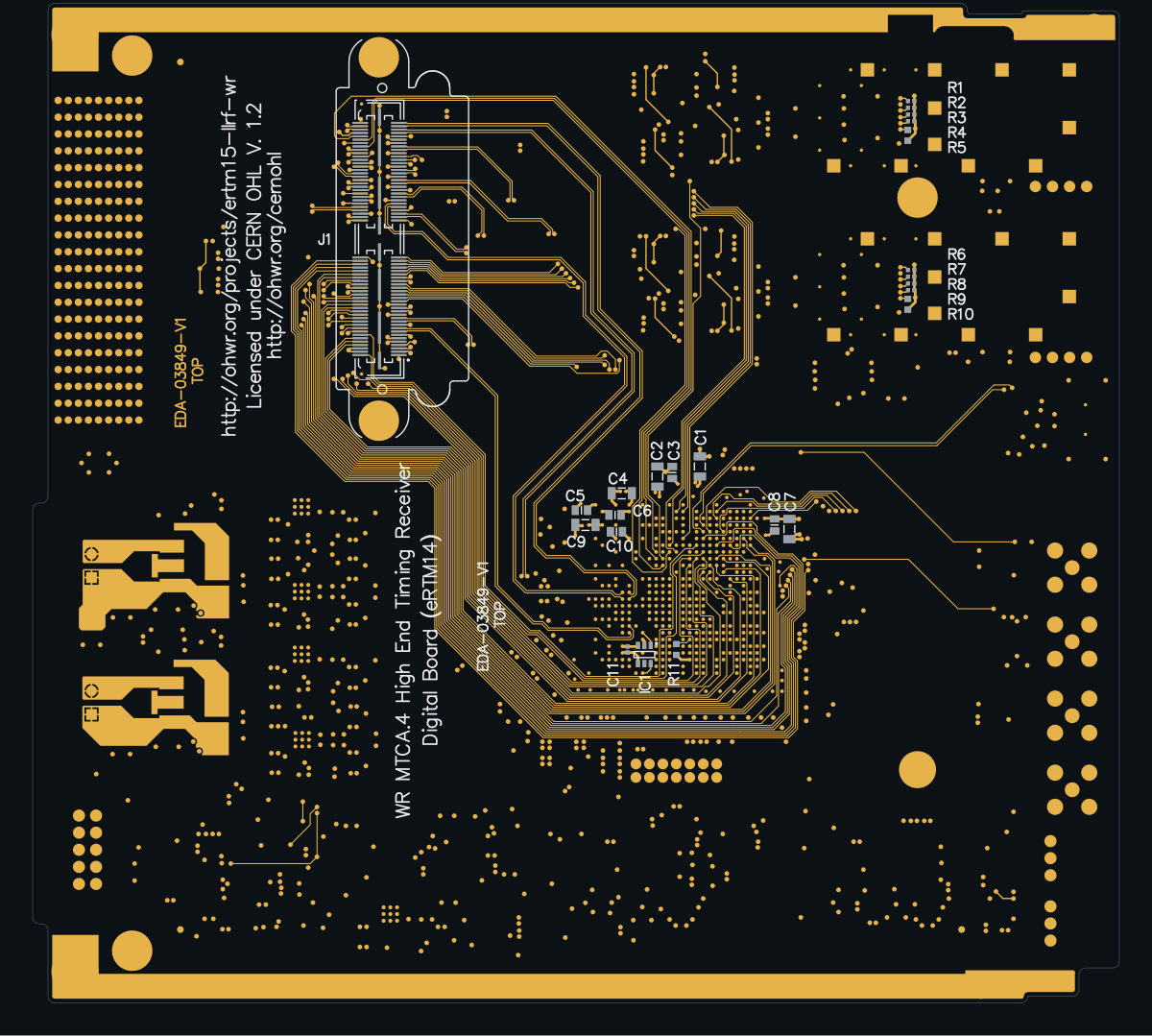
ERTM15 LLRF WR EDA 03849 (OHWR0041 R1) is an open-hardware circuit board from the CERN Open Hardware Repository, designed in Altium Designer: a 10-layer board of 161.5 × 148.5 mm with 530 components and 440 nets, published under CERN-OHL-1.2.
review 83% walked · 13 findings: 2 blocker · 6 major · 5 minor (27 items)
Open in the interactive viewerRead the full review
Design review
Probe recorded 13 findings: 2 blocker · 6 major · 5 minor (27 items) on this design. Each is shown here with its reasoning; the full review links every one to the pins, nets and datasheet pages it rests on.
A P12V via land on inner layer L8 overlaps the TEMP_SDA track at (87.68, 118.26): 12 V shorted to the temperature-sensor I2C data line in the exported copper
On inner layer L8 at (87.68, 118.26) mm, the land of a P12V via sits across the TEMP_SDA track, so the 12 V input is shorted to the temperature-sensor I2C data line in the copper as exported.
What the copper shows
The piece image of the site (L8, 85.2-90.2 x 115.8-120.8 mm) shows the TEMP_SDA track running straight through the round P12V via land, with no clearance between them.
Why it matters
If the fabricated board matches this export, 12 V reaches every device on TEMP_SDA at power-up and damages them. One possibility is that the via's L8 land is a non-functional pad that the CAM step would remove. Please check the fabrication data for that via, or move the track or the via.
- CopperShortBetweenNetsblockerOpen
P12V and TEMP_SDA copper touch on L8, at (87.68, 118.26): the two nets are shorted in the copper as exported
P12V and TEMP_SDA copper touch on L8, at (87.68, 118.26): the two nets are shorted in the copper as exported. Where: L8 at (87.68, 118.26) (one net's copper edge lies in the other's copper). The netlist still puts the two nets apart, so every connectivity check passes; the copper the fab builds joins them. The usual cause is a pour filled before the other net's via or pad was placed (or moved), so it runs through it without a clearance: refill the zones, check the CAD tool's DRC is clean, and export again. copper-near at a site shows both nets' copper at distance 0.
At short:P12V|TEMP_SDA
- PartLifecyclemajorOpen
973028 on 2 placements (RJ30, RJ31): the distributor catalogue reports "Obsolete" for TE Connectivity Erni's 973028
973028 on 2 placements (RJ30, RJ31): the distributor catalogue reports "Obsolete" for TE Connectivity Erni's 973028 — a sourcing/longevity risk to confirm against the MANUFACTURER before acting. This board's BOM names ERNI, and that is one line with TE Connectivity Erni: Tyco Electronics renamed itself TE Connectivity in March 2011, and TE completed its acquisition of ERNI Group AG (ERNI Electronics) in September 2021. A distributor delisting is not the same claim as the part being unavailable; check the vendor's own lifecycle/product-change notice for the status and any named successor. Re-read the source: GET /api/odb/parts/973028/providers (which provider said it, the maker and part number it matched, its own words, and when we asked). THE LAST BUY DATE HAS PASSED (2022-11-30, 1,446 day(s) ago), so this is a substitution rather than a buy. The distributor reports NONE left. No approved alternate is recorded for this position.
At RJ30
- DecapViaFanoutmajorOpen
C144 on 'P1V0_GTX': its rail pad reaches its via over 3.43 mm of track, adding about 1.29 nH to its loop, past Probe's 0.5 nH starting value; put the vias at the pads
C144 on 'P1V0_GTX': its rail pad reaches its via over 3.43 mm of track, adding about 1.29 nH to its loop, past Probe's 0.5 nH starting value; put the vias at the pads. C144.2 (rail) runs 3.43 mm along its copper to its nearest via, 2.43 mm past the 1 mm beside the pad: 1.29 nH; C144.1 (ground) not measured: the pad sits in a pour of its net on its own layer, which has no track length to measure. Each run past the pad as one conductor of a pair 1.80 mm apart (the pad pitch), 0.2 l ln(D/R) nH with R 0.127 mm (the track's width is not read): 1.29 nH in all. Put the vias at the pads (or in them), one per pad at least, the rail's and the ground's close together; the capacitor's own inductance as mounted is 1.42 nH (pad 0.10 nH + no via of the first net within 1 mm of its pad: the study's 0.6 nH per mm of 1.35 mm depth, ASSUMED). 0.5 nH is Probe's starting value, about the whole mounted inductance of a well-mounted 0402.
At C144
- DecapOrdermajorOpen
DecapOrder: 3 findings (2 components, 1 pin)×3
3 checked by the review by Claude walker W4 (Cern session) — 3 different reasons
At IC12, IC18, IC22.51
Each finding, with its own headline
IC12IC12 supply pins 39, 40 on 'P12V': the smallest capacitor C109 sits 3.9 mm away, behind C103 at 2.5 mm
IC12 supply pins 39, 40 on 'P12V': the smallest capacitor C109 sits 3.9 mm away, behind C103 at 2.5 mm. IC12.39: the smallest value, C109 (100 nF), is 3.9 mm from the pin and C103 (47 uF) 2.5 mm: the high-frequency part sits behind more inductance than the bulk part, which needs it least. IC12.40: the smallest value, C109 (100 nF), is 3.1 mm from the pin and C103 (47 uF) 2.0 mm: the high-frequency part sits behind more inductance than the bulk part, which needs it least. Swap them, or bring the smallest value to the pin: it serves the fastest current and is the one the loop inductance defeats. Distances are pad centre to pin centre in the board plane. The 5 mm radius, the 10x value step and the 1 mm / 1.5x tie tolerance are Probe's starting values.
IC18IC18 supply pins 39, 40 on 'P12V': the smallest capacitor C164 sits 3.9 mm away, behind C151 at 2.5 mm
IC18 supply pins 39, 40 on 'P12V': the smallest capacitor C164 sits 3.9 mm away, behind C151 at 2.5 mm. IC18.39: the smallest value, C164 (100 nF), is 3.9 mm from the pin and C151 (47 uF) 2.5 mm: the high-frequency part sits behind more inductance than the bulk part, which needs it least. IC18.40: the smallest value, C164 (100 nF), is 3.1 mm from the pin and C151 (47 uF) 2.0 mm: the high-frequency part sits behind more inductance than the bulk part, which needs it least. Swap them, or bring the smallest value to the pin: it serves the fastest current and is the one the loop inductance defeats. Distances are pad centre to pin centre in the board plane. The 5 mm radius, the 10x value step and the 1 mm / 1.5x tie tolerance are Probe's starting values.
IC22.51IC22 supply pin 51 on 'P3V3_PLL_B': the smallest capacitor C238 sits 3.3 mm away, behind C230 at 1.9 mm
IC22 supply pin 51 on 'P3V3_PLL_B': the smallest capacitor C238 sits 3.3 mm away, behind C230 at 1.9 mm. IC22.51: the smallest value, C238 (100 nF), is 3.3 mm from the pin and C230 (4.7 uF) 1.9 mm: the high-frequency part sits behind more inductance than the bulk part, which needs it least. Swap them, or bring the smallest value to the pin: it serves the fastest current and is the one the loop inductance defeats. Distances are pad centre to pin centre in the board plane. The 5 mm radius, the 10x value step and the 1 mm / 1.5x tie tolerance are Probe's starting values.
- EsdProtectorPlacementmajorOpen
EsdProtectorPlacement: 4 components×4
4 checked by the review by Claude walker W4 (Cern session) — 2 different reasons
At IC13, IC9
Each finding, with its own headline
IC13IC13.2 on 'NetIC13_2': IC13.2 hangs 11.38 mm off the line (limit 1 mm, default
IC13 (PRTR5V0U2X) protects 'NetIC13_2' at J6.1. Along the copper: 22.6 mm of track from the contact, 0 via(s) before it, on a 11.38 mm branch off the line; the line runs 11.21 mm on to R83.2; IC13 sits 10.58 mm farther from the contact than the nearest place outside J6.
IC13.2 hangs 11.38 mm off the line (limit 1 mm, default: no datasheet figure on file): the line carries the strike past it while the clamp is reached through the branch. IC13 joins the line 11.22 mm from J6.1 on a 11.21 mm run to R83.2: nearer the far end than the contact, so the surge travels most of the line before it is clamped.
Measured on the copper the ODB states: tracks, the pads they land on, and the netlist's vias. Not a straight line between centroids.
IC13IC13.3 on 'NetIC13_3': IC13.3 hangs 4.89 mm off the line (limit 1 mm, default
IC13 (PRTR5V0U2X) protects 'NetIC13_3' at R81.2, where a strike from J5.1 through R81 enters the net. Along the copper: 6.56 mm of track from the contact, 0 via(s) before it, on a 4.89 mm branch off the line; the line runs 1.67 mm on to T6.1; IC13 sits 2.95 mm farther from the contact than the nearest place outside R81.
No protection network is recognised at the entry: R81 (6R8) is in series at the entry, but 6.8 ohm is below the 100 ohm that limits a strike, so it is not counted as a protection network.
IC13.3 hangs 4.89 mm off the line (limit 1 mm, default: no datasheet figure on file): the line carries the strike past it while the clamp is reached through the branch.
Measured on the copper the ODB states: tracks, the pads they land on, and the netlist's vias. Not a straight line between centroids.
IC9IC9.2 on 'NetIC8_5': 2 via(s) between J4.2 and IC9.2
IC9 (PRTR5V0U2X) protects 'NetIC8_5' at J4.2. Along the copper: 5.96 mm of track from the contact, 2 via(s) before it, the line runs through its pad (flow-through); the line runs 8.32 mm on to IC8.5; IC9 sits 1.65 mm farther from the contact than the nearest place outside J4.
2 via(s) between J4.2 and IC9.2: the strike reaches an inner layer before it is clamped. IC9 joins the line 5.96 mm from J4.2 on a 8.32 mm run to IC8.5: nearer the far end than the contact, so the surge travels most of the line before it is clamped.
Measured on the copper the ODB states: tracks, the pads they land on, and the netlist's vias. Not a straight line between centroids.
IC9IC9.3 on 'NetIC8_4': IC9 joins the line 5.91 mm from J4.3 on a 8.03 mm run to IC8.4
IC9 (PRTR5V0U2X) protects 'NetIC8_4' at J4.3. Along the copper: 5.91 mm of track from the contact, 0 via(s) before it, the line runs through its pad (flow-through); the line runs 8.03 mm on to IC8.4; IC9 sits 1.65 mm farther from the contact than the nearest place outside J4.
IC9 joins the line 5.91 mm from J4.3 on a 8.03 mm run to IC8.4: nearer the far end than the contact, so the surge travels most of the line before it is clamped.
Measured on the copper the ODB states: tracks, the pads they land on, and the netlist's vias. Not a straight line between centroids.
- PartLifecyclemajorOpen
PartLifecycle: 3 part numbers×3
2 Obsolete, 1 Not For New Designs · on 4 placements
At IC1, IC27, IC8
Each finding, with its own headline
IC1TMP100NA/250 on 2 placements (IC1, IC16): the distributor catalogue reports "Obsolete" for Texas Instruments's TMP100NA/250
TMP100NA/250 on 2 placements (IC1, IC16): the distributor catalogue reports "Obsolete" for Texas Instruments's TMP100NA/250 — a sourcing/longevity risk to confirm against the MANUFACTURER before acting. That is the maker this board's BOM names (TEXAS INSTRUMENTS). A distributor delisting is not the same claim as the part being unavailable; check the vendor's own lifecycle/product-change notice for the status and any named successor. Re-read the source: GET /api/odb/parts/TMP100NA/250/providers (which provider said it, the maker and part number it matched, its own words, and when we asked). THE LAST BUY DATE HAS PASSED (2024-02-09, 1,010 day(s) ago), so this is a substitution rather than a buy. The distributor reports NONE left. No approved alternate is recorded for this position.
IC27LTC6957IDD-2#PBF on IC27: the distributor catalogue reports "Obsolete" for Analog Devices Inc.'s LTC6957IDD-2#PBF
LTC6957IDD-2#PBF on IC27: the distributor catalogue reports "Obsolete" for Analog Devices Inc.'s LTC6957IDD-2#PBF — a sourcing/longevity risk to confirm against the MANUFACTURER before acting. This board's BOM names LINEAR TECHNOLOGY, and that is one line with Analog Devices Inc.: Analog Devices completed its acquisitions of Hittite Microwave on 2014-07-22, Linear Technology on 2017-03-10 and Maxim Integrated on 2021-08-26. A distributor delisting is not the same claim as the part being unavailable; check the vendor's own lifecycle/product-change notice for the status and any named successor. Re-read the source: GET /api/odb/parts/LTC6957IDD-2#PBF/providers (which provider said it, the maker and part number it matched, its own words, and when we asked). THE LAST BUY DATE HAS PASSED (2025-01-17, 667 day(s) ago), so this is a substitution rather than a buy. The distributor reports NONE left. No approved alternate is recorded for this position.
IC8CP2102-GM on IC8: the distributor catalogue reports "Not For New Designs" for Silicon Labs's CP2102-GM
CP2102-GM on IC8: the distributor catalogue reports "Not For New Designs" for Silicon Labs's CP2102-GM — a sourcing/longevity risk to confirm against the MANUFACTURER before acting. That is the maker this board's BOM names (SILICON LABS). A distributor delisting is not the same claim as the part being unavailable; check the vendor's own lifecycle/product-change notice for the status and any named successor. Re-read the source: GET /api/odb/parts/CP2102-GM/providers (which provider said it, the maker and part number it matched, its own words, and when we asked). No approved alternate is recorded for this position.
- SinglePointNetmajorOpen
SinglePointNet: 6 pins×6
6 checked by the review by Claude walker (cern session) — 6 different reasons
At IC11.10, IC11.8, IC17.10, IC17.8, IC28.10, IC28.8
Each finding, with its own headline
IC11.10IC11.10 (FB2) is an IC input left unconnected
Pin IC11.10 (FB2) is an IC INPUT left UNCONNECTED (on the no-connect bucket). Marked no-connect by the designer, but an input normally needs a defined level - confirm it is truly meant to float. If the datasheet defines this input left open (an internal pull, "read as low when left floating", or a tri-level input whose open state is one of its settings), file it on the pin as if_unused (pull_up, pull_down or may_float) with submit_pin_behavior, citing the page, and this finding clears.
IC11.8IC11.8 (SS_CTRL2) is an IC input left unconnected
Pin IC11.8 (SS_CTRL2) is an IC INPUT left UNCONNECTED (on the no-connect bucket). Marked no-connect by the designer, but an input normally needs a defined level - confirm it is truly meant to float. If the datasheet defines this input left open (an internal pull, "read as low when left floating", or a tri-level input whose open state is one of its settings), file it on the pin as if_unused (pull_up, pull_down or may_float) with submit_pin_behavior, citing the page, and this finding clears.
IC17.10IC17.10 (FB2) is an IC input left unconnected
Pin IC17.10 (FB2) is an IC INPUT left UNCONNECTED (on the no-connect bucket). Marked no-connect by the designer, but an input normally needs a defined level - confirm it is truly meant to float. If the datasheet defines this input left open (an internal pull, "read as low when left floating", or a tri-level input whose open state is one of its settings), file it on the pin as if_unused (pull_up, pull_down or may_float) with submit_pin_behavior, citing the page, and this finding clears.
IC17.8IC17.8 (SS_CTRL2) is an IC input left unconnected
Pin IC17.8 (SS_CTRL2) is an IC INPUT left UNCONNECTED (on the no-connect bucket). Marked no-connect by the designer, but an input normally needs a defined level - confirm it is truly meant to float. If the datasheet defines this input left open (an internal pull, "read as low when left floating", or a tri-level input whose open state is one of its settings), file it on the pin as if_unused (pull_up, pull_down or may_float) with submit_pin_behavior, citing the page, and this finding clears.
IC28.10IC28.10 (FB2) is an IC input left unconnected
Pin IC28.10 (FB2) is an IC INPUT left UNCONNECTED (on the no-connect bucket). Marked no-connect by the designer, but an input normally needs a defined level - confirm it is truly meant to float. If the datasheet defines this input left open (an internal pull, "read as low when left floating", or a tri-level input whose open state is one of its settings), file it on the pin as if_unused (pull_up, pull_down or may_float) with submit_pin_behavior, citing the page, and this finding clears.
IC28.8IC28.8 (SS_CTRL2) is an IC input left unconnected
Pin IC28.8 (SS_CTRL2) is an IC INPUT left UNCONNECTED (on the no-connect bucket). Marked no-connect by the designer, but an input normally needs a defined level - confirm it is truly meant to float. If the datasheet defines this input left open (an internal pull, "read as low when left floating", or a tri-level input whose open state is one of its settings), file it on the pin as if_unused (pull_up, pull_down or may_float) with submit_pin_behavior, citing the page, and this finding clears.
FPGA IC10 PUDC_B (ball B25) is left floating: its only connection is the DIN input of DAC IC20
Conclusion
Ball B25 of the Kintex-7 FPGA IC10 (XC7K70T-2FBG676C) is the multi-function pin IO_L3P_T0_DQS_PUDC_B_14. It is wired only to pin 7 (DIN) of the main DAC IC20 (AD5662), net MAIN_DAC.DIN. Nothing else is on the net: no pull-up to VCCO_14 (P3V3) and no pull-down to GND. The DAC's DIN is a CMOS input, so nothing drives the net before or during configuration and PUDC_B floats.
UG475 (Table 1-12, p.22) says PUDC_B must be tied, directly or through 1 kOhm or less, to VCCO_14 or GND, and warns: "Do not allow this pin to float before and during configuration." PUDC_B decides whether the internal pull-ups on every SelectIO pin are enabled from power-up until configuration finishes. With it floating, the pre-configuration state of all user I/O on the board is undefined and may vary from one power-up to the next. That affects the DAC control lines, the PLL resets and chip selects, the SFP TX_DISABLE lines and the mezzanine control lines on J1, all of which are driven only by IC10.
Limit vs actual
Item Datasheet requirement Board Margin PUDC_B (B25) termination tied directly or via <= 1 kOhm to VCCO_14 or GND (UG475 p.22) no resistor; net = IC10.B25 + IC20.7 only requirement not met Pin state before and during configuration must not float (UG475 p.22) floats (IC20 DIN is an input) not met Connectivity
``
mermaid graph LR B25["IC10 ball B25<br/>IO_L3P_T0_DQS_PUDC_B_14<br/>(bank 14, VCCO = P3V3)"] -- MAIN_DAC.DIN --> DIN["IC20 AD5662 pin 7 DIN<br/>(CMOS input)"] B25 -. "no pull-up to P3V3<br/>no pull-down to GND" .- X["(nothing)"]``Suggested fix
Move MAIN_DAC.DIN to a free bank-14 ball (bank 14 has spare I/O) and strap B25 to GND or to P3V3 through 1 kOhm or less, choosing the polarity for the pre-configuration pull-up behaviour the design wants. Alternatively, keep the sharing and add a strap of 1 kOhm or less on MAIN_DAC.DIN. The gateware then has to drive DIN against that strap after configuration, which the AD5662 input allows but which costs static current.
PPS-in ESD clamp IC13 is routed after the MOSFET gate T6 it protects (J5 to R81 to T6 gate, then IC13)
Conclusion
On the PPS input, the SMA J5 feeds R81 (6R8) into node NetIC13_3. That node carries the gate of the N-MOSFET T6 (BSH103, pin 1), the 43 R termination R80 to GND, and the protected I/O of the ESD diode array IC13 (PRTR5V0U2X, pin 3). On the bottom copper the trace from R81 pad 2 runs to the T6 gate pad first and only then continues to IC13 pin 3. T6 is therefore electrically and physically nearer the connector than its clamp. During an ESD strike the discharge current passes the gate on its way to the clamp, so the gate sees the clamp voltage plus the inductive drop of the T6-to-IC13 trace. The BSH103 gate is rated only ±8 V DC (BSH103 datasheet p.3), while IC13 is rated for IEC 61000-4-2 8 kV and is meant to be the first thing the surge meets.
Limit vs actual (bottom side, board coordinates, mm)
Item Expected Board Margin Order along the path from J5 connector, clamp, protected device J5 (x 228.6), R81 (222.7), T6 gate pad (221.85), IC13 pin 3 (218.15) clamp is about 3.7 mm beyond the gate T6 VGS rating ±8 V DC (BSH103 p.3) protected only by IC13 downstream of it, with 6.8 Ohm series depends on trace inductance, not guaranteed Path
``
mermaid graph LR J5["J5 SMA PPS in"] --> R81["R81 6R8"] --> G["T6 BSH103 gate (pin 1)"] --> C["IC13 PRTR5V0U2X pin 3"] --> R80["R80 43R to GND"]``Suggested fix
Route R81 into IC13 pin 3 first and branch to the T6 gate from the clamp pad, or swap T6 and IC13. Optionally add a small series resistor between the node and the T6 gate so the gate is not directly on the surge path.
- DecapViaFanoutminorOpen
DecapViaFanout: 2 components×2
2 checked by the review by Claude walker W4 (Cern session) — 2 different reasons
At C123, C170
Each finding, with its own headline
C123C123 on 'P1V0': its rail pad reaches its via over 1.82 mm of track, adding about 0.64 nH to its loop, past Probe's 0.5 nH starting value; put the vias at the pads (a 330 uF bulk capacitor: its inductance matters only far above the band it serves)
C123 on 'P1V0': its rail pad reaches its via over 1.82 mm of track, adding about 0.64 nH to its loop, past Probe's 0.5 nH starting value; put the vias at the pads (a 330 uF bulk capacitor: its inductance matters only far above the band it serves). C123.1 (rail) runs 1.82 mm along its copper to its nearest via, 0.82 mm past the 1 mm beside the pad: 0.64 nH; C123.2 (ground) not measured: the pad sits in a pour of its net on its own layer, which has no track length to measure. Each run past the pad as one conductor of a pair 6.20 mm apart (the pad pitch), 0.2 l ln(D/R) nH with R 0.127 mm (the track's width is not read): 0.64 nH in all. Put the vias at the pads (or in them), one per pad at least, the rail's and the ground's close together; the capacitor's own inductance as mounted is 2.01 nH (pad 0.20 nH + no via of the first net within 1 mm of its pad: the study's 0.6 nH per mm of 1.35 mm depth, ASSUMED). 0.5 nH is Probe's starting value, about the whole mounted inductance of a well-mounted 0402.
C170C170 on 'NetC170_2': its rail pad reaches its via over 2.70 mm of track, adding about 0.90 nH to its loop, past Probe's 0.5 nH starting value; put the vias at the pads (a 4.7 uF bulk capacitor: its inductance matters only far above the band it serves)
C170 on 'NetC170_2': its rail pad reaches its via over 2.70 mm of track, adding about 0.90 nH to its loop, past Probe's 0.5 nH starting value; put the vias at the pads (a 4.7 uF bulk capacitor: its inductance matters only far above the band it serves). C170.2 (rail) runs 2.70 mm along its copper to its nearest via, 1.70 mm past the 1 mm beside the pad: 0.90 nH; C170.1 (ground) not measured: the pad sits in a pour of its net on its own layer, which has no track length to measure. Each run past the pad as one conductor of a pair 1.80 mm apart (the pad pitch), 0.2 l ln(D/R) nH with R 0.127 mm (the track's width is not read): 0.90 nH in all. Put the vias at the pads (or in them), one per pad at least, the rail's and the ground's close together; the capacitor's own inductance as mounted is 1.03 nH (pad 0.10 nH + no via of the first net within 1 mm of its pad: the study's 0.6 nH per mm of 0.70 mm depth, ASSUMED). 0.5 nH is Probe's starting value, about the whole mounted inductance of a well-mounted 0402.
- ReferencePlaneDiscontinuityminorOpen
ReferencePlaneDiscontinuity: 2 boards×2
2 checked by the review by Claude walker W4 (Cern session) — 2 different reasons
At refchange:GND|P1V0, refchange:GND|P2V5
Each finding, with its own headline
refchange:GND|P1V010 nets change reference between GND and P1V0 at 14 vias, each with another reference that continues across (fastest: CONFIG_DONE at 100 ps 10-90 %, ASSUMED)
At 14 via(s), on 10 net(s), the signal leaves a layer referenced by one of GND and P1V0 for a layer referenced by the other, and no plane references both layers. Different nets: no via can carry the return across; only decoupling between the two planes near the via can. The capacitor carrying the return across was measured at each via, at the knee of the crossing net's edge against 50 ohm assumed: 14 with none. 14 of them at an ASSUMED edge (no edge on file for the net): state one (net_timing_state) and it is re-read. One decision covers the pair: whether GND and P1V0 are decoupled to each other near these vias. A via whose layers have more references than these two is a site of each pair it joins. Every one is partial: another reference continues across through a stitching via of its net, so only part of the return has nowhere to go, and the finding is the lower tier (info). They are listed with the farthest stitching via first.
- 'TEMP_SCL' at (137.25, 126.45), L3 -> L8: GND on L2_GND, P1V0 on L4_PWR to GND on L7_GND, GND on L9_GND; partial, GND continues through a via of GND 8.47 mm away; stitching none, 119.8 mm of track past the via on L8: At the 5 GHz knee of a 100 ps edge (10 ns 10-90 %, assumed: no edge is on file for the net) no capacitor carries the return; only the planes do. GND and P1V0 are not a thin pair (at most 0.2 mm), so their own capacitance does not carry the return. To serve it, change layers across the same plane, or move the signal to a layer referenced to ground. None.
- 'TEMP_SDA' at (138, 127.1), L3 -> L8: GND on L2_GND, P1V0 on L4_PWR to GND on L7_GND, GND on L9_GND; partial, GND continues through a via of GND 7.57 mm away; stitching none, 119.5 mm of track past the via on L8: At the 5 GHz knee of a 100 ps edge (10 ns 10-90 %, assumed: no edge is on file for the net) no capacitor carries the return; only the planes do. GND and P1V0 are not a thin pair (at most 0.2 mm), so their own capacitance does not carry the return. To serve it, change layers across the same plane, or move the signal to a layer referenced to ground. None.
- 'CONFIG_DONE' at (158.9, 113.4), L3 -> BOTTOM_LAYER: GND on L2_GND, P1V0 on L4_PWR to GND on L9_GND; partial, GND continues through a via of GND 3.33 mm away; stitching none, 55.9 mm of track past the via on BOTTOM_LAYER: At the 5 GHz knee of a 100 ps edge (100 ps 10-90 %, assumed: no edge is on file for the net) no capacitor carries the return; only the planes do. GND and P1V0 are not a thin pair (at most 0.2 mm), so their own capacitance does not carry the return. To serve it, change layers across the same plane, or move the signal to a layer referenced to ground. None.
- 'CONFIG_DONE' at (174.8, 133), L3 -> BOTTOM_LAYER: GND on L2_GND, P1V0 on L4_PWR to GND on L9_GND; partial, GND continues through a via of GND 1 mm away; stitching none, 55.9 mm of track past the via on BOTTOM_LAYER: At the 5 GHz knee of a 100 ps edge (100 ps 10-90 %, assumed: no edge is on file for the net) no capacitor carries the return; only the planes do. GND and P1V0 are not a thin pair (at most 0.2 mm), so their own capacitance does not carry the return. To serve it, change layers across the same plane, or move the signal to a layer referenced to ground. None.
- '\R\E\S\E\T\_1' at (158.9, 111.4), L3 -> BOTTOM_LAYER: GND on L2_GND, P1V0 on L4_PWR to GND on L9_GND; partial, GND continues through a via of GND 4.44 mm away; stitching none, 52.7 mm of track past the via on BOTTOM_LAYER: At the 5 GHz knee of a 100 ps edge (100 ps 10-90 %, assumed: no edge is on file for the net) no capacitor carries the return; only the planes do. GND and P1V0 are not a thin pair (at most 0.2 mm), so their own capacitance does not carry the return. To serve it, change layers across the same plane, or move the signal to a layer referenced to ground. None.
- '\R\E\S\E\T\_1' at (168.8, 131), L3 -> BOTTOM_LAYER: GND on L2_GND, P1V0 on L4_PWR to GND on L9_GND; partial, GND continues through a via of GND 1 mm away; stitching none, 52.7 mm of track past the via on BOTTOM_LAYER: At the 5 GHz knee of a 100 ps edge (100 ps 10-90 %, assumed: no edge is on file for the net) no capacitor carries the return; only the planes do. GND and P1V0 are not a thin pair (at most 0.2 mm), so their own capacitance does not carry the return. To serve it, change layers across the same plane, or move the signal to a layer referenced to ground. None.
- 'NetIC10_C8' at (158.9, 114.5), L3 -> BOTTOM_LAYER: GND on L2_GND, P1V0 on L4_PWR to GND on L9_GND; partial, GND continues through a via of GND 2.73 mm away; stitching none, 49.4 mm of track past the via on BOTTOM_LAYER: At the 5 GHz knee of a 100 ps edge (100 ps 10-90 %, assumed: no edge is on file for the net) no capacitor carries the return; only the planes do. GND and P1V0 are not a thin pair (at most 0.2 mm), so their own capacitance does not carry the return. To serve it, change layers across the same plane, or move the signal to a layer referenced to ground. None.
- 'NetIC10_C8' at (180.8, 133), L3 -> BOTTOM_LAYER: GND on L2_GND, P1V0 on L4_PWR to GND on L9_GND; partial, GND continues through a via of GND 1 mm away; stitching none, 49.4 mm of track past the via on BOTTOM_LAYER: At the 5 GHz knee of a 100 ps edge (100 ps 10-90 %, assumed: no edge is on file for the net) no capacitor carries the return; only the planes do. GND and P1V0 are not a thin pair (at most 0.2 mm), so their own capacitance does not carry the return. To serve it, change layers across the same plane, or move the signal to a layer referenced to ground. None.
- 'CRC_ERROR' at (158.9, 112.5), L3 -> BOTTOM_LAYER: GND on L2_GND, P1V0 on L4_PWR to GND on L9_GND; partial, GND continues through a via of GND 3.98 mm away; stitching none, 47.5 mm of track past the via on BOTTOM_LAYER: At the 5 GHz knee of a 100 ps edge (100 ps 10-90 %, assumed: no edge is on file for the net) no capacitor carries the return; only the planes do. GND and P1V0 are not a thin pair (at most 0.2 mm), so their own capacitance does not carry the return. To serve it, change layers across the same plane, or move the signal to a layer referenced to ground. None.
- 'CRC_ERROR' at (175.8, 132), L3 -> BOTTOM_LAYER: GND on L2_GND, P1V0 on L4_PWR to GND on L9_GND; partial, GND continues through a via of GND 1 mm away; stitching none, 47.5 mm of track past the via on BOTTOM_LAYER: At the 5 GHz knee of a 100 ps edge (100 ps 10-90 %, assumed: no edge is on file for the net) no capacitor carries the return; only the planes do. GND and P1V0 are not a thin pair (at most 0.2 mm), so their own capacitance does not carry the return. To serve it, change layers across the same plane, or move the signal to a layer referenced to ground. None.
- 'FPGA_TCK_9' at (172.8, 133), L3 -> BOTTOM_LAYER: GND on L2_GND, P1V0 on L4_PWR to GND on L9_GND; partial, GND continues through a via of GND 1.41 mm away; stitching none, 0.7 mm of track past the via on BOTTOM_LAYER: At the 5 GHz knee of a 100 ps edge (2 ns 10-90 %, assumed: no edge is on file for the net) no capacitor carries the return; only the planes do. GND and P1V0 are not a thin pair (at most 0.2 mm), so their own capacitance does not carry the return. To serve it, change layers across the same plane, or move the signal to a layer referenced to ground. None.
- 'FPGA_TDI_9' at (167.8, 131), L3 -> BOTTOM_LAYER: GND on L2_GND, P1V0 on L4_PWR to GND on L9_GND; partial, GND continues through a via of GND 1 mm away; stitching none, 0.7 mm of track past the via on BOTTOM_LAYER: At the 5 GHz knee of a 100 ps edge (2 ns 10-90 %, assumed: no edge is on file for the net) no capacitor carries the return; only the planes do. GND and P1V0 are not a thin pair (at most 0.2 mm), so their own capacitance does not carry the return. To serve it, change layers across the same plane, or move the signal to a layer referenced to ground. None.
- and 2 more
Every site is a row of this finding's evidence, keyed by net, layers and position. GET /api/odb/boards/42/reference-planes?group=refchange%3AGND%7CP1V0 serves each with its own layer_image region; all of them lie in x 135.25..182.8, y 109.4..135 mm (board frame, Y up).
The reference on each layer is the first plane the track meets leaving the via, anti-pads and the net's own copper skipped. Whether it matters depends on each signal's edge rate, which nothing on file states for these nets: a slow static line crosses a split harmlessly, a fast edge does not.
refchange:GND|P2V540 nets change reference between GND and P2V5 at 70 vias, each with another reference that continues across (fastest: EXT_PLL_CTRL.PLL_CS_1 at 100 ps 10-90 %, ASSUMED)
At 70 via(s), on 40 net(s), the signal leaves a layer referenced by one of GND and P2V5 for a layer referenced by the other, and no plane references both layers. Different nets: no via can carry the return across; only decoupling between the two planes near the via can. The capacitor carrying the return across was measured at each via, at the knee of the crossing net's edge against 50 ohm assumed: 70 with none. 70 of them at an ASSUMED edge (no edge on file for the net): state one (net_timing_state) and it is re-read. One decision covers the pair: whether GND and P2V5 are decoupled to each other near these vias. A via whose layers have more references than these two is a site of each pair it joins. Every one is partial: another reference continues across through a stitching via of its net, so only part of the return has nowhere to go, and the finding is the lower tier (info). They are listed with the farthest stitching via first.
- 'MAIN_DAC.DIN' at (193.1, 121.35), L3 -> BOTTOM_LAYER: GND on L2_GND, P2V5 on L4_PWR to GND on L9_GND; partial, GND continues through a via of GND 4.03 mm away; stitching none, 71.4 mm of track past the via on BOTTOM_LAYER: At the 5 GHz knee of a 100 ps edge (100 ps 10-90 %, assumed: no edge is on file for the net) no capacitor carries the return; only the planes do. GND and P2V5 are not a thin pair (at most 0.2 mm), so their own capacitance does not carry the return. To serve it, change layers across the same plane, or move the signal to a layer referenced to ground. None.
- 'MAIN_DAC.DIN' at (192.4, 119.8), L3 -> BOTTOM_LAYER: GND on L2_GND, P2V5 on L4_PWR to GND on L9_GND; partial, GND continues through a via of GND 3.42 mm away; stitching none, 71.4 mm of track past the via on BOTTOM_LAYER: At the 5 GHz knee of a 100 ps edge (100 ps 10-90 %, assumed: no edge is on file for the net) no capacitor carries the return; only the planes do. GND and P2V5 are not a thin pair (at most 0.2 mm), so their own capacitance does not carry the return. To serve it, change layers across the same plane, or move the signal to a layer referenced to ground. None.
- 'EXT_PLL_CTRL.PLL_RESET_1' at (197.6, 135.3), L3 -> BOTTOM_LAYER: GND on L2_GND, P2V5 on L4_PWR to GND on L9_GND; partial, GND continues through a via of GND 12.31 mm away; stitching none, 66.2 mm of track past the via on BOTTOM_LAYER: At the 5 GHz knee of a 100 ps edge (20 ns 10-90 %, assumed: no edge is on file for the net) no capacitor carries the return; only the planes do. GND and P2V5 are not a thin pair (at most 0.2 mm), so their own capacitance does not carry the return. To serve it, change layers across the same plane, or move the signal to a layer referenced to ground. None.
- 'EXT_PLL_CTRL.PLL_RESET_1' at (179.8, 149), L3 -> BOTTOM_LAYER: GND on L2_GND, P2V5 on L4_PWR to GND on L9_GND; partial, GND continues through a via of GND 1.41 mm away; stitching none, 66.2 mm of track past the via on BOTTOM_LAYER: At the 5 GHz knee of a 100 ps edge (20 ns 10-90 %, assumed: no edge is on file for the net) no capacitor carries the return; only the planes do. GND and P2V5 are not a thin pair (at most 0.2 mm), so their own capacitance does not carry the return. To serve it, change layers across the same plane, or move the signal to a layer referenced to ground. None.
- 'INT_PLL_CTRL.PLL_SDI_1' at (196, 138.7), L3 -> BOTTOM_LAYER: GND on L2_GND, P2V5 on L4_PWR to GND on L9_GND; partial, GND continues through a via of GND 12.96 mm away; stitching none, 61.6 mm of track past the via on BOTTOM_LAYER: At the 5 GHz knee of a 100 ps edge (20 ns 10-90 %, assumed: no edge is on file for the net) no capacitor carries the return; only the planes do. GND and P2V5 are not a thin pair (at most 0.2 mm), so their own capacitance does not carry the return. To serve it, change layers across the same plane, or move the signal to a layer referenced to ground. None.
- 'INT_PLL_CTRL.PLL_SDI_1' at (180.3, 153), L3 -> BOTTOM_LAYER: GND on L2_GND, P2V5 on L4_PWR to GND on L9_GND; partial, GND continues through a via of GND 2.69 mm away; stitching none, 61.6 mm of track past the via on BOTTOM_LAYER: At the 5 GHz knee of a 100 ps edge (20 ns 10-90 %, assumed: no edge is on file for the net) no capacitor carries the return; only the planes do. GND and P2V5 are not a thin pair (at most 0.2 mm), so their own capacitance does not carry the return. To serve it, change layers across the same plane, or move the signal to a layer referenced to ground. None.
- 'INT_PLL_CTRL.PLL_SDO_1' at (194.4, 139.4), L3 -> BOTTOM_LAYER: GND on L2_GND, P2V5 on L4_PWR to GND on L9_GND; partial, GND continues through a via of GND 11.3 mm away; stitching none, 59.9 mm of track past the via on BOTTOM_LAYER: At the 5 GHz knee of a 100 ps edge (20 ns 10-90 %, assumed: no edge is on file for the net) no capacitor carries the return; only the planes do. GND and P2V5 are not a thin pair (at most 0.2 mm), so their own capacitance does not carry the return. To serve it, change layers across the same plane, or move the signal to a layer referenced to ground. None.
- 'INT_PLL_CTRL.PLL_SDO_1' at (180.8, 150), L3 -> BOTTOM_LAYER: GND on L2_GND, P2V5 on L4_PWR to GND on L9_GND; partial, GND continues through a via of GND 1.41 mm away; stitching none, 59.9 mm of track past the via on BOTTOM_LAYER: At the 5 GHz knee of a 100 ps edge (20 ns 10-90 %, assumed: no edge is on file for the net) no capacitor carries the return; only the planes do. GND and P2V5 are not a thin pair (at most 0.2 mm), so their own capacitance does not carry the return. To serve it, change layers across the same plane, or move the signal to a layer referenced to ground. None.
- 'INT_PLL_CTRL.PLL_RESET_1' at (192.6, 138.1), L3 -> BOTTOM_LAYER: GND on L2_GND, P2V5 on L4_PWR to GND on L9_GND; partial, GND continues through a via of GND 9.9 mm away; stitching none, 57.8 mm of track past the via on BOTTOM_LAYER: At the 5 GHz knee of a 100 ps edge (20 ns 10-90 %, assumed: no edge is on file for the net) no capacitor carries the return; only the planes do. GND and P2V5 are not a thin pair (at most 0.2 mm), so their own capacitance does not carry the return. To serve it, change layers across the same plane, or move the signal to a layer referenced to ground. None.
- 'INT_PLL_CTRL.PLL_RESET_1' at (180.8, 148), L3 -> BOTTOM_LAYER: GND on L2_GND, P2V5 on L4_PWR to GND on L9_GND; partial, GND continues through a via of GND 1.41 mm away; stitching none, 57.8 mm of track past the via on BOTTOM_LAYER: At the 5 GHz knee of a 100 ps edge (20 ns 10-90 %, assumed: no edge is on file for the net) no capacitor carries the return; only the planes do. GND and P2V5 are not a thin pair (at most 0.2 mm), so their own capacitance does not carry the return. To serve it, change layers across the same plane, or move the signal to a layer referenced to ground. None.
- 'INT_PLL_CTRL.PLL_SCLK_1' at (189.5, 137.9), L3 -> BOTTOM_LAYER: GND on L2_GND, P2V5 on L4_PWR to GND on L9_GND; partial, GND continues through a via of GND 7.17 mm away; stitching none, 56.5 mm of track past the via on BOTTOM_LAYER: At the 5 GHz knee of a 100 ps edge (1 ns 10-90 %, assumed: no edge is on file for the net) no capacitor carries the return; only the planes do. GND and P2V5 are not a thin pair (at most 0.2 mm), so their own capacitance does not carry the return. To serve it, change layers across the same plane, or move the signal to a layer referenced to ground. None.
- 'INT_PLL_CTRL.PLL_SCLK_1' at (179.8, 147), L3 -> BOTTOM_LAYER: GND on L2_GND, P2V5 on L4_PWR to GND on L9_GND; partial, GND continues through a via of GND 1.41 mm away; stitching none, 56.5 mm of track past the via on BOTTOM_LAYER: At the 5 GHz knee of a 100 ps edge (1 ns 10-90 %, assumed: no edge is on file for the net) no capacitor carries the return; only the planes do. GND and P2V5 are not a thin pair (at most 0.2 mm), so their own capacitance does not carry the return. To serve it, change layers across the same plane, or move the signal to a layer referenced to ground. None.
- and 58 more
Every site is a row of this finding's evidence, keyed by net, layers and position. GET /api/odb/boards/42/reference-planes?group=refchange%3AGND%7CP2V5 serves each with its own layer_image region; all of them lie in x 100.4..205.1, y 90.6..213.4 mm (board frame, Y up).
The reference on each layer is the first plane the track meets leaving the via, anti-pads and the net's own copper skipped. Whether it matters depends on each signal's edge rate, which nothing on file states for these nets: a slow static line crosses a split harmlessly, a fast edge does not.
- ConnectorDomainMixedminorOpen
RJ30 takes 2 different supplies off the board on one connector: P12V (12.0 V), MP3V3 (3.3 V)
RJ30 carries 2 different supplies out of the board on one connector: P12V (12.0 V) on A10/A9/B10/B9, MP3V3 (3.3 V) on C9. Declare the intent. Two rails on one connector is ordinary in a docking or power-distribution interface and a hazard in a signal one, and the difference is not visible from the netlist — but note that adjacent contacts at different voltages are exactly what a mirrored, reversed or off-by-one cable shorts together, so the cost of getting the mating wrong is a rail collision rather than a dead signal. If this is a standard connector, declare its family (connector_family_declare) and file the standard's contact map: supplies on the contacts it assigns to power are then not reported.
At RJ30
Main parts
| Part number | Maker | Description | Where |
|---|---|---|---|
| 1734035-1 | TYCO ELECTRONICS | 5 Pin + 1 Shield USB Receptacle | J4 |
| 5PB1108PGGI | INTEGRATED DEVICE TECHNOLOGY (IDT) | 1.8V to 3.3V 1:8 LVCMOS High Performance Clock Buffer Family | IC15 |
| 70246-1004 | MOLEX | Connector 10 Male | J10 |
| 87831-1420 | MOLEX | Connector 14 Male | J8 |
| BAT15099E6327HTSA1 | INFINEON | Anti-Parallel Pair Schottky Diode | D7 |
| BSH203 | NXP SEMICONDUCTORS | P-CHANNEL MOSFET WITH DIODE | T8 |
| CDCM61002RHBT | TEXAS INSTRUMENTS | Two Output, Integrated VCO, Low-Jitter Clock Generator | IC25 |
| CP2102-GM | SILICON LABS | Single-Chip USB to UART Bridge | IC8 |
| DOT050V-010.0M | CONNOR-WINFIELD | Oscillator 4 pins 1=VCO 3=GND 4=OUT 6=VDC | OSC1 |
| FRETHE025 | PERICOM | 3.3V CMOS 25.000MHz Ethernet VCXO | OSC2 |
| FSMSM or 1437566-3 | TYCO ELECTRONICS | Push-Button Switch SPDT | PB1 |
| LTC6957IDD-2#PBF | LINEAR TECHNOLOGY | Low Phase Noise, Dual Output Buffer/Driver/Logic Converter, LVDS Logic Outputs | IC27 |
| QSH-060-01-L-D-A | SAMTEC | Connector 120 Female (2x60) + 2x4 GND | J1 |
| REF5030AID | TEXAS INSTRUMENTS | Low-Noise, Very Low Drift, Precision Voltage Reference | IC29 |
| S25FL128LAGNFV01 | CYPRESS | 128 Mbit (16 Mbyte), 3.0 V Quad SPI FL-L NOR Flash Memory | IC24 |
| STM32F303RET6 | ST MICROELECTRONICS | ARM Cortex-M4 32-bit MCU, 512 KB Flash, 80 KB Internal RAM, 52 I/Os, 64-pin LQFP, Industrial Grade | IC21 |
| TCM2-43X+ | MINI-CIRCUITS | 50 OHMS 10 to 4000 MHz RF Transformer | TR1 |
| WBC16-1TLB | COILCRAFT | SMT Transformer WBC Series Type B Pinout | TR2 |
| XC7K70T-2FBG676C | XILINX | KINTEX-7 FPGA, 300 User I/O, 8 GTXs, 676-Ball BGA, Speed Grade 2, Commercial Grade, Pb-Free | IC10 |
| 1888247-1 | TYCO ELECTRONICS | 20 Position SFP+ Connector (Small Form-factor Pluggable) | J2, J3 |
| 550-3509F | DIALIGHT | Bicolor Red/Green LED 1 Anode Red 2 Com Cathode 3 Anode Green | LD3, LD4 |
| 571-0132F | DIALIGHT | 2x LED Botom Green, Top Yellow | LD1, LD2 |
| 6367034-1 | TYCO ELECTRONICS | SFP Cage Bottom (Small Form-factor Pluggable) | CageBot1, CageBot2 |
| 6367035-1 | TYCO ELECTRONICS | SFP Cage Top (Small Form-factor Pluggable) | CageTop1, CageTop2 |
| 973028 | ERNI | 90 Contacts, 6 Rows (a,b,c,d,e,f) of 10 positions + 3 Shield Rows (ab, cd, ef) of 10 Positions, Pitch 2.5 mm, Press-Fit, Right Angle ERmet ZD High Speed Differential Hard Metric Female Connector | RJ30, RJ31 |
| AD5662BRMZ-1 | ANALOG DEVICES | 2.7V to 5.5V, 250uA, Rail-to-Rail Output 16-Bit nanoDAC | IC20, IC30 |
| AD9516-4BCPZ | ANALOG DEVICES | 14-Output Clock Generator with Integrated 1.6 GHz VCO | IC22, IC23 |
| LMZ31704RVQT | TEXAS INSTRUMENTS | 4A SIMPLE SWITCHER® Power Module with 2.95V-17V Input and Current Sharing | IC12, IC18 |
| PRTR5V0U2X | NXP SEMICONDUCTORS | Ultra Low Capacitance Double Rail-to-Rail ESD Protection Diode | IC13, IC9 |
| TMP100NA/250 | TEXAS INSTRUMENTS | Digital Temperature Sensor with I2C Interface | IC1, IC16 |
| 24AA025E48-I/SN | MICROCHIP TECHNOLOGY | 1.7V-5.5V, 2K I2C™ Serial EEPROMs with EUI-48™ Node Identity | IC26, IC6, IC7 |
| 132203 | AMPHENOL | J5, J6, J7, J9 | |
| NB6L611MNG | ON SEMICONDUCTOR | 2.5V/3.3V 1:2 Differential LVPECL Clock / Data Fanout Buffer | IC2, IC3, IC4, IC5 |
| TPS7A8901RTJT | TEXAS INSTRUMENTS | Dual, 1-A, Low-Noise (3.8-uVRMS), Low-Dropout Voltage Regulator | IC11, IC14, IC17, IC19, IC28 |
| BAS3010A-03W | INFINEON | Schottky Diode | D1, D2, D3, D4, D5, D6, D8 |
| BSH103 | NEXPERIA | N-CHANNEL MOSFET WITH DIODE | T1, T2, T3, T4, T5, T6, T7 |
| R0603_13K7_0.1%_0.063W_10PPM | GENERIC | Resistor - 0.1% | R82 |
| R0603_22K6_0.1%_0.063W_10PPM | GENERIC | Resistor - 0.1% | R79 |
| R0603_267R_0.1%_0.063W_10PPM | GENERIC | Resistor - 0.1% | R70 |
| R0603_470K_1%_0.1W_100PPM | GENERIC | Resistor - 1% | R90 |
About this design
- Design
- ERTM15 LLRF WR EDA 03849 — OHWR0041 R1
- Designed in
- Altium Designer
- Board
- 10 copper layers, 161.5 × 148.5 mm, 530 components, 440 nets
- Licence
- CERN-OHL-1.2
- Source
- https://gitlab.com/ohwr/project/ertm15-llrf-wr at commit
a7df2031cca7 - Attribution
- CERN Open Hardware Repository, project ohwr/project/ertm15-llrf-wr (commit a7df2031cca7adda4359c233106cc2161a75d4fe, 2025-04-10). Licence: CERN-OHL-1.2 (stated on the schematic sheets). Source: https://gitlab.com/ohwr/project/ertm15-llrf-wr. This is a snapshot of the copy published on the OHWR GitLab pages (R1), not CERN's released record. CERN's source of truth is EDMS (https://edms.cern.ch), and the current release may be newer.
- Reviewed with
- Probe by E# (E-Sharp AB)