 Probe

ERTM15 LLRF WR EDA 03850
OHWR0042 · revision R1
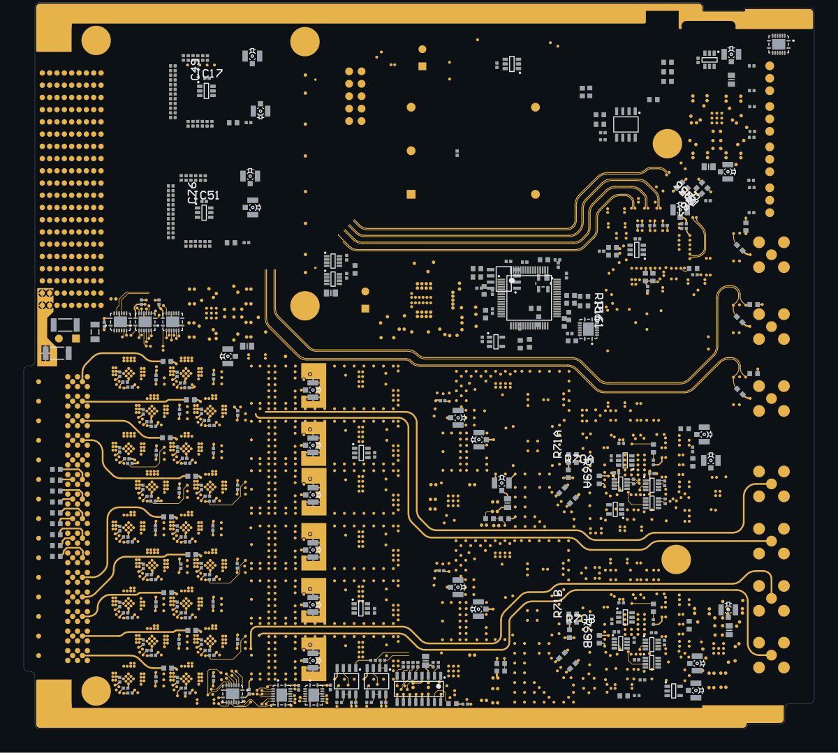
ERTM15 LLRF WR EDA 03850 (OHWR0042 R1) is an open-hardware circuit board from the CERN Open Hardware Repository, designed in Altium Designer: a 8-layer board of 161.5 × 148.5 mm with 1070 components and 729 nets, published under CERN-OHL-1.2.
review 69% walked · 17 findings: 2 blocker · 9 major · 6 minor (486 items)
Open in the interactive viewerRead the full review
Design review
Probe recorded 17 findings: 2 blocker · 9 major · 6 minor (486 items) on this design. Each is shown here with its reasoning; the full review links every one to the pins, nets and datasheet pages it rests on.
- CopperShortBetweenNetsblockerOpen
CopperShortBetweenNets: 21 boards×21
e.g. “BP_CLK_12 and GND copper touch on TOP_LAYER, at (49.75, -9.46): the two nets are shorted in the copper as exported” · 21 different statements
At short:BP_CLK_12|GND, short:BP_CLK_12|MP3V3, short:CPU_RESET_12|MP3V3, short:GND|LEDS_SCLK, short:GND|MP3V3, short:GND|NetIC6_29 and 15 more
Each finding, with its own headline
short:BP_CLK_12|GNDBP_CLK_12 and GND copper touch on TOP_LAYER, at (49.75, -9.46): the two nets are shorted in the copper as exported
BP_CLK_12 and GND copper touch on TOP_LAYER, at (49.75, -9.46): the two nets are shorted in the copper as exported. Where: TOP_LAYER at (49.75, -9.46) (one net's copper edge lies in the other's copper). The netlist still puts the two nets apart, so every connectivity check passes; the copper the fab builds joins them. The usual cause is a pour filled before the other net's via or pad was placed (or moved), so it runs through it without a clearance: refill the zones, check the CAD tool's DRC is clean, and export again. copper-near at a site shows both nets' copper at distance 0.
short:BP_CLK_12|MP3V3BP_CLK_12 and MP3V3 copper touch on TOP_LAYER, at (49.75, -8.15): the two nets are shorted in the copper as exported
BP_CLK_12 and MP3V3 copper touch on TOP_LAYER, at (49.75, -8.15): the two nets are shorted in the copper as exported. Where: TOP_LAYER at (49.75, -8.15) (one net's copper edge lies in the other's copper). The netlist still puts the two nets apart, so every connectivity check passes; the copper the fab builds joins them. The usual cause is a pour filled before the other net's via or pad was placed (or moved), so it runs through it without a clearance: refill the zones, check the CAD tool's DRC is clean, and export again. copper-near at a site shows both nets' copper at distance 0.
short:CPU_RESET_12|MP3V3CPU_RESET_12 and MP3V3 copper touch on TOP_LAYER, at (41.94, -1.11): the two nets are shorted in the copper as exported
CPU_RESET_12 and MP3V3 copper touch on TOP_LAYER, at (41.94, -1.11): the two nets are shorted in the copper as exported. Where: TOP_LAYER at (41.94, -1.11) (one net's copper edge lies in the other's copper). The netlist still puts the two nets apart, so every connectivity check passes; the copper the fab builds joins them. The usual cause is a pour filled before the other net's via or pad was placed (or moved), so it runs through it without a clearance: refill the zones, check the CAD tool's DRC is clean, and export again. copper-near at a site shows both nets' copper at distance 0.
short:GND|LEDS_SCLKGND and LEDS_SCLK copper touch on TOP_LAYER, at (53.29, -8.9): the two nets are shorted in the copper as exported
GND and LEDS_SCLK copper touch on TOP_LAYER, at (53.29, -8.9): the two nets are shorted in the copper as exported. Where: TOP_LAYER at (53.29, -8.9) (one net's copper edge lies in the other's copper). The netlist still puts the two nets apart, so every connectivity check passes; the copper the fab builds joins them. The usual cause is a pour filled before the other net's via or pad was placed (or moved), so it runs through it without a clearance: refill the zones, check the CAD tool's DRC is clean, and export again. copper-near at a site shows both nets' copper at distance 0.
short:GND|MP3V3GND and MP3V3 copper touch on TOP_LAYER, at (44.45, -1.3) and 2 other place(s): the two nets are shorted in the copper as exported
GND and MP3V3 copper touch on TOP_LAYER, at (44.45, -1.3) and 2 other place(s): the two nets are shorted in the copper as exported. Where: TOP_LAYER at (44.45, -1.3) (one net's copper edge lies in the other's copper); TOP_LAYER at (57.6, 4.47) (one net's copper edge lies in the other's copper); TOP_LAYER at (59.29, -7.05) (one net's copper edge lies in the other's copper). The netlist still puts the two nets apart, so every connectivity check passes; the copper the fab builds joins them. The usual cause is a pour filled before the other net's via or pad was placed (or moved), so it runs through it without a clearance: refill the zones, check the CAD tool's DRC is clean, and export again. copper-near at a site shows both nets' copper at distance 0.
short:GND|NetIC6_29GND and NetIC6_29 copper touch on TOP_LAYER, at (54.05, -8.88): the two nets are shorted in the copper as exported
GND and NetIC6_29 copper touch on TOP_LAYER, at (54.05, -8.88): the two nets are shorted in the copper as exported. Where: TOP_LAYER at (54.05, -8.88) (one net's copper edge lies in the other's copper). The netlist still puts the two nets apart, so every connectivity check passes; the copper the fab builds joins them. The usual cause is a pour filled before the other net's via or pad was placed (or moved), so it runs through it without a clearance: refill the zones, check the CAD tool's DRC is clean, and export again. copper-near at a site shows both nets' copper at distance 0.
short:GND|NetIC6_61GND and NetIC6_61 copper touch on TOP_LAYER, at (49.55, 2.49): the two nets are shorted in the copper as exported
GND and NetIC6_61 copper touch on TOP_LAYER, at (49.55, 2.49): the two nets are shorted in the copper as exported. Where: TOP_LAYER at (49.55, 2.49) (one net's copper edge lies in the other's copper). The netlist still puts the two nets apart, so every connectivity check passes; the copper the fab builds joins them. The usual cause is a pour filled before the other net's via or pad was placed (or moved), so it runs through it without a clearance: refill the zones, check the CAD tool's DRC is clean, and export again. copper-near at a site shows both nets' copper at distance 0.
short:GND|NetIC6_62GND and NetIC6_62 copper touch on TOP_LAYER, at (48.76, 2.49): the two nets are shorted in the copper as exported
GND and NetIC6_62 copper touch on TOP_LAYER, at (48.76, 2.49): the two nets are shorted in the copper as exported. Where: TOP_LAYER at (48.76, 2.49) (one net's copper edge lies in the other's copper). The netlist still puts the two nets apart, so every connectivity check passes; the copper the fab builds joins them. The usual cause is a pour filled before the other net's via or pad was placed (or moved), so it runs through it without a clearance: refill the zones, check the CAD tool's DRC is clean, and export again. copper-near at a site shows both nets' copper at distance 0.
short:GND|P3V3AGND and P3V3A copper touch on TOP_LAYER, at (-13.02, -64.37) and 1 other place(s): the two nets are shorted in the copper as exported
GND and P3V3A copper touch on TOP_LAYER, at (-13.02, -64.37) and 1 other place(s): the two nets are shorted in the copper as exported. Where: TOP_LAYER at (-13.02, -64.37) (one net's copper edge lies in the other's copper); TOP_LAYER at (-12.8, -66.67) (one net's copper edge lies in the other's copper). The netlist still puts the two nets apart, so every connectivity check passes; the copper the fab builds joins them. The usual cause is a pour filled before the other net's via or pad was placed (or moved), so it runs through it without a clearance: refill the zones, check the CAD tool's DRC is clean, and export again. copper-near at a site shows both nets' copper at distance 0.
short:GND|PVADJ_OCXO_ENGND and PVADJ_OCXO_EN copper touch on TOP_LAYER, at (49.52, -9.02): the two nets are shorted in the copper as exported
GND and PVADJ_OCXO_EN copper touch on TOP_LAYER, at (49.52, -9.02): the two nets are shorted in the copper as exported. Where: TOP_LAYER at (49.52, -9.02) (one net's copper edge lies in the other's copper). The netlist still puts the two nets apart, so every connectivity check passes; the copper the fab builds joins them. The usual cause is a pour filled before the other net's via or pad was placed (or moved), so it runs through it without a clearance: refill the zones, check the CAD tool's DRC is clean, and export again. copper-near at a site shows both nets' copper at distance 0.
short:GND|RF_OUTAGND and RF_OUTA copper touch on TOP_LAYER, at (43.27, -31.79): the two nets are shorted in the copper as exported
GND and RF_OUTA copper touch on TOP_LAYER, at (43.27, -31.79): the two nets are shorted in the copper as exported. Where: TOP_LAYER at (43.27, -31.79) (one net's copper edge lies in the other's copper). The netlist still puts the two nets apart, so every connectivity check passes; the copper the fab builds joins them. The usual cause is a pour filled before the other net's via or pad was placed (or moved), so it runs through it without a clearance: refill the zones, check the CAD tool's DRC is clean, and export again. copper-near at a site shows both nets' copper at distance 0.
short:LO_FP1_1|RF_SW_5ALO_FP1_1 and RF_SW_5A copper touch on BOTTOM_LAYER, at (-5.01, -21.81): the two nets are shorted in the copper as exported
LO_FP1_1 and RF_SW_5A copper touch on BOTTOM_LAYER, at (-5.01, -21.81): the two nets are shorted in the copper as exported. Where: BOTTOM_LAYER at (-5.01, -21.81) (one net's copper edge lies in the other's copper). The netlist still puts the two nets apart, so every connectivity check passes; the copper the fab builds joins them. The usual cause is a pour filled before the other net's via or pad was placed (or moved), so it runs through it without a clearance: refill the zones, check the CAD tool's DRC is clean, and export again. copper-near at a site shows both nets' copper at distance 0.
short:LO_FP2_1|RF_SW_6ALO_FP2_1 and RF_SW_6A copper touch on BOTTOM_LAYER, at (-5.06, -19.27): the two nets are shorted in the copper as exported
LO_FP2_1 and RF_SW_6A copper touch on BOTTOM_LAYER, at (-5.06, -19.27): the two nets are shorted in the copper as exported. Where: BOTTOM_LAYER at (-5.06, -19.27) (one net's copper edge lies in the other's copper). The netlist still puts the two nets apart, so every connectivity check passes; the copper the fab builds joins them. The usual cause is a pour filled before the other net's via or pad was placed (or moved), so it runs through it without a clearance: refill the zones, check the CAD tool's DRC is clean, and export again. copper-near at a site shows both nets' copper at distance 0.
short:MP3V3|PVADJ_OCXO_ENMP3V3 and PVADJ_OCXO_EN copper touch on TOP_LAYER, at (49.43, -8.74): the two nets are shorted in the copper as exported
MP3V3 and PVADJ_OCXO_EN copper touch on TOP_LAYER, at (49.43, -8.74): the two nets are shorted in the copper as exported. Where: TOP_LAYER at (49.43, -8.74) (one net's copper edge lies in the other's copper). The netlist still puts the two nets apart, so every connectivity check passes; the copper the fab builds joins them. The usual cause is a pour filled before the other net's via or pad was placed (or moved), so it runs through it without a clearance: refill the zones, check the CAD tool's DRC is clean, and export again. copper-near at a site shows both nets' copper at distance 0.
short:NetC244_2|P1V8NetC244_2 and P1V8 copper touch on TOP_LAYER, at (92.52, -67.75): the two nets are shorted in the copper as exported
NetC244_2 and P1V8 copper touch on TOP_LAYER, at (92.52, -67.75): the two nets are shorted in the copper as exported. Where: TOP_LAYER at (92.52, -67.75) (one net's copper edge lies in the other's copper). The netlist still puts the two nets apart, so every connectivity check passes; the copper the fab builds joins them. The usual cause is a pour filled before the other net's via or pad was placed (or moved), so it runs through it without a clearance: refill the zones, check the CAD tool's DRC is clean, and export again. copper-near at a site shows both nets' copper at distance 0.
short:NetIC31A_6|NetIC31B_6NetIC31A_6 and NetIC31B_6 copper touch on BOTTOM_LAYER, at (52.55, -28.35) and 1 other place(s): the two nets are shorted in the copper as exported
NetIC31A_6 and NetIC31B_6 copper touch on BOTTOM_LAYER, at (52.55, -28.35) and 1 other place(s): the two nets are shorted in the copper as exported. Where: BOTTOM_LAYER at (52.55, -28.35) (one net's copper edge lies in the other's copper); BOTTOM_LAYER at (54.31, -25.94) (one net's copper edge lies in the other's copper). The netlist still puts the two nets apart, so every connectivity check passes; the copper the fab builds joins them. The usual cause is a pour filled before the other net's via or pad was placed (or moved), so it runs through it without a clearance: refill the zones, check the CAD tool's DRC is clean, and export again. copper-near at a site shows both nets' copper at distance 0.
short:P1V8A_AD9910A|P1V8D_AD9910AP1V8A_AD9910A and P1V8D_AD9910A copper touch on BOTTOM_LAYER, at (63.19, -27.73) and 1 other place(s): the two nets are shorted in the copper as exported
P1V8A_AD9910A and P1V8D_AD9910A copper touch on BOTTOM_LAYER, at (63.19, -27.73) and 1 other place(s): the two nets are shorted in the copper as exported. Where: BOTTOM_LAYER at (63.19, -27.73) (one net's copper edge lies in the other's copper); BOTTOM_LAYER at (63.62, -26.33) (one net's copper edge lies in the other's copper). The netlist still puts the two nets apart, so every connectivity check passes; the copper the fab builds joins them. The usual cause is a pour filled before the other net's via or pad was placed (or moved), so it runs through it without a clearance: refill the zones, check the CAD tool's DRC is clean, and export again. copper-near at a site shows both nets' copper at distance 0.
short:P3V3_ECL_PLL|P3V3_ECL_PLL_2P3V3_ECL_PLL and P3V3_ECL_PLL_2 copper touch on BOTTOM_LAYER, at (89.33, -44.8) and 1 other place(s): the two nets are shorted in the copper as exported
P3V3_ECL_PLL and P3V3_ECL_PLL_2 copper touch on BOTTOM_LAYER, at (89.33, -44.8) and 1 other place(s): the two nets are shorted in the copper as exported. Where: BOTTOM_LAYER at (89.33, -44.8) (one net's copper edge lies in the other's copper); BOTTOM_LAYER at (89.55, -41.14) (one net's copper edge lies in the other's copper). The netlist still puts the two nets apart, so every connectivity check passes; the copper the fab builds joins them. The usual cause is a pour filled before the other net's via or pad was placed (or moved), so it runs through it without a clearance: refill the zones, check the CAD tool's DRC is clean, and export again. copper-near at a site shows both nets' copper at distance 0.
short:RF_FAN3_4A|RF_SW_7ARF_FAN3_4A and RF_SW_7A copper touch on BOTTOM_LAYER, at (-5.73, -18.05) and 1 other place(s): the two nets are shorted in the copper as exported
RF_FAN3_4A and RF_SW_7A copper touch on BOTTOM_LAYER, at (-5.73, -18.05) and 1 other place(s): the two nets are shorted in the copper as exported. Where: BOTTOM_LAYER at (-5.73, -18.05) (one net's copper edge lies in the other's copper); BOTTOM_LAYER at (-5.71, -39.4) (one net's copper edge lies in the other's copper). The netlist still puts the two nets apart, so every connectivity check passes; the copper the fab builds joins them. The usual cause is a pour filled before the other net's via or pad was placed (or moved), so it runs through it without a clearance: refill the zones, check the CAD tool's DRC is clean, and export again. copper-near at a site shows both nets' copper at distance 0.
short:RF_INH|RF_PROBEARF_INH and RF_PROBEA copper touch on BOTTOM_LAYER, at (21.12, -53.28) and 1 other place(s): the two nets are shorted in the copper as exported
RF_INH and RF_PROBEA copper touch on BOTTOM_LAYER, at (21.12, -53.28) and 1 other place(s): the two nets are shorted in the copper as exported. Where: BOTTOM_LAYER at (21.12, -53.28) (one net's copper edge lies in the other's copper); BOTTOM_LAYER at (22.04, -54.55) (one net's copper edge lies in the other's copper). The netlist still puts the two nets apart, so every connectivity check passes; the copper the fab builds joins them. The usual cause is a pour filled before the other net's via or pad was placed (or moved), so it runs through it without a clearance: refill the zones, check the CAD tool's DRC is clean, and export again. copper-near at a site shows both nets' copper at distance 0.
short:RF_SW_12A|RF_SW_4ARF_SW_12A and RF_SW_4A copper touch on BOTTOM_LAYER, at (-4.61, -44.5) and 1 other place(s): the two nets are shorted in the copper as exported
RF_SW_12A and RF_SW_4A copper touch on BOTTOM_LAYER, at (-4.61, -44.5) and 1 other place(s): the two nets are shorted in the copper as exported. Where: BOTTOM_LAYER at (-4.61, -44.5) (one net's copper edge lies in the other's copper); BOTTOM_LAYER at (-4.61, -23.1) (one net's copper edge lies in the other's copper). The netlist still puts the two nets apart, so every connectivity check passes; the copper the fab builds joins them. The usual cause is a pour filled before the other net's via or pad was placed (or moved), so it runs through it without a clearance: refill the zones, check the CAD tool's DRC is clean, and export again. copper-near at a site shows both nets' copper at distance 0.
- NetCopperSplitblockerOpen
NetCopperSplit: 411 boards×411
e.g. “AD9520_SCLKA's copper is in 2 pieces: J1.38 is not connected to the rest of the net” · 411 different statements
At split:AD9520_SCLKA, split:AD9520_SCLKB, split:AD9520_SDIA, split:AD9520_SDIB, split:AD9520_SDOA, split:AD9520_SDOB and 405 more
Each finding, with its own headline — 100 of 411 shown
split:AD9520_SCLKAAD9520_SCLKA's copper is in 2 pieces: J1.38 is not connected to the rest of the net
AD9520_SCLKA's copper is in 2 pieces: J1.38 is not connected to the rest of the net. Piece 1: IC1A.16, on BOTTOM_LAYER, over (-10.38, 35.39) to (-9.53, 35.69). Piece 2: J1.38, on BOTTOM_LAYER, over (2.13, 13.99) to (3.58, 14.29). The export files every one of these pins under the net, so every connectivity check passes; the copper the fab builds leaves them apart. Usually a pour island that touches only one via of its own net, or a track ending short of its copper: join the piece to the net and export again.
split:AD9520_SCLKBAD9520_SCLKB's copper is in 2 pieces: J1.43 is not connected to the rest of the net
AD9520_SCLKB's copper is in 2 pieces: J1.43 is not connected to the rest of the net. Piece 1: IC1B.16, on BOTTOM_LAYER, over (-10.81, 10.85) to (-9.96, 11.15). Piece 2: J1.43, on BOTTOM_LAYER, over (8.31, 15.49) to (9.76, 15.79). The export files every one of these pins under the net, so every connectivity check passes; the copper the fab builds leaves them apart. Usually a pour island that touches only one via of its own net, or a track ending short of its copper: join the piece to the net and export again.
split:AD9520_SDIAAD9520_SDIA's copper is in 2 pieces: J1.39 is not connected to the rest of the net
AD9520_SDIA's copper is in 2 pieces: J1.39 is not connected to the rest of the net. Piece 1: IC1A.17, on BOTTOM_LAYER, over (-10.8, 34.42) to (-10.5, 35.27). Piece 2: J1.39, on BOTTOM_LAYER, over (8.31, 14.49) to (9.76, 14.79). The export files every one of these pins under the net, so every connectivity check passes; the copper the fab builds leaves them apart. Usually a pour island that touches only one via of its own net, or a track ending short of its copper: join the piece to the net and export again.
split:AD9520_SDIBAD9520_SDIB's copper is in 2 pieces: J1.44 is not connected to the rest of the net
AD9520_SDIB's copper is in 2 pieces: J1.44 is not connected to the rest of the net. Piece 1: IC1B.17, on BOTTOM_LAYER, over (-11.24, 9.88) to (-10.94, 10.73). Piece 2: J1.44, on BOTTOM_LAYER, over (2.13, 15.49) to (3.58, 15.79). The export files every one of these pins under the net, so every connectivity check passes; the copper the fab builds leaves them apart. Usually a pour island that touches only one via of its own net, or a track ending short of its copper: join the piece to the net and export again.
split:AD9520_SDOAAD9520_SDOA's copper is in 3 pieces: R33A.1 and 1 other piece(s) are not connected to the rest of the net
AD9520_SDOA's copper is in 3 pieces: R33A.1 and 1 other piece(s) are not connected to the rest of the net. Piece 1: R34A.2, on TOP_LAYER, over (-6.44, 32.52) to (-5.86, 33.14). Piece 2: R33A.1, on TOP_LAYER, over (-8.49, 32.32) to (-7.59, 33.32). Piece 3: J1.41, on BOTTOM_LAYER, over (8.31, 14.99) to (9.76, 15.29). The export files every one of these pins under the net, so every connectivity check passes; the copper the fab builds leaves them apart. Usually a pour island that touches only one via of its own net, or a track ending short of its copper: join the piece to the net and export again.
split:AD9520_SDOBAD9520_SDOB's copper is in 3 pieces: R33B.1 and 1 other piece(s) are not connected to the rest of the net
AD9520_SDOB's copper is in 3 pieces: R33B.1 and 1 other piece(s) are not connected to the rest of the net. Piece 1: R34B.2, on TOP_LAYER, over (-6.88, 7.98) to (-6.3, 8.6). Piece 2: R33B.1, on TOP_LAYER, over (-8.93, 7.78) to (-8.03, 8.78). Piece 3: J1.46, on BOTTOM_LAYER, over (2.13, 15.99) to (3.58, 16.29). The export files every one of these pins under the net, so every connectivity check passes; the copper the fab builds leaves them apart. Usually a pour island that touches only one via of its own net, or a track ending short of its copper: join the piece to the net and export again.
split:AD9520_SYNCA_NAD9520_SYNCA_N's copper is in 3 pieces: R245A.1 and 1 other piece(s) are not connected to the rest of the net
AD9520_SYNCA_N's copper is in 3 pieces: R245A.1 and 1 other piece(s) are not connected to the rest of the net. Piece 1: IC44A.3, on BOTTOM_LAYER, over (-5.63, 40.85) to (-4.53, 41.3). Piece 2: R245A.1, on BOTTOM_LAYER, over (-8.61, 39.23) to (-8.03, 39.85). Piece 3: IC1A.8, on BOTTOM_LAYER, over (-10.38, 39.39) to (-9.53, 39.69). The export files every one of these pins under the net, so every connectivity check passes; the copper the fab builds leaves them apart. Usually a pour island that touches only one via of its own net, or a track ending short of its copper: join the piece to the net and export again.
split:AD9520_SYNCB_NAD9520_SYNCB_N's copper is in 3 pieces: R245B.1 and 1 other piece(s) are not connected to the rest of the net
AD9520_SYNCB_N's copper is in 3 pieces: R245B.1 and 1 other piece(s) are not connected to the rest of the net. Piece 1: IC44B.3, on BOTTOM_LAYER, over (-6.07, 16.31) to (-4.97, 16.76). Piece 2: R245B.1, on BOTTOM_LAYER, over (-9.05, 14.69) to (-8.47, 15.31). Piece 3: IC1B.8, on BOTTOM_LAYER, over (-10.81, 14.85) to (-9.96, 15.15). The export files every one of these pins under the net, so every connectivity check passes; the copper the fab builds leaves them apart. Usually a pour island that touches only one via of its own net, or a track ending short of its copper: join the piece to the net and export again.
split:AD9520_SYNC_NA_NAD9520_SYNC_NA_N's copper is in 3 pieces: IC44A.8 and 1 other piece(s) are not connected to the rest of the net
AD9520_SYNC_NA_N's copper is in 3 pieces: IC44A.8 and 1 other piece(s) are not connected to the rest of the net. Piece 1: R246A.1, on BOTTOM_LAYER, over (-1.23, 39.33) to (-0.61, 39.91). Piece 2: IC44A.8, on BOTTOM_LAYER, over (-3.03, 39.55) to (-1.93, 40). Piece 3: J1.42, on BOTTOM_LAYER, over (2.13, 14.99) to (3.58, 15.29). The export files every one of these pins under the net, so every connectivity check passes; the copper the fab builds leaves them apart. Usually a pour island that touches only one via of its own net, or a track ending short of its copper: join the piece to the net and export again.
split:AD9520_SYNC_NA_PAD9520_SYNC_NA_P's copper is in 3 pieces: IC44A.7 and 1 other piece(s) are not connected to the rest of the net
AD9520_SYNC_NA_P's copper is in 3 pieces: IC44A.7 and 1 other piece(s) are not connected to the rest of the net. Piece 1: R246A.2, on BOTTOM_LAYER, over (-1.23, 40.27) to (-0.61, 40.85). Piece 2: IC44A.7, on BOTTOM_LAYER, over (-3.03, 40.2) to (-1.93, 40.65). Piece 3: J1.40, on BOTTOM_LAYER, over (2.13, 14.49) to (3.58, 14.79). The export files every one of these pins under the net, so every connectivity check passes; the copper the fab builds leaves them apart. Usually a pour island that touches only one via of its own net, or a track ending short of its copper: join the piece to the net and export again.
split:AD9520_SYNC_NB_NAD9520_SYNC_NB_N's copper is in 3 pieces: IC44B.8 and 1 other piece(s) are not connected to the rest of the net
AD9520_SYNC_NB_N's copper is in 3 pieces: IC44B.8 and 1 other piece(s) are not connected to the rest of the net. Piece 1: R246B.1, on BOTTOM_LAYER, over (-1.67, 14.79) to (-1.05, 15.37). Piece 2: IC44B.8, on BOTTOM_LAYER, over (-3.47, 15.01) to (-2.37, 15.46). Piece 3: J1.47, on BOTTOM_LAYER, over (8.31, 16.49) to (9.76, 16.79). The export files every one of these pins under the net, so every connectivity check passes; the copper the fab builds leaves them apart. Usually a pour island that touches only one via of its own net, or a track ending short of its copper: join the piece to the net and export again.
split:AD9520_SYNC_NB_PAD9520_SYNC_NB_P's copper is in 3 pieces: IC44B.7 and 1 other piece(s) are not connected to the rest of the net
AD9520_SYNC_NB_P's copper is in 3 pieces: IC44B.7 and 1 other piece(s) are not connected to the rest of the net. Piece 1: R246B.2, on BOTTOM_LAYER, over (-1.67, 15.73) to (-1.05, 16.31). Piece 2: IC44B.7, on BOTTOM_LAYER, over (-3.47, 15.66) to (-2.37, 16.11). Piece 3: J1.45, on BOTTOM_LAYER, over (8.31, 15.99) to (9.76, 16.29). The export files every one of these pins under the net, so every connectivity check passes; the copper the fab builds leaves them apart. Usually a pour island that touches only one via of its own net, or a track ending short of its copper: join the piece to the net and export again.
split:ADC_CLKADC_CLK's copper is in 2 pieces: J1.48 is not connected to the rest of the net
ADC_CLK's copper is in 2 pieces: J1.48 is not connected to the rest of the net. Piece 1: IC43.16, on TOP_LAYER, L3, L6 and BOTTOM_LAYER, 1 drill(s), over (33.26, -86.41) to (33.93, -83.7). Piece 2: J1.48, on BOTTOM_LAYER, over (2.13, 16.49) to (3.58, 16.79). The export files every one of these pins under the net, so every connectivity check passes; the copper the fab builds leaves them apart. Usually a pour island that touches only one via of its own net, or a track ending short of its copper: join the piece to the net and export again.
split:ADC_DIADC_DI's copper is in 2 pieces: J1.50 is not connected to the rest of the net
ADC_DI's copper is in 2 pieces: J1.50 is not connected to the rest of the net. Piece 1: IC43.14, on TOP_LAYER, L3, L6 and BOTTOM_LAYER, 1 drill(s), over (30.72, -86.41) to (31.34, -83.67). Piece 2: J1.50, on BOTTOM_LAYER, over (2.13, 16.99) to (3.58, 17.29). The export files every one of these pins under the net, so every connectivity check passes; the copper the fab builds leaves them apart. Usually a pour island that touches only one via of its own net, or a track ending short of its copper: join the piece to the net and export again.
split:ADC_DOADC_DO's copper is in 2 pieces: J1.49 is not connected to the rest of the net
ADC_DO's copper is in 2 pieces: J1.49 is not connected to the rest of the net. Piece 1: R219.2 and R220.2, on TOP_LAYER, over (36.31, -86.44) to (38.41, -85.44). Piece 2: J1.49, on BOTTOM_LAYER, over (8.31, 16.99) to (9.76, 17.29). The export files every one of these pins under the net, so every connectivity check passes; the copper the fab builds leaves them apart. Usually a pour island that touches only one via of its own net, or a track ending short of its copper: join the piece to the net and export again.
split:BP_CLK_12BP_CLK_12's copper is in 2 pieces: IC6.21 is not connected to the rest of the net
BP_CLK_12's copper is in 2 pieces: IC6.21 is not connected to the rest of the net. Piece 1: IC37.3, on TOP_LAYER, over (9.73, 0.3) to (10.83, 0.75). Piece 2: IC6.21, on TOP_LAYER, over (49.75, -9.46) to (50.05, -7.96). The export files every one of these pins under the net, so every connectivity check passes; the copper the fab builds leaves them apart. Usually a pour island that touches only one via of its own net, or a track ending short of its copper: join the piece to the net and export again.
split:BP_CLK_NBP_CLK_N's copper is in 3 pieces: IC37.8 and 1 other piece(s) are not connected to the rest of the net
BP_CLK_N's copper is in 3 pieces: IC37.8 and 1 other piece(s) are not connected to the rest of the net. Piece 1: RJ31.F1, on TOP_LAYER, L3, L6 and BOTTOM_LAYER, 1 drill(s), over (-37.87, 42.44) to (-36.77, 43.54). Piece 2: IC37.8, on TOP_LAYER, over (12.33, 1.6) to (13.43, 2.05). Piece 3: R5.1, on TOP_LAYER, over (14.05, 1.71) to (14.67, 2.29). The export files every one of these pins under the net, so every connectivity check passes; the copper the fab builds leaves them apart. Usually a pour island that touches only one via of its own net, or a track ending short of its copper: join the piece to the net and export again.
split:BP_CLK_PBP_CLK_P's copper is in 3 pieces: IC37.7 and 1 other piece(s) are not connected to the rest of the net
BP_CLK_P's copper is in 3 pieces: IC37.7 and 1 other piece(s) are not connected to the rest of the net. Piece 1: RJ31.E1, on TOP_LAYER, L3, L6 and BOTTOM_LAYER, 1 drill(s), over (-39.37, 42.44) to (-38.27, 43.54). Piece 2: IC37.7, on TOP_LAYER, over (12.33, 0.95) to (13.43, 1.4). Piece 3: R5.2, on TOP_LAYER, over (14.05, 0.77) to (14.67, 1.35). The export files every one of these pins under the net, so every connectivity check passes; the copper the fab builds leaves them apart. Usually a pour island that touches only one via of its own net, or a track ending short of its copper: join the piece to the net and export again.
split:BP_ENABLE_NBP_ENABLE_N's copper is in 2 pieces: IC6.37 is not connected to the rest of the net
BP_ENABLE_N's copper is in 2 pieces: IC6.37 is not connected to the rest of the net. Piece 1: RJ30.B8, on TOP_LAYER, L3, L6 and BOTTOM_LAYER, 1 drill(s), over (-46.87, -0.06) to (-45.77, 1.04). Piece 2: IC6.37, on TOP_LAYER, over (56.6, -4.91) to (58.1, -4.61). The export files every one of these pins under the net, so every connectivity check passes; the copper the fab builds leaves them apart. Usually a pour island that touches only one via of its own net, or a track ending short of its copper: join the piece to the net and export again.
split:BP_PWR_ONBP_PWR_ON's copper is in 3 pieces: IC6.38 and 1 other piece(s) are not connected to the rest of the net
BP_PWR_ON's copper is in 3 pieces: IC6.38 and 1 other piece(s) are not connected to the rest of the net. Piece 1: RJ30.A8, on TOP_LAYER, L3, L6 and BOTTOM_LAYER, 1 drill(s), over (-48.37, -0.06) to (-47.27, 1.04). Piece 2: IC6.38, on TOP_LAYER, over (56.6, -4.41) to (58.1, -4.11). Piece 3: R242.2, on TOP_LAYER, over (59.24, -6.35) to (60.24, -5.45). The export files every one of these pins under the net, so every connectivity check passes; the copper the fab builds leaves them apart. Usually a pour island that touches only one via of its own net, or a track ending short of its copper: join the piece to the net and export again.
split:BP_SDI_12BP_SDI_12's copper is in 2 pieces: IC6.22 is not connected to the rest of the net
BP_SDI_12's copper is in 2 pieces: IC6.22 is not connected to the rest of the net. Piece 1: IC36.5, on TOP_LAYER, over (45.61, -11.32) to (46.71, -10.72). Piece 2: IC6.22, on TOP_LAYER, over (50.25, -9.46) to (50.55, -7.96). The export files every one of these pins under the net, so every connectivity check passes; the copper the fab builds leaves them apart. Usually a pour island that touches only one via of its own net, or a track ending short of its copper: join the piece to the net and export again.
split:BP_SDI_NBP_SDI_N's copper is in 2 pieces: IC36.3 is not connected to the rest of the net
BP_SDI_N's copper is in 2 pieces: IC36.3 is not connected to the rest of the net. Piece 1: RJ31.B1, on TOP_LAYER, L3, L6 and BOTTOM_LAYER, 1 drill(s), over (-46.87, 42.44) to (-45.77, 43.54). Piece 2: IC36.3, on TOP_LAYER, over (43.01, -13.22) to (44.11, -12.62). The export files every one of these pins under the net, so every connectivity check passes; the copper the fab builds leaves them apart. Usually a pour island that touches only one via of its own net, or a track ending short of its copper: join the piece to the net and export again.
split:BP_SDI_PBP_SDI_P's copper is in 2 pieces: IC36.4 is not connected to the rest of the net
BP_SDI_P's copper is in 2 pieces: IC36.4 is not connected to the rest of the net. Piece 1: RJ31.A1, on TOP_LAYER, L3, L6 and BOTTOM_LAYER, 1 drill(s), over (-48.37, 42.44) to (-47.27, 43.54). Piece 2: IC36.4, on TOP_LAYER, over (45.61, -13.22) to (46.71, -12.62). The export files every one of these pins under the net, so every connectivity check passes; the copper the fab builds leaves them apart. Usually a pour island that touches only one via of its own net, or a track ending short of its copper: join the piece to the net and export again.
split:BP_SDO_12BP_SDO_12's copper is in 2 pieces: IC6.23 is not connected to the rest of the net
BP_SDO_12's copper is in 2 pieces: IC6.23 is not connected to the rest of the net. Piece 1: IC5.3, on TOP_LAYER, over (9.73, 3.99) to (10.83, 4.44). Piece 2: IC6.23, on TOP_LAYER, over (50.75, -9.46) to (51.05, -7.96). The export files every one of these pins under the net, so every connectivity check passes; the copper the fab builds leaves them apart. Usually a pour island that touches only one via of its own net, or a track ending short of its copper: join the piece to the net and export again.
split:BP_SDO_NBP_SDO_N's copper is in 3 pieces: IC5.8 and 1 other piece(s) are not connected to the rest of the net
BP_SDO_N's copper is in 3 pieces: IC5.8 and 1 other piece(s) are not connected to the rest of the net. Piece 1: RJ31.D1, on TOP_LAYER, L3, L6 and BOTTOM_LAYER, 1 drill(s), over (-42.37, 42.44) to (-41.27, 43.54). Piece 2: IC5.8, on TOP_LAYER, over (12.33, 5.29) to (13.43, 5.74). Piece 3: R2.1, on TOP_LAYER, over (14.05, 5.41) to (14.67, 5.99). The export files every one of these pins under the net, so every connectivity check passes; the copper the fab builds leaves them apart. Usually a pour island that touches only one via of its own net, or a track ending short of its copper: join the piece to the net and export again.
split:BP_SDO_PBP_SDO_P's copper is in 3 pieces: IC5.7 and 1 other piece(s) are not connected to the rest of the net
BP_SDO_P's copper is in 3 pieces: IC5.7 and 1 other piece(s) are not connected to the rest of the net. Piece 1: RJ31.C1, on TOP_LAYER, L3, L6 and BOTTOM_LAYER, 1 drill(s), over (-43.87, 42.44) to (-42.77, 43.54). Piece 2: IC5.7, on TOP_LAYER, over (12.33, 4.64) to (13.43, 5.09). Piece 3: R2.2, on TOP_LAYER, over (14.05, 4.47) to (14.67, 5.05). The export files every one of these pins under the net, so every connectivity check passes; the copper the fab builds leaves them apart. Usually a pour island that touches only one via of its own net, or a track ending short of its copper: join the piece to the net and export again.
split:CE_PLLCE_PLL's copper is in 2 pieces: J1.22 is not connected to the rest of the net
CE_PLL's copper is in 2 pieces: J1.22 is not connected to the rest of the net. Piece 1: IC10.23, on TOP_LAYER, L3, L6 and BOTTOM_LAYER, 1 drill(s), over (80.93, 2.8) to (83.66, 5.7). Piece 2: J1.22, on BOTTOM_LAYER, over (2.13, 9.99) to (3.58, 10.29). The export files every one of these pins under the net, so every connectivity check passes; the copper the fab builds leaves them apart. Usually a pour island that touches only one via of its own net, or a track ending short of its copper: join the piece to the net and export again.
split:CLKAB_NCLKAB_N's copper is in 3 pieces: R26B.2 and 1 other piece(s) are not connected to the rest of the net
CLKAB_N's copper is in 3 pieces: R26B.2 and 1 other piece(s) are not connected to the rest of the net. Piece 1: C99.1, on TOP_LAYER, L3, L6 and BOTTOM_LAYER, 1 drill(s), over (13.51, 6.52) to (72.83, 17.97). Piece 2: R26B.2, on BOTTOM_LAYER, over (-7.19, 11.29) to (-6.57, 11.87). Piece 3: C14B.2, on BOTTOM_LAYER, over (-8.18, 11.25) to (-7.56, 11.87). The export files every one of these pins under the net, so every connectivity check passes; the copper the fab builds leaves them apart. Usually a pour island that touches only one via of its own net, or a track ending short of its copper: join the piece to the net and export again.
split:CLKAB_PCLKAB_P's copper is in 3 pieces: R26B.1 and 1 other piece(s) are not connected to the rest of the net
CLKAB_P's copper is in 3 pieces: R26B.1 and 1 other piece(s) are not connected to the rest of the net. Piece 1: C98.1, on TOP_LAYER, L3, L6 and BOTTOM_LAYER, 1 drill(s), over (12.62, 6.81) to (73.69, 18.26). Piece 2: R26B.1, on BOTTOM_LAYER, over (-7.19, 12.23) to (-6.57, 12.81). Piece 3: C12B.2, on BOTTOM_LAYER, over (-8.18, 12.2) to (-7.56, 12.82). The export files every one of these pins under the net, so every connectivity check passes; the copper the fab builds leaves them apart. Usually a pour island that touches only one via of its own net, or a track ending short of its copper: join the piece to the net and export again.
split:CLKA_NCLKA_N's copper is in 3 pieces: R26A.2 and 1 other piece(s) are not connected to the rest of the net
CLKA_N's copper is in 3 pieces: R26A.2 and 1 other piece(s) are not connected to the rest of the net. Piece 1: C101.1, on TOP_LAYER, L3, L6 and BOTTOM_LAYER, 1 drill(s), over (13.71, 8.02) to (75.48, 19.59). Piece 2: R26A.2, on BOTTOM_LAYER, over (-6.75, 35.83) to (-6.13, 36.41). Piece 3: C14A.2, on BOTTOM_LAYER, over (-7.75, 35.79) to (-7.13, 36.41). The export files every one of these pins under the net, so every connectivity check passes; the copper the fab builds leaves them apart. Usually a pour island that touches only one via of its own net, or a track ending short of its copper: join the piece to the net and export again.
split:CLKA_PCLKA_P's copper is in 3 pieces: R26A.1 and 1 other piece(s) are not connected to the rest of the net
CLKA_P's copper is in 3 pieces: R26A.1 and 1 other piece(s) are not connected to the rest of the net. Piece 1: C100.1, on TOP_LAYER, L3, L6 and BOTTOM_LAYER, 1 drill(s), over (13.92, 8.32) to (76.34, 19.88). Piece 2: R26A.1, on BOTTOM_LAYER, over (-6.75, 36.77) to (-6.13, 37.35). Piece 3: C12A.2, on BOTTOM_LAYER, over (-7.75, 36.74) to (-7.13, 37.36). The export files every one of these pins under the net, so every connectivity check passes; the copper the fab builds leaves them apart. Usually a pour island that touches only one via of its own net, or a track ending short of its copper: join the piece to the net and export again.
split:CLKA_PD_1CLKA_PD_1's copper is in 3 pieces: IC1A.23 and 1 other piece(s) are not connected to the rest of the net
CLKA_PD_1's copper is in 3 pieces: IC1A.23 and 1 other piece(s) are not connected to the rest of the net. Piece 1: IC6.44, on TOP_LAYER, over (56.6, -1.41) to (58.1, -1.11). Piece 2: IC1A.23, on BOTTOM_LAYER, over (-13.8, 34.42) to (-13.5, 35.27). Piece 3: IC1A.24, on BOTTOM_LAYER, over (-14.3, 34.42) to (-14, 35.27). The export files every one of these pins under the net, so every connectivity check passes; the copper the fab builds leaves them apart. Usually a pour island that touches only one via of its own net, or a track ending short of its copper: join the piece to the net and export again.
split:CLKB_PD_1CLKB_PD_1's copper is in 3 pieces: IC1B.23 and 1 other piece(s) are not connected to the rest of the net
CLKB_PD_1's copper is in 3 pieces: IC1B.23 and 1 other piece(s) are not connected to the rest of the net. Piece 1: IC6.45, on TOP_LAYER, over (56.6, -0.91) to (58.1, -0.61). Piece 2: IC1B.23, on BOTTOM_LAYER, over (-14.24, 9.88) to (-13.94, 10.73). Piece 3: IC1B.24, on BOTTOM_LAYER, over (-14.74, 9.88) to (-14.44, 10.73). The export files every one of these pins under the net, so every connectivity check passes; the copper the fab builds leaves them apart. Usually a pour island that touches only one via of its own net, or a track ending short of its copper: join the piece to the net and export again.
split:CLK_10A_NCLK_10A_N's copper is in 2 pieces: C17A.1 is not connected to the rest of the net
CLK_10A_N's copper is in 2 pieces: C17A.1 is not connected to the rest of the net. Piece 1: RJ30.D1, on TOP_LAYER, L3, L6 and BOTTOM_LAYER, 1 drill(s), over (-42.37, 17.44) to (-41.27, 18.54). Piece 2: C17A.1, on BOTTOM_LAYER, over (-25.58, 34.51) to (-24.96, 35.13). The export files every one of these pins under the net, so every connectivity check passes; the copper the fab builds leaves them apart. Usually a pour island that touches only one via of its own net, or a track ending short of its copper: join the piece to the net and export again.
split:CLK_10A_PCLK_10A_P's copper is in 2 pieces: C16A.1 is not connected to the rest of the net
CLK_10A_P's copper is in 2 pieces: C16A.1 is not connected to the rest of the net. Piece 1: RJ30.C1, on TOP_LAYER, L3, L6 and BOTTOM_LAYER, 1 drill(s), over (-43.87, 17.44) to (-42.77, 18.54). Piece 2: C16A.1, on BOTTOM_LAYER, over (-25.58, 33.55) to (-24.96, 34.17). The export files every one of these pins under the net, so every connectivity check passes; the copper the fab builds leaves them apart. Usually a pour island that touches only one via of its own net, or a track ending short of its copper: join the piece to the net and export again.
split:CLK_10B_NCLK_10B_N's copper is in 2 pieces: C17B.1 is not connected to the rest of the net
CLK_10B_N's copper is in 2 pieces: C17B.1 is not connected to the rest of the net. Piece 1: RJ30.F1, on TOP_LAYER, L3, L6 and BOTTOM_LAYER, 1 drill(s), over (-37.87, 17.44) to (-36.77, 18.54). Piece 2: C17B.1, on BOTTOM_LAYER, over (-26.01, 9.97) to (-25.39, 10.59). The export files every one of these pins under the net, so every connectivity check passes; the copper the fab builds leaves them apart. Usually a pour island that touches only one via of its own net, or a track ending short of its copper: join the piece to the net and export again.
split:CLK_10B_PCLK_10B_P's copper is in 2 pieces: C16B.1 is not connected to the rest of the net
CLK_10B_P's copper is in 2 pieces: C16B.1 is not connected to the rest of the net. Piece 1: RJ30.E1, on TOP_LAYER, L3, L6 and BOTTOM_LAYER, 1 drill(s), over (-39.37, 17.44) to (-38.27, 18.54). Piece 2: C16B.1, on BOTTOM_LAYER, over (-26.01, 9.01) to (-25.39, 9.63). The export files every one of these pins under the net, so every connectivity check passes; the copper the fab builds leaves them apart. Usually a pour island that touches only one via of its own net, or a track ending short of its copper: join the piece to the net and export again.
split:CLK_10M_14CLK_10M_14's copper is in 2 pieces: TR6.3 is not connected to the rest of the net
CLK_10M_14's copper is in 2 pieces: TR6.3 is not connected to the rest of the net. Piece 1: J28.1 and R46.2, on TOP_LAYER, L3, L6 and BOTTOM_LAYER, 2 drill(s), over (94.56, 4.74) to (102.24, 7.35). Piece 2: TR6.3, on BOTTOM_LAYER, over (95.55, 4.98) to (96.31, 6.63). The export files every one of these pins under the net, so every connectivity check passes; the copper the fab builds leaves them apart. Usually a pour island that touches only one via of its own net, or a track ending short of its copper: join the piece to the net and export again.
split:CLK_10M_FPGA_NCLK_10M_FPGA_N's copper is in 2 pieces: J1.17 is not connected to the rest of the net
CLK_10M_FPGA_N's copper is in 2 pieces: J1.17 is not connected to the rest of the net. Piece 1: C59.1, R60.1 and R64.2, on TOP_LAYER, L3, L6 and BOTTOM_LAYER, 1 drill(s), over (15.61, 10.82) to (80.9, 23.49). Piece 2: J1.17, on BOTTOM_LAYER, over (8.31, 8.99) to (9.76, 9.29). The export files every one of these pins under the net, so every connectivity check passes; the copper the fab builds leaves them apart. Usually a pour island that touches only one via of its own net, or a track ending short of its copper: join the piece to the net and export again.
split:CLK_10M_FPGA_PCLK_10M_FPGA_P's copper is in 2 pieces: J1.15 is not connected to the rest of the net
CLK_10M_FPGA_P's copper is in 2 pieces: J1.15 is not connected to the rest of the net. Piece 1: C58.1, R59.1 and R63.2, on TOP_LAYER, L3, L6 and BOTTOM_LAYER, 1 drill(s), over (15.82, 11.12) to (81.62, 24.91). Piece 2: J1.15, on BOTTOM_LAYER, over (8.31, 8.49) to (9.76, 8.79). The export files every one of these pins under the net, so every connectivity check passes; the copper the fab builds leaves them apart. Usually a pour island that touches only one via of its own net, or a track ending short of its copper: join the piece to the net and export again.
split:CLK_10M_FP_1_PCLK_10M_FP_1_P's copper is in 2 pieces: TR6.6 is not connected to the rest of the net
CLK_10M_FP_1_P's copper is in 2 pieces: TR6.6 is not connected to the rest of the net. Piece 1: C61.1 and R46.1, on TOP_LAYER, L3, L6 and BOTTOM_LAYER, 1 drill(s), over (93.1, 7.13) to (94.77, 11.26). Piece 2: TR6.6, on BOTTOM_LAYER, over (93.01, 8.16) to (93.77, 9.81). The export files every one of these pins under the net, so every connectivity check passes; the copper the fab builds leaves them apart. Usually a pour island that touches only one via of its own net, or a track ending short of its copper: join the piece to the net and export again.
split:CLK_11A_NCLK_11A_N's copper is in 2 pieces: C19A.1 is not connected to the rest of the net
CLK_11A_N's copper is in 2 pieces: C19A.1 is not connected to the rest of the net. Piece 1: RJ30.B2, on TOP_LAYER, L3, L6 and BOTTOM_LAYER, 1 drill(s), over (-46.87, 14.94) to (-45.77, 16.04). Piece 2: C19A.1, on BOTTOM_LAYER, over (-25.58, 36.43) to (-24.96, 37.05). The export files every one of these pins under the net, so every connectivity check passes; the copper the fab builds leaves them apart. Usually a pour island that touches only one via of its own net, or a track ending short of its copper: join the piece to the net and export again.
split:CLK_11A_PCLK_11A_P's copper is in 2 pieces: C18A.1 is not connected to the rest of the net
CLK_11A_P's copper is in 2 pieces: C18A.1 is not connected to the rest of the net. Piece 1: RJ30.A2, on TOP_LAYER, L3, L6 and BOTTOM_LAYER, 1 drill(s), over (-48.37, 14.94) to (-47.27, 16.04). Piece 2: C18A.1, on BOTTOM_LAYER, over (-25.58, 35.47) to (-24.96, 36.09). The export files every one of these pins under the net, so every connectivity check passes; the copper the fab builds leaves them apart. Usually a pour island that touches only one via of its own net, or a track ending short of its copper: join the piece to the net and export again.
split:CLK_11B_NCLK_11B_N's copper is in 2 pieces: C19B.1 is not connected to the rest of the net
CLK_11B_N's copper is in 2 pieces: C19B.1 is not connected to the rest of the net. Piece 1: RJ30.D2, on TOP_LAYER, L3, L6 and BOTTOM_LAYER, 1 drill(s), over (-42.37, 14.94) to (-41.27, 16.04). Piece 2: C19B.1, on BOTTOM_LAYER, over (-26.01, 11.89) to (-25.39, 12.51). The export files every one of these pins under the net, so every connectivity check passes; the copper the fab builds leaves them apart. Usually a pour island that touches only one via of its own net, or a track ending short of its copper: join the piece to the net and export again.
split:CLK_11B_PCLK_11B_P's copper is in 2 pieces: C18B.1 is not connected to the rest of the net
CLK_11B_P's copper is in 2 pieces: C18B.1 is not connected to the rest of the net. Piece 1: RJ30.C2, on TOP_LAYER, L3, L6 and BOTTOM_LAYER, 1 drill(s), over (-43.87, 14.94) to (-42.77, 16.04). Piece 2: C18B.1, on BOTTOM_LAYER, over (-26.01, 10.93) to (-25.39, 11.55). The export files every one of these pins under the net, so every connectivity check passes; the copper the fab builds leaves them apart. Usually a pour island that touches only one via of its own net, or a track ending short of its copper: join the piece to the net and export again.
split:CLK_12A_NCLK_12A_N's copper is in 2 pieces: C21A.1 is not connected to the rest of the net
CLK_12A_N's copper is in 2 pieces: C21A.1 is not connected to the rest of the net. Piece 1: RJ30.F3, on TOP_LAYER, L3, L6 and BOTTOM_LAYER, 1 drill(s), over (-37.87, 12.44) to (-36.77, 13.54). Piece 2: C21A.1, on BOTTOM_LAYER, over (-25.58, 38.36) to (-24.96, 38.98). The export files every one of these pins under the net, so every connectivity check passes; the copper the fab builds leaves them apart. Usually a pour island that touches only one via of its own net, or a track ending short of its copper: join the piece to the net and export again.
split:CLK_12A_PCLK_12A_P's copper is in 2 pieces: C20A.1 is not connected to the rest of the net
CLK_12A_P's copper is in 2 pieces: C20A.1 is not connected to the rest of the net. Piece 1: RJ30.E3, on TOP_LAYER, L3, L6 and BOTTOM_LAYER, 1 drill(s), over (-39.37, 12.44) to (-38.27, 13.54). Piece 2: C20A.1, on BOTTOM_LAYER, over (-25.58, 37.39) to (-24.96, 38.01). The export files every one of these pins under the net, so every connectivity check passes; the copper the fab builds leaves them apart. Usually a pour island that touches only one via of its own net, or a track ending short of its copper: join the piece to the net and export again.
split:CLK_12B_NCLK_12B_N's copper is in 2 pieces: C21B.1 is not connected to the rest of the net
CLK_12B_N's copper is in 2 pieces: C21B.1 is not connected to the rest of the net. Piece 1: RJ30.F2, on TOP_LAYER, L3, L6 and BOTTOM_LAYER, 1 drill(s), over (-37.87, 14.94) to (-36.77, 16.04). Piece 2: C21B.1, on BOTTOM_LAYER, over (-26.01, 13.82) to (-25.39, 14.44). The export files every one of these pins under the net, so every connectivity check passes; the copper the fab builds leaves them apart. Usually a pour island that touches only one via of its own net, or a track ending short of its copper: join the piece to the net and export again.
split:CLK_12B_PCLK_12B_P's copper is in 2 pieces: C20B.1 is not connected to the rest of the net
CLK_12B_P's copper is in 2 pieces: C20B.1 is not connected to the rest of the net. Piece 1: RJ30.E2, on TOP_LAYER, L3, L6 and BOTTOM_LAYER, 1 drill(s), over (-39.37, 14.94) to (-38.27, 16.04). Piece 2: C20B.1, on BOTTOM_LAYER, over (-26.01, 12.85) to (-25.39, 13.47). The export files every one of these pins under the net, so every connectivity check passes; the copper the fab builds leaves them apart. Usually a pour island that touches only one via of its own net, or a track ending short of its copper: join the piece to the net and export again.
split:CLK_13A_NCLK_13A_N's copper is in 2 pieces: C23A.1 is not connected to the rest of the net
CLK_13A_N's copper is in 2 pieces: C23A.1 is not connected to the rest of the net. Piece 1: RJ31.F9, on TOP_LAYER, L3, L6 and BOTTOM_LAYER, 1 drill(s), over (-37.87, 22.44) to (-36.77, 23.54). Piece 2: C23A.1, on BOTTOM_LAYER, over (-14.5, 28.04) to (-13.88, 28.66). The export files every one of these pins under the net, so every connectivity check passes; the copper the fab builds leaves them apart. Usually a pour island that touches only one via of its own net, or a track ending short of its copper: join the piece to the net and export again.
split:CLK_13A_PCLK_13A_P's copper is in 2 pieces: C22A.1 is not connected to the rest of the net
CLK_13A_P's copper is in 2 pieces: C22A.1 is not connected to the rest of the net. Piece 1: RJ31.E9, on TOP_LAYER, L3, L6 and BOTTOM_LAYER, 1 drill(s), over (-39.37, 22.44) to (-38.27, 23.54). Piece 2: C22A.1, on BOTTOM_LAYER, over (-13.46, 28.04) to (-12.84, 28.66). The export files every one of these pins under the net, so every connectivity check passes; the copper the fab builds leaves them apart. Usually a pour island that touches only one via of its own net, or a track ending short of its copper: join the piece to the net and export again.
split:CLK_13B_NCLK_13B_N's copper is in 2 pieces: C23B.1 is not connected to the rest of the net
CLK_13B_N's copper is in 2 pieces: C23B.1 is not connected to the rest of the net. Piece 1: RJ31.F10, on TOP_LAYER, L3, L6 and BOTTOM_LAYER, 1 drill(s), over (-37.87, 19.94) to (-36.77, 21.04). Piece 2: C23B.1, on BOTTOM_LAYER, over (-14.93, 3.49) to (-14.31, 4.11). The export files every one of these pins under the net, so every connectivity check passes; the copper the fab builds leaves them apart. Usually a pour island that touches only one via of its own net, or a track ending short of its copper: join the piece to the net and export again.
split:CLK_13B_PCLK_13B_P's copper is in 2 pieces: C22B.1 is not connected to the rest of the net
CLK_13B_P's copper is in 2 pieces: C22B.1 is not connected to the rest of the net. Piece 1: RJ31.E10, on TOP_LAYER, L3, L6 and BOTTOM_LAYER, 1 drill(s), over (-39.37, 19.94) to (-38.27, 21.04). Piece 2: C22B.1, on BOTTOM_LAYER, over (-13.89, 3.49) to (-13.27, 4.11). The export files every one of these pins under the net, so every connectivity check passes; the copper the fab builds leaves them apart. Usually a pour island that touches only one via of its own net, or a track ending short of its copper: join the piece to the net and export again.
split:CLK_14A_NCLK_14A_N's copper is in 2 pieces: C26A.1 is not connected to the rest of the net
CLK_14A_N's copper is in 2 pieces: C26A.1 is not connected to the rest of the net. Piece 1: RJ30.B7, on TOP_LAYER, L3, L6 and BOTTOM_LAYER, 1 drill(s), over (-46.87, 2.44) to (-45.77, 3.54). Piece 2: C26A.1, on BOTTOM_LAYER, over (-16.36, 27.97) to (-15.74, 28.59). The export files every one of these pins under the net, so every connectivity check passes; the copper the fab builds leaves them apart. Usually a pour island that touches only one via of its own net, or a track ending short of its copper: join the piece to the net and export again.
split:CLK_14A_PCLK_14A_P's copper is in 2 pieces: C24A.1 is not connected to the rest of the net
CLK_14A_P's copper is in 2 pieces: C24A.1 is not connected to the rest of the net. Piece 1: RJ30.A7, on TOP_LAYER, L3, L6 and BOTTOM_LAYER, 1 drill(s), over (-48.37, 2.44) to (-47.27, 3.54). Piece 2: C24A.1, on BOTTOM_LAYER, over (-15.38, 27.98) to (-14.76, 28.6). The export files every one of these pins under the net, so every connectivity check passes; the copper the fab builds leaves them apart. Usually a pour island that touches only one via of its own net, or a track ending short of its copper: join the piece to the net and export again.
split:CLK_14B_NCLK_14B_N's copper is in 2 pieces: C26B.1 is not connected to the rest of the net
CLK_14B_N's copper is in 2 pieces: C26B.1 is not connected to the rest of the net. Piece 1: RJ30.B1, on TOP_LAYER, L3, L6 and BOTTOM_LAYER, 1 drill(s), over (-46.87, 17.44) to (-34.1, 19.13). Piece 2: C26B.1, on BOTTOM_LAYER, over (-16.8, 3.43) to (-16.18, 4.05). The export files every one of these pins under the net, so every connectivity check passes; the copper the fab builds leaves them apart. Usually a pour island that touches only one via of its own net, or a track ending short of its copper: join the piece to the net and export again.
split:CLK_14B_PCLK_14B_P's copper is in 2 pieces: C24B.1 is not connected to the rest of the net
CLK_14B_P's copper is in 2 pieces: C24B.1 is not connected to the rest of the net. Piece 1: RJ30.A1, on TOP_LAYER, L3, L6 and BOTTOM_LAYER, 1 drill(s), over (-48.37, 17.44) to (-34.1, 19.43). Piece 2: C24B.1, on BOTTOM_LAYER, over (-15.82, 3.44) to (-15.2, 4.06). The export files every one of these pins under the net, so every connectivity check passes; the copper the fab builds leaves them apart. Usually a pour island that touches only one via of its own net, or a track ending short of its copper: join the piece to the net and export again.
split:CLK_4A_NCLK_4A_N's copper is in 2 pieces: C3A.1 is not connected to the rest of the net
CLK_4A_N's copper is in 2 pieces: C3A.1 is not connected to the rest of the net. Piece 1: RJ30.D7, on TOP_LAYER, L3, L6 and BOTTOM_LAYER, 1 drill(s), over (-42.37, 2.44) to (-41.27, 3.54). Piece 2: C3A.1, on BOTTOM_LAYER, over (-15.4, 50.11) to (-14.78, 50.73). The export files every one of these pins under the net, so every connectivity check passes; the copper the fab builds leaves them apart. Usually a pour island that touches only one via of its own net, or a track ending short of its copper: join the piece to the net and export again.
split:CLK_4A_PCLK_4A_P's copper is in 2 pieces: C2A.1 is not connected to the rest of the net
CLK_4A_P's copper is in 2 pieces: C2A.1 is not connected to the rest of the net. Piece 1: RJ30.C7, on TOP_LAYER, L3, L6 and BOTTOM_LAYER, 1 drill(s), over (-43.87, 2.44) to (-42.77, 3.54). Piece 2: C2A.1, on BOTTOM_LAYER, over (-14.41, 50.11) to (-13.79, 50.73). The export files every one of these pins under the net, so every connectivity check passes; the copper the fab builds leaves them apart. Usually a pour island that touches only one via of its own net, or a track ending short of its copper: join the piece to the net and export again.
split:CLK_4B_NCLK_4B_N's copper is in 2 pieces: C3B.1 is not connected to the rest of the net
CLK_4B_N's copper is in 2 pieces: C3B.1 is not connected to the rest of the net. Piece 1: RJ30.F7, on TOP_LAYER, L3, L6 and BOTTOM_LAYER, 1 drill(s), over (-37.87, 2.44) to (-36.77, 3.54). Piece 2: C3B.1, on BOTTOM_LAYER, over (-15.84, 25.57) to (-15.22, 26.19). The export files every one of these pins under the net, so every connectivity check passes; the copper the fab builds leaves them apart. Usually a pour island that touches only one via of its own net, or a track ending short of its copper: join the piece to the net and export again.
split:CLK_4B_PCLK_4B_P's copper is in 2 pieces: C2B.1 is not connected to the rest of the net
CLK_4B_P's copper is in 2 pieces: C2B.1 is not connected to the rest of the net. Piece 1: RJ30.E7, on TOP_LAYER, L3, L6 and BOTTOM_LAYER, 1 drill(s), over (-39.37, 2.44) to (-38.27, 3.54). Piece 2: C2B.1, on BOTTOM_LAYER, over (-14.84, 25.57) to (-14.22, 26.19). The export files every one of these pins under the net, so every connectivity check passes; the copper the fab builds leaves them apart. Usually a pour island that touches only one via of its own net, or a track ending short of its copper: join the piece to the net and export again.
split:CLK_5A_NCLK_5A_N's copper is in 2 pieces: C5A.1 is not connected to the rest of the net
CLK_5A_N's copper is in 2 pieces: C5A.1 is not connected to the rest of the net. Piece 1: RJ30.F6, on TOP_LAYER, L3, L6 and BOTTOM_LAYER, 1 drill(s), over (-37.87, 4.94) to (-36.77, 6.04). Piece 2: C5A.1, on BOTTOM_LAYER, over (-17.38, 50.11) to (-16.76, 50.73). The export files every one of these pins under the net, so every connectivity check passes; the copper the fab builds leaves them apart. Usually a pour island that touches only one via of its own net, or a track ending short of its copper: join the piece to the net and export again.
split:CLK_5A_PCLK_5A_P's copper is in 2 pieces: C4A.1 is not connected to the rest of the net
CLK_5A_P's copper is in 2 pieces: C4A.1 is not connected to the rest of the net. Piece 1: RJ30.E6, on TOP_LAYER, L3, L6 and BOTTOM_LAYER, 1 drill(s), over (-39.37, 4.94) to (-38.27, 6.04). Piece 2: C4A.1, on BOTTOM_LAYER, over (-16.39, 50.11) to (-15.77, 50.73). The export files every one of these pins under the net, so every connectivity check passes; the copper the fab builds leaves them apart. Usually a pour island that touches only one via of its own net, or a track ending short of its copper: join the piece to the net and export again.
split:CLK_5B_NCLK_5B_N's copper is in 2 pieces: C5B.1 is not connected to the rest of the net
CLK_5B_N's copper is in 2 pieces: C5B.1 is not connected to the rest of the net. Piece 1: RJ30.D6, on TOP_LAYER, L3, L6 and BOTTOM_LAYER, 1 drill(s), over (-42.37, 4.94) to (-41.27, 6.04). Piece 2: C5B.1, on BOTTOM_LAYER, over (-17.86, 25.51) to (-17.24, 26.13). The export files every one of these pins under the net, so every connectivity check passes; the copper the fab builds leaves them apart. Usually a pour island that touches only one via of its own net, or a track ending short of its copper: join the piece to the net and export again.
split:CLK_5B_PCLK_5B_P's copper is in 2 pieces: C4B.1 is not connected to the rest of the net
CLK_5B_P's copper is in 2 pieces: C4B.1 is not connected to the rest of the net. Piece 1: RJ30.C6, on TOP_LAYER, L3, L6 and BOTTOM_LAYER, 1 drill(s), over (-43.87, 4.94) to (-42.77, 6.04). Piece 2: C4B.1, on BOTTOM_LAYER, over (-16.83, 25.51) to (-16.21, 26.13). The export files every one of these pins under the net, so every connectivity check passes; the copper the fab builds leaves them apart. Usually a pour island that touches only one via of its own net, or a track ending short of its copper: join the piece to the net and export again.
split:CLK_6A_NCLK_6A_N's copper is in 2 pieces: C7A.1 is not connected to the rest of the net
CLK_6A_N's copper is in 2 pieces: C7A.1 is not connected to the rest of the net. Piece 1: RJ30.D5, on TOP_LAYER, L3, L6 and BOTTOM_LAYER, 1 drill(s), over (-42.37, 7.44) to (-41.27, 8.54). Piece 2: C7A.1, on BOTTOM_LAYER, over (-19.36, 50.11) to (-18.74, 50.73). The export files every one of these pins under the net, so every connectivity check passes; the copper the fab builds leaves them apart. Usually a pour island that touches only one via of its own net, or a track ending short of its copper: join the piece to the net and export again.
split:CLK_6A_PCLK_6A_P's copper is in 2 pieces: C6A.1 is not connected to the rest of the net
CLK_6A_P's copper is in 2 pieces: C6A.1 is not connected to the rest of the net. Piece 1: RJ30.C5, on TOP_LAYER, L3, L6 and BOTTOM_LAYER, 1 drill(s), over (-43.87, 7.44) to (-42.77, 8.54). Piece 2: C6A.1, on BOTTOM_LAYER, over (-18.37, 50.11) to (-17.75, 50.73). The export files every one of these pins under the net, so every connectivity check passes; the copper the fab builds leaves them apart. Usually a pour island that touches only one via of its own net, or a track ending short of its copper: join the piece to the net and export again.
split:CLK_6B_NCLK_6B_N's copper is in 2 pieces: C7B.1 is not connected to the rest of the net
CLK_6B_N's copper is in 2 pieces: C7B.1 is not connected to the rest of the net. Piece 1: RJ30.B5, on TOP_LAYER, L3, L6 and BOTTOM_LAYER, 1 drill(s), over (-46.87, 7.44) to (-45.77, 8.54). Piece 2: C7B.1, on BOTTOM_LAYER, over (-19.8, 25.51) to (-19.18, 26.13). The export files every one of these pins under the net, so every connectivity check passes; the copper the fab builds leaves them apart. Usually a pour island that touches only one via of its own net, or a track ending short of its copper: join the piece to the net and export again.
split:CLK_6B_PCLK_6B_P's copper is in 2 pieces: C6B.1 is not connected to the rest of the net
CLK_6B_P's copper is in 2 pieces: C6B.1 is not connected to the rest of the net. Piece 1: RJ30.A5, on TOP_LAYER, L3, L6 and BOTTOM_LAYER, 1 drill(s), over (-48.37, 7.44) to (-47.27, 8.54). Piece 2: C6B.1, on BOTTOM_LAYER, over (-18.85, 25.51) to (-18.23, 26.13). The export files every one of these pins under the net, so every connectivity check passes; the copper the fab builds leaves them apart. Usually a pour island that touches only one via of its own net, or a track ending short of its copper: join the piece to the net and export again.
split:CLK_7A_NCLK_7A_N's copper is in 2 pieces: C9A.1 is not connected to the rest of the net
CLK_7A_N's copper is in 2 pieces: C9A.1 is not connected to the rest of the net. Piece 1: RJ30.F5, on TOP_LAYER, L3, L6 and BOTTOM_LAYER, 1 drill(s), over (-37.87, 7.44) to (-36.77, 8.54). Piece 2: C9A.1, on BOTTOM_LAYER, over (-25.58, 43.15) to (-24.96, 43.77). The export files every one of these pins under the net, so every connectivity check passes; the copper the fab builds leaves them apart. Usually a pour island that touches only one via of its own net, or a track ending short of its copper: join the piece to the net and export again.
split:CLK_7A_PCLK_7A_P's copper is in 2 pieces: C8A.1 is not connected to the rest of the net
CLK_7A_P's copper is in 2 pieces: C8A.1 is not connected to the rest of the net. Piece 1: RJ30.E5, on TOP_LAYER, L3, L6 and BOTTOM_LAYER, 1 drill(s), over (-39.37, 7.44) to (-38.27, 8.54). Piece 2: C8A.1, on BOTTOM_LAYER, over (-25.58, 44.13) to (-24.96, 44.75). The export files every one of these pins under the net, so every connectivity check passes; the copper the fab builds leaves them apart. Usually a pour island that touches only one via of its own net, or a track ending short of its copper: join the piece to the net and export again.
split:CLK_7B_NCLK_7B_N's copper is in 2 pieces: C9B.1 is not connected to the rest of the net
CLK_7B_N's copper is in 2 pieces: C9B.1 is not connected to the rest of the net. Piece 1: RJ30.F4, on TOP_LAYER, L3, L6 and BOTTOM_LAYER, 1 drill(s), over (-37.87, 9.94) to (-36.77, 11.04). Piece 2: C9B.1, on BOTTOM_LAYER, over (-26.01, 18.61) to (-25.39, 19.23). The export files every one of these pins under the net, so every connectivity check passes; the copper the fab builds leaves them apart. Usually a pour island that touches only one via of its own net, or a track ending short of its copper: join the piece to the net and export again.
split:CLK_7B_PCLK_7B_P's copper is in 2 pieces: C8B.1 is not connected to the rest of the net
CLK_7B_P's copper is in 2 pieces: C8B.1 is not connected to the rest of the net. Piece 1: RJ30.E4, on TOP_LAYER, L3, L6 and BOTTOM_LAYER, 1 drill(s), over (-39.37, 9.94) to (-38.27, 11.04). Piece 2: C8B.1, on BOTTOM_LAYER, over (-26.01, 19.59) to (-25.39, 20.21). The export files every one of these pins under the net, so every connectivity check passes; the copper the fab builds leaves them apart. Usually a pour island that touches only one via of its own net, or a track ending short of its copper: join the piece to the net and export again.
split:CLK_8A_NCLK_8A_N's copper is in 2 pieces: C11A.1 is not connected to the rest of the net
CLK_8A_N's copper is in 2 pieces: C11A.1 is not connected to the rest of the net. Piece 1: RJ30.D4, on TOP_LAYER, L3, L6 and BOTTOM_LAYER, 1 drill(s), over (-42.37, 9.94) to (-41.27, 11.04). Piece 2: C11A.1, on BOTTOM_LAYER, over (-25.58, 41.24) to (-24.96, 41.86). The export files every one of these pins under the net, so every connectivity check passes; the copper the fab builds leaves them apart. Usually a pour island that touches only one via of its own net, or a track ending short of its copper: join the piece to the net and export again.
split:CLK_8A_PCLK_8A_P's copper is in 2 pieces: C10A.1 is not connected to the rest of the net
CLK_8A_P's copper is in 2 pieces: C10A.1 is not connected to the rest of the net. Piece 1: RJ30.C4, on TOP_LAYER, L3, L6 and BOTTOM_LAYER, 1 drill(s), over (-43.87, 9.94) to (-42.77, 11.04). Piece 2: C10A.1, on BOTTOM_LAYER, over (-25.58, 42.2) to (-24.96, 42.82). The export files every one of these pins under the net, so every connectivity check passes; the copper the fab builds leaves them apart. Usually a pour island that touches only one via of its own net, or a track ending short of its copper: join the piece to the net and export again.
split:CLK_8B_NCLK_8B_N's copper is in 2 pieces: C11B.1 is not connected to the rest of the net
CLK_8B_N's copper is in 2 pieces: C11B.1 is not connected to the rest of the net. Piece 1: RJ30.B4, on TOP_LAYER, L3, L6 and BOTTOM_LAYER, 1 drill(s), over (-46.87, 9.94) to (-45.77, 11.04). Piece 2: C11B.1, on BOTTOM_LAYER, over (-26.01, 16.7) to (-25.39, 17.32). The export files every one of these pins under the net, so every connectivity check passes; the copper the fab builds leaves them apart. Usually a pour island that touches only one via of its own net, or a track ending short of its copper: join the piece to the net and export again.
split:CLK_8B_PCLK_8B_P's copper is in 2 pieces: C10B.1 is not connected to the rest of the net
CLK_8B_P's copper is in 2 pieces: C10B.1 is not connected to the rest of the net. Piece 1: RJ30.A4, on TOP_LAYER, L3, L6 and BOTTOM_LAYER, 1 drill(s), over (-48.37, 9.94) to (-47.27, 11.04). Piece 2: C10B.1, on BOTTOM_LAYER, over (-26.01, 17.66) to (-25.39, 18.28). The export files every one of these pins under the net, so every connectivity check passes; the copper the fab builds leaves them apart. Usually a pour island that touches only one via of its own net, or a track ending short of its copper: join the piece to the net and export again.
split:CLK_9A_NCLK_9A_N's copper is in 2 pieces: C15A.1 is not connected to the rest of the net
CLK_9A_N's copper is in 2 pieces: C15A.1 is not connected to the rest of the net. Piece 1: RJ30.D3, on TOP_LAYER, L3, L6 and BOTTOM_LAYER, 1 drill(s), over (-42.37, 12.44) to (-41.27, 13.54). Piece 2: C15A.1, on BOTTOM_LAYER, over (-25.58, 39.32) to (-24.96, 39.94). The export files every one of these pins under the net, so every connectivity check passes; the copper the fab builds leaves them apart. Usually a pour island that touches only one via of its own net, or a track ending short of its copper: join the piece to the net and export again.
split:CLK_9A_PCLK_9A_P's copper is in 2 pieces: C13A.1 is not connected to the rest of the net
CLK_9A_P's copper is in 2 pieces: C13A.1 is not connected to the rest of the net. Piece 1: RJ30.C3, on TOP_LAYER, L3, L6 and BOTTOM_LAYER, 1 drill(s), over (-43.87, 12.44) to (-42.77, 13.54). Piece 2: C13A.1, on BOTTOM_LAYER, over (-25.58, 40.28) to (-24.96, 40.9). The export files every one of these pins under the net, so every connectivity check passes; the copper the fab builds leaves them apart. Usually a pour island that touches only one via of its own net, or a track ending short of its copper: join the piece to the net and export again.
split:CLK_9B_NCLK_9B_N's copper is in 2 pieces: C15B.1 is not connected to the rest of the net
CLK_9B_N's copper is in 2 pieces: C15B.1 is not connected to the rest of the net. Piece 1: RJ30.B3, on TOP_LAYER, L3, L6 and BOTTOM_LAYER, 1 drill(s), over (-46.87, 12.44) to (-45.77, 13.54). Piece 2: C15B.1, on BOTTOM_LAYER, over (-26.01, 14.78) to (-25.39, 15.4). The export files every one of these pins under the net, so every connectivity check passes; the copper the fab builds leaves them apart. Usually a pour island that touches only one via of its own net, or a track ending short of its copper: join the piece to the net and export again.
split:CLK_9B_PCLK_9B_P's copper is in 2 pieces: C13B.1 is not connected to the rest of the net
CLK_9B_P's copper is in 2 pieces: C13B.1 is not connected to the rest of the net. Piece 1: RJ30.A3, on TOP_LAYER, L3, L6 and BOTTOM_LAYER, 1 drill(s), over (-48.37, 12.44) to (-47.27, 13.54). Piece 2: C13B.1, on BOTTOM_LAYER, over (-26.01, 15.74) to (-25.39, 16.36). The export files every one of these pins under the net, so every connectivity check passes; the copper the fab builds leaves them apart. Usually a pour island that touches only one via of its own net, or a track ending short of its copper: join the piece to the net and export again.
split:CLK_FPA_NCLK_FPA_N's copper is in 2 pieces: C28A.1 is not connected to the rest of the net
CLK_FPA_N's copper is in 2 pieces: C28A.1 is not connected to the rest of the net. Piece 1: R88.2 and TR2.4, on TOP_LAYER, L3, L6 and BOTTOM_LAYER, 1 drill(s), over (-0.29, -20.38) to (97.16, 2.89). Piece 2: C28A.1, on BOTTOM_LAYER, over (-18.31, 27.98) to (-17.69, 28.6). The export files every one of these pins under the net, so every connectivity check passes; the copper the fab builds leaves them apart. Usually a pour island that touches only one via of its own net, or a track ending short of its copper: join the piece to the net and export again.
split:CLK_FPA_PCLK_FPA_P's copper is in 2 pieces: C27A.1 is not connected to the rest of the net
CLK_FPA_P's copper is in 2 pieces: C27A.1 is not connected to the rest of the net. Piece 1: R85.1 and TR2.6, on TOP_LAYER, L3, L6 and BOTTOM_LAYER, 1 drill(s), over (-0.58, -20.68) to (94.74, 2.89). Piece 2: C27A.1, on BOTTOM_LAYER, over (-17.32, 27.98) to (-16.7, 28.6). The export files every one of these pins under the net, so every connectivity check passes; the copper the fab builds leaves them apart. Usually a pour island that touches only one via of its own net, or a track ending short of its copper: join the piece to the net and export again.
split:CLK_FPB_NCLK_FPB_N's copper is in 3 pieces: R84.2 and 1 other piece(s) are not connected to the rest of the net
CLK_FPB_N's copper is in 3 pieces: R84.2 and 1 other piece(s) are not connected to the rest of the net. Piece 1: TR1.4, on TOP_LAYER, L3, L6 and BOTTOM_LAYER, 1 drill(s), over (-2.09, -22.18) to (96.26, 2.89). Piece 2: R84.2, on TOP_LAYER, over (96.26, -18.98) to (97.16, -17.98). Piece 3: C28B.1, on BOTTOM_LAYER, over (-18.75, 3.44) to (-18.13, 4.06). The export files every one of these pins under the net, so every connectivity check passes; the copper the fab builds leaves them apart. Usually a pour island that touches only one via of its own net, or a track ending short of its copper: join the piece to the net and export again.
split:CLK_FPB_PCLK_FPB_P's copper is in 2 pieces: C27B.1 is not connected to the rest of the net
CLK_FPB_P's copper is in 2 pieces: C27B.1 is not connected to the rest of the net. Piece 1: R83.1 and TR1.6, on TOP_LAYER, L3, L6 and BOTTOM_LAYER, 1 drill(s), over (-2.38, -22.48) to (94.8, 2.89). Piece 2: C27B.1, on BOTTOM_LAYER, over (-17.76, 3.44) to (-17.14, 4.06). The export files every one of these pins under the net, so every connectivity check passes; the copper the fab builds leaves them apart. Usually a pour island that touches only one via of its own net, or a track ending short of its copper: join the piece to the net and export again.
split:CLK_REF_1_NCLK_REF_1_N's copper is in 2 pieces: J1.5 is not connected to the rest of the net
CLK_REF_1_N's copper is in 2 pieces: J1.5 is not connected to the rest of the net. Piece 1: C103.1, on TOP_LAYER, L3, L6 and BOTTOM_LAYER, 1 drill(s), over (14.61, 9.42) to (78.01, 21.09). Piece 2: J1.5, on BOTTOM_LAYER, over (8.31, 5.99) to (9.76, 6.29). The export files every one of these pins under the net, so every connectivity check passes; the copper the fab builds leaves them apart. Usually a pour island that touches only one via of its own net, or a track ending short of its copper: join the piece to the net and export again.
split:CLK_REF_1_PCLK_REF_1_P's copper is in 2 pieces: J1.3 is not connected to the rest of the net
CLK_REF_1_P's copper is in 2 pieces: J1.3 is not connected to the rest of the net. Piece 1: C102.1, on TOP_LAYER, L3, L6 and BOTTOM_LAYER, 1 drill(s), over (14.82, 9.72) to (78.84, 21.38). Piece 2: J1.3, on BOTTOM_LAYER, over (8.31, 5.49) to (9.76, 5.79). The export files every one of these pins under the net, so every connectivity check passes; the copper the fab builds leaves them apart. Usually a pour island that touches only one via of its own net, or a track ending short of its copper: join the piece to the net and export again.
split:CPU_RESET_12CPU_RESET_12's copper is in 2 pieces: R109.2 is not connected to the rest of the net
CPU_RESET_12's copper is in 2 pieces: R109.2 is not connected to the rest of the net. Piece 1: J19.10, on TOP_LAYER, L3, L6 and BOTTOM_LAYER, 1 drill(s), over (16.61, 42.52) to (18.21, 44.12). Piece 2: R109.2, on TOP_LAYER, over (41.94, -1.11) to (42.94, -0.21). The export files every one of these pins under the net, so every connectivity check passes; the copper the fab builds leaves them apart. Usually a pour island that touches only one via of its own net, or a track ending short of its copper: join the piece to the net and export again.
split:CTRL2CCTRL2C's copper is in 3 pieces: C74C.2 and 1 other piece(s) are not connected to the rest of the net
CTRL2C's copper is in 3 pieces: C74C.2 and 1 other piece(s) are not connected to the rest of the net. Piece 1: IC27A.15 and IC29C.16, on TOP_LAYER, L3, L6 and BOTTOM_LAYER, 3 drill(s), over (-23.76, -21.81) to (-18.69, -4.25). Piece 2: C74C.2, on TOP_LAYER, over (-19.01, -21.66) to (-18.39, -21.04). Piece 3: IC47C.C2, on TOP_LAYER, L3, L6 and BOTTOM_LAYER, 1 drill(s), over (-12.2, -18.95) to (-10.87, -17.78). The export files every one of these pins under the net, so every connectivity check passes; the copper the fab builds leaves them apart. Usually a pour island that touches only one via of its own net, or a track ending short of its copper: join the piece to the net and export again.
split:CTRL2GCTRL2G's copper is in 2 pieces: IC47G.C2 is not connected to the rest of the net
CTRL2G's copper is in 2 pieces: IC47G.C2 is not connected to the rest of the net. Piece 1: C74G.2, IC26A.1 and IC29G.16, on TOP_LAYER, L3, L6 and BOTTOM_LAYER, 3 drill(s), over (-35.21, -37.3) to (-18.26, -8.5). Piece 2: IC47G.C2, on TOP_LAYER, L3, L6 and BOTTOM_LAYER, 1 drill(s), over (-12.2, -34.09) to (-10.88, -32.89). The export files every one of these pins under the net, so every connectivity check passes; the copper the fab builds leaves them apart. Usually a pour island that touches only one via of its own net, or a track ending short of its copper: join the piece to the net and export again.
split:CTRL2HCTRL2H's copper is in 3 pieces: IC26A.3 and 1 other piece(s) are not connected to the rest of the net
CTRL2H's copper is in 3 pieces: IC26A.3 and 1 other piece(s) are not connected to the rest of the net. Piece 1: C74H.2 and IC47H.C2, on TOP_LAYER, L3, L6 and BOTTOM_LAYER, 1 drill(s), over (-30.69, -37.6) to (-22.6, -33.2). Piece 2: IC26A.3, on TOP_LAYER, over (-27.7, -10.07) to (-27.4, -9.22). Piece 3: IC29H.16, on TOP_LAYER, L3, L6 and BOTTOM_LAYER, 2 drill(s), over (-36.74, -37.21) to (-27.25, -10.28). The export files every one of these pins under the net, so every connectivity check passes; the copper the fab builds leaves them apart. Usually a pour island that touches only one via of its own net, or a track ending short of its copper: join the piece to the net and export again.
split:CTRL2NCTRL2N's copper is in 2 pieces: IC47N.C2 is not connected to the rest of the net
CTRL2N's copper is in 2 pieces: IC47N.C2 is not connected to the rest of the net. Piece 1: C74N.2, IC26B.5 and IC29N.16, on TOP_LAYER, L3, L6 and BOTTOM_LAYER, 2 drill(s), over (-19.7, -84.59) to (-0.23, -67.1). Piece 2: IC47N.C2, on TOP_LAYER, L3, L6 and BOTTOM_LAYER, 1 drill(s), over (-12.24, -65.34) to (-10.92, -64.15). The export files every one of these pins under the net, so every connectivity check passes; the copper the fab builds leaves them apart. Usually a pour island that touches only one via of its own net, or a track ending short of its copper: join the piece to the net and export again.
split:CTRL2OCTRL2O's copper is in 2 pieces: IC47O.C2 is not connected to the rest of the net
CTRL2O's copper is in 2 pieces: IC47O.C2 is not connected to the rest of the net. Piece 1: C74O.2, IC26B.7 and IC29O.16, on TOP_LAYER, L3, L6 and BOTTOM_LAYER, 2 drill(s), over (-31.5, -86.28) to (-0.23, -67.1). Piece 2: IC47O.C2, on TOP_LAYER, L3, L6 and BOTTOM_LAYER, 1 drill(s), over (-24.04, -65.34) to (-22.72, -64.15). The export files every one of these pins under the net, so every connectivity check passes; the copper the fab builds leaves them apart. Usually a pour island that touches only one via of its own net, or a track ending short of its copper: join the piece to the net and export again.
split:DAC_CLRDAC_CLR's copper is in 2 pieces: IC9.5 is not connected to the rest of the net
DAC_CLR's copper is in 2 pieces: IC9.5 is not connected to the rest of the net. Piece 1: J1.12, on BOTTOM_LAYER, over (2.13, 7.49) to (3.58, 7.79). Piece 2: IC9.5, on BOTTOM_LAYER, over (54.03, 46.02) to (54.48, 47.47). The export files every one of these pins under the net, so every connectivity check passes; the copper the fab builds leaves them apart. Usually a pour island that touches only one via of its own net, or a track ending short of its copper: join the piece to the net and export again.
split:DAC_DINDAC_DIN's copper is in 2 pieces: IC9.4 is not connected to the rest of the net
DAC_DIN's copper is in 2 pieces: IC9.4 is not connected to the rest of the net. Piece 1: J1.8, on BOTTOM_LAYER, over (2.13, 6.49) to (3.58, 6.79). Piece 2: IC9.4, on BOTTOM_LAYER, over (54.03, 41.72) to (54.48, 43.17). The export files every one of these pins under the net, so every connectivity check passes; the copper the fab builds leaves them apart. Usually a pour island that touches only one via of its own net, or a track ending short of its copper: join the piece to the net and export again.
split:DAC_PLL.SCLK_1DAC_PLL.SCLK_1's copper is in 2 pieces: IC9.3 is not connected to the rest of the net
DAC_PLL.SCLK_1's copper is in 2 pieces: IC9.3 is not connected to the rest of the net. Piece 1: J1.10, on BOTTOM_LAYER, over (2.13, 6.99) to (3.58, 7.29). Piece 2: IC9.3, on BOTTOM_LAYER, over (54.68, 41.72) to (55.13, 43.17). The export files every one of these pins under the net, so every connectivity check passes; the copper the fab builds leaves them apart. Usually a pour island that touches only one via of its own net, or a track ending short of its copper: join the piece to the net and export again.
split:GA0GA0's copper is in 2 pieces: IC6.2 is not connected to the rest of the net
GA0's copper is in 2 pieces: IC6.2 is not connected to the rest of the net. Piece 1: RJ30.E8, on TOP_LAYER, L3, L6 and BOTTOM_LAYER, 1 drill(s), over (-39.37, -0.06) to (-38.27, 1.04). Piece 2: IC6.2, on TOP_LAYER, over (45.2, 0.09) to (46.7, 0.39). The export files every one of these pins under the net, so every connectivity check passes; the copper the fab builds leaves them apart. Usually a pour island that touches only one via of its own net, or a track ending short of its copper: join the piece to the net and export again.
split:GA1GA1's copper is in 2 pieces: IC6.3 is not connected to the rest of the net
GA1's copper is in 2 pieces: IC6.3 is not connected to the rest of the net. Piece 1: RJ30.D8, on TOP_LAYER, L3, L6 and BOTTOM_LAYER, 1 drill(s), over (-42.37, -0.06) to (-41.27, 1.04). Piece 2: IC6.3, on TOP_LAYER, over (45.2, -0.41) to (46.7, -0.11). The export files every one of these pins under the net, so every connectivity check passes; the copper the fab builds leaves them apart. Usually a pour island that touches only one via of its own net, or a track ending short of its copper: join the piece to the net and export again.
split:GA2GA2's copper is in 2 pieces: IC6.4 is not connected to the rest of the net
GA2's copper is in 2 pieces: IC6.4 is not connected to the rest of the net. Piece 1: RJ30.C8, on TOP_LAYER, L3, L6 and BOTTOM_LAYER, 1 drill(s), over (-43.87, -0.06) to (-42.77, 1.04). Piece 2: IC6.4, on TOP_LAYER, over (45.2, -0.91) to (46.7, -0.61). The export files every one of these pins under the net, so every connectivity check passes; the copper the fab builds leaves them apart. Usually a pour island that touches only one via of its own net, or a track ending short of its copper: join the piece to the net and export again.
split:GNDGND's copper is in 359 pieces: IC10.17, IC10.31, IC10.38, IC10.41, IC10.48 and IC10.49 and 357 other piece(s) are not connected to the rest of the net
GND's copper is in 359 pieces: IC10.17, IC10.31, IC10.38, IC10.41, IC10.48 and IC10.49 and 357 other piece(s) are not connected to the rest of the net. Piece 1: C107.2, C111.2, C113.1, C114.1, C115.2, C118.1, C126A.1, C126B.1 and 912 more pin(s), on TOP_LAYER, L3, L6 and BOTTOM_LAYER, 1781 drill(s), 4842.51 mm2 of pour, over (-49.09, -90.88) to (109.65, 57.16). Piece 2: IC10.17, IC10.31, IC10.38, IC10.41, IC10.48 and IC10.49, on BOTTOM_LAYER, over (71.93, 3.9) to (81.73, 8.7). Piece 3: IC6.60, IC6.63 and IC7.4, on TOP_LAYER, over (48.25, 1.94) to (50.05, 3.44). Piece 4: IC14.13, IC14.21 and IC14.3, on BOTTOM_LAYER, over (-15.65, -7.5) to (-10.9, -4.7). Piece 5: IC15.13, IC15.21 and IC15.3, on BOTTOM_LAYER, over (88.58, 31.39) to (91.38, 36.14). Piece 6: C64N.2, on TOP_LAYER, over (-13.24, -67.07) to (-12.62, -65.69). Piece 7: J2A.2, on TOP_LAYER, over (-3.96, 45.33) to (-2.91, 47.53). Piece 8: J2B.2, on TOP_LAYER, over (-4.4, 20.79) to (-3.35, 22.99). Piece 9: J23A.2, on TOP_LAYER, over (-5.24, 34.08) to (-4.19, 36.28). Piece 10: J23B.2, on TOP_LAYER, over (-5.91, 13.5) to (-3.71, 14.55). Piece 11: R34A.1, on TOP_LAYER, over (-5.5, 32.52) to (-4.92, 33.14). Piece 12: R34B.1, on TOP_LAYER, over (-5.94, 7.98) to (-5.36, 8.6). Piece 13: J26.2, on TOP_LAYER, over (-11, -13.98) to (-8.8, -12.93). Piece 14: R35A.2, on TOP_LAYER, over (-13.49, 31.85) to (-12.87, 32.43). Piece 15: R35B.2, on TOP_LAYER, over (-13.92, 7.31) to (-13.3, 7.89). Piece 16: R11A.2, on TOP_LAYER, over (-14.39, 46.22) to (-13.77, 46.8). Piece 17: R36A.1, on TOP_LAYER, over (-14.44, 31.83) to (-13.82, 32.41). Piece 18: R11B.2, on TOP_LAYER, over (-14.83, 21.68) to (-14.21, 22.26). Piece 19: R36B.1, on TOP_LAYER, over (-14.88, 7.29) to (-14.26, 7.87). Piece 20: C49.2, on TOP_LAYER, over (-14.93, 41.6) to (-14.31, 42.22). Piece 21: R12A.1, on TOP_LAYER, over (-15.37, 46.23) to (-14.75, 46.81). Piece 22: R37A.2, on TOP_LAYER, over (-15.41, 31.85) to (-14.79, 32.43). Piece 23: C76.2, on TOP_LAYER, over (-15.52, 16.43) to (-14.9, 17.05). Piece 24: R12B.1, on TOP_LAYER, over (-15.8, 21.69) to (-15.18, 22.27). Piece 25: R37B.2, on TOP_LAYER, over (-15.85, 7.31) to (-15.23, 7.89). Piece 26: IC17.3, on TOP_LAYER, over (-16.17, 38.07) to (-15.12, 38.67). Piece 27: IC17.2, on TOP_LAYER, over (-16.17, 39.02) to (-15.12, 39.62). Piece 28: R14A.2, on TOP_LAYER, over (-16.36, 46.23) to (-15.74, 46.81). Piece 29: R38A.1, on TOP_LAYER, over (-16.41, 31.86) to (-15.79, 32.44). Piece 30: IC51.3, on TOP_LAYER, over (-16.63, 13.19) to (-15.58, 13.79). Piece 31: IC51.2, on TOP_LAYER, over (-16.63, 14.14) to (-15.58, 14.74). Piece 32: R14B.2, on TOP_LAYER, over (-16.8, 21.69) to (-16.18, 22.27). Piece 33: R38B.1, on TOP_LAYER, over (-16.84, 7.32) to (-16.22, 7.9). Piece 34: R15A.1, on TOP_LAYER, over (-17.33, 46.25) to (-16.71, 46.83). Piece 35: R39A.2, on TOP_LAYER, over (-17.35, 31.85) to (-16.73, 32.43). Piece 36: R15B.1, on TOP_LAYER, over (-17.77, 21.71) to (-17.15, 22.29). Piece 37: R39B.2, on TOP_LAYER, over (-17.79, 7.31) to (-17.17, 7.89). Piece 38: R17A.2, on TOP_LAYER, over (-18.31, 46.23) to (-17.69, 46.81). Piece 39: R40A.1, on TOP_LAYER, over (-18.35, 31.83) to (-17.73, 32.41). Piece 40: R17B.2, on TOP_LAYER, over (-18.75, 21.69) to (-18.13, 22.27). Piece 41: R40B.1, on TOP_LAYER, over (-18.79, 7.29) to (-18.17, 7.87). Piece 42: R18A.1, on TOP_LAYER, over (-19.32, 46.25) to (-18.7, 46.83). Piece 43: R18B.1, on TOP_LAYER, over (-19.76, 21.71) to (-19.14, 22.29). Piece 44: R27A.2, on TOP_LAYER, over (-21.9, 33.55) to (-21.32, 34.17). Piece 45: R28A.1, on TOP_LAYER, over (-21.9, 34.51) to (-21.32, 35.13). Piece 46: R29A.2, on TOP_LAYER, over (-21.9, 35.47) to (-21.32, 36.09). Piece 47: R30A.1, on TOP_LAYER, over (-21.9, 36.43) to (-21.32, 37.05). Piece 48: R31A.2, on TOP_LAYER, over (-21.9, 37.4) to (-21.32, 38.02). Piece 49: R32A.1, on TOP_LAYER, over (-21.9, 38.36) to (-21.32, 38.98). Piece 50: R25A.1, on TOP_LAYER, over (-21.9, 39.32) to (-21.32, 39.94). Piece 51: R24A.2, on TOP_LAYER, over (-21.9, 40.28) to (-21.32, 40.9). Piece 52: R23A.1, on TOP_LAYER, over (-21.9, 41.24) to (-21.32, 41.86). Piece 53: R22A.2, on TOP_LAYER, over (-21.9, 42.2) to (-21.32, 42.82). Piece 54: R21A.1, on TOP_LAYER, over (-21.9, 43.17) to (-21.32, 43.79). Piece 55: R20A.2, on TOP_LAYER, over (-21.9, 44.13) to (-21.32, 44.75). Piece 56: R27B.2, on TOP_LAYER, over (-22.33, 9.01) to (-21.75, 9.63). Piece 57: R28B.1, on TOP_LAYER, over (-22.33, 9.97) to (-21.75, 10.59). Piece 58: R29B.2, on TOP_LAYER, over (-22.33, 10.93) to (-21.75, 11.55). Piece 59: R30B.1, on TOP_LAYER, over (-22.33, 11.89) to (-21.75, 12.51). Piece 60: R31B.2, on TOP_LAYER, over (-22.33, 12.86) to (-21.75, 13.48). Piece 61: R32B.1, on TOP_LAYER, over (-22.33, 13.82) to (-21.75, 14.44). Piece 62: R25B.1, on TOP_LAYER, over (-22.33, 14.78) to (-21.75, 15.4). Piece 63: R24B.2, on TOP_LAYER, over (-22.33, 15.74) to (-21.75, 16.36). Piece 64: R23B.1, on TOP_LAYER, over (-22.33, 16.7) to (-21.75, 17.32). Piece 65: R22B.2, on TOP_LAYER, over (-22.33, 17.66) to (-21.75, 18.28). Piece 66: R21B.1, on TOP_LAYER, over (-22.33, 18.63) to (-21.75, 19.25). Piece 67: R20B.2, on TOP_LAYER, over (-22.33, 19.59) to (-21.75, 20.21). Piece 68: IC26A.8, on TOP_LAYER, over (-25.22, -8.8) to (-24.37, -8.5). Piece 69: C224.1, on TOP_LAYER, over (-37.95, -12.03) to (-36.15, -10.88). Piece 70: R80.1, on TOP_LAYER, over (-46.2, -38.54) to (-45.3, -37.54). Piece 71: R81.1, on TOP_LAYER, over (-46.2, -40.76) to (-45.3, -39.76). Piece 72: R79.1, on TOP_LAYER, over (-46.2, -42.99) to (-45.3, -41.99). Piece 73: R78.1, on TOP_LAYER, over (-46.2, -45.22) to (-45.3, -44.22). Piece 74: R76.1, on TOP_LAYER, over (-46.2, -47.44) to (-45.3, -46.44). Piece 75: R77.1, on TOP_LAYER, over (-46.2, -49.67) to (-45.3, -48.67). Piece 76: R75.1, on TOP_LAYER, over (-46.2, -51.89) to (-45.3, -50.89). Piece 77: R82.1, on TOP_LAYER, over (-46.2, -54.12) to (-45.3, -53.12). Piece 78: R74.1, on TOP_LAYER, over (-46.2, -56.34) to (-45.3, -55.34). Piece 79: C239B.2, on TOP_LAYER, over (4.25, -83.46) to (4.87, -82.84). Piece 80: IC37.2, on TOP_LAYER, over (9.73, 0.95) to (10.83, 1.4). Piece 81: IC5.2, on TOP_LAYER, over (9.73, 4.64) to (10.83, 5.09). Piece 82: C241B.2, on TOP_LAYER, over (10.72, -83.38) to (11.34, -82.76). Piece 83: C90.1, on TOP_LAYER, over (11.52, -2.68) to (12.57, -1.28). Piece 84: IC40.2, on TOP_LAYER, over (15.39, -66.77) to (16.44, -66.17). Piece 85: IC40.3, on TOP_LAYER, over (15.39, -67.72) to (16.44, -67.12). Piece 86: IC39.2, on TOP_LAYER, over (15.47, -34.99) to (16.52, -34.39). Piece 87: IC39.3, on TOP_LAYER, over (15.47, -35.94) to (16.52, -35.34). Piece 88: R110.1, on TOP_LAYER, over (15.57, 1.57) to (16.57, 2.47). Piece 89: C287.2, on TOP_LAYER, over (19.74, -66.81) to (20.36, -66.19). Piece 90: C286.2, on TOP_LAYER, over (19.79, -34.94) to (20.41, -34.32). Piece 91: C296.2, on TOP_LAYER, over (25.62, -77.84) to (26.24, -77.22). Piece 92: C295.2, on TOP_LAYER, over (26.63, -77.84) to (27.25, -77.22). Piece 93: C291.2, on TOP_LAYER, over (27.6, -77.84) to (28.22, -77.22). Piece 94: C290.2, on TOP_LAYER, over (28.59, -77.84) to (29.21, -77.22). Piece 95: C294.1, on TOP_LAYER, over (29.78, -76.81) to (31.18, -75.76). Piece 96: C293.2, on TOP_LAYER, over (31.7, -77.84) to (32.32, -77.22). Piece 97: C292.2, on TOP_LAYER, over (32.8, -77.84) to (33.42, -77.22). Piece 98: IC43.1, on TOP_LAYER, over (33.26, -81.01) to (33.86, -79.46). Piece 99: C289.2, on TOP_LAYER, over (36.63, 25.85) to (37.25, 26.47). Piece 100: J21B.2, on TOP_LAYER, over (35.98, -64.14) to (38.18, -63.09). Piece 101: J21A.2, on TOP_LAYER, over (36.04, -29.5) to (38.24, -28.45). Piece 102: C25.2, on TOP_LAYER, over (40.65, -1.32) to (41.27, -0.7). Piece 103: J5B.2, on TOP_LAYER, over (40.18, -65.66) to (42.38, -64.61). Piece 104: J5A.2, on TOP_LAYER, over (40.27, -31.03) to (42.47, -29.98). Piece 105: C87.2, on TOP_LAYER, over (41.77, -12.23) to (42.39, -11.61). Piece 106: IC36.2, on TOP_LAYER, over (43.01, -12.27) to (44.11, -11.67). Piece 107: C94.2, on TOP_LAYER, over (43.82, -6.46) to (44.44, -5.84). Piece 108: C221.2, on TOP_LAYER, over (43.83, -1.68) to (44.45, -1.06). Piece 109: C288.2, on TOP_LAYER, over (44.76, 44.72) to (45.38, 45.34). Piece 110: IC6.12, on TOP_LAYER, over (45.2, -4.91) to (46.7, -4.61). Piece 111: C91.2, on TOP_LAYER, over (46.65, 4.16) to (47.27, 4.78). Piece 112: IC6.18, on TOP_LAYER, over (48.25, -9.46) to (48.55, -7.96). Piece 113: IC7.1, on TOP_LAYER, over (48.38, -1.32) to (49.93, -0.72). Piece 114: IC7.2, on TOP_LAYER, over (48.38, -0.05) to (49.93, 0.55). Piece 115: IC7.3, on TOP_LAYER, over (48.38, 1.22) to (49.93, 1.82). Piece 116: IC41.2, on TOP_LAYER, over (48.93, 44.52) to (49.98, 45.12). Piece 117: C86.2, on TOP_LAYER, over (49.43, -9.64) to (50.05, -9.02). Piece 118: R107.1, on TOP_LAYER, over (49.33, -13.74) to (50.33, -12.84). Piece 119: C93.2, on TOP_LAYER, over (50.87, 4) to (51.49, 4.62). Piece 120: D5.3, on TOP_LAYER, over (53.26, -1.88) to (53.86, -0.58). Piece 121: D5.2, on TOP_LAYER, over (53.26, 0.52) to (53.86, 1.82). Piece 122: R99.1, on TOP_LAYER, over (53.09, -8.9) to (54.09, -8). Piece 123: IC6.31, on TOP_LAYER, over (54.75, -9.46) to (55.05, -7.96). Piece 124: IC6.47, on TOP_LAYER, over (56.6, 0.09) to (58.1, 0.39). Piece 125: C1.2, on TOP_LAYER, over (57.28, 2.95) to (57.9, 3.57). Piece 126: R115.1, on TOP_LAYER, over (57.6, 4.47) to (58.18, 5.09). Piece 127: C92.2, on TOP_LAYER, over (58.94, 1.7) to (59.56, 2.32). Piece 128: R242.1, on TOP_LAYER, over (59.24, -7.95) to (60.24, -7.05). Piece 129: C89.2, on TOP_LAYER, over (60.07, -10.6) to (60.69, -9.98). Piece 130: IC32.13, on TOP_LAYER, over (61.58, -9.76) to (62.43, -9.46). Piece 131: R104.1, on TOP_LAYER, over (62, 37.83) to (63, 38.73). Piece 132: IC32.17, on TOP_LAYER, over (62.68, -10.69) to (64.83, -8.04). Piece 133: IC32.8, on TOP_LAYER, over (64.35, -7.79) to (64.65, -6.94). Piece 134: C117.2, on TOP_LAYER, over (65.67, 6.23) to (66.29, 6.85). Piece 135: C227.2, on TOP_LAYER, over (66.83, 30.48) to (67.45, 31.1). Piece 136: C66.2, on TOP_LAYER, over (68.09, -36.49) to (68.71, -35.87). Piece 137: C65.2, on TOP_LAYER, over (68.21, -69) to (68.83, -68.38). Piece 138: IC4D.2, on TOP_LAYER, over (68.5, -73.55) to (69.6, -73.1). Piece 139: IC19.4, on TOP_LAYER, over (69.21, 34.39) to (69.81, 35.94). Piece 140: C232B.2, on TOP_LAYER, over (69.62, -71.57) to (70.24, -70.95). Piece 141: IC48.2, on TOP_LAYER, over (69.43, -68.6) to (70.48, -68). Piece 142: IC35A.2, on TOP_LAYER, over (69.98, -46.52) to (71.08, -45.92). Piece 143: IC50.5, on TOP_LAYER, over (71.74, 6.52) to (72.79, 7.12). Piece 144: IC49.3, on TOP_LAYER, over (72.09, -35.57) to (73.14, -34.97). Piece 145: IC49.2, on TOP_LAYER, over (72.09, -36.52) to (73.14, -35.92). Piece 146: C232E.2, on TOP_LAYER, over (72.82, -77.27) to (73.44, -76.65). Piece 147: C67.2, on TOP_LAYER, over (73.01, 8.77) to (73.63, 9.39). Piece 148: R217B.1, on TOP_LAYER, over (73.8, -84.62) to (74.38, -84). Piece 149: IC50.2, on TOP_LAYER, over (74.44, 6.52) to (75.49, 7.12). Piece 150: IC4F.2, on TOP_LAYER, over (74.85, -73.75) to (75.95, -73.3). Piece 151: IC4E.2, on TOP_LAYER, over (74.85, -77.46) to (75.95, -77.01). Piece 152: IC4C.2, on TOP_LAYER, over (74.9, -41.2) to (76, -40.75). Piece 153: IC4B.2, on TOP_LAYER, over (74.9, -44.86) to (76, -44.41). Piece 154: R177.1, on TOP_LAYER, over (75.76, 37.04) to (76.66, 38.04). Piece 155: C232D.2, on TOP_LAYER, over (77.22, -71.77) to (77.84, -71.15). Piece 156: R181.1, on TOP_LAYER, over (78.66, 44.67) to (79.56, 45.67). Piece 157: IC35B.2, on TOP_LAYER, over (79.31, -83.64) to (80.41, -83.04). Piece 158: J20.2, on TOP_LAYER, over (83.44, 13.92) to (84.49, 16.12). Piece 159: R9.1, on TOP_LAYER, over (84.74, 1.41) to (85.32, 2.03). Piece 160: R217A.1, on TOP_LAYER, over (84.74, -33.8) to (85.36, -33.22). Piece 161: J22B.2, on TOP_LAYER, over (84.6, -85.24) to (86.8, -84.19). Piece 162: C285.2, on TOP_LAYER, over (85.84, 45.7) to (86.46, 46.32). Piece 163: J4A.2, on TOP_LAYER, over (86.31, -32.91) to (88.51, -31.86). Piece 164: IC38.3, on TOP_LAYER, over (87.24, 46.49) to (87.84, 47.54). Piece 165: IC38.5, on TOP_LAYER, over (88.19, 43.79) to (88.79, 44.84). Piece 166: IC38.2, on TOP_LAYER, over (88.19, 46.49) to (88.79, 47.54). Piece 167: C54.2, on TOP_LAYER, over (88.32, 16.55) to (88.94, 17.17). Piece 168: J22A.2, on TOP_LAYER, over (89.72, -37.32) to (90.77, -35.12). Piece 169: J3.2, on TOP_LAYER, over (91.15, 20.79) to (93.35, 21.84). Piece 170: J25.2, on TOP_LAYER, over (93.27, -67.85) to (94.32, -65.65). Piece 171: J24.2, on TOP_LAYER, over (93.89, 45.72) to (94.94, 47.92). Piece 172: IC3.8, on TOP_LAYER, over (100.19, 49.44) to (101.04, 49.74). Piece 173: IC3.17, on TOP_LAYER, over (101.29, 47.77) to (103.94, 49.92). Piece 174: IC3.13, on TOP_LAYER, over (102.72, 46.67) to (103.02, 47.52). Piece 175: C234G.1, on BOTTOM_LAYER, over (9.69, -69.16) to (10.69, -67.34). Piece 176: C234F.1, on BOTTOM_LAYER, over (9.7, -80.56) to (10.7, -78.74). Piece 177: C234C.1, on BOTTOM_LAYER, over (9.7, -46.65) to (10.7, -44.84). Piece 178: C135.1, on BOTTOM_LAYER, over (79.59, 11.92) to (80.21, 13.02). Piece 179: C198.1, on BOTTOM_LAYER, over (-4.13, -3.38) to (-2.73, -2.33). Piece 180: C197.1, on BOTTOM_LAYER, over (-4.19, -10.51) to (-2.79, -9.46). Piece 181: C109A.2, on BOTTOM_LAYER, over (-4.82, 38.09) to (-4.2, 38.71). Piece 182: R187B.1, on BOTTOM_LAYER, over (-5.11, -48.76) to (-4.21, -47.76). Piece 183: C109B.2, on BOTTOM_LAYER, over (-5.26, 13.55) to (-4.64, 14.17). Piece 184: IC44A.2, on BOTTOM_LAYER, over (-5.63, 40.2) to (-4.53, 40.65). Piece 185: IC44B.2, on BOTTOM_LAYER, over (-6.07, 15.66) to (-4.97, 16.11). Piece 186: C185.1, on BOTTOM_LAYER, over (-6.55, -10.53) to (-4.75, -9.38). Piece 187: C199.1, on BOTTOM_LAYER, over (-6.59, -2.74) to (-4.79, -1.59). Piece 188: C36A.2, on BOTTOM_LAYER, over (-6.85, 48.8) to (-6.23, 49.42). Piece 189: C36B.2, on BOTTOM_LAYER, over (-7.29, 24.26) to (-6.67, 24.88). Piece 190: C42A.1, on BOTTOM_LAYER, over (-7.71, 46.89) to (-6.31, 47.94). Piece 191: C35A.2, on BOTTOM_LAYER, over (-7.75, 37.69) to (-7.13, 38.31). Piece 192: C42B.1, on BOTTOM_LAYER, over (-8.14, 22.35) to (-6.74, 23.4). Piece 193: C210A.2, on BOTTOM_LAYER, over (-7.77, 40.25) to (-7.15, 40.87). Piece 194: C33A.2, on BOTTOM_LAYER, over (-7.8, 41.24) to (-7.18, 41.86). Piece 195: C35B.2, on BOTTOM_LAYER, over (-8.18, 13.15) to (-7.56, 13.77). Piece 196: C210B.2, on BOTTOM_LAYER, over (-8.21, 15.71) to (-7.59, 16.33). Piece 197: C33B.2, on BOTTOM_LAYER, over (-8.23, 16.7) to (-7.61, 17.32). Piece 198: R150.1, on BOTTOM_LAYER, over (-10.17, -12.03) to (-9.17, -11.13). Piece 199: R91.1, on BOTTOM_LAYER, over (-10.26, -1.22) to (-9.26, -0.32). Piece 200: IC1A.15, on BOTTOM_LAYER, over (-10.38, 35.89) to (-9.53, 36.19). Piece 201: IC1A.7, on BOTTOM_LAYER, over (-10.38, 39.89) to (-9.53, 40.19). Piece 202: C226A.1, on BOTTOM_LAYER, over (-10.88, 28.48) to (-9.48, 29.53). Piece 203: IC1B.15, on BOTTOM_LAYER, over (-10.81, 11.35) to (-9.96, 11.65). Piece 204: IC1B.7, on BOTTOM_LAYER, over (-10.81, 15.35) to (-9.96, 15.65). Piece 205: C226B.1, on BOTTOM_LAYER, over (-11.31, 3.94) to (-9.91, 4.99). Piece 206: R16A.1, on BOTTOM_LAYER, over (-11.86, 46.2) to (-11.24, 46.78). Piece 207: IC1A.19, on BOTTOM_LAYER, over (-11.8, 34.42) to (-11.5, 35.27). Piece 208: C37A.1, on BOTTOM_LAYER, over (-12.42, 49.33) to (-11.02, 50.38). Piece 209: IC29P.9, on BOTTOM_LAYER, over (-12.24, -57.08) to (-11.49, -56.33). Piece 210: IC29L.9, on BOTTOM_LAYER, over (-12.24, -72.58) to (-11.49, -71.83). Piece 211: IC29E.9, on BOTTOM_LAYER, over (-12.25, -41.06) to (-11.5, -40.31). Piece 212: IC29A.9, on BOTTOM_LAYER, over (-12.25, -25.56) to (-11.5, -24.81). Piece 213: R16B.1, on BOTTOM_LAYER, over (-12.3, 21.66) to (-11.68, 22.24). Piece 214: IC1B.19, on BOTTOM_LAYER, over (-12.24, 9.88) to (-11.94, 10.73). Piece 215: C37B.1, on BOTTOM_LAYER, over (-12.86, 24.79) to (-11.46, 25.84). Piece 216: C31A.2, on BOTTOM_LAYER, over (-12.76, 31.78) to (-12.14, 32.4). Piece 217: IC29P.7, on BOTTOM_LAYER, over (-12.95, -56.37) to (-12.2, -55.63). Piece 218: IC29L.7, on BOTTOM_LAYER, over (-12.95, -71.87) to (-12.2, -71.13). Piece 219: IC29E.7, on BOTTOM_LAYER, over (-12.95, -40.35) to (-12.2, -39.6). Piece 220: IC29A.7, on BOTTOM_LAYER, over (-12.95, -24.85) to (-12.2, -24.1). Piece 221: C34A.2, on BOTTOM_LAYER, over (-12.91, 46.1) to (-12.29, 46.72). Piece 222: C31B.2, on BOTTOM_LAYER, over (-13.2, 7.23) to (-12.58, 7.85). Piece 223: C34B.2, on BOTTOM_LAYER, over (-13.35, 21.56) to (-12.73, 22.18). Piece 224: IC1A.22, on BOTTOM_LAYER, over (-13.3, 34.42) to (-13, 35.27). Piece 225: IC1A.59, on BOTTOM_LAYER, over (-13.3, 43.32) to (-13, 44.17). Piece 226: IC1B.22, on BOTTOM_LAYER, over (-13.74, 9.88) to (-13.44, 10.73). Piece 227: IC1B.59, on BOTTOM_LAYER, over (-13.74, 18.78) to (-13.44, 19.63). Piece 228: R19A.1, on BOTTOM_LAYER, over (-13.91, 46.2) to (-13.29, 46.78). Piece 229: C193.2, on BOTTOM_LAYER, over (-14.07, -10.63) to (-13.45, -10.01). Piece 230: C194.2, on BOTTOM_LAYER, over (-14.11, -2.17) to (-13.49, -1.55). Piece 231: R19B.1, on BOTTOM_LAYER, over (-14.35, 21.66) to (-13.73, 22.24). Piece 232: IC1A.65, on BOTTOM_LAYER, over (-17.58, 36.12) to (-11.23, 42.47). Piece 233: IC1B.65, on BOTTOM_LAYER, over (-18.01, 11.58) to (-11.66, 17.93). Piece 234: C38A.2, on BOTTOM_LAYER, over (-15.91, 31.83) to (-15.29, 32.45). Piece 235: C39A.2, on BOTTOM_LAYER, over (-15.96, 46.15) to (-15.34, 46.77). Piece 236: C38B.2, on BOTTOM_LAYER, over (-16.35, 7.28) to (-15.73, 7.9). Piece 237: C39B.2, on BOTTOM_LAYER, over (-16.4, 21.61) to (-15.78, 22.23). Piece 238: IC29N.9, on BOTTOM_LAYER, over (-17.14, -64.88) to (-16.39, -64.13). Piece 239: IC29J.9, on BOTTOM_LAYER, over (-17.14, -80.28) to (-16.39, -79.53). Piece 240: IC29G.9, on BOTTOM_LAYER, over (-17.15, -33.26) to (-16.4, -32.51). Piece 241: IC29R.9, on BOTTOM_LAYER, over (-17.17, -49.38) to (-16.42, -48.63). Piece 242: IC29C.9, on BOTTOM_LAYER, over (-17.18, -17.86) to (-16.43, -17.11). Piece 243: C123.1, on BOTTOM_LAYER, over (-18.18, -2.8) to (-16.38, -1.65). Piece 244: C124.1, on BOTTOM_LAYER, over (-18.19, -10.48) to (-16.39, -9.33). Piece 245: IC29N.7, on BOTTOM_LAYER, over (-17.85, -64.17) to (-17.1, -63.43). Piece 246: IC29J.7, on BOTTOM_LAYER, over (-17.85, -79.57) to (-17.1, -78.83). Piece 247: IC29G.7, on BOTTOM_LAYER, over (-17.85, -32.55) to (-17.1, -31.8). Piece 248: IC29R.7, on BOTTOM_LAYER, over (-17.88, -48.67) to (-17.13, -47.92). Piece 249: IC29C.7, on BOTTOM_LAYER, over (-17.89, -17.15) to (-17.14, -16.4). Piece 250: C29A.2, on BOTTOM_LAYER, over (-18.49, 31.88) to (-17.87, 32.5). Piece 251: C30A.2, on BOTTOM_LAYER, over (-18.56, 46.2) to (-17.94, 46.82). Piece 252: C29B.2, on BOTTOM_LAYER, over (-18.93, 7.34) to (-18.31, 7.96). Piece 253: C30B.2, on BOTTOM_LAYER, over (-19, 21.66) to (-18.38, 22.28). Piece 254: C41A.2, on BOTTOM_LAYER, over (-21.88, 36.24) to (-21.26, 36.86). Piece 255: C32A.2, on BOTTOM_LAYER, over (-21.88, 38.74) to (-21.26, 39.36). Piece 256: C40A.2, on BOTTOM_LAYER, over (-21.88, 41.69) to (-21.26, 42.31). Piece 257: C41B.2, on BOTTOM_LAYER, over (-22.31, 11.7) to (-21.69, 12.32). Piece 258: C32B.2, on BOTTOM_LAYER, over (-22.31, 14.2) to (-21.69, 14.82). Piece 259: C40B.2, on BOTTOM_LAYER, over (-22.31, 17.15) to (-21.69, 17.77). Piece 260: C216.1, on BOTTOM_LAYER, over (-23.39, 5.96) to (-21.59, 7.11). Piece 261: C43A.1, on BOTTOM_LAYER, over (-23.37, 45.41) to (-22.32, 46.81). Piece 262: C43B.1, on BOTTOM_LAYER, over (-23.81, 20.87) to (-22.76, 22.27). Piece 263: IC29Q.9, on BOTTOM_LAYER, over (-24.12, -57.08) to (-23.37, -56.33). Piece 264: IC29F.9, on BOTTOM_LAYER, over (-24.13, -41.06) to (-23.38, -40.31). Piece 265: IC29M.9, on BOTTOM_LAYER, over (-24.14, -72.58) to (-23.39, -71.83). Piece 266: IC29B.9, on BOTTOM_LAYER, over (-24.15, -25.56) to (-23.4, -24.81). Piece 267: IC29Q.7, on BOTTOM_LAYER, over (-24.83, -56.37) to (-24.08, -55.63). Piece 268: IC29F.7, on BOTTOM_LAYER, over (-24.84, -40.35) to (-24.09, -39.6). Piece 269: IC29M.7, on BOTTOM_LAYER, over (-24.85, -71.87) to (-24.1, -71.13). Piece 270: IC29B.7, on BOTTOM_LAYER, over (-24.85, -24.85) to (-24.1, -24.1). Piece 271: IC29D.9, on BOTTOM_LAYER, over (-28.9, -17.86) to (-28.15, -17.11). Piece 272: IC29H.9, on BOTTOM_LAYER, over (-28.91, -33.26) to (-28.16, -32.51). Piece 273: IC29I.9, on BOTTOM_LAYER, over (-28.91, -49.38) to (-28.16, -48.63). Piece 274: IC29O.9, on BOTTOM_LAYER, over (-28.94, -64.88) to (-28.19, -64.13). Piece 275: IC29K.9, on BOTTOM_LAYER, over (-28.94, -80.28) to (-28.19, -79.53). Piece 276: IC29D.7, on BOTTOM_LAYER, over (-29.6, -17.15) to (-28.85, -16.4). Piece 277: IC29H.7, on BOTTOM_LAYER, over (-29.62, -32.55) to (-28.87, -31.8). Piece 278: IC29I.7, on BOTTOM_LAYER, over (-29.62, -48.67) to (-28.87, -47.92). Piece 279: IC29K.7, on BOTTOM_LAYER, over (-29.65, -79.57) to (-28.9, -78.83). Piece 280: IC29O.7, on BOTTOM_LAYER, over (-29.65, -64.17) to (-28.9, -63.43). Piece 281: C214.1, on BOTTOM_LAYER, over (-30.9, 6) to (-29.1, 7.15). Piece 282: J1.2, on BOTTOM_LAYER, over (2.13, 4.99) to (3.58, 5.29). Piece 283: J1.4, on BOTTOM_LAYER, over (2.13, 5.49) to (3.58, 5.79). Piece 284: J1.6, on BOTTOM_LAYER, over (2.13, 5.99) to (3.58, 6.29). Piece 285: J1.60, on BOTTOM_LAYER, over (2.13, 19.49) to (3.58, 19.79). Piece 286: J1.66, on BOTTOM_LAYER, over (2.13, 25.99) to (3.58, 26.29). Piece 287: J1.72, on BOTTOM_LAYER, over (2.13, 27.49) to (3.58, 27.79). Piece 288: J1.86, on BOTTOM_LAYER, over (2.13, 30.99) to (3.58, 31.29). Piece 289: J1.92, on BOTTOM_LAYER, over (2.13, 32.49) to (3.58, 32.79). Piece 290: J1.114, on BOTTOM_LAYER, over (2.13, 37.99) to (3.58, 38.29). Piece 291: J1.120, on BOTTOM_LAYER, over (2.13, 39.49) to (3.58, 39.79). Piece 292: J1.1, on BOTTOM_LAYER, over (8.31, 4.99) to (9.76, 5.29). Piece 293: J1.7, on BOTTOM_LAYER, over (8.31, 6.49) to (9.76, 6.79). Piece 294: J1.13, on BOTTOM_LAYER, over (8.31, 7.99) to (9.76, 8.29). Piece 295: J1.19, on BOTTOM_LAYER, over (8.31, 9.49) to (9.76, 9.79). Piece 296: J1.25, on BOTTOM_LAYER, over (8.31, 10.99) to (9.76, 11.29). Piece 297: J1.31, on BOTTOM_LAYER, over (8.31, 12.49) to (9.76, 12.79). Piece 298: J1.61, on BOTTOM_LAYER, over (8.31, 24.99) to (9.76, 25.29). Piece 299: J1.67, on BOTTOM_LAYER, over (8.31, 26.49) to (9.76, 26.79). Piece 300: J1.73, on BOTTOM_LAYER, over (8.31, 27.99) to (9.76, 28.29). Piece 301: J1.87, on BOTTOM_LAYER, over (8.31, 31.49) to (9.76, 31.79). Piece 302: J1.93, on BOTTOM_LAYER, over (8.31, 32.99) to (9.76, 33.29). Piece 303: J1.107, on BOTTOM_LAYER, over (8.31, 36.49) to (9.76, 36.79). Piece 304: C267.2, on BOTTOM_LAYER, over (10.94, 5.26) to (11.56, 5.88). Piece 305: C88.2, on BOTTOM_LAYER, over (10.99, 1.35) to (11.61, 1.97). Piece 306: C217.2, on BOTTOM_LAYER, over (12.18, -14.46) to (13.23, -13.06). Piece 307: R164.2, on BOTTOM_LAYER, over (15.86, -13.34) to (16.86, -12.44). Piece 308: PB1.2, on BOTTOM_LAYER, over (15.61, 16.42) to (17.21, 18.52). Piece 309: C178.2, on BOTTOM_LAYER, over (23.14, -5.12) to (23.76, -4.5). Piece 310: IC12.20, on BOTTOM_LAYER, over (24.78, -0.49) to (25.73, 0.01). Piece 311: IC12.32, on BOTTOM_LAYER, over (34.63, -0.49) to (35.58, 0.01). Piece 312: IC12.33, on BOTTOM_LAYER, over (34.63, -1.29) to (35.58, -0.79). Piece 313: T3.2, on BOTTOM_LAYER, over (35.44, 5.05) to (36.04, 6.05). Piece 314: C120.2, on BOTTOM_LAYER, over (38.2, 4.28) to (40.65, 6.63). Piece 315: IC42.2, on BOTTOM_LAYER, over (41, 26.77) to (42.05, 27.37). Piece 316: C299.1, on BOTTOM_LAYER, over (42.41, 43.07) to (43.81, 44.12). Piece 317: C231.1, on BOTTOM_LAYER, over (44.85, 48.54) to (45.9, 49.94). Piece 318: C62.1, on BOTTOM_LAYER, over (50.22, 48.59) to (51.17, 49.59). Piece 319: IC11.4, on BOTTOM_LAYER, over (50.5, 43.21) to (52.05, 43.81). Piece 320: C157.2, on BOTTOM_LAYER, over (52.58, 46.82) to (53.2, 47.44). Piece 321: C122.1, on BOTTOM_LAYER, over (53.12, -12.78) to (54.27, -10.98). Piece 322: IC9.2, on BOTTOM_LAYER, over (55.33, 41.72) to (55.78, 43.17). Piece 323: C298.2, on BOTTOM_LAYER, over (57.31, 42.4) to (57.93, 43.02). Piece 324: TR4.6, on BOTTOM_LAYER, over (58.89, 4.74) to (60.03, 5.5). Piece 325: TR5B.5, on BOTTOM_LAYER, over (58.06, -78.56) to (61.02, -75.6). Piece 326: C121.1, on BOTTOM_LAYER, over (60.18, -10.97) to (61.98, -9.82). Piece 327: C116.2, on BOTTOM_LAYER, over (60.67, -2.28) to (63.12, 0.07). Piece 328: TR4.2, on BOTTOM_LAYER, over (61.94, 6.26) to (63.08, 7.02). Piece 329: C51.1, on BOTTOM_LAYER, over (65.02, 15.89) to (66.42, 16.94). Piece 330: C143.1, on BOTTOM_LAYER, over (66.42, 28.12) to (68.22, 29.27). Piece 331: C145.2, on BOTTOM_LAYER, over (69.72, 7.94) to (70.34, 8.56). Piece 332: R171.1, on BOTTOM_LAYER, over (70.8, 30.69) to (71.8, 31.59). Piece 333: IC18.3, on BOTTOM_LAYER, over (71.22, 33.07) to (72.27, 36.02). Piece 334: IC18.6, on BOTTOM_LAYER, over (66.44, 39.6) to (77.04, 48.6). Piece 335: C167.1, on BOTTOM_LAYER, over (72.33, -3.34) to (73.73, -2.29). Piece 336: C260A.2, on BOTTOM_LAYER, over (75.34, -26.89) to (75.96, -26.27). Piece 337: C253A.2, on BOTTOM_LAYER, over (76.78, -26.89) to (77.4, -26.27). Piece 338: C261A.2, on BOTTOM_LAYER, over (77.77, -26.89) to (78.39, -26.27). Piece 339: C141.1, on BOTTOM_LAYER, over (77.95, 39.16) to (79.75, 40.31). Piece 340: C232F.2, on BOTTOM_LAYER, over (80.17, -49.81) to (80.79, -49.19). Piece 341: IC30A.39, on BOTTOM_LAYER, over (80.15, -37.76) to (81.65, -37.46). Piece 342: IC30A.46, on BOTTOM_LAYER, over (80.15, -41.26) to (81.65, -40.96). Piece 343: IC30B.39, on BOTTOM_LAYER, over (80.15, -70.36) to (81.65, -70.06). Piece 344: IC30B.46, on BOTTOM_LAYER, over (80.15, -73.86) to (81.65, -73.56). Piece 345: C264A.1, on BOTTOM_LAYER, over (81.01, -48.25) to (82.06, -46.85). Piece 346: C264B.1, on BOTTOM_LAYER, over (81.01, -80.85) to (82.06, -79.45). Piece 347: C53.1, on BOTTOM_LAYER, over (81.91, 15.7) to (82.53, 16.32). Piece 348: IC33.7, on BOTTOM_LAYER, over (83.05, 15.78) to (83.9, 16.08). Piece 349: R90.1, on BOTTOM_LAYER, over (85.52, 39.51) to (86.42, 40.51). Piece 350: IC33.14, on BOTTOM_LAYER, over (85.95, 15.78) to (86.8, 16.08). Piece 351: C181.1, on BOTTOM_LAYER, over (85.89, -65.28) to (86.94, -63.88). Piece 352: C69.1, on BOTTOM_LAYER, over (87.34, 13.94) to (87.96, 14.56). Piece 353: C52.1, on BOTTOM_LAYER, over (88.32, 16.55) to (88.94, 17.17). Piece 354: C77.1, on BOTTOM_LAYER, over (90.13, -32.11) to (91.18, -30.71). Piece 355: C78.1, on BOTTOM_LAYER, over (92.46, -47.37) to (93.86, -46.32). Piece 356: C215.1, on BOTTOM_LAYER, over (92.91, 48.2) to (94.71, 49.35). Piece 357: C127.1, on BOTTOM_LAYER, over (93.31, 36.84) to (94.46, 38.64). Piece 358: C202.2, on BOTTOM_LAYER, over (93.86, 33.98) to (94.48, 34.6). Piece 359: D1.2, on BOTTOM_LAYER, over (93.75, 39.13) to (94.75, 40.88). The export files every one of these pins under the net, so every connectivity check passes; the copper the fab builds leaves them apart. Usually a pour island that touches only one via of its own net, or a track ending short of its copper: join the piece to the net and export again.
IC16A and IC16B (TPS7A8901, LO/REF RF regulators) take about 11 V on IN1 and are set for 5.1 V, but the part is rated 7.0 V abs max in and 5.2 V max out, and the 9 V PHA-101+ loads need 9 V
Conclusion
The two RF supply regulators IC16A (P9V_RFA, LO distribution) and IC16B (P9V_RFB, REF distribution) are TPS7A8901RTJT dual LDOs. Their IN1 pins (1, 2) sit on P11V_RF, the output of the FZT851 capacitance-multiplier T6 that is fed from the 12 V MicroTCA payload rail. The TPS7A89 absolute maximum on INx is 7.0 V and its recommended input range is 1.4 V to 6.5 V, so the parts are over-stressed as soon as payload power is applied, before EN is ever asserted. Separately, the feedback dividers (R129A/R129B 59k over R143A/R143B 11k, Vref 0.8 V) set the output to 5.09 V, while the sheet note says "800 mA @ 9V" and the loads (PHA-101+ amplifiers IC20A-H, fed from P9V_RFA/B through ferrites and chokes) are specified at Vd = +9 V. The TPS7A89 cannot produce more than 5.2 V. The circuit reads as if drawn for a higher-voltage LDO and populated with the TPS7A89 symbol.
Limit vs actual
Item Limit (TPS7A89, SBVS280A) Board Margin IN1 absolute maximum 7.0 V (p.4, 6.1) P11V_RF = MTCA_PP12V (11.6 V to 12.4 V per the sheet note) minus two BAT15-099 drops and T6 VBE, about 10.5 V to 11.5 V exceeded by about 3.5 V to 4.5 V IN1 recommended range 1.4 V to 6.5 V (p.4, 6.3) about 11 V outside Output range 0.8 V to 5.2 V (p.4, p.19) set 0.8 x (1 + 59k/11k) = 5.09 V inside, but not the 9 V the design needs Load supply PHA-101+ Device Operating Voltage +9.0 V (PHA-101+ p.2) 5.09 V if the LDO survived about 3.9 V short Path
``
mermaid graph LR P12["MTCA_PP12V 11.6-12.4 V"] --> L16["L16 / R163 -> P12VA"] --> L15["L15 ferrite"] --> D4["D4 BAT15-099 (2 diodes) + R165 0R -> T6 base, C217 4.7uF, R164 10k"] L15 --> R168["R168 0R5 -> T6 collector"] T6["T6 FZT851 emitter = P11V_RF ~11 V"] --> A["IC16A TPS7A89 IN1 pins 1,2 (abs max 7.0 V)"] T6 --> B["IC16B TPS7A89 IN1 pins 1,2 (abs max 7.0 V)"] A --> RA["FB: R129A 59k / R143A 11k -> 5.09 V -> L13A -> P9V_RFA -> PHA-101+ (needs 9 V)"] B --> RB["FB: R129B 59k / R143B 11k -> 5.09 V -> L13B -> P9V_RFB -> PHA-101+ (needs 9 V)"]``Suggested fix
Use an LDO rated for about 12 V in and 9 V out at 0.8 A per rail (for example a TPS7A47/TPS7A49-class or LT3045-class part), and recompute the feedback divider for that part's reference. If the TPS7A89 is kept, its input must come from a rail at or below 6.5 V, which cannot supply the 9 V amplifiers.
IC9 LTC2641 OCXO-tuning DAC has its CS/LD pin tied to GND, so a written code is never latched and the OCXO tune voltage stays at zero scale
Conclusion
IC9 (LTC2641CMS8-16, 16-bit DAC) drives the OCXO tuning path: VOUT (pin 6) goes to the LT1678 buffer IC8, whose output is OCXO_TUNE_8, the tune input (pin 1) of the 10 MHz OCXO OSC2. That is the voltage the White Rabbit loop has to steer. On this board the DAC's CS/LD input (pin 2) is tied straight to GND on the clk_generation sheet, and the board-to-board connector J1 carries only DIN (J1.8), SCLK (J1.10) and CLR (J1.12) for this device. The LTC2641 moves data from its shift register into the DAC latch only on a low-to-high edge of CS/LD. With CS/LD held low, the edge never comes, so the DAC output stays at its power-on value (zero scale), and CLR can only force it back to zero. The OCXO can't be tuned.
Limit vs actual
Item Datasheet (LTC2641, 26412fd) Board Result DAC update "After 16 data bits have been loaded ..., a low-to-high transition on CS transfers the data to the 16-bit DAC latch, updating the DAC output" (p.12) IC9.2 CS = GND permanently never updated Power-on state "the power-on reset circuit sets the output of the LTC2641 to zero-scale (code 0)" (p.12) nothing else can change the latch output stays at 0 V CLR (pin 5) "clears the DAC latch to code zero" (p.12) driven from FPGA via J1.12 can only re-clear Chip select line one CS per SPI slave no CS signal for IC9 in the J1 pin map missing Path
``
mermaid graph LR FPGA["FPGA on the digital board (bank 15)"] -- "DAC_DIN J1.8" --> D["IC9 LTC2641 DIN pin 4"] FPGA -- "DAC_SCLK J1.10" --> S["IC9 SCLK pin 3"] FPGA -- "DAC_CLR J1.12" --> C["IC9 CLR pin 5"] G["GND"] --> CS["IC9 CS/LD pin 2 (needs a rising edge to load)"] V["IC9 VOUT pin 6"] --> B["IC8 LT1678 buffer"] --> T["OCXO_TUNE_8 -> OSC2 pin 1 (tune)"]``Suggested fix
Route a chip-select from the FPGA to IC9 pin 2. The digital board already routes spare FPGA lines to J1 (RFU_LVCMOS.1 to .5 on J1.26/28/30/32/34) that are unconnected on this board, so one of them could carry DAC_CS without a connector change. Add a pull-up on the new line so the DAC is deselected while the FPGA is unconfigured.
- PartLifecyclemajorOpen
973028 on 2 placements (RJ30, RJ31): the distributor catalogue reports "Obsolete" for TE Connectivity Erni's 973028
973028 on 2 placements (RJ30, RJ31): the distributor catalogue reports "Obsolete" for TE Connectivity Erni's 973028 — a sourcing/longevity risk to confirm against the MANUFACTURER before acting. This board's BOM names ERNI, and that is one line with TE Connectivity Erni: Tyco Electronics renamed itself TE Connectivity in March 2011, and TE completed its acquisition of ERNI Group AG (ERNI Electronics) in September 2021. A distributor delisting is not the same claim as the part being unavailable; check the vendor's own lifecycle/product-change notice for the status and any named successor. Re-read the source: GET /api/odb/parts/973028/providers (which provider said it, the maker and part number it matched, its own words, and when we asked). THE LAST BUY DATE HAS PASSED (2022-11-30, 1,446 day(s) ago), so this is a substitution rather than a buy. The distributor reports NONE left. No approved alternate is recorded for this position.
At RJ30
- DecapOrdermajorOpen
DecapOrder: 6 pins×6
6 checked by the review by Claude walker W4 (Cern session) — 6 different reasons
At IC29J.20, IC29L.20, IC29R.20, IC47B.A1, IC47D.A1, IC47H.A1
Each finding, with its own headline
IC29J.20IC29J supply pin 20 on 'P3V3A': the smallest capacitor C242K sits 4.2 mm away, behind C64J at 0.2 mm
IC29J supply pin 20 on 'P3V3A': the smallest capacitor C242K sits 4.2 mm away, behind C64J at 0.2 mm. IC29J.20: the smallest value, C242K (2.2 nF), is 4.2 mm from the pin and C64J (100 nF) 0.2 mm: the high-frequency part sits behind more inductance than the bulk part, which needs it least. Swap them, or bring the smallest value to the pin: it serves the fastest current and is the one the loop inductance defeats. Distances are pad centre to pin centre in the board plane. The 5 mm radius, the 10x value step and the 1 mm / 1.5x tie tolerance are Probe's starting values.
IC29L.20IC29L supply pin 20 on 'P3V3A': the smallest capacitor C242M sits 4.4 mm away, behind C64L at 0.2 mm
IC29L supply pin 20 on 'P3V3A': the smallest capacitor C242M sits 4.4 mm away, behind C64L at 0.2 mm. IC29L.20: the smallest value, C242M (2.2 nF), is 4.4 mm from the pin and C64L (100 nF) 0.2 mm: the high-frequency part sits behind more inductance than the bulk part, which needs it least. Swap them, or bring the smallest value to the pin: it serves the fastest current and is the one the loop inductance defeats. Distances are pad centre to pin centre in the board plane. The 5 mm radius, the 10x value step and the 1 mm / 1.5x tie tolerance are Probe's starting values.
IC29R.20IC29R supply pin 20 on 'P3V3A': the smallest capacitor C242I sits 4.2 mm away, behind C64R at 0.2 mm
IC29R supply pin 20 on 'P3V3A': the smallest capacitor C242I sits 4.2 mm away, behind C64R at 0.2 mm. IC29R.20: the smallest value, C242I (2.2 nF), is 4.2 mm from the pin and C64R (100 nF) 0.2 mm: the high-frequency part sits behind more inductance than the bulk part, which needs it least. Swap them, or bring the smallest value to the pin: it serves the fastest current and is the one the loop inductance defeats. Distances are pad centre to pin centre in the board plane. The 5 mm radius, the 10x value step and the 1 mm / 1.5x tie tolerance are Probe's starting values.
IC47B.A1IC47B supply pin A1 on 'P3V3A': the smallest capacitor C242A sits 4.2 mm away, behind C64B at 0.3 mm
IC47B supply pin A1 on 'P3V3A': the smallest capacitor C242A sits 4.2 mm away, behind C64B at 0.3 mm. IC47B.A1: the smallest value, C242A (2.2 nF), is 4.2 mm from the pin and C64B (100 nF) 0.3 mm: the high-frequency part sits behind more inductance than the bulk part, which needs it least. Swap them, or bring the smallest value to the pin: it serves the fastest current and is the one the loop inductance defeats. Distances are pad centre to pin centre in the board plane. The 5 mm radius, the 10x value step and the 1 mm / 1.5x tie tolerance are Probe's starting values.
IC47D.A1IC47D supply pin A1 on 'P3V3A': the smallest capacitor C242C sits 4.0 mm away, behind C64D at 0.4 mm
IC47D supply pin A1 on 'P3V3A': the smallest capacitor C242C sits 4.0 mm away, behind C64D at 0.4 mm. IC47D.A1: the smallest value, C242C (2.2 nF), is 4.0 mm from the pin and C64D (100 nF) 0.4 mm: the high-frequency part sits behind more inductance than the bulk part, which needs it least. Swap them, or bring the smallest value to the pin: it serves the fastest current and is the one the loop inductance defeats. Distances are pad centre to pin centre in the board plane. The 5 mm radius, the 10x value step and the 1 mm / 1.5x tie tolerance are Probe's starting values.
IC47H.A1IC47H supply pin A1 on 'P3V3A': the smallest capacitor C242G sits 4.1 mm away, behind C64H at 0.3 mm
IC47H supply pin A1 on 'P3V3A': the smallest capacitor C242G sits 4.1 mm away, behind C64H at 0.3 mm. IC47H.A1: the smallest value, C242G (2.2 nF), is 4.1 mm from the pin and C64H (100 nF) 0.3 mm: the high-frequency part sits behind more inductance than the bulk part, which needs it least. Swap them, or bring the smallest value to the pin: it serves the fastest current and is the one the loop inductance defeats. Distances are pad centre to pin centre in the board plane. The 5 mm radius, the 10x value step and the 1 mm / 1.5x tie tolerance are Probe's starting values.
- FiducialMissingmajorOpen
FiducialMissing: 2 boards×2
2 checked by the review by evaluation@esharp.se — 2 different reasons
At bottom, top
Each finding, with its own headline
bottomThe bottom side carries 207 SMT component(s) and no fiducial was found on it
The bottom side carries 207 SMT component(s) but no fiducial was found on it — a placement machine has no optical reference to align to. Probe found no pad labelled .pad_usage=g_fiducial/l_fiducial (basis pad_usage); no single-pad, netless, undrilled component whose 0.5-3 mm round pad has a concentric solder-mask opening at least 1.5x its diameter with no other copper inside it (basis geometry); and no component whose refdes starts FID or whose part or package name contains FIDUCIAL (basis footprint-name). If your library names fiducials something Probe does not recognise, mark this benign — disposition_finding(rule='FiducialMissing', entity='bottom', status='benign', reason=…) — the name match only ever silences this check, it never asserts anything. If the side really has no fiducial, say so with status='confirmed': that answers the finding and keeps it gating release.
topThe top side carries 142 SMT component(s) and no fiducial was found on it
The top side carries 142 SMT component(s) but no fiducial was found on it — a placement machine has no optical reference to align to. Probe found no pad labelled .pad_usage=g_fiducial/l_fiducial (basis pad_usage); no single-pad, netless, undrilled component whose 0.5-3 mm round pad has a concentric solder-mask opening at least 1.5x its diameter with no other copper inside it (basis geometry); and no component whose refdes starts FID or whose part or package name contains FIDUCIAL (basis footprint-name). If your library names fiducials something Probe does not recognise, mark this benign — disposition_finding(rule='FiducialMissing', entity='top', status='benign', reason=…) — the name match only ever silences this check, it never asserts anything. If the side really has no fiducial, say so with status='confirmed': that answers the finding and keeps it gating release.
- NetCopperSplitmajorOpen
NetCopperSplit: 2 boards×2
e.g. “AGND's copper is in 3 pieces joined only through IC12: IC12.29 and R145.1 and 1 other piece(s) are connected only if the part bonds its pins inside” · 2 different statements
At split:AGND, split:REF_DISTR_1
Each finding, with its own headline
split:AGNDAGND's copper is in 3 pieces joined only through IC12: IC12.29 and R145.1 and 1 other piece(s) are connected only if the part bonds its pins inside
AGND's copper is in 3 pieces joined only through IC12: IC12.29 and R145.1 and 1 other piece(s) are connected only if the part bonds its pins inside. Piece 1: IC12.23 and R144.1, on TOP_LAYER, L3, L6 and BOTTOM_LAYER, 1 drill(s), over (27.53, 1.01) to (28.67, 4.43). Piece 2: IC12.29 and R145.1, on TOP_LAYER, L3, L6 and BOTTOM_LAYER, 1 drill(s), over (31.65, 1.01) to (32.83, 4.66). Piece 3: IC12.2, on TOP_LAYER, L3, L6 and BOTTOM_LAYER, 1 drill(s), over (33.03, -9.72) to (33.73, -7.89). Only IC12 has pins in more than one piece; if those pins are bonded inside the package the net is whole, and if not, the copper leaves it open. A track or a via of the net joining the pieces closes it.
split:REF_DISTR_1REF_DISTR_1's copper is in 2 pieces joined only through IC25B: IC25B.2 is connected only if the part bonds its pins inside
REF_DISTR_1's copper is in 2 pieces joined only through IC25B: IC25B.2 is connected only if the part bonds its pins inside. Piece 1: IC25B.1 and R208.1, on TOP_LAYER, over (15.93, -79.43) to (19.58, -76.77). Piece 2: IC25B.2, on TOP_LAYER, over (14.66, -79.43) to (15.26, -77.88). Only IC25B has pins in more than one piece; if those pins are bonded inside the package the net is whole, and if not, the copper leaves it open. A track or a via of the net joining the pieces closes it.
- ReferencePlaneDiscontinuitymajorOpen
ReferencePlaneDiscontinuity: 20 boards×20
20 checked by the review by Claude walker W4 (Cern session) — 20 different reasons
At gap:L4_PWR:hole -23.81,-13.5|-22.51,-12.2, gap:L4_PWR:hole -26.38,-13.53|-25.08,-12.23, gap:L4_PWR:hole -27.19,-12.64|-25.89,-11.34, merged:-10.2,-80.73|-8.23,-79.3, merged:-10.23,-79.86|-9.09,-79.27, merged:-11.8,-84.73|-11.07,-85.63 and 14 more
Each finding, with its own headline
gap:L4_PWR:hole -23.81,-13.5|-22.51,-12.2'CTRL1C' crosses one gap in L4_PWR's negative-plane field at 1 place, the longest 1.21 mm (fastest: CTRL1C at 100 ps 10-90 %, ASSUMED)
Along 'CTRL1C' on L3, L4_PWR is a negative layer (copper everywhere inside the profile), and its field is cleared for 1.21 mm under the track at (-22.93, -13.08). The layer does not state the nets either side, so whether this is a split between two planes or a void in one is not said; either way the return current has to go round it. What cleared it: the hole at x -23.81..-22.51, y -13.5..-12.2. One decision covers the void: whether these tracks may cross it, or the plane should be filled under them. No crossing has a plane on the track's other side, so the whole return meets the break.
- 'CTRL1C' on L3 at (-22.93, -13.08), 1.21 mm; other side: no plane on L2_GND
Every site is a row of this finding's evidence, keyed by net, layers and position. GET /api/odb/boards/43/reference-planes?group=gap%3AL4_PWR%3Ahole%20-23.81%2C-13.5%7C-22.51%2C-12.2 serves each with its own layer_image region; all of them lie in x -24.16..-21.37, y -14.73..-11.85 mm (board frame, Y up).
Read from the copper as drawn on the reference layer, along each track's centreline at exact breakpoints. The reference is the copper beside the track, never the layer's type or name. Whether it matters depends on each signal's edge rate, which nothing on file states for these nets: a slow static line crosses a split harmlessly, a fast edge does not.
gap:L4_PWR:hole -26.38,-13.53|-25.08,-12.23'CTRL1G' crosses one gap in L4_PWR's negative-plane field at 1 place, the longest 0.77 mm (fastest: CTRL1G at 100 ps 10-90 %, ASSUMED)
Along 'CTRL1G' on L3, L4_PWR is a negative layer (copper everywhere inside the profile), and its field is cleared for 0.77 mm under the track at (-25.35, -13.25). The layer does not state the nets either side, so whether this is a split between two planes or a void in one is not said; either way the return current has to go round it. What cleared it: the hole at x -26.38..-25.08, y -13.53..-12.23. One decision covers the void: whether these tracks may cross it, or the plane should be filled under them. No crossing has a plane on the track's other side, so the whole return meets the break.
- 'CTRL1G' on L3 at (-25.35, -13.25), 0.77 mm; other side: no plane on L2_GND
Every site is a row of this finding's evidence, keyed by net, layers and position. GET /api/odb/boards/43/reference-planes?group=gap%3AL4_PWR%3Ahole%20-26.38%2C-13.53%7C-25.08%2C-12.23 serves each with its own layer_image region; all of them lie in x -26.61..-24.07, y -14.52..-11.97 mm (board frame, Y up).
Read from the copper as drawn on the reference layer, along each track's centreline at exact breakpoints. The reference is the copper beside the track, never the layer's type or name. Whether it matters depends on each signal's edge rate, which nothing on file states for these nets: a slow static line crosses a split harmlessly, a fast edge does not.
gap:L4_PWR:hole -27.19,-12.64|-25.89,-11.34'CTRL1F' crosses one gap in L4_PWR's negative-plane field at 1 place, the longest 0.57 mm (fastest: CTRL1F at 100 ps 10-90 %, ASSUMED)
Along 'CTRL1F' on L3, L4_PWR is a negative layer (copper everywhere inside the profile), and its field is cleared for 0.57 mm under the track at (-26.97, -11.56). The layer does not state the nets either side, so whether this is a split between two planes or a void in one is not said; either way the return current has to go round it. What cleared it: the hole at x -27.19..-25.89, y -12.64..-11.34. One decision covers the void: whether these tracks may cross it, or the plane should be filled under them. No crossing has a plane on the track's other side, so the whole return meets the break.
- 'CTRL1F' on L3 at (-26.97, -11.56), 0.57 mm; other side: no plane on L2_GND
Every site is a row of this finding's evidence, keyed by net, layers and position. GET /api/odb/boards/43/reference-planes?group=gap%3AL4_PWR%3Ahole%20-27.19%2C-12.64%7C-25.89%2C-11.34 serves each with its own layer_image region; all of them lie in x -28.13..-25.73, y -12.71..-10.31 mm (board frame, Y up).
Read from the copper as drawn on the reference layer, along each track's centreline at exact breakpoints. The reference is the copper beside the track, never the layer's type or name. Whether it matters depends on each signal's edge rate, which nothing on file states for these nets: a slow static line crosses a split harmlessly, a fast edge does not.
merged:-10.2,-80.73|-8.23,-79.32 nets cross the slot of 3 drills from (-10.2, -80.73) to (-8.23, -79.3), whose anti-pads run together in L2_GND's negative-plane field, between 2 pairs of drills (fastest: CTRL2K at 100 ps 10-90 %, ASSUMED)
L2_GND's negative-plane field is cleared round a field of 3 drills from (-10.2, -80.73) to (-8.23, -79.3), and the clearances run together: the straight line from one drill to the next is bare all the way. 2 nets cross between drills of it at 2 place(s), each listed below with its two drills. Past one drill's anti-pad the return flows round on either side; here it cannot pass between the drills and detours round the whole merged clearance - the slot a row of pins or vias cuts in a plane. One decision covers the slot: whether these tracks may cross it, or the clearances should leave copper between the drills. No crossing has a plane on the track's other side, so the whole return meets the break.
- 'CTRL2K' on TOP_LAYER at (-10, -80.09), 1.29 mm between the drills at (-10.2, -80.73) and (-9.09, -80.16) in L2_GND; other side: none: the signal layer is outermost
- 'CTRL2M' on TOP_LAYER at (-8.93, -79.43), 0.9 mm between the drills at (-9.09, -80.16) and (-8.23, -79.3) in L2_GND; other side: none: the signal layer is outermost
Every site is a row of this finding's evidence, keyed by net, layers and position. GET /api/odb/boards/43/reference-planes?group=merged%3A-10.2%2C-80.73%7C-8.23%2C-79.3 serves each with its own layer_image region; all of them lie in x -11.23..-7.46, y -81.77..-78.27 mm (board frame, Y up).
Read from the copper as drawn on the reference layer, along each track's centreline at exact breakpoints. The reference is the copper beside the track, never the layer's type or name. Whether it matters depends on each signal's edge rate, which nothing on file states for these nets: a slow static line crosses a split harmlessly, a fast edge does not.
merged:-10.23,-79.86|-9.09,-79.27'CTRL1M' crosses between the drills at (-10.23, -79.86) and (-9.09, -79.27), whose anti-pads run together in L2_GND's negative-plane field and L4_PWR's negative-plane field (fastest: CTRL1M at 100 ps 10-90 %, ASSUMED)
L2_GND's negative-plane field and L4_PWR's negative-plane field are cleared round the drills at (-10.23, -79.86) and (-9.09, -79.27), and the clearances run together: the straight line from one drill to the next is bare all the way. 'CTRL1M' crosses between drills of it at 1 place(s), 2 crossings counting each plane beside the track, each listed below with its two drills. Past one drill's anti-pad the return flows round on either side; here it cannot pass between the drills and detours round the whole merged clearance - the slot a row of pins or vias cuts in a plane. One decision covers the slot: whether these tracks may cross it, or the clearances should leave copper between the drills. No crossing has a plane on the track's other side, so the whole return meets the break.
- 'CTRL1M' on L3 at (-9.32, -79.93), 1.29 mm between the drills at (-10.23, -79.86) and (-9.09, -79.27) in L2_GND; other side: no plane on L4_PWR
- 'CTRL1M' on L3 at (-9.32, -79.93), 1.29 mm between the drills at (-10.23, -79.86) and (-9.09, -79.27) in L4_PWR; other side: no plane on L2_GND
Every site is a row of this finding's evidence, keyed by net, layers and position. GET /api/odb/boards/43/reference-planes?group=merged%3A-10.23%2C-79.86%7C-9.09%2C-79.27 serves each with its own layer_image region; all of them lie in x -11..-8.09, y -81.16..-78.25 mm (board frame, Y up).
Read from the copper as drawn on the reference layer, along each track's centreline at exact breakpoints. The reference is the copper beside the track, never the layer's type or name. Whether it matters depends on each signal's edge rate, which nothing on file states for these nets: a slow static line crosses a split harmlessly, a fast edge does not.
merged:-11.8,-84.73|-11.07,-85.63'REF_CONTROL.SHIFTCLK_1' crosses between the drills at (-11.07, -85.63) and (-11.8, -84.73), whose anti-pads run together in L5_PWR's negative-plane field and L7_GND's negative-plane field (fastest: REF_CONTROL.SHIFTCLK_1 at 1 ns 10-90 %, suggested by its name)
L5_PWR's negative-plane field and L7_GND's negative-plane field are cleared round the drills at (-11.07, -85.63) and (-11.8, -84.73), and the clearances run together: the straight line from one drill to the next is bare all the way. 'REF_CONTROL.SHIFTCLK_1' crosses between drills of it at 1 place(s), 2 crossings counting each plane beside the track, each listed below with its two drills. Past one drill's anti-pad the return flows round on either side; here it cannot pass between the drills and detours round the whole merged clearance - the slot a row of pins or vias cuts in a plane. One decision covers the slot: whether these tracks may cross it, or the clearances should leave copper between the drills. No crossing has a plane on the track's other side, so the whole return meets the break.
- 'REF_CONTROL.SHIFTCLK_1' on L6 at (-10.97, -85.14), 1.7 mm between the drills at (-11.07, -85.63) and (-11.8, -84.73) in L5_PWR; other side: no plane on L7_GND
- 'REF_CONTROL.SHIFTCLK_1' on L6 at (-10.97, -85.14), 1.7 mm between the drills at (-11.07, -85.63) and (-11.8, -84.73) in L7_GND; other side: no plane on L5_PWR
Every site is a row of this finding's evidence, keyed by net, layers and position. GET /api/odb/boards/43/reference-planes?group=merged%3A-11.8%2C-84.73%7C-11.07%2C-85.63 serves each with its own layer_image region; all of them lie in x -12.8..-9.64, y -86.93..-84.14 mm (board frame, Y up).
Read from the copper as drawn on the reference layer, along each track's centreline at exact breakpoints. The reference is the copper beside the track, never the layer's type or name. Whether it matters depends on each signal's edge rate, which nothing on file states for these nets: a slow static line crosses a split harmlessly, a fast edge does not.
merged:-13.29,-83|-13,-84.03'CTRL2J' crosses between the drills at (-13, -84.03) and (-13.29, -83), whose anti-pads run together in L2_GND's negative-plane field (fastest: CTRL2J at 100 ps 10-90 %, ASSUMED)
Along 'CTRL2J' on TOP_LAYER, L2_GND's negative-plane field is cleared round the drills at (-13, -84.03) and (-13.29, -83), and the two clearances run together: the straight line from one drill to the other is bare all the way, and the track crosses it, over 2.27 mm of bare stretch at (-14, -83.81). Past one drill's anti-pad the return flows round on either side; here it cannot pass between the drills and detours round the whole merged clearance - the slot a row of pins or vias cuts in a plane. No crossing has a plane on the track's other side, so the whole return meets the break.
- 'CTRL2J' on TOP_LAYER at (-14, -83.81), 2.27 mm between the drills at (-13, -84.03) and (-13.29, -83) in L2_GND; other side: none: the signal layer is outermost
Every site is a row of this finding's evidence, keyed by net, layers and position. GET /api/odb/boards/43/reference-planes?group=merged%3A-13.29%2C-83%7C-13%2C-84.03 serves each with its own layer_image region; all of them lie in x -15..-11.65, y -85.13..-82.48 mm (board frame, Y up).
Read from the copper as drawn on the reference layer, along each track's centreline at exact breakpoints. The reference is the copper beside the track, never the layer's type or name. Whether it matters depends on each signal's edge rate, which nothing on file states for these nets: a slow static line crosses a split harmlessly, a fast edge does not.
merged:-16.26,-58.93|-16.11,-57.94'PWR_DISTRB' crosses between the drills at (-16.26, -58.93) and (-16.11, -57.94), whose anti-pads run together in L5_PWR's negative-plane field (fastest: PWR_DISTRB at 100 ps 10-90 %, ASSUMED)
Along 'PWR_DISTRB' on L6, L5_PWR's negative-plane field is cleared round the drills at (-16.26, -58.93) and (-16.11, -57.94), and the two clearances run together: the straight line from one drill to the other is bare all the way, and the track crosses it, over 1.4 mm of bare stretch at (-16.07, -58.44). Past one drill's anti-pad the return flows round on either side; here it cannot pass between the drills and detours round the whole merged clearance - the slot a row of pins or vias cuts in a plane. No crossing has a plane on the track's other side, so the whole return meets the break.
- 'PWR_DISTRB' on L6 at (-16.07, -58.44), 1.4 mm between the drills at (-16.26, -58.93) and (-16.11, -57.94) in L5_PWR; other side: no plane on L7_GND
Every site is a row of this finding's evidence, keyed by net, layers and position. GET /api/odb/boards/43/reference-planes?group=merged%3A-16.26%2C-58.93%7C-16.11%2C-57.94 serves each with its own layer_image region; all of them lie in x -17.91..-14.69, y -59.88..-57.44 mm (board frame, Y up).
Read from the copper as drawn on the reference layer, along each track's centreline at exact breakpoints. The reference is the copper beside the track, never the layer's type or name. Whether it matters depends on each signal's edge rate, which nothing on file states for these nets: a slow static line crosses a split harmlessly, a fast edge does not.
merged:-16.26,-74.43|-16.11,-73.44'PWR_DISTRB' crosses between the drills at (-16.26, -74.43) and (-16.11, -73.44), whose anti-pads run together in L5_PWR's negative-plane field (fastest: PWR_DISTRB at 100 ps 10-90 %, ASSUMED)
Along 'PWR_DISTRB' on L6, L5_PWR's negative-plane field is cleared round the drills at (-16.26, -74.43) and (-16.11, -73.44), and the two clearances run together: the straight line from one drill to the other is bare all the way, and the track crosses it, over 1.4 mm of bare stretch at (-16.07, -73.94). Past one drill's anti-pad the return flows round on either side; here it cannot pass between the drills and detours round the whole merged clearance - the slot a row of pins or vias cuts in a plane. No crossing has a plane on the track's other side, so the whole return meets the break.
- 'PWR_DISTRB' on L6 at (-16.07, -73.94), 1.4 mm between the drills at (-16.26, -74.43) and (-16.11, -73.44) in L5_PWR; other side: no plane on L7_GND
Every site is a row of this finding's evidence, keyed by net, layers and position. GET /api/odb/boards/43/reference-planes?group=merged%3A-16.26%2C-74.43%7C-16.11%2C-73.44 serves each with its own layer_image region; all of them lie in x -17.91..-14.69, y -75.38..-72.94 mm (board frame, Y up).
Read from the copper as drawn on the reference layer, along each track's centreline at exact breakpoints. The reference is the copper beside the track, never the layer's type or name. Whether it matters depends on each signal's edge rate, which nothing on file states for these nets: a slow static line crosses a split harmlessly, a fast edge does not.
merged:-20.35,-78.93|-19.38,-78.28'CTRL1M' crosses between the drills at (-20.35, -78.93) and (-19.38, -78.28), whose anti-pads run together in L4_PWR's negative-plane field (fastest: CTRL1M at 100 ps 10-90 %, ASSUMED)
Along 'CTRL1M' on L3, L4_PWR's negative-plane field is cleared round the drills at (-20.35, -78.93) and (-19.38, -78.28), and the two clearances run together: the straight line from one drill to the other is bare all the way, and the track crosses it, over 1.28 mm of bare stretch at (-20.46, -78.44). Past one drill's anti-pad the return flows round on either side; here it cannot pass between the drills and detours round the whole merged clearance - the slot a row of pins or vias cuts in a plane. No crossing has a plane on the track's other side, so the whole return meets the break.
- 'CTRL1M' on L3 at (-20.46, -78.44), 1.28 mm between the drills at (-20.35, -78.93) and (-19.38, -78.28) in L4_PWR; other side: no plane on L2_GND
Every site is a row of this finding's evidence, keyed by net, layers and position. GET /api/odb/boards/43/reference-planes?group=merged%3A-20.35%2C-78.93%7C-19.38%2C-78.28 serves each with its own layer_image region; all of them lie in x -21.78..-18.7, y -79.9..-77.44 mm (board frame, Y up).
Read from the copper as drawn on the reference layer, along each track's centreline at exact breakpoints. The reference is the copper beside the track, never the layer's type or name. Whether it matters depends on each signal's edge rate, which nothing on file states for these nets: a slow static line crosses a split harmlessly, a fast edge does not.
merged:-21.16,-66.73|-21.01,-65.74'PWR_DISTRB' crosses between the drills at (-21.16, -66.73) and (-21.01, -65.74), whose anti-pads run together in L5_PWR's negative-plane field (fastest: PWR_DISTRB at 100 ps 10-90 %, ASSUMED)
Along 'PWR_DISTRB' on L6, L5_PWR's negative-plane field is cleared round the drills at (-21.16, -66.73) and (-21.01, -65.74), and the two clearances run together: the straight line from one drill to the other is bare all the way, and the track crosses it, over 1.4 mm of bare stretch at (-20.97, -66.24). Past one drill's anti-pad the return flows round on either side; here it cannot pass between the drills and detours round the whole merged clearance - the slot a row of pins or vias cuts in a plane. No crossing has a plane on the track's other side, so the whole return meets the break.
- 'PWR_DISTRB' on L6 at (-20.97, -66.24), 1.4 mm between the drills at (-21.16, -66.73) and (-21.01, -65.74) in L5_PWR; other side: no plane on L7_GND
Every site is a row of this finding's evidence, keyed by net, layers and position. GET /api/odb/boards/43/reference-planes?group=merged%3A-21.16%2C-66.73%7C-21.01%2C-65.74 serves each with its own layer_image region; all of them lie in x -22.81..-19.59, y -67.68..-65.24 mm (board frame, Y up).
Read from the copper as drawn on the reference layer, along each track's centreline at exact breakpoints. The reference is the copper beside the track, never the layer's type or name. Whether it matters depends on each signal's edge rate, which nothing on file states for these nets: a slow static line crosses a split harmlessly, a fast edge does not.
merged:-21.93,-10.61|-19.9,-10.772 nets cross the slot of 3 drills from (-21.93, -10.61) to (-19.9, -10.77), whose anti-pads run together in L2_GND's negative-plane field, between 2 pairs of drills (fastest: CTRL1A at 100 ps 10-90 %, ASSUMED)
L2_GND's negative-plane field is cleared round a field of 3 drills from (-21.93, -10.61) to (-19.9, -10.77), and the clearances run together: the straight line from one drill to the next is bare all the way. 2 nets cross between drills of it at 2 place(s), each listed below with its two drills. Past one drill's anti-pad the return flows round on either side; here it cannot pass between the drills and detours round the whole merged clearance - the slot a row of pins or vias cuts in a plane. One decision covers the slot: whether these tracks may cross it, or the clearances should leave copper between the drills. No crossing has a plane on the track's other side, so the whole return meets the break.
- 'CTRL1A' on TOP_LAYER at (-20.43, -10.65), 1.07 mm between the drills at (-20.93, -10.65) and (-19.9, -10.77) in L2_GND; other side: none: the signal layer is outermost
- 'CTRL2B' on TOP_LAYER at (-21.43, -10.61), 1.45 mm between the drills at (-21.93, -10.61) and (-20.93, -10.65) in L2_GND; other side: none: the signal layer is outermost
Every site is a row of this finding's evidence, keyed by net, layers and position. GET /api/odb/boards/43/reference-planes?group=merged%3A-21.93%2C-10.61%7C-19.9%2C-10.77 serves each with its own layer_image region; all of them lie in x -22.43..-19.43, y -12.63..-9.19 mm (board frame, Y up).
Read from the copper as drawn on the reference layer, along each track's centreline at exact breakpoints. The reference is the copper beside the track, never the layer's type or name. Whether it matters depends on each signal's edge rate, which nothing on file states for these nets: a slow static line crosses a split harmlessly, a fast edge does not.
merged:-22.43,-11.16|-21.43,-11.61'CTRL1B' crosses between the drills at (-22.43, -11.16) and (-21.43, -11.61), whose anti-pads run together in L2_GND's negative-plane field and L4_PWR's negative-plane field (fastest: CTRL1B at 100 ps 10-90 %, ASSUMED)
L2_GND's negative-plane field and L4_PWR's negative-plane field are cleared round the drills at (-22.43, -11.16) and (-21.43, -11.61), and the clearances run together: the straight line from one drill to the next is bare all the way. 'CTRL1B' crosses between drills of it at 1 place(s), 2 crossings counting each plane beside the track, each listed below with its two drills. Past one drill's anti-pad the return flows round on either side; here it cannot pass between the drills and detours round the whole merged clearance - the slot a row of pins or vias cuts in a plane. One decision covers the slot: whether these tracks may cross it, or the clearances should leave copper between the drills. No crossing has a plane on the track's other side, so the whole return meets the break.
- 'CTRL1B' on L3 at (-22.02, -11.44), 2.34 mm between the drills at (-22.43, -11.16) and (-21.43, -11.61) in L2_GND; other side: no plane on L4_PWR
- 'CTRL1B' on L3 at (-22.02, -11.44), 2.34 mm between the drills at (-22.43, -11.16) and (-21.43, -11.61) in L4_PWR; other side: no plane on L2_GND
Every site is a row of this finding's evidence, keyed by net, layers and position. GET /api/odb/boards/43/reference-planes?group=merged%3A-22.43%2C-11.16%7C-21.43%2C-11.61 serves each with its own layer_image region; all of them lie in x -23.81..-19.93, y -12.68..-9.65 mm (board frame, Y up).
Read from the copper as drawn on the reference layer, along each track's centreline at exact breakpoints. The reference is the copper beside the track, never the layer's type or name. Whether it matters depends on each signal's edge rate, which nothing on file states for these nets: a slow static line crosses a split harmlessly, a fast edge does not.
merged:-4.75,-83.97|-3.93,-83.18'CTRL2N' crosses between the drills at (-4.75, -83.97) and (-3.93, -83.18), whose anti-pads run together in L2_GND's negative-plane field and L4_PWR's negative-plane field (fastest: CTRL2N at 100 ps 10-90 %, ASSUMED)
L2_GND's negative-plane field and L4_PWR's negative-plane field are cleared round the drills at (-4.75, -83.97) and (-3.93, -83.18), and the clearances run together: the straight line from one drill to the next is bare all the way. 'CTRL2N' crosses between drills of it at 1 place(s), 2 crossings counting each plane beside the track, each listed below with its two drills. Past one drill's anti-pad the return flows round on either side; here it cannot pass between the drills and detours round the whole merged clearance - the slot a row of pins or vias cuts in a plane. One decision covers the slot: whether these tracks may cross it, or the clearances should leave copper between the drills. No crossing has a plane on the track's other side, so the whole return meets the break.
- 'CTRL2N' on L3 at (-4.34, -83.56), 0.89 mm between the drills at (-4.75, -83.97) and (-3.93, -83.18) in L2_GND; other side: no plane on L4_PWR
- 'CTRL2N' on L3 at (-4.34, -83.56), 0.89 mm between the drills at (-4.75, -83.97) and (-3.93, -83.18) in L4_PWR; other side: no plane on L2_GND
Every site is a row of this finding's evidence, keyed by net, layers and position. GET /api/odb/boards/43/reference-planes?group=merged%3A-4.75%2C-83.97%7C-3.93%2C-83.18 serves each with its own layer_image region; all of them lie in x -5.56..-2.93, y -84.97..-82.34 mm (board frame, Y up).
Read from the copper as drawn on the reference layer, along each track's centreline at exact breakpoints. The reference is the copper beside the track, never the layer's type or name. Whether it matters depends on each signal's edge rate, which nothing on file states for these nets: a slow static line crosses a split harmlessly, a fast edge does not.
merged:-6.32,-74.65|-5.21,-74.7'CTRL2R' crosses between the drills at (-6.32, -74.65) and (-5.21, -74.7), whose anti-pads run together in L2_GND's negative-plane field and L4_PWR's negative-plane field (fastest: CTRL2R at 100 ps 10-90 %, ASSUMED)
L2_GND's negative-plane field and L4_PWR's negative-plane field are cleared round the drills at (-6.32, -74.65) and (-5.21, -74.7), and the clearances run together: the straight line from one drill to the next is bare all the way. 'CTRL2R' crosses between drills of it at 1 place(s), 2 crossings counting each plane beside the track, each listed below with its two drills. Past one drill's anti-pad the return flows round on either side; here it cannot pass between the drills and detours round the whole merged clearance - the slot a row of pins or vias cuts in a plane. One decision covers the slot: whether these tracks may cross it, or the clearances should leave copper between the drills. No crossing has a plane on the track's other side, so the whole return meets the break.
- 'CTRL2R' on L3 at (-5.76, -74.65), 0.74 mm between the drills at (-6.32, -74.65) and (-5.21, -74.7) in L2_GND; other side: no plane on L4_PWR
- 'CTRL2R' on L3 at (-5.76, -74.65), 0.74 mm between the drills at (-6.32, -74.65) and (-5.21, -74.7) in L4_PWR; other side: no plane on L2_GND
Every site is a row of this finding's evidence, keyed by net, layers and position. GET /api/odb/boards/43/reference-planes?group=merged%3A-6.32%2C-74.65%7C-5.21%2C-74.7 serves each with its own layer_image region; all of them lie in x -6.76..-4.76, y -76.05..-73.31 mm (board frame, Y up).
Read from the copper as drawn on the reference layer, along each track's centreline at exact breakpoints. The reference is the copper beside the track, never the layer's type or name. Whether it matters depends on each signal's edge rate, which nothing on file states for these nets: a slow static line crosses a split harmlessly, a fast edge does not.
merged:3.03,-86.31|3.81,-85.01'R\E\S\E\T\_1' crosses between the drills at (3.03, -86.31) and (3.81, -85.01), whose anti-pads run together in L5_PWR's negative-plane field and L7_GND's negative-plane field (fastest: R\E\S\E\T\_1 at 100 ps 10-90 %, ASSUMED)
L5_PWR's negative-plane field and L7_GND's negative-plane field are cleared round the drills at (3.03, -86.31) and (3.81, -85.01), and the clearances run together: the straight line from one drill to the next is bare all the way. 'R\E\S\E\T\_1' crosses between drills of it at 1 place(s), 2 crossings counting each plane beside the track, each listed below with its two drills. Past one drill's anti-pad the return flows round on either side; here it cannot pass between the drills and detours round the whole merged clearance - the slot a row of pins or vias cuts in a plane. One decision covers the slot: whether these tracks may cross it, or the clearances should leave copper between the drills. No crossing has a plane on the track's other side, so the whole return meets the break.
- 'R\E\S\E\T\_1' on L6 at (3.46, -85.75), 2.63 mm between the drills at (3.03, -86.31) and (3.81, -85.01) in L5_PWR; other side: no plane on L7_GND
- 'R\E\S\E\T\_1' on L6 at (3.46, -85.75), 2.63 mm between the drills at (3.03, -86.31) and (3.81, -85.01) in L7_GND; other side: no plane on L5_PWR
Every site is a row of this finding's evidence, keyed by net, layers and position. GET /api/odb/boards/43/reference-planes?group=merged%3A3.03%2C-86.31%7C3.81%2C-85.01 serves each with its own layer_image region; all of them lie in x 1.7..6.24, y -86.88..-84.75 mm (board frame, Y up).
Read from the copper as drawn on the reference layer, along each track's centreline at exact breakpoints. The reference is the copper beside the track, never the layer's type or name. Whether it matters depends on each signal's edge rate, which nothing on file states for these nets: a slow static line crosses a split harmlessly, a fast edge does not.
merged:3.71,-84.28|4.86,-84.66'REF_CONTROL.SHIFTCLK_1' crosses between the drills at (3.71, -84.28) and (4.86, -84.66), whose anti-pads run together in L5_PWR's negative-plane field and L7_GND's negative-plane field (fastest: REF_CONTROL.SHIFTCLK_1 at 1 ns 10-90 %, suggested by its name)
L5_PWR's negative-plane field and L7_GND's negative-plane field are cleared round the drills at (3.71, -84.28) and (4.86, -84.66), and the clearances run together: the straight line from one drill to the next is bare all the way. 'REF_CONTROL.SHIFTCLK_1' crosses between drills of it at 1 place(s), 2 crossings counting each plane beside the track, each listed below with its two drills. Past one drill's anti-pad the return flows round on either side; here it cannot pass between the drills and detours round the whole merged clearance - the slot a row of pins or vias cuts in a plane. One decision covers the slot: whether these tracks may cross it, or the clearances should leave copper between the drills. No crossing has a plane on the track's other side, so the whole return meets the break.
- 'REF_CONTROL.SHIFTCLK_1' on L6 at (4.43, -84.39), 2.91 mm between the drills at (3.71, -84.28) and (4.86, -84.66) in L5_PWR; other side: no plane on L7_GND
- 'REF_CONTROL.SHIFTCLK_1' on L6 at (4.43, -84.39), 2.91 mm between the drills at (3.71, -84.28) and (4.86, -84.66) in L7_GND; other side: no plane on L5_PWR
Every site is a row of this finding's evidence, keyed by net, layers and position. GET /api/odb/boards/43/reference-planes?group=merged%3A3.71%2C-84.28%7C4.86%2C-84.66 serves each with its own layer_image region; all of them lie in x 2.17..6.5, y -86.01..-83.17 mm (board frame, Y up).
Read from the copper as drawn on the reference layer, along each track's centreline at exact breakpoints. The reference is the copper beside the track, never the layer's type or name. Whether it matters depends on each signal's edge rate, which nothing on file states for these nets: a slow static line crosses a split harmlessly, a fast edge does not.
merged:3.77,-82.18|3.89,-80.942 nets cross between the drills at (3.77, -82.18) and (3.89, -80.94), whose anti-pads run together in L4_PWR's negative-plane field (fastest: CTRL1R at 100 ps 10-90 %, ASSUMED)
L4_PWR's negative-plane field is cleared round the drills at (3.77, -82.18) and (3.89, -80.94), and the clearances run together: the straight line from one drill to the next is bare all the way. 2 nets cross between drills of it at 2 place(s), each listed below with its two drills. Past one drill's anti-pad the return flows round on either side; here it cannot pass between the drills and detours round the whole merged clearance - the slot a row of pins or vias cuts in a plane. One decision covers the slot: whether these tracks may cross it, or the clearances should leave copper between the drills. 1 of the 2 crossing(s) have a plane on the track's other side at most twice as far away as the broken one (to first order each plane beside a stripline carries a share of the return inversely proportional to its distance from the track). The rest leave most or all of the return to the break, so the finding is a warning.
- 'CTRL1R' on L3 at (4.3, -82.95), 2.46 mm between the drills at (3.77, -82.18) and (3.89, -80.94) in L4_PWR; other side: no plane on L2_GND
- 'CTRL2R' on L3 at (3.79, -81.43), 0.77 mm between the drills at (3.77, -82.18) and (3.89, -80.94) in L4_PWR; other side: (negative-layer field) on L2_GND, 0.202 mm from the track against 0.168 mm to L4_PWR: 55% of the return on L4_PWR
Every site is a row of this finding's evidence, keyed by net, layers and position. GET /api/odb/boards/43/reference-planes?group=merged%3A3.77%2C-82.18%7C3.89%2C-80.94 serves each with its own layer_image region; all of them lie in x 2.34..5.3, y -84.38..-80.43 mm (board frame, Y up).
Read from the copper as drawn on the reference layer, along each track's centreline at exact breakpoints. The reference is the copper beside the track, never the layer's type or name. Whether it matters depends on each signal's edge rate, which nothing on file states for these nets: a slow static line crosses a split harmlessly, a fast edge does not.
merged:3.81,-85.01|4.86,-84.66'CTRL1R' crosses between the drills at (3.81, -85.01) and (4.86, -84.66), whose anti-pads run together in L2_GND's negative-plane field and L4_PWR's negative-plane field (fastest: CTRL1R at 100 ps 10-90 %, ASSUMED)
L2_GND's negative-plane field and L4_PWR's negative-plane field are cleared round the drills at (3.81, -85.01) and (4.86, -84.66), and the clearances run together: the straight line from one drill to the next is bare all the way. 'CTRL1R' crosses between drills of it at 1 place(s), 2 crossings counting each plane beside the track, each listed below with its two drills. Past one drill's anti-pad the return flows round on either side; here it cannot pass between the drills and detours round the whole merged clearance - the slot a row of pins or vias cuts in a plane. One decision covers the slot: whether these tracks may cross it, or the clearances should leave copper between the drills. No crossing has a plane on the track's other side, so the whole return meets the break.
- 'CTRL1R' on L3 at (4.3, -84.63), 1.57 mm between the drills at (3.81, -85.01) and (4.86, -84.66) in L2_GND; other side: no plane on L4_PWR
- 'CTRL1R' on L3 at (4.3, -84.63), 1.57 mm between the drills at (3.81, -85.01) and (4.86, -84.66) in L4_PWR; other side: no plane on L2_GND
Every site is a row of this finding's evidence, keyed by net, layers and position. GET /api/odb/boards/43/reference-planes?group=merged%3A3.81%2C-85.01%7C4.86%2C-84.66 serves each with its own layer_image region; all of them lie in x 3.3..5.75, y -86.39..-83.01 mm (board frame, Y up).
Read from the copper as drawn on the reference layer, along each track's centreline at exact breakpoints. The reference is the copper beside the track, never the layer's type or name. Whether it matters depends on each signal's edge rate, which nothing on file states for these nets: a slow static line crosses a split harmlessly, a fast edge does not.
merged:78.35,3.07|80.69,3.052 nets cross the slot of 3 drills from (78.35, 3.07) to (80.69, 3.05), whose anti-pads run together in L7_GND's negative-plane field, between 2 pairs of drills (fastest: PLL_CONTROL.SYNC_1 at 100 ps 10-90 %, ASSUMED)
L7_GND's negative-plane field is cleared round a field of 3 drills from (78.35, 3.07) to (80.69, 3.05), and the clearances run together: the straight line from one drill to the next is bare all the way. 2 nets cross between drills of it at 2 place(s), each listed below with its two drills. Past one drill's anti-pad the return flows round on either side; here it cannot pass between the drills and detours round the whole merged clearance - the slot a row of pins or vias cuts in a plane. One decision covers the slot: whether these tracks may cross it, or the clearances should leave copper between the drills. No crossing has a plane on the track's other side, so the whole return meets the break.
- 'PLL_CONTROL.SCLK_1' on BOTTOM_LAYER at (80.08, 3.43), 0.95 mm between the drills at (79.57, 3.2) and (80.69, 3.05) in L7_GND; other side: none: the signal layer is outermost
- 'PLL_CONTROL.SYNC_1' on BOTTOM_LAYER at (78.74, 3.38), 1.91 mm between the drills at (78.35, 3.07) and (79.57, 3.2) in L7_GND; other side: none: the signal layer is outermost
Every site is a row of this finding's evidence, keyed by net, layers and position. GET /api/odb/boards/43/reference-planes?group=merged%3A78.35%2C3.07%7C80.69%2C3.05 serves each with its own layer_image region; all of them lie in x 77.18..81.08, y 1.31..4.7 mm (board frame, Y up).
Read from the copper as drawn on the reference layer, along each track's centreline at exact breakpoints. The reference is the copper beside the track, never the layer's type or name. Whether it matters depends on each signal's edge rate, which nothing on file states for these nets: a slow static line crosses a split harmlessly, a fast edge does not.
- SinglePointNetmajorOpen
SinglePointNet: 8 pins×8
8 checked by the review by Claude walker (cern session) — 6 different reasons
At IC16A.10, IC16A.4, IC16A.5, IC16A.8, IC16B.10, IC16B.4, IC16B.5, IC16B.8
Each finding, with its own headline
IC16A.10IC16A.10 (FB2) is an IC input left unconnected
Pin IC16A.10 (FB2) is an IC INPUT left UNCONNECTED (on the no-connect bucket). Marked no-connect by the designer, but an input normally needs a defined level - confirm it is truly meant to float. If the datasheet defines this input left open (an internal pull, "read as low when left floating", or a tri-level input whose open state is one of its settings), file it on the pin as if_unused (pull_up, pull_down or may_float) with submit_pin_behavior, citing the page, and this finding clears.
IC16A.4IC16A.4 (IN2) is an IC input left unconnected
Pin IC16A.4 (IN2) is an IC INPUT left UNCONNECTED (on the no-connect bucket). Marked no-connect by the designer, but an input normally needs a defined level - confirm it is truly meant to float. If the datasheet defines this input left open (an internal pull, "read as low when left floating", or a tri-level input whose open state is one of its settings), file it on the pin as if_unused (pull_up, pull_down or may_float) with submit_pin_behavior, citing the page, and this finding clears.
IC16A.5IC16A.5 (IN2) is an IC input left unconnected
Pin IC16A.5 (IN2) is an IC INPUT left UNCONNECTED (on the no-connect bucket). Marked no-connect by the designer, but an input normally needs a defined level - confirm it is truly meant to float. If the datasheet defines this input left open (an internal pull, "read as low when left floating", or a tri-level input whose open state is one of its settings), file it on the pin as if_unused (pull_up, pull_down or may_float) with submit_pin_behavior, citing the page, and this finding clears.
IC16A.8IC16A.8 (SS_CTRL2) is an IC input left unconnected
Pin IC16A.8 (SS_CTRL2) is an IC INPUT left UNCONNECTED (on the no-connect bucket). Marked no-connect by the designer, but an input normally needs a defined level - confirm it is truly meant to float. If the datasheet defines this input left open (an internal pull, "read as low when left floating", or a tri-level input whose open state is one of its settings), file it on the pin as if_unused (pull_up, pull_down or may_float) with submit_pin_behavior, citing the page, and this finding clears.
IC16B.10IC16B.10 (FB2) is an IC input left unconnected
Pin IC16B.10 (FB2) is an IC INPUT left UNCONNECTED (on the no-connect bucket). Marked no-connect by the designer, but an input normally needs a defined level - confirm it is truly meant to float. If the datasheet defines this input left open (an internal pull, "read as low when left floating", or a tri-level input whose open state is one of its settings), file it on the pin as if_unused (pull_up, pull_down or may_float) with submit_pin_behavior, citing the page, and this finding clears.
IC16B.4IC16B.4 (IN2) is an IC input left unconnected
Pin IC16B.4 (IN2) is an IC INPUT left UNCONNECTED (on the no-connect bucket). Marked no-connect by the designer, but an input normally needs a defined level - confirm it is truly meant to float. If the datasheet defines this input left open (an internal pull, "read as low when left floating", or a tri-level input whose open state is one of its settings), file it on the pin as if_unused (pull_up, pull_down or may_float) with submit_pin_behavior, citing the page, and this finding clears.
IC16B.5IC16B.5 (IN2) is an IC input left unconnected
Pin IC16B.5 (IN2) is an IC INPUT left UNCONNECTED (on the no-connect bucket). Marked no-connect by the designer, but an input normally needs a defined level - confirm it is truly meant to float. If the datasheet defines this input left open (an internal pull, "read as low when left floating", or a tri-level input whose open state is one of its settings), file it on the pin as if_unused (pull_up, pull_down or may_float) with submit_pin_behavior, citing the page, and this finding clears.
IC16B.8IC16B.8 (SS_CTRL2) is an IC input left unconnected
Pin IC16B.8 (SS_CTRL2) is an IC INPUT left UNCONNECTED (on the no-connect bucket). Marked no-connect by the designer, but an input normally needs a defined level - confirm it is truly meant to float. If the datasheet defines this input left open (an internal pull, "read as low when left floating", or a tri-level input whose open state is one of its settings), file it on the pin as if_unused (pull_up, pull_down or may_float) with submit_pin_behavior, citing the page, and this finding clears.
- PartLifecyclemajorOpen
TMP100NA/250 on 10 placements (IC17, IC38, IC39, IC40, IC41, IC42, IC48, IC49, …): the distributor catalogue reports "Obsolete" for Texas Instruments's TMP100NA/250
TMP100NA/250 on 10 placements (IC17, IC38, IC39, IC40, IC41, IC42, IC48, IC49, …): the distributor catalogue reports "Obsolete" for Texas Instruments's TMP100NA/250 — a sourcing/longevity risk to confirm against the MANUFACTURER before acting. That is the maker this board's BOM names (TEXAS INSTRUMENTS). A distributor delisting is not the same claim as the part being unavailable; check the vendor's own lifecycle/product-change notice for the status and any named successor. Re-read the source: GET /api/odb/parts/TMP100NA/250/providers (which provider said it, the maker and part number it matched, its own words, and when we asked). THE LAST BUY DATE HAS PASSED (2024-02-09, 1,010 day(s) ago), so this is a substitution rather than a buy. The distributor reports NONE left. No approved alternate is recorded for this position.
At IC17
2.5 V FPGA control lines from J1 drive 3.3 V-supplied SN74LV595A shift registers (IC26A-IC28B) and the 5 V-supplied DAC IC9 without translation; guaranteed VOH 2.09 V is below their VIH (2.30 V and 2.4 V)
Conclusion
Several control inputs on this board are driven directly, through the J1 board-to-board connector, by FPGA pins in bank 15 of the companion digital board. That bank's VCCO is P2V5 (about 2.49 V), so the pins are LVCMOS25. The receivers here run from higher supplies:
- the six SN74LV595A shift registers that set the RF switches and detectors (LO chain IC26A/IC27A/IC28A, REF chain IC26B/IC27B/IC28B) run from P3V3 (3.28 V). Their SER, SRCLK and RCLK inputs need VIH = 0.7 x VCC = 2.30 V.
- the DAC IC9 (LTC2641) runs from P5V0. Its SCLK, DIN and CLR inputs need VIH = 2.4 V.
The FPGA's guaranteed LVCMOS25 VOH is VCCO - 0.4 V = 2.09 V, which is below both thresholds. With purely CMOS loads the real high level will sit close to 2.49 V, which leaves about 0.19 V over the '595 threshold and about 0.09 V over the DAC's. That is outside the guaranteed levels, with a thin margin on the clock lines SRCLK and RCLK, which cross a connector and fan out to three loads each.
Limit vs actual
Receiver Supply VIH min (datasheet) FPGA LVCMOS25 VOH min (DS182 Table 9) Typical unloaded high Margin (guaranteed / typical) SN74LV595A IC26A-IC28B SER/SRCLK/RCLK P3V3 3.28 V 0.7 x VCC = 2.30 V (p.5) VCCO - 0.400 = 2.09 V about 2.49 V -0.21 V / +0.19 V LTC2641 IC9 SCLK/DIN/CLR P5V0 5.0 V 2.4 V at VCC 3.6-5.5 V (p.4) 2.09 V about 2.49 V -0.31 V / +0.09 V Path
``
mermaid graph LR F["Digital board FPGA bank 15, VCCO = P2V5"] -- "J1.51-56 LO/REF_CONTROL SER, SHIFTCLK, UPDATECLK" --> S["IC26A-IC28A, IC26B-IC28B SN74LV595A (VCC = P3V3)"] F -- "J1.8/10/12 DAC_DIN, SCLK, CLR" --> D["IC9 LTC2641 (VDD = P5V0)"]``Suggested fix
Either buffer these lines with a level translator (or a 74LVC/74AHCT-class buffer whose input threshold fits 2.5 V drive) on this board, or run the SN74LV595A chain from a 2.5 V supply. Moving the driving FPGA bank to 3.3 V VCCO is the other option, but that changes the digital board.
IC43 AD7888 RF-power ADC has CS tied to GND, so its 16-clock frame is never re-synchronised; one stray SCLK edge (for example while the FPGA configures) shifts every later reading
Conclusion
IC43 (AD7888, 8-channel 12-bit ADC that digitises the LMH2120 RF power detectors) has its CS input (pin 1) tied to GND. On the AD7888, CS both starts each conversion and frames the serial transfer. With CS held low the part keeps running back-to-back 16-clock frames (p.13: "If CS is left low a new conversion will be initiated"), so the frame boundary is set only by counting SCLK edges from power-up. ADC_CLK comes straight from an FPGA pin on the digital board through J1.48, with no pull resistor on this board, and that FPGA pin is not driven while the FPGA configures. Any extra or missing SCLK edge in that window, or later, leaves every following frame misaligned: the control word lands in the wrong bits and the result is read shifted. The AD7888 has no reset pin, so the only way to realign is to power-cycle P3V3A, which also powers the RF switches and detectors.
Limit vs actual
Item AD7888 datasheet Board CS role "initiating conversions ... and also frames the serial data transfer" (p.5) pin 1 tied to GND Frame 16 SCLK cycles per conversion; the control word is taken from the first 8 rising edges after the CS falling edge (p.7, p.13) no CS edge ever occurs, so there is no frame reference Recovery CS rising edge puts DOUT into three-state and ends the frame (p.13) not available; no reset pin on the part SCLK idle not stated ADC_CLK = J1.48 only, no pull-down, and undriven during FPGA configuration Path
``
mermaid graph LR F["Digital-board FPGA pins G17/H17/F18 (bank 15)"] -- "ADC_CLK J1.48" --> S["IC43 SCLK pin 16"] F -- "ADC_DI J1.50" --> D["IC43 DIN pin 14"] O["IC43 DOUT pin 15"] --> R["R219 1k6 / R220 4k12 divider"] -- "ADC_DO J1.49" --> F G["GND"] --> CS["IC43 CS pin 1"]``Suggested fix
Drive CS from the FPGA (a spare J1 line such as the RFU_LVCMOS pins would do), with a pull-up so the ADC is deselected while the FPGA configures. At minimum, add a pull-down on ADC_CLK so it cannot produce stray edges before configuration.
TMP100 address straps: IC40 (REF RF chain, noted 0x4C) is wired ADD1=0/ADD0=1 = 0x4A, the same address as IC49 on the TEMP1 bus; IC17 (CLKA fanout, noted 0x4C) has the same swap and answers at 0x4A
Conclusion
The temp_monitor sheet labels each TMP100 with the I2C address the firmware is meant to use. Two of the ten are strapped to a different address from their label, and in both cases ADD0 and ADD1 look swapped:
- IC40 ("REF RF amplifier chain, Address: 0x4C") has ADD1 (pin 3) on GND and ADD0 (pin 5) on MP3V3. In TMP100 Table 2 that is 1001010 = 0x4A, not 0x4C (0x4C needs ADD1 = 1, ADD0 = 0). IC49 ("DDS LO, Address: 0x4A") is on the same TEMP1 bus and is correctly strapped to 0x4A. The two sensors therefore share one address. Both acknowledge and both drive SDA on a read, so the LO-DDS reading is corrupted and the REF RF chain sensor can't be read at all. Nothing on the bus answers 0x4C.
- IC17 ("CLKA fanout, Address: 0x4C", TEMP2 bus) has the same swap and answers at 0x4A. There is no collision on TEMP2 (IC51 is at 0x49), but firmware written to the sheet will not find it.
Address map (TMP100 Table 2, p.10)
Sensor Bus ADD1 (pin 3) ADD0 (pin 5) Actual Sheet label IC38 TEMP1 GND GND 0x48 0x48 IC39 TEMP1 GND open 0x49 0x49 IC40 TEMP1 GND MP3V3 0x4A 0x4C IC49 TEMP1 GND MP3V3 0x4A 0x4A IC50 TEMP1 open GND 0x4B 0x4B IC48 TEMP1 MP3V3 open 0x4D 0x4D IC41 TEMP1 MP3V3 MP3V3 0x4E 0x4E IC42 TEMP1 open MP3V3 0x4F 0x4F IC17 TEMP2 GND MP3V3 0x4A 0x4C IC51 TEMP2 GND open 0x49 0x49 Path
``
mermaid graph LR MCU["STM32 IC6 TEMP1 I2C (pins 41/40)"] --> B["TEMP1_SCL / TEMP1_SDA, R243/R244 10k to MP3V3"] B --> I40["IC40 TMP100 ADD1=GND, ADD0=MP3V3 -> 0x4A"] B --> I49["IC49 TMP100 ADD1=GND, ADD0=MP3V3 -> 0x4A"]``Suggested fix
On IC40 and IC17, tie ADD1 (pin 3) to MP3V3 and ADD0 (pin 5) to GND, which gives the labelled 0x4C.
No assembly fiducials on either side, although both sides carry fine-pitch parts (AD9910 TQFP-100 0.5 mm pitch IC30A/IC30B, AD9520 IC1A/IC1B, LTC6950 IC10 on the bottom; many QFN/0402 parts on top)
Conclusion
The ODB++ for this board contains no fiducials on the top or the bottom side. There are no fiducial components and no pads marked as fiducials, and the rendered copper and solder-mask layers of both sides show no small round bare-copper marks. The only round mask openings are the four mounting holes B1-B4 and large connector and oscillator features. The board is assembled on both sides with fine-pitch parts. On the bottom these include the two AD9910 DDS chips IC30A/IC30B (100-lead TQFP, 0.5 mm pitch), the AD9520 clock distributors IC1A/IC1B, the LTC6950 PLL IC10 and the LMZ31704 module. The top carries QFN and 0402 parts. Without global fiducials the pick-and-place and the paste-inspection machines have to align on pads, which the assembler may refuse or charge for, and placement accuracy on the 0.5 mm-pitch QFPs suffers. The job is a single board (no step-and-repeat), so there is no panel that could carry the fiducials instead.
Limit vs actual
Item Normal practice Board Global fiducials, top 3, non-collinear 0 Global fiducials, bottom 3, non-collinear 0 Local fiducials at 0.5 mm-pitch QFPs 2 per part 0 Panel carrying fiducials only if panelised job not step-and-repeated Suggested fix
Add three 1 mm copper fiducials with a 2-3 mm mask opening near the corners of each side. Also add a local pair beside IC30A and IC30B, or make sure the assembly panel carries global fiducials.
- ReferencePlaneDiscontinuityminorOpen
ReferencePlaneDiscontinuity: 7 boards×7
7 checked by the review by Claude walker W4 (Cern session) — 7 different reasons
At gap:L4_PWR:hole -24.74,-13.73|-6.89,-13.48, gap:L4_PWR:hole -29.14,-13.73|-24.49,-9.08, gap:L4_PWR:hole -7.14,-80.43|-6.89,-48.87, gap:L4_PWR:hole -7.14,-86.08|-1.24,-80.18, gap:L4_PWR:hole 27.49,-60.75|33.58,-54.65, gap:L4_PWR:hole 30.03,-52.68|30.28,-46.33, gap:L4_PWR:hole 30.05,-26.52|32.18,-26.26
Each finding, with its own headline
gap:L4_PWR:hole -24.74,-13.73|-6.89,-13.483 nets cross one gap in L4_PWR's negative-plane field at 3 places, the longest 0.36 mm (fastest: CTRL1A at 100 ps 10-90 %, ASSUMED)
Along 'CTRL2A' on L3, L4_PWR is a negative layer (copper everywhere inside the profile), and its field is cleared for 0.36 mm under the track at (-12.86, -13.6). The layer does not state the nets either side, so whether this is a split between two planes or a void in one is not said; either way the return current has to go round it. 3 places on 3 net(s) cross it, listed below, the longest first. What cleared it: the hole at x -24.74..-6.89, y -13.73..-13.48. One decision covers the void: whether these tracks may cross it, or the plane should be filled under them. Every crossing has a plane on the track's other side at most twice as far away as the broken one, so at most 55% of the return meets the break and the rest follows the track on that plane (to first order each plane beside a stripline carries a share of the return inversely proportional to its distance from the track). The finding is the lower tier (info).
- 'CTRL1A' on L3 at (-13.24, -13.6), 0.36 mm; other side: (negative-layer field) on L2_GND, 0.202 mm from the track against 0.168 mm to L4_PWR: 55% of the return on L4_PWR
- 'CTRL2A' on L3 at (-12.86, -13.6), 0.36 mm; other side: (negative-layer field) on L2_GND, 0.202 mm from the track against 0.168 mm to L4_PWR: 55% of the return on L4_PWR
- 'CTRL1B' on L3 at (-23.95, -13.6), 0.25 mm; other side: (negative-layer field) on L2_GND, 0.202 mm from the track against 0.168 mm to L4_PWR: 55% of the return on L4_PWR
Every site is a row of this finding's evidence, keyed by net, layers and position. GET /api/odb/boards/43/reference-planes?group=gap%3AL4_PWR%3Ahole%20-24.74%2C-13.73%7C-6.89%2C-13.48 serves each with its own layer_image region; all of them lie in x -24.95..-11.73, y -14.73..-12.48 mm (board frame, Y up).
Read from the copper as drawn on the reference layer, along each track's centreline at exact breakpoints. The reference is the copper beside the track, never the layer's type or name. Whether it matters depends on each signal's edge rate, which nothing on file states for these nets: a slow static line crosses a split harmlessly, a fast edge does not.
gap:L4_PWR:hole -29.14,-13.73|-24.49,-9.083 nets cross one gap in L4_PWR's negative-plane field at 3 places, the longest 0.25 mm (fastest: CTRL1D at 100 ps 10-90 %, ASSUMED)
Along 'CTRL1D' on L3, L4_PWR is a negative layer (copper everywhere inside the profile), and its field is cleared for 0.25 mm under the track at (-24.98, -13.24). The layer does not state the nets either side, so whether this is a split between two planes or a void in one is not said; either way the return current has to go round it. 3 places on 3 net(s) cross it, listed below, the longest first. What cleared it: the hole at x -29.14..-24.49, y -13.73..-9.08. One decision covers the void: whether these tracks may cross it, or the plane should be filled under them. Every crossing has a plane on the track's other side at most twice as far away as the broken one, so at most 55% of the return meets the break and the rest follows the track on that plane (to first order each plane beside a stripline carries a share of the return inversely proportional to its distance from the track). The finding is the lower tier (info).
- 'CTRL1D' on L3 at (-24.98, -13.24), 0.25 mm; other side: (negative-layer field) on L2_GND, 0.202 mm from the track against 0.168 mm to L4_PWR: 55% of the return on L4_PWR
- 'CTRL2D' on L3 at (-24.51, -13.6), 0.25 mm; other side: (negative-layer field) on L2_GND, 0.202 mm from the track against 0.168 mm to L4_PWR: 55% of the return on L4_PWR
- 'CTRL2F' on L3 at (-27.08, -11.14), 0.25 mm; other side: (negative-layer field) on L2_GND, 0.202 mm from the track against 0.168 mm to L4_PWR: 55% of the return on L4_PWR
Every site is a row of this finding's evidence, keyed by net, layers and position. GET /api/odb/boards/43/reference-planes?group=gap%3AL4_PWR%3Ahole%20-29.14%2C-13.73%7C-24.49%2C-9.08 serves each with its own layer_image region; all of them lie in x -28.17..-23.51, y -14.73..-10.05 mm (board frame, Y up).
Read from the copper as drawn on the reference layer, along each track's centreline at exact breakpoints. The reference is the copper beside the track, never the layer's type or name. Whether it matters depends on each signal's edge rate, which nothing on file states for these nets: a slow static line crosses a split harmlessly, a fast edge does not.
gap:L4_PWR:hole -7.14,-80.43|-6.89,-48.878 nets cross one gap in L4_PWR's negative-plane field at 8 places, the longest 10.29 mm (fastest: CTRL1N at 100 ps 10-90 %, ASSUMED)
Along 'CTRL1R' on L3, L4_PWR is a negative layer (copper everywhere inside the profile), and its field is cleared for 10.29 mm under the track at (-6.92, -69.17). The layer does not state the nets either side, so whether this is a split between two planes or a void in one is not said; either way the return current has to go round it. 2 of them run ALONG the bare copper, parallel to its edges, rather than across it (the longest 9.94 mm). 8 places on 8 net(s) cross it, listed below, the longest first. What cleared it: the hole at x -7.14..-6.89, y -80.43..-48.87. One decision covers the void: whether these tracks may cross it, or the plane should be filled under them. Every crossing has a plane on the track's other side at most twice as far away as the broken one, so at most 55% of the return meets the break and the rest follows the track on that plane (to first order each plane beside a stripline carries a share of the return inversely proportional to its distance from the track). The finding is the lower tier (info).
- 'CTRL1R' on L3 at (-6.92, -69.17), 10.29 mm, running ALONG the bare copper for 9.94 mm, not across it; other side: (negative-layer field) on L2_GND, 0.202 mm from the track against 0.168 mm to L4_PWR: 55% of the return on L4_PWR
- 'CTRL1N' on L3 at (-6.97, -79.47), 2.24 mm, running ALONG the bare copper for 1.76 mm, not across it; other side: (negative-layer field) on L2_GND, 0.202 mm from the track against 0.168 mm to L4_PWR: 55% of the return on L4_PWR
- 'CTRL1P' on L3 at (-7.01, -77), 0.36 mm; other side: (negative-layer field) on L2_GND, 0.202 mm from the track against 0.168 mm to L4_PWR: 55% of the return on L4_PWR
- 'CTRL1Q' on L3 at (-7.01, -77.72), 0.36 mm; other side: (negative-layer field) on L2_GND, 0.202 mm from the track against 0.168 mm to L4_PWR: 55% of the return on L4_PWR
- 'CTRL2N' on L3 at (-7.01, -78.12), 0.36 mm; other side: (negative-layer field) on L2_GND, 0.202 mm from the track against 0.168 mm to L4_PWR: 55% of the return on L4_PWR
- 'CTRL2P' on L3 at (-7.01, -76.64), 0.36 mm; other side: (negative-layer field) on L2_GND, 0.202 mm from the track against 0.168 mm to L4_PWR: 55% of the return on L4_PWR
- 'CTRL2Q' on L3 at (-7.01, -77.36), 0.36 mm; other side: (negative-layer field) on L2_GND, 0.202 mm from the track against 0.168 mm to L4_PWR: 55% of the return on L4_PWR
- 'CTRL2R' on L3 at (-7.01, -65.93), 0.36 mm; other side: (negative-layer field) on L2_GND, 0.202 mm from the track against 0.168 mm to L4_PWR: 55% of the return on L4_PWR
Every site is a row of this finding's evidence, keyed by net, layers and position. GET /api/odb/boards/43/reference-planes?group=gap%3AL4_PWR%3Ahole%20-7.14%2C-80.43%7C-6.89%2C-48.87 serves each with its own layer_image region; all of them lie in x -8.14..-5.89, y -81.52..-64.8 mm (board frame, Y up).
Read from the copper as drawn on the reference layer, along each track's centreline at exact breakpoints. The reference is the copper beside the track, never the layer's type or name. Whether it matters depends on each signal's edge rate, which nothing on file states for these nets: a slow static line crosses a split harmlessly, a fast edge does not.
gap:L4_PWR:hole -7.14,-86.08|-1.24,-80.183 nets cross one gap in L4_PWR's negative-plane field at 4 places, the longest 0.36 mm (fastest: CTRL1Q at 100 ps 10-90 %, ASSUMED)
Along 'CTRL1Q' on L3, L4_PWR is a negative layer (copper everywhere inside the profile), and its field is cleared for 0.36 mm under the track at (-6.42, -80.9). The layer does not state the nets either side, so whether this is a split between two planes or a void in one is not said; either way the return current has to go round it. 4 places on 3 net(s) cross it, listed below, the longest first. What cleared it: the hole at x -7.14..-1.24, y -86.08..-80.18. One decision covers the void: whether these tracks may cross it, or the plane should be filled under them. Every crossing has a plane on the track's other side at most twice as far away as the broken one, so at most 55% of the return meets the break and the rest follows the track on that plane (to first order each plane beside a stripline carries a share of the return inversely proportional to its distance from the track). The finding is the lower tier (info).
- 'CTRL1Q' on L3 at (-6.42, -80.9), 0.36 mm; other side: (negative-layer field) on L2_GND, 0.202 mm from the track against 0.168 mm to L4_PWR: 55% of the return on L4_PWR
- 'CTRL2N' on L3 at (-6.72, -80.6), 0.36 mm; other side: (negative-layer field) on L2_GND, 0.202 mm from the track against 0.168 mm to L4_PWR: 55% of the return on L4_PWR
- 'CTRL2Q' on L3 at (-4.66, -82.66), 0.36 mm; other side: (negative-layer field) on L2_GND, 0.202 mm from the track against 0.168 mm to L4_PWR: 55% of the return on L4_PWR
- 'CTRL2Q' on L3 at (-6.17, -81.15), 0.36 mm; other side: (negative-layer field) on L2_GND, 0.202 mm from the track against 0.168 mm to L4_PWR: 55% of the return on L4_PWR
Every site is a row of this finding's evidence, keyed by net, layers and position. GET /api/odb/boards/43/reference-planes?group=gap%3AL4_PWR%3Ahole%20-7.14%2C-86.08%7C-1.24%2C-80.18 serves each with its own layer_image region; all of them lie in x -7.72..-3.48, y -83.66..-79.42 mm (board frame, Y up).
Read from the copper as drawn on the reference layer, along each track's centreline at exact breakpoints. The reference is the copper beside the track, never the layer's type or name. Whether it matters depends on each signal's edge rate, which nothing on file states for these nets: a slow static line crosses a split harmlessly, a fast edge does not.
gap:L4_PWR:hole 27.49,-60.75|33.58,-54.652 nets cross one gap in L4_PWR's negative-plane field at 2 places, the longest 0.36 mm (fastest: PWR_PAA at 100 ps 10-90 %, ASSUMED)
Along 'PWR_PAA' on L3, L4_PWR is a negative layer (copper everywhere inside the profile), and its field is cleared for 0.36 mm under the track at (30.23, -57.4). The layer does not state the nets either side, so whether this is a split between two planes or a void in one is not said; either way the return current has to go round it. 2 places on 2 net(s) cross it, listed below, the longest first. What cleared it: the hole at x 27.49..33.58, y -60.75..-54.65. One decision covers the void: whether these tracks may cross it, or the plane should be filled under them. Every crossing has a plane on the track's other side at most twice as far away as the broken one, so at most 55% of the return meets the break and the rest follows the track on that plane (to first order each plane beside a stripline carries a share of the return inversely proportional to its distance from the track). The finding is the lower tier (info).
- 'PWR_PAA' on L3 at (30.23, -57.4), 0.36 mm; other side: (negative-layer field) on L2_GND, 0.202 mm from the track against 0.168 mm to L4_PWR: 55% of the return on L4_PWR
- 'PWR_PAB' on L3 at (31.16, -58.32), 0.25 mm; other side: (negative-layer field) on L2_GND, 0.202 mm from the track against 0.168 mm to L4_PWR: 55% of the return on L4_PWR
Every site is a row of this finding's evidence, keyed by net, layers and position. GET /api/odb/boards/43/reference-planes?group=gap%3AL4_PWR%3Ahole%2027.49%2C-60.75%7C33.58%2C-54.65 serves each with its own layer_image region; all of them lie in x 29.23..32.25, y -59.41..-56.22 mm (board frame, Y up).
Read from the copper as drawn on the reference layer, along each track's centreline at exact breakpoints. The reference is the copper beside the track, never the layer's type or name. Whether it matters depends on each signal's edge rate, which nothing on file states for these nets: a slow static line crosses a split harmlessly, a fast edge does not.
gap:L4_PWR:hole 30.03,-52.68|30.28,-46.33'PWR_PAA' crosses one gap in L4_PWR's negative-plane field at 1 place, the longest 6.45 mm (fastest: PWR_PAA at 100 ps 10-90 %, ASSUMED)
Along 'PWR_PAA' on L3, L4_PWR is a negative layer (copper everywhere inside the profile), and its field is cleared for 6.45 mm under the track at (30.23, -49.4). The layer does not state the nets either side, so whether this is a split between two planes or a void in one is not said; either way the return current has to go round it. 1 of them run ALONG the bare copper, parallel to its edges, rather than across it (the longest 6.21 mm). What cleared it: the hole at x 30.03..30.28, y -52.68..-46.33. One decision covers the void: whether these tracks may cross it, or the plane should be filled under them. Every crossing has a plane on the track's other side at most twice as far away as the broken one, so at most 55% of the return meets the break and the rest follows the track on that plane (to first order each plane beside a stripline carries a share of the return inversely proportional to its distance from the track). The finding is the lower tier (info).
- 'PWR_PAA' on L3 at (30.23, -49.4), 6.45 mm, running ALONG the bare copper for 6.21 mm, not across it; other side: (negative-layer field) on L2_GND, 0.202 mm from the track against 0.168 mm to L4_PWR: 55% of the return on L4_PWR
Every site is a row of this finding's evidence, keyed by net, layers and position. GET /api/odb/boards/43/reference-planes?group=gap%3AL4_PWR%3Ahole%2030.03%2C-52.68%7C30.28%2C-46.33 serves each with its own layer_image region; all of them lie in x 29.23..31.23, y -53.81..-45.36 mm (board frame, Y up).
Read from the copper as drawn on the reference layer, along each track's centreline at exact breakpoints. The reference is the copper beside the track, never the layer's type or name. Whether it matters depends on each signal's edge rate, which nothing on file states for these nets: a slow static line crosses a split harmlessly, a fast edge does not.
gap:L4_PWR:hole 30.05,-26.52|32.18,-26.26'PWR_PAA' crosses one gap in L4_PWR's negative-plane field at 1 place, the longest 0.36 mm (fastest: PWR_PAA at 100 ps 10-90 %, ASSUMED)
Along 'PWR_PAA' on L3, L4_PWR is a negative layer (copper everywhere inside the profile), and its field is cleared for 0.36 mm under the track at (31.03, -26.39). The layer does not state the nets either side, so whether this is a split between two planes or a void in one is not said; either way the return current has to go round it. What cleared it: the hole at x 30.05..32.18, y -26.52..-26.26. One decision covers the void: whether these tracks may cross it, or the plane should be filled under them. Every crossing has a plane on the track's other side at most twice as far away as the broken one, so at most 55% of the return meets the break and the rest follows the track on that plane (to first order each plane beside a stripline carries a share of the return inversely proportional to its distance from the track). The finding is the lower tier (info).
- 'PWR_PAA' on L3 at (31.03, -26.39), 0.36 mm; other side: (negative-layer field) on L2_GND, 0.202 mm from the track against 0.168 mm to L4_PWR: 55% of the return on L4_PWR
Every site is a row of this finding's evidence, keyed by net, layers and position. GET /api/odb/boards/43/reference-planes?group=gap%3AL4_PWR%3Ahole%2030.05%2C-26.52%7C32.18%2C-26.26 serves each with its own layer_image region; all of them lie in x 29.91..32.16, y -27.52..-25.26 mm (board frame, Y up).
Read from the copper as drawn on the reference layer, along each track's centreline at exact breakpoints. The reference is the copper beside the track, never the layer's type or name. Whether it matters depends on each signal's edge rate, which nothing on file states for these nets: a slow static line crosses a split harmlessly, a fast edge does not.
- ConnectorDomainMixedminorOpen
RJ30 takes 2 different supplies off the board on one connector: MTCA_RPM_PP12V (12.0 V), MTCA_MP3V3 (3.3 V)
RJ30 carries 2 different supplies out of the board on one connector: MTCA_RPM_PP12V (12.0 V) on A10/A9/B10/B9, MTCA_MP3V3 (3.3 V) on C9. Declare the intent. Two rails on one connector is ordinary in a docking or power-distribution interface and a hazard in a signal one, and the difference is not visible from the netlist — but note that adjacent contacts at different voltages are exactly what a mirrored, reversed or off-by-one cable shorts together, so the cost of getting the mating wrong is a rail collision rather than a dead signal. If this is a standard connector, declare its family (connector_family_declare) and file the standard's contact map: supplies on the contacts it assigns to power are then not reported.
At RJ30
Main parts
| Part number | Maker | Description | Where |
|---|---|---|---|
| 24AA025E48-I/SN | MICROCHIP TECHNOLOGY | 1.7V-5.5V, 2K I2C™ Serial EEPROMs with EUI-48™ Node Identity | IC7 |
| 389.0358.1.10.400 | KONTEK COMATEL | Connector 10 Male | J19 |
| AD7888AR | ANALOG DEVICES | 2.7 V to 5.25 V, Micro Power, 8-Channel, 125 kSPS, 12-Bit ADC | IC43 |
| BSH103 | NEXPERIA | N-CHANNEL MOSFET WITH DIODE | T3 |
| BZV55-B6V8 | NXP SEMICONDUCTORS | Zener Diode | D1 |
| CVCSO-914-1000 | CRYSTEK CRYSTAL | Oscillator 4 pins 1=VC 2=GND 3=OUT 4=VDD | OSC1 |
| LMZ31704RVQT | TEXAS INSTRUMENTS | 4A SIMPLE SWITCHER® Power Module with 2.95V-17V Input and Current Sharing | IC12 |
| LT1764AEQ#PBF | LINEAR TECHNOLOGY | Adjustable, 3A, Fast Transient Response, Low Noise, LDO Regulators | IC18 |
| LTC2641CMS8-16#PBF | LINEAR TECHNOLOGY | 16-Bit Voltage Output DAC | IC9 |
| LTC6950IUHH#PBF | LINEAR TECHNOLOGY | 1.4GHz Low Phase Noise, Low Jitter PLL with Clock Distribution | IC10 |
| MV209-B05E-10.0MHZ-LN | MORION | 12V ±0.05ppm Oven Controlled Crystal Oscillator OCXO | OSC2 |
| QTH-060-01-L-D-A | SAMTEC | Connector 120 Male (2x60) + 2x4 GND | J1 |
| STM32F303RET6 | ST MICROELECTRONICS | ARM Cortex-M4 32-bit MCU, 512 KB Flash, 80 KB Internal RAM, 52 I/Os, 64-pin LQFP, Industrial Grade | IC6 |
| WBC16-1TLB | COILCRAFT | SMT Transformer WBC Series Type B Pinout | TR4 |
| 973028 | ERNI | 90 Contacts, 6 Rows (a,b,c,d,e,f) of 10 positions + 3 Shield Rows (ab, cd, ef) of 10 Positions, Pitch 2.5 mm, Press-Fit, Right Angle ERmet ZD High Speed Differential Hard Metric Female Connector | RJ30, RJ31 |
| AD9520-5BCPZ | ANALOG DEVICES | 12 LVPECL/24 CMOS Output Clock Generator | IC1A, IC1B |
| AD9910BSVZ | ANALOG DEVICES | 1 GSPS, 14-Bit, 3.3 V CMOS Direct Digital Synthesizer | IC30A, IC30B |
| ADCLK925BCPZ | ANALOG DEVICES | 2.5V to 3.3V, 2 Outputs, Ultrafast SiGe ECL Clock/Data Buffers | IC2, IC33 |
| ADT2-1T-1P+ | MINI-CIRCUITS | 50 Ohms 8 To 600MHz RF Transformer | TR5A, TR5B |
| FZT851 | ZETEX SEMICONDUCTORS | NPN Transistor | T4, T6 |
| PAT-1+ | MINI-CIRCUITS | DC to 7000MHz, 1W, 50 Ohm, Attenuator | IC34A, IC34B |
| RLP-264+ | MINI-CIRCUITS | DC to 264MHz 50 OHM Low Pass Filter | IC31A, IC31B |
| BAT15099E6327HTSA1 | INFINEON | Anti-Parallel Pair Schottky Diode | D11, D4, D5 |
| SN65LVDS1DBVT | TEXAS INSTRUMENTS | High-Speed Differential Line Driver | IC35A, IC35B, IC36 |
| 550-3509F | DIALIGHT | Bicolor Red/Green LED 1 Anode Red 2 Com Cathode 3 Anode Green | LD1, LD2, LD3, LD4 |
| LT1678IS8#PBF | LINEAR TECHNOLOGY | Dual Operational Amplifier | IC19, IC25A, IC25B, IC8 |
| TCM2-43X+ | MINI-CIRCUITS | 50 OHMS 10 to 4000 MHz RF Transformer | TR1, TR2, TR3, TR6 |
| R694252107 | RADIALL | COAXIPAK 2 Series, 6 Ways 50 ohm RF Coaxial Right Angle Jack Module | RJ10, RJ11, RJ12, RJ13, RJ14 |
| TPS7A8901RTJT | TEXAS INSTRUMENTS | Dual, 1-A, Low-Noise (3.8-µVRMS), Low-Dropout Voltage Regulator | IC13, IC14, IC15, IC16A, IC16B |
| LFCN-320D+ | MINI-CIRCUITS | 50 Ohm DC to 320MHz Low Pass Filter | FL1A, FL1B, FL2A, FL2B, FL3A, FL3B |
| 132203 | AMPHENOL | J13, J14, J15, J16, J17, J18, J28 | |
| BAS3010A-03W | INFINEON | Schottky Diode | D10, D2A, D2B, D3, D6, D7, D8, D9 |
| PHA-101+ | MINI-CIRCUITS | Monolithic Amplifier | IC20A, IC20B, IC20C, IC20D, IC20E, IC20F, IC20G, IC20H |
| SCA-4-10+ | MINI-CIRCUITS | 4 Way-0°, 50 Ohms, 5 to 1000MHz, Power Splitter/Combiner | IC21A, IC21B, IC22A, IC22B, IC23A, IC23B, IC24A, IC24B |
| SN74LV595ARGYR | TEXAS INSTRUMENTS | 8-Bit Shift Register With 3-State Output Register | IC26A, IC26B, IC27A, IC27B, IC28A, IC28B, IC3, IC32 |
| MAX9111EKA+ | MAXIM | Single LVDS Line Receiver with Ultra-Low Pulse Skew | IC37, IC44A, IC44B, IC4A, IC4B, IC4C and 4 more |
| TMP100NA/250 | TEXAS INSTRUMENTS | Digital Temperature Sensor with I2C Interface | IC17, IC38, IC39, IC40, IC41, IC42 and 4 more |
| HSWA2-30DR+ | MINI-CIRCUITS | Absorptive SPDT RF Switch with Internal Driver, 50 Ohms, DC-3000MHz | IC29A, IC29B, IC29C, IC29D, IC29E, IC29F and 12 more |
| LMH2120UM/NOPB | TEXAS INSTRUMENTS | 6GHz Linear RMS Power Detector with 40dB Dynamic Range | IC45A, IC45B, IC47A, IC47B, IC47C, IC47D and 14 more |
| CC0603_1uF_16V_10%_X7R | GENERIC | Non-polarised capacitor | C62 |
About this design
- Design
- ERTM15 LLRF WR EDA 03850 — OHWR0042 R1
- Designed in
- Altium Designer
- Board
- 8 copper layers, 161.5 × 148.5 mm, 1070 components, 729 nets
- Licence
- CERN-OHL-1.2
- Source
- https://gitlab.com/ohwr/project/ertm15-llrf-wr at commit
a7df2031cca7 - Attribution
- CERN Open Hardware Repository, project ohwr/project/ertm15-llrf-wr (commit a7df2031cca7adda4359c233106cc2161a75d4fe, 2025-04-10). Licence: CERN-OHL-1.2 (as stated for EDA-03849 in the same repository). Source: https://gitlab.com/ohwr/project/ertm15-llrf-wr. This is a snapshot of the copy published on the OHWR GitLab pages (R1), not CERN's released record. CERN's source of truth is EDMS (https://edms.cern.ch), and the current release may be newer.
- Reviewed with
- Probe by E# (E-Sharp AB)