 Probe

FMC ADC 130M 16B 4CHA
OHWR0019 · revision R1
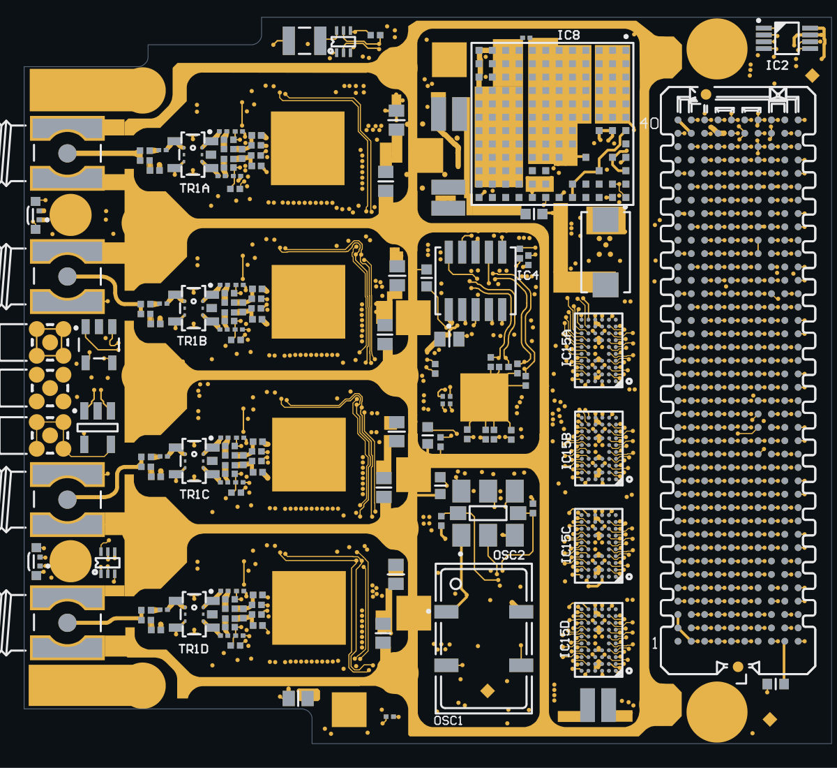
FMC ADC 130M 16B 4CHA (OHWR0019 R1) is an open-hardware circuit board from the CERN Open Hardware Repository, designed in Altium Designer: a 8-layer board of 76.8 × 69 mm with 406 components and 450 nets, published under CERN-OHL-1.1.
review 78% walked · 19 findings: 1 blocker · 9 major · 9 minor (85 items)
Open in the interactive viewerRead the full review
Design review
Probe recorded 19 findings: 1 blocker · 9 major · 9 minor (85 items) on this design. Each is shown here with its reasoning; the full review links every one to the pins, nets and datasheet pages it rests on.
- NetCopperSplitblockerOpen
NetCopperSplit: 2 boards×2
e.g. “GND's copper is in 2 pieces: R40.1 is not connected to the rest of the net” · 2 different statements
At split:GND, split:NETLABEL49
Each finding, with its own headline
split:GNDGND's copper is in 2 pieces: R40.1 is not connected to the rest of the net
GND's copper is in 2 pieces: R40.1 is not connected to the rest of the net. Piece 1: B1.1, B10.1, B11.1, B12.1, B13.1, B14.1, B15.1, B16.1 and 603 more pin(s), on TOP_LAYER, L3, L5 and BOTTOM_LAYER, 810 drill(s), 2430.23 mm2 of pour, over (-43.37, -32.79) to (32.49, 36.01). Piece 2: R40.1, on BOTTOM_LAYER, over (-43.32, -1.13) to (-39.28, 0.37). The export files every one of these pins under the net, so every connectivity check passes; the copper the fab builds leaves them apart. Usually a pour island that touches only one via of its own net, or a track ending short of its copper: join the piece to the net and export again.
split:NETLABEL49NETLABEL49's copper is in 2 pieces: J2.2 is not connected to the rest of the net
NETLABEL49's copper is in 2 pieces: J2.2 is not connected to the rest of the net. Piece 1: C43.2 and R24.2, on BOTTOM_LAYER, over (-40.77, 2.76) to (-36.78, 4.94). Piece 2: J2.2, on TOP_LAYER, L3, L5 and BOTTOM_LAYER, 1 drill(s), over (-43.31, 3.21) to (-39.27, 7.25). The export files every one of these pins under the net, so every connectivity check passes; the copper the fab builds leaves them apart. Usually a pour island that touches only one via of its own net, or a track ending short of its copper: join the piece to the net and export again.
ADC data clock and overflow flag are swapped between IC15A-D and the FMC connector: CLKOUTA reaches non-clock-capable pins, OFA reaches the CC pins
On all four channels the ADC data clock and overflow flag are swapped between IC15A-D and the FMC connector: CLKOUTA reaches non-clock-capable pins, OFA reaches the CC pins.
The crossing, channel A
The LTC2208 data-valid clock CLKOUTA (IC1A pin 41) goes through translator bit 2A10 -> 2B10 onto the net named B_OVFL_AA. The over/under-range flag OFA (pin 60) goes through 1A1 -> 1B1 onto the net named B_CLKOUTAA.
``
mermaid flowchart LR C["IC1A pin 41<br/>CLKOUTA"] -- "K5 2A10 to K2 2B10" --> N1["B_OVFL_AA<br/>J9.g30 LA29_P, not CC"] O["IC1A pin 60<br/>OFA"] -- "A6 1A1 to A1 1B1" --> N2["B_CLKOUTAA<br/>J9.d20 LA17_P_CC"]``Both translator halves have DIR tied to P1V8 (A to B) and OE to GND.
All four channels
Signal from ADC Lands on net FMC pins, channels A-D Clock-capable? CLKOUTA (pin 41) B_OVFL_Ax J9 g30, k23, h16, k11 no OFA (pin 60) B_CLKOUTAx LA17_P_CC, HA17_P_CC (k16), LA00_P_CC (g6), HA01_P_CC (e2) yes Sources
Fact Source Ball A6 (1A1) transmits to A1 (1B1); ball K5 (2A10) to K2 (2B10) SN74AVC20T245 terminal table, p.2 Pin 41 is CLKOUTA, pin 60 is OFA LTC2208 datasheet, p.14 Net-class box labels CLKOUTA beside A6 and OF_A beside K5, but the wires come from the opposite sheet ports schematic page 11 Why it matters
The schematic labels show the intended routing, the connectivity does the opposite. The carrier FPGA receives the ADC clocks on ordinary I/O. Gateware written against the net names would clock data with the overflow flag. A gateware pin map that already follows the physical wiring would hide the swap but still leaves the clocks on non-CC pins. Proposed by the walker; the owner may know of a gateware workaround.
Tantalum C35 (100uF 20V on P12V0) has no polarity mark on the silkscreen
Tantalum C35 (100 µF 20 V on the 12 V input P12V0) has no polarity mark on the silkscreen, so nothing shows the assembler which way round it goes.
What is on the board
- C35 is CTE7343-31_100UF_20V, a polarised tantalum case-D part, top side.
- The top silk shows only four symmetric corner ticks: no band, plus sign or bevel marking the anode.
- The copper footprint is symmetric too: pad 1 = P12V0, pad 2 = GND.
Why it matters
A tantalum capacitor fitted reversed on a 12 V rail fails short, often with fire, and nothing on the board tells the assembler or a reworker which way round it goes.
- PartLifecyclemajorOpen
BAR66 on D1: the distributor catalogue reports "Obsolete" for Infineon Technologies's BAR66
BAR66 on D1: the distributor catalogue reports "Obsolete" for Infineon Technologies's BAR66 — a sourcing/longevity risk to confirm against the MANUFACTURER before acting. That is the maker this board's BOM names (INFINEON). A distributor delisting is not the same claim as the part being unavailable; check the vendor's own lifecycle/product-change notice for the status and any named successor. Re-read the source: GET /api/odb/parts/BAR66/providers (which provider said it, the maker and part number it matched, its own words, and when we asked). No approved alternate is recorded for this position.
At D1
- DiffPairMismatchmajorOpen
DiffPairMismatch: 3 nets×3
3 checked by the review by Claude walker (cern session) — 2 different reasons
At HA12_N, HA13_P, LA26_P
Each finding, with its own headline
HA12_N'HA12_N' / 'HA12_P' (pair inferred from names) is pin-count asymmetric (3 vs 2)
Differential pair 'HA12_N' / 'HA12_P', INFERRED FROM THE NET NAMES (nothing in the design declares it a pair), is pin-count asymmetric (3 vs 2) - one side reaches a pin the other does not, so the two halves cannot be routed as a matched pair. NOTE: this check does not verify WHICH contact either net reaches; a correctly-symmetric pair can still be swapped at a connector.
HA13_P'HA13_P' / 'HA13_N' (pair inferred from names) is pin-count asymmetric (3 vs 1)
Differential pair 'HA13_P' / 'HA13_N', INFERRED FROM THE NET NAMES (nothing in the design declares it a pair), is pin-count asymmetric (3 vs 1) - one side reaches a pin the other does not, so the two halves cannot be routed as a matched pair. NOTE: this check does not verify WHICH contact either net reaches; a correctly-symmetric pair can still be swapped at a connector.
LA26_P'LA26_P' / 'LA26_N' (pair inferred from names) is pin-count asymmetric (2 vs 4)
Differential pair 'LA26_P' / 'LA26_N', INFERRED FROM THE NET NAMES (nothing in the design declares it a pair), is pin-count asymmetric (2 vs 4) - one side reaches a pin the other does not, so the two halves cannot be routed as a matched pair. NOTE: this check does not verify WHICH contact either net reaches; a correctly-symmetric pair can still be swapped at a connector.
- DecapOrdermajorOpen
IC8 supply pins A4, B2, B3, B4, C1, C2, C3, C4 on 'P12V0': the smallest capacitor C30 sits 3.9 mm away, behind C36 at 1.6 mm
IC8 supply pins A4, B2, B3, B4, C1, C2, C3, C4 on 'P12V0': the smallest capacitor C30 sits 3.9 mm away, behind C36 at 1.6 mm. IC8.A4: the smallest value, C30 (330 nF), is 3.9 mm from the pin and C36 (10 uF) 1.6 mm: the high-frequency part sits behind more inductance than the bulk part, which needs it least. IC8.B2: the smallest value, C30 (330 nF), is 1.9 mm from the pin and C88 (10 uF) 0.7 mm: the high-frequency part sits behind more inductance than the bulk part, which needs it least. IC8.B3: the smallest value, C30 (330 nF), is 3.0 mm from the pin and C88 (10 uF) 0.8 mm: the high-frequency part sits behind more inductance than the bulk part, which needs it least. IC8.B4: the smallest value, C30 (330 nF), is 4.1 mm from the pin and C36 (10 uF) 0.4 mm: the high-frequency part sits behind more inductance than the bulk part, which needs it least. IC8.C1: the smallest value, C30 (330 nF), is 2.6 mm from the pin and C38 (10 uF) 0.9 mm: the high-frequency part sits behind more inductance than the bulk part, which needs it least. IC8.C2: the smallest value, C30 (330 nF), is 2.9 mm from the pin and C88 (10 uF) 1.1 mm: the high-frequency part sits behind more inductance than the bulk part, which needs it least. IC8.C3: the smallest value, C30 (330 nF), is 3.7 mm from the pin and C88 (10 uF) 1.1 mm: the high-frequency part sits behind more inductance than the bulk part, which needs it least. IC8.C4: the smallest value, C30 (330 nF), is 4.7 mm from the pin and C36 (10 uF) 0.9 mm: the high-frequency part sits behind more inductance than the bulk part, which needs it least. Swap them, or bring the smallest value to the pin: it serves the fastest current and is the one the loop inductance defeats. Distances are pad centre to pin centre in the board plane. The 5 mm radius, the 10x value step and the 1 mm / 1.5x tie tolerance are Probe's starting values.
At IC8
- PartLifecyclemajorOpen
PartLifecycle: 3 part numbers×3
2 Obsolete, 1 Not For New Designs · on 9 placements
At IC13, IC15A, Q1
Each finding, with its own headline
IC13LM75AIMM/NOPB on 2 placements (IC13, IC2): the distributor catalogue reports "Obsolete" for Texas Instruments's LM75AIMM/NOPB
LM75AIMM/NOPB on 2 placements (IC13, IC2): the distributor catalogue reports "Obsolete" for Texas Instruments's LM75AIMM/NOPB — a sourcing/longevity risk to confirm against the MANUFACTURER before acting. That is the maker this board's BOM names (TEXAS INSTRUMENTS). A distributor delisting is not the same claim as the part being unavailable; check the vendor's own lifecycle/product-change notice for the status and any named successor. Re-read the source: GET /api/odb/parts/LM75AIMM/NOPB/providers (which provider said it, the maker and part number it matched, its own words, and when we asked). THE LAST BUY DATE HAS PASSED (2024-02-09, 1,010 day(s) ago), so this is a substitution rather than a buy. The distributor reports NONE left. No approved alternate is recorded for this position.
IC15ASN74AVC20T245ZQLR on 4 placements (IC15A, IC15B, IC15C, IC15D): the distributor catalogue reports "Obsolete" for Texas Instruments's SN74AVC20T245ZQLR
SN74AVC20T245ZQLR on 4 placements (IC15A, IC15B, IC15C, IC15D): the distributor catalogue reports "Obsolete" for Texas Instruments's SN74AVC20T245ZQLR — a sourcing/longevity risk to confirm against the MANUFACTURER before acting. This board's BOM names no manufacturer for it, so whether that is the fitted maker's product was not checked. A distributor delisting is not the same claim as the part being unavailable; check the vendor's own lifecycle/product-change notice for the status and any named successor. Re-read the source: GET /api/odb/parts/SN74AVC20T245ZQLR/providers (which provider said it, the maker and part number it matched, its own words, and when we asked). THE LAST BUY DATE HAS PASSED (2021-01-07, 2,138 day(s) ago), so this is a substitution rather than a buy. The distributor reports NONE left. No approved alternate is recorded for this position.
Q1PMGD280UN on 3 placements (Q1, Q2, Q5): the distributor catalogue reports "Not For New Designs" for Nexperia USA Inc.'s PMGD280UN,115
PMGD280UN on 3 placements (Q1, Q2, Q5): the distributor catalogue reports "Not For New Designs" for Nexperia USA Inc.'s PMGD280UN,115 — a sourcing/longevity risk to confirm against the MANUFACTURER before acting. This board's BOM names no manufacturer for it, so whether that is the fitted maker's product was not checked. A distributor delisting is not the same claim as the part being unavailable; check the vendor's own lifecycle/product-change notice for the status and any named successor. Re-read the source: GET /api/odb/parts/PMGD280UN/providers (which provider said it, the maker and part number it matched, its own words, and when we asked). No approved alternate is recorded for this position.
- ReferencePlaneDiscontinuitymajorOpen
ReferencePlaneDiscontinuity: 3 boards×3
Checked by the review, stands · Claude walker W3 (Cern session) — Checked: the reference break is read from the copper as stated. Whether it matters depends on the signal's edge rate and the receiver's margin, which no datasheet or app note on file fixes for this net; the impedance step and reflection figures are Probe's model, and the thresholds are its starting values. Layout practice, not a datasheet requirement. Left for the owner.
At gap:GND1:hole -44.26,-30.1|-43.25,31.92, gap:POWER:hole 5.16,5.72|7.32,7.87, split@POWER:GND|P3V3_ADC3
Each finding, with its own headline
gap:GND1:hole -44.26,-30.1|-43.25,31.922 nets cross one gap in GND1 and GND2's negative-plane field at 3 places, the longest 16.3 mm (fastest: LA16_N at 100 ps 10-90 %, ASSUMED)
Along 'NetQ2_3' on L3, GND1 is a negative layer (copper everywhere inside the profile), and its field is cleared for 16.3 mm under the track at (-43.28, 19.66). The layer does not state the nets either side, so whether this is a split between two planes or a void in one is not said; either way the return current has to go round it. 6 of them run ALONG the bare copper, parallel to its edges, rather than across it (the longest 16.21 mm). 3 places on 2 net(s) cross it, listed below, the longest first. What cleared it: the hole at x -44.26..-43.25, y -30.1..31.92. At 3 place(s) the track's plane is cleared on both sides of it, the same stretch on each reference layer: it has no plane on either side there, counted once. One decision covers the void: whether these tracks may cross it, or the plane should be filled under them. No crossing has a plane on the track's other side, so the whole return meets the break.
- one stretch, cleared on 2 reference layers: 'NetQ2_3' on L3 at (-43.28, 19.66), 16.3 mm, running ALONG the bare copper for 16.21 mm, not across it; other side: no plane on GND2 / 'NetQ2_3' on L3 at (-43.28, 19.66), 16.3 mm, running ALONG the bare copper for 16.21 mm, not across it; other side: no plane on GND1
- one stretch, cleared on 2 reference layers: 'LA16_N' on L3 at (-43.42, -20.42), 6.03 mm, running ALONG the bare copper for 5.54 mm, not across it; other side: no plane on GND2 / 'LA16_N' on L3 at (-43.42, -20.42), 6.03 mm, running ALONG the bare copper for 5.54 mm, not across it; other side: no plane on GND1
- one stretch, cleared on 2 reference layers: 'NetQ2_3' on L3 at (-43.47, -13.18), 5.94 mm, running ALONG the bare copper for 5.31 mm, not across it; other side: no plane on GND2 / 'NetQ2_3' on L3 at (-43.47, -13.18), 5.94 mm, running ALONG the bare copper for 5.31 mm, not across it; other side: no plane on GND1
Every site is a row of this finding's evidence, keyed by net, layers and position. GET /api/odb/boards/22/reference-planes?group=gap%3AGND1%3Ahole%20-44.26%2C-30.1%7C-43.25%2C31.92 serves each with its own layer_image region; all of them lie in x -44.47..-42.25, y -25.12..28.8 mm (board frame, Y up).
Read from the copper as drawn on the reference layer, along each track's centreline at exact breakpoints. The reference is the copper beside the track, never the layer's type or name. Whether it matters depends on each signal's edge rate, which nothing on file states for these nets: a slow static line crosses a split harmlessly, a fast edge does not.
gap:POWER:hole 5.16,5.72|7.32,7.873 nets cross one gap in POWER's negative-plane field at 3 places, the longest 0.27 mm (fastest: ACTIVE4_CLK_N at 1 ns 10-90 %, suggested by its name)
Along 'ACTIVE4_CLK_N' on BOTTOM_LAYER, POWER is a negative layer (copper everywhere inside the profile), and its field is cleared for 0.27 mm under the track at (5.63, 7.41). The layer does not state the nets either side, so whether this is a split between two planes or a void in one is not said; either way the return current has to go round it. 3 places on 3 net(s) cross it, listed below, the longest first. What cleared it: the hole at x 5.16..7.32, y 5.72..7.87. One decision covers the void: whether these tracks may cross it, or the plane should be filled under them. No crossing has a plane on the track's other side, so the whole return meets the break.
- 'ACTIVE4_CLK_N' on BOTTOM_LAYER at (5.63, 7.41), 0.27 mm; other side: none: the signal layer is outermost
- 'CLK0_M2C_N' on BOTTOM_LAYER at (6.16, 6.87), 0.2 mm; other side: none: the signal layer is outermost
- 'CLK0_M2C_P' on BOTTOM_LAYER at (6.44, 6.59), 0.2 mm; other side: none: the signal layer is outermost
Every site is a row of this finding's evidence, keyed by net, layers and position. GET /api/odb/boards/22/reference-planes?group=gap%3APOWER%3Ahole%205.16%2C5.72%7C7.32%2C7.87 serves each with its own layer_image region; all of them lie in x 4.59..7.51, y 5.52..8.55 mm (board frame, Y up).
Read from the copper as drawn on the reference layer, along each track's centreline at exact breakpoints. The reference is the copper beside the track, never the layer's type or name. Whether it matters depends on each signal's edge rate, which nothing on file states for these nets: a slow static line crosses a split harmlessly, a fast edge does not.
split@POWER:GND|P3V3_ADC34 nets cross the split between the GND and P3V3_ADC3 planes on POWER at 5 places, with no plane on the track's other side (fastest: NetC25C_2 at 100 ps 10-90 %, ASSUMED)
On POWER the GND and P3V3_ADC3 planes part, and 4 nets cross from one to the other at 5 place(s). The return current cannot follow a track across; it detours to wherever the two planes are joined (a stitching capacitor, or the source), and the loop it opens radiates and couples. One decision covers the boundary: whether it is stitched near these crossings, or the nets crossing it are slow enough not to care. Tracks that run ALONG this split, down the slot rather than across it, are a finding of their own: theirs is an impedance step, not a detour. At 0 of the 5 crossing(s) the track's other neighbour carries a plane, which the return can use there; 5 are on an outer layer, with no other neighbour. No crossing has a plane on the track's other side, so the whole return meets the break.
- 'ADC1_CLKC_N' on BOTTOM_LAYER at (-22.99, -2.08), 0.29 mm; other side: none: the signal layer is outermost
- 'ADC1_CLKC_P' on BOTTOM_LAYER at (-22.99, -2.63), 0.29 mm; other side: none: the signal layer is outermost
- 'NetC25C_2' on BOTTOM_LAYER at (-22.99, -0.27), 0.2 mm; other side: none: the signal layer is outermost
- 'NetC25C_2' on BOTTOM_LAYER at (-22.92, -0.9), 0.47 mm; other side: none: the signal layer is outermost
- 'VCMC' on BOTTOM_LAYER at (-23.36, -8.81), 0.32 mm; other side: none: the signal layer is outermost
Every site is a row of this finding's evidence, keyed by net, layers and position. GET /api/odb/boards/22/reference-planes?group=split%40POWER%3AGND%7CP3V3_ADC3 serves each with its own layer_image region; all of them lie in x -24.51..-21.89, y -9.81..0.73 mm (board frame, Y up).
Read from the copper as drawn on the reference layer, along each track's centreline at exact breakpoints. The reference is the copper beside the track, never the layer's type or name. Whether it matters depends on each signal's edge rate, which nothing on file states for these nets: a slow static line crosses a split harmlessly, a fast edge does not.
- ReferencePlaneDiscontinuitymajorOpen
ReferencePlaneDiscontinuity: 52 boards×52
Checked by the review, stands · Claude walker W3 (Cern session) — Checked: the reference break is read from the copper as stated. Whether it matters depends on the signal's edge rate and the receiver's margin, which no datasheet or app note on file fixes for this net; the impedance step and reflection figures are Probe's model, and the thresholds are its starting values. Layout practice, not a datasheet requirement. Left for the owner.
At gap:GND1:hole -0.33,16.86|8.19,17.07, gap:GND1:hole -1.55,16.86|-0.12,18.29, gap:GND1:hole -1.55,18.08|-1.35,36.21, gap:GND1:hole -16.88,-33.4|-15.86,-30.08, gap:GND1:hole -17.88,-31.1|-15.86,-29.08, gap:GND2:hole -0.3,16.86|8.16,17.06 and 46 more
Each finding, with its own headline
gap:GND1:hole -0.33,16.86|8.19,17.077 nets cross one gap in GND1 and GND2's negative-plane field at 7 places, the longest 4.05 mm (fastest: CH1.DA0 at 100 ps 10-90 %, ASSUMED)
Along 'CH1.DA4' on L3, GND1 is a negative layer (copper everywhere inside the profile), and its field is cleared for 4.05 mm under the track at (2.84, 17.02). The layer does not state the nets either side, so whether this is a split between two planes or a void in one is not said; either way the return current has to go round it. 4 of them run ALONG the bare copper, parallel to its edges, rather than across it (the longest 3.77 mm). 7 places on 7 net(s) cross it, listed below, the longest first. What cleared it: the hole at x -0.3..8.16, y 16.86..17.06 and the hole at x -0.33..8.19, y 16.86..17.07. At 7 place(s) the track's plane is cleared on both sides of it, the same stretch on each reference layer: it has no plane on either side there, counted once. One decision covers the void: whether these tracks may cross it, or the plane should be filled under them. No crossing has a plane on the track's other side, so the whole return meets the break.
- one stretch, cleared on 2 reference layers: 'CH1.DA4' on L3 at (2.84, 17.02), 4.05 mm, running ALONG the bare copper for 3.77 mm, not across it; other side: no plane on GND2 / 'CH1.DA4' on L3 at (2.84, 17.02), 4.05 mm, running ALONG the bare copper for 3.77 mm, not across it; other side: no plane on GND1
- one stretch, cleared on 2 reference layers: 'CH1.DA5' on L3 at (0.28, 16.99), 1.28 mm, running ALONG the bare copper for 0.91 mm, not across it; other side: no plane on GND2 / 'CH1.DA5' on L3 at (0.3, 16.99), 1.26 mm, running ALONG the bare copper for 0.88 mm, not across it; other side: no plane on GND1
- one stretch, cleared on 2 reference layers: 'CH1.CLKOUTA' on L3 at (6.33, 16.97), 0.29 mm; other side: no plane on GND2 / 'CH1.CLKOUTA' on L3 at (6.34, 16.96), 0.29 mm; other side: no plane on GND1
- one stretch, cleared on 2 reference layers: 'CH1.DA0' on L3 at (6.01, 16.97), 0.29 mm; other side: no plane on GND2 / 'CH1.DA0' on L3 at (6.01, 16.96), 0.29 mm; other side: no plane on GND1
- one stretch, cleared on 2 reference layers: 'CH1.DA1' on L3 at (5.68, 16.97), 0.29 mm; other side: no plane on GND2 / 'CH1.DA1' on L3 at (5.69, 16.96), 0.29 mm; other side: no plane on GND1
- one stretch, cleared on 2 reference layers: 'CH1.DA2' on L3 at (5.36, 16.97), 0.29 mm; other side: no plane on GND2 / 'CH1.DA2' on L3 at (5.37, 16.96), 0.29 mm; other side: no plane on GND1
- one stretch, cleared on 2 reference layers: 'CH1.DA3' on L3 at (5.06, 16.97), 0.29 mm; other side: no plane on GND2 / 'CH1.DA3' on L3 at (5.07, 16.96), 0.29 mm; other side: no plane on GND1
Every site is a row of this finding's evidence, keyed by net, layers and position. GET /api/odb/boards/22/reference-planes?group=gap%3AGND1%3Ahole%20-0.33%2C16.86%7C8.19%2C17.07 serves each with its own layer_image region; all of them lie in x -1.4..7.44, y 15.86..18.07 mm (board frame, Y up).
Read from the copper as drawn on the reference layer, along each track's centreline at exact breakpoints. The reference is the copper beside the track, never the layer's type or name. Whether it matters depends on each signal's edge rate, which nothing on file states for these nets: a slow static line crosses a split harmlessly, a fast edge does not.
gap:GND1:hole -1.55,16.86|-0.12,18.295 nets cross one gap in GND1 and GND2's negative-plane field at 5 places, the longest 0.29 mm (fastest: CH1.DA0 at 100 ps 10-90 %, ASSUMED)
Along 'CH1.DA0' on L3, GND1 is a negative layer (copper everywhere inside the profile), and its field is cleared for 0.29 mm under the track at (-1.3, 18.03). The layer does not state the nets either side, so whether this is a split between two planes or a void in one is not said; either way the return current has to go round it. 5 places on 5 net(s) cross it, listed below, the longest first. What cleared it: the hole at x -1.55..-0.09, y 16.86..18.31 and the hole at x -1.55..-0.12, y 16.86..18.29. At 5 place(s) the track's plane is cleared on both sides of it, the same stretch on each reference layer: it has no plane on either side there, counted once. One decision covers the void: whether these tracks may cross it, or the plane should be filled under them. No crossing has a plane on the track's other side, so the whole return meets the break.
- one stretch, cleared on 2 reference layers: 'CH1.DA0' on L3 at (-1.3, 18.03), 0.29 mm; other side: no plane on GND2 / 'CH1.DA0' on L3 at (-1.27, 18.03), 0.29 mm; other side: no plane on GND1
- one stretch, cleared on 2 reference layers: 'CH1.DA1' on L3 at (-1.07, 17.81), 0.29 mm; other side: no plane on GND2 / 'CH1.DA1' on L3 at (-1.04, 17.81), 0.29 mm; other side: no plane on GND1
- one stretch, cleared on 2 reference layers: 'CH1.DA2' on L3 at (-0.86, 17.6), 0.29 mm; other side: no plane on GND2 / 'CH1.DA2' on L3 at (-0.84, 17.6), 0.29 mm; other side: no plane on GND1
- one stretch, cleared on 2 reference layers: 'CH1.DA3' on L3 at (-0.66, 17.4), 0.29 mm; other side: no plane on GND2 / 'CH1.DA3' on L3 at (-0.64, 17.4), 0.29 mm; other side: no plane on GND1
- one stretch, cleared on 2 reference layers: 'CH1.DA4' on L3 at (-0.46, 17.2), 0.29 mm; other side: no plane on GND2 / 'CH1.DA4' on L3 at (-0.43, 17.2), 0.29 mm; other side: no plane on GND1
Every site is a row of this finding's evidence, keyed by net, layers and position. GET /api/odb/boards/22/reference-planes?group=gap%3AGND1%3Ahole%20-1.55%2C16.86%7C-0.12%2C18.29 serves each with its own layer_image region; all of them lie in x -2.44..0.71, y 16.2..19.03 mm (board frame, Y up).
Read from the copper as drawn on the reference layer, along each track's centreline at exact breakpoints. The reference is the copper beside the track, never the layer's type or name. Whether it matters depends on each signal's edge rate, which nothing on file states for these nets: a slow static line crosses a split harmlessly, a fast edge does not.
gap:GND1:hole -1.55,18.08|-1.35,36.216 nets cross one gap in GND1 and GND2's negative-plane field at 6 places, the longest 0.2 mm (fastest: LA26_N at 100 ps 10-90 %, ASSUMED)
Along 'LA26_P' on L3, GND2 is a negative layer (copper everywhere inside the profile), and its field is cleared for 0.2 mm under the track at (-1.45, 33.77). The layer does not state the nets either side, so whether this is a split between two planes or a void in one is not said; either way the return current has to go round it. 6 places on 6 net(s) cross it, listed below, the longest first. What cleared it: the hole at x -1.55..-1.35, y 18.08..36.21 and the hole at x -1.55..-1.35, y 18.11..35.84. At 6 place(s) the track's plane is cleared on both sides of it, the same stretch on each reference layer: it has no plane on either side there, counted once. One decision covers the void: whether these tracks may cross it, or the plane should be filled under them. No crossing has a plane on the track's other side, so the whole return meets the break.
- one stretch, cleared on 2 reference layers: 'CH1.CLKOUTA' on L3 at (-1.45, 18.26), 0.2 mm; other side: no plane on GND2 / 'CH1.CLKOUTA' on L3 at (-1.45, 18.26), 0.2 mm; other side: no plane on GND1
- one stretch, cleared on 2 reference layers: 'LA26_N' on L3 at (-1.45, 34), 0.2 mm; other side: no plane on GND2 / 'LA26_N' on L3 at (-1.45, 34), 0.2 mm; other side: no plane on GND1
- one stretch, cleared on 2 reference layers: 'LA26_P' on L3 at (-1.45, 33.77), 0.2 mm; other side: no plane on GND2 / 'LA26_P' on L3 at (-1.45, 33.77), 0.2 mm; other side: no plane on GND1
- one stretch, cleared on 2 reference layers: 'LA28_P' on L3 at (-1.45, 34.23), 0.2 mm; other side: no plane on GND2 / 'LA28_P' on L3 at (-1.45, 34.23), 0.2 mm; other side: no plane on GND1
- one stretch, cleared on 2 reference layers: 'LA32_N' on L3 at (-1.45, 34.5), 0.2 mm; other side: no plane on GND2 / 'LA32_N' on L3 at (-1.45, 34.5), 0.2 mm; other side: no plane on GND1
- one stretch, cleared on 2 reference layers: 'LA32_P' on L3 at (-1.45, 34.88), 0.2 mm; other side: no plane on GND2 / 'LA32_P' on L3 at (-1.45, 34.88), 0.2 mm; other side: no plane on GND1
Every site is a row of this finding's evidence, keyed by net, layers and position. GET /api/odb/boards/22/reference-planes?group=gap%3AGND1%3Ahole%20-1.55%2C18.08%7C-1.35%2C36.21 serves each with its own layer_image region; all of them lie in x -2.55..-0.35, y 17.26..35.88 mm (board frame, Y up).
Read from the copper as drawn on the reference layer, along each track's centreline at exact breakpoints. The reference is the copper beside the track, never the layer's type or name. Whether it matters depends on each signal's edge rate, which nothing on file states for these nets: a slow static line crosses a split harmlessly, a fast edge does not.
gap:GND1:hole -16.88,-33.4|-15.86,-30.08'LA16_N' crosses one gap in GND1 and GND2's negative-plane field at 1 place, the longest 42.67 mm (fastest: LA16_N at 100 ps 10-90 %, ASSUMED)
Along 'LA16_N' on L3, GND1 is a negative layer (copper everywhere inside the profile), and its field is cleared for 42.67 mm under the track at (5.7, -32.59). The layer does not state the nets either side, so whether this is a split between two planes or a void in one is not said; either way the return current has to go round it. 4 of them run ALONG the bare copper, parallel to its edges, rather than across it (the longest 42.07 mm). What cleared it: the hole at x -16.88..-15.86, y -33.4..-30.08 and the hole at x -16.88..33.54, y -33.4..-32.38. At 1 place(s) the track's plane is cleared on both sides of it, the same stretch on each reference layer: it has no plane on either side there, counted once. One decision covers the void: whether these tracks may cross it, or the plane should be filled under them. No crossing has a plane on the track's other side, so the whole return meets the break.
- one stretch, cleared on 4 reference layers: 'LA16_N' on L3 at (-15.96, -31.43), 2.05 mm, running ALONG the bare copper for 1.54 mm, not across it; other side: no plane on GND2 / 'LA16_N' on L3 at (5.7, -32.59), 42.67 mm, running ALONG the bare copper for 42.07 mm, not across it; other side: no plane on GND2 / 'LA16_N' on L3 at (-15.96, -31.43), 2.05 mm, running ALONG the bare copper for 1.54 mm, not across it; other side: no plane on GND1 / 'LA16_N' on L3 at (5.7, -32.59), 42.67 mm, running ALONG the bare copper for 42.07 mm, not across it; other side: no plane on GND1
Every site is a row of this finding's evidence, keyed by net, layers and position. GET /api/odb/boards/22/reference-planes?group=gap%3AGND1%3Ahole%20-16.88%2C-33.4%7C-15.86%2C-30.08 serves each with its own layer_image region; all of them lie in x -16.96..27.95, y -33.59..-29.05 mm (board frame, Y up).
Read from the copper as drawn on the reference layer, along each track's centreline at exact breakpoints. The reference is the copper beside the track, never the layer's type or name. Whether it matters depends on each signal's edge rate, which nothing on file states for these nets: a slow static line crosses a split harmlessly, a fast edge does not.
gap:GND1:hole -17.88,-31.1|-15.86,-29.08'LA16_N' crosses one gap in GND1 and GND2's negative-plane field at 1 place, the longest 1.14 mm (fastest: LA16_N at 100 ps 10-90 %, ASSUMED)
Along 'LA16_N' on L3, GND1 is a negative layer (copper everywhere inside the profile), and its field is cleared for 1.14 mm under the track at (-16.39, -29.6). The layer does not state the nets either side, so whether this is a split between two planes or a void in one is not said; either way the return current has to go round it. 2 of them run ALONG the bare copper, parallel to its edges, rather than across it (the longest 0.12 mm). What cleared it: the hole at x -17.88..-15.86, y -31.1..-29.08. At 1 place(s) the track's plane is cleared on both sides of it, the same stretch on each reference layer: it has no plane on either side there, counted once. One decision covers the void: whether these tracks may cross it, or the plane should be filled under them. No crossing has a plane on the track's other side, so the whole return meets the break.
- one stretch, cleared on 2 reference layers: 'LA16_N' on L3 at (-16.39, -29.6), 1.14 mm, running ALONG the bare copper for 0.12 mm, not across it; other side: no plane on GND2 / 'LA16_N' on L3 at (-16.39, -29.6), 1.14 mm, running ALONG the bare copper for 0.12 mm, not across it; other side: no plane on GND1
Every site is a row of this finding's evidence, keyed by net, layers and position. GET /api/odb/boards/22/reference-planes?group=gap%3AGND1%3Ahole%20-17.88%2C-31.1%7C-15.86%2C-29.08 serves each with its own layer_image region; all of them lie in x -17.79..-14.98, y -31.01..-28.2 mm (board frame, Y up).
Read from the copper as drawn on the reference layer, along each track's centreline at exact breakpoints. The reference is the copper beside the track, never the layer's type or name. Whether it matters depends on each signal's edge rate, which nothing on file states for these nets: a slow static line crosses a split harmlessly, a fast edge does not.
gap:GND2:hole -0.3,16.86|8.16,17.06'REF_P' crosses one gap in GND2 and GND3's negative-plane field at 1 place, the longest 0.29 mm (fastest: REF_P at 100 ps 10-90 %, ASSUMED)
Along 'REF_P' on L5, GND2 is a negative layer (copper everywhere inside the profile), and its field is cleared for 0.29 mm under the track at (7.61, 16.96). The layer does not state the nets either side, so whether this is a split between two planes or a void in one is not said; either way the return current has to go round it. What cleared it: the hole at x -0.3..8.16, y 16.86..17.06 and the hole at x -0.33..8.19, y 16.91..17.11. At 1 place(s) the track's plane is cleared on both sides of it, the same stretch on each reference layer: it has no plane on either side there, counted once. One decision covers the void: whether these tracks may cross it, or the plane should be filled under them. No crossing has a plane on the track's other side, so the whole return meets the break.
- one stretch, cleared on 2 reference layers: 'REF_P' on L5 at (7.61, 16.96), 0.29 mm; other side: no plane on GND3 / 'REF_P' on L5 at (7.67, 17.01), 0.29 mm; other side: no plane on GND2
Every site is a row of this finding's evidence, keyed by net, layers and position. GET /api/odb/boards/22/reference-planes?group=gap%3AGND2%3Ahole%20-0.3%2C16.86%7C8.16%2C17.06 serves each with its own layer_image region; all of them lie in x 6.51..8.77, y 15.86..18.11 mm (board frame, Y up).
Read from the copper as drawn on the reference layer, along each track's centreline at exact breakpoints. The reference is the copper beside the track, never the layer's type or name. Whether it matters depends on each signal's edge rate, which nothing on file states for these nets: a slow static line crosses a split harmlessly, a fast edge does not.
gap:GND2:hole 14.3,17.78|14.5,26.49'LA31_N' crosses one gap in GND2 and GND3's negative-plane field at 1 place, the longest 0.2 mm (fastest: LA31_N at 100 ps 10-90 %, ASSUMED)
Along 'LA31_N' on L5, GND2 is a negative layer (copper everywhere inside the profile), and its field is cleared for 0.2 mm under the track at (14.4, 21.08). The layer does not state the nets either side, so whether this is a split between two planes or a void in one is not said; either way the return current has to go round it. What cleared it: the hole at x 14.3..14.5, y 17.78..26.49 and the hole at x 14.3..14.5, y 17.81..26.57. At 1 place(s) the track's plane is cleared on both sides of it, the same stretch on each reference layer: it has no plane on either side there, counted once. One decision covers the void: whether these tracks may cross it, or the plane should be filled under them. No crossing has a plane on the track's other side, so the whole return meets the break.
- one stretch, cleared on 2 reference layers: 'LA31_N' on L5 at (14.4, 21.08), 0.2 mm; other side: no plane on GND3 / 'LA31_N' on L5 at (14.4, 21.08), 0.2 mm; other side: no plane on GND2
Every site is a row of this finding's evidence, keyed by net, layers and position. GET /api/odb/boards/22/reference-planes?group=gap%3AGND2%3Ahole%2014.3%2C17.78%7C14.5%2C26.49 serves each with its own layer_image region; all of them lie in x 13.3..15.5, y 20.08..22.08 mm (board frame, Y up).
Read from the copper as drawn on the reference layer, along each track's centreline at exact breakpoints. The reference is the copper beside the track, never the layer's type or name. Whether it matters depends on each signal's edge rate, which nothing on file states for these nets: a slow static line crosses a split harmlessly, a fast edge does not.
gap:GND2:hole 7.95,16.86|9.18,18.08'REF_N' crosses one gap in GND2 and GND3's negative-plane field at 1 place, the longest 1.15 mm (fastest: REF_N at 100 ps 10-90 %, ASSUMED)
Along 'REF_N' on L5, GND2 is a negative layer (copper everywhere inside the profile), and its field is cleared for 1.15 mm under the track at (8.46, 17.25). The layer does not state the nets either side, so whether this is a split between two planes or a void in one is not said; either way the return current has to go round it. 2 of them run ALONG the bare copper, parallel to its edges, rather than across it (the longest 1.04 mm). What cleared it: the hole at x 7.95..9.18, y 16.86..18.08 and the hole at x 7.99..9.18, y 16.91..18.11. At 1 place(s) the track's plane is cleared on both sides of it, the same stretch on each reference layer: it has no plane on either side there, counted once. One decision covers the void: whether these tracks may cross it, or the plane should be filled under them. No crossing has a plane on the track's other side, so the whole return meets the break.
- one stretch, cleared on 2 reference layers: 'REF_N' on L5 at (8.46, 17.25), 1.15 mm, running ALONG the bare copper for 0.98 mm, not across it; other side: no plane on GND3 / 'REF_N' on L5 at (8.49, 17.28), 1.05 mm, running ALONG the bare copper for 1.04 mm, not across it; other side: no plane on GND2
Every site is a row of this finding's evidence, keyed by net, layers and position. GET /api/odb/boards/22/reference-planes?group=gap%3AGND2%3Ahole%207.95%2C16.86%7C9.18%2C18.08 serves each with its own layer_image region; all of them lie in x 7.06..9.89, y 15.86..18.65 mm (board frame, Y up).
Read from the copper as drawn on the reference layer, along each track's centreline at exact breakpoints. The reference is the copper beside the track, never the layer's type or name. Whether it matters depends on each signal's edge rate, which nothing on file states for these nets: a slow static line crosses a split harmlessly, a fast edge does not.
gap:GND2:hole 8.95,17.86|14.48,18.11'REF_P' crosses one gap in GND2 and GND3's negative-plane field at 1 place, the longest 0.99 mm (fastest: REF_P at 100 ps 10-90 %, ASSUMED)
Along 'REF_P' on L5, GND3 is a negative layer (copper everywhere inside the profile), and its field is cleared for 0.99 mm under the track at (10.65, 18.04). The layer does not state the nets either side, so whether this is a split between two planes or a void in one is not said; either way the return current has to go round it. 2 of them run ALONG the bare copper, parallel to its edges, rather than across it (the longest 0.63 mm). What cleared it: the hole at x 8.95..14.48, y 17.86..18.11 and the hole at x 8.96..14.46, y 17.88..18.14. At 1 place(s) the track's plane is cleared on both sides of it, the same stretch on each reference layer: it has no plane on either side there, counted once. One decision covers the void: whether these tracks may cross it, or the plane should be filled under them. No crossing has a plane on the track's other side, so the whole return meets the break.
- one stretch, cleared on 2 reference layers: 'REF_P' on L5 at (10.65, 18.04), 0.99 mm, running ALONG the bare copper for 0.63 mm, not across it; other side: no plane on GND3 / 'REF_P' on L5 at (10.65, 18.04), 0.99 mm, running ALONG the bare copper for 0.63 mm, not across it; other side: no plane on GND2
Every site is a row of this finding's evidence, keyed by net, layers and position. GET /api/odb/boards/22/reference-planes?group=gap%3AGND2%3Ahole%208.95%2C17.86%7C14.48%2C18.11 serves each with its own layer_image region; all of them lie in x 9.24..12.15, y 16.86..19.14 mm (board frame, Y up).
Read from the copper as drawn on the reference layer, along each track's centreline at exact breakpoints. The reference is the copper beside the track, never the layer's type or name. Whether it matters depends on each signal's edge rate, which nothing on file states for these nets: a slow static line crosses a split harmlessly, a fast edge does not.
gap:POWER:hole -0.81,14.15|2.13,17.09'RF6' crosses one gap in POWER's negative-plane field at 1 place, the longest 0.29 mm (fastest: RF6 at 100 ps 10-90 %, ASSUMED)
Along 'RF6' on BOTTOM_LAYER, POWER is a negative layer (copper everywhere inside the profile), and its field is cleared for 0.29 mm under the track at (1.68, 14.61). The layer does not state the nets either side, so whether this is a split between two planes or a void in one is not said; either way the return current has to go round it. What cleared it: the hole at x -0.81..2.13, y 14.15..17.09. One decision covers the void: whether these tracks may cross it, or the plane should be filled under them. No crossing has a plane on the track's other side, so the whole return meets the break.
- 'RF6' on BOTTOM_LAYER at (1.68, 14.61), 0.29 mm; other side: none: the signal layer is outermost
Every site is a row of this finding's evidence, keyed by net, layers and position. GET /api/odb/boards/22/reference-planes?group=gap%3APOWER%3Ahole%20-0.81%2C14.15%7C2.13%2C17.09 serves each with its own layer_image region; all of them lie in x 0.68..2.68, y 13.46..15.75 mm (board frame, Y up).
Read from the copper as drawn on the reference layer, along each track's centreline at exact breakpoints. The reference is the copper beside the track, never the layer's type or name. Whether it matters depends on each signal's edge rate, which nothing on file states for these nets: a slow static line crosses a split harmlessly, a fast edge does not.
gap:POWER:hole -2.11,14.12|-0,14.33'ACTIVE1_CLK_P' crosses one gap in POWER's negative-plane field at 1 place, the longest 0.24 mm (fastest: ACTIVE1_CLK_P at 1 ns 10-90 %, suggested by its name)
Along 'ACTIVE1_CLK_P' on BOTTOM_LAYER, POWER is a negative layer (copper everywhere inside the profile), and its field is cleared for 0.24 mm under the track at (-1.29, 14.17). The layer does not state the nets either side, so whether this is a split between two planes or a void in one is not said; either way the return current has to go round it. What cleared it: the hole at x -2.11..-0, y 14.12..14.33. One decision covers the void: whether these tracks may cross it, or the plane should be filled under them. No crossing has a plane on the track's other side, so the whole return meets the break.
- 'ACTIVE1_CLK_P' on BOTTOM_LAYER at (-1.29, 14.17), 0.24 mm; other side: none: the signal layer is outermost
Every site is a row of this finding's evidence, keyed by net, layers and position. GET /api/odb/boards/22/reference-planes?group=gap%3APOWER%3Ahole%20-2.11%2C14.12%7C-0%2C14.33 serves each with its own layer_image region; all of them lie in x -2.34..-0.25, y 13.12..15.33 mm (board frame, Y up).
Read from the copper as drawn on the reference layer, along each track's centreline at exact breakpoints. The reference is the copper beside the track, never the layer's type or name. Whether it matters depends on each signal's edge rate, which nothing on file states for these nets: a slow static line crosses a split harmlessly, a fast edge does not.
gap:POWER:hole -20.48,17.12|-10.57,17.32'DITH_ON_OFF' crosses one gap in POWER's negative-plane field at 1 place, the longest 0.29 mm (fastest: DITH_ON_OFF at 100 ps 10-90 %, ASSUMED)
Along 'DITH_ON_OFF' on BOTTOM_LAYER, POWER is a negative layer (copper everywhere inside the profile), and its field is cleared for 0.29 mm under the track at (-11.13, 17.22). The layer does not state the nets either side, so whether this is a split between two planes or a void in one is not said; either way the return current has to go round it. What cleared it: the hole at x -20.48..-10.57, y 17.12..17.32. One decision covers the void: whether these tracks may cross it, or the plane should be filled under them. No crossing has a plane on the track's other side, so the whole return meets the break.
- 'DITH_ON_OFF' on BOTTOM_LAYER at (-11.13, 17.22), 0.29 mm; other side: none: the signal layer is outermost
Every site is a row of this finding's evidence, keyed by net, layers and position. GET /api/odb/boards/22/reference-planes?group=gap%3APOWER%3Ahole%20-20.48%2C17.12%7C-10.57%2C17.32 serves each with its own layer_image region; all of them lie in x -12.23..-10.02, y 16.12..18.32 mm (board frame, Y up).
Read from the copper as drawn on the reference layer, along each track's centreline at exact breakpoints. The reference is the copper beside the track, never the layer's type or name. Whether it matters depends on each signal's edge rate, which nothing on file states for these nets: a slow static line crosses a split harmlessly, a fast edge does not.
gap:POWER:hole -3.3,14.12|-1.91,15.52'PASSIVE1_CLK_P' crosses one gap in POWER's negative-plane field at 1 place, the longest 0.2 mm (fastest: PASSIVE1_CLK_P at 1 ns 10-90 %, suggested by its name)
Along 'PASSIVE1_CLK_P' on BOTTOM_LAYER, POWER is a negative layer (copper everywhere inside the profile), and its field is cleared for 0.2 mm under the track at (-2.24, 14.45). The layer does not state the nets either side, so whether this is a split between two planes or a void in one is not said; either way the return current has to go round it. What cleared it: the hole at x -3.3..-1.91, y 14.12..15.52. One decision covers the void: whether these tracks may cross it, or the plane should be filled under them. No crossing has a plane on the track's other side, so the whole return meets the break.
- 'PASSIVE1_CLK_P' on BOTTOM_LAYER at (-2.24, 14.45), 0.2 mm; other side: none: the signal layer is outermost
Every site is a row of this finding's evidence, keyed by net, layers and position. GET /api/odb/boards/22/reference-planes?group=gap%3APOWER%3Ahole%20-3.3%2C14.12%7C-1.91%2C15.52 serves each with its own layer_image region; all of them lie in x -3.31..-1.16, y 13.38..15.52 mm (board frame, Y up).
Read from the copper as drawn on the reference layer, along each track's centreline at exact breakpoints. The reference is the copper beside the track, never the layer's type or name. Whether it matters depends on each signal's edge rate, which nothing on file states for these nets: a slow static line crosses a split harmlessly, a fast edge does not.
gap:POWER:hole -4.27,-20.8|-4.06,-12.4'NetC55_2' crosses one gap in POWER's negative-plane field at 1 place, the longest 0.2 mm (fastest: NetC55_2 at 100 ps 10-90 %, ASSUMED)
Along 'NetC55_2' on BOTTOM_LAYER, POWER is a negative layer (copper everywhere inside the profile), and its field is cleared for 0.2 mm under the track at (-4.17, -14.16). The layer does not state the nets either side, so whether this is a split between two planes or a void in one is not said; either way the return current has to go round it. What cleared it: the hole at x -4.27..-4.06, y -20.8..-12.4. One decision covers the void: whether these tracks may cross it, or the plane should be filled under them. No crossing has a plane on the track's other side, so the whole return meets the break.
- 'NetC55_2' on BOTTOM_LAYER at (-4.17, -14.16), 0.2 mm; other side: none: the signal layer is outermost
Every site is a row of this finding's evidence, keyed by net, layers and position. GET /api/odb/boards/22/reference-planes?group=gap%3APOWER%3Ahole%20-4.27%2C-20.8%7C-4.06%2C-12.4 serves each with its own layer_image region; all of them lie in x -5.27..-3.06, y -15.16..-13.16 mm (board frame, Y up).
Read from the copper as drawn on the reference layer, along each track's centreline at exact breakpoints. The reference is the copper beside the track, never the layer's type or name. Whether it matters depends on each signal's edge rate, which nothing on file states for these nets: a slow static line crosses a split harmlessly, a fast edge does not.
gap:POWER:hole -4.27,-21.21|-3.66,-20.6'NetC102_2' crosses one gap in POWER's negative-plane field at 1 place, the longest 0.26 mm (fastest: NetC102_2 at 100 ps 10-90 %, ASSUMED)
Along 'NetC102_2' on BOTTOM_LAYER, POWER is a negative layer (copper everywhere inside the profile), and its field is cleared for 0.26 mm under the track at (-3.76, -21.15). The layer does not state the nets either side, so whether this is a split between two planes or a void in one is not said; either way the return current has to go round it. What cleared it: the hole at x -4.27..-3.66, y -21.21..-20.6. One decision covers the void: whether these tracks may cross it, or the plane should be filled under them. No crossing has a plane on the track's other side, so the whole return meets the break.
- 'NetC102_2' on BOTTOM_LAYER at (-3.76, -21.15), 0.26 mm; other side: none: the signal layer is outermost
Every site is a row of this finding's evidence, keyed by net, layers and position. GET /api/odb/boards/22/reference-planes?group=gap%3APOWER%3Ahole%20-4.27%2C-21.21%7C-3.66%2C-20.6 serves each with its own layer_image region; all of them lie in x -4.86..-2.6, y -22.15..-20.15 mm (board frame, Y up).
Read from the copper as drawn on the reference layer, along each track's centreline at exact breakpoints. The reference is the copper beside the track, never the layer's type or name. Whether it matters depends on each signal's edge rate, which nothing on file states for these nets: a slow static line crosses a split harmlessly, a fast edge does not.
gap:POWER:hole 11.89,-26.37|12.09,10.64'CLK0_M2C_P' crosses one gap in POWER's negative-plane field at 1 place, the longest 0.2 mm (fastest: CLK0_M2C_P at 1 ns 10-90 %, suggested by its name)
Along 'CLK0_M2C_P' on BOTTOM_LAYER, POWER is a negative layer (copper everywhere inside the profile), and its field is cleared for 0.2 mm under the track at (11.99, 10.26). The layer does not state the nets either side, so whether this is a split between two planes or a void in one is not said; either way the return current has to go round it. What cleared it: the hole at x 11.89..12.09, y -26.37..10.64. One decision covers the void: whether these tracks may cross it, or the plane should be filled under them. No crossing has a plane on the track's other side, so the whole return meets the break.
- 'CLK0_M2C_P' on BOTTOM_LAYER at (11.99, 10.26), 0.2 mm; other side: none: the signal layer is outermost
Every site is a row of this finding's evidence, keyed by net, layers and position. GET /api/odb/boards/22/reference-planes?group=gap%3APOWER%3Ahole%2011.89%2C-26.37%7C12.09%2C10.64 serves each with its own layer_image region; all of them lie in x 10.89..13.09, y 9.26..11.26 mm (board frame, Y up).
Read from the copper as drawn on the reference layer, along each track's centreline at exact breakpoints. The reference is the copper beside the track, never the layer's type or name. Whether it matters depends on each signal's edge rate, which nothing on file states for these nets: a slow static line crosses a split harmlessly, a fast edge does not.
gap:POWER:hole 11.89,10.44|14.25,12.8'CLK0_M2C_N' crosses one gap in POWER's negative-plane field at 1 place, the longest 0.53 mm (fastest: CLK0_M2C_N at 1 ns 10-90 %, suggested by its name)
Along 'CLK0_M2C_N' on BOTTOM_LAYER, POWER is a negative layer (copper everywhere inside the profile), and its field is cleared for 0.53 mm under the track at (12.11, 10.66). The layer does not state the nets either side, so whether this is a split between two planes or a void in one is not said; either way the return current has to go round it. What cleared it: the hole at x 11.89..14.25, y 10.44..12.8. One decision covers the void: whether these tracks may cross it, or the plane should be filled under them. No crossing has a plane on the track's other side, so the whole return meets the break.
- 'CLK0_M2C_N' on BOTTOM_LAYER at (12.11, 10.66), 0.53 mm; other side: none: the signal layer is outermost
Every site is a row of this finding's evidence, keyed by net, layers and position. GET /api/odb/boards/22/reference-planes?group=gap%3APOWER%3Ahole%2011.89%2C10.44%7C14.25%2C12.8 serves each with its own layer_image region; all of them lie in x 10.73..13.25, y 9.66..11.66 mm (board frame, Y up).
Read from the copper as drawn on the reference layer, along each track's centreline at exact breakpoints. The reference is the copper beside the track, never the layer's type or name. Whether it matters depends on each signal's edge rate, which nothing on file states for these nets: a slow static line crosses a split harmlessly, a fast edge does not.
gap:POWER:hole 3.18,-23.85|3.78,-23.24'NetOSC1_3' crosses one gap in POWER's negative-plane field at 1 place, the longest 0.54 mm (fastest: NetOSC1_3 at 1 ns 10-90 %, suggested by its name)
Along 'NetOSC1_3' on BOTTOM_LAYER, POWER is a negative layer (copper everywhere inside the profile), and its field is cleared for 0.54 mm under the track at (3.59, -23.44). The layer does not state the nets either side, so whether this is a split between two planes or a void in one is not said; either way the return current has to go round it. What cleared it: the hole at x 3.18..3.78, y -23.85..-23.24. One decision covers the void: whether these tracks may cross it, or the plane should be filled under them. No crossing has a plane on the track's other side, so the whole return meets the break.
- 'NetOSC1_3' on BOTTOM_LAYER at (3.59, -23.44), 0.54 mm; other side: none: the signal layer is outermost
Every site is a row of this finding's evidence, keyed by net, layers and position. GET /api/odb/boards/22/reference-planes?group=gap%3APOWER%3Ahole%203.18%2C-23.85%7C3.78%2C-23.24 serves each with its own layer_image region; all of them lie in x 2.48..4.86, y -24.55..-22.16 mm (board frame, Y up).
Read from the copper as drawn on the reference layer, along each track's centreline at exact breakpoints. The reference is the copper beside the track, never the layer's type or name. Whether it matters depends on each signal's edge rate, which nothing on file states for these nets: a slow static line crosses a split harmlessly, a fast edge does not.
gap:POWER:hole 3.84,-21.59|5.13,-20.29'NetOSC1_3' crosses one gap in POWER's negative-plane field at 1 place, the longest 0.29 mm (fastest: NetOSC1_3 at 1 ns 10-90 %, suggested by its name)
Along 'NetOSC1_3' on BOTTOM_LAYER, POWER is a negative layer (copper everywhere inside the profile), and its field is cleared for 0.29 mm under the track at (4.24, -21.18). The layer does not state the nets either side, so whether this is a split between two planes or a void in one is not said; either way the return current has to go round it. What cleared it: the hole at x 3.84..5.13, y -21.59..-20.29. One decision covers the void: whether these tracks may cross it, or the plane should be filled under them. No crossing has a plane on the track's other side, so the whole return meets the break.
- 'NetOSC1_3' on BOTTOM_LAYER at (4.24, -21.18), 0.29 mm; other side: none: the signal layer is outermost
Every site is a row of this finding's evidence, keyed by net, layers and position. GET /api/odb/boards/22/reference-planes?group=gap%3APOWER%3Ahole%203.84%2C-21.59%7C5.13%2C-20.29 serves each with its own layer_image region; all of them lie in x 3.24..5.24, y -22.33..-20.04 mm (board frame, Y up).
Read from the copper as drawn on the reference layer, along each track's centreline at exact breakpoints. The reference is the copper beside the track, never the layer's type or name. Whether it matters depends on each signal's edge rate, which nothing on file states for these nets: a slow static line crosses a split harmlessly, a fast edge does not.
gap:POWER:hole 4.93,-6.32|7.32,-3.942 nets cross one gap in POWER's negative-plane field at 3 places, the longest 0.29 mm (fastest: RF_AUX_N at 100 ps 10-90 %, ASSUMED)
Along 'RF_AUX_P' on BOTTOM_LAYER, POWER is a negative layer (copper everywhere inside the profile), and its field is cleared for 0.29 mm under the track at (5.88, -5.33). The layer does not state the nets either side, so whether this is a split between two planes or a void in one is not said; either way the return current has to go round it. 3 places on 2 net(s) cross it, listed below, the longest first. What cleared it: the hole at x 4.93..7.32, y -6.32..-3.94. One decision covers the void: whether these tracks may cross it, or the plane should be filled under them. No crossing has a plane on the track's other side, so the whole return meets the break.
- 'RF_AUX_P' on BOTTOM_LAYER at (5.88, -5.33), 0.29 mm; other side: none: the signal layer is outermost
- 'RF_AUX_N' on BOTTOM_LAYER at (5.57, -5.72), 0.29 mm; other side: none: the signal layer is outermost
- 'RF_AUX_P' on BOTTOM_LAYER at (6.88, -4.36), 0.29 mm; other side: none: the signal layer is outermost
Every site is a row of this finding's evidence, keyed by net, layers and position. GET /api/odb/boards/22/reference-planes?group=gap%3APOWER%3Ahole%204.93%2C-6.32%7C7.32%2C-3.94 serves each with its own layer_image region; all of them lie in x 4.39..7.88, y -6.72..-3.23 mm (board frame, Y up).
Read from the copper as drawn on the reference layer, along each track's centreline at exact breakpoints. The reference is the copper beside the track, never the layer's type or name. Whether it matters depends on each signal's edge rate, which nothing on file states for these nets: a slow static line crosses a split harmlessly, a fast edge does not.
gap:POWER:hole 5.16,7.67|5.36,11.99'ADC4_CLK_N' crosses one gap in POWER's negative-plane field at 1 place, the longest 0.46 mm (fastest: ADC4_CLK_N at 1 ns 10-90 %, suggested by its name)
Along 'ADC4_CLK_N' on BOTTOM_LAYER, POWER is a negative layer (copper everywhere inside the profile), and its field is cleared for 0.46 mm under the track at (5.22, 10.09). The layer does not state the nets either side, so whether this is a split between two planes or a void in one is not said; either way the return current has to go round it. What cleared it: the hole at x 5.16..5.36, y 7.67..11.99. One decision covers the void: whether these tracks may cross it, or the plane should be filled under them. No crossing has a plane on the track's other side, so the whole return meets the break.
- 'ADC4_CLK_N' on BOTTOM_LAYER at (5.22, 10.09), 0.46 mm; other side: none: the signal layer is outermost
Every site is a row of this finding's evidence, keyed by net, layers and position. GET /api/odb/boards/22/reference-planes?group=gap%3APOWER%3Ahole%205.16%2C7.67%7C5.36%2C11.99 serves each with its own layer_image region; all of them lie in x 4.16..6.36, y 8.78..11.16 mm (board frame, Y up).
Read from the copper as drawn on the reference layer, along each track's centreline at exact breakpoints. The reference is the copper beside the track, never the layer's type or name. Whether it matters depends on each signal's edge rate, which nothing on file states for these nets: a slow static line crosses a split harmlessly, a fast edge does not.
gap:POWER:hole 6.4,12.75|9.78,12.95'REFIN_C_N' crosses one gap in POWER's negative-plane field at 1 place, the longest 0.29 mm (fastest: REFIN_C_N at 100 ps 10-90 %, ASSUMED)
Along 'REFIN_C_N' on BOTTOM_LAYER, POWER is a negative layer (copper everywhere inside the profile), and its field is cleared for 0.29 mm under the track at (7.65, 12.85). The layer does not state the nets either side, so whether this is a split between two planes or a void in one is not said; either way the return current has to go round it. What cleared it: the hole at x 6.4..9.78, y 12.75..12.95. One decision covers the void: whether these tracks may cross it, or the plane should be filled under them. No crossing has a plane on the track's other side, so the whole return meets the break.
- 'REFIN_C_N' on BOTTOM_LAYER at (7.65, 12.85), 0.29 mm; other side: none: the signal layer is outermost
Every site is a row of this finding's evidence, keyed by net, layers and position. GET /api/odb/boards/22/reference-planes?group=gap%3APOWER%3Ahole%206.4%2C12.75%7C9.78%2C12.95 serves each with its own layer_image region; all of them lie in x 6.55..8.75, y 11.75..13.95 mm (board frame, Y up).
Read from the copper as drawn on the reference layer, along each track's centreline at exact breakpoints. The reference is the copper beside the track, never the layer's type or name. Whether it matters depends on each signal's edge rate, which nothing on file states for these nets: a slow static line crosses a split harmlessly, a fast edge does not.
gap:POWER:hole 7.11,-4.14|7.32,2.44'RF_AUX_N' crosses one gap in POWER's negative-plane field at 1 place, the longest 0.67 mm (fastest: RF_AUX_N at 100 ps 10-90 %, ASSUMED)
Along 'RF_AUX_N' on BOTTOM_LAYER, POWER is a negative layer (copper everywhere inside the profile), and its field is cleared for 0.67 mm under the track at (7.26, -4.03). The layer does not state the nets either side, so whether this is a split between two planes or a void in one is not said; either way the return current has to go round it. 1 of them run ALONG the bare copper, parallel to its edges, rather than across it (the longest 0.34 mm). What cleared it: the hole at x 7.11..7.32, y -4.14..2.44. One decision covers the void: whether these tracks may cross it, or the plane should be filled under them. No crossing has a plane on the track's other side, so the whole return meets the break.
- 'RF_AUX_N' on BOTTOM_LAYER at (7.26, -4.03), 0.67 mm, running ALONG the bare copper for 0.34 mm, not across it; other side: none: the signal layer is outermost
Every site is a row of this finding's evidence, keyed by net, layers and position. GET /api/odb/boards/22/reference-planes?group=gap%3APOWER%3Ahole%207.11%2C-4.14%7C7.32%2C2.44 serves each with its own layer_image region; all of them lie in x 6.11..8.26, y -5.13..-2.5 mm (board frame, Y up).
Read from the copper as drawn on the reference layer, along each track's centreline at exact breakpoints. The reference is the copper beside the track, never the layer's type or name. Whether it matters depends on each signal's edge rate, which nothing on file states for these nets: a slow static line crosses a split harmlessly, a fast edge does not.
merged:0.81,11.77|1.32,10.77'ACTIVE1_CLK_N' crosses between the drills at (0.81, 11.77) and (1.32, 10.77), whose anti-pads run together in the P3V3_CLK plane on POWER (fastest: ACTIVE1_CLK_N at 1 ns 10-90 %, suggested by its name)
Along 'ACTIVE1_CLK_N' on BOTTOM_LAYER, the P3V3_CLK plane on POWER is cleared round the drills at (0.81, 11.77) and (1.32, 10.77), and the two clearances run together: the straight line from one drill to the other is bare all the way, and the track crosses it, over 0.55 mm of bare stretch at (0.98, 11.35). Past one drill's anti-pad the return flows round on either side; here it cannot pass between the drills and detours round the whole merged clearance - the slot a row of pins or vias cuts in a plane. No crossing has a plane on the track's other side, so the whole return meets the break.
- 'ACTIVE1_CLK_N' on BOTTOM_LAYER at (0.98, 11.35), 0.55 mm between the drills at (0.81, 11.77) and (1.32, 10.77) in POWER; other side: none: the signal layer is outermost
Every site is a row of this finding's evidence, keyed by net, layers and position. GET /api/odb/boards/22/reference-planes?group=merged%3A0.81%2C11.77%7C1.32%2C10.77 serves each with its own layer_image region; all of them lie in x -0.26..2.27, y 10.3..12.35 mm (board frame, Y up).
Read from the copper as drawn on the reference layer, along each track's centreline at exact breakpoints. The reference is the copper beside the track, never the layer's type or name. Whether it matters depends on each signal's edge rate, which nothing on file states for these nets: a slow static line crosses a split harmlessly, a fast edge does not.
split@POWER:GND|P3V35 nets cross the split between the GND and P3V3 planes on POWER at 5 places, with no plane on the track's other side (fastest: NETLABEL49 at 100 ps 10-90 %, ASSUMED)
On POWER the GND and P3V3 planes part, and 5 nets cross from one to the other at 5 place(s). The return current cannot follow a track across; it detours to wherever the two planes are joined (a stitching capacitor, or the source), and the loop it opens radiates and couples. One decision covers the boundary: whether it is stitched near these crossings, or the nets crossing it are slow enough not to care. Tracks that run ALONG this split, down the slot rather than across it, are a finding of their own: theirs is an impedance step, not a detour. At 0 of the 5 crossing(s) the track's other neighbour carries a plane, which the return can use there; 5 are on an outer layer, with no other neighbour. No crossing has a plane on the track's other side, so the whole return meets the break.
- 'NETLABEL49' on BOTTOM_LAYER at (-37.84, 3.1), 0.25 mm; other side: none: the signal layer is outermost
- 'NetLD1_3' on BOTTOM_LAYER at (-41.12, -14.29), 0.36 mm; other side: none: the signal layer is outermost
- 'NetLD1_4' on BOTTOM_LAYER at (-41.12, -13.56), 0.36 mm; other side: none: the signal layer is outermost
- 'NetLD2_4' on BOTTOM_LAYER at (-41.41, 19.07), 0.61 mm; other side: none: the signal layer is outermost
- 'RF1' on BOTTOM_LAYER at (-37.9, 4.98), 0.29 mm; other side: none: the signal layer is outermost
Every site is a row of this finding's evidence, keyed by net, layers and position. GET /api/odb/boards/22/reference-planes?group=split%40POWER%3AGND%7CP3V3 serves each with its own layer_image region; all of them lie in x -42.73..-36.71, y -15.42..20.17 mm (board frame, Y up).
Read from the copper as drawn on the reference layer, along each track's centreline at exact breakpoints. The reference is the copper beside the track, never the layer's type or name. Whether it matters depends on each signal's edge rate, which nothing on file states for these nets: a slow static line crosses a split harmlessly, a fast edge does not.
split@POWER:GND|P3V3_ADC13 nets cross the split between the GND and P3V3_ADC1 planes on POWER at 4 places, with no plane on the track's other side (fastest: NetC25A_2 at 100 ps 10-90 %, ASSUMED)
On POWER the GND and P3V3_ADC1 planes part, and 3 nets cross from one to the other at 4 place(s). The return current cannot follow a track across; it detours to wherever the two planes are joined (a stitching capacitor, or the source), and the loop it opens radiates and couples. One decision covers the boundary: whether it is stitched near these crossings, or the nets crossing it are slow enough not to care. Tracks that run ALONG this split, down the slot rather than across it, are a finding of their own: theirs is an impedance step, not a detour. At 0 of the 4 crossing(s) the track's other neighbour carries a plane, which the return can use there; 4 are on an outer layer, with no other neighbour. No crossing has a plane on the track's other side, so the whole return meets the break.
- 'ADC1_CLKA_N' on BOTTOM_LAYER at (-23.11, 27.02), 0.29 mm; other side: none: the signal layer is outermost
- 'ADC1_CLKA_P' on BOTTOM_LAYER at (-23.11, 26.47), 0.29 mm; other side: none: the signal layer is outermost
- 'NetC25A_2' on BOTTOM_LAYER at (-23.11, 28.83), 0.2 mm; other side: none: the signal layer is outermost
- 'NetC25A_2' on BOTTOM_LAYER at (-23.04, 28.19), 0.47 mm; other side: none: the signal layer is outermost
Every site is a row of this finding's evidence, keyed by net, layers and position. GET /api/odb/boards/22/reference-planes?group=split%40POWER%3AGND%7CP3V3_ADC1 serves each with its own layer_image region; all of them lie in x -24.22..-22.01, y 25.37..29.83 mm (board frame, Y up).
Read from the copper as drawn on the reference layer, along each track's centreline at exact breakpoints. The reference is the copper beside the track, never the layer's type or name. Whether it matters depends on each signal's edge rate, which nothing on file states for these nets: a slow static line crosses a split harmlessly, a fast edge does not.
split@POWER:GND|P3V3_ADC23 nets cross the split between the GND and P3V3_ADC2 planes on POWER at 4 places, with no plane on the track's other side (fastest: NetC25B_2 at 100 ps 10-90 %, ASSUMED)
On POWER the GND and P3V3_ADC2 planes part, and 3 nets cross from one to the other at 4 place(s). The return current cannot follow a track across; it detours to wherever the two planes are joined (a stitching capacitor, or the source), and the loop it opens radiates and couples. One decision covers the boundary: whether it is stitched near these crossings, or the nets crossing it are slow enough not to care. Tracks that run ALONG this split, down the slot rather than across it, are a finding of their own: theirs is an impedance step, not a detour. At 0 of the 4 crossing(s) the track's other neighbour carries a plane, which the return can use there; 4 are on an outer layer, with no other neighbour. No crossing has a plane on the track's other side, so the whole return meets the break.
- 'ADC1_CLKB_N' on BOTTOM_LAYER at (-23.05, 12.44), 0.29 mm; other side: none: the signal layer is outermost
- 'ADC1_CLKB_P' on BOTTOM_LAYER at (-23.05, 11.89), 0.29 mm; other side: none: the signal layer is outermost
- 'NetC25B_2' on BOTTOM_LAYER at (-23.05, 14.25), 0.2 mm; other side: none: the signal layer is outermost
- 'NetC25B_2' on BOTTOM_LAYER at (-22.97, 13.61), 0.47 mm; other side: none: the signal layer is outermost
Every site is a row of this finding's evidence, keyed by net, layers and position. GET /api/odb/boards/22/reference-planes?group=split%40POWER%3AGND%7CP3V3_ADC2 serves each with its own layer_image region; all of them lie in x -24.15..-21.94, y 10.79..15.25 mm (board frame, Y up).
Read from the copper as drawn on the reference layer, along each track's centreline at exact breakpoints. The reference is the copper beside the track, never the layer's type or name. Whether it matters depends on each signal's edge rate, which nothing on file states for these nets: a slow static line crosses a split harmlessly, a fast edge does not.
split@POWER:GND|P3V3_ADC43 nets cross the split between the GND and P3V3_ADC4 planes on POWER at 3 places, with no plane on the track's other side (fastest: NetC25D_2 at 100 ps 10-90 %, ASSUMED)
On POWER the GND and P3V3_ADC4 planes part, and 3 nets cross from one to the other at 3 place(s). The return current cannot follow a track across; it detours to wherever the two planes are joined (a stitching capacitor, or the source), and the loop it opens radiates and couples. One decision covers the boundary: whether it is stitched near these crossings, or the nets crossing it are slow enough not to care. Tracks that run ALONG this split, down the slot rather than across it, are a finding of their own: theirs is an impedance step, not a detour. At 0 of the 3 crossing(s) the track's other neighbour carries a plane, which the return can use there; 3 are on an outer layer, with no other neighbour. No crossing has a plane on the track's other side, so the whole return meets the break.
- 'ADC1_CLKD_N' on BOTTOM_LAYER at (-22.99, -16.45), 0.29 mm; other side: none: the signal layer is outermost
- 'ADC1_CLKD_P' on BOTTOM_LAYER at (-22.95, -17.18), 0.46 mm; other side: none: the signal layer is outermost
- 'NetC25D_2' on BOTTOM_LAYER at (-22.99, -14.78), 0.2 mm; other side: none: the signal layer is outermost
Every site is a row of this finding's evidence, keyed by net, layers and position. GET /api/odb/boards/22/reference-planes?group=split%40POWER%3AGND%7CP3V3_ADC4 serves each with its own layer_image region; all of them lie in x -24.09..-21.89, y -18.24..-13.78 mm (board frame, Y up).
Read from the copper as drawn on the reference layer, along each track's centreline at exact breakpoints. The reference is the copper beside the track, never the layer's type or name. Whether it matters depends on each signal's edge rate, which nothing on file states for these nets: a slow static line crosses a split harmlessly, a fast edge does not.
split@POWER:NetC19A_2|P1V8'NetIC1A_40' crosses the split between the NetC19A_2 and P1V8 planes on POWER at 1 place, with no plane on the track's other side (fastest: NetIC1A_40 at 100 ps 10-90 %, ASSUMED)
On POWER the NetC19A_2 and P1V8 planes part, and 'NetIC1A_40' crosses from one to the other at 1 place(s). The return current cannot follow a track across; it detours to wherever the two planes are joined (a stitching capacitor, or the source), and the loop it opens radiates and couples. One decision covers the boundary: whether it is stitched near these crossings, or the nets crossing it are slow enough not to care. Tracks that run ALONG this split, down the slot rather than across it, are a finding of their own: theirs is an impedance step, not a detour. At 0 of the 1 crossing(s) the track's other neighbour carries a plane, which the return can use there; 1 are on an outer layer, with no other neighbour. No crossing has a plane on the track's other side, so the whole return meets the break.
- 'NetIC1A_40' on BOTTOM_LAYER at (-11.84, 23.92), 0.2 mm; other side: none: the signal layer is outermost
Every site is a row of this finding's evidence, keyed by net, layers and position. GET /api/odb/boards/22/reference-planes?group=split%40POWER%3ANetC19A_2%7CP1V8 serves each with its own layer_image region; all of them lie in x -12.94..-10.73, y 22.92..24.92 mm (board frame, Y up).
Read from the copper as drawn on the reference layer, along each track's centreline at exact breakpoints. The reference is the copper beside the track, never the layer's type or name. Whether it matters depends on each signal's edge rate, which nothing on file states for these nets: a slow static line crosses a split harmlessly, a fast edge does not.
split@POWER:NetC19A_2|P3V3_ADC28 nets cross the split between the NetC19A_2 and P3V3_ADC2 planes on POWER at 8 places, with no plane on the track's other side (fastest: CH1.DA0 at 100 ps 10-90 %, ASSUMED)
On POWER the NetC19A_2 and P3V3_ADC2 planes part, and 8 nets cross from one to the other at 8 place(s). The return current cannot follow a track across; it detours to wherever the two planes are joined (a stitching capacitor, or the source), and the loop it opens radiates and couples. One decision covers the boundary: whether it is stitched near these crossings, or the nets crossing it are slow enough not to care. Tracks that run ALONG this split, down the slot rather than across it, are a finding of their own: theirs is an impedance step, not a detour. At 0 of the 8 crossing(s) the track's other neighbour carries a plane, which the return can use there; 8 are on an outer layer, with no other neighbour. No crossing has a plane on the track's other side, so the whole return meets the break.
- 'CH1.DA0' on BOTTOM_LAYER at (-11.79, 22.92), 0.36 mm; other side: none: the signal layer is outermost
- 'CH1.DA1' on BOTTOM_LAYER at (-11.78, 22.42), 0.35 mm; other side: none: the signal layer is outermost
- 'CH1.DA2' on BOTTOM_LAYER at (-11.77, 21.92), 0.34 mm; other side: none: the signal layer is outermost
- 'CH1.DA3' on BOTTOM_LAYER at (-11.77, 21.42), 0.33 mm; other side: none: the signal layer is outermost
- 'CH1.DA4' on BOTTOM_LAYER at (-11.78, 20.92), 0.35 mm; other side: none: the signal layer is outermost
- 'CH1.DA5' on BOTTOM_LAYER at (-11.79, 20.42), 0.36 mm; other side: none: the signal layer is outermost
- 'CH1.DA6' on BOTTOM_LAYER at (-11.8, 19.92), 0.37 mm; other side: none: the signal layer is outermost
- 'RAND_ON_OFF' on BOTTOM_LAYER at (-11.94, 17.22), 0.23 mm; other side: none: the signal layer is outermost
Every site is a row of this finding's evidence, keyed by net, layers and position. GET /api/odb/boards/22/reference-planes?group=split%40POWER%3ANetC19A_2%7CP3V3_ADC2 serves each with its own layer_image region; all of them lie in x -12.94..-10.61, y 16.12..23.98 mm (board frame, Y up).
Read from the copper as drawn on the reference layer, along each track's centreline at exact breakpoints. The reference is the copper beside the track, never the layer's type or name. Whether it matters depends on each signal's edge rate, which nothing on file states for these nets: a slow static line crosses a split harmlessly, a fast edge does not.
split@POWER:NetC19B_2|P1V8'NetIC1B_40' crosses the split between the NetC19B_2 and P1V8 planes on POWER at 1 place, with no plane on the track's other side (fastest: NetIC1B_40 at 100 ps 10-90 %, ASSUMED)
On POWER the NetC19B_2 and P1V8 planes part, and 'NetIC1B_40' crosses from one to the other at 1 place(s). The return current cannot follow a track across; it detours to wherever the two planes are joined (a stitching capacitor, or the source), and the loop it opens radiates and couples. One decision covers the boundary: whether it is stitched near these crossings, or the nets crossing it are slow enough not to care. Tracks that run ALONG this split, down the slot rather than across it, are a finding of their own: theirs is an impedance step, not a detour. At 0 of the 1 crossing(s) the track's other neighbour carries a plane, which the return can use there; 1 are on an outer layer, with no other neighbour. No crossing has a plane on the track's other side, so the whole return meets the break.
- 'NetIC1B_40' on BOTTOM_LAYER at (-11.77, 9.34), 0.2 mm; other side: none: the signal layer is outermost
Every site is a row of this finding's evidence, keyed by net, layers and position. GET /api/odb/boards/22/reference-planes?group=split%40POWER%3ANetC19B_2%7CP1V8 serves each with its own layer_image region; all of them lie in x -12.87..-10.67, y 8.34..10.34 mm (board frame, Y up).
Read from the copper as drawn on the reference layer, along each track's centreline at exact breakpoints. The reference is the copper beside the track, never the layer's type or name. Whether it matters depends on each signal's edge rate, which nothing on file states for these nets: a slow static line crosses a split harmlessly, a fast edge does not.
split@POWER:NetC19B_2|P3V3_ADC24 nets cross the split between the NetC19B_2 and P3V3_ADC2 planes on POWER at 4 places, with no plane on the track's other side (fastest: DITH_ON_OFF at 100 ps 10-90 %, ASSUMED)
On POWER the NetC19B_2 and P3V3_ADC2 planes part, and 4 nets cross from one to the other at 4 place(s). The return current cannot follow a track across; it detours to wherever the two planes are joined (a stitching capacitor, or the source), and the loop it opens radiates and couples. One decision covers the boundary: whether it is stitched near these crossings, or the nets crossing it are slow enough not to care. Tracks that run ALONG this split, down the slot rather than across it, are a finding of their own: theirs is an impedance step, not a detour. At 0 of the 4 crossing(s) the track's other neighbour carries a plane, which the return can use there; 4 are on an outer layer, with no other neighbour. No crossing has a plane on the track's other side, so the whole return meets the break.
- 'DITH_ON_OFF' on BOTTOM_LAYER at (-11.86, 15.77), 0.2 mm; other side: none: the signal layer is outermost
- 'PGA_1_0' on BOTTOM_LAYER at (-11.66, 15.77), 0.2 mm; other side: none: the signal layer is outermost
- 'RAND_ON_OFF' on BOTTOM_LAYER at (-12.27, 15.77), 0.2 mm; other side: none: the signal layer is outermost
- 'SHDN_ON_OFF' on BOTTOM_LAYER at (-12.07, 15.77), 0.2 mm; other side: none: the signal layer is outermost
Every site is a row of this finding's evidence, keyed by net, layers and position. GET /api/odb/boards/22/reference-planes?group=split%40POWER%3ANetC19B_2%7CP3V3_ADC2 serves each with its own layer_image region; all of them lie in x -13.27..-10.66, y 14.67..16.87 mm (board frame, Y up).
Read from the copper as drawn on the reference layer, along each track's centreline at exact breakpoints. The reference is the copper beside the track, never the layer's type or name. Whether it matters depends on each signal's edge rate, which nothing on file states for these nets: a slow static line crosses a split harmlessly, a fast edge does not.
split@POWER:NetC19C_2|P1V8'NetIC1C_40' crosses the split between the NetC19C_2 and P1V8 planes on POWER at 1 place, with no plane on the track's other side (fastest: NetIC1C_40 at 100 ps 10-90 %, ASSUMED)
On POWER the NetC19C_2 and P1V8 planes part, and 'NetIC1C_40' crosses from one to the other at 1 place(s). The return current cannot follow a track across; it detours to wherever the two planes are joined (a stitching capacitor, or the source), and the loop it opens radiates and couples. One decision covers the boundary: whether it is stitched near these crossings, or the nets crossing it are slow enough not to care. Tracks that run ALONG this split, down the slot rather than across it, are a finding of their own: theirs is an impedance step, not a detour. At 0 of the 1 crossing(s) the track's other neighbour carries a plane, which the return can use there; 1 are on an outer layer, with no other neighbour. No crossing has a plane on the track's other side, so the whole return meets the break.
- 'NetIC1C_40' on BOTTOM_LAYER at (-11.72, -5.18), 0.2 mm; other side: none: the signal layer is outermost
Every site is a row of this finding's evidence, keyed by net, layers and position. GET /api/odb/boards/22/reference-planes?group=split%40POWER%3ANetC19C_2%7CP1V8 serves each with its own layer_image region; all of them lie in x -12.82..-10.61, y -6.18..-4.18 mm (board frame, Y up).
Read from the copper as drawn on the reference layer, along each track's centreline at exact breakpoints. The reference is the copper beside the track, never the layer's type or name. Whether it matters depends on each signal's edge rate, which nothing on file states for these nets: a slow static line crosses a split harmlessly, a fast edge does not.
split@POWER:NetC19C_2|P3V3_ADC34 nets cross the split between the NetC19C_2 and P3V3_ADC3 planes on POWER at 4 places, with no plane on the track's other side (fastest: DITH_ON_OFF at 100 ps 10-90 %, ASSUMED)
On POWER the NetC19C_2 and P3V3_ADC3 planes part, and 4 nets cross from one to the other at 4 place(s). The return current cannot follow a track across; it detours to wherever the two planes are joined (a stitching capacitor, or the source), and the loop it opens radiates and couples. One decision covers the boundary: whether it is stitched near these crossings, or the nets crossing it are slow enough not to care. Tracks that run ALONG this split, down the slot rather than across it, are a finding of their own: theirs is an impedance step, not a detour. At 0 of the 4 crossing(s) the track's other neighbour carries a plane, which the return can use there; 4 are on an outer layer, with no other neighbour. No crossing has a plane on the track's other side, so the whole return meets the break.
- 'DITH_ON_OFF' on BOTTOM_LAYER at (-11.46, 1.26), 0.2 mm; other side: none: the signal layer is outermost
- 'PGA_1_0' on BOTTOM_LAYER at (-11.26, 1.26), 0.2 mm; other side: none: the signal layer is outermost
- 'RAND_ON_OFF' on BOTTOM_LAYER at (-11.87, 1.26), 0.2 mm; other side: none: the signal layer is outermost
- 'SHDN_ON_OFF' on BOTTOM_LAYER at (-11.66, 1.26), 0.2 mm; other side: none: the signal layer is outermost
Every site is a row of this finding's evidence, keyed by net, layers and position. GET /api/odb/boards/22/reference-planes?group=split%40POWER%3ANetC19C_2%7CP3V3_ADC3 serves each with its own layer_image region; all of them lie in x -12.87..-10.26, y 0.15..2.36 mm (board frame, Y up).
Read from the copper as drawn on the reference layer, along each track's centreline at exact breakpoints. The reference is the copper beside the track, never the layer's type or name. Whether it matters depends on each signal's edge rate, which nothing on file states for these nets: a slow static line crosses a split harmlessly, a fast edge does not.
split@POWER:NetC19D_2|P1V82 nets cross the split between the NetC19D_2 and P1V8 planes on POWER at 2 places, with no plane on the track's other side (fastest: NetIC1D_40 at 100 ps 10-90 %, ASSUMED)
On POWER the NetC19D_2 and P1V8 planes part, and 2 nets cross from one to the other at 2 place(s). The return current cannot follow a track across; it detours to wherever the two planes are joined (a stitching capacitor, or the source), and the loop it opens radiates and couples. One decision covers the boundary: whether it is stitched near these crossings, or the nets crossing it are slow enough not to care. Tracks that run ALONG this split, down the slot rather than across it, are a finding of their own: theirs is an impedance step, not a detour. At 0 of the 2 crossing(s) the track's other neighbour carries a plane, which the return can use there; 2 are on an outer layer, with no other neighbour. No crossing has a plane on the track's other side, so the whole return meets the break.
- 'NetIC1D_40' on BOTTOM_LAYER at (-11.71, -19.75), 0.2 mm; other side: none: the signal layer is outermost
- 'PGA_1_0' on BOTTOM_LAYER at (-11.68, -24.42), 0.26 mm; other side: none: the signal layer is outermost
Every site is a row of this finding's evidence, keyed by net, layers and position. GET /api/odb/boards/22/reference-planes?group=split%40POWER%3ANetC19D_2%7CP1V8 serves each with its own layer_image region; all of them lie in x -12.81..-10.61, y -25.49..-18.75 mm (board frame, Y up).
Read from the copper as drawn on the reference layer, along each track's centreline at exact breakpoints. The reference is the copper beside the track, never the layer's type or name. Whether it matters depends on each signal's edge rate, which nothing on file states for these nets: a slow static line crosses a split harmlessly, a fast edge does not.
split@POWER:NetC19D_2|P3V3_ADC44 nets cross the split between the NetC19D_2 and P3V3_ADC4 planes on POWER at 4 places, with no plane on the track's other side (fastest: DITH_ON_OFF at 100 ps 10-90 %, ASSUMED)
On POWER the NetC19D_2 and P3V3_ADC4 planes part, and 4 nets cross from one to the other at 4 place(s). The return current cannot follow a track across; it detours to wherever the two planes are joined (a stitching capacitor, or the source), and the loop it opens radiates and couples. One decision covers the boundary: whether it is stitched near these crossings, or the nets crossing it are slow enough not to care. Tracks that run ALONG this split, down the slot rather than across it, are a finding of their own: theirs is an impedance step, not a detour. At 0 of the 4 crossing(s) the track's other neighbour carries a plane, which the return can use there; 4 are on an outer layer, with no other neighbour. No crossing has a plane on the track's other side, so the whole return meets the break.
- 'DITH_ON_OFF' on BOTTOM_LAYER at (-11.96, -13.31), 0.2 mm; other side: none: the signal layer is outermost
- 'PGA_1_0' on BOTTOM_LAYER at (-11.68, -13.31), 0.2 mm; other side: none: the signal layer is outermost
- 'RAND_ON_OFF' on BOTTOM_LAYER at (-12.17, -13.31), 0.2 mm; other side: none: the signal layer is outermost
- 'SHDN_ON_OFF' on BOTTOM_LAYER at (-12.5, -13.31), 0.2 mm; other side: none: the signal layer is outermost
Every site is a row of this finding's evidence, keyed by net, layers and position. GET /api/odb/boards/22/reference-planes?group=split%40POWER%3ANetC19D_2%7CP3V3_ADC4 serves each with its own layer_image region; all of them lie in x -13.5..-10.68, y -14.41..-12.21 mm (board frame, Y up).
Read from the copper as drawn on the reference layer, along each track's centreline at exact breakpoints. The reference is the copper beside the track, never the layer's type or name. Whether it matters depends on each signal's edge rate, which nothing on file states for these nets: a slow static line crosses a split harmlessly, a fast edge does not.
split@POWER:NetC78_2|P4V0'NetC79_2' crosses the split between the NetC78_2 and P4V0 planes on POWER at 1 place, with no plane on the track's other side (fastest: NetC79_2 at 100 ps 10-90 %, ASSUMED)
On POWER the NetC78_2 and P4V0 planes part, and 'NetC79_2' crosses from one to the other at 1 place(s). The return current cannot follow a track across; it detours to wherever the two planes are joined (a stitching capacitor, or the source), and the loop it opens radiates and couples. One decision covers the boundary: whether it is stitched near these crossings, or the nets crossing it are slow enough not to care. Tracks that run ALONG this split, down the slot rather than across it, are a finding of their own: theirs is an impedance step, not a detour. At 0 of the 1 crossing(s) the track's other neighbour carries a plane, which the return can use there; 1 are on an outer layer, with no other neighbour. No crossing has a plane on the track's other side, so the whole return meets the break.
- 'NetC79_2' on BOTTOM_LAYER at (-2.93, 22.34), 0.29 mm; other side: none: the signal layer is outermost
Every site is a row of this finding's evidence, keyed by net, layers and position. GET /api/odb/boards/22/reference-planes?group=split%40POWER%3ANetC78_2%7CP4V0 serves each with its own layer_image region; all of them lie in x -4.08..-1.79, y 21.34..23.34 mm (board frame, Y up).
Read from the copper as drawn on the reference layer, along each track's centreline at exact breakpoints. The reference is the copper beside the track, never the layer's type or name. Whether it matters depends on each signal's edge rate, which nothing on file states for these nets: a slow static line crosses a split harmlessly, a fast edge does not.
split@POWER:NetC84_2|P1V8'DITH_ON_OFF' crosses the split between the NetC84_2 and P1V8 planes on POWER at 1 place, with no plane on the track's other side (fastest: DITH_ON_OFF at 100 ps 10-90 %, ASSUMED)
On POWER the NetC84_2 and P1V8 planes part, and 'DITH_ON_OFF' crosses from one to the other at 1 place(s). The return current cannot follow a track across; it detours to wherever the two planes are joined (a stitching capacitor, or the source), and the loop it opens radiates and couples. One decision covers the boundary: whether it is stitched near these crossings, or the nets crossing it are slow enough not to care. Tracks that run ALONG this split, down the slot rather than across it, are a finding of their own: theirs is an impedance step, not a detour. At 0 of the 1 crossing(s) the track's other neighbour carries a plane, which the return can use there; 1 are on an outer layer, with no other neighbour. No crossing has a plane on the track's other side, so the whole return meets the break.
- 'DITH_ON_OFF' on BOTTOM_LAYER at (-2.11, -28.91), 0.21 mm; other side: none: the signal layer is outermost
Every site is a row of this finding's evidence, keyed by net, layers and position. GET /api/odb/boards/22/reference-planes?group=split%40POWER%3ANetC84_2%7CP1V8 serves each with its own layer_image region; all of them lie in x -3.13..-1.11, y -29.96..-27.75 mm (board frame, Y up).
Read from the copper as drawn on the reference layer, along each track's centreline at exact breakpoints. The reference is the copper beside the track, never the layer's type or name. Whether it matters depends on each signal's edge rate, which nothing on file states for these nets: a slow static line crosses a split harmlessly, a fast edge does not.
split@POWER:P12V0|P3V3_CLK'LA31_P' crosses the split between the P12V0 and P3V3_CLK planes on POWER at 2 places, with no plane on the track's other side (fastest: LA31_P at 100 ps 10-90 %, ASSUMED)
On POWER the P12V0 and P3V3_CLK planes part, and 'LA31_P' crosses from one to the other at 2 place(s). The return current cannot follow a track across; it detours to wherever the two planes are joined (a stitching capacitor, or the source), and the loop it opens radiates and couples. One decision covers the boundary: whether it is stitched near these crossings, or the nets crossing it are slow enough not to care. Tracks that run ALONG this split, down the slot rather than across it, are a finding of their own: theirs is an impedance step, not a detour. At 0 of the 2 crossing(s) the track's other neighbour carries a plane, which the return can use there; 2 are on an outer layer, with no other neighbour. No crossing has a plane on the track's other side, so the whole return meets the break.
- 'LA31_P' on BOTTOM_LAYER at (9.7, 17.5), 0.2 mm; other side: none: the signal layer is outermost
- 'LA31_P' on BOTTOM_LAYER at (9.9, 14.85), 0.13 mm; other side: none: the signal layer is outermost
Every site is a row of this finding's evidence, keyed by net, layers and position. GET /api/odb/boards/22/reference-planes?group=split%40POWER%3AP12V0%7CP3V3_CLK serves each with its own layer_image region; all of them lie in x 8.6..10.96, y 13.85..18.5 mm (board frame, Y up).
Read from the copper as drawn on the reference layer, along each track's centreline at exact breakpoints. The reference is the copper beside the track, never the layer's type or name. Whether it matters depends on each signal's edge rate, which nothing on file states for these nets: a slow static line crosses a split harmlessly, a fast edge does not.
split@POWER:P12V0|VADJ3 nets cross the split between the P12V0 and VADJ planes on POWER at 3 places, with no plane on the track's other side (fastest: LA31_P at 100 ps 10-90 %, ASSUMED)
On POWER the P12V0 and VADJ planes part, and 3 nets cross from one to the other at 3 place(s). The return current cannot follow a track across; it detours to wherever the two planes are joined (a stitching capacitor, or the source), and the loop it opens radiates and couples. One decision covers the boundary: whether it is stitched near these crossings, or the nets crossing it are slow enough not to care. Tracks that run ALONG this split, down the slot rather than across it, are a finding of their own: theirs is an impedance step, not a detour. At 0 of the 3 crossing(s) the track's other neighbour carries a plane, which the return can use there; 3 are on an outer layer, with no other neighbour. No crossing has a plane on the track's other side, so the whole return meets the break.
- 'LA31_P' on BOTTOM_LAYER at (14.15, 18.16), 0.2 mm; other side: none: the signal layer is outermost
- 'NetIC8_A10' on BOTTOM_LAYER at (14.15, 23.69), 0.25 mm; other side: none: the signal layer is outermost
- 'REF_N' on BOTTOM_LAYER at (14.15, 15.74), 0.29 mm; other side: none: the signal layer is outermost
Every site is a row of this finding's evidence, keyed by net, layers and position. GET /api/odb/boards/22/reference-planes?group=split%40POWER%3AP12V0%7CVADJ serves each with its own layer_image region; all of them lie in x 13.05..15.25, y 14.64..24.76 mm (board frame, Y up).
Read from the copper as drawn on the reference layer, along each track's centreline at exact breakpoints. The reference is the copper beside the track, never the layer's type or name. Whether it matters depends on each signal's edge rate, which nothing on file states for these nets: a slow static line crosses a split harmlessly, a fast edge does not.
split@POWER:P1V8|P3V3_ADC33 nets cross the split between the P1V8 and P3V3_ADC3 planes on POWER at 3 places, with no plane on the track's other side (fastest: DITH_ON_OFF at 100 ps 10-90 %, ASSUMED)
On POWER the P1V8 and P3V3_ADC3 planes part, and 3 nets cross from one to the other at 3 place(s). The return current cannot follow a track across; it detours to wherever the two planes are joined (a stitching capacitor, or the source), and the loop it opens radiates and couples. One decision covers the boundary: whether it is stitched near these crossings, or the nets crossing it are slow enough not to care. Tracks that run ALONG this split, down the slot rather than across it, are a finding of their own: theirs is an impedance step, not a detour. At 0 of the 3 crossing(s) the track's other neighbour carries a plane, which the return can use there; 3 are on an outer layer, with no other neighbour. No crossing has a plane on the track's other side, so the whole return meets the break.
- 'DITH_ON_OFF' on BOTTOM_LAYER at (-11.07, 2.7), 0.29 mm; other side: none: the signal layer is outermost
- 'PGA_1_0' on BOTTOM_LAYER at (-10.81, 2.68), 0.42 mm; other side: none: the signal layer is outermost
- 'SHDN_ON_OFF' on BOTTOM_LAYER at (-11.6, 2.74), 0.26 mm; other side: none: the signal layer is outermost
Every site is a row of this finding's evidence, keyed by net, layers and position. GET /api/odb/boards/22/reference-planes?group=split%40POWER%3AP1V8%7CP3V3_ADC3 serves each with its own layer_image region; all of them lie in x -12.66..-9.53, y 1.6..3.8 mm (board frame, Y up).
Read from the copper as drawn on the reference layer, along each track's centreline at exact breakpoints. The reference is the copper beside the track, never the layer's type or name. Whether it matters depends on each signal's edge rate, which nothing on file states for these nets: a slow static line crosses a split harmlessly, a fast edge does not.
split@POWER:P1V8|P3V3_ADC43 nets cross the split between the P1V8 and P3V3_ADC4 planes on POWER at 3 places, with no plane on the track's other side (fastest: DITH_ON_OFF at 100 ps 10-90 %, ASSUMED)
On POWER the P1V8 and P3V3_ADC4 planes part, and 3 nets cross from one to the other at 3 place(s). The return current cannot follow a track across; it detours to wherever the two planes are joined (a stitching capacitor, or the source), and the loop it opens radiates and couples. One decision covers the boundary: whether it is stitched near these crossings, or the nets crossing it are slow enough not to care. Tracks that run ALONG this split, down the slot rather than across it, are a finding of their own: theirs is an impedance step, not a detour. At 0 of the 3 crossing(s) the track's other neighbour carries a plane, which the return can use there; 3 are on an outer layer, with no other neighbour. No crossing has a plane on the track's other side, so the whole return meets the break.
- 'DITH_ON_OFF' on BOTTOM_LAYER at (-11.07, -11.86), 0.29 mm; other side: none: the signal layer is outermost
- 'PGA_1_0' on BOTTOM_LAYER at (-10.68, -11.87), 0.27 mm; other side: none: the signal layer is outermost
- 'RAND_ON_OFF' on BOTTOM_LAYER at (-11.74, -11.86), 0.32 mm; other side: none: the signal layer is outermost
Every site is a row of this finding's evidence, keyed by net, layers and position. GET /api/odb/boards/22/reference-planes?group=split%40POWER%3AP1V8%7CP3V3_ADC4 serves each with its own layer_image region; all of them lie in x -12.84..-9.58, y -12.96..-10.74 mm (board frame, Y up).
Read from the copper as drawn on the reference layer, along each track's centreline at exact breakpoints. The reference is the copper beside the track, never the layer's type or name. Whether it matters depends on each signal's edge rate, which nothing on file states for these nets: a slow static line crosses a split harmlessly, a fast edge does not.
split@POWER:P1V8|P3V3_CLK'NetC55_2' crosses the split between the P1V8 and P3V3_CLK planes on POWER at 2 places, with no plane on the track's other side (fastest: NetC55_2 at 100 ps 10-90 %, ASSUMED)
On POWER the P1V8 and P3V3_CLK planes part, and 'NetC55_2' crosses from one to the other at 2 place(s). The return current cannot follow a track across; it detours to wherever the two planes are joined (a stitching capacitor, or the source), and the loop it opens radiates and couples. One decision covers the boundary: whether it is stitched near these crossings, or the nets crossing it are slow enough not to care. Tracks that run ALONG this split, down the slot rather than across it, are a finding of their own: theirs is an impedance step, not a detour. At 0 of the 2 crossing(s) the track's other neighbour carries a plane, which the return can use there; 2 are on an outer layer, with no other neighbour. No crossing has a plane on the track's other side, so the whole return meets the break.
- 'NetC55_2' on BOTTOM_LAYER at (-6.41, -0.71), 0.21 mm; other side: none: the signal layer is outermost
- 'NetC55_2' on BOTTOM_LAYER at (-5.94, -3.61), 0.29 mm; other side: none: the signal layer is outermost
Every site is a row of this finding's evidence, keyed by net, layers and position. GET /api/odb/boards/22/reference-planes?group=split%40POWER%3AP1V8%7CP3V3_CLK serves each with its own layer_image region; all of them lie in x -7.53..-4.84, y -4.71..0.29 mm (board frame, Y up).
Read from the copper as drawn on the reference layer, along each track's centreline at exact breakpoints. The reference is the copper beside the track, never the layer's type or name. Whether it matters depends on each signal's edge rate, which nothing on file states for these nets: a slow static line crosses a split harmlessly, a fast edge does not.
split@POWER:P3V3_CLK|P4V0_19 nets cross the split between the P3V3_CLK and P4V0_1 planes on POWER at 9 places, with no plane on the track's other side (fastest: LA09_N at 100 ps 10-90 %, ASSUMED)
On POWER the P3V3_CLK and P4V0_1 planes part, and 9 nets cross from one to the other at 9 place(s). The return current cannot follow a track across; it detours to wherever the two planes are joined (a stitching capacitor, or the source), and the loop it opens radiates and couples. One decision covers the boundary: whether it is stitched near these crossings, or the nets crossing it are slow enough not to care. Tracks that run ALONG this split, down the slot rather than across it, are a finding of their own: theirs is an impedance step, not a detour. At 0 of the 9 crossing(s) the track's other neighbour carries a plane, which the return can use there; 9 are on an outer layer, with no other neighbour. No crossing has a plane on the track's other side, so the whole return meets the break.
- 'ACTIVE1_CLK_N' on BOTTOM_LAYER at (-2.01, 13.09), 0.36 mm; other side: none: the signal layer is outermost
- 'ACTIVE2_CLK_N' on BOTTOM_LAYER at (-2.01, 8.89), 0.25 mm; other side: none: the signal layer is outermost
- 'ACTIVE2_CLK_P' on BOTTOM_LAYER at (-2.01, 11.43), 0.25 mm; other side: none: the signal layer is outermost
- 'LA09_N' on BOTTOM_LAYER at (-2.55, 3.77), 0.25 mm; other side: none: the signal layer is outermost
- 'LA13_P' on BOTTOM_LAYER at (-2.86, 3.47), 0.25 mm; other side: none: the signal layer is outermost
- 'NetIC3_20' on BOTTOM_LAYER at (-2.25, 4.14), 0.32 mm; other side: none: the signal layer is outermost
- 'PASSIVE1_CLK_N' on BOTTOM_LAYER at (-1.94, 13.55), 0.31 mm; other side: none: the signal layer is outermost
- 'PASSIVE2_CLK_N' on BOTTOM_LAYER at (-1.96, 9.35), 0.36 mm; other side: none: the signal layer is outermost
- 'PASSIVE2_CLK_P' on BOTTOM_LAYER at (-1.94, 10.58), 0.31 mm; other side: none: the signal layer is outermost
Every site is a row of this finding's evidence, keyed by net, layers and position. GET /api/odb/boards/22/reference-planes?group=split%40POWER%3AP3V3_CLK%7CP4V0_1 serves each with its own layer_image region; all of them lie in x -3.95..-0.88, y 2.38..14.61 mm (board frame, Y up).
Read from the copper as drawn on the reference layer, along each track's centreline at exact breakpoints. The reference is the copper beside the track, never the layer's type or name. Whether it matters depends on each signal's edge rate, which nothing on file states for these nets: a slow static line crosses a split harmlessly, a fast edge does not.
split@POWER:P3V3_CLK|VADJ2 nets cross the split between the P3V3_CLK and VADJ planes on POWER at 2 places, with no plane on the track's other side (fastest: FMC_REFCLK_N at 1 ns 10-90 %, suggested by its name)
On POWER the P3V3_CLK and VADJ planes part, and 2 nets cross from one to the other at 2 place(s). The return current cannot follow a track across; it detours to wherever the two planes are joined (a stitching capacitor, or the source), and the loop it opens radiates and couples. One decision covers the boundary: whether it is stitched near these crossings, or the nets crossing it are slow enough not to care. Tracks that run ALONG this split, down the slot rather than across it, are a finding of their own: theirs is an impedance step, not a detour. At 0 of the 2 crossing(s) the track's other neighbour carries a plane, which the return can use there; 2 are on an outer layer, with no other neighbour. No crossing has a plane on the track's other side, so the whole return meets the break.
- 'FMC_REFCLK_N' on BOTTOM_LAYER at (14.14, 14.17), 0.2 mm; other side: none: the signal layer is outermost
- 'FMC_REFCLK_P' on BOTTOM_LAYER at (14.14, 13.35), 0.28 mm; other side: none: the signal layer is outermost
Every site is a row of this finding's evidence, keyed by net, layers and position. GET /api/odb/boards/22/reference-planes?group=split%40POWER%3AP3V3_CLK%7CVADJ serves each with its own layer_image region; all of them lie in x 13.05..15.25, y 12.27..15.17 mm (board frame, Y up).
Read from the copper as drawn on the reference layer, along each track's centreline at exact breakpoints. The reference is the copper beside the track, never the layer's type or name. Whether it matters depends on each signal's edge rate, which nothing on file states for these nets: a slow static line crosses a split harmlessly, a fast edge does not.
split@POWER:P3V3|VADJ6 nets cross the split between the P3V3 and VADJ planes on POWER at 7 places, with no plane on the track's other side (fastest: LA31_P at 100 ps 10-90 %, ASSUMED)
On POWER the P3V3 and VADJ planes part, and 6 nets cross from one to the other at 7 place(s). The return current cannot follow a track across; it detours to wherever the two planes are joined (a stitching capacitor, or the source), and the loop it opens radiates and couples. One decision covers the boundary: whether it is stitched near these crossings, or the nets crossing it are slow enough not to care. Tracks that run ALONG this split, down the slot rather than across it, are a finding of their own: theirs is an impedance step, not a detour. At 0 of the 7 crossing(s) the track's other neighbour carries a plane, which the return can use there; 7 are on an outer layer, with no other neighbour. No crossing has a plane on the track's other side, so the whole return meets the break.
- 'CLK0_M2C_N' on BOTTOM_LAYER at (17.15, -22.86), 0.29 mm; other side: none: the signal layer is outermost
- 'CLK0_M2C_P' on BOTTOM_LAYER at (17.11, -23.49), 0.24 mm; other side: none: the signal layer is outermost
- 'FMC_REFCLK_N' on BOTTOM_LAYER at (17.15, 9.17), 0.29 mm; other side: none: the signal layer is outermost
- 'FMC_REFCLK_P' on BOTTOM_LAYER at (17.19, 8.56), 0.29 mm; other side: none: the signal layer is outermost
- 'LA31_P' on BOTTOM_LAYER at (17.15, 17.65), 0.2 mm; other side: none: the signal layer is outermost
- 'NetIC2_1' on BOTTOM_LAYER at (17.15, 10.47), 0.2 mm; other side: none: the signal layer is outermost
- 'NetIC2_1' on BOTTOM_LAYER at (17.15, 13.01), 0.2 mm; other side: none: the signal layer is outermost
Every site is a row of this finding's evidence, keyed by net, layers and position. GET /api/odb/boards/22/reference-planes?group=split%40POWER%3AP3V3%7CVADJ serves each with its own layer_image region; all of them lie in x 16.04..18.25, y -24.59..18.65 mm (board frame, Y up).
Read from the copper as drawn on the reference layer, along each track's centreline at exact breakpoints. The reference is the copper beside the track, never the layer's type or name. Whether it matters depends on each signal's edge rate, which nothing on file states for these nets: a slow static line crosses a split harmlessly, a fast edge does not.
void:P3V3@POWER:hole -37.84,3.99|-37.24,4.6'NetC42_1' crosses one void in the P3V3 plane on POWER at 1 place, the longest 0.43 mm (fastest: NetC42_1 at 100 ps 10-90 %, ASSUMED)
Along 'NetC42_1' on BOTTOM_LAYER, the P3V3 plane on POWER has 0.43 mm under the track with no copper, at (-37.73, 4.28), running to the end of the track. No single drill's anti-pad and no landing explains it: a clearance is excused only when it holds a drill and is drawn round it, or the track ends in it on the net's own pad or via, or runs through its own via's clearance and no farther. The return current detours round the void. What cleared it: the hole at x -37.84..-37.24, y 3.99..4.6. One decision covers the void: whether these tracks may cross it, or the plane should be filled under them. No crossing has a plane on the track's other side, so the whole return meets the break.
- 'NetC42_1' on BOTTOM_LAYER at (-37.73, 4.28), 0.43 mm over no copper, to the end of the track; other side: none: the signal layer is outermost
Every site is a row of this finding's evidence, keyed by net, layers and position. GET /api/odb/boards/22/reference-planes?group=void%3AP3V3%40POWER%3Ahole%20-37.84%2C3.99%7C-37.24%2C4.6 serves each with its own layer_image region; all of them lie in x -38.96..-36.54, y 3.28..5.29 mm (board frame, Y up).
Read from the copper as drawn on the reference layer, along each track's centreline at exact breakpoints. The reference is the copper beside the track, never the layer's type or name. Whether it matters depends on each signal's edge rate, which nothing on file states for these nets: a slow static line crosses a split harmlessly, a fast edge does not.
void:P3V3_ADC3@POWER:hole -11.87,2.57|-11.67,12.29'RAND_ON_OFF' crosses one void in the P3V3_ADC3 plane on POWER at 1 place, the longest 1.72 mm (fastest: RAND_ON_OFF at 100 ps 10-90 %, ASSUMED)
Along 'RAND_ON_OFF' on BOTTOM_LAYER, the P3V3_ADC3 plane on POWER has 1.72 mm under the track with no copper, at (-11.87, 3.39), running to the end of the track. No single drill's anti-pad and no landing explains it: a clearance is excused only when it holds a drill and is drawn round it, or the track ends in it on the net's own pad or via, or runs through its own via's clearance and no farther. The return current detours round the void. 1 of them run ALONG the bare copper, parallel to its edges, rather than across it (the longest 1.17 mm). What cleared it: the hole at x -11.87..-11.67, y 2.57..12.29. One decision covers the void: whether these tracks may cross it, or the plane should be filled under them. No crossing has a plane on the track's other side, so the whole return meets the break.
- 'RAND_ON_OFF' on BOTTOM_LAYER at (-11.87, 3.39), 1.72 mm, running ALONG the bare copper for 1.17 mm, not across it over no copper, to the end of the track; other side: none: the signal layer is outermost
Every site is a row of this finding's evidence, keyed by net, layers and position. GET /api/odb/boards/22/reference-planes?group=void%3AP3V3_ADC3%40POWER%3Ahole%20-11.87%2C2.57%7C-11.67%2C12.29 serves each with its own layer_image region; all of them lie in x -12.87..-10.87, y 1.57..5.28 mm (board frame, Y up).
Read from the copper as drawn on the reference layer, along each track's centreline at exact breakpoints. The reference is the copper beside the track, never the layer's type or name. Whether it matters depends on each signal's edge rate, which nothing on file states for these nets: a slow static line crosses a split harmlessly, a fast edge does not.
void:P3V3_CLK@POWER:hole -3.28,-11.61|-3.07,-7.95'NetC55_2' crosses one void in the P3V3_CLK plane on POWER at 1 place, the longest 2 mm (fastest: NetC55_2 at 100 ps 10-90 %, ASSUMED)
Along 'NetC55_2' on BOTTOM_LAYER, the P3V3_CLK plane on POWER has 2 mm under the track with no copper, at (-3.2, -9.56), the same plane on both sides. No single drill's anti-pad and no landing explains it: a clearance is excused only when it holds a drill and is drawn round it, or the track ends in it on the net's own pad or via, or runs through its own via's clearance and no farther. The return current detours round the void. 1 of them run ALONG the bare copper, parallel to its edges, rather than across it (the longest 1.64 mm). What cleared it: the hole at x -3.28..-3.07, y -11.61..-7.95. One decision covers the void: whether these tracks may cross it, or the plane should be filled under them. No crossing has a plane on the track's other side, so the whole return meets the break.
- 'NetC55_2' on BOTTOM_LAYER at (-3.2, -9.56), 2 mm, running ALONG the bare copper for 1.64 mm, not across it over no copper; other side: none: the signal layer is outermost
Every site is a row of this finding's evidence, keyed by net, layers and position. GET /api/odb/boards/22/reference-planes?group=void%3AP3V3_CLK%40POWER%3Ahole%20-3.28%2C-11.61%7C-3.07%2C-7.95 serves each with its own layer_image region; all of them lie in x -4.2..-2.07, y -11.77..-7.88 mm (board frame, Y up).
Read from the copper as drawn on the reference layer, along each track's centreline at exact breakpoints. The reference is the copper beside the track, never the layer's type or name. Whether it matters depends on each signal's edge rate, which nothing on file states for these nets: a slow static line crosses a split harmlessly, a fast edge does not.
void:P3V3_CLK@POWER:hole 4.93,-13.79|5.13,-6.12'RF_AUX_N' crosses one void in the P3V3_CLK plane on POWER at 1 place, the longest 2.3 mm (fastest: RF_AUX_N at 100 ps 10-90 %, ASSUMED)
Along 'RF_AUX_N' on BOTTOM_LAYER, the P3V3_CLK plane on POWER has 2.3 mm under the track with no copper, at (4.98, -7.19), the same plane on both sides. No single drill's anti-pad and no landing explains it: a clearance is excused only when it holds a drill and is drawn round it, or the track ends in it on the net's own pad or via, or runs through its own via's clearance and no farther. The return current detours round the void. 1 of them run ALONG the bare copper, parallel to its edges, rather than across it (the longest 2.19 mm). What cleared it: the hole at x 4.93..5.13, y -13.79..-6.12. One decision covers the void: whether these tracks may cross it, or the plane should be filled under them. No crossing has a plane on the track's other side, so the whole return meets the break.
- 'RF_AUX_N' on BOTTOM_LAYER at (4.98, -7.19), 2.3 mm, running ALONG the bare copper for 2.19 mm, not across it over no copper; other side: none: the signal layer is outermost
Every site is a row of this finding's evidence, keyed by net, layers and position. GET /api/odb/boards/22/reference-planes?group=void%3AP3V3_CLK%40POWER%3Ahole%204.93%2C-13.79%7C5.13%2C-6.12 serves each with its own layer_image region; all of them lie in x 3.93..5.98, y -9.42..-5.12 mm (board frame, Y up).
Read from the copper as drawn on the reference layer, along each track's centreline at exact breakpoints. The reference is the copper beside the track, never the layer's type or name. Whether it matters depends on each signal's edge rate, which nothing on file states for these nets: a slow static line crosses a split harmlessly, a fast edge does not.
void:P3V3_CLK@POWER:hole 8.36,12.43|8.97,13.03'REFIN_C_P' crosses one void in the P3V3_CLK plane on POWER at 1 place, the longest 0.51 mm (fastest: REFIN_C_P at 100 ps 10-90 %, ASSUMED)
Along 'REFIN_C_P' on BOTTOM_LAYER, the P3V3_CLK plane on POWER has 0.51 mm under the track with no copper, at (8.57, 12.73), running to the end of the track. No single drill's anti-pad and no landing explains it: a clearance is excused only when it holds a drill and is drawn round it, or the track ends in it on the net's own pad or via, or runs through its own via's clearance and no farther. The return current detours round the void. What cleared it: the hole at x 8.36..8.97, y 12.43..13.03. One decision covers the void: whether these tracks may cross it, or the plane should be filled under them. No crossing has a plane on the track's other side, so the whole return meets the break.
- 'REFIN_C_P' on BOTTOM_LAYER at (8.57, 12.73), 0.51 mm over no copper, to the end of the track; other side: none: the signal layer is outermost
Every site is a row of this finding's evidence, keyed by net, layers and position. GET /api/odb/boards/22/reference-planes?group=void%3AP3V3_CLK%40POWER%3Ahole%208.36%2C12.43%7C8.97%2C13.03 serves each with its own layer_image region; all of them lie in x 7.25..9.66, y 11.73..13.95 mm (board frame, Y up).
Read from the copper as drawn on the reference layer, along each track's centreline at exact breakpoints. The reference is the copper beside the track, never the layer's type or name. Whether it matters depends on each signal's edge rate, which nothing on file states for these nets: a slow static line crosses a split harmlessly, a fast edge does not.
void:VADJ@POWER:hole 9.83,14.78|14.16,14.99'REF_P' crosses one void in the VADJ plane on POWER at 1 place, the longest 1.38 mm (fastest: REF_P at 100 ps 10-90 %, ASSUMED)
Along 'REF_P' on BOTTOM_LAYER, the VADJ plane on POWER has 1.38 mm under the track with no copper, at (13.16, 14.85), running to the end of the track. No single drill's anti-pad and no landing explains it: a clearance is excused only when it holds a drill and is drawn round it, or the track ends in it on the net's own pad or via, or runs through its own via's clearance and no farther. The return current detours round the void. 1 of them run ALONG the bare copper, parallel to its edges, rather than across it (the longest 1.05 mm). What cleared it: the hole at x 9.83..14.16, y 14.78..14.99. One decision covers the void: whether these tracks may cross it, or the plane should be filled under them. No crossing has a plane on the track's other side, so the whole return meets the break.
- 'REF_P' on BOTTOM_LAYER at (13.16, 14.85), 1.38 mm, running ALONG the bare copper for 1.05 mm, not across it over no copper, to the end of the track; other side: none: the signal layer is outermost
Every site is a row of this finding's evidence, keyed by net, layers and position. GET /api/odb/boards/22/reference-planes?group=void%3AVADJ%40POWER%3Ahole%209.83%2C14.78%7C14.16%2C14.99 serves each with its own layer_image region; all of them lie in x 11.91..15.25, y 13.85..15.94 mm (board frame, Y up).
Read from the copper as drawn on the reference layer, along each track's centreline at exact breakpoints. The reference is the copper beside the track, never the layer's type or name. Whether it matters depends on each signal's edge rate, which nothing on file states for these nets: a slow static line crosses a split harmlessly, a fast edge does not.
- ReferencePlaneDiscontinuitymajorOpen
ReferencePlaneDiscontinuity: 7 boards×7
e.g. “'NetLD2_3' runs ALONG the split between the GND and P3V3 planes on POWER at 1 place, the longest 0.48 mm; the impedance rises from 59 ohm to 66 ohm there at worst, 5.3 % of each edge reflected (fastest: NetLD2_3 at 100 ps 10-90 %, ASSUMED)” · 7 different statements
At along@POWER:GND|P3V3, gap:GND1:hole -22.68,33|-20.66,35.02, gap:GND1:hole -32.48,33|-21.66,34.02, gap:GND1:hole -33.48,30.9|-31.46,32.92, gap:GND1:hole -33.5,-8.5|-23,-3.5, gap:GND1:hole -33.55,6.02|-23.05,11.02, gap:GND1:hole -33.62,20.6|-23.12,25.6
Each finding, with its own headline
along@POWER:GND|P3V3'NetLD2_3' runs ALONG the split between the GND and P3V3 planes on POWER at 1 place, the longest 0.48 mm; the impedance rises from 59 ohm to 66 ohm there at worst, 5.3 % of each edge reflected (fastest: NetLD2_3 at 100 ps 10-90 %, ASSUMED)
On POWER the GND and P3V3 planes part, and 'NetLD2_3' runs down the slot between them at 1 place(s), rather than across it. This is not a crossing: the return still follows the track, in the plane on its other side and in the slot's edges, so it does not detour. What changes is the track's own impedance. With the plane gone from under it on this side for that length, its field reaches further, to the slot's edges and to the next plane beyond, so its capacitance falls and its impedance rises; every edge travelling down it is partly reflected where it enters the stretch and again where it leaves, by (Z2 - Z1)/(Z2 + Z1). The longer the stretch against the edge's rise, the more of the edge sees the full step. A crossing is generally the worse fault; a mismatch is not free. Over solid plane each track is 59 ohm; along the slot 66 ohm, reflecting up to 5.3 % of each edge (a method-of-moments field solve of the cross-section, one dielectric; were the slot's edges to carry none of the return, up to 77 ohm). No place stays within 10 %, the tolerance controlled impedance is commonly built to (the stackup states none), so the finding is a warning. One decision covers the split line's slot: whether these tracks may run down it, or should be moved over solid plane.
- 'NetLD2_3' on BOTTOM_LAYER at (-41.5, 18.28), 0.75 mm, running ALONG the split for 0.48 mm, not across it, 59 ohm over solid plane, 66 ohm along it: 5.3 % of each edge reflected; other side: none: the signal layer is outermost
Every site is a row of this finding's evidence, keyed by net, layers and position. GET /api/odb/boards/22/reference-planes?group=along%40POWER%3AGND%7CP3V3 serves each with its own layer_image region; all of them lie in x -42.56..-40.3, y 17.03..19.68 mm (board frame, Y up).
Read from the copper as drawn on the reference layer, along each track's centreline at exact breakpoints. The reference is the copper beside the track, never the layer's type or name. Whether it matters depends on each signal's edge rate, which nothing on file states for these nets: a slow static line crosses a split harmlessly, a fast edge does not.
gap:GND1:hole -22.68,33|-20.66,35.02'NetQ2_3' crosses one gap in GND1 and GND2's negative-plane field at 1 place, the longest 1.24 mm (fastest: NetQ2_3 at 100 ps 10-90 %, ASSUMED)
Along 'NetQ2_3' on L3, GND1 is a negative layer (copper everywhere inside the profile), and its field is cleared for 1.24 mm under the track at (-21.2, 33.54). The layer does not state the nets either side, so whether this is a split between two planes or a void in one is not said; either way the return current has to go round it. 2 of them run ALONG the bare copper, parallel to its edges, rather than across it (the longest 0.2 mm). What cleared it: the hole at x -22.68..-20.66, y 33..35.02. At 1 place(s) the track's plane is cleared on both sides of it, the same stretch on each reference layer: it has no plane on either side there, counted once. One decision covers the void: whether these tracks may cross it, or the plane should be filled under them. No crossing has a plane on the track's other side, so the whole return meets the break.
- one stretch, cleared on 2 reference layers: 'NetQ2_3' on L3 at (-21.2, 33.54), 1.24 mm, running ALONG the bare copper for 0.2 mm, not across it; other side: no plane on GND2 / 'NetQ2_3' on L3 at (-21.2, 33.54), 1.24 mm, running ALONG the bare copper for 0.2 mm, not across it; other side: no plane on GND1
Every site is a row of this finding's evidence, keyed by net, layers and position. GET /api/odb/boards/22/reference-planes?group=gap%3AGND1%3Ahole%20-22.68%2C33%7C-20.66%2C35.02 serves each with its own layer_image region; all of them lie in x -22.64..-19.76, y 32.1..34.97 mm (board frame, Y up).
Read from the copper as drawn on the reference layer, along each track's centreline at exact breakpoints. The reference is the copper beside the track, never the layer's type or name. Whether it matters depends on each signal's edge rate, which nothing on file states for these nets: a slow static line crosses a split harmlessly, a fast edge does not.
gap:GND1:hole -32.48,33|-21.66,34.02'NetQ2_3' crosses one gap in GND1 and GND2's negative-plane field at 1 place, the longest 8.78 mm (fastest: NetQ2_3 at 100 ps 10-90 %, ASSUMED)
Along 'NetQ2_3' on L3, GND1 is a negative layer (copper everywhere inside the profile), and its field is cleared for 8.78 mm under the track at (-26.25, 33.05). The layer does not state the nets either side, so whether this is a split between two planes or a void in one is not said; either way the return current has to go round it. 2 of them run ALONG the bare copper, parallel to its edges, rather than across it (the longest 8.44 mm). What cleared it: the hole at x -32.48..-21.66, y 33..34.02. At 1 place(s) the track's plane is cleared on both sides of it, the same stretch on each reference layer: it has no plane on either side there, counted once. One decision covers the void: whether these tracks may cross it, or the plane should be filled under them. No crossing has a plane on the track's other side, so the whole return meets the break.
- one stretch, cleared on 2 reference layers: 'NetQ2_3' on L3 at (-26.25, 33.05), 8.78 mm, running ALONG the bare copper for 8.44 mm, not across it; other side: no plane on GND2 / 'NetQ2_3' on L3 at (-26.25, 33.05), 8.78 mm, running ALONG the bare copper for 8.44 mm, not across it; other side: no plane on GND1
Every site is a row of this finding's evidence, keyed by net, layers and position. GET /api/odb/boards/22/reference-planes?group=gap%3AGND1%3Ahole%20-32.48%2C33%7C-21.66%2C34.02 serves each with its own layer_image region; all of them lie in x -31.57..-20.82, y 32..34.05 mm (board frame, Y up).
Read from the copper as drawn on the reference layer, along each track's centreline at exact breakpoints. The reference is the copper beside the track, never the layer's type or name. Whether it matters depends on each signal's edge rate, which nothing on file states for these nets: a slow static line crosses a split harmlessly, a fast edge does not.
gap:GND1:hole -33.48,30.9|-31.46,32.92'NetQ2_3' crosses one gap in GND1 and GND2's negative-plane field at 1 place, the longest 2.41 mm (fastest: NetQ2_3 at 100 ps 10-90 %, ASSUMED)
Along 'NetQ2_3' on L3, GND1 is a negative layer (copper everywhere inside the profile), and its field is cleared for 2.41 mm under the track at (-32.11, 31.41). The layer does not state the nets either side, so whether this is a split between two planes or a void in one is not said; either way the return current has to go round it. 2 of them run ALONG the bare copper, parallel to its edges, rather than across it (the longest 0.74 mm). What cleared it: the hole at x -33.48..-31.46, y 30.9..32.92. At 1 place(s) the track's plane is cleared on both sides of it, the same stretch on each reference layer: it has no plane on either side there, counted once. One decision covers the void: whether these tracks may cross it, or the plane should be filled under them. No crossing has a plane on the track's other side, so the whole return meets the break.
- one stretch, cleared on 2 reference layers: 'NetQ2_3' on L3 at (-32.11, 31.41), 2.41 mm, running ALONG the bare copper for 0.74 mm, not across it; other side: no plane on GND2 / 'NetQ2_3' on L3 at (-32.11, 31.41), 2.41 mm, running ALONG the bare copper for 0.74 mm, not across it; other side: no plane on GND1
Every site is a row of this finding's evidence, keyed by net, layers and position. GET /api/odb/boards/22/reference-planes?group=gap%3AGND1%3Ahole%20-33.48%2C30.9%7C-31.46%2C32.92 serves each with its own layer_image region; all of them lie in x -34.38..-30.5, y 29.9..33.07 mm (board frame, Y up).
Read from the copper as drawn on the reference layer, along each track's centreline at exact breakpoints. The reference is the copper beside the track, never the layer's type or name. Whether it matters depends on each signal's edge rate, which nothing on file states for these nets: a slow static line crosses a split harmlessly, a fast edge does not.
gap:GND1:hole -33.5,-8.5|-23,-3.52 nets cross one gap in GND1's negative-plane field at 2 places, the longest 1.47 mm (fastest: NetC3C_1 at 100 ps 10-90 %, ASSUMED)
Along 'NetC3C_1' on TOP_LAYER, GND1 is a negative layer (copper everywhere inside the profile), and its field is cleared for 1.47 mm under the track at (-23.37, -5.51). The layer does not state the nets either side, so whether this is a split between two planes or a void in one is not said; either way the return current has to go round it. 2 places on 2 net(s) cross it, listed below, the longest first. What cleared it: the hole at x -33.5..-23, y -8.5..-3.5. One decision covers the void: whether these tracks may cross it, or the plane should be filled under them. No crossing has a plane on the track's other side, so the whole return meets the break.
- 'NetC3C_1' on TOP_LAYER at (-23.37, -5.51), 1.47 mm; other side: none: the signal layer is outermost
- 'NetC5C_1' on TOP_LAYER at (-23.37, -6.45), 1.47 mm; other side: none: the signal layer is outermost
Every site is a row of this finding's evidence, keyed by net, layers and position. GET /api/odb/boards/22/reference-planes?group=gap%3AGND1%3Ahole%20-33.5%2C-8.5%7C-23%2C-3.5 serves each with its own layer_image region; all of them lie in x -24.74..-22, y -7.45..-4.51 mm (board frame, Y up).
Read from the copper as drawn on the reference layer, along each track's centreline at exact breakpoints. The reference is the copper beside the track, never the layer's type or name. Whether it matters depends on each signal's edge rate, which nothing on file states for these nets: a slow static line crosses a split harmlessly, a fast edge does not.
gap:GND1:hole -33.55,6.02|-23.05,11.022 nets cross one gap in GND1's negative-plane field at 2 places, the longest 1.47 mm (fastest: NetC3B_1 at 100 ps 10-90 %, ASSUMED)
Along 'NetC5B_1' on TOP_LAYER, GND1 is a negative layer (copper everywhere inside the profile), and its field is cleared for 1.47 mm under the track at (-23.42, 8.07). The layer does not state the nets either side, so whether this is a split between two planes or a void in one is not said; either way the return current has to go round it. 2 places on 2 net(s) cross it, listed below, the longest first. What cleared it: the hole at x -33.55..-23.05, y 6.02..11.02. One decision covers the void: whether these tracks may cross it, or the plane should be filled under them. No crossing has a plane on the track's other side, so the whole return meets the break.
- 'NetC3B_1' on TOP_LAYER at (-23.42, 9.01), 1.47 mm; other side: none: the signal layer is outermost
- 'NetC5B_1' on TOP_LAYER at (-23.42, 8.07), 1.47 mm; other side: none: the signal layer is outermost
Every site is a row of this finding's evidence, keyed by net, layers and position. GET /api/odb/boards/22/reference-planes?group=gap%3AGND1%3Ahole%20-33.55%2C6.02%7C-23.05%2C11.02 serves each with its own layer_image region; all of them lie in x -24.79..-22.05, y 7.07..10.01 mm (board frame, Y up).
Read from the copper as drawn on the reference layer, along each track's centreline at exact breakpoints. The reference is the copper beside the track, never the layer's type or name. Whether it matters depends on each signal's edge rate, which nothing on file states for these nets: a slow static line crosses a split harmlessly, a fast edge does not.
gap:GND1:hole -33.62,20.6|-23.12,25.62 nets cross one gap in GND1's negative-plane field at 2 places, the longest 1.47 mm (fastest: NetC3A_1 at 100 ps 10-90 %, ASSUMED)
Along 'NetC5A_1' on TOP_LAYER, GND1 is a negative layer (copper everywhere inside the profile), and its field is cleared for 1.47 mm under the track at (-23.49, 22.65). The layer does not state the nets either side, so whether this is a split between two planes or a void in one is not said; either way the return current has to go round it. 2 places on 2 net(s) cross it, listed below, the longest first. What cleared it: the hole at x -33.62..-23.12, y 20.6..25.6. One decision covers the void: whether these tracks may cross it, or the plane should be filled under them. No crossing has a plane on the track's other side, so the whole return meets the break.
- 'NetC3A_1' on TOP_LAYER at (-23.49, 23.59), 1.47 mm; other side: none: the signal layer is outermost
- 'NetC5A_1' on TOP_LAYER at (-23.49, 22.65), 1.47 mm; other side: none: the signal layer is outermost
Every site is a row of this finding's evidence, keyed by net, layers and position. GET /api/odb/boards/22/reference-planes?group=gap%3AGND1%3Ahole%20-33.62%2C20.6%7C-23.12%2C25.6 serves each with its own layer_image region; all of them lie in x -24.86..-22.12, y 21.65..24.59 mm (board frame, Y up).
Read from the copper as drawn on the reference layer, along each track's centreline at exact breakpoints. The reference is the copper beside the track, never the layer's type or name. Whether it matters depends on each signal's edge rate, which nothing on file states for these nets: a slow static line crosses a split harmlessly, a fast edge does not.
LTM4606 IC8: PGND balls G10 and H10 are left unconnected (missing from the schematic symbol)
LTM4606 IC8 has two PGND balls, G10 and H10, on no net, because the schematic symbol leaves both pins out.
- The datasheet pin table (p.24) assigns G10 and H10 to PGND; p.7 describes PGND as the power ground for input and output returns.
- The IC8 symbol on schematic page 9 has no G10 or H10 pin: the bottom PGND row runs G9 then G11, the right column H9 then H11. The footprint pads were never assigned a net.
- Every other PGND ball (D1-D6, E1-E8, F1-F9, G1-G9, G11, H1-H9, H11), about 50, is on GND.
This is not a functional failure. It removes two ground/thermal joints under the module and leaves two floating pads in the BGA/LGA land pattern.
Si570 OSC2 pin 1 (NC, "make no external connection") is wired to the VCXO loop-filter node CONTROL_VOLTAGE
Si570 OSC2 pin 1 (NC, 'make no external connection') is wired to CONTROL_VOLTAGE, the AD9510 loop-filter node that steers VCXO OSC1.
OSC2 is fitted as a Si570 XO (570BBC000121DG). The net name and footprint suggest the site was laid out for a Si571 VCXO, where pin 1 is VC.
The net CONTROL_VOLTAGE
- OSC2 pin 1
- OSC1 pin 1, the CVHD-950 VCXO control input
- R54 30k and C57 820pF, the AD9510 PLL loop-filter output
What pin 1 is
Part Pin 1 Source Si570 (XO) NC: 'Make no external connection to this pin' Si570/Si571 datasheet, Table 14, p.29 Si571 (VCXO) VC, analog control-voltage input same datasheet, Table 15, p.30 With the Si570 fitted, the loop filter drives a pin whose internal connection the vendor does not specify. That can load or disturb the OSC1 control loop.
I2C and alert lines on FMC user pins (HA12_N/HA13_P, LA27_P/N, LA28_N) are pulled up to 3.3 V, not VADJ, and the IPMI bus is tied to LA27
Open-drain I2C and alert lines on VADJ-bank FMC user pins (HA12_N/HA13_P, LA27_P/N, LA28_N) are pulled up to 3.3 V rails, not VADJ, and the LM75A bus is also joined to the FMC IPMI bus.
The pull-ups
Lines FMC pins Pull-up Si570 OSC2 SDA (pin 7) / SCL (pin 8) HA13_P J9.e12 / HA12_N J9.f14 R49, R50 2.2k to P3V3_CLK LM75A TEMP_SDA / TEMP_SCL LA27_N J9.c27 / LA27_P J9.c26, via 0R R35/R37 R4, R32 10k to 3P3VAUX LM75A O.S. alarm TEMP_ALARM LA28_N J9.h32 R5 10k to 3P3VAUX On a carrier running VADJ below 3.3 V (2.5 V is common), those FPGA pins are pulled above their I/O supply. Severity depends on the carrier's VADJ: harmless at 3.3 V, out of spec below it.
Why the banks count as VADJ
The rest of this board translates every other FMC user signal to VADJ. IC14 (SN74AVC4T245) has pin 16 on VADJ and pin 1 on P3V3; IC15A-D have their B-side supply on BUF_SUPA-D = VADJ through L14A-D beads. VITA 57.1 references LA/HA user I/O to VADJ (1.2-3.3 V). The standard is not on file, so the carrier-side limit is stated from the board's own treatment of the banks.
The shared bus
The fitted 0R links R35/R37 and R39/R42 join the LM75A bus to both LA27_P/N and the FMC IPMI SDA/SCL (J9.c31/c30). The carrier management bus and FPGA user pins therefore share one I2C segment. Schematic page 7 draws all four as 0R links with no not-fitted marking, and all four are fitted in the stored BOM.
AD9510 SPI and FUNCTION run at 3.3 V straight onto VADJ-bank FMC pins (LA09_N, LA13_P/N, LA14_P), with no translation
The AD9510 (IC3) SPI and FUNCTION lines run at 3.3 V straight onto VADJ-bank FMC pins (LA09_N, LA13_P/N, LA14_P) with no translation, so the port only works at VADJ = 3.3 V.
IC3 AD9510 is powered from P3V3_CLK (3.3 V LDO IC7). Everything else in the LA bank is translated to VADJ by IC14 and IC15A-D.
The connections
AD9510 pin Signal FMC pin 18 SCLK LA13_P (J9.d17) 19 SDIO LA09_N (J9.d15) 20 SDO, through R7 47R LA14_P (J9.c18) 21 CSB LA13_N (J9.d18) 16 FUNCTION J9.c19 What happens at each VADJ
Quantity Value Source CSB/SCLK input high 2.0 V min AD9510 datasheet, Table 8, p.13 SDIO/SDO output high 2.7 V min at VS 3.3 V, push-pull AD9510 datasheet, p.14 - VADJ = 3.3 V: works.
- VADJ = 2.5 V: the AD9510 drives SDIO/SDO to about 3.3 V into 2.5 V FPGA I/O. Only SDO has a series resistor (47R).
- VADJ = 1.8 V: the FPGA cannot reach the 2.0 V input high threshold.
LD1 tricolour LED: equal 200R on all colours from 3.3 V leaves the blue die at ~2 mA against ~7 mA red/green
LD1 tricolour LED has the same 200R on all colours from 3.3 V, which leaves the blue die at about 2 mA against about 7 mA for red and green.
LD1 (HSMF-C113) has its common anode (pin 2) on P3V3. Each colour goes through the same 200R and an NMOS switch. Schematic page 7 labels LD1 only as the trigger-indicating LED; no brightness weighting is stated.
The numbers
Colour Path VF at 20 mA Current on this board Red pin 3, R65 200R, Q1B (gate LA16_P) 1.9 / 2.0 V about 6.5-7 mA Green pin 4, R64 200R, Q1A (gate LA16_N) about 2.0 V about 6.5-7 mA Blue (InGaN) pin 1, R12 200R, Q2A (gate LA26_P) 3.4 V typ / 3.9 V max, above the 3.3 V anode rail about 2 mA Sources: HSMF-C113 datasheet, p.3 table (VF); Figure 2, p.5 (operating points); p.3 note that drive currents above 5 mA are recommended.
Why it matters
Blue is below the vendor's recommended 5 mA minimum and roughly a third of the red/green brightness. At 3.9 V max VF or on a low P3V3 it may barely light.
Silkscreen: most parts carry no reference designator, and several bottom-side IC designators are drawn mirrored
Most parts carry no reference designator on the silkscreen, and several bottom-side IC designators are drawn unmirrored, so they read backwards.
Top side
Top silk (TOP_OVERLAY, rendered at 11-21 px/mm) prints designators for only about a dozen of the 161 top-side parts: TR1A-D, IC8, IC4, IC15A-D, OSC1, OSC2, IC2.
Not labelled, among others:
- the input connectors J1, J2, J5-J8, J10
- the LEDs LD1/LD2, Q1, TR6, L1A-D, L5
- every passive
Bottom side
On the bottom (BOTTOM_OVERLAY, 19.5 px/mm, view mirrored so bottom text should read), only the ICs, TR2-TR5, J3/J4, Q5, D1 and a few resistors are labelled.
- Read backwards: IC1A-IC1D, IC3, IC6, IC7, IC9, IC10, IC11, IC12. They are not mirrored for the bottom side.
- Read correctly: IC13, IC14, IC16, J4.
No test points on the board: none of the regulated rails (P4V0, P3V3_ADC1-4, P3V3_CLK, P1V8) or the PLL control node has probe access
The board has no test points: none of the regulated rails (P4V0, P3V3_ADC1-4, P3V3_CLK, P1V8) or the PLL control node CONTROL_VOLTAGE has probe access.
The placement lists 406 parts and none is a test point. No pad is marked as a test pad. Refdes classes: C 181, R 127, L 26, IC 23, B 16, J 10, TR 9, FTG 6, Q 3, LD 2, OSC 2, D 1.
Nodes that can only be probed on 0201/0402/0805 capacitor pads, mostly on the bottom side:
- P4V0, the LTM4606 output (4.22 V)
- the four per-ADC 3.3 V rails, P3V3_ADC1-4
- P3V3_CLK and P1V8
- CONTROL_VOLTAGE, the AD9510/VCXO loop node
The B5-B16 GND holes give ground access only.
Both clock oscillators OSC1 (VCXO, via R51) and OSC2 (Si570, via R72/R73) are fitted and both drive VCXO_OUT_P into the AD9510 reference
OSC1 and OSC2 both drive VCXO_OUT_P, and the BOM fits both, so OSC1's always-on output fights OSC2 whenever OSC2 is enabled.
What the netlist and the drawing show
The drawing looks like two alternative fits: OSC1 drives the P leg alone through R51, and OSC2 drives both legs through 0R links. The BOM marks every one of these parts Mounted = Yes, and the schematic carries no DNP/assembly-option note.
Element Connection Source OSC1 CVHD-950 VCXO, pin 3 OUT NetOSC1_3, then R51 200R, then VCXO_OUT_P netlist; schematic p6 "Xtal circuits" OSC2 Si570 (570BBC000121DG), pins 4/5 CLK+/CLK- R72 / R73 0R, then VCXO_OUT_P / VCXO_OUT_N netlist; schematic p6 R30 / R52 200R VCXO_OUT_P / VCXO_OUT_N to GND netlist C45 / C46 100nF VCXO_OUT_P/N to IC3 (AD9510) pins 10/11 netlist OSC1 VDD and OSC2 VDD both on NetC10_1 (P3V3_CLK via L8) netlist BOM "Mounted" OSC1 Yes, OSC2 Yes, R51 Yes, R72/R73 Yes fmc-adc-130m-16b-4cha BOM Why it matters
- OSC1 has no output enable. Its output is always on the P leg.
- OSC2 can be tri-stated only by gateware, through Si_OE (net HA12_P from the FMC).
- With both oscillators running, the AD9510 reference sees two clock sources summed on one leg.
The board works only if the gateware holds Si_OE low, or if one of the two fits is in practice left off at assembly.
Also
The BOM row for OSC1 gives value 125MHz, but its orderable part is CVHD-950-100.000, which is a 100 MHz part.
Settle it from the assembly variant actually built: either OSC1 + R51, or OSC2 + R72/R73.
- ReferencePlaneDiscontinuityminorOpen
ReferencePlaneDiscontinuity: 3 boards×3
Checked by the review, stands · Claude walker W3 (Cern session) — Checked: the reference break is read from the copper as stated. Whether it matters depends on the signal's edge rate and the receiver's margin, which no datasheet or app note on file fixes for this net; the impedance step and reflection figures are Probe's model, and the thresholds are its starting values. Layout practice, not a datasheet requirement. Left for the owner.
At along@POWER:GND|P3V3_ADC4, split@POWER:NetC19C_2|P3V3_ADC4, split@POWER:P1V8|P3V3_ADC2
Each finding, with its own headline
along@POWER:GND|P3V3_ADC4'VCMD' runs ALONG the split between the GND and P3V3_ADC4 planes on POWER at 1 place, the longest 0.33 mm; the impedance rises from 59 ohm to 64 ohm there at worst, 3.6 % of each edge reflected (fastest: VCMD at 100 ps 10-90 %, ASSUMED)
On POWER the GND and P3V3_ADC4 planes part, and 'VCMD' runs down the slot between them at 1 place(s), rather than across it. This is not a crossing: the return still follows the track, in the plane on its other side and in the slot's edges, so it does not detour. What changes is the track's own impedance. With the plane gone from under it on this side for that length, its field reaches further, to the slot's edges and to the next plane beyond, so its capacitance falls and its impedance rises; every edge travelling down it is partly reflected where it enters the stretch and again where it leaves, by (Z2 - Z1)/(Z2 + Z1). The longer the stretch against the edge's rise, the more of the edge sees the full step. A crossing is generally the worse fault; a mismatch is not free. Over solid plane each track is 59 ohm; along the slot 64 ohm, reflecting up to 3.6 % of each edge (a method-of-moments field solve of the cross-section, one dielectric; were the slot's edges to carry none of the return, up to 77 ohm). At every place the rise is within 10 %, the tolerance controlled impedance is commonly built to (the stackup states none), so the finding is the lower tier (info). One decision covers the split line's slot: whether these tracks may run down it, or should be moved over solid plane.
- 'VCMD' on BOTTOM_LAYER at (-23.44, -23.42), 0.43 mm, running ALONG the split for 0.33 mm, not across it, 59 ohm over solid plane, 64 ohm along it: 3.6 % of each edge reflected; other side: none: the signal layer is outermost
Every site is a row of this finding's evidence, keyed by net, layers and position. GET /api/odb/boards/22/reference-planes?group=along%40POWER%3AGND%7CP3V3_ADC4 serves each with its own layer_image region; all of them lie in x -24.66..-22.23, y -24.42..-22.42 mm (board frame, Y up).
Read from the copper as drawn on the reference layer, along each track's centreline at exact breakpoints. The reference is the copper beside the track, never the layer's type or name. Whether it matters depends on each signal's edge rate, which nothing on file states for these nets: a slow static line crosses a split harmlessly, a fast edge does not.
split@POWER:NetC19C_2|P3V3_ADC4'SHDN_ON_OFF' crosses the split between the NetC19C_2 and P3V3_ADC4 planes on POWER at 1 place, with no plane on the track's other side (fastest: SHDN_ON_OFF at 20 ns 10-90 %, suggested by its name)
On POWER the NetC19C_2 and P3V3_ADC4 planes part, and 'SHDN_ON_OFF' crosses from one to the other at 1 place(s). The return current cannot follow a track across; it detours to wherever the two planes are joined (a stitching capacitor, or the source), and the loop it opens radiates and couples. One decision covers the boundary: whether it is stitched near these crossings, or the nets crossing it are slow enough not to care. Tracks that run ALONG this split, down the slot rather than across it, are a finding of their own: theirs is an impedance step, not a detour. At 0 of the 1 crossing(s) the track's other neighbour carries a plane, which the return can use there; 1 are on an outer layer, with no other neighbour. No crossing has a plane on the track's other side, so the whole return meets the break.
- 'SHDN_ON_OFF' on BOTTOM_LAYER at (-12.36, -11.86), 0.3 mm; other side: none: the signal layer is outermost
Every site is a row of this finding's evidence, keyed by net, layers and position. GET /api/odb/boards/22/reference-planes?group=split%40POWER%3ANetC19C_2%7CP3V3_ADC4 serves each with its own layer_image region; all of them lie in x -13.46..-11.25, y -12.96..-10.75 mm (board frame, Y up).
Read from the copper as drawn on the reference layer, along each track's centreline at exact breakpoints. The reference is the copper beside the track, never the layer's type or name. Whether it matters depends on each signal's edge rate, which nothing on file states for these nets: a slow static line crosses a split harmlessly, a fast edge does not.
split@POWER:P1V8|P3V3_ADC22 nets cross the split between the P1V8 and P3V3_ADC2 planes on POWER at 2 places, with no plane on the track's other side (fastest: PGA_1_0 at 20 ns 10-90 %, suggested by its name)
On POWER the P1V8 and P3V3_ADC2 planes part, and 2 nets cross from one to the other at 2 place(s). The return current cannot follow a track across; it detours to wherever the two planes are joined (a stitching capacitor, or the source), and the loop it opens radiates and couples. One decision covers the boundary: whether it is stitched near these crossings, or the nets crossing it are slow enough not to care. Tracks that run ALONG this split, down the slot rather than across it, are a finding of their own: theirs is an impedance step, not a detour. At 0 of the 2 crossing(s) the track's other neighbour carries a plane, which the return can use there; 2 are on an outer layer, with no other neighbour. No crossing has a plane on the track's other side, so the whole return meets the break.
- 'PGA_1_0' on BOTTOM_LAYER at (-10.86, 17.2), 0.42 mm; other side: none: the signal layer is outermost
- 'SHDN_ON_OFF' on BOTTOM_LAYER at (-11.66, 17.25), 0.27 mm; other side: none: the signal layer is outermost
Every site is a row of this finding's evidence, keyed by net, layers and position. GET /api/odb/boards/22/reference-planes?group=split%40POWER%3AP1V8%7CP3V3_ADC2 serves each with its own layer_image region; all of them lie in x -12.74..-9.59, y 16.12..18.32 mm (board frame, Y up).
Read from the copper as drawn on the reference layer, along each track's centreline at exact breakpoints. The reference is the copper beside the track, never the layer's type or name. Whether it matters depends on each signal's edge rate, which nothing on file states for these nets: a slow static line crosses a split harmlessly, a fast edge does not.
Main parts
| Part number | Maker | Description | Where |
|---|---|---|---|
| 24AA64T-I/MC | MICROCHIP TECHNOLOGY | 1.7-5.5V 64K I2C Serial EEPROM | IC5 |
| 570BBC000121DG | SILICON LABS | Any-Rate I2C Programmable XO Oscillator Si570 Serie | OSC2 |
| AD9510BCPZ | ANALOG DEVICES | 1.2 GHz Clock Distribution IC, PLL Core, Dividers, Delay Adjust, Eight Outputs | IC3 |
| ASP-134488-01 | SAMTEC | Connector VITA 57, 400 Male contacts in 10 row abcdefghj | J9 |
| BAR66 | INFINEON | Serial Diode | D1 |
| CVHD-950-100.000 | CRYSTEK CRYSTAL | Oscillator 4 pins 1=VC 2=GND 3=OUT 4=VDD | OSC1 |
| LTM4606EV#PBF-ND | 4.5V-20V To 0.6V-5V, Iout 6A DC/DC low EMI uModule | IC8 | |
| MABA-007159-000000 | MA-COM TECHNOLOGY | MA-COM E-Serie RF 1:1 Transmission Line Ttransformer 4.5-3000MHz | L5 |
| SCA-4-10+ | MINI-CIRCUITS | 4 Way-0° 50 OHM 5 to 1000 MHz Power Splitter/Combiner | IC4 |
| SN65LVDM176DGK | High Speed Differential Transceiver LVDS/LVTTL | IC17 | |
| SN74AVC4T245PW | 4-BIT DUAL-SUPPLY BUS TRANSCEIVER | IC14 | |
| TC1-1T+ | MINI-CIRCUITS | 50 Ohm 0.4 To 500MHz RF Transformers | TR6 |
| TS3USB221DRCR | Texas Instruments | High-Speed USB 2.0 (480 Mbps) 1:2 Multiplexer / Demultiplexer Switch with Single Enable, 6 ohm RON, 2.5 to 3.3V, -40 to 85 degC, 10-Pin SON (DRC), Green (RoHS & no Sb/Br) | IC16 |
| HSMF-C113 | AVAGO TECHNOLOGIES | Tricolor LEDs 1 Cathode Blue, 2 Common Anode, 3 Cathode Red, 4 Cathode Green | LD1, LD2 |
| LM75AIMM/NOPB | TEXAS INSTRUMENTS | Digital Temperature Sensor and Thermal Watchdog with Two-Wire Interface | IC13, IC2 |
| U.FL-R-SMT-1(10) | HIROSE (HRS) | J3, J4 | |
| 85_MMCX-50-0-1/111 OH | HUBER+SUHNER | J1, J10, J2 | |
| PMGD280UN | Dual NMOS 20V,08.A, 340mR, Vt=0.7V | Q1, Q2, Q5 | |
| 142-0711-301 | JOHNSON | J5, J6, J7, J8 | |
| LTC2208IUP#PBF | LINEAR TECHNOLOGY | 16-Bit, 130Msps ADC | IC1A, IC1B, IC1C, IC1D |
| SN74AVC20T245ZQLR | 20-BIT DUAL SUPPLY BUS TRANSCEIVER | IC15A, IC15B, IC15C, IC15D | |
| TPS7A4700RGWT | TEXAS INSTRUMENTS | Low Noise (3uVrms), 1A, High Voltage Low-Dropout Linear Regulator | IC10, IC11, IC12, IC6, IC7, IC9 |
| BD0205F5050A00 | ANAREN | 70MHz - 1000MHz Ultra Low Profile Sub-Miniature Balanced to Unbalanced Transformer | TR1A, TR1B, TR1C, TR1D, TR2, TR3, TR4, TR5 |
| CC0201_10NF_10V_10%_X5R | GENERIC | Non-polarised capacitor | C104 |
| CC0603_27NF_25V_10%_X7R | GENERIC | Non-polarised capacitor | C58 |
| CC0603_4.7uF_6.3V_10%_X5R | GENERIC | Non-polarised capacitor | C53 |
| CC0603_820PF_50V_10%_X7R | GENERIC | Non-polarised capacitor | C57 |
| CRCW121049R9FK | VISHAY | Resistor - 5% | R87 |
| CTE7343-31_100UF_20V_10% | GENERIC | Polarised capacitor | C35 |
| R0402_16K_1%_0.0625W_100PPM | GENERIC | Resistor - 1% | R55 |
| R0402_1R_1%_0.0625W_200PPM | GENERIC | Resistor - 1% | R53 |
| R0402_30K_1%_0.0625W_100PPM | GENERIC | Resistor - 1% | R54 |
| R0402_390K_1%_0.0625W_100PPM | GENERIC | Resistor - 1% | R83 |
| R0402_4K7_1%_0.0625W_100PPM | GENERIC | Resistor - 1% | R88 |
| R0402_5K1_1%_0.0625W_100PPM | GENERIC | Resistor - 1% | R46 |
| R0603_4K12_0.1%_0.063W_10PPM | GENERIC | Resistor - 0.1% | R47 |
| R0603_4K7_1%_0.1W_100PPM | GENERIC | Resistor - 1% | R74 |
| CC0603_1.2NF_50V_10%_X7R | GENERIC | Non-polarised capacitor | C55, C56 |
| CC0603_330NF_16V_10%_X5R | GENERIC | Non-polarised capacitor | C30, C73 |
| R0402_100K_1%_0.0625W_100PPM | GENERIC | Resistor - 1% | R78, R79 |
About this design
- Design
- FMC ADC 130M 16B 4CHA — OHWR0019 R1
- Designed in
- Altium Designer
- Board
- 8 copper layers, 76.8 × 69 mm, 406 components, 450 nets
- Licence
- CERN-OHL-1.1
- Source
- https://gitlab.com/ohwr/project/fmc-adc-130m-16b-4cha at commit
bab2a18fb5dc - Attribution
- CERN Open Hardware Repository, project ohwr/project/fmc-adc-130m-16b-4cha (commit bab2a18fb5dc687d0b144f7b9eb1b3447b2dedd4, 2025-04-09). Licence: CERN-OHL-1.1. Source: https://gitlab.com/ohwr/project/fmc-adc-130m-16b-4cha. This is a snapshot of the copy published on the OHWR GitLab pages (R1), not CERN's released record. CERN's source of truth is EDMS (https://edms.cern.ch), and the current release may be newer.
- Reviewed with
- Probe by E# (E-Sharp AB)