 Probe

FMC ADC 1G8B2CHA
OHWR0010 · revision R1
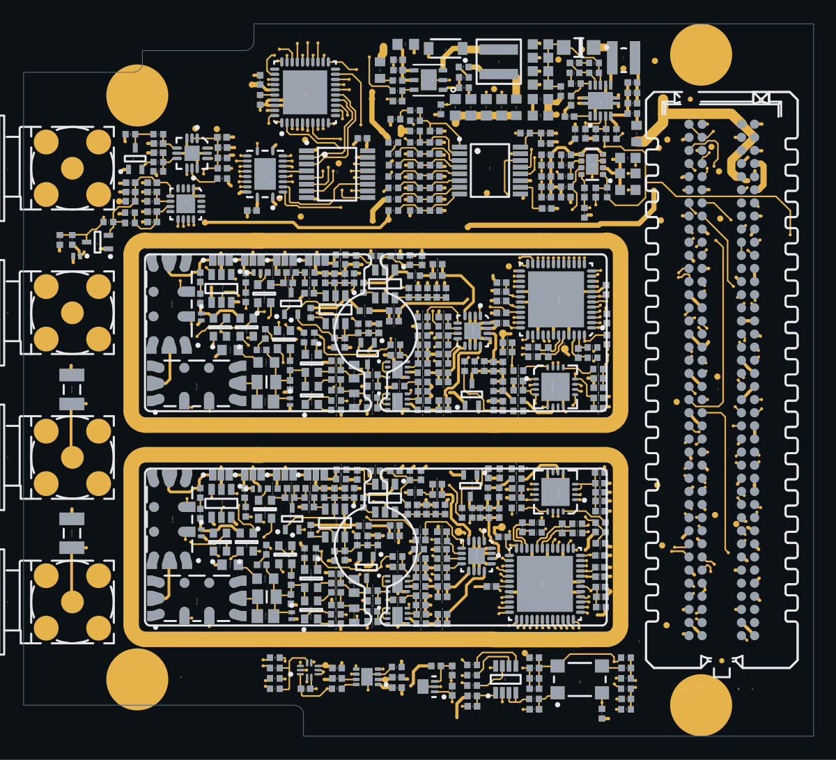
FMC ADC 1G8B2CHA (OHWR0010 R1) is an open-hardware circuit board from the CERN Open Hardware Repository, designed in Altium Designer: a 8-layer board of 76.5 × 69 mm with 1050 components and 733 nets, published under CERN-OHL-S-2.0.
review 84% walked · 26 findings: 1 blocker · 14 major · 11 minor (94 items)
Open in the interactive viewerRead the full review
Design review
Probe recorded 26 findings: 1 blocker · 14 major · 11 minor (94 items) on this design. Each is shown here with its reasoning; the full review links every one to the pins, nets and datasheet pages it rests on.
- NetCopperSplitblockerOpen
GND's copper is in 2 pieces: MSBOX1_Input1.1 and MSBOX1_Input1.2 are not connected to the rest of the net
GND's copper is in 2 pieces: MSBOX1_Input1.1 and MSBOX1_Input1.2 are not connected to the rest of the net. Piece 1: B1.1, B2.1, B3.1, B4.1, C102_Attenuator_AC1.1, C102_Attenuator_AC2.1, C103.1, C104_Attenuator_AC1.1 and 611 more pin(s), on TOP_LAYER, L2, L3, L4, L5, L6, L7 and BOTTOM_LAYER, 510 drill(s), 8992.21 mm2 of pour, over (-65, -3) to (10.25, 66). Piece 2: MSBOX1_Input1.1 and MSBOX1_Input1.2, on TOP_LAYER, over (-55.95, 5.61) to (-7.05, 25.02). The export files every one of these pins under the net, so every connectivity check passes; the copper the fab builds leaves them apart. Usually a pour island that touches only one via of its own net, or a track ending short of its copper: join the piece to the net and export again.
At split:GND
TMP1075DSG went end-of-life (Obsolete)
Vendor (DigiKey) lifecycle for TMP1075DSG (Texas Instruments's listing) changed from "Active" to "Obsolete" since this board was reviewed. Placed as IC51. A sourcing/longevity risk; consider a replacement before production.
- concernCON-001majorOpen
[eol:TMP1075DSG:Obsolete] TMP1075DSG lifecycle changed from "Active" to "Obsolete" since this board was reviewed: OHWR0010 R1 FMC ADC 1G8B2CHA. A sourcing and longevity risk. Should this be replaced before the next build?
- ReferencePlaneDiscontinuitymajorOpen
24 nets change reference between 3V3P and GND at 26 vias; 24 of them partial (fastest: ATTENDC_Attenuator_AC2_P at 100 ps 10-90 %, ASSUMED)
At 26 via(s), on 24 net(s), the signal leaves a layer referenced by one of 3V3P and GND for a layer referenced by the other, and no plane references both layers. Different nets: no via can carry the return across; only decoupling between the two planes near the via can. The capacitor carrying the return across was measured at each via, at the knee of the crossing net's edge against 50 ohm assumed: 26 with none. 26 of them at an ASSUMED edge (no edge on file for the net): state one (net_timing_state) and it is re-read. One decision covers the pair: whether 3V3P and GND are decoupled to each other near these vias. A via whose layers have more references than these two is a site of each pair it joins. 24 of them are partial: another reference continues across through a stitching via of its net, so only part of the return has nowhere to go. The pure ones are listed first, then the partial ones with the farthest stitching via first.
- 'I2CBUS.SCL' at (-18.74, 49.47), TOP_LAYER -> L6: GND on L2 to 3V3P on L5, GND on L7; partial, GND continues through a via of GND 8.71 mm away; stitching none, 29.5 mm of track past the via on L6: At the 5 GHz knee of a 100 ps edge (10 ns 10-90 %, assumed: no edge is on file for the net) no capacitor carries the return; only the planes do. 3V3P and GND are not a thin pair (at most 0.2 mm), so their own capacitance does not carry the return. To serve it, change layers across the same plane, or move the signal to a layer referenced to ground. Measured for reference: C195 (100 nF 0402) 2.5 mm away: 0.55 nH in the 0.462 mm cavity + 0.30 nH ESL + 0.81 nH mounting (pad 0.07 nH (vias beside the pads) + 1 via pair(s) at 1.57 mm pitch, 0.20 mm drill, 0.68 mm to the farther plane): 52.2 ohm at the knee, 104 % of 50 ohm (assumed track impedance). None.
- 'ATTENDC_Attenuator_AC2_P' at (-21.62, 31.19), L3 -> L6: GND on L2, 1V8P on L4 to 3V3P on L5, GND on L7; partial, GND continues through a via of GND 11.36 mm away; stitching none, 25.5 mm of track past the via on L6: At the 5 GHz knee of a 100 ps edge (100 ps 10-90 %, assumed: no edge is on file for the net) no capacitor carries the return; only the planes do. 3V3P and GND are not a thin pair (at most 0.2 mm), so their own capacitance does not carry the return. To serve it, change layers across the same plane, or move the signal to a layer referenced to ground. None.
- '3V3F_Attenuator_AC2' at (-21.56, 28.4), TOP_LAYER -> L6: GND on L2 to 3V3P on L5, GND on L7; partial, GND continues through a via of GND 13.6 mm away; stitching none, 21.0 mm of track past the via on L6: At the 5 GHz knee of a 100 ps edge (20 ns 10-90 %, assumed: no edge is on file for the net) no capacitor carries the return; only the planes do. 3V3P and GND are not a thin pair (at most 0.2 mm), so their own capacitance does not carry the return. To serve it, change layers across the same plane, or move the signal to a layer referenced to ground. None.
- 'OFFSET1_SPI.OFFSETSCLK' at (-21.97, 43.18), L3 -> L6: GND on L2, 1V8P on L4 to 3V3P on L5, GND on L7; partial, GND continues through a via of GND 6.74 mm away; stitching none, 14.6 mm of track past the via on L6: At the 5 GHz knee of a 100 ps edge (1 ns 10-90 %, assumed: no edge is on file for the net) no capacitor carries the return; only the planes do. 3V3P and GND are not a thin pair (at most 0.2 mm), so their own capacitance does not carry the return. To serve it, change layers across the same plane, or move the signal to a layer referenced to ground. None.
- 'NetC113_ADC2_2' at (-10.6, 36.57), TOP_LAYER -> L6: GND on L2 to 3V3P on L5, GND on L7; partial, GND continues through a via of GND 5.03 mm away; stitching none, 12.2 mm of track past the via on L6: At the 5 GHz knee of a 100 ps edge (100 ps 10-90 %, assumed: no edge is on file for the net) no capacitor carries the return; only the planes do. 3V3P and GND are not a thin pair (at most 0.2 mm), so their own capacitance does not carry the return. To serve it, change layers across the same plane, or move the signal to a layer referenced to ground. None.
- 'ACGAIN1_SPI.ACGAINSDIO' at (-23.39, 47.37), L3 -> L6: GND on L2, 1V8P on L4 to 3V3P on L5, GND on L7; partial, GND continues through a via of GND 9.92 mm away; stitching none, 11.5 mm of track past the via on L6: At the 5 GHz knee of a 100 ps edge (2 ns 10-90 %, assumed: no edge is on file for the net) no capacitor carries the return; only the planes do. 3V3P and GND are not a thin pair (at most 0.2 mm), so their own capacitance does not carry the return. To serve it, change layers across the same plane, or move the signal to a layer referenced to ground. None.
- 'ACGAIN1_SPI.ACGAINSDIO' at (-21.34, 43.71), L3 -> L6: GND on L2, 1V8P on L4 to 3V3P on L5, GND on L7; partial, GND continues through a via of GND 6.3 mm away; stitching none, 11.5 mm of track past the via on L6: At the 5 GHz knee of a 100 ps edge (2 ns 10-90 %, assumed: no edge is on file for the net) no capacitor carries the return; only the planes do. 3V3P and GND are not a thin pair (at most 0.2 mm), so their own capacitance does not carry the return. To serve it, change layers across the same plane, or move the signal to a layer referenced to ground. None.
- 'CH2_SELECT.V4' at (-25.7, 30.38), L3 -> L6: GND on L2, 1V8P on L4 to 3V3P on L5, GND on L7; partial, GND continues through a via of GND 14.83 mm away; stitching none, 9.8 mm of track past the via on L6: At the 5 GHz knee of a 100 ps edge (20 ns 10-90 %, assumed: no edge is on file for the net) no capacitor carries the return; only the planes do. 3V3P and GND are not a thin pair (at most 0.2 mm), so their own capacitance does not carry the return. To serve it, change layers across the same plane, or move the signal to a layer referenced to ground. None.
- 'IOEXP_SPI.IOEXPSDI' at (-19.13, 48.13), L3 -> L6: GND on L2, 1V8P on L4 to 3V3P on L5, GND on L7; partial, GND continues through a via of GND 7.66 mm away; stitching none, 5.0 mm of track past the via on L6: At the 5 GHz knee of a 100 ps edge (2 ns 10-90 %, assumed: no edge is on file for the net) no capacitor carries the return; only the planes do. 3V3P and GND are not a thin pair (at most 0.2 mm), so their own capacitance does not carry the return. To serve it, change layers across the same plane, or move the signal to a layer referenced to ground. Measured for reference: C195 (100 nF 0402) 2.3 mm away: 0.54 nH in the 0.462 mm cavity + 0.30 nH ESL + 0.81 nH mounting (pad 0.07 nH (vias beside the pads) + 1 via pair(s) at 1.57 mm pitch, 0.20 mm drill, 0.68 mm to the farther plane): 51.8 ohm at the knee, 104 % of 50 ohm (assumed track impedance). None.
- 'NetC37_Attenuator_DC2_2' at (-21.69, 41.71), L3 -> L6: GND on L2, 1V8P on L4 to 3V3P on L5, GND on L7; partial, GND continues through a via of GND 6.22 mm away; stitching none, 3.9 mm of track past the via on L6: At the 5 GHz knee of a 100 ps edge (100 ps 10-90 %, assumed: no edge is on file for the net) no capacitor carries the return; only the planes do. 3V3P and GND are not a thin pair (at most 0.2 mm), so their own capacitance does not carry the return. To serve it, change layers across the same plane, or move the signal to a layer referenced to ground. None.
- 'OFFSET1_SPI.OFFSETSDI' at (-19.3, 47.55), L3 -> L6: GND on L2, 1V8P on L4 to 3V3P on L5, GND on L7; partial, GND continues through a via of GND 7.24 mm away; stitching none, 2.1 mm of track past the via on L6: At the 5 GHz knee of a 100 ps edge (2 ns 10-90 %, assumed: no edge is on file for the net) no capacitor carries the return; only the planes do. 3V3P and GND are not a thin pair (at most 0.2 mm), so their own capacitance does not carry the return. To serve it, change layers across the same plane, or move the signal to a layer referenced to ground. Measured for reference: C195 (100 nF 0402) 2.5 mm away: 0.55 nH in the 0.462 mm cavity + 0.30 nH ESL + 0.81 nH mounting (pad 0.07 nH (vias beside the pads) + 1 via pair(s) at 1.57 mm pitch, 0.20 mm drill, 0.68 mm to the farther plane): 52.2 ohm at the knee, 104 % of 50 ohm (assumed track impedance). None.
- 'NetIC28_ADC2_6' at (-9.14, 39.12), TOP_LAYER -> L6: GND on L2 to 3V3P on L5, GND on L7; partial, GND continues through a via of GND 5.27 mm away; stitching none, 1.7 mm of track past the via on L6: At the 5 GHz knee of a 100 ps edge (100 ps 10-90 %, assumed: no edge is on file for the net) no capacitor carries the return; only the planes do. 3V3P and GND are not a thin pair (at most 0.2 mm), so their own capacitance does not carry the return. To serve it, change layers across the same plane, or move the signal to a layer referenced to ground. None.
- and 14 more
Every site is a row of this finding's evidence, keyed by net, layers and position. GET /api/odb/boards/13/reference-planes?group=refchange%3A3V3P%7CGND serves each with its own layer_image region; all of them lie in x -30.1..5.12, y 16.24..51.47 mm (board frame, Y up).
The reference on each layer is the first plane the track meets leaving the via, anti-pads and the net's own copper skipped. Whether it matters depends on each signal's edge rate, which nothing on file states for these nets: a slow static line crosses a split harmlessly, a fast edge does not.
At refchange:3V3P|GND
- PartLifecyclemajorOpen
853S01AKILF on IC35: the distributor catalogue reports "Discontinued at DigiKey" for Renesas Electronics Corporation's 853S01AKILF
853S01AKILF on IC35: the distributor catalogue reports "Discontinued at DigiKey" for Renesas Electronics Corporation's 853S01AKILF — a sourcing/longevity risk to confirm against the MANUFACTURER before acting. This board's BOM names INTEGRATED DEVICE TECHNOLOGY (IDT), and that is one line with Renesas Electronics Corporation: Renesas completed its acquisitions of Intersil on 2017-02-24, Integrated Device Technology on 2019-03-29 and Dialog Semiconductor (which had acquired Adesto Technologies in 2020) on 2021-08-31. A distributor delisting is not the same claim as the part being unavailable; check the vendor's own lifecycle/product-change notice for the status and any named successor. Re-read the source: GET /api/odb/parts/853S01AKILF/providers (which provider said it, the maker and part number it matched, its own words, and when we asked). No approved alternate is recorded for this position.
At IC35
- BomLayoutMismatchmajorOpen
BomLayoutMismatch: 3 components×3
3 checked by the review by evaluation@esharp.se — 3 different reasons
At C136, C138, D7
Each finding, with its own headline
- C136'C136' is placed in the layout but absent from the BOM.
- C138'C138' is placed in the layout but absent from the BOM.
- D7'D7' is placed in the layout but absent from the BOM.
- EsdProtectorPlacementmajorOpen
D7.1 on 'TRIGI/O': D7 joins the line 5.07 mm from J4.1 on a 5.07 mm run to R156.2
D7 (ESD351DPY) protects 'TRIGI/O' at J4.1. Along the copper: 6.07 mm of track from the contact, 0 via(s) before it, on a 1 mm branch off the line; the line runs 5.07 mm on to R156.2; D7 sits 1.61 mm farther from the contact than the nearest place outside J4.
D7 joins the line 5.07 mm from J4.1 on a 5.07 mm run to R156.2: nearer the far end than the contact, so the surge travels most of the line before it is clamped.
Measured on the copper the ODB states: tracks, the pads they land on, and the netlist's vias. Not a straight line between centroids.
At D7
- DecapViaFanoutmajorOpen
DecapViaFanout: 3 components×3
Checked by the review, stands · Claude walker W3 (Cern session) — Checked: the fan-out length is read from the copper as stated. The 0.5 nH limit is Probe's starting value, not a datasheet or vendor requirement on file; whether it matters depends on this capacitor's role in the rail's PDN target. Left for the owner.
At C161, C275, C276
Each finding, with its own headline
C161C161 on '3V3P': its rail pad reaches its via over 1.81 mm of track and its ground pad over 1.99 mm, adding about 0.70 nH to its loop, past Probe's 0.5 nH starting value; put the vias at the pads
C161 on '3V3P': its rail pad reaches its via over 1.81 mm of track and its ground pad over 1.99 mm, adding about 0.70 nH to its loop, past Probe's 0.5 nH starting value; put the vias at the pads. C161.2 (rail) runs 1.81 mm along its copper to its nearest via, 0.81 mm past the 1 mm beside the pad: 0.32 nH; C161.1 (ground) runs 1.99 mm along its copper to its nearest via, 0.99 mm past the 1 mm beside the pad: 0.39 nH. Each run past the pad as one conductor of a pair 0.90 mm apart (the pad pitch), 0.2 l ln(D/R) nH with R 0.127 mm (the track's width is not read): 0.70 nH in all. Put the vias at the pads (or in them), one per pad at least, the rail's and the ground's close together; the capacitor's own inductance as mounted is 0.50 nH (pad 0.07 nH + no via of the first net within 1 mm of its pad: the study's 0.6 nH per mm of 0.21 mm depth, ASSUMED). 0.5 nH is Probe's starting value, about the whole mounted inductance of a well-mounted 0402.
C275C275 on '11V0P': its rail pad reaches its via over 2.48 mm of track and its ground pad over 0.75 mm, adding about 0.73 nH to its loop, past Probe's 0.5 nH starting value; put the vias at the pads
C275 on '11V0P': its rail pad reaches its via over 2.48 mm of track and its ground pad over 0.75 mm, adding about 0.73 nH to its loop, past Probe's 0.5 nH starting value; put the vias at the pads. C275.2 (rail) runs 2.48 mm along its copper to its nearest via, 1.48 mm past the 1 mm beside the pad: 0.73 nH; C275.1 (ground) runs 0.75 mm along its copper to its nearest via, beside the pad. Each run past the pad as one conductor of a pair 1.50 mm apart (the pad pitch), 0.2 l ln(D/R) nH with R 0.127 mm (the track's width is not read): 0.73 nH in all. Put the vias at the pads (or in them), one per pad at least, the rail's and the ground's close together; the capacitor's own inductance as mounted is 0.74 nH (pad 0.10 nH + no via of the first net within 1 mm of its pad: the study's 0.6 nH per mm of 0.21 mm depth, ASSUMED). 0.5 nH is Probe's starting value, about the whole mounted inductance of a well-mounted 0402.
C276C276 on '11V0P': its rail pad reaches its via over 3.98 mm of track and its ground pad over 0.77 mm, adding about 1.47 nH to its loop, past Probe's 0.5 nH starting value; put the vias at the pads
C276 on '11V0P': its rail pad reaches its via over 3.98 mm of track and its ground pad over 0.77 mm, adding about 1.47 nH to its loop, past Probe's 0.5 nH starting value; put the vias at the pads. C276.2 (rail) runs 3.98 mm along its copper to its nearest via, 2.98 mm past the 1 mm beside the pad: 1.47 nH; C276.1 (ground) runs 0.77 mm along its copper to its nearest via, beside the pad. Each run past the pad as one conductor of a pair 1.50 mm apart (the pad pitch), 0.2 l ln(D/R) nH with R 0.127 mm (the track's width is not read): 1.47 nH in all. Put the vias at the pads (or in them), one per pad at least, the rail's and the ground's close together; the capacitor's own inductance as mounted is 0.74 nH (pad 0.10 nH + no via of the first net within 1 mm of its pad: the study's 0.6 nH per mm of 0.21 mm depth, ASSUMED). 0.5 nH is Probe's starting value, about the whole mounted inductance of a well-mounted 0402.
- DuplicatePassivemajorOpen
DuplicatePassive: 3 nets×3
Checked by the review, stands · Claude walker (cern session) — Stands: two fitted 200k pull-downs on each SDO net (R205+R55_Attenuator_DC1, R207+R55_Attenuator_DC2, R143+R206), one on the device sheet and one at the IC49 SN74CB3Q3251 MISO mux input (netlist), 100k effective. Electrically harmless (a weak bus-keeper on a tri-stated SDO), but the duplication is real; left for the owner.
At OFFSET1_SPI.OFFSETSDO, OFFSET2_SPI.OFFSETSDO, SYNTH_SPI.SYNTHSDO
Each finding, with its own headline
OFFSET1_SPI.OFFSETSDO'OFFSET1_SPI.OFFSETSDO' is pulled to 'GND' by 2 fitted resistors (R205 (200k), R55_Attenuator_DC1 (200k))
'OFFSET1_SPI.OFFSETSDO' is pulled to 'GND' by 2 fitted resistors: R205 (200k), R55_Attenuator_DC1 (200k) — 100k effective. A pull-up's value is specified, and two of them in parallel is not the value that was specified — presence checks are satisfied by either one and cannot see the pair. Which one is intended? Removing the duplicate, or recording that the parallel value is deliberate, both settle it; leaving two identical resistors on one node does not.
OFFSET2_SPI.OFFSETSDO'OFFSET2_SPI.OFFSETSDO' is pulled to 'GND' by 2 fitted resistors (R207 (200k), R55_Attenuator_DC2 (200k))
'OFFSET2_SPI.OFFSETSDO' is pulled to 'GND' by 2 fitted resistors: R207 (200k), R55_Attenuator_DC2 (200k) — 100k effective. A pull-up's value is specified, and two of them in parallel is not the value that was specified — presence checks are satisfied by either one and cannot see the pair. Which one is intended? Removing the duplicate, or recording that the parallel value is deliberate, both settle it; leaving two identical resistors on one node does not.
SYNTH_SPI.SYNTHSDO'SYNTH_SPI.SYNTHSDO' is pulled to 'GND' by 2 fitted resistors (R143 (200k), R206 (200k))
'SYNTH_SPI.SYNTHSDO' is pulled to 'GND' by 2 fitted resistors: R143 (200k), R206 (200k) — 100k effective. A pull-up's value is specified, and two of them in parallel is not the value that was specified — presence checks are satisfied by either one and cannot see the pair. Which one is intended? Removing the duplicate, or recording that the parallel value is deliberate, both settle it; leaving two identical resistors on one node does not.
- EsdProtectorPlacementmajorOpen
EsdProtectorPlacement: 3 components×3
e.g. “D9.1 on 'NetC179_1': D9.1 hangs 1.24 mm off the line (limit 1 mm, default” · 2 different statements
At D10, D9
Each finding, with its own headline
D10D10.1 on 'NetC184_2': 7 via(s) between C184.2 and D10.1
D10 (ESD351DPY) protects 'NetC184_2' at C184.2, where a strike from J3.1 through C184 enters the net. Along the copper: 2.29 mm of track from the contact, 7 via(s) before it, on a 1.77 mm branch off the line; the line runs 1.64 mm on to R169.2; D10 sits at C184, within 0 mm of the nearest place outside it to the contact: the track to it is mostly the escape out of C184's own pins, which no placement shortens.
7 via(s) between C184.2 and D10.1: the strike reaches an inner layer before it is clamped. D10.1 hangs 1.77 mm off the line (limit 1 mm, default: no datasheet figure on file): the line carries the strike past it while the clamp is reached through the branch.
Measured on the copper the ODB states: tracks, the pads they land on, and the netlist's vias. Not a straight line between centroids.
D9D9.1 on 'NetC179_1': D9.1 hangs 1.24 mm off the line (limit 1 mm, default
D9 (ESD351DPY) protects 'NetC179_1' at C179.1, where a strike from J3.1 through C179 enters the net. Along the copper: 1.24 mm of track from the contact, 0 via(s) before it, on a 1.24 mm branch off the line; the line runs 1.15 mm on to R297.1; D9 sits at C179, within 0.54 mm of the nearest place outside it to the contact: the track to it is mostly the escape out of C179's own pins, which no placement shortens.
D9.1 hangs 1.24 mm off the line (limit 1 mm, default: no datasheet figure on file): the line carries the strike past it while the clamp is reached through the branch.
Measured on the copper the ODB states: tracks, the pads they land on, and the netlist's vias. Not a straight line between centroids.
D9D9.1 on 'NetC179_1': D9.1 hangs 1.24 mm off the line (limit 1 mm, default
D9 (ESD351DPY) protects 'NetC179_1' at R297.1, where a strike from J3.1 through R297 enters the net. Along the copper: 2.39 mm of track from the contact, 0 via(s) before it, on a 1.24 mm branch off the line; the line runs 1.15 mm on to C179.1; D9 sits at R297, within 1.11 mm of the nearest place outside it to the contact: the track to it is mostly the escape out of R297's own pins, which no placement shortens.
No protection network is recognised at the entry: R297 (0) is in series at the entry, but 0 ohm is below the 100 ohm that limits a strike, so it is not counted as a protection network.
D9.1 hangs 1.24 mm off the line (limit 1 mm, default: no datasheet figure on file): the line carries the strike past it while the clamp is reached through the branch.
Measured on the copper the ODB states: tracks, the pads they land on, and the netlist's vias. Not a straight line between centroids.
- FiducialMissingmajorOpen
FiducialMissing: 2 boards×2
Checked by the review, stands · Claude walker (cern session) — Stands. None of the 1050 placed components is a fiducial (no FID/FTG refdes or fiducial part/package), and a schematic search for 'fiducial' returns nothing. Neither side carries a fiducial in the design data.
At bottom, top
Each finding, with its own headline
bottomThe bottom side carries 257 SMT component(s) and no fiducial was found on it
The bottom side carries 257 SMT component(s) but no fiducial was found on it — a placement machine has no optical reference to align to. Probe found no pad labelled .pad_usage=g_fiducial/l_fiducial (basis pad_usage); no single-pad, netless, undrilled component whose 0.5-3 mm round pad has a concentric solder-mask opening at least 1.5x its diameter with no other copper inside it (basis geometry); and no component whose refdes starts FID or whose part or package name contains FIDUCIAL (basis footprint-name). If your library names fiducials something Probe does not recognise, mark this benign — disposition_finding(rule='FiducialMissing', entity='bottom', status='benign', reason=…) — the name match only ever silences this check, it never asserts anything. If the side really has no fiducial, say so with status='confirmed': that answers the finding and keeps it gating release.
topThe top side carries 169 SMT component(s) and no fiducial was found on it
The top side carries 169 SMT component(s) but no fiducial was found on it — a placement machine has no optical reference to align to. Probe found no pad labelled .pad_usage=g_fiducial/l_fiducial (basis pad_usage); no single-pad, netless, undrilled component whose 0.5-3 mm round pad has a concentric solder-mask opening at least 1.5x its diameter with no other copper inside it (basis geometry); and no component whose refdes starts FID or whose part or package name contains FIDUCIAL (basis footprint-name). If your library names fiducials something Probe does not recognise, mark this benign — disposition_finding(rule='FiducialMissing', entity='top', status='benign', reason=…) — the name match only ever silences this check, it never asserts anything. If the side really has no fiducial, say so with status='confirmed': that answers the finding and keeps it gating release.
- DecapOrdermajorOpen
IC35 supply pin 13 on '3V3P': the smallest capacitor C147 sits 4.2 mm away, behind C146 at 1.2 mm
IC35 supply pin 13 on '3V3P': the smallest capacitor C147 sits 4.2 mm away, behind C146 at 1.2 mm. IC35.13: the smallest value, C147 (10 nF), is 4.2 mm from the pin and C146 (100 nF) 1.2 mm: the high-frequency part sits behind more inductance than the bulk part, which needs it least. Swap them, or bring the smallest value to the pin: it serves the fastest current and is the one the loop inductance defeats. Distances are pad centre to pin centre in the board plane. The 5 mm radius, the 10x value step and the 1 mm / 1.5x tie tolerance are Probe's starting values.
At IC35.13
- PartLifecyclemajorOpen
PartLifecycle: 3 part numbers×3
3 Obsolete · on 14 placements
At IC16_Attenuator_AC1, IC32, IC34
Each finding, with its own headline
IC16_Attenuator_AC1AQY221N2T on 12 placements (IC16_Attenuator_AC1, IC16_Attenuator_AC2, IC24_Attenuator_AC1, IC24_Attenuator_AC2, IC27_Attenuator_AC1, IC27_Attenuator_AC2, IC4_Input1, IC4_Input2, …): the distributor catalogue reports "Obsolete" for Panasonic Industry's AQY221N2T
AQY221N2T on 12 placements (IC16_Attenuator_AC1, IC16_Attenuator_AC2, IC24_Attenuator_AC1, IC24_Attenuator_AC2, IC27_Attenuator_AC1, IC27_Attenuator_AC2, IC4_Input1, IC4_Input2, …): the distributor catalogue reports "Obsolete" for Panasonic Industry's AQY221N2T — a sourcing/longevity risk to confirm against the MANUFACTURER before acting. That is the maker this board's BOM names (PANASONIC). A distributor delisting is not the same claim as the part being unavailable; check the vendor's own lifecycle/product-change notice for the status and any named successor. Re-read the source: GET /api/odb/parts/AQY221N2T/providers (which provider said it, the maker and part number it matched, its own words, and when we asked). No approved alternate is recorded for this position.
IC32LT6660KCDC-3.3 on IC32: the distributor catalogue reports "Obsolete" for Analog Devices Inc.'s LT6660KCDC-3.3
LT6660KCDC-3.3 on IC32: the distributor catalogue reports "Obsolete" for Analog Devices Inc.'s LT6660KCDC-3.3 — a sourcing/longevity risk to confirm against the MANUFACTURER before acting. That is the maker this board's BOM names (ANALOG DEVICES). A distributor delisting is not the same claim as the part being unavailable; check the vendor's own lifecycle/product-change notice for the status and any named successor. Re-read the source: GET /api/odb/parts/LT6660KCDC-3.3/providers (which provider said it, the maker and part number it matched, its own words, and when we asked). No approved alternate is recorded for this position.
IC34LTC6951IUHF#PBF on IC34: the distributor catalogue reports "Obsolete" for Analog Devices Inc.'s LTC6951IUHF#PBF
LTC6951IUHF#PBF on IC34: the distributor catalogue reports "Obsolete" for Analog Devices Inc.'s LTC6951IUHF#PBF — a sourcing/longevity risk to confirm against the MANUFACTURER before acting. That is the maker this board's BOM names (ANALOG DEVICES). A distributor delisting is not the same claim as the part being unavailable; check the vendor's own lifecycle/product-change notice for the status and any named successor. Re-read the source: GET /api/odb/parts/LTC6951IUHF#PBF/providers (which provider said it, the maker and part number it matched, its own words, and when we asked). THE LAST BUY DATE HAS PASSED (2025-01-17, 667 day(s) ago), so this is a substitution rather than a buy. The distributor reports NONE left. No approved alternate is recorded for this position.
- ReferencePlaneDiscontinuitymajorOpen
ReferencePlaneDiscontinuity: 18 boards×18
Checked by the review, stands · Claude walker W3 (Cern session) — Checked: the reference break is read from the copper as stated. Whether it matters depends on the signal's edge rate and the receiver's margin, which no datasheet or app note on file fixes for this net; the impedance step and reflection figures are Probe's model, and the thresholds are its starting values. Layout practice, not a datasheet requirement. Left for the owner.
At along@L4:11V0N|5V0N, along@L4:11V0N|NetC122_1, along@L5:11V0P|3V3P, along@L5:11V0P|5V0P_Input1, along@L5:3V3P|5V0P_Input1, along@L5:5V0P_Input1|NetC187_1 and 12 more
Each finding, with its own headline
along@L4:11V0N|5V0N5 nets run ALONG the split between the 11V0N and 5V0N planes on L4 at 5 places, the longest 2.73 mm; the impedance rises from 29 ohm to 33 ohm there at worst, 6.8 % of each edge reflected (fastest: 50R/1MN_Channel1 at 100 ps 10-90 %, ASSUMED)
On L4 the 11V0N and 5V0N planes part, and 5 nets run down the slot between them at 5 place(s), rather than across it. This is not a crossing: the return still follows the track, in the plane on its other side and in the slot's edges, so it does not detour. What changes is the track's own impedance. With the plane gone from under it on this side for that length, its field reaches further, to the slot's edges and to the next plane beyond, so its capacitance falls and its impedance rises; every edge travelling down it is partly reflected where it enters the stretch and again where it leaves, by (Z2 - Z1)/(Z2 + Z1). The longer the stretch against the edge's rise, the more of the edge sees the full step. A crossing is generally the worse fault; a mismatch is not free. Over solid plane each track is 29 ohm; along the slot 31 ohm to 33 ohm, reflecting up to 6.8 % of each edge (a method-of-moments field solve of the cross-section, one dielectric; were the slot's edges to carry none of the return, up to 39 ohm). At 1 place(s) the impedance cannot be said: the track's centreline is not over the slot. At 1 of the 5 place(s) the rise is within 10 %, the tolerance controlled impedance is commonly built to (the stackup states none); the rest exceed it or cannot be said, so the finding is a warning. One decision covers the split line's slot: whether these tracks may run down it, or should be moved over solid plane.
- '50R/1MN_Channel1' on L3 at (-39.7, 54.7), 1.34 mm, running ALONG the split for 0.95 mm, not across it, impedance not said: the track's centreline is not over the slot; other side: GND on L2, 0.071 mm from the track against 0.071 mm to L4: 50% of the return on L4
- 'DCGAIN1_SPI.DCGAINSDI' on L3 at (-27.2, 23.01), 1.39 mm, running ALONG the split for 1.08 mm, not across it, 29 ohm over solid plane, 33 ohm along it: 6.8 % of each edge reflected; other side: GND on L2, 0.071 mm from the track against 0.071 mm to L4: 50% of the return on L4
- 'OFFSET1_SPI.OFFSETSDO' on L3 at (-27.35, 19.96), 2.89 mm, running ALONG the split for 2.58 mm, not across it, 29 ohm over solid plane, 32 ohm along it: 5.1 % of each edge reflected; other side: GND on L2, 0.071 mm from the track against 0.071 mm to L4: 50% of the return on L4
- 'DCGAIN1_SPI.DCGAINCSN' on L3 at (-27.18, 17.41), 0.92 mm, running ALONG the split for 0.88 mm, not across it, 29 ohm over solid plane, 32 ohm along it: 5.1 % of each edge reflected; other side: GND on L2, 0.071 mm from the track against 0.071 mm to L4: 50% of the return on L4
- 'CH2CAL1MUB' on L3 at (-32.98, 50.74), 3.04 mm, running ALONG the split for 2.73 mm, not across it, 29 ohm over solid plane, 31 ohm along it: 4.1 % of each edge reflected; other side: GND on L2, 0.071 mm from the track against 0.071 mm to L4: 50% of the return on L4
Every site is a row of this finding's evidence, keyed by net, layers and position. GET /api/odb/boards/13/reference-planes?group=along%40L4%3A11V0N%7C5V0N serves each with its own layer_image region; all of them lie in x -41.17..-26.15, y 15.97..55.98 mm (board frame, Y up).
Read from the copper as drawn on the reference layer, along each track's centreline at exact breakpoints. The reference is the copper beside the track, never the layer's type or name. Whether it matters depends on each signal's edge rate, which nothing on file states for these nets: a slow static line crosses a split harmlessly, a fast edge does not.
along@L4:11V0N|NetC122_12 nets run ALONG the split between the 11V0N and NetC122_1 planes on L4 at 2 places, the longest 5.58 mm; the impedance rises from 29 ohm to 39 ohm there at worst, 14.5 % of each edge reflected (fastest: ADC1DATA.LCLK_P at 1 ns 10-90 %, suggested by its name)
On L4 the 11V0N and NetC122_1 planes part, and 2 nets run down the slot between them at 2 place(s), rather than across it. This is not a crossing: the return still follows the track, in the plane on its other side and in the slot's edges, so it does not detour. What changes is the track's own impedance. With the plane gone from under it on this side for that length, its field reaches further, to the slot's edges and to the next plane beyond, so its capacitance falls and its impedance rises; every edge travelling down it is partly reflected where it enters the stretch and again where it leaves, by (Z2 - Z1)/(Z2 + Z1). The longer the stretch against the edge's rise, the more of the edge sees the full step. A crossing is generally the worse fault; a mismatch is not free. Over solid plane each track is 29 ohm to 36 ohm; along the slot 39 ohm to 42 ohm, reflecting up to 14.5 % of each edge (a method-of-moments field solve of the cross-section, one dielectric; were the slot's edges to carry none of the return, up to 46 ohm). No place stays within 10 %, the tolerance controlled impedance is commonly built to (the stackup states none), so the finding is a warning. One decision covers the split line's slot: whether these tracks may run down it, or should be moved over solid plane.
- 'CAL_SPI.CALSDI' on L3 at (-2.21, 4.38), 4.71 mm, running ALONG the split for 2.77 mm, not across it, 29 ohm over solid plane, 39 ohm along it: 14.5 % of each edge reflected; other side: GND on L2, 0.071 mm from the track against 0.071 mm to L4: 50% of the return on L4
- 'ADC1DATA.LCLK_P' on L3 at (-12.28, 5.54), 5.75 mm, running ALONG the split for 5.58 mm, not across it, 36 ohm over solid plane, 42 ohm along it: 7.4 % of each edge reflected; other side: GND on L2, 0.071 mm from the track against 0.071 mm to L4: 50% of the return on L4
Every site is a row of this finding's evidence, keyed by net, layers and position. GET /api/odb/boards/13/reference-planes?group=along%40L4%3A11V0N%7CNetC122_1 serves each with its own layer_image region; all of them lie in x -16.13..1.13, y 3.38..6.6 mm (board frame, Y up).
Read from the copper as drawn on the reference layer, along each track's centreline at exact breakpoints. The reference is the copper beside the track, never the layer's type or name. Whether it matters depends on each signal's edge rate, which nothing on file states for these nets: a slow static line crosses a split harmlessly, a fast edge does not.
along@L5:11V0P|3V3P'NetIC14_Attenuator_DC1_5' runs ALONG the split between the 11V0P and 3V3P planes on L5 at 1 place, the longest 0.51 mm; the impedance there is not said (fastest: NetIC14_Attenuator_DC1_5 at 100 ps 10-90 %, ASSUMED)
On L5 the 11V0P and 3V3P planes part, and 'NetIC14_Attenuator_DC1_5' runs down the slot between them at 1 place(s), rather than across it. This is not a crossing: the return still follows the track, in the plane on its other side and in the slot's edges, so it does not detour. What changes is the track's own impedance. With the plane gone from under it on this side for that length, its field reaches further, to the slot's edges and to the next plane beyond, so its capacitance falls and its impedance rises; every edge travelling down it is partly reflected where it enters the stretch and again where it leaves, by (Z2 - Z1)/(Z2 + Z1). The longer the stretch against the edge's rise, the more of the edge sees the full step. A crossing is generally the worse fault; a mismatch is not free. At 1 place(s) the impedance cannot be said: the slot's two edges were not both read beside the track. No place stays within 10 %, the tolerance controlled impedance is commonly built to (the stackup states none), so the finding is a warning. One decision covers the split line's slot: whether these tracks may run down it, or should be moved over solid plane.
- 'NetIC14_Attenuator_DC1_5' on L6 at (-25.6, 16.49), 0.65 mm, running ALONG the split for 0.51 mm, not across it, impedance not said: the slot's two edges were not both read beside the track; other side: GND on L7, 0.071 mm from the track against 0.071 mm to L5: 50% of the return on L5
Every site is a row of this finding's evidence, keyed by net, layers and position. GET /api/odb/boards/13/reference-planes?group=along%40L5%3A11V0P%7C3V3P serves each with its own layer_image region; all of them lie in x -26.6..-24.6, y 15.16..17.81 mm (board frame, Y up).
Read from the copper as drawn on the reference layer, along each track's centreline at exact breakpoints. The reference is the copper beside the track, never the layer's type or name. Whether it matters depends on each signal's edge rate, which nothing on file states for these nets: a slow static line crosses a split harmlessly, a fast edge does not.
along@L5:11V0P|5V0P_Input14 nets run ALONG the split between the 11V0P and 5V0P_Input1 planes on L5 at 4 places, the longest 1.7 mm; the impedance rises from 17 ohm to 20 ohm there at worst, 8.6 % of each edge reflected (fastest: CLK_SEL at 1 ns 10-90 %, suggested by its name)
On L5 the 11V0P and 5V0P_Input1 planes part, and 4 nets run down the slot between them at 4 place(s), rather than across it. This is not a crossing: the return still follows the track, in the plane on its other side and in the slot's edges, so it does not detour. What changes is the track's own impedance. With the plane gone from under it on this side for that length, its field reaches further, to the slot's edges and to the next plane beyond, so its capacitance falls and its impedance rises; every edge travelling down it is partly reflected where it enters the stretch and again where it leaves, by (Z2 - Z1)/(Z2 + Z1). The longer the stretch against the edge's rise, the more of the edge sees the full step. A crossing is generally the worse fault; a mismatch is not free. Over solid plane each track is 17 ohm to 29 ohm; along the slot 20 ohm to 33 ohm, reflecting up to 8.6 % of each edge (a method-of-moments field solve of the cross-section, one dielectric; were the slot's edges to carry none of the return, up to 39 ohm). At 2 of the 4 place(s) the rise is within 10 %, the tolerance controlled impedance is commonly built to (the stackup states none); the rest exceed it or cannot be said, so the finding is a warning. One decision covers the split line's slot: whether these tracks may run down it, or should be moved over solid plane.
- '3V3F_Attenuator_AC1' on L6 at (-32.3, 9.91), 1.75 mm, running ALONG the split for 1.47 mm, not across it, 17 ohm over solid plane, 20 ohm along it: 8.6 % of each edge reflected; other side: GND on L7, 0.071 mm from the track against 0.071 mm to L5: 50% of the return on L5
- 'DCGAIN2_SPI.DCGAINSCLK' on L6 at (-30.99, 36.81), 1.88 mm, running ALONG the split for 1.7 mm, not across it, 29 ohm over solid plane, 33 ohm along it: 7.2 % of each edge reflected; other side: GND on L7, 0.071 mm from the track against 0.071 mm to L5: 50% of the return on L5
- 'CLK_SEL' on L6 at (-32.89, 36.85), 1.67 mm, running ALONG the split for 1.18 mm, not across it, 29 ohm over solid plane, 32 ohm along it: 4.6 % of each edge reflected; other side: GND on L7, 0.071 mm from the track against 0.071 mm to L5: 50% of the return on L5
- 'DCGAIN2_SPI.DCGAINCSN' on L6 at (-26.6, 36.35), 0.69 mm, running ALONG the split for 0.65 mm, not across it, 29 ohm over solid plane, 32 ohm along it: 4.4 % of each edge reflected; other side: GND on L7, 0.071 mm from the track against 0.071 mm to L5: 50% of the return on L5
Every site is a row of this finding's evidence, keyed by net, layers and position. GET /api/odb/boards/13/reference-planes?group=along%40L5%3A11V0P%7C5V0P_Input1 serves each with its own layer_image region; all of them lie in x -34.65..-25.57, y 7.98..37.88 mm (board frame, Y up).
Read from the copper as drawn on the reference layer, along each track's centreline at exact breakpoints. The reference is the copper beside the track, never the layer's type or name. Whether it matters depends on each signal's edge rate, which nothing on file states for these nets: a slow static line crosses a split harmlessly, a fast edge does not.
along@L5:3V3P|5V0P_Input1'ADC1CONTROL.SCLK' runs ALONG the split between the 3V3P and 5V0P_Input1 planes on L5 at 3 places, the longest 3.53 mm; the impedance rises from 29 ohm to 38 ohm there at worst, 13.9 % of each edge reflected (fastest: ADC1CONTROL.SCLK at 1 ns 10-90 %, suggested by its name)
On L5 the 3V3P and 5V0P_Input1 planes part, and 'ADC1CONTROL.SCLK' runs down the slot between them at 3 place(s), rather than across it. This is not a crossing: the return still follows the track, in the plane on its other side and in the slot's edges, so it does not detour. What changes is the track's own impedance. With the plane gone from under it on this side for that length, its field reaches further, to the slot's edges and to the next plane beyond, so its capacitance falls and its impedance rises; every edge travelling down it is partly reflected where it enters the stretch and again where it leaves, by (Z2 - Z1)/(Z2 + Z1). The longer the stretch against the edge's rise, the more of the edge sees the full step. A crossing is generally the worse fault; a mismatch is not free. Over solid plane each track is 29 ohm; along the slot 32 ohm to 38 ohm, reflecting up to 13.9 % of each edge (a method-of-moments field solve of the cross-section, one dielectric; were the slot's edges to carry none of the return, up to 39 ohm). No place stays within 10 %, the tolerance controlled impedance is commonly built to (the stackup states none), so the finding is a warning. One decision covers the split line's slot: whether these tracks may run down it, or should be moved over solid plane.
- 'ADC1CONTROL.SCLK' on L6 at (-8.48, 10.71), 1.89 mm, running ALONG the split for 1.18 mm, not across it, 29 ohm over solid plane, 38 ohm along it: 13.9 % of each edge reflected; other side: GND on L7, 0.071 mm from the track against 0.071 mm to L5: 50% of the return on L5
- 'ADC1CONTROL.SCLK' on L6 at (-4.74, 13.28), 4.09 mm, running ALONG the split for 3.53 mm, not across it, 29 ohm over solid plane, 37 ohm along it: 12 % of each edge reflected; other side: GND on L7, 0.071 mm from the track against 0.071 mm to L5: 50% of the return on L5
- 'ADC1CONTROL.SCLK' on L6 at (-3.05, 22.24), 1.18 mm, running ALONG the split for 0.93 mm, not across it, 29 ohm over solid plane, 32 ohm along it: 5.3 % of each edge reflected; other side: GND on L7, 0.071 mm from the track against 0.071 mm to L5: 50% of the return on L5
Every site is a row of this finding's evidence, keyed by net, layers and position. GET /api/odb/boards/13/reference-planes?group=along%40L5%3A3V3P%7C5V0P_Input1 serves each with its own layer_image region; all of them lie in x -9.7..-1.85, y 8.89..23.85 mm (board frame, Y up).
Read from the copper as drawn on the reference layer, along each track's centreline at exact breakpoints. The reference is the copper beside the track, never the layer's type or name. Whether it matters depends on each signal's edge rate, which nothing on file states for these nets: a slow static line crosses a split harmlessly, a fast edge does not.
along@L5:5V0P_Input1|NetC187_1'GA1' runs ALONG the split between the 5V0P_Input1 and NetC187_1 planes on L5 at 1 place, the longest 1.89 mm; the impedance rises from 29 ohm to 32 ohm there at worst, 5.3 % of each edge reflected (fastest: GA1 at 100 ps 10-90 %, ASSUMED)
On L5 the 5V0P_Input1 and NetC187_1 planes part, and 'GA1' runs down the slot between them at 1 place(s), rather than across it. This is not a crossing: the return still follows the track, in the plane on its other side and in the slot's edges, so it does not detour. What changes is the track's own impedance. With the plane gone from under it on this side for that length, its field reaches further, to the slot's edges and to the next plane beyond, so its capacitance falls and its impedance rises; every edge travelling down it is partly reflected where it enters the stretch and again where it leaves, by (Z2 - Z1)/(Z2 + Z1). The longer the stretch against the edge's rise, the more of the edge sees the full step. A crossing is generally the worse fault; a mismatch is not free. Over solid plane each track is 29 ohm; along the slot 32 ohm, reflecting up to 5.3 % of each edge (a method-of-moments field solve of the cross-section, one dielectric; were the slot's edges to carry none of the return, up to 39 ohm). No place stays within 10 %, the tolerance controlled impedance is commonly built to (the stackup states none), so the finding is a warning. One decision covers the split line's slot: whether these tracks may run down it, or should be moved over solid plane.
- 'GA1' on L6 at (-12.7, 52.78), 2.06 mm, running ALONG the split for 1.89 mm, not across it, 29 ohm over solid plane, 32 ohm along it: 5.3 % of each edge reflected; other side: GND on L7, 0.071 mm from the track against 0.071 mm to L5: 50% of the return on L5
Every site is a row of this finding's evidence, keyed by net, layers and position. GET /api/odb/boards/13/reference-planes?group=along%40L5%3A5V0P_Input1%7CNetC187_1 serves each with its own layer_image region; all of them lie in x -14.71..-10.7, y 51.78..53.83 mm (board frame, Y up).
Read from the copper as drawn on the reference layer, along each track's centreline at exact breakpoints. The reference is the copper beside the track, never the layer's type or name. Whether it matters depends on each signal's edge rate, which nothing on file states for these nets: a slow static line crosses a split harmlessly, a fast edge does not.
merged:-39.6,55.53|-38.1,55.32'CH1AMP1' crosses between the drills at (-38.35, 54.75) and (-38.6, 55.45), whose anti-pads run together in the GND plane on L2 (fastest: CH1AMP1 at 100 ps 10-90 %, ASSUMED)
Along 'CH1AMP1' on TOP_LAYER, the GND plane on L2 is cleared round the drills at (-38.35, 54.75) and (-38.6, 55.45), and the two clearances run together: the straight line from one drill to the other is bare all the way, and the track crosses it, over 1.51 mm of bare stretch at (-38.78, 55.28). Past one drill's anti-pad the return flows round on either side; here it cannot pass between the drills and detours round the whole merged clearance - the slot a row of pins or vias cuts in a plane. No crossing has a plane on the track's other side, so the whole return meets the break.
- 'CH1AMP1' on TOP_LAYER at (-38.78, 55.28), 1.51 mm between the drills at (-38.35, 54.75) and (-38.6, 55.45) in L2; other side: none: the signal layer is outermost
Every site is a row of this finding's evidence, keyed by net, layers and position. GET /api/odb/boards/13/reference-planes?group=merged%3A-39.6%2C55.53%7C-38.1%2C55.32 serves each with its own layer_image region; all of them lie in x -40.32..-36.87, y 54.14..56.28 mm (board frame, Y up).
Read from the copper as drawn on the reference layer, along each track's centreline at exact breakpoints. The reference is the copper beside the track, never the layer's type or name. Whether it matters depends on each signal's edge rate, which nothing on file states for these nets: a slow static line crosses a split harmlessly, a fast edge does not.
refchange:11V0N|5V0P_Input1'NetC24_Attenuator_DC1_1' changes reference between 11V0N and 5V0P_Input1 at a via, none with a reference that continues across (fastest: NetC24_Attenuator_DC1_1 at 100 ps 10-90 %, ASSUMED)
At 1 via(s), on 1 net(s), the signal leaves a layer referenced by one of 11V0N and 5V0P_Input1 for a layer referenced by the other, and no plane references both layers. Different nets: no via can carry the return across; only decoupling between the two planes near the via can. The capacitor carrying the return across was measured at each via, at the knee of the crossing net's edge against 50 ohm assumed: 1 with none. 1 of them at an ASSUMED edge (no edge on file for the net): state one (net_timing_state) and it is re-read. One decision covers the pair: whether 11V0N and 5V0P_Input1 are decoupled to each other near these vias. A via whose layers have more references than these two is a site of each pair it joins. None is partial: at every one, no reference continues across the via.
- 'NetC24_Attenuator_DC1_1' at (-26.55, 21.07), L3 -> L4: GND on L2, 11V0N on L4 to 5V0P_Input1 on L5; pure, no reference continues across; stitching none, 0.7 mm of track past the via on L4: At the 5 GHz knee of a 100 ps edge (100 ps 10-90 %, assumed: no edge is on file for the net) no capacitor carries the return; only the planes do. 11V0N and 5V0P_Input1 are not a thin pair (at most 0.2 mm), so their own capacitance does not carry the return. To serve it, change layers across the same plane, or move the signal to a layer referenced to ground. None.
Every site is a row of this finding's evidence, keyed by net, layers and position. GET /api/odb/boards/13/reference-planes?group=refchange%3A11V0N%7C5V0P_Input1 serves each with its own layer_image region; all of them lie in x -28.55..-24.55, y 19.07..23.07 mm (board frame, Y up).
The reference on each layer is the first plane the track meets leaving the via, anti-pads and the net's own copper skipped. Whether it matters depends on each signal's edge rate, which nothing on file states for these nets: a slow static line crosses a split harmlessly, a fast edge does not.
refchange:1V8P|3V3P4 nets change reference between 1V8P and 3V3P at 8 vias, none with a reference that continues across (fastest: NetC261_2 at 100 ps 10-90 %, ASSUMED)
At 8 via(s), on 4 net(s), the signal leaves a layer referenced by one of 1V8P and 3V3P for a layer referenced by the other, and no plane references both layers. Different nets: no via can carry the return across; only decoupling between the two planes near the via can. The capacitor carrying the return across was measured at each via, at the knee of the crossing net's edge against 50 ohm assumed: 8 with none. 8 of them at an ASSUMED edge (no edge on file for the net): state one (net_timing_state) and it is re-read. One decision covers the pair: whether 1V8P and 3V3P are decoupled to each other near these vias. A via whose layers have more references than these two is a site of each pair it joins. None is partial: at every one, no reference continues across the via.
- 'ADC1CLK.DP_N' at (-10.48, 13.5), L5 -> L6: 1V8P on L4 to 3V3P on L5, GND on L7; pure, no reference continues across; stitching none, 14.7 mm of track past the via on L6: At the 5 GHz knee of a 100 ps edge (1 ns 10-90 %, assumed: no edge is on file for the net) no capacitor carries the return; only the planes do. 1V8P and 3V3P are not a thin pair (at most 0.2 mm), so their own capacitance does not carry the return. To serve it, change layers across the same plane, or move the signal to a layer referenced to ground. None.
- 'ADC1CLK.DP_P' at (-10.48, 14), L5 -> L6: 1V8P on L4 to 3V3P on L5, GND on L7; pure, no reference continues across; stitching none, 14.3 mm of track past the via on L6: At the 5 GHz knee of a 100 ps edge (1 ns 10-90 %, assumed: no edge is on file for the net) no capacitor carries the return; only the planes do. 1V8P and 3V3P are not a thin pair (at most 0.2 mm), so their own capacitance does not carry the return. To serve it, change layers across the same plane, or move the signal to a layer referenced to ground. None.
- 'ADC2CLK.DP_P' at (-18.13, 37.05), L5 -> L6: 1V8P on L4 to 3V3P on L5, GND on L7; pure, no reference continues across; stitching none, 13.1 mm of track past the via on L6: At the 5 GHz knee of a 100 ps edge (1 ns 10-90 %, assumed: no edge is on file for the net) no capacitor carries the return; only the planes do. 1V8P and 3V3P are not a thin pair (at most 0.2 mm), so their own capacitance does not carry the return. To serve it, change layers across the same plane, or move the signal to a layer referenced to ground. None.
- 'ADC2CLK.DP_P' at (-17.8, 37.05), L5 -> L6: 1V8P on L4 to 3V3P on L5, GND on L7; pure, no reference continues across; stitching none, 13.1 mm of track past the via on L6: At the 5 GHz knee of a 100 ps edge (1 ns 10-90 %, assumed: no edge is on file for the net) no capacitor carries the return; only the planes do. 1V8P and 3V3P are not a thin pair (at most 0.2 mm), so their own capacitance does not carry the return. To serve it, change layers across the same plane, or move the signal to a layer referenced to ground. None.
- 'NetC261_2' at (-12.47, 47.37), L5 -> L6: 1V8P on L4 to 3V3P on L5, GND on L7; pure, no reference continues across; stitching none, 0.8 mm of track past the via on L6: At the 5 GHz knee of a 100 ps edge (100 ps 10-90 %, assumed: no edge is on file for the net) no capacitor carries the return; only the planes do. 1V8P and 3V3P are not a thin pair (at most 0.2 mm), so their own capacitance does not carry the return. To serve it, change layers across the same plane, or move the signal to a layer referenced to ground. None.
- 'ADC2CLK.DP_P' at (-17.8, 37.05), L4 -> L5: 3V3P on L5 to 1V8P on L4; pure, no reference continues across; stitching none, 0.3 mm of track past the via on L5: At the 5 GHz knee of a 100 ps edge (1 ns 10-90 %, assumed: no edge is on file for the net) no capacitor carries the return; only the planes do. 1V8P and 3V3P are not a thin pair (at most 0.2 mm), so their own capacitance does not carry the return. To serve it, change layers across the same plane, or move the signal to a layer referenced to ground. None.
- 'ADC1CLK.DP_N' at (-10.8, 13.5), L4 -> L5: 3V3P on L5 to 1V8P on L4; pure, no reference continues across; stitching none, 0.3 mm of track past the via on L5: At the 5 GHz knee of a 100 ps edge (1 ns 10-90 %, assumed: no edge is on file for the net) no capacitor carries the return; only the planes do. 1V8P and 3V3P are not a thin pair (at most 0.2 mm), so their own capacitance does not carry the return. To serve it, change layers across the same plane, or move the signal to a layer referenced to ground. None.
- 'ADC1CLK.DP_P' at (-10.8, 14), L4 -> L5: 3V3P on L5 to 1V8P on L4; pure, no reference continues across; stitching none, 0.3 mm of track past the via on L5: At the 5 GHz knee of a 100 ps edge (1 ns 10-90 %, assumed: no edge is on file for the net) no capacitor carries the return; only the planes do. 1V8P and 3V3P are not a thin pair (at most 0.2 mm), so their own capacitance does not carry the return. To serve it, change layers across the same plane, or move the signal to a layer referenced to ground. None.
Every site is a row of this finding's evidence, keyed by net, layers and position. GET /api/odb/boards/13/reference-planes?group=refchange%3A1V8P%7C3V3P serves each with its own layer_image region; all of them lie in x -20.13..-8.48, y 11.5..49.37 mm (board frame, Y up).
The reference on each layer is the first plane the track meets leaving the via, anti-pads and the net's own copper skipped. Whether it matters depends on each signal's edge rate, which nothing on file states for these nets: a slow static line crosses a split harmlessly, a fast edge does not.
refchange:1V8P|5V0P_Input1'NetC75_Attenuator_AC2_2' changes reference between 1V8P and 5V0P_Input1 at 3 vias, none with a reference that continues across (fastest: NetC75_Attenuator_AC2_2 at 100 ps 10-90 %, ASSUMED)
At 3 via(s), on 1 net(s), the signal leaves a layer referenced by one of 1V8P and 5V0P_Input1 for a layer referenced by the other, and no plane references both layers. Different nets: no via can carry the return across; only decoupling between the two planes near the via can. The capacitor carrying the return across was measured at each via, at the knee of the crossing net's edge against 50 ohm assumed: 3 with none. 3 of them at an ASSUMED edge (no edge on file for the net): state one (net_timing_state) and it is re-read. One decision covers the pair: whether 1V8P and 5V0P_Input1 are decoupled to each other near these vias. A via whose layers have more references than these two is a site of each pair it joins. None is partial: at every one, no reference continues across the via.
- 'NetC75_Attenuator_AC2_2' at (-18.33, 33.48), L5 -> L6: 1V8P on L4 to 5V0P_Input1 on L5, GND on L7; pure, no reference continues across; stitching none, 0.4 mm of track past the via on L6: At the 5 GHz knee of a 100 ps edge (100 ps 10-90 %, assumed: no edge is on file for the net) no capacitor carries the return; only the planes do. 1V8P and 5V0P_Input1 are not a thin pair (at most 0.2 mm), so their own capacitance does not carry the return. To serve it, change layers across the same plane, or move the signal to a layer referenced to ground. None.
- 'NetC75_Attenuator_AC2_2' at (-18.33, 33.17), L4 -> L5: 5V0P_Input1 on L5 to 1V8P on L4; pure, no reference continues across; stitching none, 0.3 mm of track past the via on L5: At the 5 GHz knee of a 100 ps edge (100 ps 10-90 %, assumed: no edge is on file for the net) no capacitor carries the return; only the planes do. 1V8P and 5V0P_Input1 are not a thin pair (at most 0.2 mm), so their own capacitance does not carry the return. To serve it, change layers across the same plane, or move the signal to a layer referenced to ground. None.
- 'NetC75_Attenuator_AC2_2' at (-18.33, 33.18), L4 -> L5: 5V0P_Input1 on L5 to 1V8P on L4; pure, no reference continues across; stitching none, 0.3 mm of track past the via on L5: At the 5 GHz knee of a 100 ps edge (100 ps 10-90 %, assumed: no edge is on file for the net) no capacitor carries the return; only the planes do. 1V8P and 5V0P_Input1 are not a thin pair (at most 0.2 mm), so their own capacitance does not carry the return. To serve it, change layers across the same plane, or move the signal to a layer referenced to ground. None.
Every site is a row of this finding's evidence, keyed by net, layers and position. GET /api/odb/boards/13/reference-planes?group=refchange%3A1V8P%7C5V0P_Input1 serves each with its own layer_image region; all of them lie in x -20.33..-16.33, y 31.17..35.48 mm (board frame, Y up).
The reference on each layer is the first plane the track meets leaving the via, anti-pads and the net's own copper skipped. Whether it matters depends on each signal's edge rate, which nothing on file states for these nets: a slow static line crosses a split harmlessly, a fast edge does not.
refchange:1V8P|GND15 nets change reference between 1V8P and GND at 18 vias; 11 of them partial (fastest: ATTENDC_Attenuator_AC2_P at 100 ps 10-90 %, ASSUMED)
At 18 via(s), on 15 net(s), the signal leaves a layer referenced by one of 1V8P and GND for a layer referenced by the other, and no plane references both layers. Different nets: no via can carry the return across; only decoupling between the two planes near the via can. The capacitor carrying the return across was measured at each via, at the knee of the crossing net's edge against 50 ohm assumed: 18 with none. 18 of them at an ASSUMED edge (no edge on file for the net): state one (net_timing_state) and it is re-read. One decision covers the pair: whether 1V8P and GND are decoupled to each other near these vias. A via whose layers have more references than these two is a site of each pair it joins. 11 of them are partial: another reference continues across through a stitching via of its net, so only part of the return has nowhere to go. The pure ones are listed first, then the partial ones with the farthest stitching via first.
- 'ATTENDC_Attenuator_AC2_P' at (-21.62, 31.19), L3 -> L6: GND on L2, 1V8P on L4 to 3V3P on L5, GND on L7; partial, GND continues through a via of GND 11.36 mm away; stitching none, 25.5 mm of track past the via on L6: At the 5 GHz knee of a 100 ps edge (100 ps 10-90 %, assumed: no edge is on file for the net) no capacitor carries the return; only the planes do. 1V8P and GND are not a thin pair (at most 0.2 mm), so their own capacitance does not carry the return. To serve it, change layers across the same plane, or move the signal to a layer referenced to ground. None.
- 'ADC1CLK.DP_N' at (-10.48, 13.5), L5 -> L6: 1V8P on L4 to 3V3P on L5, GND on L7; pure, no reference continues across; stitching none, 14.7 mm of track past the via on L6: At the 5 GHz knee of a 100 ps edge (1 ns 10-90 %, assumed: no edge is on file for the net) no capacitor carries the return; only the planes do. 1V8P and GND are not a thin pair (at most 0.2 mm), so their own capacitance does not carry the return. To serve it, change layers across the same plane, or move the signal to a layer referenced to ground. None.
- 'OFFSET1_SPI.OFFSETSCLK' at (-21.97, 43.18), L3 -> L6: GND on L2, 1V8P on L4 to 3V3P on L5, GND on L7; partial, GND continues through a via of GND 6.74 mm away; stitching none, 14.6 mm of track past the via on L6: At the 5 GHz knee of a 100 ps edge (1 ns 10-90 %, assumed: no edge is on file for the net) no capacitor carries the return; only the planes do. 1V8P and GND are not a thin pair (at most 0.2 mm), so their own capacitance does not carry the return. To serve it, change layers across the same plane, or move the signal to a layer referenced to ground. None.
- 'ADC1CLK.DP_P' at (-10.48, 14), L5 -> L6: 1V8P on L4 to 3V3P on L5, GND on L7; pure, no reference continues across; stitching none, 14.3 mm of track past the via on L6: At the 5 GHz knee of a 100 ps edge (1 ns 10-90 %, assumed: no edge is on file for the net) no capacitor carries the return; only the planes do. 1V8P and GND are not a thin pair (at most 0.2 mm), so their own capacitance does not carry the return. To serve it, change layers across the same plane, or move the signal to a layer referenced to ground. None.
- 'ADC2CLK.DP_P' at (-18.13, 37.05), L5 -> L6: 1V8P on L4 to 3V3P on L5, GND on L7; pure, no reference continues across; stitching none, 13.1 mm of track past the via on L6: At the 5 GHz knee of a 100 ps edge (1 ns 10-90 %, assumed: no edge is on file for the net) no capacitor carries the return; only the planes do. 1V8P and GND are not a thin pair (at most 0.2 mm), so their own capacitance does not carry the return. To serve it, change layers across the same plane, or move the signal to a layer referenced to ground. None.
- 'ADC2CLK.DP_P' at (-17.8, 37.05), L5 -> L6: 1V8P on L4 to 3V3P on L5, GND on L7; pure, no reference continues across; stitching none, 13.1 mm of track past the via on L6: At the 5 GHz knee of a 100 ps edge (1 ns 10-90 %, assumed: no edge is on file for the net) no capacitor carries the return; only the planes do. 1V8P and GND are not a thin pair (at most 0.2 mm), so their own capacitance does not carry the return. To serve it, change layers across the same plane, or move the signal to a layer referenced to ground. None.
- 'ACGAIN1_SPI.ACGAINSDIO' at (-23.39, 47.37), L3 -> L6: GND on L2, 1V8P on L4 to 3V3P on L5, GND on L7; partial, GND continues through a via of GND 9.92 mm away; stitching none, 11.5 mm of track past the via on L6: At the 5 GHz knee of a 100 ps edge (2 ns 10-90 %, assumed: no edge is on file for the net) no capacitor carries the return; only the planes do. 1V8P and GND are not a thin pair (at most 0.2 mm), so their own capacitance does not carry the return. To serve it, change layers across the same plane, or move the signal to a layer referenced to ground. None.
- 'ACGAIN1_SPI.ACGAINSDIO' at (-21.34, 43.71), L3 -> L6: GND on L2, 1V8P on L4 to 3V3P on L5, GND on L7; partial, GND continues through a via of GND 6.3 mm away; stitching none, 11.5 mm of track past the via on L6: At the 5 GHz knee of a 100 ps edge (2 ns 10-90 %, assumed: no edge is on file for the net) no capacitor carries the return; only the planes do. 1V8P and GND are not a thin pair (at most 0.2 mm), so their own capacitance does not carry the return. To serve it, change layers across the same plane, or move the signal to a layer referenced to ground. None.
- 'CH2_SELECT.V4' at (-25.7, 30.38), L3 -> L6: GND on L2, 1V8P on L4 to 3V3P on L5, GND on L7; partial, GND continues through a via of GND 14.83 mm away; stitching none, 9.8 mm of track past the via on L6: At the 5 GHz knee of a 100 ps edge (20 ns 10-90 %, assumed: no edge is on file for the net) no capacitor carries the return; only the planes do. 1V8P and GND are not a thin pair (at most 0.2 mm), so their own capacitance does not carry the return. To serve it, change layers across the same plane, or move the signal to a layer referenced to ground. None.
- 'IOEXP_SPI.IOEXPSDI' at (-19.13, 48.13), L3 -> L6: GND on L2, 1V8P on L4 to 3V3P on L5, GND on L7; partial, GND continues through a via of GND 7.66 mm away; stitching none, 5.0 mm of track past the via on L6: At the 5 GHz knee of a 100 ps edge (2 ns 10-90 %, assumed: no edge is on file for the net) no capacitor carries the return; only the planes do. 1V8P and GND are not a thin pair (at most 0.2 mm), so their own capacitance does not carry the return. To serve it, change layers across the same plane, or move the signal to a layer referenced to ground. None.
- 'NetC37_Attenuator_DC2_2' at (-21.69, 41.71), L3 -> L6: GND on L2, 1V8P on L4 to 3V3P on L5, GND on L7; partial, GND continues through a via of GND 6.22 mm away; stitching none, 3.9 mm of track past the via on L6: At the 5 GHz knee of a 100 ps edge (100 ps 10-90 %, assumed: no edge is on file for the net) no capacitor carries the return; only the planes do. 1V8P and GND are not a thin pair (at most 0.2 mm), so their own capacitance does not carry the return. To serve it, change layers across the same plane, or move the signal to a layer referenced to ground. None.
- 'OFFSET1_SPI.OFFSETSDO' at (-23.83, 37.5), L3 -> L6: GND on L2, 1V8P on L4 to 5V0P_Input1 on L5, GND on L7; partial, GND continues through a via of GND 9.22 mm away; stitching none, 2.5 mm of track past the via on L6: At the 5 GHz knee of a 100 ps edge (2 ns 10-90 %, assumed: no edge is on file for the net) no capacitor carries the return; only the planes do. 1V8P and GND are not a thin pair (at most 0.2 mm), so their own capacitance does not carry the return. To serve it, change layers across the same plane, or move the signal to a layer referenced to ground. None.
- and 6 more
Every site is a row of this finding's evidence, keyed by net, layers and position. GET /api/odb/boards/13/reference-planes?group=refchange%3A1V8P%7CGND serves each with its own layer_image region; all of them lie in x -27.7..-8.48, y 11.5..50.13 mm (board frame, Y up).
The reference on each layer is the first plane the track meets leaving the via, anti-pads and the net's own copper skipped. Whether it matters depends on each signal's edge rate, which nothing on file states for these nets: a slow static line crosses a split harmlessly, a fast edge does not.
refchange:1V8P|NetC187_1'NetC261_2' changes reference between 1V8P and NetC187_1 at 2 vias, none with a reference that continues across (fastest: NetC261_2 at 100 ps 10-90 %, ASSUMED)
At 2 via(s), on 1 net(s), the signal leaves a layer referenced by one of 1V8P and NetC187_1 for a layer referenced by the other, and no plane references both layers. Different nets: no via can carry the return across; only decoupling between the two planes near the via can. The capacitor carrying the return across was measured at each via, at the knee of the crossing net's edge against 50 ohm assumed: 2 with none. 2 of them at an ASSUMED edge (no edge on file for the net): state one (net_timing_state) and it is re-read. One decision covers the pair: whether 1V8P and NetC187_1 are decoupled to each other near these vias. A via whose layers have more references than these two is a site of each pair it joins. None is partial: at every one, no reference continues across the via.
- 'NetC261_2' at (-12.47, 47.69), L4 -> L5: NetC187_1 on L5 to 1V8P on L4; pure, no reference continues across; stitching none, 0.3 mm of track past the via on L5: At the 5 GHz knee of a 100 ps edge (100 ps 10-90 %, assumed: no edge is on file for the net) no capacitor carries the return; only the planes do. 1V8P and NetC187_1 are not a thin pair (at most 0.2 mm), so their own capacitance does not carry the return. To serve it, change layers across the same plane, or move the signal to a layer referenced to ground. None.
- 'NetC261_2' at (-12.47, 47.68), L4 -> L5: NetC187_1 on L5 to 1V8P on L4; pure, no reference continues across; stitching none, 0.3 mm of track past the via on L5: At the 5 GHz knee of a 100 ps edge (100 ps 10-90 %, assumed: no edge is on file for the net) no capacitor carries the return; only the planes do. 1V8P and NetC187_1 are not a thin pair (at most 0.2 mm), so their own capacitance does not carry the return. To serve it, change layers across the same plane, or move the signal to a layer referenced to ground. None.
Every site is a row of this finding's evidence, keyed by net, layers and position. GET /api/odb/boards/13/reference-planes?group=refchange%3A1V8P%7CNetC187_1 serves each with its own layer_image region; all of them lie in x -14.47..-10.47, y 45.68..49.69 mm (board frame, Y up).
The reference on each layer is the first plane the track meets leaving the via, anti-pads and the net's own copper skipped. Whether it matters depends on each signal's edge rate, which nothing on file states for these nets: a slow static line crosses a split harmlessly, a fast edge does not.
refchange:5V0P_Input1|GND31 nets change reference between 5V0P_Input1 and GND at 36 vias; 33 of them partial (fastest: 50R/1MN_Channel2 at 100 ps 10-90 %, ASSUMED)
At 36 via(s), on 31 net(s), the signal leaves a layer referenced by one of 5V0P_Input1 and GND for a layer referenced by the other, and no plane references both layers. Different nets: no via can carry the return across; only decoupling between the two planes near the via can. The capacitor carrying the return across was measured at each via, at the knee of the crossing net's edge against 50 ohm assumed: 36 with none. 36 of them at an ASSUMED edge (no edge on file for the net): state one (net_timing_state) and it is re-read. One decision covers the pair: whether 5V0P_Input1 and GND are decoupled to each other near these vias. A via whose layers have more references than these two is a site of each pair it joins. 33 of them are partial: another reference continues across through a stitching via of its net, so only part of the return has nowhere to go. The pure ones are listed first, then the partial ones with the farthest stitching via first.
- 'CLKIN_P' at (-50.67, 46.38), TOP_LAYER -> L6: GND on L2 to 5V0P_Input1 on L5, GND on L7; partial, GND continues through a via of GND 35.55 mm away; stitching none, 92.7 mm of track past the via on L6: At the 5 GHz knee of a 100 ps edge (1 ns 10-90 %, assumed: no edge is on file for the net) no capacitor carries the return; only the planes do. 5V0P_Input1 and GND are not a thin pair (at most 0.2 mm), so their own capacitance does not carry the return. To serve it, change layers across the same plane, or move the signal to a layer referenced to ground. None.
- 'CLKIN_N' at (-50.13, 46.38), TOP_LAYER -> L6: GND on L2 to 5V0P_Input1 on L5, GND on L7; partial, GND continues through a via of GND 35.01 mm away; stitching none, 91.8 mm of track past the via on L6: At the 5 GHz knee of a 100 ps edge (1 ns 10-90 %, assumed: no edge is on file for the net) no capacitor carries the return; only the planes do. 5V0P_Input1 and GND are not a thin pair (at most 0.2 mm), so their own capacitance does not carry the return. To serve it, change layers across the same plane, or move the signal to a layer referenced to ground. None.
- 'CH1_SELECT.V1' at (-44.61, 50.21), TOP_LAYER -> L6: GND on L2 to 5V0P_Input1 on L5, GND on L7; partial, GND continues through a via of GND 30.44 mm away; stitching none, 64.5 mm of track past the via on L6: At the 5 GHz knee of a 100 ps edge (20 ns 10-90 %, assumed: no edge is on file for the net) no capacitor carries the return; only the planes do. 5V0P_Input1 and GND are not a thin pair (at most 0.2 mm), so their own capacitance does not carry the return. To serve it, change layers across the same plane, or move the signal to a layer referenced to ground. Measured for reference: C285 (100 nF 0402) 2.6 mm away: 0.56 nH in the 0.462 mm cavity + 0.30 nH ESL + 0.68 nH mounting (pad 0.07 nH (vias beside the pads) + 1 via pair(s) at 1.34 mm pitch, 0.15 mm drill, 0.53 mm to the farther plane): 48.4 ohm at the knee, 97 % of 50 ohm (assumed track impedance). None.
- 'TRIP1N' at (-47.4, 20.12), L3 -> L6: GND on L2, 5V0N on L4 to 5V0P_Input1 on L5, GND on L7; partial, GND continues through a via of GND 31.44 mm away; stitching none, 15.8 mm of track past the via on L6: At the 5 GHz knee of a 100 ps edge (100 ps 10-90 %, assumed: no edge is on file for the net) no capacitor carries the return; only the planes do. 5V0P_Input1 and GND are not a thin pair (at most 0.2 mm), so their own capacitance does not carry the return. To serve it, change layers across the same plane, or move the signal to a layer referenced to ground. None.
- 'CH2_SELECT.V1' at (-32.25, 39.25), L3 -> L6: GND on L2, 11V0N on L4 to 5V0P_Input1 on L5, GND on L7; partial, GND continues through a via of GND 16.91 mm away; stitching none, 15.2 mm of track past the via on L6: At the 5 GHz knee of a 100 ps edge (20 ns 10-90 %, assumed: no edge is on file for the net) no capacitor carries the return; only the planes do. 5V0P_Input1 and GND are not a thin pair (at most 0.2 mm), so their own capacitance does not carry the return. To serve it, change layers across the same plane, or move the signal to a layer referenced to ground. None.
- 'CH2_SELECT.V1' at (-44.75, 38.23), L3 -> L6: GND on L2, 5V0N on L4 to 5V0P_Input1 on L5, GND on L7; partial, GND continues through a via of GND 29.45 mm away; stitching none, 15.2 mm of track past the via on L6: At the 5 GHz knee of a 100 ps edge (20 ns 10-90 %, assumed: no edge is on file for the net) no capacitor carries the return; only the planes do. 5V0P_Input1 and GND are not a thin pair (at most 0.2 mm), so their own capacitance does not carry the return. To serve it, change layers across the same plane, or move the signal to a layer referenced to ground. Measured for reference: C6_Input2 (100 nF 0402) 1.3 mm away: 0.43 nH in the 0.462 mm cavity + 0.30 nH ESL + 0.76 nH mounting (pad 0.07 nH (vias beside the pads) + 1 via pair(s) at 0.98 mm pitch, 0.15 mm drill, 0.68 mm to the farther plane): 46.8 ohm at the knee, 94 % of 50 ohm (assumed track impedance). None.
- 'NetC16_Input2_2' at (-40.47, 33.19), TOP_LAYER -> L6: GND on L2 to 5V0P_Input1 on L5, GND on L7; partial, GND continues through a via of GND 26.32 mm away; stitching none, 13.2 mm of track past the via on L6: At the 5 GHz knee of a 100 ps edge (100 ps 10-90 %, assumed: no edge is on file for the net) no capacitor carries the return; only the planes do. 5V0P_Input1 and GND are not a thin pair (at most 0.2 mm), so their own capacitance does not carry the return. To serve it, change layers across the same plane, or move the signal to a layer referenced to ground. None.
- 'CALCLK' at (-4.95, 3.13), L3 -> L6: GND on L2, NetC122_1 on L4 to 5V0P_Input1 on L5; pure, no reference continues across; stitching none, 8.0 mm of track past the via on L6: At the 5 GHz knee of a 100 ps edge (1 ns 10-90 %, assumed: no edge is on file for the net) no capacitor carries the return; only the planes do. 5V0P_Input1 and GND are not a thin pair (at most 0.2 mm), so their own capacitance does not carry the return. To serve it, change layers across the same plane, or move the signal to a layer referenced to ground. None.
- 'CALCLK' at (-4.72, 3.35), L3 -> L6: GND on L2, NetC122_1 on L4 to 5V0P_Input1 on L5; pure, no reference continues across; stitching none, 8.0 mm of track past the via on L6: At the 5 GHz knee of a 100 ps edge (1 ns 10-90 %, assumed: no edge is on file for the net) no capacitor carries the return; only the planes do. 5V0P_Input1 and GND are not a thin pair (at most 0.2 mm), so their own capacitance does not carry the return. To serve it, change layers across the same plane, or move the signal to a layer referenced to ground. None.
- 'NetIC9_Attenuator_DC1_1' at (-41.78, 21.64), L3 -> L6: GND on L2, 11V0N on L4 to 5V0P_Input1 on L5, GND on L7; partial, GND continues through a via of GND 26.6 mm away; stitching none, 6.4 mm of track past the via on L6: At the 5 GHz knee of a 100 ps edge (100 ps 10-90 %, assumed: no edge is on file for the net) no capacitor carries the return; only the planes do. 5V0P_Input1 and GND are not a thin pair (at most 0.2 mm), so their own capacitance does not carry the return. To serve it, change layers across the same plane, or move the signal to a layer referenced to ground. None.
- 'TRIP2N' at (-47.92, 42.4), L3 -> L6: GND on L2, 5V0N on L4 to 5V0P_Input1 on L5, GND on L7; partial, GND continues through a via of GND 32.47 mm away; stitching none, 4.5 mm of track past the via on L6: At the 5 GHz knee of a 100 ps edge (100 ps 10-90 %, assumed: no edge is on file for the net) no capacitor carries the return; only the planes do. 5V0P_Input1 and GND are not a thin pair (at most 0.2 mm), so their own capacitance does not carry the return. To serve it, change layers across the same plane, or move the signal to a layer referenced to ground. None.
- 'NetL8_Input1_2' at (-41.68, 15.19), TOP_LAYER -> L6: GND on L2 to 5V0P_Input1 on L5, GND on L7; partial, GND continues through a via of GND 24.76 mm away; stitching none, 4.2 mm of track past the via on L6: At the 5 GHz knee of a 100 ps edge (100 ps 10-90 %, assumed: no edge is on file for the net) no capacitor carries the return; only the planes do. 5V0P_Input1 and GND are not a thin pair (at most 0.2 mm), so their own capacitance does not carry the return. To serve it, change layers across the same plane, or move the signal to a layer referenced to ground. None.
- and 24 more
Every site is a row of this finding's evidence, keyed by net, layers and position. GET /api/odb/boards/13/reference-planes?group=refchange%3A5V0P_Input1%7CGND serves each with its own layer_image region; all of them lie in x -52.67..-2.72, y 1.13..52.21 mm (board frame, Y up).
The reference on each layer is the first plane the track meets leaving the via, anti-pads and the net's own copper skipped. Whether it matters depends on each signal's edge rate, which nothing on file states for these nets: a slow static line crosses a split harmlessly, a fast edge does not.
refchange:5V0P_Input1|NetC122_1'CALCLK' changes reference between 5V0P_Input1 and NetC122_1 at 2 vias, none with a reference that continues across (fastest: CALCLK at 1 ns 10-90 %, suggested by its name)
At 2 via(s), on 1 net(s), the signal leaves a layer referenced by one of 5V0P_Input1 and NetC122_1 for a layer referenced by the other, and no plane references both layers. Different nets: no via can carry the return across; only decoupling between the two planes near the via can. The capacitor carrying the return across was measured at each via, at the knee of the crossing net's edge against 50 ohm assumed: 2 with none. 2 of them at an ASSUMED edge (no edge on file for the net): state one (net_timing_state) and it is re-read. One decision covers the pair: whether 5V0P_Input1 and NetC122_1 are decoupled to each other near these vias. A via whose layers have more references than these two is a site of each pair it joins. None is partial: at every one, no reference continues across the via.
- 'CALCLK' at (-4.95, 3.13), L3 -> L6: GND on L2, NetC122_1 on L4 to 5V0P_Input1 on L5; pure, no reference continues across; stitching none, 8.0 mm of track past the via on L6: At the 5 GHz knee of a 100 ps edge (1 ns 10-90 %, assumed: no edge is on file for the net) no capacitor carries the return; only the planes do. 5V0P_Input1 and NetC122_1 are not a thin pair (at most 0.2 mm), so their own capacitance does not carry the return. To serve it, change layers across the same plane, or move the signal to a layer referenced to ground. None.
- 'CALCLK' at (-4.72, 3.35), L3 -> L6: GND on L2, NetC122_1 on L4 to 5V0P_Input1 on L5; pure, no reference continues across; stitching none, 8.0 mm of track past the via on L6: At the 5 GHz knee of a 100 ps edge (1 ns 10-90 %, assumed: no edge is on file for the net) no capacitor carries the return; only the planes do. 5V0P_Input1 and NetC122_1 are not a thin pair (at most 0.2 mm), so their own capacitance does not carry the return. To serve it, change layers across the same plane, or move the signal to a layer referenced to ground. None.
Every site is a row of this finding's evidence, keyed by net, layers and position. GET /api/odb/boards/13/reference-planes?group=refchange%3A5V0P_Input1%7CNetC122_1 serves each with its own layer_image region; all of them lie in x -6.95..-2.72, y 1.13..5.35 mm (board frame, Y up).
The reference on each layer is the first plane the track meets leaving the via, anti-pads and the net's own copper skipped. Whether it matters depends on each signal's edge rate, which nothing on file states for these nets: a slow static line crosses a split harmlessly, a fast edge does not.
split@L5:3V3P|5V0P_Input148 nets cross the split between the 3V3P and 5V0P_Input1 planes on L5 at 94 places; 93 with a plane on the track's other side (fastest: ADC1CONTROL.PD at 100 ps 10-90 %, ASSUMED)
On L5 the 3V3P and 5V0P_Input1 planes part, and 48 nets cross from one to the other at 94 place(s). The return current cannot follow a track across; it detours to wherever the two planes are joined (a stitching capacitor, or the source), and the loop it opens radiates and couples. One decision covers the boundary: whether it is stitched near these crossings, or the nets crossing it are slow enough not to care. Tracks that run ALONG this split, down the slot rather than across it, are a finding of their own: theirs is an impedance step, not a detour. At 93 of the 94 crossing(s) the track's other neighbour carries a plane, which the return can use there. 93 of the 94 crossing(s) have a plane on the track's other side at most twice as far away as the broken one (to first order each plane beside a stripline carries a share of the return inversely proportional to its distance from the track). The rest leave most or all of the return to the break, so the finding is a warning.
- 'OFFSET2_SPI.OFFSETSDO' on L6 at (-28.55, 44.4), 0.4 mm; other side: no plane on L7
- '3V3F_Attenuator_AC1' on L6 at (-29.89, 7.73), 0.27 mm; other side: GND on L7, 0.071 mm from the track against 0.071 mm to L5: 50% of the return on L5
- 'ACGAIN2_SPI.ACGAINSDIO' on L6 at (-26.02, 50.07), 0.21 mm; other side: GND on L7, 0.071 mm from the track against 0.071 mm to L5: 50% of the return on L5
- 'ACGAIN2_SPI.ACGAINSDIO' on L6 at (-23.95, 44.4), 0.4 mm; other side: GND on L7, 0.071 mm from the track against 0.071 mm to L5: 50% of the return on L5
- 'ACGAIN2_SPI.ACGAINSDIO' on L6 at (-22.85, 41.8), 0.42 mm; other side: GND on L7, 0.071 mm from the track against 0.071 mm to L5: 50% of the return on L5
- 'ADC1CONTROL.PD' on L6 at (-4.95, 22.77), 0.21 mm; other side: GND on L7, 0.071 mm from the track against 0.071 mm to L5: 50% of the return on L5
- 'ADC1CONTROL.PD' on L6 at (-2.95, 24.38), 0.21 mm; other side: GND on L7, 0.071 mm from the track against 0.071 mm to L5: 50% of the return on L5
- 'ADC1CONTROL.SDATA' on L6 at (-8.45, 9.73), 0.71 mm; other side: GND on L7, 0.071 mm from the track against 0.071 mm to L5: 50% of the return on L5
- 'ADC1CONTROL.SDATA' on L6 at (-2.75, 21.74), 0.15 mm; other side: GND on L7, 0.071 mm from the track against 0.071 mm to L5: 50% of the return on L5
- 'ADC1CONTROL.SDATA' on L6 at (-2.64, 13.2), 0.57 mm; other side: GND on L7, 0.071 mm from the track against 0.071 mm to L5: 50% of the return on L5
- 'ADC1CONTROL.SDATA' on L6 at (1.33, 24.38), 0.15 mm; other side: GND on L7, 0.071 mm from the track against 0.071 mm to L5: 50% of the return on L5
- 'ADC1DATA.D1A_N' on L6 at (-8.4, 12.92), 1.03 mm; other side: GND on L7, 0.071 mm from the track against 0.071 mm to L5: 50% of the return on L5
- and 82 more
Every site is a row of this finding's evidence, keyed by net, layers and position. GET /api/odb/boards/13/reference-planes?group=split%40L5%3A3V3P%7C5V0P_Input1 serves each with its own layer_image region; all of them lie in x -52.12..10.78, y 3.95..57.4 mm (board frame, Y up).
Read from the copper as drawn on the reference layer, along each track's centreline at exact breakpoints. The reference is the copper beside the track, never the layer's type or name. Whether it matters depends on each signal's edge rate, which nothing on file states for these nets: a slow static line crosses a split harmlessly, a fast edge does not.
void:GND@L2:hole -24.77,19.63|-24.18,20.55'NetC65_Attenuator_AC1_2' crosses one void in the GND plane on L2 at 1 place, the longest 0.5 mm; 1 over tracks of other nets routed inside it (fastest: NetC65_Attenuator_AC1_2 at 100 ps 10-90 %, ASSUMED)
Along 'NetC65_Attenuator_AC1_2' on TOP_LAYER, the GND plane on L2 has 0.5 mm under the track with copper of 5V0P_Input1, not a plane, at (-24.34, 20.4), the same plane on both sides. No single drill's anti-pad and no landing explains it: a clearance is excused only when it holds a drill and is drawn round it, or the track ends in it on the net's own pad or via, or runs through its own via's clearance and no farther. The return current detours round the void. 1 of the crossings pass over tracks of other nets routed inside the hole on the reference layer: the plane is absent there, and those tracks stand in it. What cleared it: the hole at x -24.77..-24.18, y 19.63..20.55. One decision covers the void: whether these tracks may cross it, or the plane should be filled under them. No crossing has a plane on the track's other side, so the whole return meets the break.
- 'NetC65_Attenuator_AC1_2' on TOP_LAYER at (-24.34, 20.4), 0.5 mm over copper of 5V0P_Input1, not a plane; other side: none: the signal layer is outermost
Every site is a row of this finding's evidence, keyed by net, layers and position. GET /api/odb/boards/13/reference-planes?group=void%3AGND%40L2%3Ahole%20-24.77%2C19.63%7C-24.18%2C20.55 serves each with its own layer_image region; all of them lie in x -25.72..-23.23, y 19.4..21.4 mm (board frame, Y up).
Read from the copper as drawn on the reference layer, along each track's centreline at exact breakpoints. The reference is the copper beside the track, never the layer's type or name. Whether it matters depends on each signal's edge rate, which nothing on file states for these nets: a slow static line crosses a split harmlessly, a fast edge does not.
void:GND@L7:hole -25.5,16.1|-24.9,17.04'ATTENDC_Attenuator_AC1_P' crosses one void in the GND plane on L7 at 1 place, the longest 0.55 mm; 1 over tracks of other nets routed inside it (fastest: ATTENDC_Attenuator_AC1_P at 100 ps 10-90 %, ASSUMED)
Along 'ATTENDC_Attenuator_AC1_P' on BOTTOM_LAYER, the GND plane on L7 has 0.55 mm under the track with copper of 3V3P, not a plane, at (-25.2, 16.85), the same plane on both sides. No single drill's anti-pad and no landing explains it: a clearance is excused only when it holds a drill and is drawn round it, or the track ends in it on the net's own pad or via, or runs through its own via's clearance and no farther. The return current detours round the void. 1 of the crossings pass over tracks of other nets routed inside the hole on the reference layer: the plane is absent there, and those tracks stand in it. What cleared it: the hole at x -25.5..-24.9, y 16.1..17.04. One decision covers the void: whether these tracks may cross it, or the plane should be filled under them. No crossing has a plane on the track's other side, so the whole return meets the break.
- 'ATTENDC_Attenuator_AC1_P' on BOTTOM_LAYER at (-25.2, 16.85), 0.55 mm over copper of 3V3P, not a plane; other side: none: the signal layer is outermost
Every site is a row of this finding's evidence, keyed by net, layers and position. GET /api/odb/boards/13/reference-planes?group=void%3AGND%40L7%3Ahole%20-25.5%2C16.1%7C-24.9%2C17.04 serves each with its own layer_image region; all of them lie in x -26.48..-23.92, y 15.85..17.85 mm (board frame, Y up).
Read from the copper as drawn on the reference layer, along each track's centreline at exact breakpoints. The reference is the copper beside the track, never the layer's type or name. Whether it matters depends on each signal's edge rate, which nothing on file states for these nets: a slow static line crosses a split harmlessly, a fast edge does not.
void:GND@L7:hole -7.07,29.41|-4.98,30.31'NetIC34_17' crosses one void in the GND plane on L7 at 1 place, the longest 0.58 mm; 1 over tracks of other nets routed inside it (fastest: NetIC34_17 at 100 ps 10-90 %, ASSUMED)
Along 'NetIC34_17' on BOTTOM_LAYER, the GND plane on L7 has 0.58 mm under the track with copper of 3V3P, not a plane, at (-5.23, 30), the same plane on both sides. No single drill's anti-pad and no landing explains it: a clearance is excused only when it holds a drill and is drawn round it, or the track ends in it on the net's own pad or via, or runs through its own via's clearance and no farther. The return current detours round the void. 1 of the crossings pass over tracks of other nets routed inside the hole on the reference layer: the plane is absent there, and those tracks stand in it. What cleared it: the hole at x -7.07..-4.98, y 29.41..30.31. One decision covers the void: whether these tracks may cross it, or the plane should be filled under them. No crossing has a plane on the track's other side, so the whole return meets the break.
- 'NetIC34_17' on BOTTOM_LAYER at (-5.23, 30), 0.58 mm over copper of 3V3P, not a plane; other side: none: the signal layer is outermost
Every site is a row of this finding's evidence, keyed by net, layers and position. GET /api/odb/boards/13/reference-planes?group=void%3AGND%40L7%3Ahole%20-7.07%2C29.41%7C-4.98%2C30.31 serves each with its own layer_image region; all of them lie in x -6.23..-4.23, y 28.71..31.29 mm (board frame, Y up).
Read from the copper as drawn on the reference layer, along each track's centreline at exact breakpoints. The reference is the copper beside the track, never the layer's type or name. Whether it matters depends on each signal's edge rate, which nothing on file states for these nets: a slow static line crosses a split harmlessly, a fast edge does not.
- RegulatorCapNotAtPinmajorOpen
RegulatorCapNotAtPin: 2 pins×2
e.g. “IC56 input pin 8 on '12V0N': the nearest C_IN (C237, 4.6 mm) is on the other side of the board, and none on the regulator's side is within the datasheet's 10 mm” · 2 different statements
At IC56.8, IC59.8
Each finding, with its own headline
IC56.8IC56 input pin 8 on '12V0N': the nearest C_IN (C237, 4.6 mm) is on the other side of the board, and none on the regulator's side is within the datasheet's 10 mm
IC56 input pin 8 on '12V0N': the nearest C_IN (C237, 4.6 mm) is on the other side of the board, and none on the regulator's side is within the datasheet's 10 mm. IC56.8: C237 is 4.6 mm from the pin, within the distance, but on the top with the regulator on the bottom: its loop runs through the board's thickness and a via pair, and none sits on the regulator's side; its datasheet asks for C_IN within 10 mm (TPS7A3001DRB datasheet p23, layout_max_cin_distance). Place C_IN on the regulator's side within the stated distance, its vias at its pads; the distance is the pads' centres in the board plane, and the routed copper between them can only be longer.
IC59.8IC59 input pin 8 on '12V0N': the nearest C_IN (C237, 5.6 mm) is on the other side of the board, and none on the regulator's side is within the datasheet's 10 mm
IC59 input pin 8 on '12V0N': the nearest C_IN (C237, 5.6 mm) is on the other side of the board, and none on the regulator's side is within the datasheet's 10 mm. IC59.8: C237 is 5.6 mm from the pin, within the distance, but on the top with the regulator on the bottom: its loop runs through the board's thickness and a via pair, and none sits on the regulator's side; its datasheet asks for C_IN within 10 mm (TPS7A3001DRB datasheet p23, layout_max_cin_distance). Place C_IN on the regulator's side within the stated distance, its vias at its pads; the distance is the pads' centres in the board plane, and the routed copper between them can only be longer.
Source BOM omits three placed parts: C136, C138 (PLL loop filter) and D7 (TRIGI/O ESD)
The published BOM has no line for three placed parts: C136 and C138 in the clock PLL loop filter, and the TRIGI/O ESD diode D7.
The missing parts
All three are placed on the bottom side and drawn on the schematic, but have no row in fmc-adc-1g8b2cha-bom.csv.
Part Where Nets Schematic C136 PLL loop filter, sheet 2 GND, NetC135_2 note: 33 nF 5% (KEMET C0402C333J4RACTU) C138 PLL loop filter, sheet 2 GND, NetC137_2 note: 360 pF 5% (KEMET C0402C361J5GAC7867); drawing shows 390 pF D7 TRIGI/O line, sheet 3 TRIGI/O, GND ESD351DPY, listed alongside D9 and D10, which are on the BOM The sheet 2 note reads: 'C135 & C136 33nF 5% 0402 C0402C333J4RACTU KEMET, C138 360pF 5% 0402 C0402C361J5GAC7867 KEMET ... C138 390pF. WARNING: C135,C136,C138 MUST BE CHANGED TO THE PARTS INDICATED'.
Why it matters
A build from this BOM would leave the loop-filter capacitors and the trigger-input ESD diode unfitted, or fit whatever the assembler guesses.
- The loop filter sets the PLL bandwidth quoted on sheet 2.
- D7 is the only ESD clamp on the external trigger input.
- The note also shows the intended C138 value (360 pF) differs from the drawn value (390 pF).
TPS82150 soft-start capacitor C262 is 3.3 pF, so the 6 V rail starts in current limit
The TPS82150 IC60 soft-start capacitor C262 is 3.3 pF where TI's design example uses 3.3 nF, so the 6 V rail charges its output capacitance in current limit at every power-up.
The numbers
Quantity Value Source C262 on IC60 pin 8 (SS/TR) 3.3 pF, LibRef CC0402_3.3PF_50V_0.25PF_C0G (shared line with the RF 3.3 pF C0G parts) schematic sheet 7; BOM TI design example SS/TR 3.3 nF statement Output capacitance charged by IC60 C254-C258 (5 x 4.7 µF) plus the 6V0P bank (C259, C260) through ferrite L46: about 33 µF netlist: NetC254_2 Soft-start ramp with 3.3 pF on the order of microseconds derived Current limit 1.7 A minimum rationale What the datasheet says
- 'Using a very small capacitor or leaving the SS/TR pin floating provides fastest startup time.' (TPS82150 datasheet, p.9)
- 'Larger soft start times are recommended for higher output capacitances.' (TPS82150 datasheet, p.12)
Why it matters
Starting in current limit pulls a matching surge from FMC12V0P, the carrier 12 V rail, at every power-up. A 3.3 pF value next to a 3.3 nF reference design looks like a unit slip.
TPS82150 PG is pulled up to its own 6 V output, above the datasheet limit of a rail below 6 V
The TPS82150 IC60 power-good output is pulled up by R263 to its own 6 V output, while the datasheet requires a pull-up rail below 6 V.
Where it is
- IC60 pin 7 (PG, net NetC261_2) goes through R263 100k to NetC254_2, the IC60 output, set to 6 V by R262/R264 over R265 with VFB 0.8 V.
- The same PG node drives the TPS7A8050 IC61 enable through R261.
- TPS82150 datasheet, p.10: 'The power good output requires a pull-up resistor connecting to any voltage rail less than 6V.'
Why it matters
At 6 V nominal the pull-up rail sits on the stated limit, and any positive output tolerance takes PG above it.
Suggested fix: a pull-up to a lower rail, or a divider, keeps both PG and the IC61 enable within their ratings.
TMP300 trip outputs TRIP1N/TRIP2N are pulled up to 5 V and read by the 3.3 V MAX7301
The TMP300 trip outputs TRIP1N/TRIP2N are pulled up to 5V0P and read by the MAX7301 IC64, which runs from 3.3 V, so each expander port sits about 1.4 V above its absolute maximum in normal operation.
Where it is
``
mermaid flowchart LR P["5V0P, 5 V"] -- "R1_Input1 / R1_Input2 10k" --> N["TRIP1N / TRIP2N"] T["TMP300 IC2_Input1/2<br/>pin 3 OUT, open-drain"] --> N N --> S["TS5A3166 IC1_Input1/2<br/>pin 4 IN"] N --> M["MAX7301 IC64<br/>P29 pin 25, P30 pin 27<br/>V+ = 3V3P"]``The numbers
Quantity Value Source Pull-up rail 5V0P (5V0P_Input1), 5 V netlist: TRIP1N, TRIP2N MAX7301 supply V+ (pin 35) 3V3P, 3.3 V netlist: IC64 Absolute maximum, all other pins -0.3 V to V+ + 0.3 V MAX7301 datasheet, p.2 Port level whenever the trip is not asserted 5 V, about 1.4 V above the rating derived Clamp current into 3V3P roughly 0.14 mA per port derived MAX7301 port current rating ±30 mA rationale Why it matters
The trip is normally not asserted, so the voltage rating is exceeded continuously for as long as the board runs. The injected current is well inside the stated port current.
Suggested fix: a pull-up to 3V3P, or a divider on the MAX7301 branch, keeps both the TS5A3166 control input and the expander port within ratings.
Front-end gain and coupling controls float until firmware configures the MAX7301
The front-end gain and coupling controls float until firmware configures the MAX7301 IC64: its ports default to inputs at power-up, and several of its outputs have no board-side pull.
The MAX7301 ports 'default to logic inputs on power-up' (MAX7301 datasheet, p.5).
Which outputs have a pull
MAX7301 outputs Go to Pull CH1AMP0/1, CH2AMP0/1 SN74HCT139 IC66 select inputs, directly (e.g. CH1AMP0: IC64 pin 7 P11 to IC66 pin 14 2A) none AC/DCN_Channel1/2 ADG1436 IC9 control inputs through 1k (Channel1: R22 to pin 15) none 50R/1MN_Channel1/2 ADG1436 IC9 control inputs through 1k (Channel1: IC64 pin 5 P10, R23_Attenuator_DC1 to IC9_Attenuator_DC1 pin 6) none TRIGOE, CLKOE, TRIG50R, CLK50R trigger and clock enables 10k to GND (R298, R300, R299, R301) Why it matters
Until the carrier firmware writes the expander, the 74HCT139 decoder and the ADG1436 switches see floating CMOS inputs. That leaves the channel gain, AC/DC coupling and 50 Ω / 1 MΩ selection undefined, and floating CMOS inputs can also draw shoot-through current. The relay enables through the SN74LVTH125 buffers are held by bus-hold, but in an undefined state.
Suggested fix: pull resistors to the intended safe state, as already done for the trigger and clock enables, would define the front end from power-up.
FMC SPI select and control inputs have no board-side pull before the carrier drives them
The FMC control SPI and DAC SPI inputs, including the chip selects, have no board-side pull-up or pull-down, so they float until the carrier drives them; a floating SPICSN can enable the select decoder IC45.
Where it is
Bus Signals Enters Pulls FMC control SPI FMCCSN, FMCSCLK, FMCMOSI, FMCA0-2, FMCWRN SN74LVC8T245 IC44 none on either side DAC SPI DACCSN, DACSCLK, DACDIN SN74AVC4T245 IC29 none on either side For example:
- FMC_CON_SPI.FMCCSN connects only J5 pin h37 and IC44 pin 6 (A4)
- FMCDACSPI.DACCSN connects only J5 pin d18 and IC29 pin 6 (1A1)
- SPICSN, the IC44 output that enables the SN74LVC138 select decoder IC45, connects only IC44 pin 18 (B4) and IC45 pin 4 (G2A, active-low enable)
What the datasheets require
Part Rule Source SN74LVC8T245 inputs 'must be held at logic HIGH or LOW' SN74LVC8T245 datasheet, p.7 SN74AVC4T245 'All unused data inputs of the device must be held at V or GND for proper device operation' SN74AVC4T245 datasheet, p.7 Why it matters
Before the carrier FPGA is configured its LA pins may be high-impedance, so the translator inputs float while FMCVADJ is up, which both datasheets tell the designer to avoid. A floating SPICSN can enable the decoder and assert a device select, and a floating DACCSN can do the same for the VCXO DAC.
Suggested fix: a pull-up on each chip select (and a defined level on the address lines) makes the idle state independent of the carrier.
Schematic title blocks carry placeholders: document number EDA-?????, revision "-", checker "*"
Every schematic title block carries placeholders: document number EDA-?????-V1-0, revision
-, checker*.The same fields repeat on every sheet (e.g. Power.SchDoc, ADC.SchDoc):
- Document number: EDA-?????-V1-0
- Revision:
- - Check.by:
* - Document:
* - Sheet numbering: "x of 13", although the published PDF (OHWR fmc-adc-1g8b2cha, commit 231aada8) has 18 pages because the channel sheets repeat
Why it matters
The title block is what ties a printed or exported sheet to a released revision. With a placeholder number and no revision, a reader cannot tell which build a sheet belongs to, which matters for an open-hardware design that others will fabricate.
Top-overlay designators are about 0.08 mm tall and printed across pads, so no readable refdes survives fabrication
The top-overlay designators are about 0.08 mm tall and printed across the pads they label, so no readable refdes survives fabrication.
What was measured
Quantity Value Source Designator height, e.g. R306_Attenuator_AC2 about 55 px at 654 px/mm = 0.084 mm layer render of TOP_OVERLAY + TOP_PASTE, region x -30..-15 mm, y 20..35 mm Designator stroke near 0.01 mm same render Screen-printing resolution roughly 0.8 mm text with a 0.1 mm stroke rationale - Many designators run straight across the 0402 pads they label; the R306_Attenuator_AC2 glyphs lie over the R306 pads.
- Neighbouring designators overlap each other; the C96/C97_Attenuator_AC2 designators are superimposed.
Why it matters
These designators will be dropped or smeared by the fabricator, and silk on pads is clipped away. Assembly, rework and debugging then have no refdes on the board. Component outlines and pin-1 dots are printed at a usable size, so this is a text-size setting, not missing data.
No test points on the power rails, enables or control buses; the only four test points are unfitted front-end pads
The board has no test point on any power rail, enable or control bus: its only four test points are unfitted pads in the analog front end.
The test points that exist
All four are in the analog front end and all are marked not mounted (placement populated = false; source BOM Mounted = No):
- TP1_Attenuator_AC1, TP1_Attenuator_AC2
- TP2_ADC1, TP2_ADC2
What has none
- The eleven generated rails, for example 12V0N, 11V0N, 5V0N, 6V0P, 5V0P (5V0P_Input1), 1V8P. 12V0N, for instance, carries IC56, IC59, L44, C237, C238, R243, R247 and T3 and no test point.
- The shared regulator EN net
- PG_C2M
- The MAX7301 and SPI control lines
Why it matters
Bring-up of a board with seven regulators and a carrier-dependent enable chain needs probe access to each rail and to EN. Without it every measurement lands on a 0402 capacitor end, which is slow and risks shorting adjacent parts on a dense double-sided layout.
- DecapViaFanoutminorOpen
DecapViaFanout: 4 components×4
Checked by the review, stands · Claude walker W3 (Cern session) — Checked: the fan-out length is read from the copper as stated. The 0.5 nH limit is Probe's starting value, not a datasheet or vendor requirement on file; whether it matters depends on this capacitor's role in the rail's PDN target. Left for the owner.
At C167, C280, C281, C282
Each finding, with its own headline
C167C167 on '3V3P': its rail pad reaches its via over 1.96 mm of track and its ground pad over 1.50 mm, adding about 0.57 nH to its loop, past Probe's 0.5 nH starting value; put the vias at the pads (within a quarter of the starting value)
C167 on '3V3P': its rail pad reaches its via over 1.96 mm of track and its ground pad over 1.50 mm, adding about 0.57 nH to its loop, past Probe's 0.5 nH starting value; put the vias at the pads (within a quarter of the starting value). C167.2 (rail) runs 1.96 mm along its copper to its nearest via, 0.96 mm past the 1 mm beside the pad: 0.38 nH; C167.1 (ground) runs 1.50 mm along its copper to its nearest via, 0.50 mm past the 1 mm beside the pad: 0.20 nH. Each run past the pad as one conductor of a pair 0.90 mm apart (the pad pitch), 0.2 l ln(D/R) nH with R 0.127 mm (the track's width is not read): 0.57 nH in all. Put the vias at the pads (or in them), one per pad at least, the rail's and the ground's close together; the capacitor's own inductance as mounted is 0.50 nH (pad 0.07 nH + no via of the first net within 1 mm of its pad: the study's 0.6 nH per mm of 0.21 mm depth, ASSUMED). 0.5 nH is Probe's starting value, about the whole mounted inductance of a well-mounted 0402.
C280C280 on '1V8P': its rail pad reaches its via over 3.78 mm of track and its ground pad over 0.68 mm, adding about 1.41 nH to its loop, past Probe's 0.5 nH starting value; put the vias at the pads (a 22 uF bulk capacitor: its inductance matters only far above the band it serves)
C280 on '1V8P': its rail pad reaches its via over 3.78 mm of track and its ground pad over 0.68 mm, adding about 1.41 nH to its loop, past Probe's 0.5 nH starting value; put the vias at the pads (a 22 uF bulk capacitor: its inductance matters only far above the band it serves). C280.2 (rail) runs 3.78 mm along its copper to its nearest via, 2.78 mm past the 1 mm beside the pad: 1.41 nH; C280.1 (ground) runs 0.68 mm along its copper to its nearest via, beside the pad. Each run past the pad as one conductor of a pair 1.60 mm apart (the pad pitch), 0.2 l ln(D/R) nH with R 0.127 mm (the track's width is not read): 1.41 nH in all. Put the vias at the pads (or in them), one per pad at least, the rail's and the ground's close together; the capacitor's own inductance as mounted is 0.74 nH (pad 0.10 nH + no via of the first net within 1 mm of its pad: the study's 0.6 nH per mm of 0.21 mm depth, ASSUMED). 0.5 nH is Probe's starting value, about the whole mounted inductance of a well-mounted 0402.
C281C281 on '1V8P': its rail pad reaches its via over 5.28 mm of track and its ground pad over 0.68 mm, adding about 2.17 nH to its loop, past Probe's 0.5 nH starting value; put the vias at the pads (a 22 uF bulk capacitor: its inductance matters only far above the band it serves)
C281 on '1V8P': its rail pad reaches its via over 5.28 mm of track and its ground pad over 0.68 mm, adding about 2.17 nH to its loop, past Probe's 0.5 nH starting value; put the vias at the pads (a 22 uF bulk capacitor: its inductance matters only far above the band it serves). C281.2 (rail) runs 5.28 mm along its copper to its nearest via, 4.28 mm past the 1 mm beside the pad: 2.17 nH; C281.1 (ground) runs 0.68 mm along its copper to its nearest via, beside the pad. Each run past the pad as one conductor of a pair 1.60 mm apart (the pad pitch), 0.2 l ln(D/R) nH with R 0.127 mm (the track's width is not read): 2.17 nH in all. Put the vias at the pads (or in them), one per pad at least, the rail's and the ground's close together; the capacitor's own inductance as mounted is 0.74 nH (pad 0.10 nH + no via of the first net within 1 mm of its pad: the study's 0.6 nH per mm of 0.21 mm depth, ASSUMED). 0.5 nH is Probe's starting value, about the whole mounted inductance of a well-mounted 0402.
C282C282 on '1V8P': its rail pad reaches its via over 2.28 mm of track and its ground pad over 0.00 mm, adding about 0.65 nH to its loop, past Probe's 0.5 nH starting value; put the vias at the pads (a 22 uF bulk capacitor: its inductance matters only far above the band it serves)
C282 on '1V8P': its rail pad reaches its via over 2.28 mm of track and its ground pad over 0.00 mm, adding about 0.65 nH to its loop, past Probe's 0.5 nH starting value; put the vias at the pads (a 22 uF bulk capacitor: its inductance matters only far above the band it serves). C282.2 (rail) runs 2.28 mm along its copper to its nearest via, 1.28 mm past the 1 mm beside the pad: 0.65 nH; C282.1 (ground) runs 0.00 mm along its copper to its nearest via, beside the pad. Each run past the pad as one conductor of a pair 1.60 mm apart (the pad pitch), 0.2 l ln(D/R) nH with R 0.127 mm (the track's width is not read): 0.65 nH in all. Put the vias at the pads (or in them), one per pad at least, the rail's and the ground's close together; the capacitor's own inductance as mounted is 0.74 nH (pad 0.10 nH + no via of the first net within 1 mm of its pad: the study's 0.6 nH per mm of 0.21 mm depth, ASSUMED). 0.5 nH is Probe's starting value, about the whole mounted inductance of a well-mounted 0402.
- ReferencePlaneDiscontinuityminorOpen
ReferencePlaneDiscontinuity: 37 boards×37
Checked by the review, stands · Claude walker W3 (Cern session) — Checked: the reference break is read from the copper as stated. Whether it matters depends on the signal's edge rate and the receiver's margin, which no datasheet or app note on file fixes for this net; the impedance step and reflection figures are Probe's model, and the thresholds are its starting values. Layout practice, not a datasheet requirement. Left for the owner.
At along@L4:11V0N|1V8P, along@L4:11V0N|NetC108_1, along@L5:3V3P|NetC122_1, merged:-10.27,54.55|-9.68,54.98, merged:-11.1,12.48|-10.48,14, merged:-5.4,47.19|-3.9,46.95 and 31 more
Each finding, with its own headline
along@L4:11V0N|1V8P'ADC1DATA.D2B_P' runs ALONG the split between the 11V0N and 1V8P planes on L4 at 1 place, the longest 6.82 mm; the impedance rises from 36 ohm to 39 ohm there at worst, 4 % of each edge reflected (fastest: ADC1DATA.D2B_P at 100 ps 10-90 %, ASSUMED)
On L4 the 11V0N and 1V8P planes part, and 'ADC1DATA.D2B_P' runs down the slot between them at 1 place(s), rather than across it. This is not a crossing: the return still follows the track, in the plane on its other side and in the slot's edges, so it does not detour. What changes is the track's own impedance. With the plane gone from under it on this side for that length, its field reaches further, to the slot's edges and to the next plane beyond, so its capacitance falls and its impedance rises; every edge travelling down it is partly reflected where it enters the stretch and again where it leaves, by (Z2 - Z1)/(Z2 + Z1). The longer the stretch against the edge's rise, the more of the edge sees the full step. A crossing is generally the worse fault; a mismatch is not free. Over solid plane each track is 36 ohm; along the slot 39 ohm, reflecting up to 4 % of each edge (a method-of-moments field solve of the cross-section, one dielectric; were the slot's edges to carry none of the return, up to 46 ohm). At every place the rise is within 10 %, the tolerance controlled impedance is commonly built to (the stackup states none), so the finding is the lower tier (info). One decision covers the split line's slot: whether these tracks may run down it, or should be moved over solid plane.
- 'ADC1DATA.D2B_P' on L3 at (-13.24, 8.35), 7.04 mm, running ALONG the split for 6.82 mm, not across it, 36 ohm over solid plane, 39 ohm along it: 4 % of each edge reflected; other side: GND on L2, 0.071 mm from the track against 0.071 mm to L4: 50% of the return on L4
Every site is a row of this finding's evidence, keyed by net, layers and position. GET /api/odb/boards/13/reference-planes?group=along%40L4%3A11V0N%7C1V8P serves each with its own layer_image region; all of them lie in x -17.68..-8.7, y 7.32..9.48 mm (board frame, Y up).
Read from the copper as drawn on the reference layer, along each track's centreline at exact breakpoints. The reference is the copper beside the track, never the layer's type or name. Whether it matters depends on each signal's edge rate, which nothing on file states for these nets: a slow static line crosses a split harmlessly, a fast edge does not.
along@L4:11V0N|NetC108_1'LA18_CC_N' runs ALONG the split between the 11V0N and NetC108_1 planes on L4 at 1 place, the longest 2.48 mm; the impedance rises from 36 ohm to 38 ohm there at worst, 2.6 % of each edge reflected (fastest: LA18_CC_N at 100 ps 10-90 %, ASSUMED)
On L4 the 11V0N and NetC108_1 planes part, and 'LA18_CC_N' runs down the slot between them at 1 place(s), rather than across it. This is not a crossing: the return still follows the track, in the plane on its other side and in the slot's edges, so it does not detour. What changes is the track's own impedance. With the plane gone from under it on this side for that length, its field reaches further, to the slot's edges and to the next plane beyond, so its capacitance falls and its impedance rises; every edge travelling down it is partly reflected where it enters the stretch and again where it leaves, by (Z2 - Z1)/(Z2 + Z1). The longer the stretch against the edge's rise, the more of the edge sees the full step. A crossing is generally the worse fault; a mismatch is not free. Over solid plane each track is 36 ohm; along the slot 38 ohm, reflecting up to 2.6 % of each edge (a method-of-moments field solve of the cross-section, one dielectric; were the slot's edges to carry none of the return, up to 46 ohm). At every place the rise is within 10 %, the tolerance controlled impedance is commonly built to (the stackup states none), so the finding is the lower tier (info). One decision covers the split line's slot: whether these tracks may run down it, or should be moved over solid plane.
- 'LA18_CC_N' on L3 at (-30.76, 57.85), 2.7 mm, running ALONG the split for 2.48 mm, not across it, 36 ohm over solid plane, 38 ohm along it: 2.6 % of each edge reflected; other side: GND on L2, 0.071 mm from the track against 0.071 mm to L4: 50% of the return on L4
Every site is a row of this finding's evidence, keyed by net, layers and position. GET /api/odb/boards/13/reference-planes?group=along%40L4%3A11V0N%7CNetC108_1 serves each with its own layer_image region; all of them lie in x -33..-28.37, y 56.85..59 mm (board frame, Y up).
Read from the copper as drawn on the reference layer, along each track's centreline at exact breakpoints. The reference is the copper beside the track, never the layer's type or name. Whether it matters depends on each signal's edge rate, which nothing on file states for these nets: a slow static line crosses a split harmlessly, a fast edge does not.
along@L5:3V3P|NetC122_1'CLKIN_N' runs ALONG the split between the 3V3P and NetC122_1 planes on L5 at 1 place, the longest 9.57 mm; the impedance rises from 36 ohm to 38 ohm there at worst, 3.5 % of each edge reflected (fastest: CLKIN_N at 1 ns 10-90 %, suggested by its name)
On L5 the 3V3P and NetC122_1 planes part, and 'CLKIN_N' runs down the slot between them at 1 place(s), rather than across it. This is not a crossing: the return still follows the track, in the plane on its other side and in the slot's edges, so it does not detour. What changes is the track's own impedance. With the plane gone from under it on this side for that length, its field reaches further, to the slot's edges and to the next plane beyond, so its capacitance falls and its impedance rises; every edge travelling down it is partly reflected where it enters the stretch and again where it leaves, by (Z2 - Z1)/(Z2 + Z1). The longer the stretch against the edge's rise, the more of the edge sees the full step. A crossing is generally the worse fault; a mismatch is not free. Over solid plane each track is 36 ohm; along the slot 38 ohm, reflecting up to 3.5 % of each edge (a method-of-moments field solve of the cross-section, one dielectric; were the slot's edges to carry none of the return, up to 46 ohm). At every place the rise is within 10 %, the tolerance controlled impedance is commonly built to (the stackup states none), so the finding is the lower tier (info). One decision covers the split line's slot: whether these tracks may run down it, or should be moved over solid plane.
- 'CLKIN_N' on L6 at (-22.89, 5.24), 9.72 mm, running ALONG the split for 9.57 mm, not across it, 36 ohm over solid plane, 38 ohm along it: 3.5 % of each edge reflected; other side: GND on L7, 0.071 mm from the track against 0.071 mm to L5: 50% of the return on L5
Every site is a row of this finding's evidence, keyed by net, layers and position. GET /api/odb/boards/13/reference-planes?group=along%40L5%3A3V3P%7CNetC122_1 serves each with its own layer_image region; all of them lie in x -28.74..-17.02, y 4.24..6.25 mm (board frame, Y up).
Read from the copper as drawn on the reference layer, along each track's centreline at exact breakpoints. The reference is the copper beside the track, never the layer's type or name. Whether it matters depends on each signal's edge rate, which nothing on file states for these nets: a slow static line crosses a split harmlessly, a fast edge does not.
merged:-10.27,54.55|-9.68,54.98'GA0' crosses between the drills at (-10.27, 54.55) and (-9.67, 54.68), whose anti-pads run together in the GND plane on L7 (fastest: GA0 at 100 ps 10-90 %, ASSUMED)
Along 'GA0' on L6, the GND plane on L7 is cleared round the drills at (-10.27, 54.55) and (-9.67, 54.68), and the two clearances run together: the straight line from one drill to the other is bare all the way, and the track crosses it, over 0.88 mm of bare stretch at (-10.04, 54.69). Past one drill's anti-pad the return flows round on either side; here it cannot pass between the drills and detours round the whole merged clearance - the slot a row of pins or vias cuts in a plane. Every crossing has a plane on the track's other side at most twice as far away as the broken one, so at most 50% of the return meets the break and the rest follows the track on that plane (to first order each plane beside a stripline carries a share of the return inversely proportional to its distance from the track). The finding is the lower tier (info).
- 'GA0' on L6 at (-10.04, 54.69), 0.88 mm between the drills at (-10.27, 54.55) and (-9.67, 54.68) in L7; other side: NetC186_1 on L5, 0.071 mm from the track against 0.071 mm to L7: 50% of the return on L7
Every site is a row of this finding's evidence, keyed by net, layers and position. GET /api/odb/boards/13/reference-planes?group=merged%3A-10.27%2C54.55%7C-9.68%2C54.98 serves each with its own layer_image region; all of them lie in x -11.18..-8.41, y 53.55..55.83 mm (board frame, Y up).
Read from the copper as drawn on the reference layer, along each track's centreline at exact breakpoints. The reference is the copper beside the track, never the layer's type or name. Whether it matters depends on each signal's edge rate, which nothing on file states for these nets: a slow static line crosses a split harmlessly, a fast edge does not.
merged:-11.1,12.48|-10.48,14'ADC1CONTROL.PD' crosses between the drills at (-10.8, 13) and (-10.8, 13.5), whose anti-pads run together in the 3V3P plane on L5 (fastest: ADC1CONTROL.PD at 100 ps 10-90 %, ASSUMED)
Along 'ADC1CONTROL.PD' on L6, the 3V3P plane on L5 is cleared round the drills at (-10.8, 13) and (-10.8, 13.5), and the two clearances run together: the straight line from one drill to the other is bare all the way, and the track crosses it, over 0.77 mm of bare stretch at (-10.76, 13.18). Past one drill's anti-pad the return flows round on either side; here it cannot pass between the drills and detours round the whole merged clearance - the slot a row of pins or vias cuts in a plane. Every crossing has a plane on the track's other side at most twice as far away as the broken one, so at most 50% of the return meets the break and the rest follows the track on that plane (to first order each plane beside a stripline carries a share of the return inversely proportional to its distance from the track). The finding is the lower tier (info).
- 'ADC1CONTROL.PD' on L6 at (-10.76, 13.18), 0.77 mm between the drills at (-10.8, 13) and (-10.8, 13.5) in L5; other side: GND on L7, 0.071 mm from the track against 0.071 mm to L5: 50% of the return on L5
Every site is a row of this finding's evidence, keyed by net, layers and position. GET /api/odb/boards/13/reference-planes?group=merged%3A-11.1%2C12.48%7C-10.48%2C14 serves each with its own layer_image region; all of them lie in x -12.08..-9.52, y 11.94..14.43 mm (board frame, Y up).
Read from the copper as drawn on the reference layer, along each track's centreline at exact breakpoints. The reference is the copper beside the track, never the layer's type or name. Whether it matters depends on each signal's edge rate, which nothing on file states for these nets: a slow static line crosses a split harmlessly, a fast edge does not.
merged:-5.4,47.19|-3.9,46.95'SYNTH_SPI.SYNTHCSN' crosses between the drills at (-5.4, 47.53) and (-4.88, 47.95), whose anti-pads run together in the GND plane on L7 (fastest: SYNTH_SPI.SYNTHCSN at 2 ns 10-90 %, suggested by its name)
Along 'SYNTH_SPI.SYNTHCSN' on L6, the GND plane on L7 is cleared round the drills at (-5.4, 47.53) and (-4.88, 47.95), and the two clearances run together: the straight line from one drill to the other is bare all the way, and the track crosses it, over 0.22 mm of bare stretch at (-5.11, 47.76). Past one drill's anti-pad the return flows round on either side; here it cannot pass between the drills and detours round the whole merged clearance - the slot a row of pins or vias cuts in a plane. Every crossing has a plane on the track's other side at most twice as far away as the broken one, so at most 50% of the return meets the break and the rest follows the track on that plane (to first order each plane beside a stripline carries a share of the return inversely proportional to its distance from the track). The finding is the lower tier (info).
- 'SYNTH_SPI.SYNTHCSN' on L6 at (-5.11, 47.76), 0.22 mm between the drills at (-5.4, 47.53) and (-4.88, 47.95) in L7; other side: 3V3P on L5, 0.071 mm from the track against 0.071 mm to L7: 50% of the return on L7
Every site is a row of this finding's evidence, keyed by net, layers and position. GET /api/odb/boards/13/reference-planes?group=merged%3A-5.4%2C47.19%7C-3.9%2C46.95 serves each with its own layer_image region; all of them lie in x -6.19..-4.03, y 46.68..48.84 mm (board frame, Y up).
Read from the copper as drawn on the reference layer, along each track's centreline at exact breakpoints. The reference is the copper beside the track, never the layer's type or name. Whether it matters depends on each signal's edge rate, which nothing on file states for these nets: a slow static line crosses a split harmlessly, a fast edge does not.
merged:-8.9,28.9|-7.63,29.23'CLK125A.DP_P' crosses between the drills at (-8.9, 28.9) and (-8.77, 28.33), whose anti-pads run together in the GND plane on L7 (fastest: CLK125A.DP_P at 1 ns 10-90 %, suggested by its name)
Along 'CLK125A.DP_P' on L6, the GND plane on L7 is cleared round the drills at (-8.9, 28.9) and (-8.77, 28.33), and the two clearances run together: the straight line from one drill to the other is bare all the way, and the track crosses it, over 0.15 mm of bare stretch at (-8.93, 28.81). Past one drill's anti-pad the return flows round on either side; here it cannot pass between the drills and detours round the whole merged clearance - the slot a row of pins or vias cuts in a plane. Every crossing has a plane on the track's other side at most twice as far away as the broken one, so at most 50% of the return meets the break and the rest follows the track on that plane (to first order each plane beside a stripline carries a share of the return inversely proportional to its distance from the track). The finding is the lower tier (info).
- 'CLK125A.DP_P' on L6 at (-8.93, 28.81), 0.15 mm between the drills at (-8.9, 28.9) and (-8.77, 28.33) in L7; other side: 3V3P on L5, 0.071 mm from the track against 0.071 mm to L7: 50% of the return on L7
Every site is a row of this finding's evidence, keyed by net, layers and position. GET /api/odb/boards/13/reference-planes?group=merged%3A-8.9%2C28.9%7C-7.63%2C29.23 serves each with its own layer_image region; all of them lie in x -10.01..-7.73, y 27.81..29.88 mm (board frame, Y up).
Read from the copper as drawn on the reference layer, along each track's centreline at exact breakpoints. The reference is the copper beside the track, never the layer's type or name. Whether it matters depends on each signal's edge rate, which nothing on file states for these nets: a slow static line crosses a split harmlessly, a fast edge does not.
refchange:11V0N|GND7 nets change reference between 11V0N and GND at 8 vias, each with another reference that continues across (fastest: 50R/1MN_Channel2 at 100 ps 10-90 %, ASSUMED)
At 8 via(s), on 7 net(s), the signal leaves a layer referenced by one of 11V0N and GND for a layer referenced by the other, and no plane references both layers. Different nets: no via can carry the return across; only decoupling between the two planes near the via can. The capacitor carrying the return across was measured at each via, at the knee of the crossing net's edge against 50 ohm assumed: 8 with none. 8 of them at an ASSUMED edge (no edge on file for the net): state one (net_timing_state) and it is re-read. One decision covers the pair: whether 11V0N and GND are decoupled to each other near these vias. A via whose layers have more references than these two is a site of each pair it joins. Every one is partial: another reference continues across through a stitching via of its net, so only part of the return has nowhere to go, and the finding is the lower tier (info). They are listed with the farthest stitching via first.
- 'CH2_SELECT.V1' at (-32.25, 39.25), L3 -> L6: GND on L2, 11V0N on L4 to 5V0P_Input1 on L5, GND on L7; partial, GND continues through a via of GND 16.91 mm away; stitching none, 15.2 mm of track past the via on L6: At the 5 GHz knee of a 100 ps edge (20 ns 10-90 %, assumed: no edge is on file for the net) no capacitor carries the return; only the planes do. 11V0N and GND are not a thin pair (at most 0.2 mm), so their own capacitance does not carry the return. To serve it, change layers across the same plane, or move the signal to a layer referenced to ground. None.
- 'CH2_SELECT.V4' at (-34.29, 29.46), L3 -> L6: GND on L2, 11V0N on L4 to 11V0P on L5, GND on L7; partial, GND continues through a via of GND 22.28 mm away; stitching none, 9.8 mm of track past the via on L6: At the 5 GHz knee of a 100 ps edge (20 ns 10-90 %, assumed: no edge is on file for the net) no capacitor carries the return; only the planes do. 11V0N and GND are not a thin pair (at most 0.2 mm), so their own capacitance does not carry the return. To serve it, change layers across the same plane, or move the signal to a layer referenced to ground. None.
- 'CH1_SELECT.V4' at (-34.37, 8.76), L3 -> L6: GND on L2, 11V0N on L4 to 11V0P on L5, GND on L7; partial, GND continues through a via of GND 17.04 mm away; stitching none, 7.6 mm of track past the via on L6: At the 5 GHz knee of a 100 ps edge (20 ns 10-90 %, assumed: no edge is on file for the net) no capacitor carries the return; only the planes do. 11V0N and GND are not a thin pair (at most 0.2 mm), so their own capacitance does not carry the return. To serve it, change layers across the same plane, or move the signal to a layer referenced to ground. None.
- 'NetIC9_Attenuator_DC1_1' at (-41.78, 21.64), L3 -> L6: GND on L2, 11V0N on L4 to 5V0P_Input1 on L5, GND on L7; partial, GND continues through a via of GND 26.6 mm away; stitching none, 6.4 mm of track past the via on L6: At the 5 GHz knee of a 100 ps edge (100 ps 10-90 %, assumed: no edge is on file for the net) no capacitor carries the return; only the planes do. 11V0N and GND are not a thin pair (at most 0.2 mm), so their own capacitance does not carry the return. To serve it, change layers across the same plane, or move the signal to a layer referenced to ground. None.
- 'NetC22_Attenuator_DC2_2' at (-39.07, 30.57), L3 -> L6: GND on L2, 11V0N on L4 to 5V0P_Input1 on L5, GND on L7; partial, GND continues through a via of GND 25.96 mm away; stitching none, 1.2 mm of track past the via on L6: At the 5 GHz knee of a 100 ps edge (100 ps 10-90 %, assumed: no edge is on file for the net) no capacitor carries the return; only the planes do. 11V0N and GND are not a thin pair (at most 0.2 mm), so their own capacitance does not carry the return. To serve it, change layers across the same plane, or move the signal to a layer referenced to ground. None.
- 'NetC22_Attenuator_DC2_2' at (-38.46, 37.55), L3 -> L6: GND on L2, 11V0N on L4 to 5V0P_Input1 on L5, GND on L7; partial, GND continues through a via of GND 23.31 mm away; stitching none, 1.2 mm of track past the via on L6: At the 5 GHz knee of a 100 ps edge (100 ps 10-90 %, assumed: no edge is on file for the net) no capacitor carries the return; only the planes do. 11V0N and GND are not a thin pair (at most 0.2 mm), so their own capacitance does not carry the return. To serve it, change layers across the same plane, or move the signal to a layer referenced to ground. None.
- 'DCGAIN2_SPI.DCGAINSDI' at (-33.86, 35.33), L3 -> L6: GND on L2, 11V0N on L4 to 11V0P on L5, GND on L7; partial, GND continues through a via of GND 19.36 mm away; stitching none, 1.1 mm of track past the via on L6: At the 5 GHz knee of a 100 ps edge (2 ns 10-90 %, assumed: no edge is on file for the net) no capacitor carries the return; only the planes do. 11V0N and GND are not a thin pair (at most 0.2 mm), so their own capacitance does not carry the return. To serve it, change layers across the same plane, or move the signal to a layer referenced to ground. None.
- '50R/1MN_Channel2' at (-34.63, 37.85), L3 -> L6: GND on L2, 11V0N on L4 to 5V0P_Input1 on L5, GND on L7; partial, GND continues through a via of GND 19.48 mm away; stitching none, 0.5 mm of track past the via on L6: At the 5 GHz knee of a 100 ps edge (100 ps 10-90 %, assumed: no edge is on file for the net) no capacitor carries the return; only the planes do. 11V0N and GND are not a thin pair (at most 0.2 mm), so their own capacitance does not carry the return. To serve it, change layers across the same plane, or move the signal to a layer referenced to ground. None.
Every site is a row of this finding's evidence, keyed by net, layers and position. GET /api/odb/boards/13/reference-planes?group=refchange%3A11V0N%7CGND serves each with its own layer_image region; all of them lie in x -43.78..-30.25, y 6.76..41.25 mm (board frame, Y up).
The reference on each layer is the first plane the track meets leaving the via, anti-pads and the net's own copper skipped. Whether it matters depends on each signal's edge rate, which nothing on file states for these nets: a slow static line crosses a split harmlessly, a fast edge does not.
refchange:11V0P|GND9 nets change reference between 11V0P and GND at 10 vias, each with another reference that continues across (fastest: ATTENDC_Attenuator_AC1_P at 100 ps 10-90 %, ASSUMED)
At 10 via(s), on 9 net(s), the signal leaves a layer referenced by one of 11V0P and GND for a layer referenced by the other, and no plane references both layers. Different nets: no via can carry the return across; only decoupling between the two planes near the via can. The capacitor carrying the return across was measured at each via, at the knee of the crossing net's edge against 50 ohm assumed: 10 with none. 10 of them at an ASSUMED edge (no edge on file for the net): state one (net_timing_state) and it is re-read. One decision covers the pair: whether 11V0P and GND are decoupled to each other near these vias. A via whose layers have more references than these two is a site of each pair it joins. Every one is partial: another reference continues across through a stitching via of its net, so only part of the return has nowhere to go, and the finding is the lower tier (info). They are listed with the farthest stitching via first.
- '3V3F_Attenuator_AC1' at (-33.45, 13.61), TOP_LAYER -> L6: GND on L2 to 11V0P on L5, GND on L7; partial, GND continues through a via of GND 16.38 mm away; stitching none, 30.5 mm of track past the via on L6: At the 5 GHz knee of a 100 ps edge (20 ns 10-90 %, assumed: no edge is on file for the net) no capacitor carries the return; only the planes do. 11V0P and GND are not a thin pair (at most 0.2 mm), so their own capacitance does not carry the return. To serve it, change layers across the same plane, or move the signal to a layer referenced to ground. None.
- 'ATTENDC_Attenuator_AC2_P' at (-32.97, 29.48), TOP_LAYER -> L6: GND on L2 to 11V0P on L5, GND on L7; partial, GND continues through a via of GND 21.17 mm away; stitching none, 25.5 mm of track past the via on L6: At the 5 GHz knee of a 100 ps edge (100 ps 10-90 %, assumed: no edge is on file for the net) no capacitor carries the return; only the planes do. 11V0P and GND are not a thin pair (at most 0.2 mm), so their own capacitance does not carry the return. To serve it, change layers across the same plane, or move the signal to a layer referenced to ground. None.
- 'ATTENDC_Attenuator_AC2_P' at (-32.88, 32.55), TOP_LAYER -> L6: GND on L2 to 11V0P on L5, GND on L7; partial, GND continues through a via of GND 19.53 mm away; stitching none, 25.5 mm of track past the via on L6: At the 5 GHz knee of a 100 ps edge (100 ps 10-90 %, assumed: no edge is on file for the net) no capacitor carries the return; only the planes do. 11V0P and GND are not a thin pair (at most 0.2 mm), so their own capacitance does not carry the return. To serve it, change layers across the same plane, or move the signal to a layer referenced to ground. None.
- 'NetC58_Attenuator_AC1_2' at (-37.13, 16.79), TOP_LAYER -> L6: GND on L2 to 11V0P on L5, GND on L7; partial, GND continues through a via of GND 20.67 mm away; stitching none, 11.3 mm of track past the via on L6: At the 5 GHz knee of a 100 ps edge (100 ps 10-90 %, assumed: no edge is on file for the net) no capacitor carries the return; only the planes do. 11V0P and GND are not a thin pair (at most 0.2 mm), so their own capacitance does not carry the return. To serve it, change layers across the same plane, or move the signal to a layer referenced to ground. None.
- 'CH2_SELECT.V4' at (-34.29, 29.46), L3 -> L6: GND on L2, 11V0N on L4 to 11V0P on L5, GND on L7; partial, GND continues through a via of GND 22.28 mm away; stitching none, 9.8 mm of track past the via on L6: At the 5 GHz knee of a 100 ps edge (20 ns 10-90 %, assumed: no edge is on file for the net) no capacitor carries the return; only the planes do. 11V0P and GND are not a thin pair (at most 0.2 mm), so their own capacitance does not carry the return. To serve it, change layers across the same plane, or move the signal to a layer referenced to ground. None.
- 'ATTENDC_Attenuator_AC1_P' at (-33.05, 12.67), TOP_LAYER -> L6: GND on L2 to 11V0P on L5, GND on L7; partial, GND continues through a via of GND 15.82 mm away; stitching none, 8.8 mm of track past the via on L6: At the 5 GHz knee of a 100 ps edge (100 ps 10-90 %, assumed: no edge is on file for the net) no capacitor carries the return; only the planes do. 11V0P and GND are not a thin pair (at most 0.2 mm), so their own capacitance does not carry the return. To serve it, change layers across the same plane, or move the signal to a layer referenced to ground. None.
- 'CH1_SELECT.V4' at (-34.37, 8.76), L3 -> L6: GND on L2, 11V0N on L4 to 11V0P on L5, GND on L7; partial, GND continues through a via of GND 17.04 mm away; stitching none, 7.6 mm of track past the via on L6: At the 5 GHz knee of a 100 ps edge (20 ns 10-90 %, assumed: no edge is on file for the net) no capacitor carries the return; only the planes do. 11V0P and GND are not a thin pair (at most 0.2 mm), so their own capacitance does not carry the return. To serve it, change layers across the same plane, or move the signal to a layer referenced to ground. None.
- 'CH1_SELECT.V2' at (-32.39, 18.21), L3 -> L6: GND on L2, 5V0N on L4 to 11V0P on L5, GND on L7; partial, GND continues through a via of GND 16.6 mm away; stitching none, 1.2 mm of track past the via on L6: At the 5 GHz knee of a 100 ps edge (20 ns 10-90 %, assumed: no edge is on file for the net) no capacitor carries the return; only the planes do. 11V0P and GND are not a thin pair (at most 0.2 mm), so their own capacitance does not carry the return. To serve it, change layers across the same plane, or move the signal to a layer referenced to ground. None.
- 'DCGAIN2_SPI.DCGAINSDI' at (-33.86, 35.33), L3 -> L6: GND on L2, 11V0N on L4 to 11V0P on L5, GND on L7; partial, GND continues through a via of GND 19.36 mm away; stitching none, 1.1 mm of track past the via on L6: At the 5 GHz knee of a 100 ps edge (2 ns 10-90 %, assumed: no edge is on file for the net) no capacitor carries the return; only the planes do. 11V0P and GND are not a thin pair (at most 0.2 mm), so their own capacitance does not carry the return. To serve it, change layers across the same plane, or move the signal to a layer referenced to ground. None.
- 'DCGAIN1_SPI.DCGAINSDI' at (-36.09, 15.42), L3 -> L6: GND on L2, 5V0N on L4 to 11V0P on L5, GND on L7; partial, GND continues through a via of GND 19.36 mm away; stitching none, 0.8 mm of track past the via on L6: At the 5 GHz knee of a 100 ps edge (2 ns 10-90 %, assumed: no edge is on file for the net) no capacitor carries the return; only the planes do. 11V0P and GND are not a thin pair (at most 0.2 mm), so their own capacitance does not carry the return. To serve it, change layers across the same plane, or move the signal to a layer referenced to ground. None.
Every site is a row of this finding's evidence, keyed by net, layers and position. GET /api/odb/boards/13/reference-planes?group=refchange%3A11V0P%7CGND serves each with its own layer_image region; all of them lie in x -39.13..-30.39, y 6.76..37.33 mm (board frame, Y up).
The reference on each layer is the first plane the track meets leaving the via, anti-pads and the net's own copper skipped. Whether it matters depends on each signal's edge rate, which nothing on file states for these nets: a slow static line crosses a split harmlessly, a fast edge does not.
refchange:5V0N|GND7 nets change reference between 5V0N and GND at 7 vias, each with another reference that continues across (fastest: CAL1.DP_N at 100 ps 10-90 %, ASSUMED)
At 7 via(s), on 7 net(s), the signal leaves a layer referenced by one of 5V0N and GND for a layer referenced by the other, and no plane references both layers. Different nets: no via can carry the return across; only decoupling between the two planes near the via can. The capacitor carrying the return across was measured at each via, at the knee of the crossing net's edge against 50 ohm assumed: 7 with none. 7 of them at an ASSUMED edge (no edge on file for the net): state one (net_timing_state) and it is re-read. One decision covers the pair: whether 5V0N and GND are decoupled to each other near these vias. A via whose layers have more references than these two is a site of each pair it joins. Every one is partial: another reference continues across through a stitching via of its net, so only part of the return has nowhere to go, and the finding is the lower tier (info). They are listed with the farthest stitching via first.
- 'TRIP1N' at (-47.4, 20.12), L3 -> L6: GND on L2, 5V0N on L4 to 5V0P_Input1 on L5, GND on L7; partial, GND continues through a via of GND 31.44 mm away; stitching none, 15.8 mm of track past the via on L6: At the 5 GHz knee of a 100 ps edge (100 ps 10-90 %, assumed: no edge is on file for the net) no capacitor carries the return; only the planes do. 5V0N and GND are not a thin pair (at most 0.2 mm), so their own capacitance does not carry the return. To serve it, change layers across the same plane, or move the signal to a layer referenced to ground. None.
- 'CH2_SELECT.V1' at (-44.75, 38.23), L3 -> L6: GND on L2, 5V0N on L4 to 5V0P_Input1 on L5, GND on L7; partial, GND continues through a via of GND 29.45 mm away; stitching none, 15.2 mm of track past the via on L6: At the 5 GHz knee of a 100 ps edge (20 ns 10-90 %, assumed: no edge is on file for the net) no capacitor carries the return; only the planes do. 5V0N and GND are not a thin pair (at most 0.2 mm), so their own capacitance does not carry the return. To serve it, change layers across the same plane, or move the signal to a layer referenced to ground. None.
- 'TRIP2N' at (-47.92, 42.4), L3 -> L6: GND on L2, 5V0N on L4 to 5V0P_Input1 on L5, GND on L7; partial, GND continues through a via of GND 32.47 mm away; stitching none, 4.5 mm of track past the via on L6: At the 5 GHz knee of a 100 ps edge (100 ps 10-90 %, assumed: no edge is on file for the net) no capacitor carries the return; only the planes do. 5V0N and GND are not a thin pair (at most 0.2 mm), so their own capacitance does not carry the return. To serve it, change layers across the same plane, or move the signal to a layer referenced to ground. None.
- 'CH1_SELECT.V2' at (-32.39, 18.21), L3 -> L6: GND on L2, 5V0N on L4 to 11V0P on L5, GND on L7; partial, GND continues through a via of GND 16.6 mm away; stitching none, 1.2 mm of track past the via on L6: At the 5 GHz knee of a 100 ps edge (20 ns 10-90 %, assumed: no edge is on file for the net) no capacitor carries the return; only the planes do. 5V0N and GND are not a thin pair (at most 0.2 mm), so their own capacitance does not carry the return. To serve it, change layers across the same plane, or move the signal to a layer referenced to ground. None.
- 'DCGAIN1_SPI.DCGAINSDI' at (-36.09, 15.42), L3 -> L6: GND on L2, 5V0N on L4 to 11V0P on L5, GND on L7; partial, GND continues through a via of GND 19.36 mm away; stitching none, 0.8 mm of track past the via on L6: At the 5 GHz knee of a 100 ps edge (2 ns 10-90 %, assumed: no edge is on file for the net) no capacitor carries the return; only the planes do. 5V0N and GND are not a thin pair (at most 0.2 mm), so their own capacitance does not carry the return. To serve it, change layers across the same plane, or move the signal to a layer referenced to ground. None.
- 'CAL1.DP_N' at (-55.3, 11.02), L3 -> BOTTOM_LAYER: GND on L2, 5V0N on L4 to GND on L7; partial, GND continues through a via of GND 37.91 mm away; stitching none, 0.6 mm of track past the via on BOTTOM_LAYER: At the 5 GHz knee of a 100 ps edge (100 ps 10-90 %, assumed: no edge is on file for the net) no capacitor carries the return; only the planes do. 5V0N and GND are not a thin pair (at most 0.2 mm), so their own capacitance does not carry the return. To serve it, change layers across the same plane, or move the signal to a layer referenced to ground. None.
- 'CAL1.DP_P' at (-55.32, 11.87), L3 -> BOTTOM_LAYER: GND on L2, 5V0N on L4 to GND on L7; partial, GND continues through a via of GND 37.95 mm away; stitching none, 0.6 mm of track past the via on BOTTOM_LAYER: At the 5 GHz knee of a 100 ps edge (100 ps 10-90 %, assumed: no edge is on file for the net) no capacitor carries the return; only the planes do. 5V0N and GND are not a thin pair (at most 0.2 mm), so their own capacitance does not carry the return. To serve it, change layers across the same plane, or move the signal to a layer referenced to ground. None.
Every site is a row of this finding's evidence, keyed by net, layers and position. GET /api/odb/boards/13/reference-planes?group=refchange%3A5V0N%7CGND serves each with its own layer_image region; all of them lie in x -57.32..-30.39, y 9.02..44.4 mm (board frame, Y up).
The reference on each layer is the first plane the track meets leaving the via, anti-pads and the net's own copper skipped. Whether it matters depends on each signal's edge rate, which nothing on file states for these nets: a slow static line crosses a split harmlessly, a fast edge does not.
split@L4:11V0N|1V8P50 nets cross the split between the 11V0N and 1V8P planes on L4 at 60 places, all with a plane on the track's other side (fastest: 50R/1MN_Channel1 at 100 ps 10-90 %, ASSUMED)
On L4 the 11V0N and 1V8P planes part, and 50 nets cross from one to the other at 60 place(s). The return current cannot follow a track across; it detours to wherever the two planes are joined (a stitching capacitor, or the source), and the loop it opens radiates and couples. One decision covers the boundary: whether it is stitched near these crossings, or the nets crossing it are slow enough not to care. Tracks that run ALONG this split, down the slot rather than across it, are a finding of their own: theirs is an impedance step, not a detour. At 60 of the 60 crossing(s) the track's other neighbour carries a plane, which the return can use there. Every crossing has a plane on the track's other side at most twice as far away as the broken one, so at most 50% of the return meets the break and the rest follows the track on that plane (to first order each plane beside a stripline carries a share of the return inversely proportional to its distance from the track). The finding is the lower tier (info).
- '1V8F_Attenuator_AC1' on L3 at (-28.58, 11.9), 0.15 mm; other side: GND on L2, 0.071 mm from the track against 0.071 mm to L4: 50% of the return on L4
- '1V8F_Attenuator_AC1' on L3 at (-22.35, 14.43), 0.21 mm; other side: GND on L2, 0.071 mm from the track against 0.071 mm to L4: 50% of the return on L4
- '1V8F_Attenuator_AC1' on L3 at (-21.38, 15.4), 0.21 mm; other side: GND on L2, 0.071 mm from the track against 0.071 mm to L4: 50% of the return on L4
- '1V8F_Attenuator_AC1' on L3 at (-21.38, 19.28), 0.21 mm; other side: GND on L2, 0.071 mm from the track against 0.071 mm to L4: 50% of the return on L4
- '1V8F_Attenuator_AC2' on L3 at (-31.68, 33.48), 0.21 mm; other side: GND on L2, 0.071 mm from the track against 0.071 mm to L4: 50% of the return on L4
- '50R/1MN_Channel1' on L3 at (-33.58, 30.75), 0.21 mm; other side: GND on L2, 0.071 mm from the track against 0.071 mm to L4: 50% of the return on L4
- '50R/1MN_Channel1' on L3 at (-31.4, 27.99), 0.15 mm; other side: GND on L2, 0.071 mm from the track against 0.071 mm to L4: 50% of the return on L4
- 'ADC1DATA.D1B_N' on L3 at (-9.37, 16.48), 0.21 mm; other side: GND on L2, 0.071 mm from the track against 0.071 mm to L4: 50% of the return on L4
- 'ADC1DATA.D1B_P' on L3 at (-9.37, 16.88), 0.21 mm; other side: GND on L2, 0.071 mm from the track against 0.071 mm to L4: 50% of the return on L4
- 'ADC1DATA.D2A_N' on L3 at (-17.47, 8.4), 0.21 mm; other side: GND on L2, 0.071 mm from the track against 0.071 mm to L4: 50% of the return on L4
- 'ADC1DATA.D2A_N' on L3 at (-9.4, 15.42), 0.17 mm; other side: GND on L2, 0.071 mm from the track against 0.071 mm to L4: 50% of the return on L4
- 'ADC1DATA.D2A_P' on L3 at (-17.88, 8.4), 0.21 mm; other side: GND on L2, 0.071 mm from the track against 0.071 mm to L4: 50% of the return on L4
- and 48 more
Every site is a row of this finding's evidence, keyed by net, layers and position. GET /api/odb/boards/13/reference-planes?group=split%40L4%3A11V0N%7C1V8P serves each with its own layer_image region; all of them lie in x -34.65..-8.3, y 7.32..57.85 mm (board frame, Y up).
Read from the copper as drawn on the reference layer, along each track's centreline at exact breakpoints. The reference is the copper beside the track, never the layer's type or name. Whether it matters depends on each signal's edge rate, which nothing on file states for these nets: a slow static line crosses a split harmlessly, a fast edge does not.
split@L4:11V0N|5V0N29 nets cross the split between the 11V0N and 5V0N planes on L4 at 54 places, all with a plane on the track's other side (fastest: 50R/1MN_Channel1 at 100 ps 10-90 %, ASSUMED)
On L4 the 11V0N and 5V0N planes part, and 29 nets cross from one to the other at 54 place(s). The return current cannot follow a track across; it detours to wherever the two planes are joined (a stitching capacitor, or the source), and the loop it opens radiates and couples. One decision covers the boundary: whether it is stitched near these crossings, or the nets crossing it are slow enough not to care. Tracks that run ALONG this split, down the slot rather than across it, are a finding of their own: theirs is an impedance step, not a detour. At 54 of the 54 crossing(s) the track's other neighbour carries a plane, which the return can use there. Every crossing has a plane on the track's other side at most twice as far away as the broken one, so at most 50% of the return meets the break and the rest follows the track on that plane (to first order each plane beside a stripline carries a share of the return inversely proportional to its distance from the track). The finding is the lower tier (info).
- '50R/1MN_Channel1' on L3 at (-37.56, 43.96), 0.67 mm; other side: GND on L2, 0.071 mm from the track against 0.071 mm to L4: 50% of the return on L4
- '50R/1MN_Channel1' on L3 at (-36.54, 42.94), 0.6 mm; other side: GND on L2, 0.071 mm from the track against 0.071 mm to L4: 50% of the return on L4
- '50R/1MN_Channel1' on L3 at (-35.2, 41.28), 0.16 mm; other side: GND on L2, 0.071 mm from the track against 0.071 mm to L4: 50% of the return on L4
- '50R/1MN_Channel1' on L3 at (-33.56, 16.4), 0.16 mm; other side: GND on L2, 0.071 mm from the track against 0.071 mm to L4: 50% of the return on L4
- '50R/1MN_Channel1' on L3 at (-32.6, 17.12), 0.43 mm; other side: GND on L2, 0.071 mm from the track against 0.071 mm to L4: 50% of the return on L4
- '50R/1MN_Channel1' on L3 at (-31.4, 21.43), 0.25 mm; other side: GND on L2, 0.071 mm from the track against 0.071 mm to L4: 50% of the return on L4
- '50R/1MN_Channel2' on L3 at (-34.58, 41.28), 0.16 mm; other side: GND on L2, 0.071 mm from the track against 0.071 mm to L4: 50% of the return on L4
- '50R/1MN_Channel2' on L3 at (-33.08, 46.84), 0.33 mm; other side: GND on L2, 0.071 mm from the track against 0.071 mm to L4: 50% of the return on L4
- '50R/1MN_Channel2' on L3 at (-31.55, 51.9), 0.4 mm; other side: GND on L2, 0.071 mm from the track against 0.071 mm to L4: 50% of the return on L4
- '50R/1MN_Channel2' on L3 at (-31.55, 54.84), 0.27 mm; other side: GND on L2, 0.071 mm from the track against 0.071 mm to L4: 50% of the return on L4
- 'AC/DCN_Channel1' on L3 at (-41.29, 54.84), 0.39 mm; other side: GND on L2, 0.071 mm from the track against 0.071 mm to L4: 50% of the return on L4
- 'AC/DCN_Channel2' on L3 at (-43.35, 54.88), 0.36 mm; other side: GND on L2, 0.071 mm from the track against 0.071 mm to L4: 50% of the return on L4
- and 42 more
Every site is a row of this finding's evidence, keyed by net, layers and position. GET /api/odb/boards/13/reference-planes?group=split%40L4%3A11V0N%7C5V0N serves each with its own layer_image region; all of them lie in x -49.38..-26.15, y 5.53..55.99 mm (board frame, Y up).
Read from the copper as drawn on the reference layer, along each track's centreline at exact breakpoints. The reference is the copper beside the track, never the layer's type or name. Whether it matters depends on each signal's edge rate, which nothing on file states for these nets: a slow static line crosses a split harmlessly, a fast edge does not.
split@L4:11V0N|NetC108_14 nets cross the split between the 11V0N and NetC108_1 planes on L4 at 6 places, all with a plane on the track's other side (fastest: LA18_CC_N at 100 ps 10-90 %, ASSUMED)
On L4 the 11V0N and NetC108_1 planes part, and 4 nets cross from one to the other at 6 place(s). The return current cannot follow a track across; it detours to wherever the two planes are joined (a stitching capacitor, or the source), and the loop it opens radiates and couples. One decision covers the boundary: whether it is stitched near these crossings, or the nets crossing it are slow enough not to care. Tracks that run ALONG this split, down the slot rather than across it, are a finding of their own: theirs is an impedance step, not a detour. At 6 of the 6 crossing(s) the track's other neighbour carries a plane, which the return can use there. Every crossing has a plane on the track's other side at most twice as far away as the broken one, so at most 50% of the return meets the break and the rest follows the track on that plane (to first order each plane beside a stripline carries a share of the return inversely proportional to its distance from the track). The finding is the lower tier (info).
- 'EN' on L3 at (-17.62, 62.78), 0.15 mm; other side: GND on L2, 0.071 mm from the track against 0.071 mm to L4: 50% of the return on L4
- 'IOEXP_SPI.IOEXPCSN' on L3 at (-32.08, 61.58), 0.15 mm; other side: GND on L2, 0.071 mm from the track against 0.071 mm to L4: 50% of the return on L4
- 'IOEXP_SPI.IOEXPCSN' on L3 at (-17.62, 61.3), 0.21 mm; other side: GND on L2, 0.071 mm from the track against 0.071 mm to L4: 50% of the return on L4
- 'LA18_CC_N' on L3 at (-18.4, 57.92), 0.21 mm; other side: GND on L2, 0.071 mm from the track against 0.071 mm to L4: 50% of the return on L4
- 'LA18_CC_P' on L3 at (-32.08, 58.13), 0.15 mm; other side: GND on L2, 0.071 mm from the track against 0.071 mm to L4: 50% of the return on L4
- 'LA18_CC_P' on L3 at (-17.97, 57.92), 0.21 mm; other side: GND on L2, 0.071 mm from the track against 0.071 mm to L4: 50% of the return on L4
Every site is a row of this finding's evidence, keyed by net, layers and position. GET /api/odb/boards/13/reference-planes?group=split%40L4%3A11V0N%7CNetC108_1 serves each with its own layer_image region; all of them lie in x -33.15..-16.55, y 56.85..63.78 mm (board frame, Y up).
Read from the copper as drawn on the reference layer, along each track's centreline at exact breakpoints. The reference is the copper beside the track, never the layer's type or name. Whether it matters depends on each signal's edge rate, which nothing on file states for these nets: a slow static line crosses a split harmlessly, a fast edge does not.
split@L4:11V0N|NetC122_13 nets cross the split between the 11V0N and NetC122_1 planes on L4 at 5 places, all with a plane on the track's other side (fastest: CAL_SPI.CALSCLK at 1 ns 10-90 %, suggested by its name)
On L4 the 11V0N and NetC122_1 planes part, and 3 nets cross from one to the other at 5 place(s). The return current cannot follow a track across; it detours to wherever the two planes are joined (a stitching capacitor, or the source), and the loop it opens radiates and couples. One decision covers the boundary: whether it is stitched near these crossings, or the nets crossing it are slow enough not to care. Tracks that run ALONG this split, down the slot rather than across it, are a finding of their own: theirs is an impedance step, not a detour. At 5 of the 5 crossing(s) the track's other neighbour carries a plane, which the return can use there. Every crossing has a plane on the track's other side at most twice as far away as the broken one, so at most 50% of the return meets the break and the rest follows the track on that plane (to first order each plane beside a stripline carries a share of the return inversely proportional to its distance from the track). The finding is the lower tier (info).
- 'CAL_SPI.CALSCLK' on L3 at (-5.27, 5.35), 0.71 mm; other side: GND on L2, 0.071 mm from the track against 0.071 mm to L4: 50% of the return on L4
- 'CLK1_M2C_N' on L3 at (-22.75, 5.35), 0.71 mm; other side: GND on L2, 0.071 mm from the track against 0.071 mm to L4: 50% of the return on L4
- 'CLK1_M2C_N' on L3 at (-8.53, 5.35), 0.71 mm; other side: GND on L2, 0.071 mm from the track against 0.071 mm to L4: 50% of the return on L4
- 'CLK1_M2C_P' on L3 at (-23.15, 5.35), 0.71 mm; other side: GND on L2, 0.071 mm from the track against 0.071 mm to L4: 50% of the return on L4
- 'CLK1_M2C_P' on L3 at (-8.12, 5.35), 0.71 mm; other side: GND on L2, 0.071 mm from the track against 0.071 mm to L4: 50% of the return on L4
Every site is a row of this finding's evidence, keyed by net, layers and position. GET /api/odb/boards/13/reference-planes?group=split%40L4%3A11V0N%7CNetC122_1 serves each with its own layer_image region; all of them lie in x -24.4..-4.02, y 4.1..6.6 mm (board frame, Y up).
Read from the copper as drawn on the reference layer, along each track's centreline at exact breakpoints. The reference is the copper beside the track, never the layer's type or name. Whether it matters depends on each signal's edge rate, which nothing on file states for these nets: a slow static line crosses a split harmlessly, a fast edge does not.
split@L4:11V0N|NetC186_1'EN' crosses the split between the 11V0N and NetC186_1 planes on L4 at 1 place, all with a plane on the track's other side (fastest: EN at 20 ns 10-90 %, suggested by its name)
On L4 the 11V0N and NetC186_1 planes part, and 'EN' crosses from one to the other at 1 place(s). The return current cannot follow a track across; it detours to wherever the two planes are joined (a stitching capacitor, or the source), and the loop it opens radiates and couples. One decision covers the boundary: whether it is stitched near these crossings, or the nets crossing it are slow enough not to care. Tracks that run ALONG this split, down the slot rather than across it, are a finding of their own: theirs is an impedance step, not a detour. At 1 of the 1 crossing(s) the track's other neighbour carries a plane, which the return can use there. Every crossing has a plane on the track's other side at most twice as far away as the broken one, so at most 50% of the return meets the break and the rest follows the track on that plane (to first order each plane beside a stripline carries a share of the return inversely proportional to its distance from the track). The finding is the lower tier (info).
- 'EN' on L3 at (-16.08, 61.96), 0.15 mm; other side: GND on L2, 0.071 mm from the track against 0.071 mm to L4: 50% of the return on L4
Every site is a row of this finding's evidence, keyed by net, layers and position. GET /api/odb/boards/13/reference-planes?group=split%40L4%3A11V0N%7CNetC186_1 serves each with its own layer_image region; all of them lie in x -17.15..-15, y 60.96..62.96 mm (board frame, Y up).
Read from the copper as drawn on the reference layer, along each track's centreline at exact breakpoints. The reference is the copper beside the track, never the layer's type or name. Whether it matters depends on each signal's edge rate, which nothing on file states for these nets: a slow static line crosses a split harmlessly, a fast edge does not.
split@L4:11V0N|NetC187_15 nets cross the split between the 11V0N and NetC187_1 planes on L4 at 6 places, all with a plane on the track's other side (fastest: ADC2DATA.D3B_N at 100 ps 10-90 %, ASSUMED)
On L4 the 11V0N and NetC187_1 planes part, and 5 nets cross from one to the other at 6 place(s). The return current cannot follow a track across; it detours to wherever the two planes are joined (a stitching capacitor, or the source), and the loop it opens radiates and couples. One decision covers the boundary: whether it is stitched near these crossings, or the nets crossing it are slow enough not to care. Tracks that run ALONG this split, down the slot rather than across it, are a finding of their own: theirs is an impedance step, not a detour. At 6 of the 6 crossing(s) the track's other neighbour carries a plane, which the return can use there. Every crossing has a plane on the track's other side at most twice as far away as the broken one, so at most 50% of the return meets the break and the rest follows the track on that plane (to first order each plane beside a stripline carries a share of the return inversely proportional to its distance from the track). The finding is the lower tier (info).
- 'ADC2DATA.D3B_N' on L3 at (-6, 47.62), 0.21 mm; other side: GND on L2, 0.071 mm from the track against 0.071 mm to L4: 50% of the return on L4
- 'ADC2DATA.D3B_N' on L3 at (-5.62, 47.86), 0.15 mm; other side: GND on L2, 0.071 mm from the track against 0.071 mm to L4: 50% of the return on L4
- 'CAL_SPI.CALSCLK' on L3 at (-5.62, 48.83), 0.15 mm; other side: GND on L2, 0.071 mm from the track against 0.071 mm to L4: 50% of the return on L4
- 'CAL_SPI.CALSDI' on L3 at (-5.62, 49.45), 0.21 mm; other side: GND on L2, 0.071 mm from the track against 0.071 mm to L4: 50% of the return on L4
- 'LA18_CC_N' on L3 at (-5.62, 53.37), 0.15 mm; other side: GND on L2, 0.071 mm from the track against 0.071 mm to L4: 50% of the return on L4
- 'LA18_CC_P' on L3 at (-5.62, 53.65), 0.15 mm; other side: GND on L2, 0.071 mm from the track against 0.071 mm to L4: 50% of the return on L4
Every site is a row of this finding's evidence, keyed by net, layers and position. GET /api/odb/boards/13/reference-planes?group=split%40L4%3A11V0N%7CNetC187_1 serves each with its own layer_image region; all of them lie in x -7.08..-4.55, y 46.55..54.65 mm (board frame, Y up).
Read from the copper as drawn on the reference layer, along each track's centreline at exact breakpoints. The reference is the copper beside the track, never the layer's type or name. Whether it matters depends on each signal's edge rate, which nothing on file states for these nets: a slow static line crosses a split harmlessly, a fast edge does not.
split@L4:1V8P|NetC186_1'IOEXP_SPI.IOEXPCSN' crosses the split between the 1V8P and NetC186_1 planes on L4 at 3 places, all with a plane on the track's other side (fastest: IOEXP_SPI.IOEXPCSN at 2 ns 10-90 %, suggested by its name)
On L4 the 1V8P and NetC186_1 planes part, and 'IOEXP_SPI.IOEXPCSN' crosses from one to the other at 3 place(s). The return current cannot follow a track across; it detours to wherever the two planes are joined (a stitching capacitor, or the source), and the loop it opens radiates and couples. One decision covers the boundary: whether it is stitched near these crossings, or the nets crossing it are slow enough not to care. Tracks that run ALONG this split, down the slot rather than across it, are a finding of their own: theirs is an impedance step, not a detour. At 3 of the 3 crossing(s) the track's other neighbour carries a plane, which the return can use there. Every crossing has a plane on the track's other side at most twice as far away as the broken one, so at most 50% of the return meets the break and the rest follows the track on that plane (to first order each plane beside a stripline carries a share of the return inversely proportional to its distance from the track). The finding is the lower tier (info).
- 'IOEXP_SPI.IOEXPCSN' on L3 at (-14.84, 56.52), 0.21 mm; other side: GND on L2, 0.071 mm from the track against 0.071 mm to L4: 50% of the return on L4
- 'IOEXP_SPI.IOEXPCSN' on L3 at (-14.65, 56.32), 0.21 mm; other side: GND on L2, 0.071 mm from the track against 0.071 mm to L4: 50% of the return on L4
- 'IOEXP_SPI.IOEXPCSN' on L3 at (-12.79, 54.47), 0.21 mm; other side: GND on L2, 0.071 mm from the track against 0.071 mm to L4: 50% of the return on L4
Every site is a row of this finding's evidence, keyed by net, layers and position. GET /api/odb/boards/13/reference-planes?group=split%40L4%3A1V8P%7CNetC186_1 serves each with its own layer_image region; all of them lie in x -15.92..-11.72, y 53.39..57.59 mm (board frame, Y up).
Read from the copper as drawn on the reference layer, along each track's centreline at exact breakpoints. The reference is the copper beside the track, never the layer's type or name. Whether it matters depends on each signal's edge rate, which nothing on file states for these nets: a slow static line crosses a split harmlessly, a fast edge does not.
split@L4:1V8P|NetC187_15 nets cross the split between the 1V8P and NetC187_1 planes on L4 at 5 places, all with a plane on the track's other side (fastest: LA18_CC_N at 100 ps 10-90 %, ASSUMED)
On L4 the 1V8P and NetC187_1 planes part, and 5 nets cross from one to the other at 5 place(s). The return current cannot follow a track across; it detours to wherever the two planes are joined (a stitching capacitor, or the source), and the loop it opens radiates and couples. One decision covers the boundary: whether it is stitched near these crossings, or the nets crossing it are slow enough not to care. Tracks that run ALONG this split, down the slot rather than across it, are a finding of their own: theirs is an impedance step, not a detour. At 5 of the 5 crossing(s) the track's other neighbour carries a plane, which the return can use there. Every crossing has a plane on the track's other side at most twice as far away as the broken one, so at most 50% of the return meets the break and the rest follows the track on that plane (to first order each plane beside a stripline carries a share of the return inversely proportional to its distance from the track). The finding is the lower tier (info).
- 'ACGAIN1_SPI.ACGAINSCLK' on L3 at (-15.88, 49.2), 0.21 mm; other side: GND on L2, 0.071 mm from the track against 0.071 mm to L4: 50% of the return on L4
- 'CAL_SPI.CALSDI' on L3 at (-15.88, 52.38), 0.15 mm; other side: GND on L2, 0.071 mm from the track against 0.071 mm to L4: 50% of the return on L4
- 'LA18_CC_N' on L3 at (-14.55, 54.08), 0.21 mm; other side: GND on L2, 0.071 mm from the track against 0.071 mm to L4: 50% of the return on L4
- 'LA18_CC_P' on L3 at (-14.13, 54.08), 0.21 mm; other side: GND on L2, 0.071 mm from the track against 0.071 mm to L4: 50% of the return on L4
- 'OFFSET1_SPI.OFFSETCSN' on L3 at (-15.88, 49.72), 0.21 mm; other side: GND on L2, 0.071 mm from the track against 0.071 mm to L4: 50% of the return on L4
Every site is a row of this finding's evidence, keyed by net, layers and position. GET /api/odb/boards/13/reference-planes?group=split%40L4%3A1V8P%7CNetC187_1 serves each with its own layer_image region; all of them lie in x -16.95..-13.05, y 48.12..55.15 mm (board frame, Y up).
Read from the copper as drawn on the reference layer, along each track's centreline at exact breakpoints. The reference is the copper beside the track, never the layer's type or name. Whether it matters depends on each signal's edge rate, which nothing on file states for these nets: a slow static line crosses a split harmlessly, a fast edge does not.
split@L4:5V0N|NetC122_1'CALCLK' crosses the split between the 5V0N and NetC122_1 planes on L4 at 1 place, all with a plane on the track's other side (fastest: CALCLK at 1 ns 10-90 %, suggested by its name)
On L4 the 5V0N and NetC122_1 planes part, and 'CALCLK' crosses from one to the other at 1 place(s). The return current cannot follow a track across; it detours to wherever the two planes are joined (a stitching capacitor, or the source), and the loop it opens radiates and couples. One decision covers the boundary: whether it is stitched near these crossings, or the nets crossing it are slow enough not to care. Tracks that run ALONG this split, down the slot rather than across it, are a finding of their own: theirs is an impedance step, not a detour. At 1 of the 1 crossing(s) the track's other neighbour carries a plane, which the return can use there. Every crossing has a plane on the track's other side at most twice as far away as the broken one, so at most 50% of the return meets the break and the rest follows the track on that plane (to first order each plane beside a stripline carries a share of the return inversely proportional to its distance from the track). The finding is the lower tier (info).
- 'CALCLK' on L3 at (-35.3, 2.08), 0.35 mm; other side: GND on L2, 0.071 mm from the track against 0.071 mm to L4: 50% of the return on L4
Every site is a row of this finding's evidence, keyed by net, layers and position. GET /api/odb/boards/13/reference-planes?group=split%40L4%3A5V0N%7CNetC122_1 serves each with its own layer_image region; all of them lie in x -36.5..-34.2, y 1.08..3.18 mm (board frame, Y up).
Read from the copper as drawn on the reference layer, along each track's centreline at exact breakpoints. The reference is the copper beside the track, never the layer's type or name. Whether it matters depends on each signal's edge rate, which nothing on file states for these nets: a slow static line crosses a split harmlessly, a fast edge does not.
split@L5:11V0P|3V3P8 nets cross the split between the 11V0P and 3V3P planes on L5 at 10 places, all with a plane on the track's other side (fastest: ADC1CONTROL.CSN at 100 ps 10-90 %, ASSUMED)
On L5 the 11V0P and 3V3P planes part, and 8 nets cross from one to the other at 10 place(s). The return current cannot follow a track across; it detours to wherever the two planes are joined (a stitching capacitor, or the source), and the loop it opens radiates and couples. One decision covers the boundary: whether it is stitched near these crossings, or the nets crossing it are slow enough not to care. Tracks that run ALONG this split, down the slot rather than across it, are a finding of their own: theirs is an impedance step, not a detour. At 10 of the 10 crossing(s) the track's other neighbour carries a plane, which the return can use there. Every crossing has a plane on the track's other side at most twice as far away as the broken one, so at most 50% of the return meets the break and the rest follows the track on that plane (to first order each plane beside a stripline carries a share of the return inversely proportional to its distance from the track). The finding is the lower tier (info).
- '3V3F_Attenuator_AC1' on L6 at (-24.65, 16.73), 0.15 mm; other side: GND on L7, 0.071 mm from the track against 0.071 mm to L5: 50% of the return on L5
- '3V3F_Attenuator_AC2' on L6 at (-26.33, 28.1), 0.29 mm; other side: GND on L7, 0.071 mm from the track against 0.071 mm to L5: 50% of the return on L5
- 'ADC1CONTROL.CSN' on L6 at (-19.65, 16.34), 0.15 mm; other side: GND on L7, 0.071 mm from the track against 0.071 mm to L5: 50% of the return on L5
- 'ADC1CONTROL.CSN' on L6 at (-18.53, 22.65), 0.48 mm; other side: GND on L7, 0.071 mm from the track against 0.071 mm to L5: 50% of the return on L5
- 'ADC1CONTROL.RESETN' on L6 at (-19.98, 16.34), 0.15 mm; other side: GND on L7, 0.071 mm from the track against 0.071 mm to L5: 50% of the return on L5
- 'ADC1CONTROL.RESETN' on L6 at (-18.53, 23.07), 0.49 mm; other side: GND on L7, 0.071 mm from the track against 0.071 mm to L5: 50% of the return on L5
- 'ATTENDC_Attenuator_AC2_P' on L6 at (-30.99, 29.61), 0.25 mm; other side: GND on L7, 0.071 mm from the track against 0.071 mm to L5: 50% of the return on L5
- 'CH2_SELECT.V4' on L6 at (-30.99, 29.01), 0.18 mm; other side: GND on L7, 0.071 mm from the track against 0.071 mm to L5: 50% of the return on L5
- 'CLK_SEL' on L6 at (-20.95, 16.34), 0.15 mm; other side: GND on L7, 0.071 mm from the track against 0.071 mm to L5: 50% of the return on L5
- 'NetIC14_Attenuator_DC1_5' on L6 at (-25.79, 15.59), 0.52 mm; other side: GND on L7, 0.071 mm from the track against 0.071 mm to L5: 50% of the return on L5
Every site is a row of this finding's evidence, keyed by net, layers and position. GET /api/odb/boards/13/reference-planes?group=split%40L5%3A11V0P%7C3V3P serves each with its own layer_image region; all of them lie in x -32.08..-17.36, y 14.4..30.7 mm (board frame, Y up).
Read from the copper as drawn on the reference layer, along each track's centreline at exact breakpoints. The reference is the copper beside the track, never the layer's type or name. Whether it matters depends on each signal's edge rate, which nothing on file states for these nets: a slow static line crosses a split harmlessly, a fast edge does not.
split@L5:11V0P|5V0P_Input119 nets cross the split between the 11V0P and 5V0P_Input1 planes on L5 at 28 places, all with a plane on the track's other side (fastest: ATTENDC_Attenuator_AC1_P at 100 ps 10-90 %, ASSUMED)
On L5 the 11V0P and 5V0P_Input1 planes part, and 19 nets cross from one to the other at 28 place(s). The return current cannot follow a track across; it detours to wherever the two planes are joined (a stitching capacitor, or the source), and the loop it opens radiates and couples. One decision covers the boundary: whether it is stitched near these crossings, or the nets crossing it are slow enough not to care. Tracks that run ALONG this split, down the slot rather than across it, are a finding of their own: theirs is an impedance step, not a detour. At 28 of the 28 crossing(s) the track's other neighbour carries a plane, which the return can use there. Every crossing has a plane on the track's other side at most twice as far away as the broken one, so at most 50% of the return meets the break and the rest follows the track on that plane (to first order each plane beside a stripline carries a share of the return inversely proportional to its distance from the track). The finding is the lower tier (info).
- '3V3F_Attenuator_AC1' on L6 at (-32.36, 8.09), 0.38 mm; other side: GND on L7, 0.071 mm from the track against 0.071 mm to L5: 50% of the return on L5
- '3V3F_Attenuator_AC1' on L6 at (-24.65, 18.4), 0.35 mm; other side: GND on L7, 0.071 mm from the track against 0.071 mm to L5: 50% of the return on L5
- 'ATTENDC_Attenuator_AC1_P' on L6 at (-30.13, 18.4), 0.35 mm; other side: GND on L7, 0.071 mm from the track against 0.071 mm to L5: 50% of the return on L5
- 'ATTENDC_Attenuator_AC2_P' on L6 at (-29.15, 38.24), 0.24 mm; other side: GND on L7, 0.071 mm from the track against 0.071 mm to L5: 50% of the return on L5
- 'CAL1M_Channel2' on L6 at (-35.4, 36.77), 0.19 mm; other side: GND on L7, 0.071 mm from the track against 0.071 mm to L5: 50% of the return on L5
- 'CH1_SELECT.V1' on L6 at (-26.19, 18.49), 0.42 mm; other side: GND on L7, 0.071 mm from the track against 0.071 mm to L5: 50% of the return on L5
- 'CLK125A.DP_N' on L6 at (-28.06, 38.24), 0.24 mm; other side: GND on L7, 0.071 mm from the track against 0.071 mm to L5: 50% of the return on L5
- 'CLK125A.DP_N' on L6 at (-26.65, 31.84), 0.15 mm; other side: GND on L7, 0.071 mm from the track against 0.071 mm to L5: 50% of the return on L5
- 'CLK125A.DP_P' on L6 at (-27.78, 38.24), 0.24 mm; other side: GND on L7, 0.071 mm from the track against 0.071 mm to L5: 50% of the return on L5
- 'CLK125A.DP_P' on L6 at (-26.65, 32.13), 0.15 mm; other side: GND on L7, 0.071 mm from the track against 0.071 mm to L5: 50% of the return on L5
- 'CLK_SEL' on L6 at (-29.6, 38.24), 0.24 mm; other side: GND on L7, 0.071 mm from the track against 0.071 mm to L5: 50% of the return on L5
- 'DCGAIN2_SPI.DCGAINCSN' on L6 at (-26.6, 38.24), 0.24 mm; other side: GND on L7, 0.071 mm from the track against 0.071 mm to L5: 50% of the return on L5
- and 16 more
Every site is a row of this finding's evidence, keyed by net, layers and position. GET /api/odb/boards/13/reference-planes?group=split%40L5%3A11V0P%7C5V0P_Input1 serves each with its own layer_image region; all of them lie in x -40.03..-23.65, y 6.95..39.36 mm (board frame, Y up).
Read from the copper as drawn on the reference layer, along each track's centreline at exact breakpoints. The reference is the copper beside the track, never the layer's type or name. Whether it matters depends on each signal's edge rate, which nothing on file states for these nets: a slow static line crosses a split harmlessly, a fast edge does not.
split@L5:3V3P|NetC108_13 nets cross the split between the 3V3P and NetC108_1 planes on L5 at 6 places, all with a plane on the track's other side (fastest: IOEXP_SPI.IOEXPSCLK at 1 ns 10-90 %, suggested by its name)
On L5 the 3V3P and NetC108_1 planes part, and 3 nets cross from one to the other at 6 place(s). The return current cannot follow a track across; it detours to wherever the two planes are joined (a stitching capacitor, or the source), and the loop it opens radiates and couples. One decision covers the boundary: whether it is stitched near these crossings, or the nets crossing it are slow enough not to care. Tracks that run ALONG this split, down the slot rather than across it, are a finding of their own: theirs is an impedance step, not a detour. At 6 of the 6 crossing(s) the track's other neighbour carries a plane, which the return can use there. Every crossing has a plane on the track's other side at most twice as far away as the broken one, so at most 50% of the return meets the break and the rest follows the track on that plane (to first order each plane beside a stripline carries a share of the return inversely proportional to its distance from the track). The finding is the lower tier (info).
- 'IOEXP_SPI.IOEXPSCLK' on L6 at (-32.08, 63.68), 0.21 mm; other side: GND on L7, 0.071 mm from the track against 0.071 mm to L5: 50% of the return on L5
- 'IOEXP_SPI.IOEXPSCLK' on L6 at (-26.7, 57.92), 0.15 mm; other side: GND on L7, 0.071 mm from the track against 0.071 mm to L5: 50% of the return on L5
- 'TEMPALERT' on L6 at (-32.08, 63.18), 0.21 mm; other side: GND on L7, 0.071 mm from the track against 0.071 mm to L5: 50% of the return on L5
- 'TEMPALERT' on L6 at (-27, 57.92), 0.15 mm; other side: GND on L7, 0.071 mm from the track against 0.071 mm to L5: 50% of the return on L5
- 'TRIPINT' on L6 at (-30.4, 64.5), 0.21 mm; other side: GND on L7, 0.071 mm from the track against 0.071 mm to L5: 50% of the return on L5
- 'TRIPINT' on L6 at (-24.9, 57.92), 0.15 mm; other side: GND on L7, 0.071 mm from the track against 0.071 mm to L5: 50% of the return on L5
Every site is a row of this finding's evidence, keyed by net, layers and position. GET /api/odb/boards/13/reference-planes?group=split%40L5%3A3V3P%7CNetC108_1 serves each with its own layer_image region; all of them lie in x -33.15..-23.9, y 56.85..65.58 mm (board frame, Y up).
Read from the copper as drawn on the reference layer, along each track's centreline at exact breakpoints. The reference is the copper beside the track, never the layer's type or name. Whether it matters depends on each signal's edge rate, which nothing on file states for these nets: a slow static line crosses a split harmlessly, a fast edge does not.
split@L5:3V3P|NetC122_12 nets cross the split between the 3V3P and NetC122_1 planes on L5 at 3 places, all with a plane on the track's other side (fastest: CLKIN_P at 1 ns 10-90 %, suggested by its name)
On L5 the 3V3P and NetC122_1 planes part, and 2 nets cross from one to the other at 3 place(s). The return current cannot follow a track across; it detours to wherever the two planes are joined (a stitching capacitor, or the source), and the loop it opens radiates and couples. One decision covers the boundary: whether it is stitched near these crossings, or the nets crossing it are slow enough not to care. Tracks that run ALONG this split, down the slot rather than across it, are a finding of their own: theirs is an impedance step, not a detour. At 3 of the 3 crossing(s) the track's other neighbour carries a plane, which the return can use there. Every crossing has a plane on the track's other side at most twice as far away as the broken one, so at most 50% of the return meets the break and the rest follows the track on that plane (to first order each plane beside a stripline carries a share of the return inversely proportional to its distance from the track). The finding is the lower tier (info).
- 'CAL_SPI.CALCSN' on L6 at (-27.78, 3.81), 0.15 mm; other side: GND on L7, 0.071 mm from the track against 0.071 mm to L5: 50% of the return on L5
- 'CLKIN_P' on L6 at (-27.78, 4.95), 0.15 mm; other side: GND on L7, 0.071 mm from the track against 0.071 mm to L5: 50% of the return on L5
- 'CLKIN_P' on L6 at (-17.7, 5.18), 0.21 mm; other side: GND on L7, 0.071 mm from the track against 0.071 mm to L5: 50% of the return on L5
Every site is a row of this finding's evidence, keyed by net, layers and position. GET /api/odb/boards/13/reference-planes?group=split%40L5%3A3V3P%7CNetC122_1 serves each with its own layer_image region; all of them lie in x -28.85..-16.62, y 2.81..6.25 mm (board frame, Y up).
Read from the copper as drawn on the reference layer, along each track's centreline at exact breakpoints. The reference is the copper beside the track, never the layer's type or name. Whether it matters depends on each signal's edge rate, which nothing on file states for these nets: a slow static line crosses a split harmlessly, a fast edge does not.
split@L5:3V3P|NetC186_15 nets cross the split between the 3V3P and NetC186_1 planes on L5 at 7 places, all with a plane on the track's other side (fastest: GA0 at 100 ps 10-90 %, ASSUMED)
On L5 the 3V3P and NetC186_1 planes part, and 5 nets cross from one to the other at 7 place(s). The return current cannot follow a track across; it detours to wherever the two planes are joined (a stitching capacitor, or the source), and the loop it opens radiates and couples. One decision covers the boundary: whether it is stitched near these crossings, or the nets crossing it are slow enough not to care. Tracks that run ALONG this split, down the slot rather than across it, are a finding of their own: theirs is an impedance step, not a detour. At 7 of the 7 crossing(s) the track's other neighbour carries a plane, which the return can use there. Every crossing has a plane on the track's other side at most twice as far away as the broken one, so at most 50% of the return meets the break and the rest follows the track on that plane (to first order each plane beside a stripline carries a share of the return inversely proportional to its distance from the track). The finding is the lower tier (info).
- 'CAL_SPI.CALCSN' on L6 at (-5.62, 56.55), 0.15 mm; other side: GND on L7, 0.071 mm from the track against 0.071 mm to L5: 50% of the return on L5
- 'GA0' on L6 at (-5.62, 56.1), 0.15 mm; other side: GND on L7, 0.071 mm from the track against 0.071 mm to L5: 50% of the return on L5
- 'GA1' on L6 at (-8.73, 54.28), 0.21 mm; other side: GND on L7, 0.071 mm from the track against 0.071 mm to L5: 50% of the return on L5
- 'GA1' on L6 at (-5.62, 55.68), 0.15 mm; other side: GND on L7, 0.071 mm from the track against 0.071 mm to L5: 50% of the return on L5
- 'NetR237_1' on L6 at (-14.84, 57.43), 0.21 mm; other side: GND on L7, 0.071 mm from the track against 0.071 mm to L5: 50% of the return on L5
- 'TRIPINT' on L6 at (-7.85, 54.28), 0.21 mm; other side: GND on L7, 0.071 mm from the track against 0.071 mm to L5: 50% of the return on L5
- 'TRIPINT' on L6 at (-5.62, 54.53), 0.15 mm; other side: GND on L7, 0.071 mm from the track against 0.071 mm to L5: 50% of the return on L5
Every site is a row of this finding's evidence, keyed by net, layers and position. GET /api/odb/boards/13/reference-planes?group=split%40L5%3A3V3P%7CNetC186_1 serves each with its own layer_image region; all of them lie in x -15.92..-4.55, y 53.2..58.51 mm (board frame, Y up).
Read from the copper as drawn on the reference layer, along each track's centreline at exact breakpoints. The reference is the copper beside the track, never the layer's type or name. Whether it matters depends on each signal's edge rate, which nothing on file states for these nets: a slow static line crosses a split harmlessly, a fast edge does not.
split@L5:3V3P|NetC187_110 nets cross the split between the 3V3P and NetC187_1 planes on L5 at 12 places, all with a plane on the track's other side (fastest: DCGAIN1_SPI.DCGAINSCLK at 1 ns 10-90 %, suggested by its name)
On L5 the 3V3P and NetC187_1 planes part, and 10 nets cross from one to the other at 12 place(s). The return current cannot follow a track across; it detours to wherever the two planes are joined (a stitching capacitor, or the source), and the loop it opens radiates and couples. One decision covers the boundary: whether it is stitched near these crossings, or the nets crossing it are slow enough not to care. Tracks that run ALONG this split, down the slot rather than across it, are a finding of their own: theirs is an impedance step, not a detour. At 12 of the 12 crossing(s) the track's other neighbour carries a plane, which the return can use there. Every crossing has a plane on the track's other side at most twice as far away as the broken one, so at most 50% of the return meets the break and the rest follows the track on that plane (to first order each plane beside a stripline carries a share of the return inversely proportional to its distance from the track). The finding is the lower tier (info).
- 'DCGAIN1_SPI.DCGAINSCLK' on L6 at (-6.4, 49.75), 0.15 mm; other side: GND on L7, 0.071 mm from the track against 0.071 mm to L5: 50% of the return on L5
- 'DCGAIN2_SPI.DCGAINSCLK' on L6 at (-6.4, 50.05), 0.15 mm; other side: GND on L7, 0.071 mm from the track against 0.071 mm to L5: 50% of the return on L5
- 'I2CBUS.SCL' on L6 at (-15.88, 49.48), 0.15 mm; other side: GND on L7, 0.071 mm from the track against 0.071 mm to L5: 50% of the return on L5
- 'I2CBUS.SCL' on L6 at (-11.99, 47.61), 0.21 mm; other side: GND on L7, 0.071 mm from the track against 0.071 mm to L5: 50% of the return on L5
- 'I2CBUS.SDA' on L6 at (-15.89, 49.98), 0.17 mm; other side: GND on L7, 0.071 mm from the track against 0.071 mm to L5: 50% of the return on L5
- 'I2CBUS.SDA' on L6 at (-11.57, 47.62), 0.21 mm; other side: GND on L7, 0.071 mm from the track against 0.071 mm to L5: 50% of the return on L5
- 'MISO' on L6 at (-10.17, 52.76), 0.21 mm; other side: GND on L7, 0.071 mm from the track against 0.071 mm to L5: 50% of the return on L5
- 'MOSI' on L6 at (-6.41, 49.44), 0.16 mm; other side: GND on L7, 0.071 mm from the track against 0.071 mm to L5: 50% of the return on L5
- 'SPIA2' on L6 at (-6.4, 52.05), 0.15 mm; other side: GND on L7, 0.071 mm from the track against 0.071 mm to L5: 50% of the return on L5
- 'SPIWRN' on L6 at (-6.4, 50.4), 0.15 mm; other side: GND on L7, 0.071 mm from the track against 0.071 mm to L5: 50% of the return on L5
- 'SYNTH_SPI.SYNTHCSN' on L6 at (-6.4, 51.33), 0.15 mm; other side: GND on L7, 0.071 mm from the track against 0.071 mm to L5: 50% of the return on L5
- 'TRIPINT' on L6 at (-10.72, 52.76), 0.21 mm; other side: GND on L7, 0.071 mm from the track against 0.071 mm to L5: 50% of the return on L5
Every site is a row of this finding's evidence, keyed by net, layers and position. GET /api/odb/boards/13/reference-planes?group=split%40L5%3A3V3P%7CNetC187_1 serves each with its own layer_image region; all of them lie in x -16.97..-5.32, y 46.55..53.83 mm (board frame, Y up).
Read from the copper as drawn on the reference layer, along each track's centreline at exact breakpoints. The reference is the copper beside the track, never the layer's type or name. Whether it matters depends on each signal's edge rate, which nothing on file states for these nets: a slow static line crosses a split harmlessly, a fast edge does not.
split@L5:5V0P_Input1|NetC122_13 nets cross the split between the 5V0P_Input1 and NetC122_1 planes on L5 at 3 places, all with a plane on the track's other side (fastest: REF25MHZ_N at 100 ps 10-90 %, ASSUMED)
On L5 the 5V0P_Input1 and NetC122_1 planes part, and 3 nets cross from one to the other at 3 place(s). The return current cannot follow a track across; it detours to wherever the two planes are joined (a stitching capacitor, or the source), and the loop it opens radiates and couples. One decision covers the boundary: whether it is stitched near these crossings, or the nets crossing it are slow enough not to care. Tracks that run ALONG this split, down the slot rather than across it, are a finding of their own: theirs is an impedance step, not a detour. At 3 of the 3 crossing(s) the track's other neighbour carries a plane, which the return can use there. Every crossing has a plane on the track's other side at most twice as far away as the broken one, so at most 50% of the return meets the break and the rest follows the track on that plane (to first order each plane beside a stripline carries a share of the return inversely proportional to its distance from the track). The finding is the lower tier (info).
- 'CAL_SPI.CALCSN' on L6 at (-6.07, 1.1), 0.15 mm; other side: GND on L7, 0.071 mm from the track against 0.071 mm to L5: 50% of the return on L5
- 'REF25MHZ_N' on L6 at (-6.07, 4.21), 0.21 mm; other side: GND on L7, 0.071 mm from the track against 0.071 mm to L5: 50% of the return on L5
- 'REF25MHZ_P' on L6 at (-6.07, 3.81), 0.21 mm; other side: GND on L7, 0.071 mm from the track against 0.071 mm to L5: 50% of the return on L5
Every site is a row of this finding's evidence, keyed by net, layers and position. GET /api/odb/boards/13/reference-planes?group=split%40L5%3A5V0P_Input1%7CNetC122_1 serves each with its own layer_image region; all of them lie in x -7.15..-5, y 0.1..5.29 mm (board frame, Y up).
Read from the copper as drawn on the reference layer, along each track's centreline at exact breakpoints. The reference is the copper beside the track, never the layer's type or name. Whether it matters depends on each signal's edge rate, which nothing on file states for these nets: a slow static line crosses a split harmlessly, a fast edge does not.
split@L5:5V0P_Input1|NetC186_1'GA0' crosses the split between the 5V0P_Input1 and NetC186_1 planes on L5 at 1 place, all with a plane on the track's other side (fastest: GA0 at 100 ps 10-90 %, ASSUMED)
On L5 the 5V0P_Input1 and NetC186_1 planes part, and 'GA0' crosses from one to the other at 1 place(s). The return current cannot follow a track across; it detours to wherever the two planes are joined (a stitching capacitor, or the source), and the loop it opens radiates and couples. One decision covers the boundary: whether it is stitched near these crossings, or the nets crossing it are slow enough not to care. Tracks that run ALONG this split, down the slot rather than across it, are a finding of their own: theirs is an impedance step, not a detour. At 1 of the 1 crossing(s) the track's other neighbour carries a plane, which the return can use there. Every crossing has a plane on the track's other side at most twice as far away as the broken one, so at most 50% of the return meets the break and the rest follows the track on that plane (to first order each plane beside a stripline carries a share of the return inversely proportional to its distance from the track). The finding is the lower tier (info).
- 'GA0' on L6 at (-12.81, 55.03), 0.18 mm; other side: GND on L7, 0.071 mm from the track against 0.071 mm to L5: 50% of the return on L5
Every site is a row of this finding's evidence, keyed by net, layers and position. GET /api/odb/boards/13/reference-planes?group=split%40L5%3A5V0P_Input1%7CNetC186_1 serves each with its own layer_image region; all of them lie in x -13.9..-11.72, y 54.03..56.03 mm (board frame, Y up).
Read from the copper as drawn on the reference layer, along each track's centreline at exact breakpoints. The reference is the copper beside the track, never the layer's type or name. Whether it matters depends on each signal's edge rate, which nothing on file states for these nets: a slow static line crosses a split harmlessly, a fast edge does not.
split@L5:5V0P_Input1|NetC187_16 nets cross the split between the 5V0P_Input1 and NetC187_1 planes on L5 at 6 places, all with a plane on the track's other side (fastest: GA1 at 100 ps 10-90 %, ASSUMED)
On L5 the 5V0P_Input1 and NetC187_1 planes part, and 6 nets cross from one to the other at 6 place(s). The return current cannot follow a track across; it detours to wherever the two planes are joined (a stitching capacitor, or the source), and the loop it opens radiates and couples. One decision covers the boundary: whether it is stitched near these crossings, or the nets crossing it are slow enough not to care. Tracks that run ALONG this split, down the slot rather than across it, are a finding of their own: theirs is an impedance step, not a detour. At 6 of the 6 crossing(s) the track's other neighbour carries a plane, which the return can use there. Every crossing has a plane on the track's other side at most twice as far away as the broken one, so at most 50% of the return meets the break and the rest follows the track on that plane (to first order each plane beside a stripline carries a share of the return inversely proportional to its distance from the track). The finding is the lower tier (info).
- 'DCGAIN1_SPI.DCGAINSCLK' on L6 at (-15.88, 50.68), 0.15 mm; other side: GND on L7, 0.071 mm from the track against 0.071 mm to L5: 50% of the return on L5
- 'DCGAIN2_SPI.DCGAINSCLK' on L6 at (-15.88, 50.98), 0.15 mm; other side: GND on L7, 0.071 mm from the track against 0.071 mm to L5: 50% of the return on L5
- 'GA1' on L6 at (-14.22, 53.18), 0.15 mm; other side: GND on L7, 0.071 mm from the track against 0.071 mm to L5: 50% of the return on L5
- 'MISO' on L6 at (-15.88, 51.95), 0.15 mm; other side: GND on L7, 0.071 mm from the track against 0.071 mm to L5: 50% of the return on L5
- 'OFFSET2_SPI.OFFSETCSN' on L6 at (-15.88, 50.28), 0.15 mm; other side: GND on L7, 0.071 mm from the track against 0.071 mm to L5: 50% of the return on L5
- 'TRIPINT' on L6 at (-15.88, 52.25), 0.15 mm; other side: GND on L7, 0.071 mm from the track against 0.071 mm to L5: 50% of the return on L5
Every site is a row of this finding's evidence, keyed by net, layers and position. GET /api/odb/boards/13/reference-planes?group=split%40L5%3A5V0P_Input1%7CNetC187_1 serves each with its own layer_image region; all of them lie in x -16.95..-13.15, y 49.28..54.18 mm (board frame, Y up).
Read from the copper as drawn on the reference layer, along each track's centreline at exact breakpoints. The reference is the copper beside the track, never the layer's type or name. Whether it matters depends on each signal's edge rate, which nothing on file states for these nets: a slow static line crosses a split harmlessly, a fast edge does not.
void:3V3P@L5:-35.37,65.52'TRIPINT' crosses where the outline of the 3V3P plane on L5 and the GND plane on L7 is drawn back, at 1 place, the longest 7.95 mm; 1 cleared on both sides of the track (fastest: TRIPINT at 20 ns 10-90 %, suggested by its name)
Along 'TRIPINT' on L6, the 3V3P plane on L5 has 7.95 mm under the track with no copper, at (-35.37, 65.52), the same plane on both sides. No single drill's anti-pad and no landing explains it: a clearance is excused only when it holds a drill and is drawn round it, or the track ends in it on the net's own pad or via, or runs through its own via's clearance and no farther. The return current detours round the void. 2 of them run ALONG the bare copper, parallel to its edges, rather than across it (the longest 7.91 mm). No hole cleared it: the outline of the pour at x -50.7..10.2, y 2.18..65.5 and of the pour at x -65..10.25, y -2.5..65.5 is drawn back there. At 1 place(s) the track's plane is cleared on both sides of it, the same stretch on each reference layer: it has no plane on either side there, counted once. One decision covers the void: whether these tracks may cross it, or the plane should be filled under them. No crossing has a plane on the track's other side, so the whole return meets the break.
- one stretch, cleared on 2 reference layers: 'TRIPINT' on L6 at (-35.37, 65.52), 7.95 mm, running ALONG the bare copper for 7.91 mm, not across it over no copper; other side: no plane on L7 / 'TRIPINT' on L6 at (-35.37, 65.52), 7.95 mm, running ALONG the bare copper for 7.91 mm, not across it over no copper; other side: no plane on L5
Every site is a row of this finding's evidence, keyed by net, layers and position. GET /api/odb/boards/13/reference-planes?group=void%3A3V3P%40L5%3A-35.37%2C65.52 serves each with its own layer_image region; all of them lie in x -40.34..-30.4, y 64.5..66.52 mm (board frame, Y up).
Read from the copper as drawn on the reference layer, along each track's centreline at exact breakpoints. The reference is the copper beside the track, never the layer's type or name. Whether it matters depends on each signal's edge rate, which nothing on file states for these nets: a slow static line crosses a split harmlessly, a fast edge does not.
void:5V0N@L4:-51.78,5.48'CAL1.DP_P' crosses where the outline of the 5V0N plane on L4 is drawn back, at 1 place, the longest 2.2 mm (fastest: CAL1.DP_P at 100 ps 10-90 %, ASSUMED)
Along 'CAL1.DP_P' on L3, the 5V0N plane on L4 has 2.2 mm under the track with no copper, at (-51.78, 5.48), the same plane on both sides. No single drill's anti-pad and no landing explains it: a clearance is excused only when it holds a drill and is drawn round it, or the track ends in it on the net's own pad or via, or runs through its own via's clearance and no farther. The return current detours round the void. No hole cleared it: the outline of the pour at x -64.83..-27.38, y 0.58..60.53 is drawn back there. One decision covers the void: whether these tracks may cross it, or the plane should be filled under them. Every crossing has a plane on the track's other side at most twice as far away as the broken one, so at most 50% of the return meets the break and the rest follows the track on that plane (to first order each plane beside a stripline carries a share of the return inversely proportional to its distance from the track). The finding is the lower tier (info).
- 'CAL1.DP_P' on L3 at (-51.78, 5.48), 2.2 mm over no copper; other side: GND on L2, 0.071 mm from the track against 0.071 mm to L4: 50% of the return on L4
Every site is a row of this finding's evidence, keyed by net, layers and position. GET /api/odb/boards/13/reference-planes?group=void%3A5V0N%40L4%3A-51.78%2C5.48 serves each with its own layer_image region; all of them lie in x -53.56..-50, y 3.7..7.26 mm (board frame, Y up).
Read from the copper as drawn on the reference layer, along each track's centreline at exact breakpoints. The reference is the copper beside the track, never the layer's type or name. Whether it matters depends on each signal's edge rate, which nothing on file states for these nets: a slow static line crosses a split harmlessly, a fast edge does not.
void:5V0N@L4:-51.98,5.28'CAL1.DP_N' crosses where the outline of the 5V0N plane on L4 is drawn back, at 1 place, the longest 2.77 mm (fastest: CAL1.DP_N at 100 ps 10-90 %, ASSUMED)
Along 'CAL1.DP_N' on L3, the 5V0N plane on L4 has 2.77 mm under the track with no copper, at (-51.98, 5.28), the same plane on both sides. No single drill's anti-pad and no landing explains it: a clearance is excused only when it holds a drill and is drawn round it, or the track ends in it on the net's own pad or via, or runs through its own via's clearance and no farther. The return current detours round the void. No hole cleared it: the outline of the pour at x -64.83..-27.38, y 0.58..60.53 is drawn back there. One decision covers the void: whether these tracks may cross it, or the plane should be filled under them. Every crossing has a plane on the track's other side at most twice as far away as the broken one, so at most 50% of the return meets the break and the rest follows the track on that plane (to first order each plane beside a stripline carries a share of the return inversely proportional to its distance from the track). The finding is the lower tier (info).
- 'CAL1.DP_N' on L3 at (-51.98, 5.28), 2.77 mm over no copper; other side: GND on L2, 0.071 mm from the track against 0.071 mm to L4: 50% of the return on L4
Every site is a row of this finding's evidence, keyed by net, layers and position. GET /api/odb/boards/13/reference-planes?group=void%3A5V0N%40L4%3A-51.98%2C5.28 serves each with its own layer_image region; all of them lie in x -53.96..-50, y 3.3..7.26 mm (board frame, Y up).
Read from the copper as drawn on the reference layer, along each track's centreline at exact breakpoints. The reference is the copper beside the track, never the layer's type or name. Whether it matters depends on each signal's edge rate, which nothing on file states for these nets: a slow static line crosses a split harmlessly, a fast edge does not.
void:5V0P_Input1@L5:-3.61,3.07'CAL_SPI.CALCSN' crosses where the outline of the 5V0P_Input1 plane on L5 is drawn back, at 1 place, the longest 0.9 mm (fastest: CAL_SPI.CALCSN at 2 ns 10-90 %, suggested by its name)
Along 'CAL_SPI.CALCSN' on L6, the 5V0P_Input1 plane on L5 has 0.9 mm under the track with no copper, at (-3.61, 3.07), the same plane on both sides. No single drill's anti-pad and no landing explains it: a clearance is excused only when it holds a drill and is drawn round it, or the track ends in it on the net's own pad or via, or runs through its own via's clearance and no farther. The return current detours round the void. No hole cleared it: the outline of the pour at x -65..10.28, y -2.53..60.7 is drawn back there. One decision covers the void: whether these tracks may cross it, or the plane should be filled under them. Every crossing has a plane on the track's other side at most twice as far away as the broken one, so at most 50% of the return meets the break and the rest follows the track on that plane (to first order each plane beside a stripline carries a share of the return inversely proportional to its distance from the track). The finding is the lower tier (info).
- 'CAL_SPI.CALCSN' on L6 at (-3.61, 3.07), 0.9 mm over no copper; other side: GND on L7, 0.071 mm from the track against 0.071 mm to L5: 50% of the return on L5
Every site is a row of this finding's evidence, keyed by net, layers and position. GET /api/odb/boards/13/reference-planes?group=void%3A5V0P_Input1%40L5%3A-3.61%2C3.07 serves each with its own layer_image region; all of them lie in x -4.93..-2.29, y 1.75..4.39 mm (board frame, Y up).
Read from the copper as drawn on the reference layer, along each track's centreline at exact breakpoints. The reference is the copper beside the track, never the layer's type or name. Whether it matters depends on each signal's edge rate, which nothing on file states for these nets: a slow static line crosses a split harmlessly, a fast edge does not.
void:GND@L2:hole -11.3,32.93|-10.11,33.62'ADC2DATA.LCLK_N' crosses one void in the GND plane on L2 at 1 place, the longest 0.47 mm; 1 over tracks of other nets routed inside it (fastest: ADC2DATA.LCLK_N at 1 ns 10-90 %, suggested by its name)
Along 'ADC2DATA.LCLK_N' on L3, the GND plane on L2 has 0.47 mm under the track with copper of ADCIP1_ADC2_N, not a plane, at (-10.57, 33.18), the same plane on both sides. No single drill's anti-pad and no landing explains it: a clearance is excused only when it holds a drill and is drawn round it, or the track ends in it on the net's own pad or via, or runs through its own via's clearance and no farther. The return current detours round the void. 1 of the crossings pass over tracks of other nets routed inside the hole on the reference layer: the plane is absent there, and those tracks stand in it. What cleared it: the hole at x -11.3..-10.11, y 32.93..33.62. One decision covers the void: whether these tracks may cross it, or the plane should be filled under them. Every crossing has a plane on the track's other side at most twice as far away as the broken one, so at most 50% of the return meets the break and the rest follows the track on that plane (to first order each plane beside a stripline carries a share of the return inversely proportional to its distance from the track). The finding is the lower tier (info).
- 'ADC2DATA.LCLK_N' on L3 at (-10.57, 33.18), 0.47 mm over copper of ADCIP1_ADC2_N, not a plane; other side: 1V8P on L4, 0.071 mm from the track against 0.071 mm to L2: 50% of the return on L2
Every site is a row of this finding's evidence, keyed by net, layers and position. GET /api/odb/boards/13/reference-planes?group=void%3AGND%40L2%3Ahole%20-11.3%2C32.93%7C-10.11%2C33.62 serves each with its own layer_image region; all of them lie in x -11.57..-9.57, y 32.09..34.56 mm (board frame, Y up).
Read from the copper as drawn on the reference layer, along each track's centreline at exact breakpoints. The reference is the copper beside the track, never the layer's type or name. Whether it matters depends on each signal's edge rate, which nothing on file states for these nets: a slow static line crosses a split harmlessly, a fast edge does not.
void:GND@L2:hole -11.33,33.67|-10.1,34.57'ADC2DATA.LCLK_N' crosses one void in the GND plane on L2 at 1 place, the longest 0.51 mm; 1 over tracks of other nets routed inside it (fastest: ADC2DATA.LCLK_N at 1 ns 10-90 %, suggested by its name)
Along 'ADC2DATA.LCLK_N' on L3, the GND plane on L2 has 0.51 mm under the track with copper of ADCIP1_ADC2_P, not a plane, at (-10.72, 34.4), the same plane on both sides. No single drill's anti-pad and no landing explains it: a clearance is excused only when it holds a drill and is drawn round it, or the track ends in it on the net's own pad or via, or runs through its own via's clearance and no farther. The return current detours round the void. 1 of the crossings pass over tracks of other nets routed inside the hole on the reference layer: the plane is absent there, and those tracks stand in it. What cleared it: the hole at x -11.33..-10.1, y 33.67..34.57. One decision covers the void: whether these tracks may cross it, or the plane should be filled under them. Every crossing has a plane on the track's other side at most twice as far away as the broken one, so at most 50% of the return meets the break and the rest follows the track on that plane (to first order each plane beside a stripline carries a share of the return inversely proportional to its distance from the track). The finding is the lower tier (info).
- 'ADC2DATA.LCLK_N' on L3 at (-10.72, 34.4), 0.51 mm over copper of ADCIP1_ADC2_P, not a plane; other side: 1V8P on L4, 0.071 mm from the track against 0.071 mm to L2: 50% of the return on L2
Every site is a row of this finding's evidence, keyed by net, layers and position. GET /api/odb/boards/13/reference-planes?group=void%3AGND%40L2%3Ahole%20-11.33%2C33.67%7C-10.1%2C34.57 serves each with its own layer_image region; all of them lie in x -11.79..-9.57, y 33.04..35.46 mm (board frame, Y up).
Read from the copper as drawn on the reference layer, along each track's centreline at exact breakpoints. The reference is the copper beside the track, never the layer's type or name. Whether it matters depends on each signal's edge rate, which nothing on file states for these nets: a slow static line crosses a split harmlessly, a fast edge does not.
void:GND@L2:hole -32.55,33.73|-31.95,34.62'CH2_SELECT.V3' crosses one void in the GND plane on L2 at 1 place, the longest 0.57 mm; 1 over tracks of other nets routed inside it (fastest: CH2_SELECT.V3 at 20 ns 10-90 %, suggested by its name)
Along 'CH2_SELECT.V3' on TOP_LAYER, the GND plane on L2 has 0.57 mm under the track with copper of 1V8F_Attenuator_AC2, not a plane, at (-32.25, 33.95), the same plane on both sides. No single drill's anti-pad and no landing explains it: a clearance is excused only when it holds a drill and is drawn round it, or the track ends in it on the net's own pad or via, or runs through its own via's clearance and no farther. The return current detours round the void. 1 of the crossings pass over tracks of other nets routed inside the hole on the reference layer: the plane is absent there, and those tracks stand in it. What cleared it: the hole at x -32.55..-31.95, y 33.73..34.62. One decision covers the void: whether these tracks may cross it, or the plane should be filled under them. No crossing has a plane on the track's other side, so the whole return meets the break.
- 'CH2_SELECT.V3' on TOP_LAYER at (-32.25, 33.95), 0.57 mm over copper of 1V8F_Attenuator_AC2, not a plane; other side: none: the signal layer is outermost
Every site is a row of this finding's evidence, keyed by net, layers and position. GET /api/odb/boards/13/reference-planes?group=void%3AGND%40L2%3Ahole%20-32.55%2C33.73%7C-31.95%2C34.62 serves each with its own layer_image region; all of them lie in x -33.53..-30.97, y 32.95..34.95 mm (board frame, Y up).
Read from the copper as drawn on the reference layer, along each track's centreline at exact breakpoints. The reference is the copper beside the track, never the layer's type or name. Whether it matters depends on each signal's edge rate, which nothing on file states for these nets: a slow static line crosses a split harmlessly, a fast edge does not.
void:GND@L7:hole -8.72,30.1|-7.8,30.7'ACGAIN2_SPI.ACGAINCSN' crosses one void in the GND plane on L7 at 1 place, the longest 0.55 mm; 1 over tracks of other nets routed inside it (fastest: ACGAIN2_SPI.ACGAINCSN at 2 ns 10-90 %, suggested by its name)
Along 'ACGAIN2_SPI.ACGAINCSN' on BOTTOM_LAYER, the GND plane on L7 has 0.55 mm under the track with copper of 3V3P, not a plane, at (-8.53, 30.4), the same plane on both sides. No single drill's anti-pad and no landing explains it: a clearance is excused only when it holds a drill and is drawn round it, or the track ends in it on the net's own pad or via, or runs through its own via's clearance and no farther. The return current detours round the void. 1 of the crossings pass over tracks of other nets routed inside the hole on the reference layer: the plane is absent there, and those tracks stand in it. What cleared it: the hole at x -8.72..-7.8, y 30.1..30.7. One decision covers the void: whether these tracks may cross it, or the plane should be filled under them. No crossing has a plane on the track's other side, so the whole return meets the break.
- 'ACGAIN2_SPI.ACGAINCSN' on BOTTOM_LAYER at (-8.53, 30.4), 0.55 mm over copper of 3V3P, not a plane; other side: none: the signal layer is outermost
Every site is a row of this finding's evidence, keyed by net, layers and position. GET /api/odb/boards/13/reference-planes?group=void%3AGND%40L7%3Ahole%20-8.72%2C30.1%7C-7.8%2C30.7 serves each with its own layer_image region; all of them lie in x -9.58..-7.53, y 29.15..31.68 mm (board frame, Y up).
Read from the copper as drawn on the reference layer, along each track's centreline at exact breakpoints. The reference is the copper beside the track, never the layer's type or name. Whether it matters depends on each signal's edge rate, which nothing on file states for these nets: a slow static line crosses a split harmlessly, a fast edge does not.
void:NetC187_1@L5:-12.47,47.93'I2CBUS.SCL' crosses where the outline of the NetC187_1 plane on L5 is drawn back, at 1 place, the longest 0.34 mm (fastest: I2CBUS.SCL at 10 ns 10-90 %, suggested by its name)
Along 'I2CBUS.SCL' on L6, the NetC187_1 plane on L5 has 0.34 mm under the track with no copper, at (-12.47, 47.93), the same plane on both sides. No single drill's anti-pad and no landing explains it: a clearance is excused only when it holds a drill and is drawn round it, or the track ends in it on the net's own pad or via, or runs through its own via's clearance and no farther. The return current detours round the void. No hole cleared it: the outline of the pour at x -15.8..-6.48, y 47.7..53.4 is drawn back there. One decision covers the void: whether these tracks may cross it, or the plane should be filled under them. Every crossing has a plane on the track's other side at most twice as far away as the broken one, so at most 50% of the return meets the break and the rest follows the track on that plane (to first order each plane beside a stripline carries a share of the return inversely proportional to its distance from the track). The finding is the lower tier (info).
- 'I2CBUS.SCL' on L6 at (-12.47, 47.93), 0.34 mm over no copper; other side: GND on L7, 0.071 mm from the track against 0.071 mm to L5: 50% of the return on L5
Every site is a row of this finding's evidence, keyed by net, layers and position. GET /api/odb/boards/13/reference-planes?group=void%3ANetC187_1%40L5%3A-12.47%2C47.93 serves each with its own layer_image region; all of them lie in x -13.64..-11.3, y 46.93..48.93 mm (board frame, Y up).
Read from the copper as drawn on the reference layer, along each track's centreline at exact breakpoints. The reference is the copper beside the track, never the layer's type or name. Whether it matters depends on each signal's edge rate, which nothing on file states for these nets: a slow static line crosses a split harmlessly, a fast edge does not.
Main parts
| Part number | Maker | Description | Where |
|---|---|---|---|
| 598-8010-107F | DIALIGHT | LED Red 1C 2A | LD1 |
| 598-8060-107F | DIALIGHT | LED Yellow-Green 1C 2A | LD2 |
| 83026BGI-01LF | INTEGRATED DEVICE TECHNOLOGY (IDT) | Low Skew, 1-to-2 Differential-to-LVCMOS/LVTTL Fanout Buffer | IC41 |
| 853S01AKILF | INTEGRATED DEVICE TECHNOLOGY (IDT) | 2:1 Differential-to-LVPECL Multiplexer | IC35 |
| 8P34S1102NLGI | INTEGRATED DEVICE TECHNOLOGY (IDT) | 1:2 LVDS Output 1.8V Fanout Buffer | IC42 |
| AD5662BRJZ-1 | ANALOG DEVICES | 2.7V to 5.5V, 250uA, Rail-to-Rail Output 16-Bit nanoDAC | IC30 |
| AD5683RBCPZ-1 | ANALOG DEVICES | Tiny 16-Bit SPI nanoDAC+, with ±2 LSB INL (16-Bit) and 2 ppm/°C Reference | IC52 |
| ADCMP605BCPZ | ANALOG DEVICES | Rail-to-Rail, Very Fast, 2.5 V to 5.5 V Single-Supply LVDS Comparators | IC39 |
| ADG824BCPZ | ANALOG DEVICES | 0.5 ? CMOS 1.65 V to 3.6 V, Dual SPDT/2:1 Mux (Normally Open) | IC53 |
| ADS7828E | TEXAS INSTRUMENTS | 12-Bit, 8-Channel Sampling Analog-To-Digital Converter With I2C™ Interface | IC54 |
| ASP-134604-01 | SAMTEC | Connector VITA 57, 160 Male contacts in 4 row cdgh | J5 |
| AT24C32E-XHM | MICROCHIP | 32K (4096 x 8), I2C-Compatible (Two-Wire) Bus Serial EEPROM | IC50 |
| BZX84B10V | VISHAY SEMICONDUCTORS | Diode Zener Anode Pin 1 Cathode Pin 3 (Pas de pin 2) | D12 |
| LM2831ZSD/NOPB | TEXAS INSTRUMENTS | High Frequency 1.5A Load - Step-Down DC-DC Regulator 6-WSON -40 to 125 | IC63 |
| LT6660KCDC-3.3 | ANALOG DEVICES | 3-Terminal Regulator 1=OUT 2=GND 3=IN 4=GND | IC32 |
| LTC6951IUHF#PBF | ANALOG DEVICES | Ultralow Jitter Multioutput Clock Synthesizer With Integrated VCO | IC34 |
| MAX7301ATL+ | MAXIM | 4-Wire-Interfaced, 2.5V to 5.5V, 28-Port I/O Expander | IC64 |
| MBR120VLSFT | ON SEMICONDUCTOR | Schottky Diode 1A 20V 0.34V@1A | D13 |
| MMBT2222A | FAIRCHILD SEMICONDUCTOR | NPN Transistor | T3 |
| SL03-GS08 | VISHAY SEMICONDUCTORS | Schottky Diode | D11 |
| SN65LVDS2DBVR | TEXAS INSTRUMENTS | High-Speed Differential Line Receiver | IC38 |
| SN74HCT139PW | TEXAS INSTRUMENTS | Dual 2-to-4 line decoder/demultiplexer | IC66 |
| SN74LV540ARGY | TEXAS INSTRUMENTS | Octal Buffer/Line Driver with 3-State Outputs | IC67 |
| SN74LVC2G126DCT | TEXAS INSTRUMENTS | Dual Bus Buffer Gate With 3-State Outputs | IC37 |
| SN74LVC8T245RHL | TEXAS INSTRUMENTS | 8-Bit Dual-Supply Bus Transceiver With Configurable Voltage Translation and 3-State Outputs | IC44 |
| TMP1075DSG | TEXAS INSTRUMENTS | High Accuracy Temperature Sensor With I2C and SMBus Interface in Industry Standard LM75 | IC51 |
| TPS63700DRC | TEXAS INSTRUMENTS | DC-DC Inverter | IC55 |
| TPS7A4901DRB | TEXAS INSTRUMENTS | +36V, +150mA, Ultralow-Noise, Positive Linear Regulator | IC62 |
| TPS7A8050DRB | TEXAS INSTRUMENTS | Fixed Voltage, 1A, Low-Noise, Wide-Bandwidth, High PSRR, Low-Dropout Linear Regulator | IC61 |
| TPS82150SIL | TEXAS INSTRUMENTS | 3V to 17V Input 1A Step-Down Converter MicroSiP™ Module with Integrated Inductor | IC60 |
| VM53S3-25.000-2.5/-30+75 | MERCURY ELECTRONICS | Oscillator 4 pins 1=VC 2=GND 3=OUT 4=+Vs | OSC1 |
| 853S011BGILF | INTEGRATED DEVICE TECHNOLOGY (IDT) | Low Skew, 1-to-2, Differential-to-2.5V, 3.3V LVPECL/ECL Fanout Buffer | IC33, IC36 |
| AD5761RBCPZ | ANALOG DEVICES | 16-Bit, Bipolar/Unipolar Voltage Output DACs with 2 ppm/°C Reference | IC14_Attenuator_DC1, IC14_Attenuator_DC2 |
| AD8421ARMZ | ANALOG DEVICES | 3 nV/sqrt Hz Low Noise Instrumentation Amplifier | IC8_Input1, IC8_Input2 |
| ADG1436YCPZ | ANALOG DEVICES | ±15 V/12 V/±5 V, iCMOS, Dual SPDT Switch | IC9_Attenuator_DC1, IC9_Attenuator_DC2 |
| BAS125-04W | INFINEON | Serial Schottky Diode | D6, D8 |
| DAC8811IBDRB | TEXAS INSTRUMENTS | 16-Bit, Serial Input Multiplying Digital-to-Analog Converter | IC10_Attenuator_DC1, IC10_Attenuator_DC2 |
| ESD351DPY | TEXAS INSTRUMENTS | ESD protection diode | D10, D9 |
| HMCAD1511 | ANALOG DEVICES | High Speed Multi-Mode 8-Bit 30 MSPS to 1 GSPS A/D Converter | IC28_ADC1, IC28_ADC2 |
| LMH6518SQ | TEXAS INSTRUMENTS | 900 MHz, Digitally Controlled, Variable Gain Amplifier | IC19_Attenuator_AC1, IC19_Attenuator_AC2 |
About this design
- Design
- FMC ADC 1G8B2CHA — OHWR0010 R1
- Designed in
- Altium Designer
- Board
- 8 copper layers, 76.5 × 69 mm, 1050 components, 733 nets
- Licence
- CERN-OHL-S-2.0
- Source
- https://gitlab.com/ohwr/project/fmc-adc-1g8b2cha at commit
231aada86c70 - Attribution
- CERN Open Hardware Repository, project ohwr/project/fmc-adc-1g8b2cha (commit 231aada86c70f6d1760b75f41e0bd2e95c8bdc32, 2025-04-10). Licence: CERN-OHL-S-2.0. Source: https://gitlab.com/ohwr/project/fmc-adc-1g8b2cha. This is a snapshot of the copy published on the OHWR GitLab pages (R1), not CERN's released record. CERN's source of truth is EDMS (https://edms.cern.ch), and the current release may be newer.
- Reviewed with
- Probe by E# (E-Sharp AB)