 Probe

FMC ADC 250M 16B 4CHA
OHWR0020 · revision R1
FMC ADC 250M 16B 4CHA (OHWR0020 R1) is an open-hardware circuit board from the CERN Open Hardware Repository, designed in Altium Designer: a 8-layer board of 76.8 × 69 mm with 401 components and 424 nets, published under CERN-OHL-1.1.
review 87% walked · 20 findings: 1 blocker · 9 major · 10 minor (104 items)
Open in the interactive viewerRead the full review
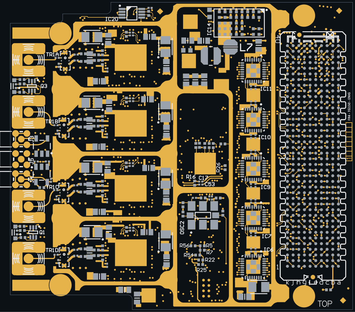
Design review
Probe recorded 20 findings: 1 blocker · 9 major · 10 minor (104 items) on this design. Each is shown here with its reasoning; the full review links every one to the pins, nets and datasheet pages it rests on.
- NetCopperSplitblockerOpen
NetCopperSplit: 5 boards×5
Refuted once, awaiting a second check · Claude walker W1 (Cern session)
At split:GND, split:NetJ1_2, split:NetJ2_2, split:NetJ8_2, split:NetJ9_2
Each finding, with its own headline
split:GNDGND's copper is in 2 pieces: R24.1 is not connected to the rest of the net
GND's copper is in 2 pieces: R24.1 is not connected to the rest of the net. Piece 1: B1.1, B10.1, B11.1, B14.1, B15.1, B16.1, B4.1, B5.1 and 549 more pin(s), on TOP_LAYER, GND_SMAGND_, L3, L5 and BOTTOM_LAYER, 624 drill(s), 5243.59 mm2 of pour, over (0.34, 0.49) to (76.15, 68.83). Piece 2: R24.1, on BOTTOM_LAYER, over (2.98, 34.45) to (5.56, 36.62). The export files every one of these pins under the net, so every connectivity check passes; the copper the fab builds leaves them apart. Usually a pour island that touches only one via of its own net, or a track ending short of its copper: join the piece to the net and export again.
split:NetJ1_2NetJ1_2's copper is in 3 pieces: C55D.1 and 1 other piece(s) are not connected to the rest of the net
NetJ1_2's copper is in 3 pieces: C55D.1 and 1 other piece(s) are not connected to the rest of the net. Piece 1: C54D.2, C9D.2 and R41D.2, on BOTTOM_LAYER, over (0.35, 7.87) to (7.86, 16.03). Piece 2: C55D.1, on TOP_LAYER, GND_SMAGND_, L3, L5 and BOTTOM_LAYER, 2 drill(s), 52.78 mm2 of pour, over (0.34, 7.67) to (12, 15.63). Piece 3: J1.2, on TOP_LAYER, over (0.35, 7.87) to (7.86, 15.38). The export files every one of these pins under the net, so every connectivity check passes; the copper the fab builds leaves them apart. Usually a pour island that touches only one via of its own net, or a track ending short of its copper: join the piece to the net and export again.
split:NetJ2_2NetJ2_2's copper is in 3 pieces: C55C.1 and 1 other piece(s) are not connected to the rest of the net
NetJ2_2's copper is in 3 pieces: C55C.1 and 1 other piece(s) are not connected to the rest of the net. Piece 1: C54C.2, C9C.2 and R41C.2, on BOTTOM_LAYER, over (0.35, 18.93) to (7.86, 27.08). Piece 2: C55C.1, on TOP_LAYER, GND_SMAGND_, L3, L5 and BOTTOM_LAYER, 2 drill(s), 65.85 mm2 of pour, over (0.34, 19.37) to (12, 29.63). Piece 3: J2.2, on TOP_LAYER, over (0.35, 19.58) to (7.86, 27.08). The export files every one of these pins under the net, so every connectivity check passes; the copper the fab builds leaves them apart. Usually a pour island that touches only one via of its own net, or a track ending short of its copper: join the piece to the net and export again.
split:NetJ8_2NetJ8_2's copper is in 3 pieces: C55B.1 and 1 other piece(s) are not connected to the rest of the net
NetJ8_2's copper is in 3 pieces: C55B.1 and 1 other piece(s) are not connected to the rest of the net. Piece 1: C54B.2, C9B.2 and R41B.2, on BOTTOM_LAYER, over (0.35, 40.13) to (7.86, 49.23). Piece 2: C55B.1, on TOP_LAYER, GND_SMAGND_, L3, L5 and BOTTOM_LAYER, 2 drill(s), 70.27 mm2 of pour, over (0.34, 38.14) to (12, 48.28). Piece 3: J8.2, on TOP_LAYER, over (0.35, 40.76) to (7.86, 48.28). The export files every one of these pins under the net, so every connectivity check passes; the copper the fab builds leaves them apart. Usually a pour island that touches only one via of its own net, or a track ending short of its copper: join the piece to the net and export again.
split:NetJ9_2NetJ9_2's copper is in 3 pieces: C55A.1 and 1 other piece(s) are not connected to the rest of the net
NetJ9_2's copper is in 3 pieces: C55A.1 and 1 other piece(s) are not connected to the rest of the net. Piece 1: C54A.2, C9A.2 and R41A.2, on BOTTOM_LAYER, over (0.35, 51.75) to (7.86, 59.98). Piece 2: C55A.1, on TOP_LAYER, GND_SMAGND_, L3, L5 and BOTTOM_LAYER, 2 drill(s), 52.96 mm2 of pour, over (0.34, 52.29) to (12, 59.98). Piece 3: J9.2, on TOP_LAYER, over (0.35, 52.47) to (7.86, 59.98). The export files every one of these pins under the net, so every connectivity check passes; the copper the fab builds leaves them apart. Usually a pour island that touches only one via of its own net, or a track ending short of its copper: join the piece to the net and export again.
IC26 PCA9306: VREF2 tied straight to P3V3CLK (no 200k) and EN pulled to 3.3 V - the datasheet's 'improper set up', which back-feeds VADJ and can overstress the pass FET
The Si571 (OSC2) I2C translator IC26 (PCA9306) has VREF2 tied straight to P3V3CLK with no 200k resistor and EN pulled to 3.3 V through R55. This is the datasheet's "improper set up": whenever VADJ is set more than about 0.6 V below 3.3 V it back-feeds VADJ through the reference FET with nothing to limit the current.
Where it is
Pin As built Datasheet normal set-up Source VREF1 (pin 2) VADJ, the carrier's adjustable 1.2-3.3 V FMC rail VCC1 side netlist VREF2 (pin 7) directly on P3V3CLK (the IC17 LDO output, 51 members), no series resistor shorted to EN and tied to VCC2 through a 200 kOhm resistor, so VREF2 settles at VREF1 + Vth netlist; PCA9306 SCPS113O p.10, 8.1.2 EN (pin 8) R55 10k to P3V3CLK, not shorted to VREF2 shorted to VREF2 netlist; SCPS113O p.10 ``
mermaid flowchart LR A["P3V3CLK<br/>stiff 3.3 V"] -- "no resistor" --> B["IC26 VREF2, pin 7"] C["R55 10k"] --> D["IC26 EN, pin 8<br/>gate at 3.3 V"] B --> E["reference FET"] E -- "unlimited current" --> F["IC26 VREF1, pin 2<br/>VADJ 1.8 or 2.5 V"]``Why it matters
Quantity Value Source Concern arises when VCC2 exceeds VCC1 by Vth, about 0.6 V PCA9306 SCPS113O, p.11 Continuous channel current, absolute maximum 128 mA PCA9306 SCPS113O, p.5 Whenever the carrier sets VADJ more than about 0.6 V below 3.3 V (e.g. VADJ = 2.5 V or 1.8 V, both legal VITA 57.1 settings), the reference FET conducts from P3V3CLK into VADJ with nothing but the FET to limit the current. The datasheet (p.11) says "If VREF2 is tied directly to the VCC2 rail without a resistor, then there is no external resistance ... to limit the current", calls Figure 8-2 "an improper set up", and warns this potentially breaks the pass FET above the 128 mA continuous channel current.
Remedy per datasheet: a series 200k from P3V3CLK to VREF2, with EN tied to VREF2. R55 can remain as the 200k position if resized and VREF2 is moved onto its net.
- PartLifecyclemajorOpen
BAR66 on D1: the distributor catalogue reports "Obsolete" for Infineon Technologies's BAR66
BAR66 on D1: the distributor catalogue reports "Obsolete" for Infineon Technologies's BAR66 — a sourcing/longevity risk to confirm against the MANUFACTURER before acting. That is the maker this board's BOM names (INFINEON). A distributor delisting is not the same claim as the part being unavailable; check the vendor's own lifecycle/product-change notice for the status and any named successor. Re-read the source: GET /api/odb/parts/BAR66/providers (which provider said it, the maker and part number it matched, its own words, and when we asked). No approved alternate is recorded for this position.
At D1
- DecapOrdermajorOpen
DecapOrder: 5 components×5
Checked by the review, stands · Claude walker W3 (Cern session) — Checked: the distances are read from placement as stated. This is a layout-practice heuristic (Probe's starting thresholds); no datasheet on file fixes the order of these values at the 1-5 mm scale, where via and plane-spreading inductance usually dominate. Left for the owner.
At IC11, IC13, IC7, IC8, IC9
Each finding, with its own headline
IC11IC11 supply pins 19, 20 on 'P3V3_BUF': the smallest capacitor C97 sits 2.3 mm away, behind C106 at 0.4 mm
IC11 supply pins 19, 20 on 'P3V3_BUF': the smallest capacitor C97 sits 2.3 mm away, behind C106 at 0.4 mm. IC11.19: the smallest value, C97 (10 nF), is 2.3 mm from the pin and C106 (100 nF) 0.4 mm: the high-frequency part sits behind more inductance than the bulk part, which needs it least. IC11.20: the smallest value, C97 (10 nF), is 1.8 mm from the pin and C106 (100 nF) 0.4 mm: the high-frequency part sits behind more inductance than the bulk part, which needs it least. Swap them, or bring the smallest value to the pin: it serves the fastest current and is the one the loop inductance defeats. Distances are pad centre to pin centre in the board plane. The 5 mm radius, the 10x value step and the 1 mm / 1.5x tie tolerance are Probe's starting values.
IC13IC13 supply pins 19, 20, 21 on 'P3V3_BUF': the smallest capacitor C97 sits 2.5 mm away, behind C105 at 0.4 mm
IC13 supply pins 19, 20, 21 on 'P3V3_BUF': the smallest capacitor C97 sits 2.5 mm away, behind C105 at 0.4 mm. IC13.19: the smallest value, C97 (10 nF), is 2.5 mm from the pin and C105 (100 nF) 0.4 mm: the high-frequency part sits behind more inductance than the bulk part, which needs it least. IC13.20: the smallest value, C97 (10 nF), is 2.0 mm from the pin and C105 (100 nF) 0.4 mm: the high-frequency part sits behind more inductance than the bulk part, which needs it least. IC13.21: the smallest value, C97 (10 nF), is 1.6 mm from the pin and C99 (100 nF) 0.4 mm: the high-frequency part sits behind more inductance than the bulk part, which needs it least. Swap them, or bring the smallest value to the pin: it serves the fastest current and is the one the loop inductance defeats. Distances are pad centre to pin centre in the board plane. The 5 mm radius, the 10x value step and the 1 mm / 1.5x tie tolerance are Probe's starting values.
IC7IC7 supply pins 6, 7 on 'P3V3_BUF': the smallest capacitor C111 sits 1.6 mm away, behind C116 at 0.3 mm
IC7 supply pins 6, 7 on 'P3V3_BUF': the smallest capacitor C111 sits 1.6 mm away, behind C116 at 0.3 mm. IC7.6: the smallest value, C111 (10 nF), is 1.6 mm from the pin and C116 (100 nF) 0.3 mm: the high-frequency part sits behind more inductance than the bulk part, which needs it least. IC7.7: the smallest value, C111 (10 nF), is 2.0 mm from the pin and C116 (100 nF) 0.5 mm: the high-frequency part sits behind more inductance than the bulk part, which needs it least. Swap them, or bring the smallest value to the pin: it serves the fastest current and is the one the loop inductance defeats. Distances are pad centre to pin centre in the board plane. The 5 mm radius, the 10x value step and the 1 mm / 1.5x tie tolerance are Probe's starting values.
IC8IC8 supply pins 19, 20, 21, 22 on 'P3V3_BUF': the smallest capacitor C111 sits 4.7 mm away, behind C94 at 0.4 mm
IC8 supply pins 19, 20, 21, 22 on 'P3V3_BUF': the smallest capacitor C111 sits 4.7 mm away, behind C94 at 0.4 mm. IC8.19: the smallest value, C111 (10 nF), is 4.7 mm from the pin and C94 (100 nF) 0.4 mm: the high-frequency part sits behind more inductance than the bulk part, which needs it least. IC8.20: the smallest value, C111 (10 nF), is 4.6 mm from the pin and C94 (100 nF) 0.4 mm: the high-frequency part sits behind more inductance than the bulk part, which needs it least. IC8.21: the smallest value, C111 (10 nF), is 4.6 mm from the pin and C100 (100 nF) 0.4 mm: the high-frequency part sits behind more inductance than the bulk part, which needs it least. IC8.22: the smallest value, C111 (10 nF), is 4.6 mm from the pin and C100 (100 nF) 0.4 mm: the high-frequency part sits behind more inductance than the bulk part, which needs it least. Swap them, or bring the smallest value to the pin: it serves the fastest current and is the one the loop inductance defeats. Distances are pad centre to pin centre in the board plane. The 5 mm radius, the 10x value step and the 1 mm / 1.5x tie tolerance are Probe's starting values.
IC9IC9 supply pins 6, 7 on 'P3V3_BUF': the smallest capacitor C113 sits 1.6 mm away, behind C78 at 0.4 mm
IC9 supply pins 6, 7 on 'P3V3_BUF': the smallest capacitor C113 sits 1.6 mm away, behind C78 at 0.4 mm. IC9.6: the smallest value, C113 (10 nF), is 1.6 mm from the pin and C78 (100 nF) 0.4 mm: the high-frequency part sits behind more inductance than the bulk part, which needs it least. IC9.7: the smallest value, C113 (10 nF), is 2.0 mm from the pin and C78 (100 nF) 0.8 mm: the high-frequency part sits behind more inductance than the bulk part, which needs it least. Swap them, or bring the smallest value to the pin: it serves the fastest current and is the one the loop inductance defeats. Distances are pad centre to pin centre in the board plane. The 5 mm radius, the 10x value step and the 1 mm / 1.5x tie tolerance are Probe's starting values.
- DiffPairMismatchmajorOpen
DiffPairMismatch: 2 nets×2
Checked by the review, stands · Claude walker (cern session) — LA28 and LA29 are used single-ended, not as differential pairs. LA28_N goes to IC15 (AMC7823) pin 2 and LA28_P is unused (J6.h31 only); LA29_P drives Q1 gate pin 2 and LA29_N is unused (J6.g31 only). The asymmetry is real and deliberate, with no routing consequence. Stands as stated.
At LA28_P, LA29_N
Each finding, with its own headline
LA28_P'LA28_P' / 'LA28_N' (pair inferred from names) is pin-count asymmetric (1 vs 2)
Differential pair 'LA28_P' / 'LA28_N', INFERRED FROM THE NET NAMES (nothing in the design declares it a pair), is pin-count asymmetric (1 vs 2) - one side reaches a pin the other does not, so the two halves cannot be routed as a matched pair. NOTE: this check does not verify WHICH contact either net reaches; a correctly-symmetric pair can still be swapped at a connector.
LA29_N'LA29_N' / 'LA29_P' (pair inferred from names) is pin-count asymmetric (1 vs 2)
Differential pair 'LA29_N' / 'LA29_P', INFERRED FROM THE NET NAMES (nothing in the design declares it a pair), is pin-count asymmetric (1 vs 2) - one side reaches a pin the other does not, so the two halves cannot be routed as a matched pair. NOTE: this check does not verify WHICH contact either net reaches; a correctly-symmetric pair can still be swapped at a connector.
- PartLifecyclemajorOpen
PartLifecycle: 3 part numbers×3
2 Obsolete, 1 Not For New Designs · on 13 placements
At IC10, L7, Q1
Each finding, with its own headline
IC10DS90LV804TSQ on 9 placements (IC10, IC11, IC12, IC13, IC5, IC6, IC7, IC8, …): the distributor catalogue reports "Obsolete" for Texas Instruments's DS90LV804TSQ
DS90LV804TSQ on 9 placements (IC10, IC11, IC12, IC13, IC5, IC6, IC7, IC8, …): the distributor catalogue reports "Obsolete" for Texas Instruments's DS90LV804TSQ — a sourcing/longevity risk to confirm against the MANUFACTURER before acting. That is the maker this board's BOM names (TEXAS INSTRUMENTS). A distributor delisting is not the same claim as the part being unavailable; check the vendor's own lifecycle/product-change notice for the status and any named successor. Re-read the source: GET /api/odb/parts/DS90LV804TSQ/providers (which provider said it, the maker and part number it matched, its own words, and when we asked). THE LAST BUY DATE HAS PASSED (2025-04-10, 584 day(s) ago), so this is a substitution rather than a buy. The distributor reports NONE left. No approved alternate is recorded for this position.
L7ELLVGG2R2N on L7: the distributor catalogue reports "Obsolete" for Panasonic Industry's ELL-VGG2R2N
ELLVGG2R2N on L7: the distributor catalogue reports "Obsolete" for Panasonic Industry's ELL-VGG2R2N — a sourcing/longevity risk to confirm against the MANUFACTURER before acting. That is the maker this board's BOM names (PANASONIC). A distributor delisting is not the same claim as the part being unavailable; check the vendor's own lifecycle/product-change notice for the status and any named successor. Re-read the source: GET /api/odb/parts/ELLVGG2R2N/providers (which provider said it, the maker and part number it matched, its own words, and when we asked). THE LAST BUY DATE HAS PASSED (2019-09-25, 2,608 day(s) ago), so this is a substitution rather than a buy. The distributor reports NONE left. No approved alternate is recorded for this position.
Q1PMGD280UN on 3 placements (Q1, Q2, Q3): the distributor catalogue reports "Not For New Designs" for Nexperia USA Inc.'s PMGD280UN,115
PMGD280UN on 3 placements (Q1, Q2, Q3): the distributor catalogue reports "Not For New Designs" for Nexperia USA Inc.'s PMGD280UN,115 — a sourcing/longevity risk to confirm against the MANUFACTURER before acting. This board's BOM names NXP SEMICONDUCTORS, and that is one line with Nexperia USA Inc.: NXP's Standard Products business became Nexperia on 2017-02-06; NXP still sells its other lines under its own name. A distributor delisting is not the same claim as the part being unavailable; check the vendor's own lifecycle/product-change notice for the status and any named successor. Re-read the source: GET /api/odb/parts/PMGD280UN/providers (which provider said it, the maker and part number it matched, its own words, and when we asked). No approved alternate is recorded for this position.
- ReferencePlaneDiscontinuitymajorOpen
ReferencePlaneDiscontinuity: 10 boards×10
Checked by the review, stands · Claude walker W3 (Cern session) — Checked: the reference break is read from the copper as stated. Whether it matters depends on the signal's edge rate and the receiver's margin, which no datasheet or app note on file fixes for this net; the impedance step and reflection figures are Probe's model, and the thresholds are its starting values. Layout practice, not a datasheet requirement. Left for the owner.
At refchange:GND|P1V8AB, refchange:GND|P1V8AD, refchange:GND|P1V8DA, refchange:GND|P1V8DB, refchange:GND|P1V8DC, refchange:GND|P3V3 and 4 more
Each finding, with its own headline
refchange:GND|P1V8AB8 nets change reference between GND and P1V8AB at 8 vias, none with a reference that continues across (fastest: ADC_BUF_SDI at 100 ps 10-90 %, ASSUMED)
At 8 via(s), on 8 net(s), the signal leaves a layer referenced by one of GND and P1V8AB for a layer referenced by the other, and no plane references both layers. Different nets: no via can carry the return across; only decoupling between the two planes near the via can. The capacitor carrying the return across was measured at each via, at the knee of the crossing net's edge against 50 ohm assumed: 8 with none. 8 of them at an ASSUMED edge (no edge on file for the net): state one (net_timing_state) and it is re-read. One decision covers the pair: whether GND and P1V8AB are decoupled to each other near these vias. A via whose layers have more references than these two is a site of each pair it joins. None is partial: at every one, no reference continues across the via.
- 'CLKDIVRST_P' at (25.72, 45.84), L3 -> BOTTOM_LAYER: GND on GND_SMAGND_, GND on GND to P1V8AB on POWER; pure, no reference continues across; stitching none, 6.5 mm of track past the via on BOTTOM_LAYER: At the 5 GHz knee of a 100 ps edge (1 ns 10-90 %, assumed: no edge is on file for the net) no capacitor carries the return; only the planes do. GND and P1V8AB are not a thin pair (at most 0.2 mm), so their own capacitance does not carry the return. To serve it, change layers across the same plane, or move the signal to a layer referenced to ground. Measured for reference: C3B (100 nF 0201) 2.4 mm away: 1.89 nH in the 1.600 mm cavity + 0.21 nH ESL + 1.76 nH mounting (pad 0.05 nH (vias beside the pads) + 1 via pair(s) at 1.04 mm pitch, 0.20 mm drill, 1.83 mm to the farther plane): 121.4 ohm at the knee, 243 % of 50 ohm (assumed track impedance). None.
- 'ADC_BUF_RESETN' at (23.35, 46.11), L3 -> BOTTOM_LAYER: GND on GND to P1V8AB on POWER; pure, no reference continues across; stitching none, 4.7 mm of track past the via on BOTTOM_LAYER: At the 5 GHz knee of a 100 ps edge (20 ns 10-90 %, assumed: no edge is on file for the net) no capacitor carries the return; only the planes do. GND and P1V8AB are not a thin pair (at most 0.2 mm), so their own capacitance does not carry the return. To serve it, change layers across the same plane, or move the signal to a layer referenced to ground. Measured for reference: C1B (100 nF 0201) 2.6 mm away: 1.20 nH in the 0.990 mm cavity + 0.21 nH ESL + 0.93 nH mounting (pad 0.05 nH (vias beside the pads) + 1 via pair(s) at 0.60 mm pitch, 0.20 mm drill, 1.22 mm to the farther plane): 73.5 ohm at the knee, 147 % of 50 ohm (assumed track impedance). None.
- 'IPTAT3' at (21.07, 47.89), L3 -> BOTTOM_LAYER: GND on GND to P1V8AB on POWER; pure, no reference continues across; stitching none, 4.5 mm of track past the via on BOTTOM_LAYER: At the 5 GHz knee of a 100 ps edge (100 ps 10-90 %, assumed: no edge is on file for the net) no capacitor carries the return; only the planes do. GND and P1V8AB are not a thin pair (at most 0.2 mm), so their own capacitance does not carry the return. To serve it, change layers across the same plane, or move the signal to a layer referenced to ground. Measured for reference: C2B (100 nF 0201) 2.2 mm away: 1.13 nH in the 0.990 mm cavity + 0.21 nH ESL + 1.20 nH mounting (pad 0.05 nH (vias beside the pads) + 1 via pair(s) at 1.05 mm pitch, 0.20 mm drill, 1.22 mm to the farther plane): 79.6 ohm at the knee, 159 % of 50 ohm (assumed track impedance). None.
- 'ADC_BUF_SCLK' at (25.38, 37.7), L3 -> BOTTOM_LAYER: GND on GND_SMAGND_, GND on GND to P1V8AB on POWER; pure, no reference continues across; stitching none, 4.5 mm of track past the via on BOTTOM_LAYER: At the 5 GHz knee of a 100 ps edge (1 ns 10-90 %, assumed: no edge is on file for the net) no capacitor carries the return; only the planes do. GND and P1V8AB are not a thin pair (at most 0.2 mm), so their own capacitance does not carry the return. To serve it, change layers across the same plane, or move the signal to a layer referenced to ground. Measured for reference: C133B (100 nF 0201) 2.1 mm away: 1.80 nH in the 1.600 mm cavity + 0.21 nH ESL + 1.61 nH mounting (pad 0.05 nH (vias beside the pads) + 1 via pair(s) at 0.84 mm pitch, 0.20 mm drill, 1.83 mm to the farther plane): 113.5 ohm at the knee, 227 % of 50 ohm (assumed track impedance). None.
- 'ADC_BUF_SLEEP' at (23.46, 38.29), L3 -> BOTTOM_LAYER: GND on GND to P1V8AB on POWER; pure, no reference continues across; stitching none, 4.2 mm of track past the via on BOTTOM_LAYER: At the 5 GHz knee of a 100 ps edge (100 ps 10-90 %, assumed: no edge is on file for the net) no capacitor carries the return; only the planes do. GND and P1V8AB are not a thin pair (at most 0.2 mm), so their own capacitance does not carry the return. To serve it, change layers across the same plane, or move the signal to a layer referenced to ground. Measured for reference: C24B (100 nF 0201) 2.2 mm away: 1.13 nH in the 0.990 mm cavity + 0.21 nH ESL + 0.97 nH mounting (pad 0.05 nH (vias beside the pads) + 1 via pair(s) at 0.66 mm pitch, 0.20 mm drill, 1.22 mm to the farther plane): 72.6 ohm at the knee, 145 % of 50 ohm (assumed track impedance). None.
- 'ADC_BUF_SDI' at (24.83, 37.7), L3 -> BOTTOM_LAYER: GND on GND_SMAGND_, GND on GND to P1V8AB on POWER; pure, no reference continues across; stitching none, 4.1 mm of track past the via on BOTTOM_LAYER: At the 5 GHz knee of a 100 ps edge (100 ps 10-90 %, assumed: no edge is on file for the net) no capacitor carries the return; only the planes do. GND and P1V8AB are not a thin pair (at most 0.2 mm), so their own capacitance does not carry the return. To serve it, change layers across the same plane, or move the signal to a layer referenced to ground. Measured for reference: C133B (100 nF 0201) 1.9 mm away: 1.74 nH in the 1.600 mm cavity + 0.21 nH ESL + 1.61 nH mounting (pad 0.05 nH (vias beside the pads) + 1 via pair(s) at 0.84 mm pitch, 0.20 mm drill, 1.83 mm to the farther plane): 111.8 ohm at the knee, 224 % of 50 ohm (assumed track impedance). None.
- 'CLKCB_P' at (24.77, 46.26), TOP_LAYER -> BOTTOM_LAYER: GND on GND_SMAGND_ to P1V8AB on POWER; pure, no reference continues across; stitching none, 0.7 mm of track past the via on BOTTOM_LAYER: At the 5 GHz knee of a 100 ps edge (1 ns 10-90 %, assumed: no edge is on file for the net) no capacitor carries the return; only the planes do. GND and P1V8AB are not a thin pair (at most 0.2 mm), so their own capacitance does not carry the return. To serve it, change layers across the same plane, or move the signal to a layer referenced to ground. Measured for reference: C52B (2.2 uF 0603) 2.6 mm away: 1.94 nH in the 1.600 mm cavity + 0.51 nH ESL + 1.20 nH mounting (pad 0.10 nH + no via of the first net within 1 mm of its pad: the study's 0.6 nH per mm of 1.83 mm depth, ASSUMED): 114.7 ohm at the knee, 229 % of 50 ohm (assumed track impedance). None.
- 'CLKCB_N' at (25.33, 46.24), TOP_LAYER -> BOTTOM_LAYER: GND on GND_SMAGND_ to P1V8AB on POWER; pure, no reference continues across; stitching none, 0.7 mm of track past the via on BOTTOM_LAYER: At the 5 GHz knee of a 100 ps edge (1 ns 10-90 %, assumed: no edge is on file for the net) no capacitor carries the return; only the planes do. GND and P1V8AB are not a thin pair (at most 0.2 mm), so their own capacitance does not carry the return. To serve it, change layers across the same plane, or move the signal to a layer referenced to ground. Measured for reference: C3B (100 nF 0201) 1.9 mm away: 1.75 nH in the 1.600 mm cavity + 0.21 nH ESL + 1.76 nH mounting (pad 0.05 nH (vias beside the pads) + 1 via pair(s) at 1.04 mm pitch, 0.20 mm drill, 1.83 mm to the farther plane): 116.8 ohm at the knee, 234 % of 50 ohm (assumed track impedance). None.
Every site is a row of this finding's evidence, keyed by net, layers and position. GET /api/odb/boards/23/reference-planes?group=refchange%3AGND%7CP1V8AB serves each with its own layer_image region; all of them lie in x 19.07..27.72, y 35.7..49.89 mm (board frame, Y up).
The reference on each layer is the first plane the track meets leaving the via, anti-pads and the net's own copper skipped. Whether it matters depends on each signal's edge rate, which nothing on file states for these nets: a slow static line crosses a split harmlessly, a fast edge does not.
refchange:GND|P1V8AD9 nets change reference between GND and P1V8AD at 9 vias, none with a reference that continues across (fastest: ADC_BUF_CSB0 at 100 ps 10-90 %, ASSUMED)
At 9 via(s), on 9 net(s), the signal leaves a layer referenced by one of GND and P1V8AD for a layer referenced by the other, and no plane references both layers. Different nets: no via can carry the return across; only decoupling between the two planes near the via can. The capacitor carrying the return across was measured at each via, at the knee of the crossing net's edge against 50 ohm assumed: 9 with none. 9 of them at an ASSUMED edge (no edge on file for the net): state one (net_timing_state) and it is re-read. One decision covers the pair: whether GND and P1V8AD are decoupled to each other near these vias. A via whose layers have more references than these two is a site of each pair it joins. None is partial: at every one, no reference continues across the via.
- 'CLKDIVRST_P' at (25.74, 16.75), L3 -> BOTTOM_LAYER: GND on GND_SMAGND_, GND on GND to P1V8AD on POWER; pure, no reference continues across; stitching none, 6.5 mm of track past the via on BOTTOM_LAYER: At the 5 GHz knee of a 100 ps edge (1 ns 10-90 %, assumed: no edge is on file for the net) no capacitor carries the return; only the planes do. GND and P1V8AD are not a thin pair (at most 0.2 mm), so their own capacitance does not carry the return. To serve it, change layers across the same plane, or move the signal to a layer referenced to ground. Measured for reference: C3D (100 nF 0201) 2.5 mm away: 1.90 nH in the 1.600 mm cavity + 0.21 nH ESL + 1.79 nH mounting (pad 0.05 nH (vias beside the pads) + 1 via pair(s) at 1.08 mm pitch, 0.20 mm drill, 1.83 mm to the farther plane): 122.5 ohm at the knee, 245 % of 50 ohm (assumed track impedance). None.
- 'IPTAT1' at (21.27, 19.55), L3 -> BOTTOM_LAYER: GND on GND to P1V8AD on POWER; pure, no reference continues across; stitching none, 5.5 mm of track past the via on BOTTOM_LAYER: At the 5 GHz knee of a 100 ps edge (100 ps 10-90 %, assumed: no edge is on file for the net) no capacitor carries the return; only the planes do. GND and P1V8AD are not a thin pair (at most 0.2 mm), so their own capacitance does not carry the return. To serve it, change layers across the same plane, or move the signal to a layer referenced to ground. Measured for reference: C2D (100 nF 0201) 2.1 mm away: 1.10 nH in the 0.990 mm cavity + 0.21 nH ESL + 1.22 nH mounting (pad 0.05 nH (vias beside the pads) + 1 via pair(s) at 1.11 mm pitch, 0.20 mm drill, 1.22 mm to the farther plane): 79.7 ohm at the knee, 159 % of 50 ohm (assumed track impedance). None.
- 'ADC_BUF_RESETN' at (23.38, 17.05), L3 -> BOTTOM_LAYER: GND on GND to P1V8AD on POWER; pure, no reference continues across; stitching none, 4.7 mm of track past the via on BOTTOM_LAYER: At the 5 GHz knee of a 100 ps edge (20 ns 10-90 %, assumed: no edge is on file for the net) no capacitor carries the return; only the planes do. GND and P1V8AD are not a thin pair (at most 0.2 mm), so their own capacitance does not carry the return. To serve it, change layers across the same plane, or move the signal to a layer referenced to ground. Measured for reference: C1D (100 nF 0201) 2.6 mm away: 1.20 nH in the 0.990 mm cavity + 0.21 nH ESL + 0.93 nH mounting (pad 0.05 nH (vias beside the pads) + 1 via pair(s) at 0.60 mm pitch, 0.20 mm drill, 1.22 mm to the farther plane): 73.5 ohm at the knee, 147 % of 50 ohm (assumed track impedance). None.
- 'ADC_BUF_SCLK' at (25.41, 8.64), L3 -> BOTTOM_LAYER: GND on GND_SMAGND_, GND on GND to P1V8AD on POWER; pure, no reference continues across; stitching none, 4.5 mm of track past the via on BOTTOM_LAYER: At the 5 GHz knee of a 100 ps edge (1 ns 10-90 %, assumed: no edge is on file for the net) no capacitor carries the return; only the planes do. GND and P1V8AD are not a thin pair (at most 0.2 mm), so their own capacitance does not carry the return. To serve it, change layers across the same plane, or move the signal to a layer referenced to ground. Measured for reference: C133D (100 nF 0201) 2.2 mm away: 1.82 nH in the 1.600 mm cavity + 0.21 nH ESL + 1.49 nH mounting (pad 0.05 nH (vias beside the pads) + 1 via pair(s) at 0.71 mm pitch, 0.20 mm drill, 1.83 mm to the farther plane): 110.6 ohm at the knee, 221 % of 50 ohm (assumed track impedance). None.
- 'ADC_BUF_SLEEP' at (23.47, 9.1), L3 -> BOTTOM_LAYER: GND on GND to P1V8AD on POWER; pure, no reference continues across; stitching none, 4.2 mm of track past the via on BOTTOM_LAYER: At the 5 GHz knee of a 100 ps edge (100 ps 10-90 %, assumed: no edge is on file for the net) no capacitor carries the return; only the planes do. GND and P1V8AD are not a thin pair (at most 0.2 mm), so their own capacitance does not carry the return. To serve it, change layers across the same plane, or move the signal to a layer referenced to ground. Measured for reference: C24D (100 nF 0201) 2.1 mm away: 1.10 nH in the 0.990 mm cavity + 0.21 nH ESL + 0.97 nH mounting (pad 0.05 nH (vias beside the pads) + 1 via pair(s) at 0.66 mm pitch, 0.20 mm drill, 1.22 mm to the farther plane): 71.8 ohm at the knee, 144 % of 50 ohm (assumed track impedance). None.
- 'ADC_BUF_SDI' at (24.85, 8.64), L3 -> BOTTOM_LAYER: GND on GND_SMAGND_, GND on GND to P1V8AD on POWER; pure, no reference continues across; stitching none, 4.1 mm of track past the via on BOTTOM_LAYER: At the 5 GHz knee of a 100 ps edge (100 ps 10-90 %, assumed: no edge is on file for the net) no capacitor carries the return; only the planes do. GND and P1V8AD are not a thin pair (at most 0.2 mm), so their own capacitance does not carry the return. To serve it, change layers across the same plane, or move the signal to a layer referenced to ground. Measured for reference: C133D (100 nF 0201) 2.0 mm away: 1.76 nH in the 1.600 mm cavity + 0.21 nH ESL + 1.49 nH mounting (pad 0.05 nH (vias beside the pads) + 1 via pair(s) at 0.71 mm pitch, 0.20 mm drill, 1.83 mm to the farther plane): 108.7 ohm at the knee, 217 % of 50 ohm (assumed track impedance). None.
- 'ADC_BUF_CSB0' at (26.04, 9.27), L3 -> BOTTOM_LAYER: GND on GND_SMAGND_, GND on GND to P1V8AD on POWER; pure, no reference continues across; stitching none, 3.0 mm of track past the via on BOTTOM_LAYER: At the 5 GHz knee of a 100 ps edge (100 ps 10-90 %, assumed: no edge is on file for the net) no capacitor carries the return; only the planes do. GND and P1V8AD are not a thin pair (at most 0.2 mm), so their own capacitance does not carry the return. To serve it, change layers across the same plane, or move the signal to a layer referenced to ground. None.
- 'CLKCD_P' at (24.8, 17.2), TOP_LAYER -> BOTTOM_LAYER: GND on GND_SMAGND_ to P1V8AD on POWER; pure, no reference continues across; stitching none, 0.7 mm of track past the via on BOTTOM_LAYER: At the 5 GHz knee of a 100 ps edge (1 ns 10-90 %, assumed: no edge is on file for the net) no capacitor carries the return; only the planes do. GND and P1V8AD are not a thin pair (at most 0.2 mm), so their own capacitance does not carry the return. To serve it, change layers across the same plane, or move the signal to a layer referenced to ground. Measured for reference: C4D (100 nF 0201) 2.0 mm away: 1.75 nH in the 1.600 mm cavity + 0.21 nH ESL + 1.75 nH mounting (pad 0.05 nH (vias beside the pads) + 1 via pair(s) at 1.02 mm pitch, 0.20 mm drill, 1.83 mm to the farther plane): 116.7 ohm at the knee, 233 % of 50 ohm (assumed track impedance). None.
- 'CLKCD_N' at (25.36, 17.17), TOP_LAYER -> BOTTOM_LAYER: GND on GND_SMAGND_ to P1V8AD on POWER; pure, no reference continues across; stitching none, 0.7 mm of track past the via on BOTTOM_LAYER: At the 5 GHz knee of a 100 ps edge (1 ns 10-90 %, assumed: no edge is on file for the net) no capacitor carries the return; only the planes do. GND and P1V8AD are not a thin pair (at most 0.2 mm), so their own capacitance does not carry the return. To serve it, change layers across the same plane, or move the signal to a layer referenced to ground. Measured for reference: C3D (100 nF 0201) 1.9 mm away: 1.75 nH in the 1.600 mm cavity + 0.21 nH ESL + 1.79 nH mounting (pad 0.05 nH (vias beside the pads) + 1 via pair(s) at 1.08 mm pitch, 0.20 mm drill, 1.83 mm to the farther plane): 117.8 ohm at the knee, 236 % of 50 ohm (assumed track impedance). None.
Every site is a row of this finding's evidence, keyed by net, layers and position. GET /api/odb/boards/23/reference-planes?group=refchange%3AGND%7CP1V8AD serves each with its own layer_image region; all of them lie in x 19.27..28.04, y 6.64..21.55 mm (board frame, Y up).
The reference on each layer is the first plane the track meets leaving the via, anti-pads and the net's own copper skipped. Whether it matters depends on each signal's edge rate, which nothing on file states for these nets: a slow static line crosses a split harmlessly, a fast edge does not.
refchange:GND|P1V8DA13 nets change reference between GND and P1V8DA at 13 vias, none with a reference that continues across (fastest: ADC_BUF_SDO at 100 ps 10-90 %, ASSUMED)
At 13 via(s), on 13 net(s), the signal leaves a layer referenced by one of GND and P1V8DA for a layer referenced by the other, and no plane references both layers. Different nets: no via can carry the return across; only decoupling between the two planes near the via can. The capacitor carrying the return across was measured at each via, at the knee of the crossing net's edge against 50 ohm assumed: 13 with none. 13 of them at an ASSUMED edge (no edge on file for the net): state one (net_timing_state) and it is re-read. One decision covers the pair: whether GND and P1V8DA are decoupled to each other near these vias. A via whose layers have more references than these two is a site of each pair it joins. None is partial: at every one, no reference continues across the via.
- 'ADC_BUF_SDO' at (26.77, 52.92), L3 -> BOTTOM_LAYER: GND on GND_SMAGND_, GND on GND to P1V8DA on POWER; pure, no reference continues across; stitching none, 6.7 mm of track past the via on BOTTOM_LAYER: At the 5 GHz knee of a 100 ps edge (100 ps 10-90 %, assumed: no edge is on file for the net) no capacitor carries the return; only the planes do. GND and P1V8DA are not a thin pair (at most 0.2 mm), so their own capacitance does not carry the return. To serve it, change layers across the same plane, or move the signal to a layer referenced to ground. Measured for reference: C11A (100 nF 0201) 2.7 mm away: 1.96 nH in the 1.600 mm cavity + 0.21 nH ESL + 1.54 nH mounting (pad 0.05 nH (vias beside the pads) + 1 via pair(s) at 0.76 mm pitch, 0.20 mm drill, 1.83 mm to the farther plane): 116.5 ohm at the knee, 233 % of 50 ohm (assumed track impedance). None.
- 'ADC_DATA3.D2_P' at (29.26, 52.44), L3 -> BOTTOM_LAYER: GND on GND_SMAGND_, GND on GND to P1V8DA on POWER; pure, no reference continues across; stitching none, 1.9 mm of track past the via on BOTTOM_LAYER: At the 5 GHz knee of a 100 ps edge (100 ps 10-90 %, assumed: no edge is on file for the net) no capacitor carries the return; only the planes do. GND and P1V8DA are not a thin pair (at most 0.2 mm), so their own capacitance does not carry the return. To serve it, change layers across the same plane, or move the signal to a layer referenced to ground. Measured for reference: C11A (100 nF 0201) 1.7 mm away: 1.65 nH in the 1.600 mm cavity + 0.21 nH ESL + 1.54 nH mounting (pad 0.05 nH (vias beside the pads) + 1 via pair(s) at 0.76 mm pitch, 0.20 mm drill, 1.83 mm to the farther plane): 106.7 ohm at the knee, 213 % of 50 ohm (assumed track impedance). None.
- 'ADC_DATA3.D2_N' at (29.89, 52.44), L3 -> BOTTOM_LAYER: GND on GND_SMAGND_, GND on GND to P1V8DA on POWER; pure, no reference continues across; stitching none, 1.9 mm of track past the via on BOTTOM_LAYER: At the 5 GHz knee of a 100 ps edge (100 ps 10-90 %, assumed: no edge is on file for the net) no capacitor carries the return; only the planes do. GND and P1V8DA are not a thin pair (at most 0.2 mm), so their own capacitance does not carry the return. To serve it, change layers across the same plane, or move the signal to a layer referenced to ground. Measured for reference: C11A (100 nF 0201) 2.0 mm away: 1.77 nH in the 1.600 mm cavity + 0.21 nH ESL + 1.54 nH mounting (pad 0.05 nH (vias beside the pads) + 1 via pair(s) at 0.76 mm pitch, 0.20 mm drill, 1.83 mm to the farther plane): 110.4 ohm at the knee, 221 % of 50 ohm (assumed track impedance). None.
- 'ADC_DATA3.CLKOUT_P' at (31.75, 55.41), L3 -> BOTTOM_LAYER: GND on GND_SMAGND_, GND on GND to P1V8DA on POWER; pure, no reference continues across; stitching none, 1.5 mm of track past the via on BOTTOM_LAYER: At the 5 GHz knee of a 100 ps edge (1 ns 10-90 %, assumed: no edge is on file for the net) no capacitor carries the return; only the planes do. GND and P1V8DA are not a thin pair (at most 0.2 mm), so their own capacitance does not carry the return. To serve it, change layers across the same plane, or move the signal to a layer referenced to ground. None.
- 'ADC_DATA3.CLKOUT_N' at (31.75, 56.03), L3 -> BOTTOM_LAYER: GND on GND_SMAGND_, GND on GND to P1V8DA on POWER; pure, no reference continues across; stitching none, 1.5 mm of track past the via on BOTTOM_LAYER: At the 5 GHz knee of a 100 ps edge (1 ns 10-90 %, assumed: no edge is on file for the net) no capacitor carries the return; only the planes do. GND and P1V8DA are not a thin pair (at most 0.2 mm), so their own capacitance does not carry the return. To serve it, change layers across the same plane, or move the signal to a layer referenced to ground. None.
- 'ADC_DATA3.D8_P' at (31.75, 57.41), L3 -> BOTTOM_LAYER: GND on GND_SMAGND_, GND on GND to P1V8DA on POWER; pure, no reference continues across; stitching none, 0.8 mm of track past the via on BOTTOM_LAYER: At the 5 GHz knee of a 100 ps edge (100 ps 10-90 %, assumed: no edge is on file for the net) no capacitor carries the return; only the planes do. GND and P1V8DA are not a thin pair (at most 0.2 mm), so their own capacitance does not carry the return. To serve it, change layers across the same plane, or move the signal to a layer referenced to ground. None.
- 'ADC_DATA3.D8_N' at (31.75, 58.03), L3 -> BOTTOM_LAYER: GND on GND_SMAGND_, GND on GND to P1V8DA on POWER; pure, no reference continues across; stitching none, 0.8 mm of track past the via on BOTTOM_LAYER: At the 5 GHz knee of a 100 ps edge (100 ps 10-90 %, assumed: no edge is on file for the net) no capacitor carries the return; only the planes do. GND and P1V8DA are not a thin pair (at most 0.2 mm), so their own capacitance does not carry the return. To serve it, change layers across the same plane, or move the signal to a layer referenced to ground. None.
- 'ADC_DATA3.D10_P' at (33.29, 59.41), L3 -> BOTTOM_LAYER: GND on GND_SMAGND_, GND on GND to P1V8DA on POWER; pure, no reference continues across; stitching none, 0.8 mm of track past the via on BOTTOM_LAYER: At the 5 GHz knee of a 100 ps edge (100 ps 10-90 %, assumed: no edge is on file for the net) no capacitor carries the return; only the planes do. GND and P1V8DA are not a thin pair (at most 0.2 mm), so their own capacitance does not carry the return. To serve it, change layers across the same plane, or move the signal to a layer referenced to ground. Measured for reference: C60A (47 uF 1206) 1.5 mm away: 1.59 nH in the 1.600 mm cavity + 0.80 nH ESL + 1.30 nH mounting (pad 0.20 nH + no via of the first net within 1 mm of its pad: the study's 0.6 nH per mm of 1.83 mm depth, ASSUMED): 115.8 ohm at the knee, 232 % of 50 ohm (assumed track impedance). None.
- 'ADC_DATA3.D10_N' at (33.29, 60.03), L3 -> BOTTOM_LAYER: GND on GND_SMAGND_, GND on GND to P1V8DA on POWER; pure, no reference continues across; stitching none, 0.8 mm of track past the via on BOTTOM_LAYER: At the 5 GHz knee of a 100 ps edge (100 ps 10-90 %, assumed: no edge is on file for the net) no capacitor carries the return; only the planes do. GND and P1V8DA are not a thin pair (at most 0.2 mm), so their own capacitance does not carry the return. To serve it, change layers across the same plane, or move the signal to a layer referenced to ground. Measured for reference: C134A (2.2 uF 0603) 2.5 mm away: 1.90 nH in the 1.600 mm cavity + 0.51 nH ESL + 1.20 nH mounting (pad 0.10 nH + no via of the first net within 1 mm of its pad: the study's 0.6 nH per mm of 1.83 mm depth, ASSUMED): 113.2 ohm at the knee, 226 % of 50 ohm (assumed track impedance). None.
- 'ADC_DATA3.D14_P' at (29.4, 62.42), L3 -> BOTTOM_LAYER: GND on GND_SMAGND_, GND on GND to P1V8DA on POWER; pure, no reference continues across; stitching none, 0.8 mm of track past the via on BOTTOM_LAYER: At the 5 GHz knee of a 100 ps edge (100 ps 10-90 %, assumed: no edge is on file for the net) no capacitor carries the return; only the planes do. GND and P1V8DA are not a thin pair (at most 0.2 mm), so their own capacitance does not carry the return. To serve it, change layers across the same plane, or move the signal to a layer referenced to ground. Measured for reference: C10A (100 nF 0201) 1.0 mm away: 1.31 nH in the 1.600 mm cavity + 0.21 nH ESL + 1.71 nH mounting (pad 0.05 nH (vias beside the pads) + 1 via pair(s) at 0.96 mm pitch, 0.20 mm drill, 1.83 mm to the farther plane): 101.5 ohm at the knee, 203 % of 50 ohm (assumed track impedance). None.
- 'ADC_DATA3.D14_N' at (28.77, 62.42), L3 -> BOTTOM_LAYER: GND on GND_SMAGND_, GND on GND to P1V8DA on POWER; pure, no reference continues across; stitching none, 0.8 mm of track past the via on BOTTOM_LAYER: At the 5 GHz knee of a 100 ps edge (100 ps 10-90 %, assumed: no edge is on file for the net) no capacitor carries the return; only the planes do. GND and P1V8DA are not a thin pair (at most 0.2 mm), so their own capacitance does not carry the return. To serve it, change layers across the same plane, or move the signal to a layer referenced to ground. Measured for reference: C12A (100 nF 0201) 1.6 mm away: 1.60 nH in the 1.600 mm cavity + 0.21 nH ESL + 1.54 nH mounting (pad 0.05 nH (vias beside the pads) + 1 via pair(s) at 0.76 mm pitch, 0.20 mm drill, 1.83 mm to the farther plane): 105.2 ohm at the knee, 210 % of 50 ohm (assumed track impedance). None.
- 'ADC_DATA3.D0_P' at (27.25, 52.47), L3 -> BOTTOM_LAYER: GND on GND_SMAGND_, GND on GND to P1V8DA on POWER; pure, no reference continues across; stitching none, 0.7 mm of track past the via on BOTTOM_LAYER: At the 5 GHz knee of a 100 ps edge (100 ps 10-90 %, assumed: no edge is on file for the net) no capacitor carries the return; only the planes do. GND and P1V8DA are not a thin pair (at most 0.2 mm), so their own capacitance does not carry the return. To serve it, change layers across the same plane, or move the signal to a layer referenced to ground. Measured for reference: C11A (100 nF 0201) 2.1 mm away: 1.78 nH in the 1.600 mm cavity + 0.21 nH ESL + 1.54 nH mounting (pad 0.05 nH (vias beside the pads) + 1 via pair(s) at 0.76 mm pitch, 0.20 mm drill, 1.83 mm to the farther plane): 110.9 ohm at the knee, 222 % of 50 ohm (assumed track impedance). None.
- and 1 more
Every site is a row of this finding's evidence, keyed by net, layers and position. GET /api/odb/boards/23/reference-planes?group=refchange%3AGND%7CP1V8DA serves each with its own layer_image region; all of them lie in x 24.77..35.29, y 50.44..64.42 mm (board frame, Y up).
The reference on each layer is the first plane the track meets leaving the via, anti-pads and the net's own copper skipped. Whether it matters depends on each signal's edge rate, which nothing on file states for these nets: a slow static line crosses a split harmlessly, a fast edge does not.
refchange:GND|P1V8DB13 nets change reference between GND and P1V8DB at 13 vias, none with a reference that continues across (fastest: ADC_BUF_SDO at 100 ps 10-90 %, ASSUMED)
At 13 via(s), on 13 net(s), the signal leaves a layer referenced by one of GND and P1V8DB for a layer referenced by the other, and no plane references both layers. Different nets: no via can carry the return across; only decoupling between the two planes near the via can. The capacitor carrying the return across was measured at each via, at the knee of the crossing net's edge against 50 ohm assumed: 13 with none. 13 of them at an ASSUMED edge (no edge on file for the net): state one (net_timing_state) and it is re-read. One decision covers the pair: whether GND and P1V8DB are decoupled to each other near these vias. A via whose layers have more references than these two is a site of each pair it joins. None is partial: at every one, no reference continues across the via.
- 'ADC_BUF_SDO' at (26.78, 38.16), L3 -> BOTTOM_LAYER: GND on GND to P1V8DB on POWER; pure, no reference continues across; stitching none, 6.7 mm of track past the via on BOTTOM_LAYER: At the 5 GHz knee of a 100 ps edge (100 ps 10-90 %, assumed: no edge is on file for the net) no capacitor carries the return; only the planes do. GND and P1V8DB are not a thin pair (at most 0.2 mm), so their own capacitance does not carry the return. To serve it, change layers across the same plane, or move the signal to a layer referenced to ground. Measured for reference: C11B (100 nF 0201) 2.7 mm away: 1.21 nH in the 0.990 mm cavity + 0.21 nH ESL + 1.41 nH mounting (pad 0.05 nH (vias beside the pads) + 1 via pair(s) at 1.62 mm pitch, 0.20 mm drill, 1.22 mm to the farther plane): 89.0 ohm at the knee, 178 % of 50 ohm (assumed track impedance). None.
- 'ADC_DATA2.D4_P' at (31.09, 37.77), L3 -> BOTTOM_LAYER: GND on GND_SMAGND_, GND on GND to P1V8DB on POWER; pure, no reference continues across; stitching none, 2.0 mm of track past the via on BOTTOM_LAYER: At the 5 GHz knee of a 100 ps edge (100 ps 10-90 %, assumed: no edge is on file for the net) no capacitor carries the return; only the planes do. GND and P1V8DB are not a thin pair (at most 0.2 mm), so their own capacitance does not carry the return. To serve it, change layers across the same plane, or move the signal to a layer referenced to ground. None.
- 'ADC_DATA2.CLKOUT_P' at (31.76, 40.65), L3 -> BOTTOM_LAYER: GND on GND_SMAGND_, GND on GND to P1V8DB on POWER; pure, no reference continues across; stitching none, 1.8 mm of track past the via on BOTTOM_LAYER: At the 5 GHz knee of a 100 ps edge (1 ns 10-90 %, assumed: no edge is on file for the net) no capacitor carries the return; only the planes do. GND and P1V8DB are not a thin pair (at most 0.2 mm), so their own capacitance does not carry the return. To serve it, change layers across the same plane, or move the signal to a layer referenced to ground. None.
- 'ADC_DATA2.CLKOUT_N' at (31.76, 41.28), L3 -> BOTTOM_LAYER: GND on GND_SMAGND_, GND on GND to P1V8DB on POWER; pure, no reference continues across; stitching none, 1.8 mm of track past the via on BOTTOM_LAYER: At the 5 GHz knee of a 100 ps edge (1 ns 10-90 %, assumed: no edge is on file for the net) no capacitor carries the return; only the planes do. GND and P1V8DB are not a thin pair (at most 0.2 mm), so their own capacitance does not carry the return. To serve it, change layers across the same plane, or move the signal to a layer referenced to ground. None.
- 'ADC_DATA2.D8_P' at (31.76, 42.65), L3 -> BOTTOM_LAYER: GND on GND_SMAGND_, GND on GND to P1V8DB on POWER; pure, no reference continues across; stitching none, 1.5 mm of track past the via on BOTTOM_LAYER: At the 5 GHz knee of a 100 ps edge (100 ps 10-90 %, assumed: no edge is on file for the net) no capacitor carries the return; only the planes do. GND and P1V8DB are not a thin pair (at most 0.2 mm), so their own capacitance does not carry the return. To serve it, change layers across the same plane, or move the signal to a layer referenced to ground. None.
- 'ADC_DATA2.D8_N' at (31.76, 43.28), L3 -> BOTTOM_LAYER: GND on GND_SMAGND_, GND on GND to P1V8DB on POWER; pure, no reference continues across; stitching none, 1.5 mm of track past the via on BOTTOM_LAYER: At the 5 GHz knee of a 100 ps edge (100 ps 10-90 %, assumed: no edge is on file for the net) no capacitor carries the return; only the planes do. GND and P1V8DB are not a thin pair (at most 0.2 mm), so their own capacitance does not carry the return. To serve it, change layers across the same plane, or move the signal to a layer referenced to ground. None.
- 'ADC_DATA2.D14_P' at (29.37, 46.07), L3 -> BOTTOM_LAYER: GND on GND_SMAGND_, GND on GND to P1V8DB on POWER; pure, no reference continues across; stitching none, 0.9 mm of track past the via on BOTTOM_LAYER: At the 5 GHz knee of a 100 ps edge (100 ps 10-90 %, assumed: no edge is on file for the net) no capacitor carries the return; only the planes do. GND and P1V8DB are not a thin pair (at most 0.2 mm), so their own capacitance does not carry the return. To serve it, change layers across the same plane, or move the signal to a layer referenced to ground. Measured for reference: C134B (2.2 uF 0603) 1.9 mm away: 1.74 nH in the 1.600 mm cavity + 0.51 nH ESL + 1.20 nH mounting (pad 0.10 nH + no via of the first net within 1 mm of its pad: the study's 0.6 nH per mm of 1.83 mm depth, ASSUMED): 108.2 ohm at the knee, 216 % of 50 ohm (assumed track impedance). None.
- 'ADC_DATA2.D10_P' at (33.31, 44.65), L3 -> BOTTOM_LAYER: GND on GND_SMAGND_, GND on GND to P1V8DB on POWER; pure, no reference continues across; stitching none, 0.8 mm of track past the via on BOTTOM_LAYER: At the 5 GHz knee of a 100 ps edge (100 ps 10-90 %, assumed: no edge is on file for the net) no capacitor carries the return; only the planes do. GND and P1V8DB are not a thin pair (at most 0.2 mm), so their own capacitance does not carry the return. To serve it, change layers across the same plane, or move the signal to a layer referenced to ground. Measured for reference: C60B (47 uF 1206) 1.5 mm away: 1.58 nH in the 1.600 mm cavity + 0.80 nH ESL + 1.30 nH mounting (pad 0.20 nH + no via of the first net within 1 mm of its pad: the study's 0.6 nH per mm of 1.83 mm depth, ASSUMED): 115.5 ohm at the knee, 231 % of 50 ohm (assumed track impedance). None.
- 'ADC_DATA2.D10_N' at (33.31, 45.28), L3 -> BOTTOM_LAYER: GND on GND_SMAGND_, GND on GND to P1V8DB on POWER; pure, no reference continues across; stitching none, 0.8 mm of track past the via on BOTTOM_LAYER: At the 5 GHz knee of a 100 ps edge (100 ps 10-90 %, assumed: no edge is on file for the net) no capacitor carries the return; only the planes do. GND and P1V8DB are not a thin pair (at most 0.2 mm), so their own capacitance does not carry the return. To serve it, change layers across the same plane, or move the signal to a layer referenced to ground. Measured for reference: C60B (47 uF 1206) 1.6 mm away: 1.64 nH in the 1.600 mm cavity + 0.80 nH ESL + 1.30 nH mounting (pad 0.20 nH + no via of the first net within 1 mm of its pad: the study's 0.6 nH per mm of 1.83 mm depth, ASSUMED): 117.5 ohm at the knee, 235 % of 50 ohm (assumed track impedance). None.
- 'ADC_DATA2.D2_P' at (29.25, 37.71), L3 -> BOTTOM_LAYER: GND on GND_SMAGND_, GND on GND to P1V8DB on POWER; pure, no reference continues across; stitching none, 0.7 mm of track past the via on BOTTOM_LAYER: At the 5 GHz knee of a 100 ps edge (100 ps 10-90 %, assumed: no edge is on file for the net) no capacitor carries the return; only the planes do. GND and P1V8DB are not a thin pair (at most 0.2 mm), so their own capacitance does not carry the return. To serve it, change layers across the same plane, or move the signal to a layer referenced to ground. Measured for reference: C11B (100 nF 0201) 1.7 mm away: 1.65 nH in the 1.600 mm cavity + 0.21 nH ESL + 2.09 nH mounting (pad 0.05 nH (vias beside the pads) + 1 via pair(s) at 1.62 mm pitch, 0.20 mm drill, 1.83 mm to the farther plane): 124.2 ohm at the knee, 248 % of 50 ohm (assumed track impedance). None.
- 'ADC_DATA2.D2_N' at (29.88, 37.71), L3 -> BOTTOM_LAYER: GND on GND_SMAGND_, GND on GND to P1V8DB on POWER; pure, no reference continues across; stitching none, 0.7 mm of track past the via on BOTTOM_LAYER: At the 5 GHz knee of a 100 ps edge (100 ps 10-90 %, assumed: no edge is on file for the net) no capacitor carries the return; only the planes do. GND and P1V8DB are not a thin pair (at most 0.2 mm), so their own capacitance does not carry the return. To serve it, change layers across the same plane, or move the signal to a layer referenced to ground. Measured for reference: C11B (100 nF 0201) 2.0 mm away: 1.77 nH in the 1.600 mm cavity + 0.21 nH ESL + 2.09 nH mounting (pad 0.05 nH (vias beside the pads) + 1 via pair(s) at 1.62 mm pitch, 0.20 mm drill, 1.83 mm to the farther plane): 127.7 ohm at the knee, 255 % of 50 ohm (assumed track impedance). None.
- 'ADC_DATA2.D0_P' at (27.32, 37.68), L3 -> BOTTOM_LAYER: GND on GND_SMAGND_, GND on GND to P1V8DB on POWER; pure, no reference continues across; stitching none, 0.7 mm of track past the via on BOTTOM_LAYER: At the 5 GHz knee of a 100 ps edge (100 ps 10-90 %, assumed: no edge is on file for the net) no capacitor carries the return; only the planes do. GND and P1V8DB are not a thin pair (at most 0.2 mm), so their own capacitance does not carry the return. To serve it, change layers across the same plane, or move the signal to a layer referenced to ground. Measured for reference: C11B (100 nF 0201) 2.0 mm away: 1.76 nH in the 1.600 mm cavity + 0.21 nH ESL + 2.09 nH mounting (pad 0.05 nH (vias beside the pads) + 1 via pair(s) at 1.62 mm pitch, 0.20 mm drill, 1.83 mm to the farther plane): 127.7 ohm at the knee, 255 % of 50 ohm (assumed track impedance). None.
- and 1 more
Every site is a row of this finding's evidence, keyed by net, layers and position. GET /api/odb/boards/23/reference-planes?group=refchange%3AGND%7CP1V8DB serves each with its own layer_image region; all of them lie in x 24.78..35.31, y 35.68..48.07 mm (board frame, Y up).
The reference on each layer is the first plane the track meets leaving the via, anti-pads and the net's own copper skipped. Whether it matters depends on each signal's edge rate, which nothing on file states for these nets: a slow static line crosses a split harmlessly, a fast edge does not.
refchange:GND|P1V8DC14 nets change reference between GND and P1V8DC at 14 vias, none with a reference that continues across (fastest: ADC_BUF_SDO at 100 ps 10-90 %, ASSUMED)
At 14 via(s), on 14 net(s), the signal leaves a layer referenced by one of GND and P1V8DC for a layer referenced by the other, and no plane references both layers. Different nets: no via can carry the return across; only decoupling between the two planes near the via can. The capacitor carrying the return across was measured at each via, at the knee of the crossing net's edge against 50 ohm assumed: 14 with none. 14 of them at an ASSUMED edge (no edge on file for the net): state one (net_timing_state) and it is re-read. One decision covers the pair: whether GND and P1V8DC are decoupled to each other near these vias. A via whose layers have more references than these two is a site of each pair it joins. None is partial: at every one, no reference continues across the via.
- 'ADC_BUF_SDO' at (26.74, 23.6), L3 -> BOTTOM_LAYER: GND on GND to P1V8DC on POWER; pure, no reference continues across; stitching none, 6.7 mm of track past the via on BOTTOM_LAYER: At the 5 GHz knee of a 100 ps edge (100 ps 10-90 %, assumed: no edge is on file for the net) no capacitor carries the return; only the planes do. GND and P1V8DC are not a thin pair (at most 0.2 mm), so their own capacitance does not carry the return. To serve it, change layers across the same plane, or move the signal to a layer referenced to ground. Measured for reference: C11C (100 nF 0201) 2.7 mm away: 1.21 nH in the 0.990 mm cavity + 0.21 nH ESL + 1.33 nH mounting (pad 0.05 nH (vias beside the pads) + 1 via pair(s) at 1.39 mm pitch, 0.20 mm drill, 1.22 mm to the farther plane): 86.6 ohm at the knee, 173 % of 50 ohm (assumed track impedance). None.
- 'ADC_DATA1.D10_P' at (33.27, 30.09), L3 -> BOTTOM_LAYER: GND on GND_SMAGND_, GND on GND to P1V8DC on POWER; pure, no reference continues across; stitching none, 2.0 mm of track past the via on BOTTOM_LAYER: At the 5 GHz knee of a 100 ps edge (100 ps 10-90 %, assumed: no edge is on file for the net) no capacitor carries the return; only the planes do. GND and P1V8DC are not a thin pair (at most 0.2 mm), so their own capacitance does not carry the return. To serve it, change layers across the same plane, or move the signal to a layer referenced to ground. Measured for reference: C60C (47 uF 1206) 1.6 mm away: 1.63 nH in the 1.600 mm cavity + 0.80 nH ESL + 1.30 nH mounting (pad 0.20 nH + no via of the first net within 1 mm of its pad: the study's 0.6 nH per mm of 1.83 mm depth, ASSUMED): 117.1 ohm at the knee, 234 % of 50 ohm (assumed track impedance). None.
- 'ADC_DATA1.D8_P' at (31.72, 28.09), L3 -> BOTTOM_LAYER: GND on GND_SMAGND_, GND on GND to P1V8DC on POWER; pure, no reference continues across; stitching none, 1.9 mm of track past the via on BOTTOM_LAYER: At the 5 GHz knee of a 100 ps edge (100 ps 10-90 %, assumed: no edge is on file for the net) no capacitor carries the return; only the planes do. GND and P1V8DC are not a thin pair (at most 0.2 mm), so their own capacitance does not carry the return. To serve it, change layers across the same plane, or move the signal to a layer referenced to ground. None.
- 'ADC_DATA1.D8_N' at (31.72, 28.71), L3 -> BOTTOM_LAYER: GND on GND_SMAGND_, GND on GND to P1V8DC on POWER; pure, no reference continues across; stitching none, 1.9 mm of track past the via on BOTTOM_LAYER: At the 5 GHz knee of a 100 ps edge (100 ps 10-90 %, assumed: no edge is on file for the net) no capacitor carries the return; only the planes do. GND and P1V8DC are not a thin pair (at most 0.2 mm), so their own capacitance does not carry the return. To serve it, change layers across the same plane, or move the signal to a layer referenced to ground. None.
- 'ADC_DATA1.CLKOUT_P' at (31.72, 26.09), L3 -> BOTTOM_LAYER: GND on GND_SMAGND_, GND on GND to P1V8DC on POWER; pure, no reference continues across; stitching none, 1.6 mm of track past the via on BOTTOM_LAYER: At the 5 GHz knee of a 100 ps edge (1 ns 10-90 %, assumed: no edge is on file for the net) no capacitor carries the return; only the planes do. GND and P1V8DC are not a thin pair (at most 0.2 mm), so their own capacitance does not carry the return. To serve it, change layers across the same plane, or move the signal to a layer referenced to ground. None.
- 'ADC_DATA1.CLKOUT_N' at (31.72, 26.71), L3 -> BOTTOM_LAYER: GND on GND_SMAGND_, GND on GND to P1V8DC on POWER; pure, no reference continues across; stitching none, 1.6 mm of track past the via on BOTTOM_LAYER: At the 5 GHz knee of a 100 ps edge (1 ns 10-90 %, assumed: no edge is on file for the net) no capacitor carries the return; only the planes do. GND and P1V8DC are not a thin pair (at most 0.2 mm), so their own capacitance does not carry the return. To serve it, change layers across the same plane, or move the signal to a layer referenced to ground. None.
- 'ADC_DATA1.D10_N' at (33.28, 30.74), L3 -> BOTTOM_LAYER: GND on GND_SMAGND_, GND on GND to P1V8DC on POWER; pure, no reference continues across; stitching none, 1.5 mm of track past the via on BOTTOM_LAYER: At the 5 GHz knee of a 100 ps edge (100 ps 10-90 %, assumed: no edge is on file for the net) no capacitor carries the return; only the planes do. GND and P1V8DC are not a thin pair (at most 0.2 mm), so their own capacitance does not carry the return. To serve it, change layers across the same plane, or move the signal to a layer referenced to ground. Measured for reference: C134C (2.2 uF 0603) 2.5 mm away: 1.92 nH in the 1.600 mm cavity + 0.51 nH ESL + 1.20 nH mounting (pad 0.10 nH + no via of the first net within 1 mm of its pad: the study's 0.6 nH per mm of 1.83 mm depth, ASSUMED): 113.9 ohm at the knee, 228 % of 50 ohm (assumed track impedance). None.
- 'ADC_DATA1.D4_P' at (31.06, 23.26), L3 -> BOTTOM_LAYER: GND on GND_SMAGND_, GND on GND to P1V8DC on POWER; pure, no reference continues across; stitching none, 0.9 mm of track past the via on BOTTOM_LAYER: At the 5 GHz knee of a 100 ps edge (100 ps 10-90 %, assumed: no edge is on file for the net) no capacitor carries the return; only the planes do. GND and P1V8DC are not a thin pair (at most 0.2 mm), so their own capacitance does not carry the return. To serve it, change layers across the same plane, or move the signal to a layer referenced to ground. None.
- 'ADC_DATA1.D2_P' at (29.23, 23.26), L3 -> BOTTOM_LAYER: GND on GND_SMAGND_, GND on GND to P1V8DC on POWER; pure, no reference continues across; stitching none, 0.8 mm of track past the via on BOTTOM_LAYER: At the 5 GHz knee of a 100 ps edge (100 ps 10-90 %, assumed: no edge is on file for the net) no capacitor carries the return; only the planes do. GND and P1V8DC are not a thin pair (at most 0.2 mm), so their own capacitance does not carry the return. To serve it, change layers across the same plane, or move the signal to a layer referenced to ground. Measured for reference: C11C (100 nF 0201) 1.8 mm away: 1.69 nH in the 1.600 mm cavity + 0.21 nH ESL + 1.97 nH mounting (pad 0.05 nH (vias beside the pads) + 1 via pair(s) at 1.39 mm pitch, 0.20 mm drill, 1.83 mm to the farther plane): 121.9 ohm at the knee, 244 % of 50 ohm (assumed track impedance). None.
- 'ADC_DATA1.D2_N' at (29.86, 23.26), L3 -> BOTTOM_LAYER: GND on GND_SMAGND_, GND on GND to P1V8DC on POWER; pure, no reference continues across; stitching none, 0.8 mm of track past the via on BOTTOM_LAYER: At the 5 GHz knee of a 100 ps edge (100 ps 10-90 %, assumed: no edge is on file for the net) no capacitor carries the return; only the planes do. GND and P1V8DC are not a thin pair (at most 0.2 mm), so their own capacitance does not carry the return. To serve it, change layers across the same plane, or move the signal to a layer referenced to ground. Measured for reference: C11C (100 nF 0201) 2.1 mm away: 1.80 nH in the 1.600 mm cavity + 0.21 nH ESL + 1.97 nH mounting (pad 0.05 nH (vias beside the pads) + 1 via pair(s) at 1.39 mm pitch, 0.20 mm drill, 1.83 mm to the farther plane): 125.1 ohm at the knee, 250 % of 50 ohm (assumed track impedance). None.
- 'ADC_DATA1.D14_P' at (29.4, 33.11), L3 -> BOTTOM_LAYER: GND on GND_SMAGND_, GND on GND to P1V8DC on POWER; pure, no reference continues across; stitching none, 0.8 mm of track past the via on BOTTOM_LAYER: At the 5 GHz knee of a 100 ps edge (100 ps 10-90 %, assumed: no edge is on file for the net) no capacitor carries the return; only the planes do. GND and P1V8DC are not a thin pair (at most 0.2 mm), so their own capacitance does not carry the return. To serve it, change layers across the same plane, or move the signal to a layer referenced to ground. Measured for reference: C10C (100 nF 0201) 1.0 mm away: 1.29 nH in the 1.600 mm cavity + 0.21 nH ESL + 1.84 nH mounting (pad 0.05 nH (vias beside the pads) + 1 via pair(s) at 1.15 mm pitch, 0.20 mm drill, 1.83 mm to the farther plane): 105.0 ohm at the knee, 210 % of 50 ohm (assumed track impedance). None.
- 'ADC_DATA1.D14_N' at (28.77, 33.11), L3 -> BOTTOM_LAYER: GND on GND_SMAGND_, GND on GND to P1V8DC on POWER; pure, no reference continues across; stitching none, 0.8 mm of track past the via on BOTTOM_LAYER: At the 5 GHz knee of a 100 ps edge (100 ps 10-90 %, assumed: no edge is on file for the net) no capacitor carries the return; only the planes do. GND and P1V8DC are not a thin pair (at most 0.2 mm), so their own capacitance does not carry the return. To serve it, change layers across the same plane, or move the signal to a layer referenced to ground. Measured for reference: C12C (100 nF 0201) 1.6 mm away: 1.61 nH in the 1.600 mm cavity + 0.21 nH ESL + 1.61 nH mounting (pad 0.05 nH (vias beside the pads) + 1 via pair(s) at 0.84 mm pitch, 0.20 mm drill, 1.83 mm to the farther plane): 107.8 ohm at the knee, 216 % of 50 ohm (assumed track impedance). None.
- and 2 more
Every site is a row of this finding's evidence, keyed by net, layers and position. GET /api/odb/boards/23/reference-planes?group=refchange%3AGND%7CP1V8DC serves each with its own layer_image region; all of them lie in x 24.74..35.28, y 21.13..35.11 mm (board frame, Y up).
The reference on each layer is the first plane the track meets leaving the via, anti-pads and the net's own copper skipped. Whether it matters depends on each signal's edge rate, which nothing on file states for these nets: a slow static line crosses a split harmlessly, a fast edge does not.
refchange:GND|P3V352 nets change reference between GND and P3V3 at 53 vias, none with a reference that continues across (fastest: ADC_BUF_DATA0.D10_N at 100 ps 10-90 %, ASSUMED)
At 53 via(s), on 52 net(s), the signal leaves a layer referenced by one of GND and P3V3 for a layer referenced by the other, and no plane references both layers. Different nets: no via can carry the return across; only decoupling between the two planes near the via can. The capacitor carrying the return across was measured at each via, at the knee of the crossing net's edge against 50 ohm assumed: 53 with none. 53 of them at an ASSUMED edge (no edge on file for the net): state one (net_timing_state) and it is re-read. One decision covers the pair: whether GND and P3V3 are decoupled to each other near these vias. A via whose layers have more references than these two is a site of each pair it joins. None is partial: at every one, no reference continues across the via.
- 'ADC_BUF_DATA1.CLKOUT_N' at (70.25, 19.62), TOP_LAYER -> BOTTOM_LAYER: GND on GND_SMAGND_ to P3V3 on POWER; pure, no reference continues across; stitching none, 21.1 mm of track past the via on BOTTOM_LAYER: At the 5 GHz knee of a 100 ps edge (1 ns 10-90 %, assumed: no edge is on file for the net) no capacitor carries the return; only the planes do. GND and P3V3 are not a thin pair (at most 0.2 mm), so their own capacitance does not carry the return. To serve it, change layers across the same plane, or move the signal to a layer referenced to ground. None.
- 'ADC_BUF_DATA1.CLKOUT_P' at (70.25, 19.06), TOP_LAYER -> BOTTOM_LAYER: GND on GND_SMAGND_ to P3V3 on POWER; pure, no reference continues across; stitching none, 21.1 mm of track past the via on BOTTOM_LAYER: At the 5 GHz knee of a 100 ps edge (1 ns 10-90 %, assumed: no edge is on file for the net) no capacitor carries the return; only the planes do. GND and P3V3 are not a thin pair (at most 0.2 mm), so their own capacitance does not carry the return. To serve it, change layers across the same plane, or move the signal to a layer referenced to ground. None.
- 'PLL_FUNCTION' at (62.81, 32.82), TOP_LAYER -> BOTTOM_LAYER: GND on GND_SMAGND_ to P3V3 on POWER; pure, no reference continues across; stitching none, 18.4 mm of track past the via on BOTTOM_LAYER: At the 5 GHz knee of a 100 ps edge (100 ps 10-90 %, assumed: no edge is on file for the net) no capacitor carries the return; only the planes do. GND and P3V3 are not a thin pair (at most 0.2 mm), so their own capacitance does not carry the return. To serve it, change layers across the same plane, or move the signal to a layer referenced to ground. None.
- 'LA05_P' at (69.02, 22.02), TOP_LAYER -> BOTTOM_LAYER: GND on GND_SMAGND_ to P3V3 on POWER; pure, no reference continues across; stitching none, 15.2 mm of track past the via on BOTTOM_LAYER: At the 5 GHz knee of a 100 ps edge (100 ps 10-90 %, assumed: no edge is on file for the net) no capacitor carries the return; only the planes do. GND and P3V3 are not a thin pair (at most 0.2 mm), so their own capacitance does not carry the return. To serve it, change layers across the same plane, or move the signal to a layer referenced to ground. None.
- 'ADC_BUF_DATA2.CLKOUT_N' at (70.55, 37.53), TOP_LAYER -> BOTTOM_LAYER: GND on GND_SMAGND_ to P3V3 on POWER; pure, no reference continues across; stitching none, 14.5 mm of track past the via on BOTTOM_LAYER: At the 5 GHz knee of a 100 ps edge (1 ns 10-90 %, assumed: no edge is on file for the net) no capacitor carries the return; only the planes do. GND and P3V3 are not a thin pair (at most 0.2 mm), so their own capacitance does not carry the return. To serve it, change layers across the same plane, or move the signal to a layer referenced to ground. None.
- 'ADC_BUF_DATA2.CLKOUT_P' at (70.55, 36.9), TOP_LAYER -> BOTTOM_LAYER: GND on GND_SMAGND_ to P3V3 on POWER; pure, no reference continues across; stitching none, 14.5 mm of track past the via on BOTTOM_LAYER: At the 5 GHz knee of a 100 ps edge (1 ns 10-90 %, assumed: no edge is on file for the net) no capacitor carries the return; only the planes do. GND and P3V3 are not a thin pair (at most 0.2 mm), so their own capacitance does not carry the return. To serve it, change layers across the same plane, or move the signal to a layer referenced to ground. None.
- 'SI_OE' at (69.14, 20.68), L5 -> BOTTOM_LAYER: GND on GND, GND on GND_1 to P3V3 on POWER; pure, no reference continues across; stitching none, 14.3 mm of track past the via on BOTTOM_LAYER: At the 5 GHz knee of a 100 ps edge (100 ps 10-90 %, assumed: no edge is on file for the net) no capacitor carries the return; only the planes do. GND and P3V3 are not a thin pair (at most 0.2 mm), so their own capacitance does not carry the return. To serve it, change layers across the same plane, or move the signal to a layer referenced to ground. None.
- 'ADC_BUF_DATA1.D10_N' at (69.28, 31.13), TOP_LAYER -> BOTTOM_LAYER: GND on GND_SMAGND_ to P3V3 on POWER; pure, no reference continues across; stitching none, 13.7 mm of track past the via on BOTTOM_LAYER: At the 5 GHz knee of a 100 ps edge (100 ps 10-90 %, assumed: no edge is on file for the net) no capacitor carries the return; only the planes do. GND and P3V3 are not a thin pair (at most 0.2 mm), so their own capacitance does not carry the return. To serve it, change layers across the same plane, or move the signal to a layer referenced to ground. None.
- 'ADC_BUF_DATA1.D10_P' at (69.28, 30.5), TOP_LAYER -> BOTTOM_LAYER: GND on GND_SMAGND_ to P3V3 on POWER; pure, no reference continues across; stitching none, 13.7 mm of track past the via on BOTTOM_LAYER: At the 5 GHz knee of a 100 ps edge (100 ps 10-90 %, assumed: no edge is on file for the net) no capacitor carries the return; only the planes do. GND and P3V3 are not a thin pair (at most 0.2 mm), so their own capacitance does not carry the return. To serve it, change layers across the same plane, or move the signal to a layer referenced to ground. None.
- 'LA28_N' at (65.21, 49.22), TOP_LAYER -> BOTTOM_LAYER: GND on GND_SMAGND_ to P3V3 on POWER; pure, no reference continues across; stitching none, 13.4 mm of track past the via on BOTTOM_LAYER: At the 5 GHz knee of a 100 ps edge (100 ps 10-90 %, assumed: no edge is on file for the net) no capacitor carries the return; only the planes do. GND and P3V3 are not a thin pair (at most 0.2 mm), so their own capacitance does not carry the return. To serve it, change layers across the same plane, or move the signal to a layer referenced to ground. None.
- 'LA31_P' at (66.51, 50.52), TOP_LAYER -> BOTTOM_LAYER: GND on GND_SMAGND_ to P3V3 on POWER; pure, no reference continues across; stitching none, 12.7 mm of track past the via on BOTTOM_LAYER: At the 5 GHz knee of a 100 ps edge (100 ps 10-90 %, assumed: no edge is on file for the net) no capacitor carries the return; only the planes do. GND and P3V3 are not a thin pair (at most 0.2 mm), so their own capacitance does not carry the return. To serve it, change layers across the same plane, or move the signal to a layer referenced to ground. None.
- 'LA31_N' at (66.51, 51.82), TOP_LAYER -> BOTTOM_LAYER: GND on GND_SMAGND_ to P3V3 on POWER; pure, no reference continues across; stitching none, 11.5 mm of track past the via on BOTTOM_LAYER: At the 5 GHz knee of a 100 ps edge (100 ps 10-90 %, assumed: no edge is on file for the net) no capacitor carries the return; only the planes do. GND and P3V3 are not a thin pair (at most 0.2 mm), so their own capacitance does not carry the return. To serve it, change layers across the same plane, or move the signal to a layer referenced to ground. None.
- and 41 more
Every site is a row of this finding's evidence, keyed by net, layers and position. GET /api/odb/boards/23/reference-planes?group=refchange%3AGND%7CP3V3 serves each with its own layer_image region; all of them lie in x 56.08..73.61, y 12.04..55.06 mm (board frame, Y up).
The reference on each layer is the first plane the track meets leaving the via, anti-pads and the net's own copper skipped. Whether it matters depends on each signal's edge rate, which nothing on file states for these nets: a slow static line crosses a split harmlessly, a fast edge does not.
refchange:GND|VADJ44 nets change reference between GND and VADJ at 46 vias, none with a reference that continues across (fastest: ADC_BUF_CSB0 at 100 ps 10-90 %, ASSUMED)
At 46 via(s), on 44 net(s), the signal leaves a layer referenced by one of GND and VADJ for a layer referenced by the other, and no plane references both layers. Different nets: no via can carry the return across; only decoupling between the two planes near the via can. The capacitor carrying the return across was measured at each via, at the knee of the crossing net's edge against 50 ohm assumed: 46 with none. 46 of them at an ASSUMED edge (no edge on file for the net): state one (net_timing_state) and it is re-read. One decision covers the pair: whether GND and VADJ are decoupled to each other near these vias. A via whose layers have more references than these two is a site of each pair it joins. None is partial: at every one, no reference continues across the via.
- 'FPGA_CLK_P' at (50.56, 23.18), L5 -> BOTTOM_LAYER: GND on GND, GND on GND_1 to VADJ on POWER; pure, no reference continues across; stitching none, 11.1 mm of track past the via on BOTTOM_LAYER: At the 5 GHz knee of a 100 ps edge (1 ns 10-90 %, assumed: no edge is on file for the net) no capacitor carries the return; only the planes do. GND and VADJ are not a thin pair (at most 0.2 mm), so their own capacitance does not carry the return. To serve it, change layers across the same plane, or move the signal to a layer referenced to ground. None.
- 'FPGA_CLK_N' at (50.56, 23.91), L5 -> BOTTOM_LAYER: GND on GND, GND on GND_1 to VADJ on POWER; pure, no reference continues across; stitching none, 10.5 mm of track past the via on BOTTOM_LAYER: At the 5 GHz knee of a 100 ps edge (1 ns 10-90 %, assumed: no edge is on file for the net) no capacitor carries the return; only the planes do. GND and VADJ are not a thin pair (at most 0.2 mm), so their own capacitance does not carry the return. To serve it, change layers across the same plane, or move the signal to a layer referenced to ground. None.
- 'REFINC_P' at (50.55, 17.83), L5 -> BOTTOM_LAYER: GND on GND, GND on GND_1 to VADJ on POWER; pure, no reference continues across; stitching none, 7.2 mm of track past the via on BOTTOM_LAYER: At the 5 GHz knee of a 100 ps edge (100 ps 10-90 %, assumed: no edge is on file for the net) no capacitor carries the return; only the planes do. GND and VADJ are not a thin pair (at most 0.2 mm), so their own capacitance does not carry the return. To serve it, change layers across the same plane, or move the signal to a layer referenced to ground. None.
- 'REFINC_P' at (51.1, 34.24), L5 -> BOTTOM_LAYER: GND on GND, GND on GND_1 to VADJ on POWER; pure, no reference continues across; stitching none, 7.2 mm of track past the via on BOTTOM_LAYER: At the 5 GHz knee of a 100 ps edge (100 ps 10-90 %, assumed: no edge is on file for the net) no capacitor carries the return; only the planes do. GND and VADJ are not a thin pair (at most 0.2 mm), so their own capacitance does not carry the return. To serve it, change layers across the same plane, or move the signal to a layer referenced to ground. None.
- 'REFINC_N' at (50.2, 18.23), L5 -> BOTTOM_LAYER: GND on GND, GND on GND_1 to VADJ on POWER; pure, no reference continues across; stitching none, 6.4 mm of track past the via on BOTTOM_LAYER: At the 5 GHz knee of a 100 ps edge (100 ps 10-90 %, assumed: no edge is on file for the net) no capacitor carries the return; only the planes do. GND and VADJ are not a thin pair (at most 0.2 mm), so their own capacitance does not carry the return. To serve it, change layers across the same plane, or move the signal to a layer referenced to ground. None.
- 'REFINC_N' at (50.55, 34.24), L5 -> BOTTOM_LAYER: GND on GND, GND on GND_1 to VADJ on POWER; pure, no reference continues across; stitching none, 6.4 mm of track past the via on BOTTOM_LAYER: At the 5 GHz knee of a 100 ps edge (100 ps 10-90 %, assumed: no edge is on file for the net) no capacitor carries the return; only the planes do. GND and VADJ are not a thin pair (at most 0.2 mm), so their own capacitance does not carry the return. To serve it, change layers across the same plane, or move the signal to a layer referenced to ground. None.
- 'PLL_SCLK' at (51.91, 28.92), L3 -> BOTTOM_LAYER: GND on GND_SMAGND_, GND on GND to VADJ on POWER; pure, no reference continues across; stitching none, 5.9 mm of track past the via on BOTTOM_LAYER: At the 5 GHz knee of a 100 ps edge (1 ns 10-90 %, assumed: no edge is on file for the net) no capacitor carries the return; only the planes do. GND and VADJ are not a thin pair (at most 0.2 mm), so their own capacitance does not carry the return. To serve it, change layers across the same plane, or move the signal to a layer referenced to ground. None.
- 'ADC_BUF_RESETN' at (40.88, 6.35), L3 -> BOTTOM_LAYER: GND on GND_SMAGND_, GND on GND to VADJ on POWER; pure, no reference continues across; stitching none, 4.7 mm of track past the via on BOTTOM_LAYER: At the 5 GHz knee of a 100 ps edge (20 ns 10-90 %, assumed: no edge is on file for the net) no capacitor carries the return; only the planes do. GND and VADJ are not a thin pair (at most 0.2 mm), so their own capacitance does not carry the return. To serve it, change layers across the same plane, or move the signal to a layer referenced to ground. None.
- 'ADC_BUF_SCLK' at (40.58, 3.67), L3 -> BOTTOM_LAYER: GND on GND_SMAGND_, GND on GND to VADJ on POWER; pure, no reference continues across; stitching none, 4.5 mm of track past the via on BOTTOM_LAYER: At the 5 GHz knee of a 100 ps edge (1 ns 10-90 %, assumed: no edge is on file for the net) no capacitor carries the return; only the planes do. GND and VADJ are not a thin pair (at most 0.2 mm), so their own capacitance does not carry the return. To serve it, change layers across the same plane, or move the signal to a layer referenced to ground. None.
- 'ADC_BUF_SLEEP' at (41.51, 6.22), L3 -> BOTTOM_LAYER: GND on GND_SMAGND_, GND on GND to VADJ on POWER; pure, no reference continues across; stitching none, 4.2 mm of track past the via on BOTTOM_LAYER: At the 5 GHz knee of a 100 ps edge (100 ps 10-90 %, assumed: no edge is on file for the net) no capacitor carries the return; only the planes do. GND and VADJ are not a thin pair (at most 0.2 mm), so their own capacitance does not carry the return. To serve it, change layers across the same plane, or move the signal to a layer referenced to ground. None.
- 'ADC_BUF_SDI' at (40.86, 3.17), L3 -> BOTTOM_LAYER: GND on GND_SMAGND_, GND on GND to VADJ on POWER; pure, no reference continues across; stitching none, 4.1 mm of track past the via on BOTTOM_LAYER: At the 5 GHz knee of a 100 ps edge (100 ps 10-90 %, assumed: no edge is on file for the net) no capacitor carries the return; only the planes do. GND and VADJ are not a thin pair (at most 0.2 mm), so their own capacitance does not carry the return. To serve it, change layers across the same plane, or move the signal to a layer referenced to ground. None.
- 'SI_SDA' at (47.76, 8.61), L5 -> BOTTOM_LAYER: GND on GND, GND on GND_1 to VADJ on POWER; pure, no reference continues across; stitching none, 3.6 mm of track past the via on BOTTOM_LAYER: At the 5 GHz knee of a 100 ps edge (10 ns 10-90 %, assumed: no edge is on file for the net) no capacitor carries the return; only the planes do. GND and VADJ are not a thin pair (at most 0.2 mm), so their own capacitance does not carry the return. To serve it, change layers across the same plane, or move the signal to a layer referenced to ground. None.
- and 34 more
Every site is a row of this finding's evidence, keyed by net, layers and position. GET /api/odb/boards/23/reference-planes?group=refchange%3AGND%7CVADJ serves each with its own layer_image region; all of them lie in x 38.5..53.91, y 1.17..40.51 mm (board frame, Y up).
The reference on each layer is the first plane the track meets leaving the via, anti-pads and the net's own copper skipped. Whether it matters depends on each signal's edge rate, which nothing on file states for these nets: a slow static line crosses a split harmlessly, a fast edge does not.
split@POWER:P3V3_BUF|VADJ9 nets cross the split between the P3V3_BUF and VADJ planes on POWER at 9 places, with no plane on the track's other side (fastest: ADC_DATA2.D4_N at 100 ps 10-90 %, ASSUMED)
On POWER the P3V3_BUF and VADJ planes part, and 9 nets cross from one to the other at 9 place(s). The return current cannot follow a track across; it detours to wherever the two planes are joined (a stitching capacitor, or the source), and the loop it opens radiates and couples. One decision covers the boundary: whether it is stitched near these crossings, or the nets crossing it are slow enough not to care. Tracks that run ALONG this split, down the slot rather than across it, are a finding of their own: theirs is an impedance step, not a detour. At 0 of the 9 crossing(s) the track's other neighbour carries a plane, which the return can use there; 9 are on an outer layer, with no other neighbour. No crossing has a plane on the track's other side, so the whole return meets the break.
- 'ADC_DATA2.CLKOUT_N' on BOTTOM_LAYER at (51.79, 38.02), 0.15 mm; other side: none: the signal layer is outermost
- 'ADC_DATA2.CLKOUT_P' on BOTTOM_LAYER at (51.79, 37.52), 0.15 mm; other side: none: the signal layer is outermost
- 'ADC_DATA2.D4_N' on BOTTOM_LAYER at (51.79, 36.02), 0.15 mm; other side: none: the signal layer is outermost
- 'ADC_DATA2.D4_P' on BOTTOM_LAYER at (51.79, 35.52), 0.15 mm; other side: none: the signal layer is outermost
- 'ADC_DATA2.D6_N' on BOTTOM_LAYER at (51.79, 37.02), 0.15 mm; other side: none: the signal layer is outermost
- 'ADC_DATA2.D6_P' on BOTTOM_LAYER at (51.79, 36.52), 0.15 mm; other side: none: the signal layer is outermost
- 'ADC_DATA2.D8_P' on BOTTOM_LAYER at (51.79, 38.52), 0.15 mm; other side: none: the signal layer is outermost
- 'PLL_FUNCTION' on BOTTOM_LAYER at (52.58, 31.98), 0.21 mm; other side: none: the signal layer is outermost
- 'STATUS' on BOTTOM_LAYER at (52.58, 31.28), 0.15 mm; other side: none: the signal layer is outermost
Every site is a row of this finding's evidence, keyed by net, layers and position. GET /api/odb/boards/23/reference-planes?group=split%40POWER%3AP3V3_BUF%7CVADJ serves each with its own layer_image region; all of them lie in x 50.72..53.66, y 30.28..39.52 mm (board frame, Y up).
Read from the copper as drawn on the reference layer, along each track's centreline at exact breakpoints. The reference is the copper beside the track, never the layer's type or name. Whether it matters depends on each signal's edge rate, which nothing on file states for these nets: a slow static line crosses a split harmlessly, a fast edge does not.
split@POWER:P3V3|P3V3_BUF32 nets cross the split between the P3V3 and P3V3_BUF planes on POWER at 32 places, with no plane on the track's other side (fastest: ADC_BUF_DATA0.D10_N at 100 ps 10-90 %, ASSUMED)
On POWER the P3V3 and P3V3_BUF planes part, and 32 nets cross from one to the other at 32 place(s). The return current cannot follow a track across; it detours to wherever the two planes are joined (a stitching capacitor, or the source), and the loop it opens radiates and couples. One decision covers the boundary: whether it is stitched near these crossings, or the nets crossing it are slow enough not to care. Tracks that run ALONG this split, down the slot rather than across it, are a finding of their own: theirs is an impedance step, not a detour. At 0 of the 32 crossing(s) the track's other neighbour carries a plane, which the return can use there; 32 are on an outer layer, with no other neighbour. No crossing has a plane on the track's other side, so the whole return meets the break.
- 'ADC_BUF_DATA0.CLKOUT_N' on BOTTOM_LAYER at (58.16, 13.94), 0.15 mm; other side: none: the signal layer is outermost
- 'ADC_BUF_DATA0.CLKOUT_P' on BOTTOM_LAYER at (58.16, 13.61), 0.15 mm; other side: none: the signal layer is outermost
- 'ADC_BUF_DATA0.D10_N' on BOTTOM_LAYER at (58.16, 15.94), 0.15 mm; other side: none: the signal layer is outermost
- 'ADC_BUF_DATA0.D10_P' on BOTTOM_LAYER at (58.16, 15.61), 0.15 mm; other side: none: the signal layer is outermost
- 'ADC_BUF_DATA0.D12_N' on BOTTOM_LAYER at (58.16, 16.94), 0.15 mm; other side: none: the signal layer is outermost
- 'ADC_BUF_DATA0.D12_P' on BOTTOM_LAYER at (58.16, 16.61), 0.15 mm; other side: none: the signal layer is outermost
- 'ADC_BUF_DATA0.D8_N' on BOTTOM_LAYER at (58.16, 14.94), 0.15 mm; other side: none: the signal layer is outermost
- 'ADC_BUF_DATA0.D8_P' on BOTTOM_LAYER at (58.16, 14.61), 0.15 mm; other side: none: the signal layer is outermost
- 'ADC_BUF_DATA1.CLKOUT_N' on BOTTOM_LAYER at (58.16, 25.94), 0.15 mm; other side: none: the signal layer is outermost
- 'ADC_BUF_DATA1.CLKOUT_P' on BOTTOM_LAYER at (58.16, 25.61), 0.15 mm; other side: none: the signal layer is outermost
- 'ADC_BUF_DATA1.D10_N' on BOTTOM_LAYER at (58.16, 27.94), 0.15 mm; other side: none: the signal layer is outermost
- 'ADC_BUF_DATA1.D10_P' on BOTTOM_LAYER at (58.16, 27.61), 0.15 mm; other side: none: the signal layer is outermost
- and 20 more
Every site is a row of this finding's evidence, keyed by net, layers and position. GET /api/odb/boards/23/reference-planes?group=split%40POWER%3AP3V3%7CP3V3_BUF serves each with its own layer_image region; all of them lie in x 57.08..59.23, y 12.61..50.94 mm (board frame, Y up).
Read from the copper as drawn on the reference layer, along each track's centreline at exact breakpoints. The reference is the copper beside the track, never the layer's type or name. Whether it matters depends on each signal's edge rate, which nothing on file states for these nets: a slow static line crosses a split harmlessly, a fast edge does not.
void:GND@GND:hole 45.85,59.92|46.1,69.1213 nets cross one void in the GND plane on GND, the GND plane on GND_1 and the GND plane on GND_SMAGND_ at 13 places, the longest 43.21 mm; 6 cleared on both sides of the track (fastest: IPTAT1 at 100 ps 10-90 %, ASSUMED)
Along 'TRIG_DIR' on L3, the GND plane on GND_SMAGND_ has 43.21 mm under the track with no copper, at (47.18, 68.81), the same plane on both sides. No single drill's anti-pad and no landing explains it: a clearance is excused only when it holds a drill and is drawn round it, or the track ends in it on the net's own pad or via, or runs through its own via's clearance and no farther. The return current detours round the void. 2 of them run ALONG the bare copper, parallel to its edges, rather than across it (the longest 42.3 mm). 13 places on 13 net(s) cross it, listed below, the longest first. What cleared it: the hole at x 45.83..46.08, y 59.9..69.14 and the hole at x 45.85..46.1, y 59.92..69.12. At 6 place(s) the track's plane is cleared on both sides of it, the same stretch on each reference layer: it has no plane on either side there, counted once. One decision covers the void: whether these tracks may cross it, or the plane should be filled under them. 9 of the 19 crossing(s) have a plane on the track's other side at most twice as far away as the broken one (to first order each plane beside a stripline carries a share of the return inversely proportional to its distance from the track). The rest leave most or all of the return to the break, so the finding is a warning.
- one stretch, cleared on 2 reference layers: 'TRIG_DIR' on L3 at (45.98, 68.81), 0.25 mm over no copper; other side: no plane on GND_SMAGND_ / 'TRIG_DIR' on L3 at (47.18, 68.81), 43.21 mm, running ALONG the bare copper for 42.3 mm, not across it over no copper; other side: GND on GND, 0.23 mm from the track against 0.38 mm to GND_SMAGND_: 38% of the return on GND_SMAGND_
- one stretch, cleared on 2 reference layers: 'TRIG_TERM' on L3 at (45.98, 68.53), 0.25 mm over no copper; other side: no plane on GND_SMAGND_ / 'TRIG_TERM' on L3 at (47.9, 68.53), 40.72 mm, running ALONG the bare copper for 40.61 mm, not across it over no copper; other side: GND on GND, 0.23 mm from the track against 0.38 mm to GND_SMAGND_: 38% of the return on GND_SMAGND_
- one stretch, cleared on 2 reference layers: 'IPTAT3' on L5 at (45.98, 67.75), 0.36 mm over no copper; other side: no plane on GND_1 / 'IPTAT3' on L5 at (45.95, 67.78), 0.36 mm over no copper; other side: no plane on GND
- one stretch, cleared on 2 reference layers: 'IPTAT4' on L5 at (45.98, 67.44), 0.36 mm over no copper; other side: no plane on GND_1 / 'IPTAT4' on L5 at (45.95, 67.46), 0.36 mm over no copper; other side: no plane on GND
- one stretch, cleared on 2 reference layers: 'IPTAT1' on L5 at (45.98, 68.81), 0.25 mm over no copper; other side: no plane on GND_1 / 'IPTAT1' on L5 at (45.95, 68.81), 0.25 mm over no copper; other side: no plane on GND
- one stretch, cleared on 2 reference layers: 'IPTAT2' on L5 at (45.98, 68.55), 0.25 mm over no copper; other side: no plane on GND_1 / 'IPTAT2' on L5 at (45.95, 68.55), 0.25 mm over no copper; other side: no plane on GND
- 'CLKDIVRST_N' on L3 at (45.98, 65.45), 0.36 mm over no copper; other side: GND on GND_SMAGND_, 0.38 mm from the track against 0.23 mm to GND: 62% of the return on GND
- 'CLKDIVRST_P' on L3 at (45.98, 65.77), 0.36 mm over no copper; other side: GND on GND_SMAGND_, 0.38 mm from the track against 0.23 mm to GND: 62% of the return on GND
- 'LA24_N' on L3 at (45.98, 67.67), 0.36 mm over no copper; other side: GND on GND_SMAGND_, 0.38 mm from the track against 0.23 mm to GND: 62% of the return on GND
- 'LA24_P' on L3 at (45.98, 67.99), 0.36 mm over no copper; other side: GND on GND_SMAGND_, 0.38 mm from the track against 0.23 mm to GND: 62% of the return on GND
- 'LA29_P' on L3 at (45.98, 66.72), 0.25 mm over no copper; other side: GND on GND_SMAGND_, 0.38 mm from the track against 0.23 mm to GND: 62% of the return on GND
- 'LA33_N' on L3 at (45.98, 64.18), 0.25 mm over no copper; other side: GND on GND_SMAGND_, 0.38 mm from the track against 0.23 mm to GND: 62% of the return on GND
- and 1 more
Every site is a row of this finding's evidence, keyed by net, layers and position. GET /api/odb/boards/23/reference-planes?group=void%3AGND%40GND%3Ahole%2045.85%2C59.92%7C46.1%2C69.12 serves each with its own layer_image region; all of them lie in x 24.71..69.66, y 62.95..69.81 mm (board frame, Y up).
Read from the copper as drawn on the reference layer, along each track's centreline at exact breakpoints. The reference is the copper beside the track, never the layer's type or name. Whether it matters depends on each signal's edge rate, which nothing on file states for these nets: a slow static line crosses a split harmlessly, a fast edge does not.
- ReferencePlaneDiscontinuitymajorOpen
ReferencePlaneDiscontinuity: 2 boards×2
e.g. “2 nets cross one gap in POWER's negative-plane field at 2 places, the longest 0.15 mm (fastest: ADC_BUF_DATA1.D0_N at 100 ps 10-90 %, ASSUMED)” · 2 different statements
At gap:POWER:hole 58.08,7.51|58.23,58.42, split@POWER:GND|P1V8AD
Each finding, with its own headline
gap:POWER:hole 58.08,7.51|58.23,58.422 nets cross one gap in POWER's negative-plane field at 2 places, the longest 0.15 mm (fastest: ADC_BUF_DATA1.D0_N at 100 ps 10-90 %, ASSUMED)
Along 'ADC_BUF_DATA1.D0_N' on BOTTOM_LAYER, POWER is a negative layer (copper everywhere inside the profile), and its field is cleared for 0.15 mm under the track at (58.16, 20.44). The layer does not state the nets either side, so whether this is a split between two planes or a void in one is not said; either way the return current has to go round it. 2 places on 2 net(s) cross it, listed below, the longest first. What cleared it: the hole at x 58.08..58.23, y 7.51..58.42. One decision covers the void: whether these tracks may cross it, or the plane should be filled under them. No crossing has a plane on the track's other side, so the whole return meets the break.
- 'ADC_BUF_DATA1.D0_N' on BOTTOM_LAYER at (58.16, 20.44), 0.15 mm; other side: none: the signal layer is outermost
- 'ADC_BUF_DATA1.D0_P' on BOTTOM_LAYER at (58.16, 20.11), 0.15 mm; other side: none: the signal layer is outermost
Every site is a row of this finding's evidence, keyed by net, layers and position. GET /api/odb/boards/23/reference-planes?group=gap%3APOWER%3Ahole%2058.08%2C7.51%7C58.23%2C58.42 serves each with its own layer_image region; all of them lie in x 57.08..59.23, y 19.11..21.44 mm (board frame, Y up).
Read from the copper as drawn on the reference layer, along each track's centreline at exact breakpoints. The reference is the copper beside the track, never the layer's type or name. Whether it matters depends on each signal's edge rate, which nothing on file states for these nets: a slow static line crosses a split harmlessly, a fast edge does not.
split@POWER:GND|P1V8AD'CLKDIVRST_P' crosses the split between the GND and P1V8AD planes on POWER at 1 place, with no plane on the track's other side (fastest: CLKDIVRST_P at 1 ns 10-90 %, suggested by its name)
On POWER the GND and P1V8AD planes part, and 'CLKDIVRST_P' crosses from one to the other at 1 place(s). The return current cannot follow a track across; it detours to wherever the two planes are joined (a stitching capacitor, or the source), and the loop it opens radiates and couples. One decision covers the boundary: whether it is stitched near these crossings, or the nets crossing it are slow enough not to care. Tracks that run ALONG this split, down the slot rather than across it, are a finding of their own: theirs is an impedance step, not a detour. At 0 of the 1 crossing(s) the track's other neighbour carries a plane, which the return can use there; 1 are on an outer layer, with no other neighbour. No crossing has a plane on the track's other side, so the whole return meets the break.
- 'CLKDIVRST_P' on BOTTOM_LAYER at (25.87, 19.08), 0.21 mm; other side: none: the signal layer is outermost
Every site is a row of this finding's evidence, keyed by net, layers and position. GET /api/odb/boards/23/reference-planes?group=split%40POWER%3AGND%7CP1V8AD serves each with its own layer_image region; all of them lie in x 24.87..26.87, y 17.97..20.18 mm (board frame, Y up).
Read from the copper as drawn on the reference layer, along each track's centreline at exact breakpoints. The reference is the copper beside the track, never the layer's type or name. Whether it matters depends on each signal's edge rate, which nothing on file states for these nets: a slow static line crosses a split harmlessly, a fast edge does not.
- ReferencePlaneDiscontinuitymajorOpen
ReferencePlaneDiscontinuity: 34 boards×34
Checked by the review, stands · Claude walker W3 (Cern session) — Checked: the reference break is read from the copper as stated. Whether it matters depends on the signal's edge rate and the receiver's margin, which no datasheet or app note on file fixes for this net; the impedance step and reflection figures are Probe's model, and the thresholds are its starting values. Layout practice, not a datasheet requirement. Left for the owner.
At along@GND_SMAGND_:NetJ2_2|NetJ8_2, gap:POWER:hole 18.15,33.82|25.55,33.98, gap:POWER:hole 51.12,39.27|51.27,55.69, merged:27.55,33.63|30.07,33.73, refchange:GND|P12V0, refchange:GND|P1V8AA and 28 more
Each finding, with its own headline
along@GND_SMAGND_:NetJ2_2|NetJ8_22 nets run ALONG the split between the NetJ2_2 and NetJ8_2 planes on GND_SMAGND_ at 2 places, the longest 1.88 mm; the impedance rises from 66 ohm to 69 ohm there at worst, 2.2 % of each edge reflected (fastest: LA24_N at 100 ps 10-90 %, ASSUMED)
On GND_SMAGND_ the NetJ2_2 and NetJ8_2 planes part, and 2 nets run down the slot between them at 2 place(s), rather than across it. This is not a crossing: the return still follows the track, in the plane on its other side and in the slot's edges, so it does not detour. What changes is the track's own impedance. With the plane gone from under it on this side for that length, its field reaches further, to the slot's edges and to the next plane beyond, so its capacitance falls and its impedance rises; every edge travelling down it is partly reflected where it enters the stretch and again where it leaves, by (Z2 - Z1)/(Z2 + Z1). The longer the stretch against the edge's rise, the more of the edge sees the full step. A crossing is generally the worse fault; a mismatch is not free. Over solid plane each track is 66 ohm; along the slot 69 ohm, reflecting up to 2.2 % of each edge (a method-of-moments field solve of the cross-section, one dielectric; were the slot's edges to carry none of the return, up to 70 ohm). At 1 place(s) the impedance cannot be said: the slot's two edges were not both read beside the track. At 1 of the 2 place(s) the rise is within 10 %, the tolerance controlled impedance is commonly built to (the stackup states none); the rest exceed it or cannot be said, so the finding is a warning. One decision covers the split line's slot: whether these tracks may run down it, or should be moved over solid plane.
- 'LA29_P' on L3 at (5.85, 32.7), 8.84 mm, running ALONG the split for 1.37 mm, not across it, impedance not said: the slot's two edges were not both read beside the track; other side: GND on GND, 0.23 mm from the track against 0.38 mm to GND_SMAGND_: 38% of the return on GND_SMAGND_
- 'LA24_N' on L3 at (5.62, 32.7), 8.84 mm, running ALONG the split for 1.88 mm, not across it, 66 ohm over solid plane, 69 ohm along it: 2.2 % of each edge reflected; other side: GND on GND, 0.23 mm from the track against 0.38 mm to GND_SMAGND_: 38% of the return on GND_SMAGND_
Every site is a row of this finding's evidence, keyed by net, layers and position. GET /api/odb/boards/23/reference-planes?group=along%40GND_SMAGND_%3ANetJ2_2%7CNetJ8_2 serves each with its own layer_image region; all of them lie in x 4.62..7.12, y 28.63..39.14 mm (board frame, Y up).
Read from the copper as drawn on the reference layer, along each track's centreline at exact breakpoints. The reference is the copper beside the track, never the layer's type or name. Whether it matters depends on each signal's edge rate, which nothing on file states for these nets: a slow static line crosses a split harmlessly, a fast edge does not.
gap:POWER:hole 18.15,33.82|25.55,33.98'IPTAT2' crosses one gap in POWER's negative-plane field at 1 place, the longest 0.21 mm (fastest: IPTAT2 at 100 ps 10-90 %, ASSUMED)
Along 'IPTAT2' on BOTTOM_LAYER, POWER is a negative layer (copper everywhere inside the profile), and its field is cleared for 0.21 mm under the track at (20.87, 33.9). The layer does not state the nets either side, so whether this is a split between two planes or a void in one is not said; either way the return current has to go round it. What cleared it: the hole at x 18.15..25.55, y 33.82..33.98. One decision covers the void: whether these tracks may cross it, or the plane should be filled under them. No crossing has a plane on the track's other side, so the whole return meets the break.
- 'IPTAT2' on BOTTOM_LAYER at (20.87, 33.9), 0.21 mm; other side: none: the signal layer is outermost
Every site is a row of this finding's evidence, keyed by net, layers and position. GET /api/odb/boards/23/reference-planes?group=gap%3APOWER%3Ahole%2018.15%2C33.82%7C25.55%2C33.98 serves each with its own layer_image region; all of them lie in x 19.79..21.94, y 32.82..34.98 mm (board frame, Y up).
Read from the copper as drawn on the reference layer, along each track's centreline at exact breakpoints. The reference is the copper beside the track, never the layer's type or name. Whether it matters depends on each signal's edge rate, which nothing on file states for these nets: a slow static line crosses a split harmlessly, a fast edge does not.
gap:POWER:hole 51.12,39.27|51.27,55.692 nets cross one gap in POWER's negative-plane field at 2 places, the longest 0.15 mm (fastest: ADC_DATA3.D6_N at 100 ps 10-90 %, ASSUMED)
Along 'ADC_DATA3.D6_N' on BOTTOM_LAYER, POWER is a negative layer (copper everywhere inside the profile), and its field is cleared for 0.15 mm under the track at (51.2, 48.94). The layer does not state the nets either side, so whether this is a split between two planes or a void in one is not said; either way the return current has to go round it. 2 places on 2 net(s) cross it, listed below, the longest first. What cleared it: the hole at x 51.12..51.27, y 39.27..55.69. One decision covers the void: whether these tracks may cross it, or the plane should be filled under them. No crossing has a plane on the track's other side, so the whole return meets the break.
- 'ADC_DATA3.D6_N' on BOTTOM_LAYER at (51.2, 48.94), 0.15 mm; other side: none: the signal layer is outermost
- 'ADC_DATA3.D6_P' on BOTTOM_LAYER at (51.2, 48.61), 0.15 mm; other side: none: the signal layer is outermost
Every site is a row of this finding's evidence, keyed by net, layers and position. GET /api/odb/boards/23/reference-planes?group=gap%3APOWER%3Ahole%2051.12%2C39.27%7C51.27%2C55.69 serves each with its own layer_image region; all of them lie in x 50.12..52.27, y 47.61..49.94 mm (board frame, Y up).
Read from the copper as drawn on the reference layer, along each track's centreline at exact breakpoints. The reference is the copper beside the track, never the layer's type or name. Whether it matters depends on each signal's edge rate, which nothing on file states for these nets: a slow static line crosses a split harmlessly, a fast edge does not.
merged:27.55,33.63|30.07,33.73'ADC2_CLK_N' crosses between the drills at (28.15, 33.72) and (28.77, 33.11), whose anti-pads run together in the GND plane on GND_SMAGND_ (fastest: ADC2_CLK_N at 1 ns 10-90 %, suggested by its name)
Along 'ADC2_CLK_N' on TOP_LAYER, the GND plane on GND_SMAGND_ is cleared round the drills at (28.15, 33.72) and (28.77, 33.11), and the two clearances run together: the straight line from one drill to the other is bare all the way, and the track crosses it, over 0.34 mm of bare stretch at (28.5, 33.38). Past one drill's anti-pad the return flows round on either side; here it cannot pass between the drills and detours round the whole merged clearance - the slot a row of pins or vias cuts in a plane. No crossing has a plane on the track's other side, so the whole return meets the break.
- 'ADC2_CLK_N' on TOP_LAYER at (28.5, 33.38), 0.34 mm between the drills at (28.15, 33.72) and (28.77, 33.11) in GND_SMAGND_; other side: none: the signal layer is outermost
Every site is a row of this finding's evidence, keyed by net, layers and position. GET /api/odb/boards/23/reference-planes?group=merged%3A27.55%2C33.63%7C30.07%2C33.73 serves each with its own layer_image region; all of them lie in x 27.38..29.62, y 32.26..34.5 mm (board frame, Y up).
Read from the copper as drawn on the reference layer, along each track's centreline at exact breakpoints. The reference is the copper beside the track, never the layer's type or name. Whether it matters depends on each signal's edge rate, which nothing on file states for these nets: a slow static line crosses a split harmlessly, a fast edge does not.
refchange:GND|P12V0'NetIC14_A2' changes reference between GND and P12V0 at a via, none with a reference that continues across (fastest: NetIC14_A2 at 100 ps 10-90 %, ASSUMED)
At 1 via(s), on 1 net(s), the signal leaves a layer referenced by one of GND and P12V0 for a layer referenced by the other, and no plane references both layers. Different nets: no via can carry the return across; only decoupling between the two planes near the via can. The capacitor carrying the return across was measured at each via, at the knee of the crossing net's edge against 50 ohm assumed: 1 with none. 1 of them at an ASSUMED edge (no edge on file for the net): state one (net_timing_state) and it is re-read. One decision covers the pair: whether GND and P12V0 are decoupled to each other near these vias. A via whose layers have more references than these two is a site of each pair it joins. None is partial: at every one, no reference continues across the via.
- 'NetIC14_A2' at (55.77, 65.01), TOP_LAYER -> BOTTOM_LAYER: GND on GND_SMAGND_ to P12V0 on POWER; pure, no reference continues across; stitching none, 1.3 mm of track past the via on BOTTOM_LAYER: At the 5 GHz knee of a 100 ps edge (100 ps 10-90 %, assumed: no edge is on file for the net) no capacitor carries the return; only the planes do. GND and P12V0 are not a thin pair (at most 0.2 mm), so their own capacitance does not carry the return. To serve it, change layers across the same plane, or move the signal to a layer referenced to ground. None.
Every site is a row of this finding's evidence, keyed by net, layers and position. GET /api/odb/boards/23/reference-planes?group=refchange%3AGND%7CP12V0 serves each with its own layer_image region; all of them lie in x 53.77..57.77, y 63.01..67.01 mm (board frame, Y up).
The reference on each layer is the first plane the track meets leaving the via, anti-pads and the net's own copper skipped. Whether it matters depends on each signal's edge rate, which nothing on file states for these nets: a slow static line crosses a split harmlessly, a fast edge does not.
refchange:GND|P1V8AA7 nets change reference between GND and P1V8AA at 7 vias, none with a reference that continues across (fastest: ADC_BUF_SDI at 100 ps 10-90 %, ASSUMED)
At 7 via(s), on 7 net(s), the signal leaves a layer referenced by one of GND and P1V8AA for a layer referenced by the other, and no plane references both layers. Different nets: no via can carry the return across; only decoupling between the two planes near the via can. The capacitor carrying the return across was measured at each via, at the knee of the crossing net's edge against 50 ohm assumed: 7 with none. 7 of them at an ASSUMED edge (no edge on file for the net): state one (net_timing_state) and it is re-read. One decision covers the pair: whether GND and P1V8AA are decoupled to each other near these vias. A via whose layers have more references than these two is a site of each pair it joins. None is partial: at every one, no reference continues across the via.
- 'IPTAT4' at (21.38, 62.73), L5 -> BOTTOM_LAYER: GND on GND, GND on GND_1 to P1V8AA on POWER; pure, no reference continues across; stitching none, 5.0 mm of track past the via on BOTTOM_LAYER: At the 5 GHz knee of a 100 ps edge (100 ps 10-90 %, assumed: no edge is on file for the net) no capacitor carries the return; only the planes do. GND and P1V8AA are not a thin pair (at most 0.2 mm), so their own capacitance does not carry the return. To serve it, change layers across the same plane, or move the signal to a layer referenced to ground. Measured for reference: C2A (100 nF 0201) 1.9 mm away: 1.06 nH in the 0.990 mm cavity + 0.21 nH ESL + 1.20 nH mounting (pad 0.05 nH (vias beside the pads) + 1 via pair(s) at 1.05 mm pitch, 0.20 mm drill, 1.22 mm to the farther plane): 77.6 ohm at the knee, 155 % of 50 ohm (assumed track impedance). None.
- 'ADC_BUF_RESETN' at (23.34, 60.87), L3 -> BOTTOM_LAYER: GND on GND to P1V8AA on POWER; pure, no reference continues across; stitching none, 4.7 mm of track past the via on BOTTOM_LAYER: At the 5 GHz knee of a 100 ps edge (20 ns 10-90 %, assumed: no edge is on file for the net) no capacitor carries the return; only the planes do. GND and P1V8AA are not a thin pair (at most 0.2 mm), so their own capacitance does not carry the return. To serve it, change layers across the same plane, or move the signal to a layer referenced to ground. Measured for reference: C1A (100 nF 0201) 2.6 mm away: 1.20 nH in the 0.990 mm cavity + 0.21 nH ESL + 0.93 nH mounting (pad 0.05 nH (vias beside the pads) + 1 via pair(s) at 0.60 mm pitch, 0.20 mm drill, 1.22 mm to the farther plane): 73.5 ohm at the knee, 147 % of 50 ohm (assumed track impedance). None.
- 'ADC_BUF_SCLK' at (25.37, 52.46), L3 -> BOTTOM_LAYER: GND on GND_SMAGND_, GND on GND to P1V8AA on POWER; pure, no reference continues across; stitching none, 4.5 mm of track past the via on BOTTOM_LAYER: At the 5 GHz knee of a 100 ps edge (1 ns 10-90 %, assumed: no edge is on file for the net) no capacitor carries the return; only the planes do. GND and P1V8AA are not a thin pair (at most 0.2 mm), so their own capacitance does not carry the return. To serve it, change layers across the same plane, or move the signal to a layer referenced to ground. Measured for reference: C6A (100 nF 0201) 2.5 mm away: 1.90 nH in the 1.600 mm cavity + 0.21 nH ESL + 1.61 nH mounting (pad 0.05 nH (vias beside the pads) + 1 via pair(s) at 0.84 mm pitch, 0.20 mm drill, 1.83 mm to the farther plane): 116.9 ohm at the knee, 234 % of 50 ohm (assumed track impedance). None.
- 'ADC_BUF_SLEEP' at (23.43, 53.1), L3 -> BOTTOM_LAYER: GND on GND to P1V8AA on POWER; pure, no reference continues across; stitching none, 4.2 mm of track past the via on BOTTOM_LAYER: At the 5 GHz knee of a 100 ps edge (100 ps 10-90 %, assumed: no edge is on file for the net) no capacitor carries the return; only the planes do. GND and P1V8AA are not a thin pair (at most 0.2 mm), so their own capacitance does not carry the return. To serve it, change layers across the same plane, or move the signal to a layer referenced to ground. Measured for reference: C24A (100 nF 0201) 2.2 mm away: 1.12 nH in the 0.990 mm cavity + 0.21 nH ESL + 0.51 nH mounting (pad 0.05 nH (vias beside the pads) + 2 via pair(s) at 0.67 mm pitch, 0.20 mm drill, 1.22 mm to the farther plane): 58.0 ohm at the knee, 116 % of 50 ohm (assumed track impedance). None.
- 'ADC_BUF_SDI' at (24.81, 52.46), L3 -> BOTTOM_LAYER: GND on GND_SMAGND_, GND on GND to P1V8AA on POWER; pure, no reference continues across; stitching none, 4.1 mm of track past the via on BOTTOM_LAYER: At the 5 GHz knee of a 100 ps edge (100 ps 10-90 %, assumed: no edge is on file for the net) no capacitor carries the return; only the planes do. GND and P1V8AA are not a thin pair (at most 0.2 mm), so their own capacitance does not carry the return. To serve it, change layers across the same plane, or move the signal to a layer referenced to ground. Measured for reference: C6A (100 nF 0201) 2.1 mm away: 1.79 nH in the 1.600 mm cavity + 0.21 nH ESL + 1.61 nH mounting (pad 0.05 nH (vias beside the pads) + 1 via pair(s) at 0.84 mm pitch, 0.20 mm drill, 1.83 mm to the farther plane): 113.2 ohm at the knee, 226 % of 50 ohm (assumed track impedance). None.
- 'CLKCA_P' at (24.76, 61.02), TOP_LAYER -> BOTTOM_LAYER: GND on GND_SMAGND_ to P1V8AA on POWER; pure, no reference continues across; stitching none, 0.7 mm of track past the via on BOTTOM_LAYER: At the 5 GHz knee of a 100 ps edge (1 ns 10-90 %, assumed: no edge is on file for the net) no capacitor carries the return; only the planes do. GND and P1V8AA are not a thin pair (at most 0.2 mm), so their own capacitance does not carry the return. To serve it, change layers across the same plane, or move the signal to a layer referenced to ground. Measured for reference: C3A (100 nF 0201) 1.9 mm away: 1.73 nH in the 1.600 mm cavity + 0.21 nH ESL + 1.76 nH mounting (pad 0.05 nH (vias beside the pads) + 1 via pair(s) at 1.04 mm pitch, 0.20 mm drill, 1.83 mm to the farther plane): 116.2 ohm at the knee, 232 % of 50 ohm (assumed track impedance). None.
- 'CLKCA_N' at (25.32, 60.99), TOP_LAYER -> BOTTOM_LAYER: GND on GND_SMAGND_ to P1V8AA on POWER; pure, no reference continues across; stitching none, 0.7 mm of track past the via on BOTTOM_LAYER: At the 5 GHz knee of a 100 ps edge (1 ns 10-90 %, assumed: no edge is on file for the net) no capacitor carries the return; only the planes do. GND and P1V8AA are not a thin pair (at most 0.2 mm), so their own capacitance does not carry the return. To serve it, change layers across the same plane, or move the signal to a layer referenced to ground. Measured for reference: C3A (100 nF 0201) 1.9 mm away: 1.75 nH in the 1.600 mm cavity + 0.21 nH ESL + 1.76 nH mounting (pad 0.05 nH (vias beside the pads) + 1 via pair(s) at 1.04 mm pitch, 0.20 mm drill, 1.83 mm to the farther plane): 116.8 ohm at the knee, 234 % of 50 ohm (assumed track impedance). None.
Every site is a row of this finding's evidence, keyed by net, layers and position. GET /api/odb/boards/23/reference-planes?group=refchange%3AGND%7CP1V8AA serves each with its own layer_image region; all of them lie in x 19.38..27.37, y 50.46..64.73 mm (board frame, Y up).
The reference on each layer is the first plane the track meets leaving the via, anti-pads and the net's own copper skipped. Whether it matters depends on each signal's edge rate, which nothing on file states for these nets: a slow static line crosses a split harmlessly, a fast edge does not.
refchange:GND|P1V8AC6 nets change reference between GND and P1V8AC at 6 vias, none with a reference that continues across (fastest: ADC_BUF_SDI at 100 ps 10-90 %, ASSUMED)
At 6 via(s), on 6 net(s), the signal leaves a layer referenced by one of GND and P1V8AC for a layer referenced by the other, and no plane references both layers. Different nets: no via can carry the return across; only decoupling between the two planes near the via can. The capacitor carrying the return across was measured at each via, at the knee of the crossing net's edge against 50 ohm assumed: 6 with none. 6 of them at an ASSUMED edge (no edge on file for the net): state one (net_timing_state) and it is re-read. One decision covers the pair: whether GND and P1V8AC are decoupled to each other near these vias. A via whose layers have more references than these two is a site of each pair it joins. None is partial: at every one, no reference continues across the via.
- 'ADC_BUF_RESETN' at (23.31, 31.55), L3 -> BOTTOM_LAYER: GND on GND to P1V8AC on POWER; pure, no reference continues across; stitching none, 4.7 mm of track past the via on BOTTOM_LAYER: At the 5 GHz knee of a 100 ps edge (20 ns 10-90 %, assumed: no edge is on file for the net) no capacitor carries the return; only the planes do. GND and P1V8AC are not a thin pair (at most 0.2 mm), so their own capacitance does not carry the return. To serve it, change layers across the same plane, or move the signal to a layer referenced to ground. Measured for reference: C1C (100 nF 0201) 2.6 mm away: 1.20 nH in the 0.990 mm cavity + 0.21 nH ESL + 0.93 nH mounting (pad 0.05 nH (vias beside the pads) + 1 via pair(s) at 0.60 mm pitch, 0.20 mm drill, 1.22 mm to the farther plane): 73.5 ohm at the knee, 147 % of 50 ohm (assumed track impedance). None.
- 'ADC_BUF_SCLK' at (25.34, 23.14), L3 -> BOTTOM_LAYER: GND on GND_SMAGND_, GND on GND to P1V8AC on POWER; pure, no reference continues across; stitching none, 4.5 mm of track past the via on BOTTOM_LAYER: At the 5 GHz knee of a 100 ps edge (1 ns 10-90 %, assumed: no edge is on file for the net) no capacitor carries the return; only the planes do. GND and P1V8AC are not a thin pair (at most 0.2 mm), so their own capacitance does not carry the return. To serve it, change layers across the same plane, or move the signal to a layer referenced to ground. Measured for reference: C133C (100 nF 0201) 2.2 mm away: 1.82 nH in the 1.600 mm cavity + 0.21 nH ESL + 1.49 nH mounting (pad 0.05 nH (vias beside the pads) + 1 via pair(s) at 0.72 mm pitch, 0.20 mm drill, 1.83 mm to the farther plane): 110.6 ohm at the knee, 221 % of 50 ohm (assumed track impedance). None.
- 'ADC_BUF_SLEEP' at (23.41, 23.92), L3 -> BOTTOM_LAYER: GND on GND to P1V8AC on POWER; pure, no reference continues across; stitching none, 4.2 mm of track past the via on BOTTOM_LAYER: At the 5 GHz knee of a 100 ps edge (100 ps 10-90 %, assumed: no edge is on file for the net) no capacitor carries the return; only the planes do. GND and P1V8AC are not a thin pair (at most 0.2 mm), so their own capacitance does not carry the return. To serve it, change layers across the same plane, or move the signal to a layer referenced to ground. Measured for reference: C5C (100 nF 0201) 2.6 mm away: 1.20 nH in the 0.990 mm cavity + 0.21 nH ESL + 0.84 nH mounting (pad 0.05 nH (vias beside the pads) + 1 via pair(s) at 0.50 mm pitch, 0.20 mm drill, 1.22 mm to the farther plane): 70.7 ohm at the knee, 141 % of 50 ohm (assumed track impedance). None.
- 'ADC_BUF_SDI' at (24.78, 23.14), L3 -> BOTTOM_LAYER: GND on GND_SMAGND_, GND on GND to P1V8AC on POWER; pure, no reference continues across; stitching none, 4.1 mm of track past the via on BOTTOM_LAYER: At the 5 GHz knee of a 100 ps edge (100 ps 10-90 %, assumed: no edge is on file for the net) no capacitor carries the return; only the planes do. GND and P1V8AC are not a thin pair (at most 0.2 mm), so their own capacitance does not carry the return. To serve it, change layers across the same plane, or move the signal to a layer referenced to ground. Measured for reference: C133C (100 nF 0201) 2.0 mm away: 1.76 nH in the 1.600 mm cavity + 0.21 nH ESL + 1.49 nH mounting (pad 0.05 nH (vias beside the pads) + 1 via pair(s) at 0.72 mm pitch, 0.20 mm drill, 1.83 mm to the farther plane): 108.8 ohm at the knee, 218 % of 50 ohm (assumed track impedance). None.
- 'CLKCC_P' at (24.73, 31.7), TOP_LAYER -> BOTTOM_LAYER: GND on GND_SMAGND_ to P1V8AC on POWER; pure, no reference continues across; stitching none, 0.7 mm of track past the via on BOTTOM_LAYER: At the 5 GHz knee of a 100 ps edge (1 ns 10-90 %, assumed: no edge is on file for the net) no capacitor carries the return; only the planes do. GND and P1V8AC are not a thin pair (at most 0.2 mm), so their own capacitance does not carry the return. To serve it, change layers across the same plane, or move the signal to a layer referenced to ground. Measured for reference: C3C (100 nF 0201) 1.9 mm away: 1.73 nH in the 1.600 mm cavity + 0.21 nH ESL + 1.76 nH mounting (pad 0.05 nH (vias beside the pads) + 1 via pair(s) at 1.03 mm pitch, 0.20 mm drill, 1.83 mm to the farther plane): 116.0 ohm at the knee, 232 % of 50 ohm (assumed track impedance). None.
- 'CLKCC_N' at (25.29, 31.67), TOP_LAYER -> BOTTOM_LAYER: GND on GND_SMAGND_ to P1V8AC on POWER; pure, no reference continues across; stitching none, 0.7 mm of track past the via on BOTTOM_LAYER: At the 5 GHz knee of a 100 ps edge (1 ns 10-90 %, assumed: no edge is on file for the net) no capacitor carries the return; only the planes do. GND and P1V8AC are not a thin pair (at most 0.2 mm), so their own capacitance does not carry the return. To serve it, change layers across the same plane, or move the signal to a layer referenced to ground. Measured for reference: C3C (100 nF 0201) 1.9 mm away: 1.75 nH in the 1.600 mm cavity + 0.21 nH ESL + 1.76 nH mounting (pad 0.05 nH (vias beside the pads) + 1 via pair(s) at 1.03 mm pitch, 0.20 mm drill, 1.83 mm to the farther plane): 116.6 ohm at the knee, 233 % of 50 ohm (assumed track impedance). None.
Every site is a row of this finding's evidence, keyed by net, layers and position. GET /api/odb/boards/23/reference-planes?group=refchange%3AGND%7CP1V8AC serves each with its own layer_image region; all of them lie in x 21.31..27.34, y 21.14..33.7 mm (board frame, Y up).
The reference on each layer is the first plane the track meets leaving the via, anti-pads and the net's own copper skipped. Whether it matters depends on each signal's edge rate, which nothing on file states for these nets: a slow static line crosses a split harmlessly, a fast edge does not.
refchange:GND|P1V8DD15 nets change reference between GND and P1V8DD at 15 vias, none with a reference that continues across (fastest: ADC_BUF_SDO at 100 ps 10-90 %, ASSUMED)
At 15 via(s), on 15 net(s), the signal leaves a layer referenced by one of GND and P1V8DD for a layer referenced by the other, and no plane references both layers. Different nets: no via can carry the return across; only decoupling between the two planes near the via can. The capacitor carrying the return across was measured at each via, at the knee of the crossing net's edge against 50 ohm assumed: 15 with none. 15 of them at an ASSUMED edge (no edge on file for the net): state one (net_timing_state) and it is re-read. One decision covers the pair: whether GND and P1V8DD are decoupled to each other near these vias. A via whose layers have more references than these two is a site of each pair it joins. None is partial: at every one, no reference continues across the via.
- 'ADC_BUF_SDO' at (26.81, 9.1), L3 -> BOTTOM_LAYER: GND on GND_SMAGND_, GND on GND to P1V8DD on POWER; pure, no reference continues across; stitching none, 6.7 mm of track past the via on BOTTOM_LAYER: At the 5 GHz knee of a 100 ps edge (100 ps 10-90 %, assumed: no edge is on file for the net) no capacitor carries the return; only the planes do. GND and P1V8DD are not a thin pair (at most 0.2 mm), so their own capacitance does not carry the return. To serve it, change layers across the same plane, or move the signal to a layer referenced to ground. Measured for reference: C11D (100 nF 0201) 2.7 mm away: 1.96 nH in the 1.600 mm cavity + 0.21 nH ESL + 1.94 nH mounting (pad 0.05 nH (vias beside the pads) + 1 via pair(s) at 1.33 mm pitch, 0.20 mm drill, 1.83 mm to the farther plane): 129.2 ohm at the knee, 258 % of 50 ohm (assumed track impedance). None.
- 'CLKDIVRST_N' at (26.38, 16.77), L3 -> BOTTOM_LAYER: GND on GND_SMAGND_, GND on GND to P1V8DD on POWER; pure, no reference continues across; stitching none, 6.0 mm of track past the via on BOTTOM_LAYER: At the 5 GHz knee of a 100 ps edge (1 ns 10-90 %, assumed: no edge is on file for the net) no capacitor carries the return; only the planes do. GND and P1V8DD are not a thin pair (at most 0.2 mm), so their own capacitance does not carry the return. To serve it, change layers across the same plane, or move the signal to a layer referenced to ground. Measured for reference: C12D (100 nF 0201) 2.1 mm away: 1.80 nH in the 1.600 mm cavity + 0.21 nH ESL + 1.60 nH mounting (pad 0.05 nH (vias beside the pads) + 1 via pair(s) at 0.84 mm pitch, 0.20 mm drill, 1.83 mm to the farther plane): 113.6 ohm at the knee, 227 % of 50 ohm (assumed track impedance). None.
- 'ADC_DATA0.CLKOUT_P' at (31.79, 11.59), L3 -> BOTTOM_LAYER: GND on GND_SMAGND_, GND on GND to P1V8DD on POWER; pure, no reference continues across; stitching none, 1.9 mm of track past the via on BOTTOM_LAYER: At the 5 GHz knee of a 100 ps edge (1 ns 10-90 %, assumed: no edge is on file for the net) no capacitor carries the return; only the planes do. GND and P1V8DD are not a thin pair (at most 0.2 mm), so their own capacitance does not carry the return. To serve it, change layers across the same plane, or move the signal to a layer referenced to ground. None.
- 'ADC_DATA0.CLKOUT_N' at (31.79, 12.21), L3 -> BOTTOM_LAYER: GND on GND_SMAGND_, GND on GND to P1V8DD on POWER; pure, no reference continues across; stitching none, 1.9 mm of track past the via on BOTTOM_LAYER: At the 5 GHz knee of a 100 ps edge (1 ns 10-90 %, assumed: no edge is on file for the net) no capacitor carries the return; only the planes do. GND and P1V8DD are not a thin pair (at most 0.2 mm), so their own capacitance does not carry the return. To serve it, change layers across the same plane, or move the signal to a layer referenced to ground. None.
- 'ADC_DATA0.D10_P' at (33.34, 15.59), L3 -> BOTTOM_LAYER: GND on GND_SMAGND_, GND on GND to P1V8DD on POWER; pure, no reference continues across; stitching none, 1.9 mm of track past the via on BOTTOM_LAYER: At the 5 GHz knee of a 100 ps edge (100 ps 10-90 %, assumed: no edge is on file for the net) no capacitor carries the return; only the planes do. GND and P1V8DD are not a thin pair (at most 0.2 mm), so their own capacitance does not carry the return. To serve it, change layers across the same plane, or move the signal to a layer referenced to ground. Measured for reference: C60D (47 uF 1206) 1.5 mm away: 1.59 nH in the 1.600 mm cavity + 0.80 nH ESL + 1.30 nH mounting (pad 0.20 nH + no via of the first net within 1 mm of its pad: the study's 0.6 nH per mm of 1.83 mm depth, ASSUMED): 115.7 ohm at the knee, 231 % of 50 ohm (assumed track impedance). None.
- 'ADC_DATA0.D10_N' at (33.34, 16.21), L3 -> BOTTOM_LAYER: GND on GND_SMAGND_, GND on GND to P1V8DD on POWER; pure, no reference continues across; stitching none, 1.9 mm of track past the via on BOTTOM_LAYER: At the 5 GHz knee of a 100 ps edge (100 ps 10-90 %, assumed: no edge is on file for the net) no capacitor carries the return; only the planes do. GND and P1V8DD are not a thin pair (at most 0.2 mm), so their own capacitance does not carry the return. To serve it, change layers across the same plane, or move the signal to a layer referenced to ground. Measured for reference: C60D (47 uF 1206) 1.6 mm away: 1.63 nH in the 1.600 mm cavity + 0.80 nH ESL + 1.30 nH mounting (pad 0.20 nH + no via of the first net within 1 mm of its pad: the study's 0.6 nH per mm of 1.83 mm depth, ASSUMED): 117.3 ohm at the knee, 235 % of 50 ohm (assumed track impedance). None.
- 'ADC_DATA0.D8_P' at (31.79, 13.59), L3 -> BOTTOM_LAYER: GND on GND_SMAGND_, GND on GND to P1V8DD on POWER; pure, no reference continues across; stitching none, 1.5 mm of track past the via on BOTTOM_LAYER: At the 5 GHz knee of a 100 ps edge (100 ps 10-90 %, assumed: no edge is on file for the net) no capacitor carries the return; only the planes do. GND and P1V8DD are not a thin pair (at most 0.2 mm), so their own capacitance does not carry the return. To serve it, change layers across the same plane, or move the signal to a layer referenced to ground. None.
- 'ADC_DATA0.D8_N' at (31.79, 14.21), L3 -> BOTTOM_LAYER: GND on GND_SMAGND_, GND on GND to P1V8DD on POWER; pure, no reference continues across; stitching none, 1.5 mm of track past the via on BOTTOM_LAYER: At the 5 GHz knee of a 100 ps edge (100 ps 10-90 %, assumed: no edge is on file for the net) no capacitor carries the return; only the planes do. GND and P1V8DD are not a thin pair (at most 0.2 mm), so their own capacitance does not carry the return. To serve it, change layers across the same plane, or move the signal to a layer referenced to ground. None.
- 'ADC_DATA0.D14_N' at (28.77, 18.74), L3 -> BOTTOM_LAYER: GND on GND_SMAGND_, GND on GND to P1V8DD on POWER; pure, no reference continues across; stitching none, 1.0 mm of track past the via on BOTTOM_LAYER: At the 5 GHz knee of a 100 ps edge (100 ps 10-90 %, assumed: no edge is on file for the net) no capacitor carries the return; only the planes do. GND and P1V8DD are not a thin pair (at most 0.2 mm), so their own capacitance does not carry the return. To serve it, change layers across the same plane, or move the signal to a layer referenced to ground. Measured for reference: C12D (100 nF 0201) 1.5 mm away: 1.58 nH in the 1.600 mm cavity + 0.21 nH ESL + 1.60 nH mounting (pad 0.05 nH (vias beside the pads) + 1 via pair(s) at 0.84 mm pitch, 0.20 mm drill, 1.83 mm to the farther plane): 106.7 ohm at the knee, 213 % of 50 ohm (assumed track impedance). None.
- 'ADC_DATA0.D14_P' at (29.45, 18.74), L3 -> BOTTOM_LAYER: GND on GND_SMAGND_, GND on GND to P1V8DD on POWER; pure, no reference continues across; stitching none, 1.0 mm of track past the via on BOTTOM_LAYER: At the 5 GHz knee of a 100 ps edge (100 ps 10-90 %, assumed: no edge is on file for the net) no capacitor carries the return; only the planes do. GND and P1V8DD are not a thin pair (at most 0.2 mm), so their own capacitance does not carry the return. To serve it, change layers across the same plane, or move the signal to a layer referenced to ground. Measured for reference: C134D (2.2 uF 0603) 1.7 mm away: 1.65 nH in the 1.600 mm cavity + 0.51 nH ESL + 1.20 nH mounting (pad 0.10 nH + no via of the first net within 1 mm of its pad: the study's 0.6 nH per mm of 1.83 mm depth, ASSUMED): 105.4 ohm at the knee, 211 % of 50 ohm (assumed track impedance). None.
- 'ADC_DATA0.D4_P' at (31.31, 7.28), L3 -> BOTTOM_LAYER: GND on GND_SMAGND_, GND on GND to P1V8DD on POWER; pure, no reference continues across; stitching none, 0.7 mm of track past the via on BOTTOM_LAYER: At the 5 GHz knee of a 100 ps edge (100 ps 10-90 %, assumed: no edge is on file for the net) no capacitor carries the return; only the planes do. GND and P1V8DD are not a thin pair (at most 0.2 mm), so their own capacitance does not carry the return. To serve it, change layers across the same plane, or move the signal to a layer referenced to ground. Measured for reference: C11D (100 nF 0201) 2.7 mm away: 1.95 nH in the 1.600 mm cavity + 0.21 nH ESL + 1.94 nH mounting (pad 0.05 nH (vias beside the pads) + 1 via pair(s) at 1.33 mm pitch, 0.20 mm drill, 1.83 mm to the farther plane): 128.9 ohm at the knee, 258 % of 50 ohm (assumed track impedance). None.
- 'ADC_DATA0.D2_N' at (29.94, 8.6), L3 -> BOTTOM_LAYER: GND on GND_SMAGND_, GND on GND to P1V8DD on POWER; pure, no reference continues across; stitching none, 0.7 mm of track past the via on BOTTOM_LAYER: At the 5 GHz knee of a 100 ps edge (100 ps 10-90 %, assumed: no edge is on file for the net) no capacitor carries the return; only the planes do. GND and P1V8DD are not a thin pair (at most 0.2 mm), so their own capacitance does not carry the return. To serve it, change layers across the same plane, or move the signal to a layer referenced to ground. Measured for reference: C11D (100 nF 0201) 2.0 mm away: 1.76 nH in the 1.600 mm cavity + 0.21 nH ESL + 1.94 nH mounting (pad 0.05 nH (vias beside the pads) + 1 via pair(s) at 1.33 mm pitch, 0.20 mm drill, 1.83 mm to the farther plane): 123.0 ohm at the knee, 246 % of 50 ohm (assumed track impedance). None.
- and 3 more
Every site is a row of this finding's evidence, keyed by net, layers and position. GET /api/odb/boards/23/reference-planes?group=refchange%3AGND%7CP1V8DD serves each with its own layer_image region; all of them lie in x 24.38..35.34, y 5.28..20.74 mm (board frame, Y up).
The reference on each layer is the first plane the track meets leaving the via, anti-pads and the net's own copper skipped. Whether it matters depends on each signal's edge rate, which nothing on file states for these nets: a slow static line crosses a split harmlessly, a fast edge does not.
refchange:GND|P1V8_OVDD'NetC126_1' changes reference between GND and P1V8_OVDD at a via, none with a reference that continues across (fastest: NetC126_1 at 100 ps 10-90 %, ASSUMED)
At 1 via(s), on 1 net(s), the signal leaves a layer referenced by one of GND and P1V8_OVDD for a layer referenced by the other, and no plane references both layers. Different nets: no via can carry the return across; only decoupling between the two planes near the via can. The capacitor carrying the return across was measured at each via, at the knee of the crossing net's edge against 50 ohm assumed: 1 with none. 1 of them at an ASSUMED edge (no edge on file for the net): state one (net_timing_state) and it is re-read. One decision covers the pair: whether GND and P1V8_OVDD are decoupled to each other near these vias. A via whose layers have more references than these two is a site of each pair it joins. None is partial: at every one, no reference continues across the via.
- 'NetC126_1' at (40.41, 59.12), TOP_LAYER -> BOTTOM_LAYER: GND on GND_SMAGND_ to P1V8_OVDD on POWER; pure, no reference continues across; stitching none, 0.9 mm of track past the via on BOTTOM_LAYER: At the 5 GHz knee of a 100 ps edge (100 ps 10-90 %, assumed: no edge is on file for the net) no capacitor carries the return; only the planes do. GND and P1V8_OVDD are not a thin pair (at most 0.2 mm), so their own capacitance does not carry the return. To serve it, change layers across the same plane, or move the signal to a layer referenced to ground. None.
Every site is a row of this finding's evidence, keyed by net, layers and position. GET /api/odb/boards/23/reference-planes?group=refchange%3AGND%7CP1V8_OVDD serves each with its own layer_image region; all of them lie in x 38.41..42.41, y 57.12..61.12 mm (board frame, Y up).
The reference on each layer is the first plane the track meets leaving the via, anti-pads and the net's own copper skipped. Whether it matters depends on each signal's edge rate, which nothing on file states for these nets: a slow static line crosses a split harmlessly, a fast edge does not.
refchange:GND|P3V3CLK26 nets change reference between GND and P3V3CLK at 30 vias, none with a reference that continues across (fastest: NetC64_2 at 100 ps 10-90 %, ASSUMED)
At 30 via(s), on 26 net(s), the signal leaves a layer referenced by one of GND and P3V3CLK for a layer referenced by the other, and no plane references both layers. Different nets: no via can carry the return across; only decoupling between the two planes near the via can. The capacitor carrying the return across was measured at each via, at the knee of the crossing net's edge against 50 ohm assumed: 30 with none. 30 of them at an ASSUMED edge (no edge on file for the net): state one (net_timing_state) and it is re-read. One decision covers the pair: whether GND and P3V3CLK are decoupled to each other near these vias. A via whose layers have more references than these two is a site of each pair it joins. None is partial: at every one, no reference continues across the via.
- 'STATUS' at (46.88, 35.6), L5 -> BOTTOM_LAYER: GND on GND, GND on GND_1 to P3V3CLK on POWER; pure, no reference continues across; stitching none, 26.1 mm of track past the via on BOTTOM_LAYER: At the 5 GHz knee of a 100 ps edge (100 ps 10-90 %, assumed: no edge is on file for the net) no capacitor carries the return; only the planes do. GND and P3V3CLK are not a thin pair (at most 0.2 mm), so their own capacitance does not carry the return. To serve it, change layers across the same plane, or move the signal to a layer referenced to ground. Measured for reference: C31 (100 nF 0201) 2.2 mm away: 1.13 nH in the 0.990 mm cavity + 0.21 nH ESL + 0.78 nH mounting (pad 0.05 nH + no via of the second net within 1 mm of its pad: the study's 0.6 nH per mm of 1.22 mm depth, ASSUMED): 66.6 ohm at the knee, 133 % of 50 ohm (assumed track impedance). None.
- 'STATUS' at (48.4, 39.88), L5 -> BOTTOM_LAYER: GND on GND, GND on GND_1 to P3V3CLK on POWER; pure, no reference continues across; stitching none, 26.1 mm of track past the via on BOTTOM_LAYER: At the 5 GHz knee of a 100 ps edge (100 ps 10-90 %, assumed: no edge is on file for the net) no capacitor carries the return; only the planes do. GND and P3V3CLK are not a thin pair (at most 0.2 mm), so their own capacitance does not carry the return. To serve it, change layers across the same plane, or move the signal to a layer referenced to ground. Measured for reference: C35 (100 nF 0201) 1.9 mm away: 1.06 nH in the 0.990 mm cavity + 0.21 nH ESL + 0.84 nH mounting (pad 0.05 nH (vias beside the pads) + 1 via pair(s) at 0.51 mm pitch, 0.20 mm drill, 1.22 mm to the farther plane): 66.5 ohm at the knee, 133 % of 50 ohm (assumed track impedance). None.
- 'REFIN_N' at (44.56, 16.45), L5 -> BOTTOM_LAYER: GND on GND, GND on GND_1 to P3V3CLK on POWER; pure, no reference continues across; stitching none, 8.9 mm of track past the via on BOTTOM_LAYER: At the 5 GHz knee of a 100 ps edge (100 ps 10-90 %, assumed: no edge is on file for the net) no capacitor carries the return; only the planes do. GND and P3V3CLK are not a thin pair (at most 0.2 mm), so their own capacitance does not carry the return. To serve it, change layers across the same plane, or move the signal to a layer referenced to ground. Measured for reference: C38 (100 nF 0201) 1.2 mm away: 0.88 nH in the 0.990 mm cavity + 0.21 nH ESL + 1.51 nH mounting (pad 0.05 nH (vias beside the pads) + 1 via pair(s) at 1.99 mm pitch, 0.20 mm drill, 1.22 mm to the farther plane): 81.7 ohm at the knee, 163 % of 50 ohm (assumed track impedance). None.
- 'REFIN_N' at (47.03, 13.45), L5 -> BOTTOM_LAYER: GND on GND, GND on GND_1 to P3V3CLK on POWER; pure, no reference continues across; stitching none, 8.9 mm of track past the via on BOTTOM_LAYER: At the 5 GHz knee of a 100 ps edge (100 ps 10-90 %, assumed: no edge is on file for the net) no capacitor carries the return; only the planes do. GND and P3V3CLK are not a thin pair (at most 0.2 mm), so their own capacitance does not carry the return. To serve it, change layers across the same plane, or move the signal to a layer referenced to ground. Measured for reference: C62 (100 nF 0201) 1.1 mm away: 0.84 nH in the 0.990 mm cavity + 0.21 nH ESL + 0.78 nH mounting (pad 0.05 nH + no via of the first net within 1 mm of its pad: the study's 0.6 nH per mm of 1.22 mm depth, ASSUMED): 57.7 ohm at the knee, 115 % of 50 ohm (assumed track impedance). None.
- 'REFIN_P' at (45.11, 16.45), L5 -> BOTTOM_LAYER: GND on GND, GND on GND_1 to P3V3CLK on POWER; pure, no reference continues across; stitching none, 8.8 mm of track past the via on BOTTOM_LAYER: At the 5 GHz knee of a 100 ps edge (100 ps 10-90 %, assumed: no edge is on file for the net) no capacitor carries the return; only the planes do. GND and P3V3CLK are not a thin pair (at most 0.2 mm), so their own capacitance does not carry the return. To serve it, change layers across the same plane, or move the signal to a layer referenced to ground. Measured for reference: C38 (100 nF 0201) 1.3 mm away: 0.92 nH in the 0.990 mm cavity + 0.21 nH ESL + 1.51 nH mounting (pad 0.05 nH (vias beside the pads) + 1 via pair(s) at 1.99 mm pitch, 0.20 mm drill, 1.22 mm to the farther plane): 82.8 ohm at the knee, 166 % of 50 ohm (assumed track impedance). None.
- 'REFIN_P' at (47.4, 13.02), L5 -> BOTTOM_LAYER: GND on GND, GND on GND_1 to P3V3CLK on POWER; pure, no reference continues across; stitching none, 8.8 mm of track past the via on BOTTOM_LAYER: At the 5 GHz knee of a 100 ps edge (100 ps 10-90 %, assumed: no edge is on file for the net) no capacitor carries the return; only the planes do. GND and P3V3CLK are not a thin pair (at most 0.2 mm), so their own capacitance does not carry the return. To serve it, change layers across the same plane, or move the signal to a layer referenced to ground. Measured for reference: C62 (100 nF 0201) 1.0 mm away: 0.83 nH in the 0.990 mm cavity + 0.21 nH ESL + 0.78 nH mounting (pad 0.05 nH + no via of the first net within 1 mm of its pad: the study's 0.6 nH per mm of 1.22 mm depth, ASSUMED): 57.4 ohm at the knee, 115 % of 50 ohm (assumed track impedance). None.
- 'ADC2_CLK_P' at (40.12, 31.03), L5 -> BOTTOM_LAYER: GND on GND, GND on GND_1 to P3V3CLK on POWER; pure, no reference continues across; stitching none, 4.8 mm of track past the via on BOTTOM_LAYER: At the 5 GHz knee of a 100 ps edge (1 ns 10-90 %, assumed: no edge is on file for the net) no capacitor carries the return; only the planes do. GND and P3V3CLK are not a thin pair (at most 0.2 mm), so their own capacitance does not carry the return. To serve it, change layers across the same plane, or move the signal to a layer referenced to ground. Measured for reference: C28 (100 nF 0201) 2.7 mm away: 1.21 nH in the 0.990 mm cavity + 0.21 nH ESL + 0.86 nH mounting (pad 0.05 nH (vias beside the pads) + 1 via pair(s) at 0.52 mm pitch, 0.20 mm drill, 1.22 mm to the farther plane): 71.5 ohm at the knee, 143 % of 50 ohm (assumed track impedance). None.
- 'ADC2_CLK_N' at (40.68, 31.03), L5 -> BOTTOM_LAYER: GND on GND, GND on GND_1 to P3V3CLK on POWER; pure, no reference continues across; stitching none, 4.7 mm of track past the via on BOTTOM_LAYER: At the 5 GHz knee of a 100 ps edge (1 ns 10-90 %, assumed: no edge is on file for the net) no capacitor carries the return; only the planes do. GND and P3V3CLK are not a thin pair (at most 0.2 mm), so their own capacitance does not carry the return. To serve it, change layers across the same plane, or move the signal to a layer referenced to ground. Measured for reference: C37 (100 nF 0201) 2.7 mm away: 1.21 nH in the 0.990 mm cavity + 0.21 nH ESL + 1.04 nH mounting (pad 0.05 nH (vias beside the pads) + 1 via pair(s) at 0.76 mm pitch, 0.20 mm drill, 1.22 mm to the farther plane): 77.2 ohm at the knee, 154 % of 50 ohm (assumed track impedance). None.
- 'NetC64_2' at (43.95, 20.98), L5 -> BOTTOM_LAYER: GND on GND, GND on GND_1 to P3V3CLK on POWER; pure, no reference continues across; stitching none, 4.6 mm of track past the via on BOTTOM_LAYER: At the 5 GHz knee of a 100 ps edge (100 ps 10-90 %, assumed: no edge is on file for the net) no capacitor carries the return; only the planes do. GND and P3V3CLK are not a thin pair (at most 0.2 mm), so their own capacitance does not carry the return. To serve it, change layers across the same plane, or move the signal to a layer referenced to ground. None.
- 'NetC64_2' at (47.5, 34.16), L5 -> BOTTOM_LAYER: GND on GND, GND on GND_1 to P3V3CLK on POWER; pure, no reference continues across; stitching none, 4.6 mm of track past the via on BOTTOM_LAYER: At the 5 GHz knee of a 100 ps edge (100 ps 10-90 %, assumed: no edge is on file for the net) no capacitor carries the return; only the planes do. GND and P3V3CLK are not a thin pair (at most 0.2 mm), so their own capacitance does not carry the return. To serve it, change layers across the same plane, or move the signal to a layer referenced to ground. Measured for reference: C31 (100 nF 0201) 1.8 mm away: 1.04 nH in the 0.990 mm cavity + 0.21 nH ESL + 0.78 nH mounting (pad 0.05 nH + no via of the second net within 1 mm of its pad: the study's 0.6 nH per mm of 1.22 mm depth, ASSUMED): 63.8 ohm at the knee, 128 % of 50 ohm (assumed track impedance). None.
- 'NetC66_2' at (41.45, 20.58), TOP_LAYER -> BOTTOM_LAYER: GND on GND_SMAGND_ to P3V3CLK on POWER; pure, no reference continues across; stitching none, 2.9 mm of track past the via on BOTTOM_LAYER: At the 5 GHz knee of a 100 ps edge (100 ps 10-90 %, assumed: no edge is on file for the net) no capacitor carries the return; only the planes do. GND and P3V3CLK are not a thin pair (at most 0.2 mm), so their own capacitance does not carry the return. To serve it, change layers across the same plane, or move the signal to a layer referenced to ground. None.
- 'FMC_CLKC_N' at (40.73, 15.27), TOP_LAYER -> BOTTOM_LAYER: GND on GND_SMAGND_ to P3V3CLK on POWER; pure, no reference continues across; stitching none, 2.5 mm of track past the via on BOTTOM_LAYER: At the 5 GHz knee of a 100 ps edge (1 ns 10-90 %, assumed: no edge is on file for the net) no capacitor carries the return; only the planes do. GND and P3V3CLK are not a thin pair (at most 0.2 mm), so their own capacitance does not carry the return. To serve it, change layers across the same plane, or move the signal to a layer referenced to ground. None.
- and 18 more
Every site is a row of this finding's evidence, keyed by net, layers and position. GET /api/odb/boards/23/reference-planes?group=refchange%3AGND%7CP3V3CLK serves each with its own layer_image region; all of them lie in x 36.53..50.4, y 11.02..41.88 mm (board frame, Y up).
The reference on each layer is the first plane the track meets leaving the via, anti-pads and the net's own copper skipped. Whether it matters depends on each signal's edge rate, which nothing on file states for these nets: a slow static line crosses a split harmlessly, a fast edge does not.
refchange:GND|P3V3D6 nets change reference between GND and P3V3D at 6 vias, none with a reference that continues across (fastest: IPTAT1 at 100 ps 10-90 %, ASSUMED)
At 6 via(s), on 6 net(s), the signal leaves a layer referenced by one of GND and P3V3D for a layer referenced by the other, and no plane references both layers. Different nets: no via can carry the return across; only decoupling between the two planes near the via can. The capacitor carrying the return across was measured at each via, at the knee of the crossing net's edge against 50 ohm assumed: 6 with none. 6 of them at an ASSUMED edge (no edge on file for the net): state one (net_timing_state) and it is re-read. One decision covers the pair: whether GND and P3V3D are decoupled to each other near these vias. A via whose layers have more references than these two is a site of each pair it joins. None is partial: at every one, no reference continues across the via.
- 'NetD1_3' at (26.1, 67.66), TOP_LAYER -> BOTTOM_LAYER: GND on GND_SMAGND_ to P3V3D on POWER; pure, no reference continues across; stitching none, 6.0 mm of track past the via on BOTTOM_LAYER: At the 5 GHz knee of a 100 ps edge (100 ps 10-90 %, assumed: no edge is on file for the net) no capacitor carries the return; only the planes do. GND and P3V3D are not a thin pair (at most 0.2 mm), so their own capacitance does not carry the return. To serve it, change layers across the same plane, or move the signal to a layer referenced to ground. None.
- 'IPTAT2' at (70.21, 68.22), L5 -> BOTTOM_LAYER: GND on GND, GND on GND_1 to P3V3D on POWER; pure, no reference continues across; stitching none, 5.8 mm of track past the via on BOTTOM_LAYER: At the 5 GHz knee of a 100 ps edge (100 ps 10-90 %, assumed: no edge is on file for the net) no capacitor carries the return; only the planes do. GND and P3V3D are not a thin pair (at most 0.2 mm), so their own capacitance does not carry the return. To serve it, change layers across the same plane, or move the signal to a layer referenced to ground. None.
- 'IPTAT1' at (69.41, 68.32), L5 -> BOTTOM_LAYER: GND on GND, GND on GND_1 to P3V3D on POWER; pure, no reference continues across; stitching none, 5.5 mm of track past the via on BOTTOM_LAYER: At the 5 GHz knee of a 100 ps edge (100 ps 10-90 %, assumed: no edge is on file for the net) no capacitor carries the return; only the planes do. GND and P3V3D are not a thin pair (at most 0.2 mm), so their own capacitance does not carry the return. To serve it, change layers across the same plane, or move the signal to a layer referenced to ground. None.
- 'IPTAT4' at (71.91, 68.02), L5 -> BOTTOM_LAYER: GND on GND, GND on GND_1 to P3V3D on POWER; pure, no reference continues across; stitching none, 5.0 mm of track past the via on BOTTOM_LAYER: At the 5 GHz knee of a 100 ps edge (100 ps 10-90 %, assumed: no edge is on file for the net) no capacitor carries the return; only the planes do. GND and P3V3D are not a thin pair (at most 0.2 mm), so their own capacitance does not carry the return. To serve it, change layers across the same plane, or move the signal to a layer referenced to ground. None.
- 'IPTAT3' at (71.11, 68.12), L5 -> BOTTOM_LAYER: GND on GND, GND on GND_1 to P3V3D on POWER; pure, no reference continues across; stitching none, 4.5 mm of track past the via on BOTTOM_LAYER: At the 5 GHz knee of a 100 ps edge (100 ps 10-90 %, assumed: no edge is on file for the net) no capacitor carries the return; only the planes do. GND and P3V3D are not a thin pair (at most 0.2 mm), so their own capacitance does not carry the return. To serve it, change layers across the same plane, or move the signal to a layer referenced to ground. None.
- 'NetC69_1' at (42.27, 67.5), TOP_LAYER -> BOTTOM_LAYER: GND on GND_SMAGND_ to P3V3D on POWER; pure, no reference continues across; stitching none, 1.9 mm of track past the via on BOTTOM_LAYER: At the 5 GHz knee of a 100 ps edge (100 ps 10-90 %, assumed: no edge is on file for the net) no capacitor carries the return; only the planes do. GND and P3V3D are not a thin pair (at most 0.2 mm), so their own capacitance does not carry the return. To serve it, change layers across the same plane, or move the signal to a layer referenced to ground. None.
Every site is a row of this finding's evidence, keyed by net, layers and position. GET /api/odb/boards/23/reference-planes?group=refchange%3AGND%7CP3V3D serves each with its own layer_image region; all of them lie in x 24.1..73.91, y 65.5..70.32 mm (board frame, Y up).
The reference on each layer is the first plane the track meets leaving the via, anti-pads and the net's own copper skipped. Whether it matters depends on each signal's edge rate, which nothing on file states for these nets: a slow static line crosses a split harmlessly, a fast edge does not.
refchange:GND|P3V3_BUF6 nets change reference between GND and P3V3_BUF at 6 vias, none with a reference that continues across (fastest: ADC_BUF_DATA2.D4_N at 100 ps 10-90 %, ASSUMED)
At 6 via(s), on 6 net(s), the signal leaves a layer referenced by one of GND and P3V3_BUF for a layer referenced by the other, and no plane references both layers. Different nets: no via can carry the return across; only decoupling between the two planes near the via can. The capacitor carrying the return across was measured at each via, at the knee of the crossing net's edge against 50 ohm assumed: 6 with none. 6 of them at an ASSUMED edge (no edge on file for the net): state one (net_timing_state) and it is re-read. One decision covers the pair: whether GND and P3V3_BUF are decoupled to each other near these vias. A via whose layers have more references than these two is a site of each pair it joins. None is partial: at every one, no reference continues across the via.
- 'ADC_DATA3.D4_P' at (51.27, 47.46), L3 -> BOTTOM_LAYER: GND on GND_SMAGND_, GND on GND to P3V3_BUF on POWER; pure, no reference continues across; stitching none, 3.2 mm of track past the via on BOTTOM_LAYER: At the 5 GHz knee of a 100 ps edge (100 ps 10-90 %, assumed: no edge is on file for the net) no capacitor carries the return; only the planes do. GND and P3V3_BUF are not a thin pair (at most 0.2 mm), so their own capacitance does not carry the return. To serve it, change layers across the same plane, or move the signal to a layer referenced to ground. None.
- 'ADC_DATA3.D4_N' at (51.27, 48.08), L3 -> BOTTOM_LAYER: GND on GND_SMAGND_, GND on GND to P3V3_BUF on POWER; pure, no reference continues across; stitching none, 2.3 mm of track past the via on BOTTOM_LAYER: At the 5 GHz knee of a 100 ps edge (100 ps 10-90 %, assumed: no edge is on file for the net) no capacitor carries the return; only the planes do. GND and P3V3_BUF are not a thin pair (at most 0.2 mm), so their own capacitance does not carry the return. To serve it, change layers across the same plane, or move the signal to a layer referenced to ground. None.
- 'ADC_DATA3.CLKOUT_P' at (51.25, 49.51), L3 -> BOTTOM_LAYER: GND on GND_SMAGND_, GND on GND to P3V3_BUF on POWER; pure, no reference continues across; stitching none, 1.5 mm of track past the via on BOTTOM_LAYER: At the 5 GHz knee of a 100 ps edge (1 ns 10-90 %, assumed: no edge is on file for the net) no capacitor carries the return; only the planes do. GND and P3V3_BUF are not a thin pair (at most 0.2 mm), so their own capacitance does not carry the return. To serve it, change layers across the same plane, or move the signal to a layer referenced to ground. None.
- 'ADC_DATA3.CLKOUT_N' at (51.25, 50.03), L3 -> BOTTOM_LAYER: GND on GND_SMAGND_, GND on GND to P3V3_BUF on POWER; pure, no reference continues across; stitching none, 1.5 mm of track past the via on BOTTOM_LAYER: At the 5 GHz knee of a 100 ps edge (1 ns 10-90 %, assumed: no edge is on file for the net) no capacitor carries the return; only the planes do. GND and P3V3_BUF are not a thin pair (at most 0.2 mm), so their own capacitance does not carry the return. To serve it, change layers across the same plane, or move the signal to a layer referenced to ground. Measured for reference: C105 (100 nF 0201) 2.7 mm away: 1.96 nH in the 1.600 mm cavity + 0.21 nH ESL + 1.15 nH mounting (pad 0.05 nH + no via of the second net within 1 mm of its pad: the study's 0.6 nH per mm of 1.83 mm depth, ASSUMED): 104.3 ohm at the knee, 209 % of 50 ohm (assumed track impedance). None.
- 'ADC_BUF_DATA2.D4_N' at (57.83, 36.08), L3 -> BOTTOM_LAYER: GND on GND_SMAGND_, GND on GND to P3V3_BUF on POWER; pure, no reference continues across; stitching none, 1.0 mm of track past the via on BOTTOM_LAYER: At the 5 GHz knee of a 100 ps edge (100 ps 10-90 %, assumed: no edge is on file for the net) no capacitor carries the return; only the planes do. GND and P3V3_BUF are not a thin pair (at most 0.2 mm), so their own capacitance does not carry the return. To serve it, change layers across the same plane, or move the signal to a layer referenced to ground. None.
- 'ADC_BUF_DATA2.D4_P' at (57.83, 35.46), L3 -> BOTTOM_LAYER: GND on GND_SMAGND_, GND on GND to P3V3_BUF on POWER; pure, no reference continues across; stitching none, 1.0 mm of track past the via on BOTTOM_LAYER: At the 5 GHz knee of a 100 ps edge (100 ps 10-90 %, assumed: no edge is on file for the net) no capacitor carries the return; only the planes do. GND and P3V3_BUF are not a thin pair (at most 0.2 mm), so their own capacitance does not carry the return. To serve it, change layers across the same plane, or move the signal to a layer referenced to ground. None.
Every site is a row of this finding's evidence, keyed by net, layers and position. GET /api/odb/boards/23/reference-planes?group=refchange%3AGND%7CP3V3_BUF serves each with its own layer_image region; all of them lie in x 49.25..59.83, y 33.46..52.03 mm (board frame, Y up).
The reference on each layer is the first plane the track meets leaving the via, anti-pads and the net's own copper skipped. Whether it matters depends on each signal's edge rate, which nothing on file states for these nets: a slow static line crosses a split harmlessly, a fast edge does not.
refchange:GND|VADJ_FILT6 nets change reference between GND and VADJ_FILT at 6 vias, none with a reference that continues across (fastest: ADC_BUF_SDO at 100 ps 10-90 %, ASSUMED)
At 6 via(s), on 6 net(s), the signal leaves a layer referenced by one of GND and VADJ_FILT for a layer referenced by the other, and no plane references both layers. Different nets: no via can carry the return across; only decoupling between the two planes near the via can. The capacitor carrying the return across was measured at each via, at the knee of the crossing net's edge against 50 ohm assumed: 6 with none. 6 of them at an ASSUMED edge (no edge on file for the net): state one (net_timing_state) and it is re-read. One decision covers the pair: whether GND and VADJ_FILT are decoupled to each other near these vias. A via whose layers have more references than these two is a site of each pair it joins. None is partial: at every one, no reference continues across the via.
- 'ADC_BUF_SDO' at (41.38, 10.16), L5 -> BOTTOM_LAYER: GND on GND, GND on GND_1 to VADJ_FILT on POWER; pure, no reference continues across; stitching none, 6.7 mm of track past the via on BOTTOM_LAYER: At the 5 GHz knee of a 100 ps edge (100 ps 10-90 %, assumed: no edge is on file for the net) no capacitor carries the return; only the planes do. GND and VADJ_FILT are not a thin pair (at most 0.2 mm), so their own capacitance does not carry the return. To serve it, change layers across the same plane, or move the signal to a layer referenced to ground. None.
- 'FMC_CLKC_P' at (40.15, 11.68), TOP_LAYER -> BOTTOM_LAYER: GND on GND_SMAGND_ to VADJ_FILT on POWER; pure, no reference continues across; stitching none, 2.9 mm of track past the via on BOTTOM_LAYER: At the 5 GHz knee of a 100 ps edge (1 ns 10-90 %, assumed: no edge is on file for the net) no capacitor carries the return; only the planes do. GND and VADJ_FILT are not a thin pair (at most 0.2 mm), so their own capacitance does not carry the return. To serve it, change layers across the same plane, or move the signal to a layer referenced to ground. None.
- 'EXT_CLK_N' at (40.77, 11.46), L5 -> BOTTOM_LAYER: GND on GND, GND on GND_1 to VADJ_FILT on POWER; pure, no reference continues across; stitching none, 1.9 mm of track past the via on BOTTOM_LAYER: At the 5 GHz knee of a 100 ps edge (1 ns 10-90 %, assumed: no edge is on file for the net) no capacitor carries the return; only the planes do. GND and VADJ_FILT are not a thin pair (at most 0.2 mm), so their own capacitance does not carry the return. To serve it, change layers across the same plane, or move the signal to a layer referenced to ground. None.
- 'EXT_CLK_P' at (41.33, 11.46), L5 -> BOTTOM_LAYER: GND on GND, GND on GND_1 to VADJ_FILT on POWER; pure, no reference continues across; stitching none, 1.4 mm of track past the via on BOTTOM_LAYER: At the 5 GHz knee of a 100 ps edge (1 ns 10-90 %, assumed: no edge is on file for the net) no capacitor carries the return; only the planes do. GND and VADJ_FILT are not a thin pair (at most 0.2 mm), so their own capacitance does not carry the return. To serve it, change layers across the same plane, or move the signal to a layer referenced to ground. None.
- 'NetIC26_6' at (48.39, 10.49), TOP_LAYER -> BOTTOM_LAYER: GND on GND_SMAGND_ to VADJ_FILT on POWER; pure, no reference continues across; stitching none, 1.2 mm of track past the via on BOTTOM_LAYER: At the 5 GHz knee of a 100 ps edge (100 ps 10-90 %, assumed: no edge is on file for the net) no capacitor carries the return; only the planes do. GND and VADJ_FILT are not a thin pair (at most 0.2 mm), so their own capacitance does not carry the return. To serve it, change layers across the same plane, or move the signal to a layer referenced to ground. None.
- 'ADC_SDO' at (43.79, 10.09), L5 -> BOTTOM_LAYER: GND on GND, GND on GND_1 to VADJ_FILT on POWER; pure, no reference continues across; stitching none, 1.1 mm of track past the via on BOTTOM_LAYER: At the 5 GHz knee of a 100 ps edge (100 ps 10-90 %, assumed: no edge is on file for the net) no capacitor carries the return; only the planes do. GND and VADJ_FILT are not a thin pair (at most 0.2 mm), so their own capacitance does not carry the return. To serve it, change layers across the same plane, or move the signal to a layer referenced to ground. None.
Every site is a row of this finding's evidence, keyed by net, layers and position. GET /api/odb/boards/23/reference-planes?group=refchange%3AGND%7CVADJ_FILT serves each with its own layer_image region; all of them lie in x 38.15..50.39, y 8.09..13.68 mm (board frame, Y up).
The reference on each layer is the first plane the track meets leaving the via, anti-pads and the net's own copper skipped. Whether it matters depends on each signal's edge rate, which nothing on file states for these nets: a slow static line crosses a split harmlessly, a fast edge does not.
split@POWER:GND|P1V8AA'ADC_BUF_CSB3' crosses the split between the GND and P1V8AA planes on POWER at 1 place, with no plane on the track's other side (fastest: ADC_BUF_CSB3 at 100 ps 10-90 %, ASSUMED)
On POWER the GND and P1V8AA planes part, and 'ADC_BUF_CSB3' crosses from one to the other at 1 place(s). The return current cannot follow a track across; it detours to wherever the two planes are joined (a stitching capacitor, or the source), and the loop it opens radiates and couples. One decision covers the boundary: whether it is stitched near these crossings, or the nets crossing it are slow enough not to care. Tracks that run ALONG this split, down the slot rather than across it, are a finding of their own: theirs is an impedance step, not a detour. At 0 of the 1 crossing(s) the track's other neighbour carries a plane, which the return can use there; 1 are on an outer layer, with no other neighbour. No crossing has a plane on the track's other side, so the whole return meets the break.
- 'ADC_BUF_CSB3' on BOTTOM_LAYER at (25.96, 50.51), 0.21 mm; other side: none: the signal layer is outermost
Every site is a row of this finding's evidence, keyed by net, layers and position. GET /api/odb/boards/23/reference-planes?group=split%40POWER%3AGND%7CP1V8AA serves each with its own layer_image region; all of them lie in x 24.96..26.96, y 49.4..51.62 mm (board frame, Y up).
Read from the copper as drawn on the reference layer, along each track's centreline at exact breakpoints. The reference is the copper beside the track, never the layer's type or name. Whether it matters depends on each signal's edge rate, which nothing on file states for these nets: a slow static line crosses a split harmlessly, a fast edge does not.
split@POWER:GND|P1V8AB'ADC_BUF_CSB2' crosses the split between the GND and P1V8AB planes on POWER at 1 place, with no plane on the track's other side (fastest: ADC_BUF_CSB2 at 100 ps 10-90 %, ASSUMED)
On POWER the GND and P1V8AB planes part, and 'ADC_BUF_CSB2' crosses from one to the other at 1 place(s). The return current cannot follow a track across; it detours to wherever the two planes are joined (a stitching capacitor, or the source), and the loop it opens radiates and couples. One decision covers the boundary: whether it is stitched near these crossings, or the nets crossing it are slow enough not to care. Tracks that run ALONG this split, down the slot rather than across it, are a finding of their own: theirs is an impedance step, not a detour. At 0 of the 1 crossing(s) the track's other neighbour carries a plane, which the return can use there; 1 are on an outer layer, with no other neighbour. No crossing has a plane on the track's other side, so the whole return meets the break.
- 'ADC_BUF_CSB2' on BOTTOM_LAYER at (25.9, 35.68), 0.21 mm; other side: none: the signal layer is outermost
Every site is a row of this finding's evidence, keyed by net, layers and position. GET /api/odb/boards/23/reference-planes?group=split%40POWER%3AGND%7CP1V8AB serves each with its own layer_image region; all of them lie in x 24.9..26.9, y 34.57..36.78 mm (board frame, Y up).
Read from the copper as drawn on the reference layer, along each track's centreline at exact breakpoints. The reference is the copper beside the track, never the layer's type or name. Whether it matters depends on each signal's edge rate, which nothing on file states for these nets: a slow static line crosses a split harmlessly, a fast edge does not.
split@POWER:GND|P1V8AC'ADC_BUF_CSB1' crosses the split between the GND and P1V8AC planes on POWER at 1 place, with no plane on the track's other side (fastest: ADC_BUF_CSB1 at 100 ps 10-90 %, ASSUMED)
On POWER the GND and P1V8AC planes part, and 'ADC_BUF_CSB1' crosses from one to the other at 1 place(s). The return current cannot follow a track across; it detours to wherever the two planes are joined (a stitching capacitor, or the source), and the loop it opens radiates and couples. One decision covers the boundary: whether it is stitched near these crossings, or the nets crossing it are slow enough not to care. Tracks that run ALONG this split, down the slot rather than across it, are a finding of their own: theirs is an impedance step, not a detour. At 0 of the 1 crossing(s) the track's other neighbour carries a plane, which the return can use there; 1 are on an outer layer, with no other neighbour. No crossing has a plane on the track's other side, so the whole return meets the break.
- 'ADC_BUF_CSB1' on BOTTOM_LAYER at (26.16, 21.42), 0.15 mm; other side: none: the signal layer is outermost
Every site is a row of this finding's evidence, keyed by net, layers and position. GET /api/odb/boards/23/reference-planes?group=split%40POWER%3AGND%7CP1V8AC serves each with its own layer_image region; all of them lie in x 25.11..27.22, y 20.36..22.47 mm (board frame, Y up).
Read from the copper as drawn on the reference layer, along each track's centreline at exact breakpoints. The reference is the copper beside the track, never the layer's type or name. Whether it matters depends on each signal's edge rate, which nothing on file states for these nets: a slow static line crosses a split harmlessly, a fast edge does not.
split@POWER:GND|P1V8DA'ADC_DATA3.D4_P' crosses the split between the GND and P1V8DA planes on POWER at 1 place, with no plane on the track's other side (fastest: ADC_DATA3.D4_P at 100 ps 10-90 %, ASSUMED)
On POWER the GND and P1V8DA planes part, and 'ADC_DATA3.D4_P' crosses from one to the other at 1 place(s). The return current cannot follow a track across; it detours to wherever the two planes are joined (a stitching capacitor, or the source), and the loop it opens radiates and couples. One decision covers the boundary: whether it is stitched near these crossings, or the nets crossing it are slow enough not to care. Tracks that run ALONG this split, down the slot rather than across it, are a finding of their own: theirs is an impedance step, not a detour. At 0 of the 1 crossing(s) the track's other neighbour carries a plane, which the return can use there; 1 are on an outer layer, with no other neighbour. No crossing has a plane on the track's other side, so the whole return meets the break.
- 'ADC_DATA3.D4_P' on BOTTOM_LAYER at (31.42, 50.98), 0.15 mm; other side: none: the signal layer is outermost
Every site is a row of this finding's evidence, keyed by net, layers and position. GET /api/odb/boards/23/reference-planes?group=split%40POWER%3AGND%7CP1V8DA serves each with its own layer_image region; all of them lie in x 30.36..32.47, y 49.92..52.03 mm (board frame, Y up).
Read from the copper as drawn on the reference layer, along each track's centreline at exact breakpoints. The reference is the copper beside the track, never the layer's type or name. Whether it matters depends on each signal's edge rate, which nothing on file states for these nets: a slow static line crosses a split harmlessly, a fast edge does not.
split@POWER:GND|P1V8DD'CLKDIVRST_N' crosses the split between the GND and P1V8DD planes on POWER at 1 place, with no plane on the track's other side (fastest: CLKDIVRST_N at 1 ns 10-90 %, suggested by its name)
On POWER the GND and P1V8DD planes part, and 'CLKDIVRST_N' crosses from one to the other at 1 place(s). The return current cannot follow a track across; it detours to wherever the two planes are joined (a stitching capacitor, or the source), and the loop it opens radiates and couples. One decision covers the boundary: whether it is stitched near these crossings, or the nets crossing it are slow enough not to care. Tracks that run ALONG this split, down the slot rather than across it, are a finding of their own: theirs is an impedance step, not a detour. At 0 of the 1 crossing(s) the track's other neighbour carries a plane, which the return can use there; 1 are on an outer layer, with no other neighbour. No crossing has a plane on the track's other side, so the whole return meets the break.
- 'CLKDIVRST_N' on BOTTOM_LAYER at (26.37, 18.73), 0.21 mm; other side: none: the signal layer is outermost
Every site is a row of this finding's evidence, keyed by net, layers and position. GET /api/odb/boards/23/reference-planes?group=split%40POWER%3AGND%7CP1V8DD serves each with its own layer_image region; all of them lie in x 25.37..27.37, y 17.62..19.83 mm (board frame, Y up).
Read from the copper as drawn on the reference layer, along each track's centreline at exact breakpoints. The reference is the copper beside the track, never the layer's type or name. Whether it matters depends on each signal's edge rate, which nothing on file states for these nets: a slow static line crosses a split harmlessly, a fast edge does not.
split@POWER:GND|P1V8_OVDD3 nets cross the split between the GND and P1V8_OVDD planes on POWER at 7 places, with no plane on the track's other side (fastest: ADC_BUF_CSB1 at 100 ps 10-90 %, ASSUMED)
On POWER the GND and P1V8_OVDD planes part, and 3 nets cross from one to the other at 7 place(s). The return current cannot follow a track across; it detours to wherever the two planes are joined (a stitching capacitor, or the source), and the loop it opens radiates and couples. One decision covers the boundary: whether it is stitched near these crossings, or the nets crossing it are slow enough not to care. Tracks that run ALONG this split, down the slot rather than across it, are a finding of their own: theirs is an impedance step, not a detour. At 0 of the 7 crossing(s) the track's other neighbour carries a plane, which the return can use there; 7 are on an outer layer, with no other neighbour. No crossing has a plane on the track's other side, so the whole return meets the break.
- 'ADC_BUF_CSB1' on BOTTOM_LAYER at (33.6, 18.5), 0.21 mm; other side: none: the signal layer is outermost
- 'ADC_BUF_CSB2' on BOTTOM_LAYER at (33.6, 18.87), 0.21 mm; other side: none: the signal layer is outermost
- 'ADC_BUF_CSB2' on BOTTOM_LAYER at (33.6, 24.29), 0.21 mm; other side: none: the signal layer is outermost
- 'ADC_BUF_CSB3' on BOTTOM_LAYER at (33.6, 19.41), 0.21 mm; other side: none: the signal layer is outermost
- 'ADC_BUF_CSB3' on BOTTOM_LAYER at (33.6, 23.95), 0.21 mm; other side: none: the signal layer is outermost
- 'ADC_BUF_CSB3' on BOTTOM_LAYER at (33.6, 37.17), 0.21 mm; other side: none: the signal layer is outermost
- 'ADC_BUF_CSB3' on BOTTOM_LAYER at (33.6, 47.83), 0.21 mm; other side: none: the signal layer is outermost
Every site is a row of this finding's evidence, keyed by net, layers and position. GET /api/odb/boards/23/reference-planes?group=split%40POWER%3AGND%7CP1V8_OVDD serves each with its own layer_image region; all of them lie in x 32.53..34.68, y 17.42..48.9 mm (board frame, Y up).
Read from the copper as drawn on the reference layer, along each track's centreline at exact breakpoints. The reference is the copper beside the track, never the layer's type or name. Whether it matters depends on each signal's edge rate, which nothing on file states for these nets: a slow static line crosses a split harmlessly, a fast edge does not.
split@POWER:P12V0|P3V34 nets cross the split between the P12V0 and P3V3 planes on POWER at 4 places, with no plane on the track's other side (fastest: LA30_N at 100 ps 10-90 %, ASSUMED)
On POWER the P12V0 and P3V3 planes part, and 4 nets cross from one to the other at 4 place(s). The return current cannot follow a track across; it detours to wherever the two planes are joined (a stitching capacitor, or the source), and the loop it opens radiates and couples. One decision covers the boundary: whether it is stitched near these crossings, or the nets crossing it are slow enough not to care. Tracks that run ALONG this split, down the slot rather than across it, are a finding of their own: theirs is an impedance step, not a detour. At 0 of the 4 crossing(s) the track's other neighbour carries a plane, which the return can use there; 4 are on an outer layer, with no other neighbour. No crossing has a plane on the track's other side, so the whole return meets the break.
- 'LA30_N' on BOTTOM_LAYER at (70.68, 56.83), 0.15 mm; other side: none: the signal layer is outermost
- 'LA30_P' on BOTTOM_LAYER at (70.38, 55.81), 0.21 mm; other side: none: the signal layer is outermost
- 'LA31_N' on BOTTOM_LAYER at (69.98, 54.69), 0.21 mm; other side: none: the signal layer is outermost
- 'LA31_P' on BOTTOM_LAYER at (69.98, 53.49), 0.21 mm; other side: none: the signal layer is outermost
Every site is a row of this finding's evidence, keyed by net, layers and position. GET /api/odb/boards/23/reference-planes?group=split%40POWER%3AP12V0%7CP3V3 serves each with its own layer_image region; all of them lie in x 68.9..71.75, y 52.42..57.83 mm (board frame, Y up).
Read from the copper as drawn on the reference layer, along each track's centreline at exact breakpoints. The reference is the copper beside the track, never the layer's type or name. Whether it matters depends on each signal's edge rate, which nothing on file states for these nets: a slow static line crosses a split harmlessly, a fast edge does not.
split@POWER:P12V0|P3V3D7 nets cross the split between the P12V0 and P3V3D planes on POWER at 7 places, with no plane on the track's other side (fastest: LA30_N at 100 ps 10-90 %, ASSUMED)
On POWER the P12V0 and P3V3D planes part, and 7 nets cross from one to the other at 7 place(s). The return current cannot follow a track across; it detours to wherever the two planes are joined (a stitching capacitor, or the source), and the loop it opens radiates and couples. One decision covers the boundary: whether it is stitched near these crossings, or the nets crossing it are slow enough not to care. Tracks that run ALONG this split, down the slot rather than across it, are a finding of their own: theirs is an impedance step, not a detour. At 0 of the 7 crossing(s) the track's other neighbour carries a plane, which the return can use there; 7 are on an outer layer, with no other neighbour. No crossing has a plane on the track's other side, so the whole return meets the break.
- 'LA30_N' on BOTTOM_LAYER at (71.98, 56.9), 0.15 mm; other side: none: the signal layer is outermost
- 'LA31_N' on BOTTOM_LAYER at (73.51, 56.07), 0.21 mm; other side: none: the signal layer is outermost
- 'LA31_P' on BOTTOM_LAYER at (73.79, 55.78), 0.21 mm; other side: none: the signal layer is outermost
- 'NetIC15_11' on BOTTOM_LAYER at (69.74, 64.65), 0.15 mm; other side: none: the signal layer is outermost
- 'NetIC15_12' on BOTTOM_LAYER at (70.24, 64.65), 0.15 mm; other side: none: the signal layer is outermost
- 'NetIC15_13' on BOTTOM_LAYER at (70.8, 64.65), 0.15 mm; other side: none: the signal layer is outermost
- 'NetIC15_14' on BOTTOM_LAYER at (71.24, 64.51), 0.21 mm; other side: none: the signal layer is outermost
Every site is a row of this finding's evidence, keyed by net, layers and position. GET /api/odb/boards/23/reference-planes?group=split%40POWER%3AP12V0%7CP3V3D serves each with its own layer_image region; all of them lie in x 68.74..74.79, y 54.67..65.73 mm (board frame, Y up).
Read from the copper as drawn on the reference layer, along each track's centreline at exact breakpoints. The reference is the copper beside the track, never the layer's type or name. Whether it matters depends on each signal's edge rate, which nothing on file states for these nets: a slow static line crosses a split harmlessly, a fast edge does not.
split@POWER:P1V8AC|P1V8DC'CLKDIVRST_N' crosses the split between the P1V8AC and P1V8DC planes on POWER at 1 place, with no plane on the track's other side (fastest: CLKDIVRST_N at 1 ns 10-90 %, suggested by its name)
On POWER the P1V8AC and P1V8DC planes part, and 'CLKDIVRST_N' crosses from one to the other at 1 place(s). The return current cannot follow a track across; it detours to wherever the two planes are joined (a stitching capacitor, or the source), and the loop it opens radiates and couples. One decision covers the boundary: whether it is stitched near these crossings, or the nets crossing it are slow enough not to care. Tracks that run ALONG this split, down the slot rather than across it, are a finding of their own: theirs is an impedance step, not a detour. At 0 of the 1 crossing(s) the track's other neighbour carries a plane, which the return can use there; 1 are on an outer layer, with no other neighbour. No crossing has a plane on the track's other side, so the whole return meets the break.
- 'CLKDIVRST_N' on BOTTOM_LAYER at (26.19, 31.43), 0.49 mm; other side: none: the signal layer is outermost
Every site is a row of this finding's evidence, keyed by net, layers and position. GET /api/odb/boards/23/reference-planes?group=split%40POWER%3AP1V8AC%7CP1V8DC serves each with its own layer_image region; all of them lie in x 25.19..27.27, y 30.32..32.78 mm (board frame, Y up).
Read from the copper as drawn on the reference layer, along each track's centreline at exact breakpoints. The reference is the copper beside the track, never the layer's type or name. Whether it matters depends on each signal's edge rate, which nothing on file states for these nets: a slow static line crosses a split harmlessly, a fast edge does not.
split@POWER:P1V8DB|P1V8_OVDD'ADC_BUF_CSB3' crosses the split between the P1V8DB and P1V8_OVDD planes on POWER at 2 places, with no plane on the track's other side (fastest: ADC_BUF_CSB3 at 100 ps 10-90 %, ASSUMED)
On POWER the P1V8DB and P1V8_OVDD planes part, and 'ADC_BUF_CSB3' crosses from one to the other at 2 place(s). The return current cannot follow a track across; it detours to wherever the two planes are joined (a stitching capacitor, or the source), and the loop it opens radiates and couples. One decision covers the boundary: whether it is stitched near these crossings, or the nets crossing it are slow enough not to care. Tracks that run ALONG this split, down the slot rather than across it, are a finding of their own: theirs is an impedance step, not a detour. At 0 of the 2 crossing(s) the track's other neighbour carries a plane, which the return can use there; 2 are on an outer layer, with no other neighbour. No crossing has a plane on the track's other side, so the whole return meets the break.
- 'ADC_BUF_CSB3' on BOTTOM_LAYER at (36.22, 41.17), 0.21 mm; other side: none: the signal layer is outermost
- 'ADC_BUF_CSB3' on BOTTOM_LAYER at (36.22, 45.01), 0.21 mm; other side: none: the signal layer is outermost
Every site is a row of this finding's evidence, keyed by net, layers and position. GET /api/odb/boards/23/reference-planes?group=split%40POWER%3AP1V8DB%7CP1V8_OVDD serves each with its own layer_image region; all of them lie in x 35.22..37.22, y 40.06..46.12 mm (board frame, Y up).
Read from the copper as drawn on the reference layer, along each track's centreline at exact breakpoints. The reference is the copper beside the track, never the layer's type or name. Whether it matters depends on each signal's edge rate, which nothing on file states for these nets: a slow static line crosses a split harmlessly, a fast edge does not.
split@POWER:P1V8DC|P1V8_OVDD2 nets cross the split between the P1V8DC and P1V8_OVDD planes on POWER at 3 places, with no plane on the track's other side (fastest: ADC_BUF_CSB2 at 100 ps 10-90 %, ASSUMED)
On POWER the P1V8DC and P1V8_OVDD planes part, and 2 nets cross from one to the other at 3 place(s). The return current cannot follow a track across; it detours to wherever the two planes are joined (a stitching capacitor, or the source), and the loop it opens radiates and couples. One decision covers the boundary: whether it is stitched near these crossings, or the nets crossing it are slow enough not to care. Tracks that run ALONG this split, down the slot rather than across it, are a finding of their own: theirs is an impedance step, not a detour. At 0 of the 3 crossing(s) the track's other neighbour carries a plane, which the return can use there; 3 are on an outer layer, with no other neighbour. No crossing has a plane on the track's other side, so the whole return meets the break.
- 'ADC_BUF_CSB2' on BOTTOM_LAYER at (34.21, 26.23), 0.21 mm; other side: none: the signal layer is outermost
- 'ADC_BUF_CSB3' on BOTTOM_LAYER at (33.88, 30.81), 0.15 mm; other side: none: the signal layer is outermost
- 'ADC_BUF_CSB3' on BOTTOM_LAYER at (34.45, 26.47), 0.21 mm; other side: none: the signal layer is outermost
Every site is a row of this finding's evidence, keyed by net, layers and position. GET /api/odb/boards/23/reference-planes?group=split%40POWER%3AP1V8DC%7CP1V8_OVDD serves each with its own layer_image region; all of them lie in x 32.88..35.45, y 25.12..31.88 mm (board frame, Y up).
Read from the copper as drawn on the reference layer, along each track's centreline at exact breakpoints. The reference is the copper beside the track, never the layer's type or name. Whether it matters depends on each signal's edge rate, which nothing on file states for these nets: a slow static line crosses a split harmlessly, a fast edge does not.
split@POWER:P1V8_OVDD|P3V3CLK7 nets cross the split between the P1V8_OVDD and P3V3CLK planes on POWER at 9 places, with no plane on the track's other side (fastest: NetC66_2 at 100 ps 10-90 %, ASSUMED)
On POWER the P1V8_OVDD and P3V3CLK planes part, and 7 nets cross from one to the other at 9 place(s). The return current cannot follow a track across; it detours to wherever the two planes are joined (a stitching capacitor, or the source), and the loop it opens radiates and couples. One decision covers the boundary: whether it is stitched near these crossings, or the nets crossing it are slow enough not to care. Tracks that run ALONG this split, down the slot rather than across it, are a finding of their own: theirs is an impedance step, not a detour. At 0 of the 9 crossing(s) the track's other neighbour carries a plane, which the return can use there; 9 are on an outer layer, with no other neighbour. No crossing has a plane on the track's other side, so the whole return meets the break.
- 'ADC1_CLK_N' on BOTTOM_LAYER at (38.12, 29.65), 0.17 mm; other side: none: the signal layer is outermost
- 'ADC1_CLK_P' on BOTTOM_LAYER at (38.18, 30.25), 0.16 mm; other side: none: the signal layer is outermost
- 'FMC_CLK_N' on BOTTOM_LAYER at (39.16, 13.78), 0.15 mm; other side: none: the signal layer is outermost
- 'FMC_CLK_P' on BOTTOM_LAYER at (39.16, 13.13), 0.15 mm; other side: none: the signal layer is outermost
- 'NetC66_2' on BOTTOM_LAYER at (38.99, 20.1), 0.21 mm; other side: none: the signal layer is outermost
- 'RF_AUX_N' on BOTTOM_LAYER at (37.71, 36.25), 0.22 mm; other side: none: the signal layer is outermost
- 'RF_AUX_N' on BOTTOM_LAYER at (39.13, 44.53), 0.21 mm; other side: none: the signal layer is outermost
- 'RF_AUX_P' on BOTTOM_LAYER at (37.71, 36.72), 0.21 mm; other side: none: the signal layer is outermost
- 'RF_AUX_P' on BOTTOM_LAYER at (39.13, 43.52), 0.21 mm; other side: none: the signal layer is outermost
Every site is a row of this finding's evidence, keyed by net, layers and position. GET /api/odb/boards/23/reference-planes?group=split%40POWER%3AP1V8_OVDD%7CP3V3CLK serves each with its own layer_image region; all of them lie in x 36.63..40.23, y 12.13..45.61 mm (board frame, Y up).
Read from the copper as drawn on the reference layer, along each track's centreline at exact breakpoints. The reference is the copper beside the track, never the layer's type or name. Whether it matters depends on each signal's edge rate, which nothing on file states for these nets: a slow static line crosses a split harmlessly, a fast edge does not.
split@POWER:P1V8_OVDD|VADJ_FILT3 nets cross the split between the P1V8_OVDD and VADJ_FILT planes on POWER at 3 places, with no plane on the track's other side (fastest: ADC_BUF_CSB1 at 100 ps 10-90 %, ASSUMED)
On POWER the P1V8_OVDD and VADJ_FILT planes part, and 3 nets cross from one to the other at 3 place(s). The return current cannot follow a track across; it detours to wherever the two planes are joined (a stitching capacitor, or the source), and the loop it opens radiates and couples. One decision covers the boundary: whether it is stitched near these crossings, or the nets crossing it are slow enough not to care. Tracks that run ALONG this split, down the slot rather than across it, are a finding of their own: theirs is an impedance step, not a detour. At 0 of the 3 crossing(s) the track's other neighbour carries a plane, which the return can use there; 3 are on an outer layer, with no other neighbour. No crossing has a plane on the track's other side, so the whole return meets the break.
- 'ADC_BUF_CSB1' on BOTTOM_LAYER at (37.48, 9.39), 0.21 mm; other side: none: the signal layer is outermost
- 'ADC_BUF_CSB2' on BOTTOM_LAYER at (37.75, 9.66), 0.21 mm; other side: none: the signal layer is outermost
- 'ADC_BUF_CSB3' on BOTTOM_LAYER at (37.99, 9.9), 0.21 mm; other side: none: the signal layer is outermost
Every site is a row of this finding's evidence, keyed by net, layers and position. GET /api/odb/boards/23/reference-planes?group=split%40POWER%3AP1V8_OVDD%7CVADJ_FILT serves each with its own layer_image region; all of them lie in x 36.48..38.99, y 8.28..11 mm (board frame, Y up).
Read from the copper as drawn on the reference layer, along each track's centreline at exact breakpoints. The reference is the copper beside the track, never the layer's type or name. Whether it matters depends on each signal's edge rate, which nothing on file states for these nets: a slow static line crosses a split harmlessly, a fast edge does not.
split@POWER:P3V3CLK|VADJ_FILT12 nets cross the split between the P3V3CLK and VADJ_FILT planes on POWER at 13 places, with no plane on the track's other side (fastest: PLL_FUNCTION at 100 ps 10-90 %, ASSUMED)
On POWER the P3V3CLK and VADJ_FILT planes part, and 12 nets cross from one to the other at 13 place(s). The return current cannot follow a track across; it detours to wherever the two planes are joined (a stitching capacitor, or the source), and the loop it opens radiates and couples. One decision covers the boundary: whether it is stitched near these crossings, or the nets crossing it are slow enough not to care. Tracks that run ALONG this split, down the slot rather than across it, are a finding of their own: theirs is an impedance step, not a detour. At 0 of the 13 crossing(s) the track's other neighbour carries a plane, which the return can use there; 13 are on an outer layer, with no other neighbour. No crossing has a plane on the track's other side, so the whole return meets the break.
- 'EXT_CLK_N' on BOTTOM_LAYER at (41.21, 12.32), 0.22 mm; other side: none: the signal layer is outermost
- 'FMC_CLKC_P' on BOTTOM_LAYER at (40.82, 12.32), 0.21 mm; other side: none: the signal layer is outermost
- 'FPGA_CLK_N' on BOTTOM_LAYER at (48.39, 24.73), 0.15 mm; other side: none: the signal layer is outermost
- 'FPGA_CLK_P' on BOTTOM_LAYER at (48.39, 24.4), 0.15 mm; other side: none: the signal layer is outermost
- 'PLL_FUNCTION' on BOTTOM_LAYER at (48.39, 29.17), 0.15 mm; other side: none: the signal layer is outermost
- 'PLL_SCLK' on BOTTOM_LAYER at (48.39, 28.3), 0.21 mm; other side: none: the signal layer is outermost
- 'REFINC_N' on BOTTOM_LAYER at (48.39, 36.17), 0.15 mm; other side: none: the signal layer is outermost
- 'REFINC_P' on BOTTOM_LAYER at (48.39, 36.67), 0.15 mm; other side: none: the signal layer is outermost
- 'REFIN_N' on BOTTOM_LAYER at (48.37, 13.45), 0.15 mm; other side: none: the signal layer is outermost
- 'REFIN_P' on BOTTOM_LAYER at (48.37, 13.2), 0.15 mm; other side: none: the signal layer is outermost
- 'SI_SDA' on BOTTOM_LAYER at (46.25, 11.11), 0.21 mm; other side: none: the signal layer is outermost
- 'SI_SDA' on BOTTOM_LAYER at (46.75, 11.03), 0.21 mm; other side: none: the signal layer is outermost
- and 1 more
Every site is a row of this finding's evidence, keyed by net, layers and position. GET /api/odb/boards/23/reference-planes?group=split%40POWER%3AP3V3CLK%7CVADJ_FILT serves each with its own layer_image region; all of them lie in x 39.75..49.47, y 9.95..37.67 mm (board frame, Y up).
Read from the copper as drawn on the reference layer, along each track's centreline at exact breakpoints. The reference is the copper beside the track, never the layer's type or name. Whether it matters depends on each signal's edge rate, which nothing on file states for these nets: a slow static line crosses a split harmlessly, a fast edge does not.
split@POWER:VADJ|VADJ_FILT13 nets cross the split between the VADJ and VADJ_FILT planes on POWER at 14 places, with no plane on the track's other side (fastest: ADC_BUF_CSB1 at 100 ps 10-90 %, ASSUMED)
On POWER the VADJ and VADJ_FILT planes part, and 13 nets cross from one to the other at 14 place(s). The return current cannot follow a track across; it detours to wherever the two planes are joined (a stitching capacitor, or the source), and the loop it opens radiates and couples. One decision covers the boundary: whether it is stitched near these crossings, or the nets crossing it are slow enough not to care. Tracks that run ALONG this split, down the slot rather than across it, are a finding of their own: theirs is an impedance step, not a detour. At 0 of the 14 crossing(s) the track's other neighbour carries a plane, which the return can use there; 14 are on an outer layer, with no other neighbour. No crossing has a plane on the track's other side, so the whole return meets the break.
- 'ADC_BUF_CSB1' on BOTTOM_LAYER at (38.68, 6.85), 0.15 mm; other side: none: the signal layer is outermost
- 'ADC_BUF_CSB2' on BOTTOM_LAYER at (38.85, 7.02), 0.15 mm; other side: none: the signal layer is outermost
- 'ADC_BUF_CSB3' on BOTTOM_LAYER at (39.02, 7.19), 0.15 mm; other side: none: the signal layer is outermost
- 'FPGA_CLK_N' on BOTTOM_LAYER at (49.91, 23.91), 0.17 mm; other side: none: the signal layer is outermost
- 'FPGA_CLK_P' on BOTTOM_LAYER at (49.89, 23.54), 0.15 mm; other side: none: the signal layer is outermost
- 'NetIC26_6' on BOTTOM_LAYER at (48.87, 10.46), 0.21 mm; other side: none: the signal layer is outermost
- 'PLL_FUNCTION' on BOTTOM_LAYER at (49.89, 29.17), 0.15 mm; other side: none: the signal layer is outermost
- 'PLL_SCLK' on BOTTOM_LAYER at (49.89, 28.5), 0.15 mm; other side: none: the signal layer is outermost
- 'REFINC_N' on BOTTOM_LAYER at (49.86, 17.75), 0.2 mm; other side: none: the signal layer is outermost
- 'REFINC_P' on BOTTOM_LAYER at (49.9, 36.58), 0.21 mm; other side: none: the signal layer is outermost
- 'REFINC_P' on BOTTOM_LAYER at (50.16, 17.48), 0.21 mm; other side: none: the signal layer is outermost
- 'SI_SCL' on BOTTOM_LAYER at (46.92, 10.07), 0.15 mm; other side: none: the signal layer is outermost
- and 2 more
Every site is a row of this finding's evidence, keyed by net, layers and position. GET /api/odb/boards/23/reference-planes?group=split%40POWER%3AVADJ%7CVADJ_FILT serves each with its own layer_image region; all of them lie in x 37.62..51.17, y 5.8..37.65 mm (board frame, Y up).
Read from the copper as drawn on the reference layer, along each track's centreline at exact breakpoints. The reference is the copper beside the track, never the layer's type or name. Whether it matters depends on each signal's edge rate, which nothing on file states for these nets: a slow static line crosses a split harmlessly, a fast edge does not.
void:GND@GND:hole 0.52,45.54|3.09,48.11'NetD1_3' crosses one void in the GND plane on GND and the GND plane on GND_1 at 1 place, the longest 0.21 mm; 1 cleared on both sides of the track (fastest: NetD1_3 at 100 ps 10-90 %, ASSUMED)
Along 'NetD1_3' on L5, the GND plane on GND has 0.21 mm under the track with no copper, at (2.79, 45.84), the same plane on both sides. No single drill's anti-pad and no landing explains it: a clearance is excused only when it holds a drill and is drawn round it, or the track ends in it on the net's own pad or via, or runs through its own via's clearance and no farther. The return current detours round the void. What cleared it: the hole at x 0.52..3.09, y 45.54..48.11. At 1 place(s) the track's plane is cleared on both sides of it, the same stretch on each reference layer: it has no plane on either side there, counted once. One decision covers the void: whether these tracks may cross it, or the plane should be filled under them. No crossing has a plane on the track's other side, so the whole return meets the break.
- one stretch, cleared on 2 reference layers: 'NetD1_3' on L5 at (2.79, 45.84), 0.21 mm over no copper; other side: no plane on GND_1 / 'NetD1_3' on L5 at (2.79, 45.84), 0.21 mm over no copper; other side: no plane on GND
Every site is a row of this finding's evidence, keyed by net, layers and position. GET /api/odb/boards/23/reference-planes?group=void%3AGND%40GND%3Ahole%200.52%2C45.54%7C3.09%2C48.11 serves each with its own layer_image region; all of them lie in x 1.72..3.87, y 44.76..46.91 mm (board frame, Y up).
Read from the copper as drawn on the reference layer, along each track's centreline at exact breakpoints. The reference is the copper beside the track, never the layer's type or name. Whether it matters depends on each signal's edge rate, which nothing on file states for these nets: a slow static line crosses a split harmlessly, a fast edge does not.
void:GND@GND_SMAGND_:hole 27.14,32.7|30.48,34.61'ADC2_CLK_P' crosses one void in the GND plane on GND_SMAGND_ at 1 place, the longest 0.4 mm (fastest: ADC2_CLK_P at 1 ns 10-90 %, suggested by its name)
Along 'ADC2_CLK_P' on TOP_LAYER, the GND plane on GND_SMAGND_ has 0.4 mm under the track with copper of GND, not a plane, at (27.9, 33.42), running to the end of the track. No single drill's anti-pad and no landing explains it: a clearance is excused only when it holds a drill and is drawn round it, or the track ends in it on the net's own pad or via, or runs through its own via's clearance and no farther. The return current detours round the void. What cleared it: the hole at x 27.14..30.48, y 32.7..34.61. One decision covers the void: whether these tracks may cross it, or the plane should be filled under them. No crossing has a plane on the track's other side, so the whole return meets the break.
- 'ADC2_CLK_P' on TOP_LAYER at (27.9, 33.42), 0.4 mm over copper of GND, not a plane, to the end of the track; other side: none: the signal layer is outermost
Every site is a row of this finding's evidence, keyed by net, layers and position. GET /api/odb/boards/23/reference-planes?group=void%3AGND%40GND_SMAGND_%3Ahole%2027.14%2C32.7%7C30.48%2C34.61 serves each with its own layer_image region; all of them lie in x 26.76..29.09, y 32.28..34.62 mm (board frame, Y up).
Read from the copper as drawn on the reference layer, along each track's centreline at exact breakpoints. The reference is the copper beside the track, never the layer's type or name. Whether it matters depends on each signal's edge rate, which nothing on file states for these nets: a slow static line crosses a split harmlessly, a fast edge does not.
void:P3V3_BUF@POWER:hole 50.54,46.15|51.14,46.76'ADC_DATA3.D2_P' crosses one void in the P3V3_BUF plane on POWER at 1 place, the longest 0.46 mm (fastest: ADC_DATA3.D2_P at 100 ps 10-90 %, ASSUMED)
Along 'ADC_DATA3.D2_P' on BOTTOM_LAYER, the P3V3_BUF plane on POWER has 0.46 mm under the track with no copper, at (51.02, 46.52), running to the end of the track. No single drill's anti-pad and no landing explains it: a clearance is excused only when it holds a drill and is drawn round it, or the track ends in it on the net's own pad or via, or runs through its own via's clearance and no farther. The return current detours round the void. What cleared it: the hole at x 50.54..51.14, y 46.15..46.76. One decision covers the void: whether these tracks may cross it, or the plane should be filled under them. No crossing has a plane on the track's other side, so the whole return meets the break.
- 'ADC_DATA3.D2_P' on BOTTOM_LAYER at (51.02, 46.52), 0.46 mm over no copper, to the end of the track; other side: none: the signal layer is outermost
Every site is a row of this finding's evidence, keyed by net, layers and position. GET /api/odb/boards/23/reference-planes?group=void%3AP3V3_BUF%40POWER%3Ahole%2050.54%2C46.15%7C51.14%2C46.76 serves each with its own layer_image region; all of them lie in x 49.84..52.27, y 45.46..47.52 mm (board frame, Y up).
Read from the copper as drawn on the reference layer, along each track's centreline at exact breakpoints. The reference is the copper beside the track, never the layer's type or name. Whether it matters depends on each signal's edge rate, which nothing on file states for these nets: a slow static line crosses a split harmlessly, a fast edge does not.
void:P3V3_BUF@POWER:hole 50.54,46.78|51.14,47.39'ADC_DATA3.D2_N' crosses one void in the P3V3_BUF plane on POWER at 1 place, the longest 0.46 mm (fastest: ADC_DATA3.D2_N at 100 ps 10-90 %, ASSUMED)
Along 'ADC_DATA3.D2_N' on BOTTOM_LAYER, the P3V3_BUF plane on POWER has 0.46 mm under the track with no copper, at (51.02, 47.02), running to the end of the track. No single drill's anti-pad and no landing explains it: a clearance is excused only when it holds a drill and is drawn round it, or the track ends in it on the net's own pad or via, or runs through its own via's clearance and no farther. The return current detours round the void. What cleared it: the hole at x 50.54..51.14, y 46.78..47.39. One decision covers the void: whether these tracks may cross it, or the plane should be filled under them. No crossing has a plane on the track's other side, so the whole return meets the break.
- 'ADC_DATA3.D2_N' on BOTTOM_LAYER at (51.02, 47.02), 0.46 mm over no copper, to the end of the track; other side: none: the signal layer is outermost
Every site is a row of this finding's evidence, keyed by net, layers and position. GET /api/odb/boards/23/reference-planes?group=void%3AP3V3_BUF%40POWER%3Ahole%2050.54%2C46.78%7C51.14%2C47.39 serves each with its own layer_image region; all of them lie in x 49.84..52.27, y 46.02..48.09 mm (board frame, Y up).
Read from the copper as drawn on the reference layer, along each track's centreline at exact breakpoints. The reference is the copper beside the track, never the layer's type or name. Whether it matters depends on each signal's edge rate, which nothing on file states for these nets: a slow static line crosses a split harmlessly, a fast edge does not.
void:P3V3_BUF@POWER:hole 50.99,38.73|51.6,39.34'ADC_DATA2.D8_N' crosses one void in the P3V3_BUF plane on POWER at 1 place, the longest 0.34 mm (fastest: ADC_DATA2.D8_N at 100 ps 10-90 %, ASSUMED)
Along 'ADC_DATA2.D8_N' on BOTTOM_LAYER, the P3V3_BUF plane on POWER has 0.34 mm under the track with no copper, at (51.46, 39.02), running to the end of the track. No single drill's anti-pad and no landing explains it: a clearance is excused only when it holds a drill and is drawn round it, or the track ends in it on the net's own pad or via, or runs through its own via's clearance and no farther. The return current detours round the void. What cleared it: the hole at x 50.99..51.6, y 38.73..39.34. One decision covers the void: whether these tracks may cross it, or the plane should be filled under them. No crossing has a plane on the track's other side, so the whole return meets the break.
- 'ADC_DATA2.D8_N' on BOTTOM_LAYER at (51.46, 39.02), 0.34 mm over no copper, to the end of the track; other side: none: the signal layer is outermost
Every site is a row of this finding's evidence, keyed by net, layers and position. GET /api/odb/boards/23/reference-planes?group=void%3AP3V3_BUF%40POWER%3Ahole%2050.99%2C38.73%7C51.6%2C39.34 serves each with its own layer_image region; all of them lie in x 50.3..52.63, y 38.02..40.03 mm (board frame, Y up).
Read from the copper as drawn on the reference layer, along each track's centreline at exact breakpoints. The reference is the copper beside the track, never the layer's type or name. Whether it matters depends on each signal's edge rate, which nothing on file states for these nets: a slow static line crosses a split harmlessly, a fast edge does not.
void:routed@GND_SMAGND_|TOP_LAYER2 nets on TOP_LAYER cross the tracks routed through the NetJ2_2, NetJ8_2 pour on GND_SMAGND_ at 4 places, the longest 4.24 mm; 2 run ALONG the cut round another net's track (fastest: NetJ3_2 at 100 ps 10-90 %, ASSUMED)
The NetJ2_2, NetJ8_2 pour on GND_SMAGND_ is cleared round tracks routed through it, and tracks on TOP_LAYER, which take that pour as their reference, cross them: for the width of each cut the return has no plane under it and detours round the cut. 4 place(s) on 2 net(s). 2 of the crossings run ALONG the cut round another net's track rather than across it, parallel to its edges (the longest 2.47 mm): over or right beside that track, broadside to it as well as off the plane. One decision covers the layer pair: whether these layers may take a pour their own tracks cut as the reference, or the routing or the stackup should give the tracks a plane that is not cut where they cross. No crossing has a plane on the track's other side, so the whole return meets the break.
- 'NetJ3_2' on TOP_LAYER at (8.07, 38.02), 4.24 mm, running ALONG the bare copper for 2.47 mm, not across it over copper of GND, not a plane, to the end of the track; other side: none: the signal layer is outermost
- 'NetJ4_2' on TOP_LAYER at (6.19, 29.83), 3.27 mm, running ALONG the bare copper for 1.79 mm, not across it over copper of GND, not a plane, to the end of the track; other side: none: the signal layer is outermost
- 'NetJ3_2' on TOP_LAYER at (1.19, 38.43), 2.29 mm over copper of GND, not a plane, to the end of the track; other side: none: the signal layer is outermost
- 'NetJ4_2' on TOP_LAYER at (1.16, 29.43), 2.29 mm over copper of GND, not a plane, to the end of the track; other side: none: the signal layer is outermost
Every site is a row of this finding's evidence, keyed by net, layers and position. GET /api/odb/boards/23/reference-planes?group=void%3Arouted%40GND_SMAGND_%7CTOP_LAYER serves each with its own layer_image region; all of them lie in x 0.16..9.35, y 27.16..40.7 mm (board frame, Y up).
Read from the copper as drawn on the reference layer, along each track's centreline at exact breakpoints. The reference is the copper beside the track, never the layer's type or name. Whether it matters depends on each signal's edge rate, which nothing on file states for these nets: a slow static line crosses a split harmlessly, a fast edge does not.
- SinglePointNetmajorOpen
SinglePointNet: 6 pins×6
Checked by the review, stands · Claude walker (cern session) — IC15 is an AMC7823IRTAT. CH4-CH7 (pins 17-20) are unused ADC analog inputs, and ELDAC (pin 3, external DAC synchronous load trigger) and CONVERT (pin 31, external conversion trigger) are digital inputs (datasheet p8-9 pin table); all are open on the netlist. Those trigger functions are only used when external load/trigger mode is selected in registers. The datasheet as read gives no internal pull and no 'leave open' instruction for them, so the finding stands for the owner, at low impact if the gateware keeps internal trigger modes.
At IC15.17, IC15.18, IC15.19, IC15.20, IC15.3, IC15.31
Each finding, with its own headline
IC15.17IC15.17 (CH4) is an IC input left unconnected
Pin IC15.17 (CH4) is an IC INPUT left UNCONNECTED (on the no-connect bucket). Marked no-connect by the designer, but an input normally needs a defined level - confirm it is truly meant to float. If the datasheet defines this input left open (an internal pull, "read as low when left floating", or a tri-level input whose open state is one of its settings), file it on the pin as if_unused (pull_up, pull_down or may_float) with submit_pin_behavior, citing the page, and this finding clears.
IC15.18IC15.18 (CH5) is an IC input left unconnected
Pin IC15.18 (CH5) is an IC INPUT left UNCONNECTED (on the no-connect bucket). Marked no-connect by the designer, but an input normally needs a defined level - confirm it is truly meant to float. If the datasheet defines this input left open (an internal pull, "read as low when left floating", or a tri-level input whose open state is one of its settings), file it on the pin as if_unused (pull_up, pull_down or may_float) with submit_pin_behavior, citing the page, and this finding clears.
IC15.19IC15.19 (CH6) is an IC input left unconnected
Pin IC15.19 (CH6) is an IC INPUT left UNCONNECTED (on the no-connect bucket). Marked no-connect by the designer, but an input normally needs a defined level - confirm it is truly meant to float. If the datasheet defines this input left open (an internal pull, "read as low when left floating", or a tri-level input whose open state is one of its settings), file it on the pin as if_unused (pull_up, pull_down or may_float) with submit_pin_behavior, citing the page, and this finding clears.
IC15.20IC15.20 (CH7) is an IC input left unconnected
Pin IC15.20 (CH7) is an IC INPUT left UNCONNECTED (on the no-connect bucket). Marked no-connect by the designer, but an input normally needs a defined level - confirm it is truly meant to float. If the datasheet defines this input left open (an internal pull, "read as low when left floating", or a tri-level input whose open state is one of its settings), file it on the pin as if_unused (pull_up, pull_down or may_float) with submit_pin_behavior, citing the page, and this finding clears.
IC15.3IC15.3 (ELDAC) is an IC input left unconnected
Pin IC15.3 (ELDAC) is an IC INPUT left UNCONNECTED (on the no-connect bucket). Marked no-connect by the designer, but an input normally needs a defined level - confirm it is truly meant to float. If the datasheet defines this input left open (an internal pull, "read as low when left floating", or a tri-level input whose open state is one of its settings), file it on the pin as if_unused (pull_up, pull_down or may_float) with submit_pin_behavior, citing the page, and this finding clears.
IC15.31IC15.31 (CONVERT) is an IC input left unconnected
Pin IC15.31 (CONVERT) is an IC INPUT left UNCONNECTED (on the no-connect bucket). Marked no-connect by the designer, but an input normally needs a defined level - confirm it is truly meant to float. If the datasheet defines this input left open (an internal pull, "read as low when left floating", or a tri-level input whose open state is one of its settings), file it on the pin as if_unused (pull_up, pull_down or may_float) with submit_pin_behavior, citing the page, and this finding clears.
IC17 (TPS7A4700, P3V3CLK) output capacitance sits at the datasheet's 10 uF stability minimum before DC-bias derating
The P3V3CLK LDO IC17 (TPS7A4700) has only C127 (10 uF X5R 0805) plus 100 nF decoupling on its output, which sits at the datasheet's 10 uF stability minimum before DC-bias derating and very likely falls below it once derated.
The numbers
Quantity Value Source IC17 output setting ANY-OUT, 3.3 V as designed Bulk output capacitor C127, CC0805_10UF_16V_10%_X5R BOM Decoupling 16 x 100 nF (C26-C62) BOM / connectivity Nominal total 10 uF + 16 x 0.1 uF = 11.6 uF derived At the BOM's -10% tolerance 10.4 uF, and less again with 3.3 V DC bias on an X5R 0805 derived Required on OUT >= 10 uF for stability; 47 uF "highly recommended" TPS7A4700 SBVS204G, p.4 The sibling 1.8 V LDOs (IC16/IC24/IC25) each carry 3 x 10 uF, so the clock rail is the thin one. Confirming needs the DC-bias curve of the fitted C127 part (generic CERN library key, no MPN).
Suggested remedy: add a second 10 uF (or a 22-47 uF) on P3V3CLK at IC17.
ADC SPI readback: the four ISLA216P25 SDO pins share one net, which the datasheet supports only in 3-wire mode, and 3-wire readback is blocked by the always-driving SDIO translator
The four ISLA216P25 ADCs (IC1A-IC1D) share one SDO net, which the datasheet supports only in 3-wire mode, and 3-wire readback is blocked because the SDIO translator IC18 always drives SDIO. Register readback only works if firmware enables 4-wire on exactly one ADC at a time; writes are unaffected.
The wiring
Net Members / drive Source ADC_BUF_SCLK shared by IC1A-IC1D netlist ADC_BUF_CSB0-3 one per ADC netlist ADC_BUF_SDI (SDIO) IC18.3 and IC1x.69; driven by IC18 (SN74LVC8T245) netlist IC18 DIR (pin 2) and OE (pin 22) both on GND, so permanently "B data to A bus", A port enabled netlist; SN74LVC8T245 SCES584D, p.15 ADC_BUF_SDO IC1A.66, IC1B.66, IC1C.66, IC1D.66 and IC19.3 (SN74LVC1T45, A to B) netlist ``
mermaid flowchart LR C["Carrier"] --> T["IC18 SN74LVC8T245<br/>always drives SDIO"] T -- "ADC_BUF_SDI" --> A["IC1A-IC1D SDIO"] A -- "ADC_BUF_SDO, four pins tied" --> U["IC19 SN74LVC1T45"] U --> C``What the datasheet says
ISLA216P FN7574 Rev.3.0, p.23: by default data is on SDIO in three-wire mode, and SDO is activated by 0x00[7]. "Multiple slave devices can interface to a single master in three-wire mode only, since the SDO output of an unaddressed device is asserted in four wire mode."
Why it matters
- In 3-wire mode a read makes the ADC drive SDIO against IC18's push-pull output: output contention on ADC_BUF_SDI.
- In 4-wire mode all four SDOs drive ADC_BUF_SDO at once.
So this is a gateware/firmware constraint: read one ADC at a time with only its SDO enabled, and never read in 3-wire mode. Worth a designer's confirmation of the intended read scheme.
AD9510 (IC2) and AMC7823 (IC15) SPI run at 3.3 V straight onto FMC LA pins with no translator - the board only works with VADJ >= 2.5 V
The AD9510 clock PLL (IC2) and AMC7823 monitor (IC15) run their SPI at 3.3 V straight onto FMC LA pins with no translator, so the board only works with VADJ >= 2.5 V. Below 3.3 V, the AMC7823 MISO drives 3.3 V into the carrier's VADJ bank through only 200R.
The lines
Unlike the ADC control lines (translated by IC18/IC19 from VADJ to 1.8 V), these two parts talk SPI to the carrier directly.
Part Line FMC pin Path Source IC2 AD9510 PLL_SCLK J6.j21 unshifted netlist IC2 AD9510 PLL_SCB J6.k19 unshifted netlist IC2 AD9510 PLL_SDIO J6.k20 via R51 100R netlist IC2 AD9510 SDO / STATUS return through 100R, PMEG4002 Schottky clamps D4-D6 to VADJ netlist IC15 AMC7823 SCLK / MOSI / SS LA31_P / LA31_N / LA30_N unshifted netlist IC15 AMC7823 MISO LA30_P through R46 200R, no clamp netlist The thresholds
Quantity Value Source AD9510 CSB, SCLK input logic 1 2.0 V AD9510 Rev.C, p.13 AD9510 SDIO (as input) / SDO output logic 1 2.0 V / 2.7 V AD9510 Rev.C, p.14 AMC7823 digital input VIH at BVDD = 3 V 2.1 V min AMC7823 SLAS453F, p.4 / p.7 AMC7823 BVDD (pin 36) "Interface power supply. Connects to 3V for 3V logic"; board ties IC15.36 to P3V3D AMC7823 SLAS453F, p.9; netlist VADJ range the carrier may set 1.2-3.3 V VITA 57.1 Why it matters
- A carrier that sets VADJ to 1.8 V (or lower) cannot talk to either part.
- At any VADJ below 3.3 V, the AMC7823 MISO drives 3.3 V into the carrier's VADJ bank, limited only by 200R.
The board's own FMC EEPROM content (the VADJ range it declares) is not on file. If it declares 2.5-3.3 V only, this is a documented constraint rather than a defect. Worth confirming, and adding a clamp or series-R rationale on the AMC7823 MISO.
LD1 blue die is starved: same 200R as red/green on a 3.3 V anode, but the InGaN blue needs ~3.4 V at 20 mA
On the RGB LED LD1 the blue die is starved: it gets the same 200R as red and green from a 3.3 V anode, but the InGaN blue needs about 3.4 V at 20 mA, so blue will be very dim or dark and colour mixing will not work as the identical resistors suggest.
The channels
LD1 (HSMF-C113) has its common anode (pin 2) on P3V3D. All three cathodes are switched by PMGD280UN FETs through identical 200R resistors.
Channel Path VF at 20 mA Current Source Blue (InGaN, pin 1) R2 200R to Q1 d1 (gate LA29_P) 3.4 V typ / 3.9 V max, above the 3.3 V anode set by the low-current knee; at most a small fraction of the others HSMF-C113 datasheet, p.3; netlist Red (AlInGaP, pin 3) R11 200R to Q1 d2 (gate LA24_N) 1.9 / 2.0 V (3.3 - 1.95) / 200 = about 6.5-7 mA HSMF-C113 datasheet, p.3; derived Green (AlInGaP, pin 4) R27 200R to Q2 d1 (gate LA24_P) 2.0 / 2.6 V about 6.5-7 mA HSMF-C113 datasheet, p.3; derived Pinout is from the HSMF-C113 POLARITY table, p.2.
Why it matters
The blue channel will be very dim or dark relative to red/green. No weighting intent is recorded on the board. LD2, by contrast, gives its blue a separate 1k to GND as an always-on indicator.
Fix: a smaller blue resistor or a higher anode rail, or accept and document a dim blue.
IC4 (ICS854S01 clock mux) exposed pad 17 is not connected - the datasheet requires the E-pad on GND
The exposed pad 17 of the clock mux IC4 (ICS854S01AKILF) is not connected, although the datasheet requires the E-pad on GND. It loses its thermal and ground-return path and may float under the die.
Where it is
Item Value Source Footprint 16-VFQFPN, QFN50P300x300x100-17N component record IC4 pad 17 (centre, at 43.56/13.03 mm, bottom side) no net ($NONE$) component pad list GND pins 9, 12, 14, 15 on GND netlist Pins 8, 13 on P3V3CLK netlist Requirement "Thermal pad (E-pad) must be connected to ground (GND)." ICS854S01I datasheet, p.10; p.11 "VFQFPN EPAD Thermal Release Path" The four GND pins are grounded, so the part is not left without a ground, but the E-pad floats against an explicit requirement. This was on the collected design-question list and is now confirmed from the netlist.
Fix: tie pad 17 to GND with thermal vias.
Net VADJ_FILT is not VADJ: it is the FMC 3P3V rail after L8, feeding the three 1.8 V ADC LDOs - misleading label
Net VADJ_FILT is not VADJ: it is the FMC 3P3V rail after L8, and it feeds the three 1.8 V ADC LDOs IC16, IC24 and IC25. The label misleads a reader or a carrier-compatibility check into sizing VADJ for about 1.9 A that actually comes from 3P3V.
What the netlist says
Net Members Source VADJ_FILT C42, C70, C74 (10 uF); IC16/IC24/IC25 (TPS7A4700) pins 13, 15, 16; L8.2 netlist L8 1.8 uH between VADJ_FILT and P3V3 netlist; schematic page 10 P3V3 (at L8.1) J6.c39, d36, d38, d40 (FMC 3P3V), C36, L6, L11, test pad P3V3, R132 netlist VADJ (separate) J6 e39/f40/g39/h40, IC18/IC19/IC26 references, D3-D6 netlist VADJ_FILT has no connection to VADJ.
The load
Quantity Value Source ISLA216P25 AVDD current at 250 MSPS 372 mA typ / 397 mA max ISLA216P25 FN7574, p.7 OVDD current 73 mA max ISLA216P25 FN7574, p.7 Total on VADJ_FILT 2 x (2 x 397 mA) + 4 x 73 mA = about 1.9 A derived Why it matters
A reader will assume the ADC analog and output supplies depend on the carrier's adjustable VADJ, and will size VADJ current and range accordingly, when in fact they draw about 1.9 A from 3P3V. Either the label is wrong, or L8 was meant to hang off VADJ; the netlist says P3V3.
Suggested fix: rename the net (e.g. P3V3_FILT), or confirm the intended source.
IC15 AMC7823 power-up and reference pins left as the datasheet warns against: ELDAC floating, SS without pull-up, EXT_REF_IN without its filter capacitor
On the AMC7823 monitor IC15, three power-up and reference pins are left as the datasheet warns against: ELDAC (pin 3) floating, SS (pin 35) without a pull-up, and EXT_REF_IN (pin 21) without its filter capacitor. CONVERT (pin 31) also floats.
The pins
Pin As built What the datasheet asks Source ELDAC (pin 3) unconnected ($NONE$) "maintained at ground potential during power-up" AMC7823 SLAS453F, p.37 SS (pin 35) on LA30_N (J6.h35 only), no pull-up to BVDD connect SS to BVDD through a pull-up, so it is not unintentionally asserted while the device powers up (the DAC input shift register is not cleared by power-on reset) AMC7823 SLAS453F, p.37 EXT_REF_IN (pin 21) unconnected with the internal reference, "a filter capacitor (for example, 10uF) from pin 21 to AGND is recommended to improve temperature reading" AMC7823 SLAS453F, p.28 Reference default SREF = 0 at power-up, internal reference applied through 10k to pin 21 AMC7823 SLAS453F, p.26 CONVERT (pin 31) unconnected netlist Why it matters
Practical impact is limited, because none of the eight DAC outputs are used. But the ELDAC and SS conditions are stated power-up requirements, and the reference pin feeds the on-chip temperature sensor the board may use.
Fix: ground ELDAC (or pull it down), pull SS up to P3V3D, add about 10 uF on pin 21, and tie CONVERT low if unused.
PCA9306 IC26: no pull-ups on the VADJ side (SI_SCL / SI_SDA to the FMC LA pins); the datasheet needs one on each side
The Si571 I2C bus is translated by IC26 (PCA9306): side 2 has 2k2 pull-ups R12/R13 to P3V3CLK, but side 1 (SCL1/SDA1 on SI_SCL/SI_SDA, going to FMC contacts J6.c10/c11) has no pull-up on this board. The PCA9306 datasheet says each side of the translator must have a pull-up.
Where
Line Side 1 (VREF1 = VADJ) Side 2 (VREF2 = P3V3CLK) SCL SI_SCL: IC26.3, J6.c10 only NetIC26_6: IC26.6, OSC2.8, R13 2k2 to P3V3CLK SDA SI_SDA: IC26.4, J6.c11 only NetIC26_5: IC26.5, OSC2.7, R12 2k2 to P3V3CLK Why it matters
c10/c11 are FMC user (LA) pins, which carry no pull-up by the FMC standard. The bus then works only if the carrier's FPGA enables internal pull-ups or the carrier fits external ones. If neither happens, the lines on the VADJ side float high only through leakage, and the Si571 cannot be read or programmed reliably. Fitting 4.7k pull-ups to VADJ on SI_SCL and SI_SDA would make the mezzanine self-contained. CERN may rely on the carrier gateware for this; if so, it is worth a note on the schematic.
- ReferencePlaneDiscontinuityminorOpen
ReferencePlaneDiscontinuity: 23 boards×23
Checked by the review, stands · Claude walker W3 (Cern session) — Checked: the reference break is read from the copper as stated. Whether it matters depends on the signal's edge rate and the receiver's margin, which no datasheet or app note on file fixes for this net; the impedance step and reflection figures are Probe's model, and the thresholds are its starting values. Layout practice, not a datasheet requirement. Left for the owner.
At along@GND_SMAGND_:GND|NetJ9_2, along@POWER:GND|P1V8DA, along@POWER:GND|P1V8DC, along@POWER:GND|P1V8_OVDD, along@POWER:P1V8AB|P1V8DB, along@POWER:P1V8DB|P1V8_OVDD and 17 more
Each finding, with its own headline
along@GND_SMAGND_:GND|NetJ9_23 nets run ALONG the split between the GND and NetJ9_2 planes on GND_SMAGND_ at 3 places, the longest 10.72 mm; the impedance rises from 66 ohm to 69 ohm there at worst, 1.8 % of each edge reflected (fastest: LA24_N at 100 ps 10-90 %, ASSUMED)
On GND_SMAGND_ the GND and NetJ9_2 planes part, and 3 nets run down the slot between them at 3 place(s), rather than across it. This is not a crossing: the return still follows the track, in the plane on its other side and in the slot's edges, so it does not detour. What changes is the track's own impedance. With the plane gone from under it on this side for that length, its field reaches further, to the slot's edges and to the next plane beyond, so its capacitance falls and its impedance rises; every edge travelling down it is partly reflected where it enters the stretch and again where it leaves, by (Z2 - Z1)/(Z2 + Z1). The longer the stretch against the edge's rise, the more of the edge sees the full step. A crossing is generally the worse fault; a mismatch is not free. Over solid plane each track is 65 ohm to 66 ohm; along the slot 67 ohm to 69 ohm, reflecting up to 1.8 % of each edge (a method-of-moments field solve of the cross-section, one dielectric; were the slot's edges to carry none of the return, up to 70 ohm). At every place the rise is within 10 %, the tolerance controlled impedance is commonly built to (the stackup states none), so the finding is the lower tier (info). One decision covers the split line's slot: whether these tracks may run down it, or should be moved over solid plane.
- 'LA24_N' on L3 at (20.67, 65.33), 22.14 mm, running ALONG the split for 10.22 mm, not across it, 66 ohm over solid plane, 69 ohm along it: 1.8 % of each edge reflected; other side: GND on GND, 0.23 mm from the track against 0.38 mm to GND_SMAGND_: 38% of the return on GND_SMAGND_
- 'LA24_P' on L3 at (20.62, 65.56), 22.57 mm, running ALONG the split for 10.19 mm, not across it, 65 ohm over solid plane, 67 ohm along it: 1.4 % of each edge reflected; other side: GND on GND, 0.23 mm from the track against 0.38 mm to GND_SMAGND_: 38% of the return on GND_SMAGND_
- 'LA29_P' on L3 at (20.72, 65.1), 21.72 mm, running ALONG the split for 10.72 mm, not across it, 66 ohm over solid plane, 68 ohm along it: 1.1 % of each edge reflected; other side: GND on GND, 0.23 mm from the track against 0.38 mm to GND_SMAGND_: 38% of the return on GND_SMAGND_
Every site is a row of this finding's evidence, keyed by net, layers and position. GET /api/odb/boards/23/reference-planes?group=along%40GND_SMAGND_%3AGND%7CNetJ9_2 serves each with its own layer_image region; all of them lie in x 2.95..24.76, y 58.95..66.56 mm (board frame, Y up).
Read from the copper as drawn on the reference layer, along each track's centreline at exact breakpoints. The reference is the copper beside the track, never the layer's type or name. Whether it matters depends on each signal's edge rate, which nothing on file states for these nets: a slow static line crosses a split harmlessly, a fast edge does not.
along@POWER:GND|P1V8DA'ADC_DATA3.D4_N' runs ALONG the split between the GND and P1V8DA planes on POWER at 1 place, the longest 0.47 mm; the impedance rises from 79 ohm to 80 ohm there at worst, 0.6 % of each edge reflected (fastest: ADC_DATA3.D4_N at 100 ps 10-90 %, ASSUMED)
On POWER the GND and P1V8DA planes part, and 'ADC_DATA3.D4_N' runs down the slot between them at 1 place(s), rather than across it. This is not a crossing: the return still follows the track, in the plane on its other side and in the slot's edges, so it does not detour. What changes is the track's own impedance. With the plane gone from under it on this side for that length, its field reaches further, to the slot's edges and to the next plane beyond, so its capacitance falls and its impedance rises; every edge travelling down it is partly reflected where it enters the stretch and again where it leaves, by (Z2 - Z1)/(Z2 + Z1). The longer the stretch against the edge's rise, the more of the edge sees the full step. A crossing is generally the worse fault; a mismatch is not free. Over solid plane each track is 79 ohm; along the slot 80 ohm, reflecting up to 0.6 % of each edge (a method-of-moments field solve of the cross-section, one dielectric; were the slot's edges to carry none of the return, up to 106 ohm). At every place the rise is within 10 %, the tolerance controlled impedance is commonly built to (the stackup states none), so the finding is the lower tier (info). One decision covers the split line's slot: whether these tracks may run down it, or should be moved over solid plane.
- 'ADC_DATA3.D4_N' on BOTTOM_LAYER at (31.83, 51.54), 0.47 mm, running ALONG the split for 0.47 mm, not across it, 79 ohm over solid plane, 80 ohm along it: 0.6 % of each edge reflected; other side: none: the signal layer is outermost
Every site is a row of this finding's evidence, keyed by net, layers and position. GET /api/odb/boards/23/reference-planes?group=along%40POWER%3AGND%7CP1V8DA serves each with its own layer_image region; all of them lie in x 30.83..32.83, y 50.3..52.77 mm (board frame, Y up).
Read from the copper as drawn on the reference layer, along each track's centreline at exact breakpoints. The reference is the copper beside the track, never the layer's type or name. Whether it matters depends on each signal's edge rate, which nothing on file states for these nets: a slow static line crosses a split harmlessly, a fast edge does not.
along@POWER:GND|P1V8DC'ADC_BUF_CSB2' runs ALONG the split between the GND and P1V8DC planes on POWER at 1 place, the longest 0.84 mm; the impedance rises from 71 ohm to 73 ohm there at worst, 0.7 % of each edge reflected (fastest: ADC_BUF_CSB2 at 100 ps 10-90 %, ASSUMED)
On POWER the GND and P1V8DC planes part, and 'ADC_BUF_CSB2' runs down the slot between them at 1 place(s), rather than across it. This is not a crossing: the return still follows the track, in the plane on its other side and in the slot's edges, so it does not detour. What changes is the track's own impedance. With the plane gone from under it on this side for that length, its field reaches further, to the slot's edges and to the next plane beyond, so its capacitance falls and its impedance rises; every edge travelling down it is partly reflected where it enters the stretch and again where it leaves, by (Z2 - Z1)/(Z2 + Z1). The longer the stretch against the edge's rise, the more of the edge sees the full step. A crossing is generally the worse fault; a mismatch is not free. Over solid plane each track is 71 ohm; along the slot 73 ohm, reflecting up to 0.7 % of each edge (a method-of-moments field solve of the cross-section, one dielectric; were the slot's edges to carry none of the return, up to 98 ohm). At every place the rise is within 10 %, the tolerance controlled impedance is commonly built to (the stackup states none), so the finding is the lower tier (info). One decision covers the split line's slot: whether these tracks may run down it, or should be moved over solid plane.
- 'ADC_BUF_CSB2' on BOTTOM_LAYER at (33.65, 31.29), 1.28 mm, running ALONG the split for 0.84 mm, not across it, 71 ohm over solid plane, 73 ohm along it: 0.7 % of each edge reflected; other side: none: the signal layer is outermost
Every site is a row of this finding's evidence, keyed by net, layers and position. GET /api/odb/boards/23/reference-planes?group=along%40POWER%3AGND%7CP1V8DC serves each with its own layer_image region; all of them lie in x 32.53..34.65, y 29.73..32.96 mm (board frame, Y up).
Read from the copper as drawn on the reference layer, along each track's centreline at exact breakpoints. The reference is the copper beside the track, never the layer's type or name. Whether it matters depends on each signal's edge rate, which nothing on file states for these nets: a slow static line crosses a split harmlessly, a fast edge does not.
along@POWER:GND|P1V8_OVDD'ADC_BUF_CSB3' runs ALONG the split between the GND and P1V8_OVDD planes on POWER at 1 place, the longest 0.96 mm; the impedance rises from 71 ohm to 73 ohm there at worst, 0.7 % of each edge reflected (fastest: ADC_BUF_CSB3 at 100 ps 10-90 %, ASSUMED)
On POWER the GND and P1V8_OVDD planes part, and 'ADC_BUF_CSB3' runs down the slot between them at 1 place(s), rather than across it. This is not a crossing: the return still follows the track, in the plane on its other side and in the slot's edges, so it does not detour. What changes is the track's own impedance. With the plane gone from under it on this side for that length, its field reaches further, to the slot's edges and to the next plane beyond, so its capacitance falls and its impedance rises; every edge travelling down it is partly reflected where it enters the stretch and again where it leaves, by (Z2 - Z1)/(Z2 + Z1). The longer the stretch against the edge's rise, the more of the edge sees the full step. A crossing is generally the worse fault; a mismatch is not free. Over solid plane each track is 71 ohm; along the slot 73 ohm, reflecting up to 0.7 % of each edge (a method-of-moments field solve of the cross-section, one dielectric; were the slot's edges to carry none of the return, up to 98 ohm). At every place the rise is within 10 %, the tolerance controlled impedance is commonly built to (the stackup states none), so the finding is the lower tier (info). One decision covers the split line's slot: whether these tracks may run down it, or should be moved over solid plane.
- 'ADC_BUF_CSB3' on BOTTOM_LAYER at (33.57, 32.95), 1.18 mm, running ALONG the split for 0.96 mm, not across it, 71 ohm over solid plane, 73 ohm along it: 0.7 % of each edge reflected; other side: none: the signal layer is outermost
Every site is a row of this finding's evidence, keyed by net, layers and position. GET /api/odb/boards/23/reference-planes?group=along%40POWER%3AGND%7CP1V8_OVDD serves each with its own layer_image region; all of them lie in x 32.53..34.68, y 31.36..34.47 mm (board frame, Y up).
Read from the copper as drawn on the reference layer, along each track's centreline at exact breakpoints. The reference is the copper beside the track, never the layer's type or name. Whether it matters depends on each signal's edge rate, which nothing on file states for these nets: a slow static line crosses a split harmlessly, a fast edge does not.
along@POWER:P1V8AB|P1V8DB'CLKDIVRST_N' runs ALONG the split between the P1V8AB and P1V8DB planes on POWER at 1 place, the longest 0.16 mm; the impedance rises from 79 ohm to 80 ohm there at worst, 0.7 % of each edge reflected (fastest: CLKDIVRST_N at 1 ns 10-90 %, suggested by its name)
On POWER the P1V8AB and P1V8DB planes part, and 'CLKDIVRST_N' runs down the slot between them at 1 place(s), rather than across it. This is not a crossing: the return still follows the track, in the plane on its other side and in the slot's edges, so it does not detour. What changes is the track's own impedance. With the plane gone from under it on this side for that length, its field reaches further, to the slot's edges and to the next plane beyond, so its capacitance falls and its impedance rises; every edge travelling down it is partly reflected where it enters the stretch and again where it leaves, by (Z2 - Z1)/(Z2 + Z1). The longer the stretch against the edge's rise, the more of the edge sees the full step. A crossing is generally the worse fault; a mismatch is not free. Over solid plane each track is 79 ohm; along the slot 80 ohm, reflecting up to 0.7 % of each edge (a method-of-moments field solve of the cross-section, one dielectric; were the slot's edges to carry none of the return, up to 106 ohm). At every place the rise is within 10 %, the tolerance controlled impedance is commonly built to (the stackup states none), so the finding is the lower tier (info). One decision covers the split line's slot: whether these tracks may run down it, or should be moved over solid plane.
- 'CLKDIVRST_N' on BOTTOM_LAYER at (26.23, 46), 0.49 mm, running ALONG the split for 0.16 mm, not across it, 79 ohm over solid plane, 80 ohm along it: 0.7 % of each edge reflected; other side: none: the signal layer is outermost
Every site is a row of this finding's evidence, keyed by net, layers and position. GET /api/odb/boards/23/reference-planes?group=along%40POWER%3AP1V8AB%7CP1V8DB serves each with its own layer_image region; all of them lie in x 25.23..27.3, y 44.88..47.34 mm (board frame, Y up).
Read from the copper as drawn on the reference layer, along each track's centreline at exact breakpoints. The reference is the copper beside the track, never the layer's type or name. Whether it matters depends on each signal's edge rate, which nothing on file states for these nets: a slow static line crosses a split harmlessly, a fast edge does not.
along@POWER:P1V8DB|P1V8_OVDD'RF_AUX_N' runs ALONG the split between the P1V8DB and P1V8_OVDD planes on POWER at 1 place, the longest 1.76 mm; the impedance rises from 79 ohm to 80 ohm there at worst, 0.6 % of each edge reflected (fastest: RF_AUX_N at 100 ps 10-90 %, ASSUMED)
On POWER the P1V8DB and P1V8_OVDD planes part, and 'RF_AUX_N' runs down the slot between them at 1 place(s), rather than across it. This is not a crossing: the return still follows the track, in the plane on its other side and in the slot's edges, so it does not detour. What changes is the track's own impedance. With the plane gone from under it on this side for that length, its field reaches further, to the slot's edges and to the next plane beyond, so its capacitance falls and its impedance rises; every edge travelling down it is partly reflected where it enters the stretch and again where it leaves, by (Z2 - Z1)/(Z2 + Z1). The longer the stretch against the edge's rise, the more of the edge sees the full step. A crossing is generally the worse fault; a mismatch is not free. Over solid plane each track is 79 ohm; along the slot 80 ohm, reflecting up to 0.6 % of each edge (a method-of-moments field solve of the cross-section, one dielectric; were the slot's edges to carry none of the return, up to 106 ohm). At every place the rise is within 10 %, the tolerance controlled impedance is commonly built to (the stackup states none), so the finding is the lower tier (info). One decision covers the split line's slot: whether these tracks may run down it, or should be moved over solid plane.
- 'RF_AUX_N' on BOTTOM_LAYER at (36.72, 42.58), 2.1 mm, running ALONG the split for 1.76 mm, not across it, 79 ohm over solid plane, 80 ohm along it: 0.6 % of each edge reflected; other side: none: the signal layer is outermost
Every site is a row of this finding's evidence, keyed by net, layers and position. GET /api/odb/boards/23/reference-planes?group=along%40POWER%3AP1V8DB%7CP1V8_OVDD serves each with its own layer_image region; all of them lie in x 35.72..37.86, y 40.56..44.6 mm (board frame, Y up).
Read from the copper as drawn on the reference layer, along each track's centreline at exact breakpoints. The reference is the copper beside the track, never the layer's type or name. Whether it matters depends on each signal's edge rate, which nothing on file states for these nets: a slow static line crosses a split harmlessly, a fast edge does not.
along@POWER:P3V3CLK|VADJ_FILT'EXT_CLK_P' runs ALONG the split between the P3V3CLK and VADJ_FILT planes on POWER at 1 place, the longest 0.4 mm; the impedance rises from 79 ohm to 80 ohm there at worst, 0.7 % of each edge reflected (fastest: EXT_CLK_P at 1 ns 10-90 %, suggested by its name)
On POWER the P3V3CLK and VADJ_FILT planes part, and 'EXT_CLK_P' runs down the slot between them at 1 place(s), rather than across it. This is not a crossing: the return still follows the track, in the plane on its other side and in the slot's edges, so it does not detour. What changes is the track's own impedance. With the plane gone from under it on this side for that length, its field reaches further, to the slot's edges and to the next plane beyond, so its capacitance falls and its impedance rises; every edge travelling down it is partly reflected where it enters the stretch and again where it leaves, by (Z2 - Z1)/(Z2 + Z1). The longer the stretch against the edge's rise, the more of the edge sees the full step. A crossing is generally the worse fault; a mismatch is not free. Over solid plane each track is 79 ohm; along the slot 80 ohm, reflecting up to 0.7 % of each edge (a method-of-moments field solve of the cross-section, one dielectric; were the slot's edges to carry none of the return, up to 106 ohm). At every place the rise is within 10 %, the tolerance controlled impedance is commonly built to (the stackup states none), so the finding is the lower tier (info). One decision covers the split line's slot: whether these tracks may run down it, or should be moved over solid plane.
- 'EXT_CLK_P' on BOTTOM_LAYER at (41.86, 12.28), 0.48 mm, running ALONG the split for 0.4 mm, not across it, 79 ohm over solid plane, 80 ohm along it: 0.7 % of each edge reflected; other side: none: the signal layer is outermost
Every site is a row of this finding's evidence, keyed by net, layers and position. GET /api/odb/boards/23/reference-planes?group=along%40POWER%3AP3V3CLK%7CVADJ_FILT serves each with its own layer_image region; all of them lie in x 40.6..43.06, y 11.25..13.28 mm (board frame, Y up).
Read from the copper as drawn on the reference layer, along each track's centreline at exact breakpoints. The reference is the copper beside the track, never the layer's type or name. Whether it matters depends on each signal's edge rate, which nothing on file states for these nets: a slow static line crosses a split harmlessly, a fast edge does not.
along@POWER:VADJ|VADJ_FILT3 nets run ALONG the split between the VADJ and VADJ_FILT planes on POWER at 3 places, the longest 0.3 mm; the impedance rises from 79 ohm to 80 ohm there at worst, 0.7 % of each edge reflected (fastest: REFINC_N at 100 ps 10-90 %, ASSUMED)
On POWER the VADJ and VADJ_FILT planes part, and 3 nets run down the slot between them at 3 place(s), rather than across it. This is not a crossing: the return still follows the track, in the plane on its other side and in the slot's edges, so it does not detour. What changes is the track's own impedance. With the plane gone from under it on this side for that length, its field reaches further, to the slot's edges and to the next plane beyond, so its capacitance falls and its impedance rises; every edge travelling down it is partly reflected where it enters the stretch and again where it leaves, by (Z2 - Z1)/(Z2 + Z1). The longer the stretch against the edge's rise, the more of the edge sees the full step. A crossing is generally the worse fault; a mismatch is not free. Over solid plane each track is 79 ohm; along the slot 80 ohm, reflecting up to 0.7 % of each edge (a method-of-moments field solve of the cross-section, one dielectric; were the slot's edges to carry none of the return, up to 106 ohm). At every place the rise is within 10 %, the tolerance controlled impedance is commonly built to (the stackup states none), so the finding is the lower tier (info). One decision covers the split line's slot: whether these tracks may run down it, or should be moved over solid plane.
- 'REFINC_N' on BOTTOM_LAYER at (49.88, 35.55), 0.42 mm, running ALONG the split for 0.21 mm, not across it, 79 ohm over solid plane, 80 ohm along it: 0.7 % of each edge reflected; other side: none: the signal layer is outermost
- 'REFINC_P' on BOTTOM_LAYER at (50.3, 15.92), 0.47 mm, running ALONG the split for 0.3 mm, not across it, 79 ohm over solid plane, 80 ohm along it: 0.7 % of each edge reflected; other side: none: the signal layer is outermost
- 'REFIN_P' on BOTTOM_LAYER at (50.3, 14.92), 0.47 mm, running ALONG the split for 0.3 mm, not across it, 79 ohm over solid plane, 80 ohm along it: 0.7 % of each edge reflected; other side: none: the signal layer is outermost
Every site is a row of this finding's evidence, keyed by net, layers and position. GET /api/odb/boards/23/reference-planes?group=along%40POWER%3AVADJ%7CVADJ_FILT serves each with its own layer_image region; all of them lie in x 48.81..51.3, y 13.65..36.72 mm (board frame, Y up).
Read from the copper as drawn on the reference layer, along each track's centreline at exact breakpoints. The reference is the copper beside the track, never the layer's type or name. Whether it matters depends on each signal's edge rate, which nothing on file states for these nets: a slow static line crosses a split harmlessly, a fast edge does not.
split@GND_SMAGND_:NetJ8_2|NetJ9_23 nets cross the split between the NetJ8_2 and NetJ9_2 planes on GND_SMAGND_ at 3 places, all with a plane on the track's other side (fastest: LA24_N at 100 ps 10-90 %, ASSUMED)
On GND_SMAGND_ the NetJ8_2 and NetJ9_2 planes part, and 3 nets cross from one to the other at 3 place(s). The return current cannot follow a track across; it detours to wherever the two planes are joined (a stitching capacitor, or the source), and the loop it opens radiates and couples. One decision covers the boundary: whether it is stitched near these crossings, or the nets crossing it are slow enough not to care. Tracks that run ALONG this split, down the slot rather than across it, are a finding of their own: theirs is an impedance step, not a detour. At 3 of the 3 crossing(s) the track's other neighbour carries a plane, which the return can use there. Every crossing has a plane on the track's other side at most twice as far away as the broken one, so at most 38% of the return meets the break and the rest follows the track on that plane (to first order each plane beside a stripline carries a share of the return inversely proportional to its distance from the track). The finding is the lower tier (info).
- 'LA24_N' on L3 at (3.59, 50.27), 4.04 mm; other side: GND on GND, 0.23 mm from the track against 0.38 mm to GND_SMAGND_: 38% of the return on GND_SMAGND_
- 'LA24_P' on L3 at (3.31, 50.27), 4.04 mm; other side: GND on GND, 0.23 mm from the track against 0.38 mm to GND_SMAGND_: 38% of the return on GND_SMAGND_
- 'LA29_P' on L3 at (3.82, 50.27), 4.04 mm; other side: GND on GND, 0.23 mm from the track against 0.38 mm to GND_SMAGND_: 38% of the return on GND_SMAGND_
Every site is a row of this finding's evidence, keyed by net, layers and position. GET /api/odb/boards/23/reference-planes?group=split%40GND_SMAGND_%3ANetJ8_2%7CNetJ9_2 serves each with its own layer_image region; all of them lie in x 2.31..4.82, y 47.25..53.29 mm (board frame, Y up).
Read from the copper as drawn on the reference layer, along each track's centreline at exact breakpoints. The reference is the copper beside the track, never the layer's type or name. Whether it matters depends on each signal's edge rate, which nothing on file states for these nets: a slow static line crosses a split harmlessly, a fast edge does not.
void:GND@GND:hole 45.88,59.9|57.97,60.152 nets cross one void in the GND plane on GND at 2 places, the longest 0.36 mm (fastest: LA33_N at 100 ps 10-90 %, ASSUMED)
Along 'LA33_N' on L3, the GND plane on GND has 0.36 mm under the track with no copper, at (50.08, 60.02), the same plane on both sides. No single drill's anti-pad and no landing explains it: a clearance is excused only when it holds a drill and is drawn round it, or the track ends in it on the net's own pad or via, or runs through its own via's clearance and no farther. The return current detours round the void. 2 places on 2 net(s) cross it, listed below, the longest first. What cleared it: the hole at x 45.88..57.97, y 59.9..60.15. One decision covers the void: whether these tracks may cross it, or the plane should be filled under them. Every crossing has a plane on the track's other side at most twice as far away as the broken one, so at most 62% of the return meets the break and the rest follows the track on that plane (to first order each plane beside a stripline carries a share of the return inversely proportional to its distance from the track). The finding is the lower tier (info).
- 'LA33_N' on L3 at (50.08, 60.02), 0.36 mm over no copper; other side: GND on GND_SMAGND_, 0.38 mm from the track against 0.23 mm to GND: 62% of the return on GND
- 'LA33_P' on L3 at (49.75, 60.02), 0.36 mm over no copper; other side: GND on GND_SMAGND_, 0.38 mm from the track against 0.23 mm to GND: 62% of the return on GND
Every site is a row of this finding's evidence, keyed by net, layers and position. GET /api/odb/boards/23/reference-planes?group=void%3AGND%40GND%3Ahole%2045.88%2C59.9%7C57.97%2C60.15 serves each with its own layer_image region; all of them lie in x 48.63..51.21, y 58.9..61.15 mm (board frame, Y up).
Read from the copper as drawn on the reference layer, along each track's centreline at exact breakpoints. The reference is the copper beside the track, never the layer's type or name. Whether it matters depends on each signal's edge rate, which nothing on file states for these nets: a slow static line crosses a split harmlessly, a fast edge does not.
void:GND@GND_SMAGND_:22.55,43.3'ADC_BUF_SLEEP' crosses where the outline of the GND plane on GND_SMAGND_ is drawn back, at 1 place, the longest 45.75 mm (fastest: ADC_BUF_SLEEP at 100 ps 10-90 %, ASSUMED)
Along 'ADC_BUF_SLEEP' on L3, the GND plane on GND_SMAGND_ has 45.75 mm under the track with copper of GND, not a plane, at (22.55, 43.3), running to the end of the track. No single drill's anti-pad and no landing explains it: a clearance is excused only when it holds a drill and is drawn round it, or the track ends in it on the net's own pad or via, or runs through its own via's clearance and no farther. The return current detours round the void. 1 of them run ALONG the bare copper, parallel to its edges, rather than across it (the longest 17.38 mm). No hole cleared it: the outline of the pour at x 23.76..76.12, y 0.49..68.49 is drawn back there. One decision covers the void: whether these tracks may cross it, or the plane should be filled under them. Every crossing has a plane on the track's other side at most twice as far away as the broken one, so at most 38% of the return meets the break and the rest follows the track on that plane (to first order each plane beside a stripline carries a share of the return inversely proportional to its distance from the track). The finding is the lower tier (info).
- 'ADC_BUF_SLEEP' on L3 at (22.55, 43.3), 45.75 mm, running ALONG the bare copper for 17.38 mm, not across it over copper of GND, not a plane, to the end of the track; other side: GND on GND, 0.23 mm from the track against 0.38 mm to GND_SMAGND_: 38% of the return on GND_SMAGND_
Every site is a row of this finding's evidence, keyed by net, layers and position. GET /api/odb/boards/23/reference-planes?group=void%3AGND%40GND_SMAGND_%3A22.55%2C43.3 serves each with its own layer_image region; all of them lie in x 21.31..24.76, y 7.81..54.1 mm (board frame, Y up).
Read from the copper as drawn on the reference layer, along each track's centreline at exact breakpoints. The reference is the copper beside the track, never the layer's type or name. Whether it matters depends on each signal's edge rate, which nothing on file states for these nets: a slow static line crosses a split harmlessly, a fast edge does not.
void:GND@GND_SMAGND_:22.82,48.96'ADC_BUF_RESETN' crosses where the outline of the GND plane on GND_SMAGND_ is drawn back, at 1 place, the longest 5.45 mm (fastest: ADC_BUF_RESETN at 20 ns 10-90 %, suggested by its name)
Along 'ADC_BUF_RESETN' on L3, the GND plane on GND_SMAGND_ has 5.45 mm under the track with copper of GND, not a plane, at (22.82, 48.96), running to the end of the track. No single drill's anti-pad and no landing explains it: a clearance is excused only when it holds a drill and is drawn round it, or the track ends in it on the net's own pad or via, or runs through its own via's clearance and no farther. The return current detours round the void. 1 of them run ALONG the bare copper, parallel to its edges, rather than across it (the longest 2.62 mm). No hole cleared it: the outline of the pour at x 23.76..76.12, y 0.49..68.49 is drawn back there. One decision covers the void: whether these tracks may cross it, or the plane should be filled under them. Every crossing has a plane on the track's other side at most twice as far away as the broken one, so at most 38% of the return meets the break and the rest follows the track on that plane (to first order each plane beside a stripline carries a share of the return inversely proportional to its distance from the track). The finding is the lower tier (info).
- 'ADC_BUF_RESETN' on L3 at (22.82, 48.96), 5.45 mm, running ALONG the bare copper for 2.62 mm, not across it over copper of GND, not a plane, to the end of the track; other side: GND on GND, 0.23 mm from the track against 0.38 mm to GND_SMAGND_: 38% of the return on GND_SMAGND_
Every site is a row of this finding's evidence, keyed by net, layers and position. GET /api/odb/boards/23/reference-planes?group=void%3AGND%40GND_SMAGND_%3A22.82%2C48.96 serves each with its own layer_image region; all of them lie in x 21.82..24.76, y 45.14..52.16 mm (board frame, Y up).
Read from the copper as drawn on the reference layer, along each track's centreline at exact breakpoints. The reference is the copper beside the track, never the layer's type or name. Whether it matters depends on each signal's edge rate, which nothing on file states for these nets: a slow static line crosses a split harmlessly, a fast edge does not.
void:GND@GND_SMAGND_:22.85,28.12'ADC_BUF_RESETN' crosses where the outline of the GND plane on GND_SMAGND_ is drawn back, at 1 place, the longest 14.12 mm (fastest: ADC_BUF_RESETN at 20 ns 10-90 %, suggested by its name)
Along 'ADC_BUF_RESETN' on L3, the GND plane on GND_SMAGND_ has 14.12 mm under the track with copper of GND, not a plane, at (22.85, 28.12), running to the end of the track. No single drill's anti-pad and no landing explains it: a clearance is excused only when it holds a drill and is drawn round it, or the track ends in it on the net's own pad or via, or runs through its own via's clearance and no farther. The return current detours round the void. 1 of them run ALONG the bare copper, parallel to its edges, rather than across it (the longest 5.27 mm). No hole cleared it: the outline of the pour at x 23.76..76.12, y 0.49..68.49 is drawn back there. One decision covers the void: whether these tracks may cross it, or the plane should be filled under them. Every crossing has a plane on the track's other side at most twice as far away as the broken one, so at most 38% of the return meets the break and the rest follows the track on that plane (to first order each plane beside a stripline carries a share of the return inversely proportional to its distance from the track). The finding is the lower tier (info).
- 'ADC_BUF_RESETN' on L3 at (22.85, 28.12), 14.12 mm, running ALONG the bare copper for 5.27 mm, not across it over copper of GND, not a plane, to the end of the track; other side: GND on GND, 0.23 mm from the track against 0.38 mm to GND_SMAGND_: 38% of the return on GND_SMAGND_
Every site is a row of this finding's evidence, keyed by net, layers and position. GET /api/odb/boards/23/reference-planes?group=void%3AGND%40GND_SMAGND_%3A22.85%2C28.12 serves each with its own layer_image region; all of them lie in x 21.74..24.76, y 23.15..38.31 mm (board frame, Y up).
Read from the copper as drawn on the reference layer, along each track's centreline at exact breakpoints. The reference is the copper beside the track, never the layer's type or name. Whether it matters depends on each signal's edge rate, which nothing on file states for these nets: a slow static line crosses a split harmlessly, a fast edge does not.
void:GND@GND_SMAGND_:23,42.56'ADC_BUF_RESETN' crosses where the outline of the GND plane on GND_SMAGND_ is drawn back, at 1 place, the longest 7.77 mm (fastest: ADC_BUF_RESETN at 20 ns 10-90 %, suggested by its name)
Along 'ADC_BUF_RESETN' on L3, the GND plane on GND_SMAGND_ has 7.77 mm under the track with copper of GND, not a plane, at (23, 42.56), running to the end of the track. No single drill's anti-pad and no landing explains it: a clearance is excused only when it holds a drill and is drawn round it, or the track ends in it on the net's own pad or via, or runs through its own via's clearance and no farther. The return current detours round the void. 1 of them run ALONG the bare copper, parallel to its edges, rather than across it (the longest 2.84 mm). No hole cleared it: the outline of the pour at x 23.76..76.12, y 0.49..68.49 is drawn back there. One decision covers the void: whether these tracks may cross it, or the plane should be filled under them. Every crossing has a plane on the track's other side at most twice as far away as the broken one, so at most 38% of the return meets the break and the rest follows the track on that plane (to first order each plane beside a stripline carries a share of the return inversely proportional to its distance from the track). The finding is the lower tier (info).
- 'ADC_BUF_RESETN' on L3 at (23, 42.56), 7.77 mm, running ALONG the bare copper for 2.84 mm, not across it over copper of GND, not a plane, to the end of the track; other side: GND on GND, 0.23 mm from the track against 0.38 mm to GND_SMAGND_: 38% of the return on GND_SMAGND_
Every site is a row of this finding's evidence, keyed by net, layers and position. GET /api/odb/boards/23/reference-planes?group=void%3AGND%40GND_SMAGND_%3A23%2C42.56 serves each with its own layer_image region; all of them lie in x 22..24.76, y 37.6..47.11 mm (board frame, Y up).
Read from the copper as drawn on the reference layer, along each track's centreline at exact breakpoints. The reference is the copper beside the track, never the layer's type or name. Whether it matters depends on each signal's edge rate, which nothing on file states for these nets: a slow static line crosses a split harmlessly, a fast edge does not.
void:GND@GND_SMAGND_:23.05,13.41'ADC_BUF_RESETN' crosses where the outline of the GND plane on GND_SMAGND_ is drawn back, at 1 place, the longest 14.82 mm (fastest: ADC_BUF_RESETN at 20 ns 10-90 %, suggested by its name)
Along 'ADC_BUF_RESETN' on L3, the GND plane on GND_SMAGND_ has 14.82 mm under the track with copper of GND, not a plane, at (23.05, 13.41), the same plane on both sides. No single drill's anti-pad and no landing explains it: a clearance is excused only when it holds a drill and is drawn round it, or the track ends in it on the net's own pad or via, or runs through its own via's clearance and no farther. The return current detours round the void. 1 of them run ALONG the bare copper, parallel to its edges, rather than across it (the longest 5.36 mm). No hole cleared it: the outline of the pour at x 23.76..76.12, y 0.49..68.49 is drawn back there. One decision covers the void: whether these tracks may cross it, or the plane should be filled under them. Every crossing has a plane on the track's other side at most twice as far away as the broken one, so at most 38% of the return meets the break and the rest follows the track on that plane (to first order each plane beside a stripline carries a share of the return inversely proportional to its distance from the track). The finding is the lower tier (info).
- 'ADC_BUF_RESETN' on L3 at (23.05, 13.41), 14.82 mm, running ALONG the bare copper for 5.36 mm, not across it over copper of GND, not a plane; other side: GND on GND, 0.23 mm from the track against 0.38 mm to GND_SMAGND_: 38% of the return on GND_SMAGND_
Every site is a row of this finding's evidence, keyed by net, layers and position. GET /api/odb/boards/23/reference-planes?group=void%3AGND%40GND_SMAGND_%3A23.05%2C13.41 serves each with its own layer_image region; all of them lie in x 21.64..24.76, y 8.44..24.46 mm (board frame, Y up).
Read from the copper as drawn on the reference layer, along each track's centreline at exact breakpoints. The reference is the copper beside the track, never the layer's type or name. Whether it matters depends on each signal's edge rate, which nothing on file states for these nets: a slow static line crosses a split harmlessly, a fast edge does not.
void:GND@GND_SMAGND_:23.66,60.4'ADC_BUF_RESETN' crosses where the outline of the GND plane on GND_SMAGND_ is drawn back, at 1 place, the longest 0.53 mm (fastest: ADC_BUF_RESETN at 20 ns 10-90 %, suggested by its name)
Along 'ADC_BUF_RESETN' on L3, the GND plane on GND_SMAGND_ has 0.53 mm under the track with copper of GND, not a plane, at (23.66, 60.4), running to the end of the track. No single drill's anti-pad and no landing explains it: a clearance is excused only when it holds a drill and is drawn round it, or the track ends in it on the net's own pad or via, or runs through its own via's clearance and no farther. The return current detours round the void. No hole cleared it: the outline of the pour at x 23.76..76.12, y 0.49..68.49 is drawn back there. One decision covers the void: whether these tracks may cross it, or the plane should be filled under them. Every crossing has a plane on the track's other side at most twice as far away as the broken one, so at most 38% of the return meets the break and the rest follows the track on that plane (to first order each plane beside a stripline carries a share of the return inversely proportional to its distance from the track). The finding is the lower tier (info).
- 'ADC_BUF_RESETN' on L3 at (23.66, 60.4), 0.53 mm over copper of GND, not a plane, to the end of the track; other side: GND on GND, 0.23 mm from the track against 0.38 mm to GND_SMAGND_: 38% of the return on GND_SMAGND_
Every site is a row of this finding's evidence, keyed by net, layers and position. GET /api/odb/boards/23/reference-planes?group=void%3AGND%40GND_SMAGND_%3A23.66%2C60.4 serves each with its own layer_image region; all of them lie in x 22.34..24.76, y 59.3..61.87 mm (board frame, Y up).
Read from the copper as drawn on the reference layer, along each track's centreline at exact breakpoints. The reference is the copper beside the track, never the layer's type or name. Whether it matters depends on each signal's edge rate, which nothing on file states for these nets: a slow static line crosses a split harmlessly, a fast edge does not.
void:GND@GND_SMAGND_:74.91,42.51'TRIG_DIR' crosses where the outline of the GND plane on GND_SMAGND_ is drawn back, at 1 place, the longest 0.67 mm (fastest: TRIG_DIR at 100 ps 10-90 %, ASSUMED)
Along 'TRIG_DIR' on L3, the GND plane on GND_SMAGND_ has 0.67 mm under the track with no copper, at (74.91, 42.51), the same plane on both sides. No single drill's anti-pad and no landing explains it: a clearance is excused only when it holds a drill and is drawn round it, or the track ends in it on the net's own pad or via, or runs through its own via's clearance and no farther. The return current detours round the void. No hole cleared it: the outline of the pour at x 23.76..76.12, y 0.49..68.49 is drawn back there. One decision covers the void: whether these tracks may cross it, or the plane should be filled under them. Every crossing has a plane on the track's other side at most twice as far away as the broken one, so at most 38% of the return meets the break and the rest follows the track on that plane (to first order each plane beside a stripline carries a share of the return inversely proportional to its distance from the track). The finding is the lower tier (info).
- 'TRIG_DIR' on L3 at (74.91, 42.51), 0.67 mm over no copper; other side: GND on GND, 0.23 mm from the track against 0.38 mm to GND_SMAGND_: 38% of the return on GND_SMAGND_
Every site is a row of this finding's evidence, keyed by net, layers and position. GET /api/odb/boards/23/reference-planes?group=void%3AGND%40GND_SMAGND_%3A74.91%2C42.51 serves each with its own layer_image region; all of them lie in x 73.68..76.15, y 41.28..43.75 mm (board frame, Y up).
Read from the copper as drawn on the reference layer, along each track's centreline at exact breakpoints. The reference is the copper beside the track, never the layer's type or name. Whether it matters depends on each signal's edge rate, which nothing on file states for these nets: a slow static line crosses a split harmlessly, a fast edge does not.
void:GND@GND_SMAGND_:76.14,52.53'TRIG_TERM' crosses where the outline of the GND plane on GND_SMAGND_ is drawn back, at 1 place, the longest 16.18 mm (fastest: TRIG_TERM at 100 ps 10-90 %, ASSUMED)
Along 'TRIG_TERM' on L3, the GND plane on GND_SMAGND_ has 16.18 mm under the track with no copper, at (76.14, 52.53), the same plane on both sides. No single drill's anti-pad and no landing explains it: a clearance is excused only when it holds a drill and is drawn round it, or the track ends in it on the net's own pad or via, or runs through its own via's clearance and no farther. The return current detours round the void. 1 of them run ALONG the bare copper, parallel to its edges, rather than across it (the longest 16.14 mm). No hole cleared it: the outline of the pour at x 23.76..76.12, y 0.49..68.49 is drawn back there. One decision covers the void: whether these tracks may cross it, or the plane should be filled under them. Every crossing has a plane on the track's other side at most twice as far away as the broken one, so at most 38% of the return meets the break and the rest follows the track on that plane (to first order each plane beside a stripline carries a share of the return inversely proportional to its distance from the track). The finding is the lower tier (info).
- 'TRIG_TERM' on L3 at (76.14, 52.53), 16.18 mm, running ALONG the bare copper for 16.14 mm, not across it over no copper; other side: GND on GND, 0.23 mm from the track against 0.38 mm to GND_SMAGND_: 38% of the return on GND_SMAGND_
Every site is a row of this finding's evidence, keyed by net, layers and position. GET /api/odb/boards/23/reference-planes?group=void%3AGND%40GND_SMAGND_%3A76.14%2C52.53 serves each with its own layer_image region; all of them lie in x 75.12..77.14, y 43.45..61.61 mm (board frame, Y up).
Read from the copper as drawn on the reference layer, along each track's centreline at exact breakpoints. The reference is the copper beside the track, never the layer's type or name. Whether it matters depends on each signal's edge rate, which nothing on file states for these nets: a slow static line crosses a split harmlessly, a fast edge does not.
void:GND@GND_SMAGND_:76.41,52.37'TRIG_DIR' crosses where the outline of the GND plane on GND_SMAGND_ is drawn back, at 1 place, the longest 17.55 mm (fastest: TRIG_DIR at 100 ps 10-90 %, ASSUMED)
Along 'TRIG_DIR' on L3, the GND plane on GND_SMAGND_ has 17.55 mm under the track with no copper, at (76.41, 52.37), the same plane on both sides. No single drill's anti-pad and no landing explains it: a clearance is excused only when it holds a drill and is drawn round it, or the track ends in it on the net's own pad or via, or runs through its own via's clearance and no farther. The return current detours round the void. 1 of them run ALONG the bare copper, parallel to its edges, rather than across it (the longest 16.72 mm). No hole cleared it: the outline of the pour at x 23.76..76.12, y 0.49..68.49 is drawn back there. One decision covers the void: whether these tracks may cross it, or the plane should be filled under them. Every crossing has a plane on the track's other side at most twice as far away as the broken one, so at most 38% of the return meets the break and the rest follows the track on that plane (to first order each plane beside a stripline carries a share of the return inversely proportional to its distance from the track). The finding is the lower tier (info).
- 'TRIG_DIR' on L3 at (76.41, 52.37), 17.55 mm, running ALONG the bare copper for 16.72 mm, not across it over no copper; other side: GND on GND, 0.23 mm from the track against 0.38 mm to GND_SMAGND_: 38% of the return on GND_SMAGND_
Every site is a row of this finding's evidence, keyed by net, layers and position. GET /api/odb/boards/23/reference-planes?group=void%3AGND%40GND_SMAGND_%3A76.41%2C52.37 serves each with its own layer_image region; all of them lie in x 75.12..77.41, y 42.72..62.02 mm (board frame, Y up).
Read from the copper as drawn on the reference layer, along each track's centreline at exact breakpoints. The reference is the copper beside the track, never the layer's type or name. Whether it matters depends on each signal's edge rate, which nothing on file states for these nets: a slow static line crosses a split harmlessly, a fast edge does not.
void:GND@GND_SMAGND_:hole 26.33,22.72|28.24,24.01'ADC_BUF_SDO' crosses one void in the GND plane on GND_SMAGND_ at 1 place, the longest 0.53 mm (fastest: ADC_BUF_SDO at 100 ps 10-90 %, ASSUMED)
Along 'ADC_BUF_SDO' on L3, the GND plane on GND_SMAGND_ has 0.53 mm under the track with copper of GND, not a plane, at (26.78, 23.27), the same plane on both sides. No single drill's anti-pad and no landing explains it: a clearance is excused only when it holds a drill and is drawn round it, or the track ends in it on the net's own pad or via, or runs through its own via's clearance and no farther. The return current detours round the void. 1 of them run ALONG the bare copper, parallel to its edges, rather than across it (the longest 0.04 mm). What cleared it: the hole at x 26.33..28.24, y 22.72..24.01. One decision covers the void: whether these tracks may cross it, or the plane should be filled under them. Every crossing has a plane on the track's other side at most twice as far away as the broken one, so at most 38% of the return meets the break and the rest follows the track on that plane (to first order each plane beside a stripline carries a share of the return inversely proportional to its distance from the track). The finding is the lower tier (info).
- 'ADC_BUF_SDO' on L3 at (26.78, 23.27), 0.53 mm, running ALONG the bare copper for 0.04 mm, not across it over copper of GND, not a plane; other side: GND on GND, 0.23 mm from the track against 0.38 mm to GND_SMAGND_: 38% of the return on GND_SMAGND_
Every site is a row of this finding's evidence, keyed by net, layers and position. GET /api/odb/boards/23/reference-planes?group=void%3AGND%40GND_SMAGND_%3Ahole%2026.33%2C22.72%7C28.24%2C24.01 serves each with its own layer_image region; all of them lie in x 25.74..27.86, y 22.1..24.98 mm (board frame, Y up).
Read from the copper as drawn on the reference layer, along each track's centreline at exact breakpoints. The reference is the copper beside the track, never the layer's type or name. Whether it matters depends on each signal's edge rate, which nothing on file states for these nets: a slow static line crosses a split harmlessly, a fast edge does not.
void:GND@GND_SMAGND_:hole 26.37,37.27|28.26,38.57'ADC_BUF_SDO' crosses one void in the GND plane on GND_SMAGND_ at 1 place, the longest 0.58 mm (fastest: ADC_BUF_SDO at 100 ps 10-90 %, ASSUMED)
Along 'ADC_BUF_SDO' on L3, the GND plane on GND_SMAGND_ has 0.58 mm under the track with copper of GND, not a plane, at (26.9, 37.86), the same plane on both sides. No single drill's anti-pad and no landing explains it: a clearance is excused only when it holds a drill and is drawn round it, or the track ends in it on the net's own pad or via, or runs through its own via's clearance and no farther. The return current detours round the void. 1 of them run ALONG the bare copper, parallel to its edges, rather than across it (the longest 0.04 mm). What cleared it: the hole at x 26.37..28.26, y 37.27..38.57. One decision covers the void: whether these tracks may cross it, or the plane should be filled under them. Every crossing has a plane on the track's other side at most twice as far away as the broken one, so at most 38% of the return meets the break and the rest follows the track on that plane (to first order each plane beside a stripline carries a share of the return inversely proportional to its distance from the track). The finding is the lower tier (info).
- 'ADC_BUF_SDO' on L3 at (26.9, 37.86), 0.58 mm, running ALONG the bare copper for 0.04 mm, not across it over copper of GND, not a plane; other side: GND on GND, 0.23 mm from the track against 0.38 mm to GND_SMAGND_: 38% of the return on GND_SMAGND_
Every site is a row of this finding's evidence, keyed by net, layers and position. GET /api/odb/boards/23/reference-planes?group=void%3AGND%40GND_SMAGND_%3Ahole%2026.37%2C37.27%7C28.26%2C38.57 serves each with its own layer_image region; all of them lie in x 25.78..27.91, y 36.66..39.55 mm (board frame, Y up).
Read from the copper as drawn on the reference layer, along each track's centreline at exact breakpoints. The reference is the copper beside the track, never the layer's type or name. Whether it matters depends on each signal's edge rate, which nothing on file states for these nets: a slow static line crosses a split harmlessly, a fast edge does not.
void:NetJ8_2@GND_SMAGND_:hole 5.1,40.51|6.48,41.9'LA29_P' crosses one void in the NetJ8_2 plane on GND_SMAGND_ at 1 place, the longest 0.5 mm (fastest: LA29_P at 100 ps 10-90 %, ASSUMED)
Along 'LA29_P' on L3, the NetJ8_2 plane on GND_SMAGND_ has 0.5 mm under the track with no copper, at (5.83, 40.59), the same plane on both sides. No single drill's anti-pad and no landing explains it: a clearance is excused only when it holds a drill and is drawn round it, or the track ends in it on the net's own pad or via, or runs through its own via's clearance and no farther. The return current detours round the void. What cleared it: the hole at x 5.1..6.48, y 40.51..41.9. One decision covers the void: whether these tracks may cross it, or the plane should be filled under them. Every crossing has a plane on the track's other side at most twice as far away as the broken one, so at most 38% of the return meets the break and the rest follows the track on that plane (to first order each plane beside a stripline carries a share of the return inversely proportional to its distance from the track). The finding is the lower tier (info).
- 'LA29_P' on L3 at (5.83, 40.59), 0.5 mm over no copper; other side: GND on GND, 0.23 mm from the track against 0.38 mm to GND_SMAGND_: 38% of the return on GND_SMAGND_
Every site is a row of this finding's evidence, keyed by net, layers and position. GET /api/odb/boards/23/reference-planes?group=void%3ANetJ8_2%40GND_SMAGND_%3Ahole%205.1%2C40.51%7C6.48%2C41.9 serves each with its own layer_image region; all of them lie in x 4.64..7.1, y 39.51..41.59 mm (board frame, Y up).
Read from the copper as drawn on the reference layer, along each track's centreline at exact breakpoints. The reference is the copper beside the track, never the layer's type or name. Whether it matters depends on each signal's edge rate, which nothing on file states for these nets: a slow static line crosses a split harmlessly, a fast edge does not.
void:routed@GND_SMAGND_|L33 nets on L3 cross the tracks routed through the NetJ2_2, NetJ8_2 pour on GND_SMAGND_ at 3 places, the longest 7.73 mm; 1 runs ALONG the cut round another net's track (fastest: LA24_N at 100 ps 10-90 %, ASSUMED)
The NetJ2_2, NetJ8_2 pour on GND_SMAGND_ is cleared round tracks routed through it, and tracks on L3, which take that pour as their reference, cross them: for the width of each cut the return has no plane under it and detours round the cut. 3 place(s) on 3 net(s). 1 of the crossings run ALONG the cut round another net's track rather than across it, parallel to its edges (the longest 1.41 mm): over or right beside that track, broadside to it as well as off the plane. One decision covers the layer pair: whether these layers may take a pour their own tracks cut as the reference, or the routing or the stackup should give the tracks a plane that is not cut where they cross. Every crossing has a plane on the track's other side at most twice as far away as the broken one, so at most 38% of the return meets the break and the rest follows the track on that plane (to first order each plane beside a stripline carries a share of the return inversely proportional to its distance from the track). The finding is the lower tier (info).
- 'LA24_P' on L3 at (5.15, 33.15), 7.73 mm, running ALONG the bare copper for 1.41 mm, not across it over copper of GND, not a plane, to the end of the track; other side: GND on GND, 0.23 mm from the track against 0.38 mm to GND_SMAGND_: 38% of the return on GND_SMAGND_
- 'LA24_N' on L3 at (4.55, 18.54), 2.16 mm over copper of GND, not a plane, to the end of the track; other side: GND on GND, 0.23 mm from the track against 0.38 mm to GND_SMAGND_: 38% of the return on GND_SMAGND_
- 'LA29_P' on L3 at (5.15, 19.27), 0.4 mm over copper of GND, not a plane, to the end of the track; other side: GND on GND, 0.23 mm from the track against 0.38 mm to GND_SMAGND_: 38% of the return on GND_SMAGND_
Every site is a row of this finding's evidence, keyed by net, layers and position. GET /api/odb/boards/23/reference-planes?group=void%3Arouted%40GND_SMAGND_%7CL3 serves each with its own layer_image region; all of them lie in x 2.86..6.43, y 16.3..39.14 mm (board frame, Y up).
Read from the copper as drawn on the reference layer, along each track's centreline at exact breakpoints. The reference is the copper beside the track, never the layer's type or name. Whether it matters depends on each signal's edge rate, which nothing on file states for these nets: a slow static line crosses a split harmlessly, a fast edge does not.
- ReferencePlaneDiscontinuityminorOpen
ReferencePlaneDiscontinuity: 4 boards×4
Checked by the review, stands · Claude walker W3 (Cern session) — Checked: the reference break is read from the copper as stated. Whether it matters depends on the signal's edge rate and the receiver's margin, which no datasheet or app note on file fixes for this net; the impedance step and reflection figures are Probe's model, and the thresholds are its starting values. Layout practice, not a datasheet requirement. Left for the owner.
At void:GND@GND:hole 57.79,59.97|58.04,64.59, void:GND@GND_SMAGND_:hole 25.45,44.59|25.86,45.01, void:GND@GND_SMAGND_:hole 33.86,35.33|35.38,36.85, void:GND@GND_SMAGND_:hole 35.63,35.33|37.16,36.85
Each finding, with its own headline
void:GND@GND:hole 57.79,59.97|58.04,64.592 nets cross one void in the GND plane on GND at 2 places, the longest 3.81 mm (fastest: CLKDIVRST_N at 1 ns 10-90 %, suggested by its name)
Along 'CLKDIVRST_P' on L3, the GND plane on GND has 3.81 mm under the track with no copper, at (58.04, 61.79), the same plane on both sides. No single drill's anti-pad and no landing explains it: a clearance is excused only when it holds a drill and is drawn round it, or the track ends in it on the net's own pad or via, or runs through its own via's clearance and no farther. The return current detours round the void. 2 of them run ALONG the bare copper, parallel to its edges, rather than across it (the longest 3.46 mm). 2 places on 2 net(s) cross it, listed below, the longest first. What cleared it: the hole at x 57.79..58.04, y 59.97..64.59. One decision covers the void: whether these tracks may cross it, or the plane should be filled under them. Every crossing has a plane on the track's other side at most twice as far away as the broken one, so at most 62% of the return meets the break and the rest follows the track on that plane (to first order each plane beside a stripline carries a share of the return inversely proportional to its distance from the track). The finding is the lower tier (info).
- 'CLKDIVRST_P' on L3 at (58.04, 61.79), 3.81 mm, running ALONG the bare copper for 3.46 mm, not across it over no copper; other side: GND on GND_SMAGND_, 0.38 mm from the track against 0.23 mm to GND: 62% of the return on GND
- 'CLKDIVRST_N' on L3 at (57.81, 61.73), 3.56 mm, running ALONG the bare copper for 3.39 mm, not across it over no copper; other side: GND on GND_SMAGND_, 0.38 mm from the track against 0.23 mm to GND: 62% of the return on GND
Every site is a row of this finding's evidence, keyed by net, layers and position. GET /api/odb/boards/23/reference-planes?group=void%3AGND%40GND%3Ahole%2057.79%2C59.97%7C58.04%2C64.59 serves each with its own layer_image region; all of them lie in x 56.79..59.04, y 58.9..64.77 mm (board frame, Y up).
Read from the copper as drawn on the reference layer, along each track's centreline at exact breakpoints. The reference is the copper beside the track, never the layer's type or name. Whether it matters depends on each signal's edge rate, which nothing on file states for these nets: a slow static line crosses a split harmlessly, a fast edge does not.
void:GND@GND_SMAGND_:hole 25.45,44.59|25.86,45.01'CLKDIVRST_N' crosses one void in the GND plane on GND_SMAGND_ at 1 place, the longest 0.18 mm (fastest: CLKDIVRST_N at 1 ns 10-90 %, suggested by its name)
Along 'CLKDIVRST_N' on L3, the GND plane on GND_SMAGND_ has 0.18 mm under the track with no copper, at (25.6, 44.85), the same plane on both sides. No single drill's anti-pad and no landing explains it: a clearance is excused only when it holds a drill and is drawn round it, or the track ends in it on the net's own pad or via, or runs through its own via's clearance and no farther. The return current detours round the void. What cleared it: the hole at x 25.45..25.86, y 44.59..45.01. One decision covers the void: whether these tracks may cross it, or the plane should be filled under them. Every crossing has a plane on the track's other side at most twice as far away as the broken one, so at most 38% of the return meets the break and the rest follows the track on that plane (to first order each plane beside a stripline carries a share of the return inversely proportional to its distance from the track). The finding is the lower tier (info).
- 'CLKDIVRST_N' on L3 at (25.6, 44.85), 0.18 mm over no copper; other side: GND on GND, 0.23 mm from the track against 0.38 mm to GND_SMAGND_: 38% of the return on GND_SMAGND_
Every site is a row of this finding's evidence, keyed by net, layers and position. GET /api/odb/boards/23/reference-planes?group=void%3AGND%40GND_SMAGND_%3Ahole%2025.45%2C44.59%7C25.86%2C45.01 serves each with its own layer_image region; all of them lie in x 24.54..26.67, y 43.79..45.92 mm (board frame, Y up).
Read from the copper as drawn on the reference layer, along each track's centreline at exact breakpoints. The reference is the copper beside the track, never the layer's type or name. Whether it matters depends on each signal's edge rate, which nothing on file states for these nets: a slow static line crosses a split harmlessly, a fast edge does not.
void:GND@GND_SMAGND_:hole 33.86,35.33|35.38,36.85'ADC_DATA2.D0_P' crosses one void in the GND plane on GND_SMAGND_ at 1 place, the longest 0.29 mm (fastest: ADC_DATA2.D0_P at 100 ps 10-90 %, ASSUMED)
Along 'ADC_DATA2.D0_P' on L3, the GND plane on GND_SMAGND_ has 0.29 mm under the track with no copper, at (35.24, 36.8), the same plane on both sides. No single drill's anti-pad and no landing explains it: a clearance is excused only when it holds a drill and is drawn round it, or the track ends in it on the net's own pad or via, or runs through its own via's clearance and no farther. The return current detours round the void. What cleared it: the hole at x 33.86..35.38, y 35.33..36.85. One decision covers the void: whether these tracks may cross it, or the plane should be filled under them. Every crossing has a plane on the track's other side at most twice as far away as the broken one, so at most 38% of the return meets the break and the rest follows the track on that plane (to first order each plane beside a stripline carries a share of the return inversely proportional to its distance from the track). The finding is the lower tier (info).
- 'ADC_DATA2.D0_P' on L3 at (35.24, 36.8), 0.29 mm over no copper; other side: GND on GND, 0.23 mm from the track against 0.38 mm to GND_SMAGND_: 38% of the return on GND_SMAGND_
Every site is a row of this finding's evidence, keyed by net, layers and position. GET /api/odb/boards/23/reference-planes?group=void%3AGND%40GND_SMAGND_%3Ahole%2033.86%2C35.33%7C35.38%2C36.85 serves each with its own layer_image region; all of them lie in x 34.09..36.38, y 35.8..37.8 mm (board frame, Y up).
Read from the copper as drawn on the reference layer, along each track's centreline at exact breakpoints. The reference is the copper beside the track, never the layer's type or name. Whether it matters depends on each signal's edge rate, which nothing on file states for these nets: a slow static line crosses a split harmlessly, a fast edge does not.
void:GND@GND_SMAGND_:hole 35.63,35.33|37.16,36.85'ADC_DATA2.D0_P' crosses one void in the GND plane on GND_SMAGND_ at 1 place, the longest 0.29 mm (fastest: ADC_DATA2.D0_P at 100 ps 10-90 %, ASSUMED)
Along 'ADC_DATA2.D0_P' on L3, the GND plane on GND_SMAGND_ has 0.29 mm under the track with no copper, at (35.78, 36.8), the same plane on both sides. No single drill's anti-pad and no landing explains it: a clearance is excused only when it holds a drill and is drawn round it, or the track ends in it on the net's own pad or via, or runs through its own via's clearance and no farther. The return current detours round the void. What cleared it: the hole at x 35.63..37.16, y 35.33..36.85. One decision covers the void: whether these tracks may cross it, or the plane should be filled under them. Every crossing has a plane on the track's other side at most twice as far away as the broken one, so at most 38% of the return meets the break and the rest follows the track on that plane (to first order each plane beside a stripline carries a share of the return inversely proportional to its distance from the track). The finding is the lower tier (info).
- 'ADC_DATA2.D0_P' on L3 at (35.78, 36.8), 0.29 mm over no copper; other side: GND on GND, 0.23 mm from the track against 0.38 mm to GND_SMAGND_: 38% of the return on GND_SMAGND_
Every site is a row of this finding's evidence, keyed by net, layers and position. GET /api/odb/boards/23/reference-planes?group=void%3AGND%40GND_SMAGND_%3Ahole%2035.63%2C35.33%7C37.16%2C36.85 serves each with its own layer_image region; all of them lie in x 34.63..36.92, y 35.8..37.8 mm (board frame, Y up).
Read from the copper as drawn on the reference layer, along each track's centreline at exact breakpoints. The reference is the copper beside the track, never the layer's type or name. Whether it matters depends on each signal's edge rate, which nothing on file states for these nets: a slow static line crosses a split harmlessly, a fast edge does not.
Main parts
| Part number | Maker | Description | Where |
|---|---|---|---|
| 24AA64T-I/MC | MICROCHIP TECHNOLOGY | 1.7-5.5V 64K I2C Serial EEPROM | IC22 |
| AD9510BCPZ | ANALOG DEVICES | 1.2 GHz Clock Distribution IC, PLL Core, Dividers, Delay Adjust, Eight Outputs | IC2 |
| AMC7823IRTAT | TEXAS INSTRUMENTS | Integrated, Multichannel ADC and DAC for Analog Monitoring & Control | IC15 |
| ASP-134488-01 | SAMTEC | Connector VITA 57, 400 Male contacts in 10 row abcdefghj | J6 |
| BAR66 | INFINEON | Serial Diode | D1 |
| ICS854S01AKILF | INTEGRATED DEVICE TECHNOLOGY (IDT) | 2:1 Differential-to-LVDS Multiplexer | IC4 |
| LTM8021IV#PBF | LINEAR TECHNOLOGY | 36VIN, 500mA Step-Down DC/DC Module | IC14 |
| PCA9306DCTR | TEXAS INSTRUMENTS | Dual Bidirectional I2C Bus And SMBus Voltage-Level Translator | IC26 |
| Si571AJC000337DG | SILICON LABS | Any-Rate I2C Programmable XO Oscillator Si571 Serie | OSC2 |
| SN65LVDM176DGK | TEXAS INSTRUMENTS | Differential Bus Transceiver | IC20 |
| SN74LVC1T45DCKT | TEXAS INSTRUMENTS | Single-Bit Dual-Supply Bus Transceiver | IC19 |
| SN74LVC8T245RHLR | TEXAS INSTRUMENTS | 8-Bit Dual-Supply Bus Transceiver With Configurable Voltage Translation and 3-State Outputs | IC18 |
| HSMF-C113 | AVAGO TECHNOLOGIES | Tricolor LEDs 1 Cathode Blue, 2 Common Anode, 3 Cathode Red, 4 Cathode Green | LD1, LD2 |
| MABA-007159-000000 | MA-COM TECHNOLOGY | MA-COM E-Serie RF 1:1 Transmission Line Ttransformer 4.5-3000MHz | L10, L3 |
| 85_MMCX-50-0-1/111_OH | HUBER+SUHNER | J3, J4, J5 | |
| PMGD280UN | NXP SEMICONDUCTORS | Dual N-Channel micro TrenchMOS™ Ultra Low Level FET | Q1, Q2, Q3 |
| 901-143 | AMPHENOL | J1, J2, J8, J9 | |
| BD0205F5050A00 | ANAREN | 70MHz - 1000MHz Ultra Low Profile Sub-Miniature Balanced to Unbalanced Transformer | TR1A, TR1B, TR1C, TR1D |
| ISLA216P25IRZ | INTERSIL | 16-Bit, 250MSPS ADC (LVDS Mode) | IC1A, IC1B, IC1C, IC1D |
| PMEG4002EB | NXP SEMICONDUCTORS | Schottky Diode | D3, D4, D5, D6 |
| TPS7A4700RGWT | TEXAS INSTRUMENTS | Low Noise (3uVrms), 1A, High Voltage Low-Dropout Linear Regulator | IC16, IC17, IC24, IC25 |
| U.FL-R-SMT-1(10) | HIROSE (HRS) | J10, J12, J13, J7 | |
| DS90LV804TSQ | TEXAS INSTRUMENTS | 4-Channel 800 Mbps LVDS Buffer/Repeater | IC10, IC11, IC12, IC13, IC5, IC6 and 3 more |
| BLM15HB221SN1 | MURATA | Inductor | L9 |
| CC0603_27NF_25V_10%_X7R | GENERIC | Non-polarised capacitor | C67 |
| CC0603_4.7UF_25V_10%_X5R | GENERIC | Non-polarised capacitor | C59 |
| CC0603_820PF_50V_10%_X7R | GENERIC | Non-polarised capacitor | C66 |
| CRCW121049R9FK | VISHAY | Resistor - 5% | R48 |
| ELLVGG2R2N | PANASONIC | Inductor With Core | L7 |
| R0402_1K_1%_0.0625W_100PPM | GENERIC | Resistor - 1% | R65 |
| R0402_1R_1%_0.0625W_200PPM | GENERIC | Resistor - 1% | R40 |
| R0402_4K12_1%_0.0625W_100PPM | GENERIC | Resistor - 1% | R30 |
| R0402_5K1_1%_0.0625W_100PPM | GENERIC | Resistor - 1% | R29 |
| R0603_16K_1%_0.1W_100PPM | GENERIC | Resistor - 1% | R42 |
| R0603_27K_1%_0.1W_100PPM | GENERIC | Resistor - 1% | R43 |
| R0603_30K_1%_0.1W_100PPM | GENERIC | Resistor - 1% | R64 |
| VLCF4020T-1R8N1R9 | TDK | Inductor | L8 |
| CC0603_1.2NF_50V_10%_X7R | GENERIC | Non-polarised capacitor | C64, C65 |
| R0402_200R_5%_0.0625W_100PPM | Generic | Resistor - 5% | R31, R36 |
| R0402_49R9_1%_0.0625W_100PPM | GENERIC | Resistor - 1% | R16, R28 |
About this design
- Design
- FMC ADC 250M 16B 4CHA — OHWR0020 R1
- Designed in
- Altium Designer
- Board
- 8 copper layers, 76.8 × 69 mm, 401 components, 424 nets
- Licence
- CERN-OHL-1.1
- Source
- https://gitlab.com/ohwr/project/fmc-adc-250m-16b-4cha at commit
955197114559 - Attribution
- CERN Open Hardware Repository, project ohwr/project/fmc-adc-250m-16b-4cha (commit 9551971145594bd443bbbb4b4a538eca8ace9756, 2025-04-09). Licence: CERN-OHL-1.1. Source: https://gitlab.com/ohwr/project/fmc-adc-250m-16b-4cha. This is a snapshot of the copy published on the OHWR GitLab pages (R1), not CERN's released record. CERN's source of truth is EDMS (https://edms.cern.ch), and the current release may be newer.
- Reviewed with
- Probe by E# (E-Sharp AB)