 Probe

FMC DAC 600M 12B 1CHA DDS
OHWR0022 · revision R1
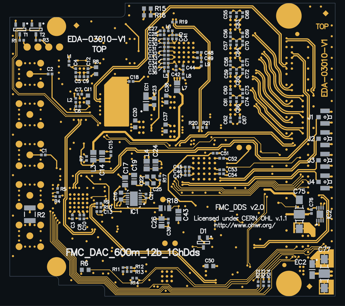
FMC DAC 600M 12B 1CHA DDS (OHWR0022 R1) is an open-hardware circuit board from the CERN Open Hardware Repository, designed in Altium Designer: a 4-layer board of 76.5 × 69 mm with 313 components and 252 nets, published under CERN-OHL-1.1.
review 80% walked · 18 findings: 1 blocker · 9 major · 8 minor (43 items)
Open in the interactive viewerRead the full review
Design review
Probe recorded 18 findings: 1 blocker · 9 major · 8 minor (43 items) on this design. Each is shown here with its reasoning; the full review links every one to the pins, nets and datasheet pages it rests on.
IC1 and IC14 are fixed 1.8 V LT1763-1.8 regulators feeding P2V5 and P3V3_DAC: the AD7980 VDD, the MAX5890 3.3 V supplies and the ADF4002 supplies all get 1.8 V
IC1 and IC14 are fixed 1.8 V LT1763-1.8 regulators feeding P2V5 and P3V3_DAC, so the AD7980 ADC core, the MAX5890 DAC's 3.3 V domains and the ADF4002 PLL all get 1.8 V, below their minimum supply.
The four regulators on sheet 2
All four are LT1763IDE-1.8#PBF, the fixed 1.8 V version, both in the BOM (manufacturer part number) and on the schematic symbol.
Regulator Input Output net Needs Status IC20 P1V8A 1.8 V correct IC15 P1V8D 1.8 V correct IC1 P3V3D P2V5 2.5 V 1.8 V fitted IC14 P5V0 P3V3_DAC 3.3 V 1.8 V fitted Where the 1.8 V goes
``
mermaid flowchart LR I1["IC1 LT1763-1.8"] -- "P2V5 at 1.8 V" --> A["IC19 AD7980<br/>VDD pin 2, VIO pin 10"] I14["IC14 LT1763-1.8"] -- "P3V3_DAC at 1.8 V" --> L7["L7 to AVDD33"] I14 --> L6["L6 to AVCLK"] I14 --> L8["L8 to DVDD33"] I14 --> L3["L3 to P3V3_PD"] L7 --> M["IC13 MAX5890 DAC"] L6 --> M L8 --> M L3 --> P["IC24 ADF4002 PLL"]``The numbers
Load Pins Specified supply Source AD7980 VDD IC19.2 2.375 / 2.5 / 2.625 V AD7980 datasheet, p.5 MAX5890 AVDD3.3 (via L7) IC13.14, .21, .22, .25, .26, .31, .32 3.135 to 3.465 V MAX5890 datasheet, p.5 MAX5890 AVCLK (via L6) IC13.36, .41 3.135 to 3.465 V statement MAX5890 DVDD3.3 (via L8) IC13.11 3.135 to 3.465 V MAX5890 datasheet, p.8 ADF4002 (via L3, P3V3_PD) IC24.7, .15, .16 2.7 to 3.3 V ADF4002 datasheet, p.6 LT1763 output options fixed 1.5, 1.8, 2.5, 3, 3.3, 5 V LT1763 datasheet, p.1 As ordered, the DAC, its clock input and the reference PLL are all below their minimum supply, and the ADC core runs at 1.8 V.
Why it matters and the fix
A fixed-output LT1763 cannot be trimmed: the SENSE pin only senses the output. The net names, the MAX5890 supply pin names and the sheet layout all show the intent was LT1763-2.5 for IC1 and LT1763-3.3 for IC14, so this is most likely a BOM and symbol error rather than a design intent.
Fix: order IC1 as LT1763IDE-2.5#PBF and IC14 as LT1763IDE-3.3#PBF (same DE-12 package and pinout) and correct the symbols. Boards already built to this BOM would need both parts replaced.
IC3 LM336-2.5 reference has its ADJ pin shorted to its anode (GND); it sets P2V5_VREF, the reference for both the AD7980 ADC and the AD5662 DAC
The LM336-2.5 reference IC3 has its ADJ pin shorted to its anode (GND), an undocumented configuration, and it sets P2V5_VREF, the reference for both the AD7980 ADC and the AD5662 DAC.
Where it is
``
mermaid flowchart LR S["P3V3_AD9516"] -- "R27 240 Ω" --> V["P2V5_VREF"] I["IC3 LM336M-2.5<br/>pin 8 CATHODE<br/>pins 4 ANODE and 5 ADJ on GND"] --- V V --> A["IC19 AD7980 ADC<br/>pin 1 REF"] V --> D["IC8 AD5662 DAC<br/>pin 2 reference"]``- IC3 (LM336M-2.5, SOIC-8): pin 4 ANODE and pin 5 ADJ both on GND, pin 8 CATHODE on P2V5_VREF.
- P2V5_VREF also carries C17, C78, C86, C108, and is biased by R27 240 Ω from P3V3_AD9516.
- Schematic sheet 8 'VCXO & PLL, WR Clock' draws ADJ and ANODE both to the ground symbol.
Why it is outside the datasheet
The TI datasheet describes the ADJ terminal as a trim input, one that 'allows the reference voltage and temperature coefficient to be trimmed easily' (LM336 datasheet, p.1). It is shown open or driven from a trim network across the device. Tying it straight to the anode is not a documented configuration, so the reference voltage and its temperature coefficient are not specified as wired.
The same circuit was found on SPEC TICKS (OHWR0045) as OBS-170.
Why it matters
Both converters take their full scale from this node, so an unspecified reference voltage becomes a gain error on the ADC and the DAC.
Suggested fix: leave ADJ unconnected (Figure 5 of the datasheet) or fit the documented trim network. The bias current, about (3.3 V - 2.5 V) / 240 Ω = 3.3 mA, is within the LM336's range.
- ReferencePlaneDiscontinuitymajorOpen
63 nets change reference between GND and P3V3D at 102 vias, none with a reference that continues across (fastest: DAC10_N at 100 ps 10-90 %, ASSUMED)
At 102 via(s), on 63 net(s), the signal leaves a layer referenced by one of GND and P3V3D for a layer referenced by the other, and no plane references both layers. Different nets: no via can carry the return across; only decoupling between the two planes near the via can. The capacitor carrying the return across was measured at each via, at the knee of the crossing net's edge against 50 ohm assumed: 102 with none. 102 of them at an ASSUMED edge (no edge on file for the net): state one (net_timing_state) and it is re-read. One decision covers the pair: whether GND and P3V3D are decoupled to each other near these vias. A via whose layers have more references than these two is a site of each pair it joins. None is partial: at every one, no reference continues across the via.
- 'NetD1_3' at (80.96, 91.28), TOP_LAYER -> BOTTOM_LAYER: GND on L2GND to P3V3D on L3PWR; pure, no reference continues across; stitching none, 51.7 mm of track past the via on BOTTOM_LAYER: At the 5 GHz knee of a 100 ps edge (100 ps 10-90 %, assumed: no edge is on file for the net) no capacitor carries the return; only the planes do. GND and P3V3D are not a thin pair (at most 0.2 mm), so their own capacitance does not carry the return. To serve it, change layers across the same plane, or move the signal to a layer referenced to ground. None.
- 'NetD1_3' at (119.22, 83.19), TOP_LAYER -> BOTTOM_LAYER: GND on L2GND to P3V3D on L3PWR; pure, no reference continues across; stitching none, 51.7 mm of track past the via on BOTTOM_LAYER: At the 5 GHz knee of a 100 ps edge (100 ps 10-90 %, assumed: no edge is on file for the net) no capacitor carries the return; only the planes do. GND and P3V3D are not a thin pair (at most 0.2 mm), so their own capacitance does not carry the return. To serve it, change layers across the same plane, or move the signal to a layer referenced to ground. None.
- 'PLL_SCLK' at (142.7, 80.78), TOP_LAYER -> BOTTOM_LAYER: GND on L2GND to P3V3D on L3PWR; pure, no reference continues across; stitching none, 41.7 mm of track past the via on BOTTOM_LAYER: At the 5 GHz knee of a 100 ps edge (1 ns 10-90 %, assumed: no edge is on file for the net) no capacitor carries the return; only the planes do. GND and P3V3D are not a thin pair (at most 0.2 mm), so their own capacitance does not carry the return. To serve it, change layers across the same plane, or move the signal to a layer referenced to ground. None.
- 'DELAY_IN' at (133.51, 75.25), TOP_LAYER -> BOTTOM_LAYER: GND on L2GND to P3V3D on L3PWR; pure, no reference continues across; stitching none, 34.9 mm of track past the via on BOTTOM_LAYER: At the 5 GHz knee of a 100 ps edge (100 ps 10-90 %, assumed: no edge is on file for the net) no capacitor carries the return; only the planes do. GND and P3V3D are not a thin pair (at most 0.2 mm), so their own capacitance does not carry the return. To serve it, change layers across the same plane, or move the signal to a layer referenced to ground. None.
- 'DELAY_IN' at (150.97, 82.87), TOP_LAYER -> BOTTOM_LAYER: GND on L2GND to P3V3D on L3PWR; pure, no reference continues across; stitching none, 34.9 mm of track past the via on BOTTOM_LAYER: At the 5 GHz knee of a 100 ps edge (100 ps 10-90 %, assumed: no edge is on file for the net) no capacitor carries the return; only the planes do. GND and P3V3D are not a thin pair (at most 0.2 mm), so their own capacitance does not carry the return. To serve it, change layers across the same plane, or move the signal to a layer referenced to ground. None.
- 'PLL1_CSB' at (144.15, 80.8), TOP_LAYER -> BOTTOM_LAYER: GND on L2GND to P3V3D on L3PWR; pure, no reference continues across; stitching none, 29.2 mm of track past the via on BOTTOM_LAYER: At the 5 GHz knee of a 100 ps edge (100 ps 10-90 %, assumed: no edge is on file for the net) no capacitor carries the return; only the planes do. GND and P3V3D are not a thin pair (at most 0.2 mm), so their own capacitance does not carry the return. To serve it, change layers across the same plane, or move the signal to a layer referenced to ground. None.
- 'PLL_SDIO' at (132.72, 78.42), TOP_LAYER -> BOTTOM_LAYER: GND on L2GND to P3V3D on L3PWR; pure, no reference continues across; stitching none, 27.8 mm of track past the via on BOTTOM_LAYER: At the 5 GHz knee of a 100 ps edge (100 ps 10-90 %, assumed: no edge is on file for the net) no capacitor carries the return; only the planes do. GND and P3V3D are not a thin pair (at most 0.2 mm), so their own capacitance does not carry the return. To serve it, change layers across the same plane, or move the signal to a layer referenced to ground. None.
- 'PLL_SDIO' at (135.89, 75.57), TOP_LAYER -> BOTTOM_LAYER: GND on L2GND to P3V3D on L3PWR; pure, no reference continues across; stitching none, 27.8 mm of track past the via on BOTTOM_LAYER: At the 5 GHz knee of a 100 ps edge (100 ps 10-90 %, assumed: no edge is on file for the net) no capacitor carries the return; only the planes do. GND and P3V3D are not a thin pair (at most 0.2 mm), so their own capacitance does not carry the return. To serve it, change layers across the same plane, or move the signal to a layer referenced to ground. None.
- 'PLL_SDIO' at (136.68, 94.93), TOP_LAYER -> BOTTOM_LAYER: GND on L2GND to P3V3D on L3PWR; pure, no reference continues across; stitching none, 27.8 mm of track past the via on BOTTOM_LAYER: At the 5 GHz knee of a 100 ps edge (100 ps 10-90 %, assumed: no edge is on file for the net) no capacitor carries the return; only the planes do. GND and P3V3D are not a thin pair (at most 0.2 mm), so their own capacitance does not carry the return. To serve it, change layers across the same plane, or move the signal to a layer referenced to ground. None.
- 'PLL1_SYNCB' at (150.5, 83.34), TOP_LAYER -> BOTTOM_LAYER: GND on L2GND to P3V3D on L3PWR; pure, no reference continues across; stitching none, 27.3 mm of track past the via on BOTTOM_LAYER: At the 5 GHz knee of a 100 ps edge (100 ps 10-90 %, assumed: no edge is on file for the net) no capacitor carries the return; only the planes do. GND and P3V3D are not a thin pair (at most 0.2 mm), so their own capacitance does not carry the return. To serve it, change layers across the same plane, or move the signal to a layer referenced to ground. None.
- 'PLL25DAC_DIN' at (139.38, 93.5), TOP_LAYER -> BOTTOM_LAYER: GND on L2GND to P3V3D on L3PWR; pure, no reference continues across; stitching none, 27.2 mm of track past the via on BOTTOM_LAYER: At the 5 GHz knee of a 100 ps edge (100 ps 10-90 %, assumed: no edge is on file for the net) no capacitor carries the return; only the planes do. GND and P3V3D are not a thin pair (at most 0.2 mm), so their own capacitance does not carry the return. To serve it, change layers across the same plane, or move the signal to a layer referenced to ground. None.
- 'PLL25DAC_DIN' at (143.99, 92.55), TOP_LAYER -> BOTTOM_LAYER: GND on L2GND to P3V3D on L3PWR; pure, no reference continues across; stitching none, 27.2 mm of track past the via on BOTTOM_LAYER: At the 5 GHz knee of a 100 ps edge (100 ps 10-90 %, assumed: no edge is on file for the net) no capacitor carries the return; only the planes do. GND and P3V3D are not a thin pair (at most 0.2 mm), so their own capacitance does not carry the return. To serve it, change layers across the same plane, or move the signal to a layer referenced to ground. None.
- and 90 more
Every site is a row of this finding's evidence, keyed by net, layers and position. GET /api/odb/boards/25/reference-planes?group=refchange%3AGND%7CP3V3D serves each with its own layer_image region; all of them lie in x 78.96..152.97, y 72.68..138.68 mm (board frame, Y up).
The reference on each layer is the first plane the track meets leaving the via, anti-pads and the net's own copper skipped. Whether it matters depends on each signal's edge rate, which nothing on file states for these nets: a slow static line crosses a split harmlessly, a fast edge does not.
At refchange:GND|P3V3D
- DecapOrdermajorOpen
DecapOrder: 5 findings (4 pins, 1 component)×5
Checked by the review, stands · Claude walker W3 (Cern session) — Checked: the distances are read from placement as stated. This is a layout-practice heuristic (Probe's starting thresholds); no datasheet on file fixes the order of these values at the 1-5 mm scale, where via and plane-spreading inductance usually dominate. Left for the owner.
At IC16, IC4.22, IC5.22, IC6.22, IC9.1
Each finding, with its own headline
IC16IC16 supply pins 18, 19, 22 on 'P3V3D': the smallest capacitor C101 sits 2.9 mm away, behind C106 at 1.2 mm
IC16 supply pins 18, 19, 22 on 'P3V3D': the smallest capacitor C101 sits 2.9 mm away, behind C106 at 1.2 mm. IC16.18: the smallest value, C101 (10 nF), is 2.9 mm from the pin and C106 (100 nF) 1.2 mm: the high-frequency part sits behind more inductance than the bulk part, which needs it least. IC16.19: the smallest value, C101 (10 nF), is 3.3 mm from the pin and C106 (100 nF) 1.3 mm: the high-frequency part sits behind more inductance than the bulk part, which needs it least. IC16.22: the smallest value, C101 (10 nF), is 4.7 mm from the pin and C105 (100 nF) 1.5 mm: the high-frequency part sits behind more inductance than the bulk part, which needs it least. Swap them, or bring the smallest value to the pin: it serves the fastest current and is the one the loop inductance defeats. Distances are pad centre to pin centre in the board plane. The 5 mm radius, the 10x value step and the 1 mm / 1.5x tie tolerance are Probe's starting values.
IC4.22IC4 supply pin 22 on 'P3V3_BUF': the smallest capacitor C64 sits 1.7 mm away, behind C56 at 0.5 mm
IC4 supply pin 22 on 'P3V3_BUF': the smallest capacitor C64 sits 1.7 mm away, behind C56 at 0.5 mm. IC4.22: the smallest value, C64 (10 nF), is 1.7 mm from the pin and C56 (100 nF) 0.5 mm: the high-frequency part sits behind more inductance than the bulk part, which needs it least. Swap them, or bring the smallest value to the pin: it serves the fastest current and is the one the loop inductance defeats. Distances are pad centre to pin centre in the board plane. The 5 mm radius, the 10x value step and the 1 mm / 1.5x tie tolerance are Probe's starting values.
IC5.22IC5 supply pin 22 on 'P3V3_BUF': the smallest capacitor C65 sits 1.7 mm away, behind C58 at 0.5 mm
IC5 supply pin 22 on 'P3V3_BUF': the smallest capacitor C65 sits 1.7 mm away, behind C58 at 0.5 mm. IC5.22: the smallest value, C65 (10 nF), is 1.7 mm from the pin and C58 (100 nF) 0.5 mm: the high-frequency part sits behind more inductance than the bulk part, which needs it least. Swap them, or bring the smallest value to the pin: it serves the fastest current and is the one the loop inductance defeats. Distances are pad centre to pin centre in the board plane. The 5 mm radius, the 10x value step and the 1 mm / 1.5x tie tolerance are Probe's starting values.
IC6.22IC6 supply pin 22 on 'P3V3_BUF': the smallest capacitor C66 sits 1.7 mm away, behind C60 at 0.5 mm
IC6 supply pin 22 on 'P3V3_BUF': the smallest capacitor C66 sits 1.7 mm away, behind C60 at 0.5 mm. IC6.22: the smallest value, C66 (10 nF), is 1.7 mm from the pin and C60 (100 nF) 0.5 mm: the high-frequency part sits behind more inductance than the bulk part, which needs it least. Swap them, or bring the smallest value to the pin: it serves the fastest current and is the one the loop inductance defeats. Distances are pad centre to pin centre in the board plane. The 5 mm radius, the 10x value step and the 1 mm / 1.5x tie tolerance are Probe's starting values.
IC9.1IC9 supply pin 1 on 'P3V3_AD9516': the smallest capacitor C54 sits 5.0 mm away, behind C52 at 1.3 mm
IC9 supply pin 1 on 'P3V3_AD9516': the smallest capacitor C54 sits 5.0 mm away, behind C52 at 1.3 mm. IC9.1: the smallest value, C54 (10 nF), is 5.0 mm from the pin and C52 (100 nF) 1.3 mm: the high-frequency part sits behind more inductance than the bulk part, which needs it least. Swap them, or bring the smallest value to the pin: it serves the fastest current and is the one the loop inductance defeats. Distances are pad centre to pin centre in the board plane. The 5 mm radius, the 10x value step and the 1 mm / 1.5x tie tolerance are Probe's starting values.
- DecapViaFanoutmajorOpen
DecapViaFanout: 4 components×4
Checked by the review, stands · Claude walker W3 (Cern session) — Checked: the fan-out length is read from the copper as stated. The 0.5 nH limit is Probe's starting value, not a datasheet or vendor requirement on file; whether it matters depends on this capacitor's role in the rail's PDN target. Left for the owner.
At C116, C18, C29, C31
Each finding, with its own headline
C116C116 on 'P3V3D': its rail pad reaches its via over 0.84 mm of track and its ground pad over 3.17 mm, adding about 1.10 nH to its loop, past Probe's 0.5 nH starting value; put the vias at the pads
C116 on 'P3V3D': its rail pad reaches its via over 0.84 mm of track and its ground pad over 3.17 mm, adding about 1.10 nH to its loop, past Probe's 0.5 nH starting value; put the vias at the pads. C116.1 (rail) runs 0.84 mm along its copper to its nearest via, beside the pad; C116.2 (ground) runs 3.17 mm along its copper to its nearest via, 2.17 mm past the 1 mm beside the pad: 1.10 nH. Each run past the pad as one conductor of a pair 1.60 mm apart (the pad pitch), 0.2 l ln(D/R) nH with R 0.127 mm (the track's width is not read): 1.10 nH in all. Put the vias at the pads (or in them), one per pad at least, the rail's and the ground's close together; the capacitor's own inductance as mounted is 1.27 nH (pad 0.10 nH + no via of the second net within 1 mm of its pad: the study's 0.6 nH per mm of 1.10 mm depth, ASSUMED). 0.5 nH is Probe's starting value, about the whole mounted inductance of a well-mounted 0402.
C18C18 on 'P5V0': its ground pad over 3.03 mm, adding about 0.80 nH to its loop, past Probe's 0.5 nH starting value; put the vias at the pads
C18 on 'P5V0': its ground pad over 3.03 mm, adding about 0.80 nH to its loop, past Probe's 0.5 nH starting value; put the vias at the pads. C18.2 (rail) not measured: the pad sits in a pour of its net on its own layer, which has no track length to measure; C18.1 (ground) runs 3.03 mm along its copper to its nearest via, 2.03 mm past the 1 mm beside the pad: 0.80 nH. Each run past the pad as one conductor of a pair 0.90 mm apart (the pad pitch), 0.2 l ln(D/R) nH with R 0.127 mm (the track's width is not read): 0.80 nH in all. Put the vias at the pads (or in them), one per pad at least, the rail's and the ground's close together; the capacitor's own inductance as mounted is 1.03 nH (pad 0.07 nH + no via of the second net within 1 mm of its pad: the study's 0.6 nH per mm of 1.10 mm depth, ASSUMED). 0.5 nH is Probe's starting value, about the whole mounted inductance of a well-mounted 0402.
C29C29 on 'AVDD33': its rail pad reaches its via over 1.49 mm of track and its ground pad over 2.41 mm, adding about 0.74 nH to its loop, past Probe's 0.5 nH starting value; put the vias at the pads
C29 on 'AVDD33': its rail pad reaches its via over 1.49 mm of track and its ground pad over 2.41 mm, adding about 0.74 nH to its loop, past Probe's 0.5 nH starting value; put the vias at the pads. C29.2 (rail) runs 1.49 mm along its copper to its nearest via, 0.49 mm past the 1 mm beside the pad: 0.19 nH; C29.1 (ground) runs 2.41 mm along its copper to its nearest via, 1.41 mm past the 1 mm beside the pad: 0.55 nH. Each run past the pad as one conductor of a pair 0.90 mm apart (the pad pitch), 0.2 l ln(D/R) nH with R 0.127 mm (the track's width is not read): 0.74 nH in all. Put the vias at the pads (or in them), one per pad at least, the rail's and the ground's close together; the capacitor's own inductance as mounted is 1.03 nH (pad 0.07 nH + no via of the first net within 1 mm of its pad: the study's 0.6 nH per mm of 1.10 mm depth, ASSUMED). 0.5 nH is Probe's starting value, about the whole mounted inductance of a well-mounted 0402.
C31C31 on 'AVDD33': its rail pad reaches its via over 2.45 mm of track and its ground pad over 1.52 mm, adding about 0.77 nH to its loop, past Probe's 0.5 nH starting value; put the vias at the pads
C31 on 'AVDD33': its rail pad reaches its via over 2.45 mm of track and its ground pad over 1.52 mm, adding about 0.77 nH to its loop, past Probe's 0.5 nH starting value; put the vias at the pads. C31.2 (rail) runs 2.45 mm along its copper to its nearest via, 1.45 mm past the 1 mm beside the pad: 0.57 nH; C31.1 (ground) runs 1.52 mm along its copper to its nearest via, 0.52 mm past the 1 mm beside the pad: 0.20 nH. Each run past the pad as one conductor of a pair 0.90 mm apart (the pad pitch), 0.2 l ln(D/R) nH with R 0.127 mm (the track's width is not read): 0.77 nH in all. Put the vias at the pads (or in them), one per pad at least, the rail's and the ground's close together; the capacitor's own inductance as mounted is 1.03 nH (pad 0.07 nH + no via of the first net within 1 mm of its pad: the study's 0.6 nH per mm of 1.10 mm depth, ASSUMED). 0.5 nH is Probe's starting value, about the whole mounted inductance of a well-mounted 0402.
- EsdProtectorPlacementmajorOpen
EsdProtectorPlacement: 2 components×2
Checked by the review, stands · Claude walker W3 (Cern session) — Checked: the via count and distance are read from the copper as stated. Placement guidance for the protector is layout practice; no datasheet requirement on file for this part sets a distance limit. Left for the owner.
At D1, D2
Each finding, with its own headline
D1D1.3 on 'NetD1_3': 1 via(s) between J9.1 and D1.3
D1 (BAR66) protects 'NetD1_3' at J9.1. Along the copper: 51.23 mm of track from the contact, 1 via(s) before it, on a 47.26 mm branch off the line; the line runs 4.99 mm on to R2.2; D1 sits 36.92 mm farther from the contact than the nearest place outside J9.
1 via(s) between J9.1 and D1.3: the strike reaches an inner layer before it is clamped. D1.3 hangs 47.26 mm off the line (limit 1 mm, default: no datasheet figure on file): the line carries the strike past it while the clamp is reached through the branch.
Measured on the copper the ODB states: tracks, the pads they land on, and the netlist's vias. Not a straight line between centroids.
D2D2.3 on 'NetD2_3': D2.3 hangs 3.84 mm off the line (limit 1 mm, default
D2 (BAR66) protects 'NetD2_3' at J10.1. Along the copper: 16.16 mm of track from the contact, 0 via(s) before it, on a 3.84 mm branch off the line; the line runs 13.35 mm on to IC25.8; D2 sits 9.28 mm farther from the contact than the nearest place outside J10.
D2.3 hangs 3.84 mm off the line (limit 1 mm, default: no datasheet figure on file): the line carries the strike past it while the clamp is reached through the branch. D2 joins the line 12.32 mm from J10.1 on a 13.35 mm run to IC25.8: nearer the far end than the contact, so the surge travels most of the line before it is clamped.
Measured on the copper the ODB states: tracks, the pads they land on, and the netlist's vias. Not a straight line between centroids.
- PartLifecyclemajorOpen
PartLifecycle: 2 part numbers×2
1 Last Time Buy, 1 Obsolete · on 4 placements
At C75, D1
Each finding, with its own headline
C75NFE61PT102E1H9L on 2 placements (C75, C77): the distributor catalogue reports "Last Time Buy" for Murata Electronics's NFE61PT102E1H9L
NFE61PT102E1H9L on 2 placements (C75, C77): the distributor catalogue reports "Last Time Buy" for Murata Electronics's NFE61PT102E1H9L — a sourcing/longevity risk to confirm against the MANUFACTURER before acting. That is the maker this board's BOM names (MURATA). A distributor delisting is not the same claim as the part being unavailable; check the vendor's own lifecycle/product-change notice for the status and any named successor. Re-read the source: GET /api/odb/parts/NFE61PT102E1H9L/providers (which provider said it, the maker and part number it matched, its own words, and when we asked). LAST BUY 2027-09-30 — 319 day(s) remaining to place a final order. The distributor reports NONE left. No approved alternate is recorded for this position.
D1BAR66 on 2 placements (D1, D2): the distributor catalogue reports "Obsolete" for Infineon Technologies's BAR66
BAR66 on 2 placements (D1, D2): the distributor catalogue reports "Obsolete" for Infineon Technologies's BAR66 — a sourcing/longevity risk to confirm against the MANUFACTURER before acting. That is the maker this board's BOM names (INFINEON). A distributor delisting is not the same claim as the part being unavailable; check the vendor's own lifecycle/product-change notice for the status and any named successor. Re-read the source: GET /api/odb/parts/BAR66/providers (which provider said it, the maker and part number it matched, its own words, and when we asked). No approved alternate is recorded for this position.
- PartLifecyclemajorOpen
PartLifecycle: 2 part numbers×2
1 Obsolete, 1 Discontinued at DigiKey · on 2 placements
At IC11, IC18
Each finding, with its own headline
IC11LP5951MF-3.0/NOPB on IC11: the distributor catalogue reports "Obsolete" for National Semiconductor's LP5951MF-3.0/NOPB
LP5951MF-3.0/NOPB on IC11: the distributor catalogue reports "Obsolete" for National Semiconductor's LP5951MF-3.0/NOPB — a sourcing/longevity risk to confirm against the MANUFACTURER before acting. That is the maker this board's BOM names (NATIONAL SEMICONDUCTOR). A distributor delisting is not the same claim as the part being unavailable; check the vendor's own lifecycle/product-change notice for the status and any named successor. Re-read the source: GET /api/odb/parts/LP5951MF-3.0/NOPB/providers (which provider said it, the maker and part number it matched, its own words, and when we asked). No approved alternate is recorded for this position.
IC18SN74LVC244ADBRG4 on IC18: the distributor catalogue reports "Discontinued at DigiKey" for Texas Instruments's SN74LVC244ADBRG4
SN74LVC244ADBRG4 on IC18: the distributor catalogue reports "Discontinued at DigiKey" for Texas Instruments's SN74LVC244ADBRG4 — a sourcing/longevity risk to confirm against the MANUFACTURER before acting. That is the maker this board's BOM names (TEXAS INSTRUMENTS). A distributor delisting is not the same claim as the part being unavailable; check the vendor's own lifecycle/product-change notice for the status and any named successor. Re-read the source: GET /api/odb/parts/SN74LVC244ADBRG4/providers (which provider said it, the maker and part number it matched, its own words, and when we asked). No approved alternate is recorded for this position.
- ReferencePlaneDiscontinuitymajorOpen
ReferencePlaneDiscontinuity: 10 boards×10
Checked by the review, stands · Claude walker W3 (Cern session) — Checked: the reference break is read from the copper as stated. Whether it matters depends on the signal's edge rate and the receiver's margin, which no datasheet or app note on file fixes for this net; the impedance step and reflection figures are Probe's model, and the thresholds are its starting values. Layout practice, not a datasheet requirement. Left for the owner.
At gap:L3PWR:hole 87.95,94.46|88.26,96.51, refchange:GND|P3V3_AD9510, refchange:GND|P3V3_AD9516, refchange:GND|P5V0, split@L3PWR:AVDD18|AVDD33, split@L3PWR:AVDD33|P5V0 and 4 more
Each finding, with its own headline
gap:L3PWR:hole 87.95,94.46|88.26,96.51'CLK_PD' crosses one gap in L3PWR's negative-plane field at 1 place, the longest 0.03 mm (fastest: CLK_PD at 1 ns 10-90 %, suggested by its name)
Along 'CLK_PD' on BOTTOM_LAYER, L3PWR is a negative layer (copper everywhere inside the profile), and its field is cleared for 0.03 mm under the track at (87.97, 95.7). The layer does not state the nets either side, so whether this is a split between two planes or a void in one is not said; either way the return current has to go round it. What cleared it: the hole at x 87.95..88.26, y 94.46..96.51. One decision covers the void: whether these tracks may cross it, or the plane should be filled under them. No crossing has a plane on the track's other side, so the whole return meets the break.
- 'CLK_PD' on BOTTOM_LAYER at (87.97, 95.7), 0.03 mm; other side: none: the signal layer is outermost
Every site is a row of this finding's evidence, keyed by net, layers and position. GET /api/odb/boards/25/reference-planes?group=gap%3AL3PWR%3Ahole%2087.95%2C94.46%7C88.26%2C96.51 serves each with its own layer_image region; all of them lie in x 86.95..88.99, y 94.7..96.7 mm (board frame, Y up).
Read from the copper as drawn on the reference layer, along each track's centreline at exact breakpoints. The reference is the copper beside the track, never the layer's type or name. Whether it matters depends on each signal's edge rate, which nothing on file states for these nets: a slow static line crosses a split harmlessly, a fast edge does not.
refchange:GND|P3V3_AD951014 nets change reference between GND and P3V3_AD9510 at 15 vias, none with a reference that continues across (fastest: NetC115_2 at 100 ps 10-90 %, ASSUMED)
At 15 via(s), on 14 net(s), the signal leaves a layer referenced by one of GND and P3V3_AD9510 for a layer referenced by the other, and no plane references both layers. Different nets: no via can carry the return across; only decoupling between the two planes near the via can. The capacitor carrying the return across was measured at each via, at the knee of the crossing net's edge against 50 ohm assumed: 15 with none. 15 of them at an ASSUMED edge (no edge on file for the net): state one (net_timing_state) and it is re-read. One decision covers the pair: whether GND and P3V3_AD9510 are decoupled to each other near these vias. A via whose layers have more references than these two is a site of each pair it joins. None is partial: at every one, no reference continues across the via.
- 'PLL_SCLK' at (87.06, 89.94), TOP_LAYER -> BOTTOM_LAYER: GND on L2GND to P3V3_AD9510 on L3PWR; pure, no reference continues across; stitching none, 41.7 mm of track past the via on BOTTOM_LAYER: At the 5 GHz knee of a 100 ps edge (1 ns 10-90 %, assumed: no edge is on file for the net) no capacitor carries the return; only the planes do. GND and P3V3_AD9510 are not a thin pair (at most 0.2 mm), so their own capacitance does not carry the return. To serve it, change layers across the same plane, or move the signal to a layer referenced to ground. Measured for reference: C148 (100 nF 0402) 2.9 mm away: 1.00 nH in the 0.800 mm cavity + 0.30 nH ESL + 1.21 nH mounting (pad 0.07 nH (vias beside the pads) + 1 via pair(s) at 1.33 mm pitch, 0.20 mm drill, 1.10 mm to the farther plane): 78.8 ohm at the knee, 158 % of 50 ohm (assumed track impedance). None.
- 'PLL1_CSB' at (85.77, 91.49), TOP_LAYER -> BOTTOM_LAYER: GND on L2GND to P3V3_AD9510 on L3PWR; pure, no reference continues across; stitching none, 29.2 mm of track past the via on BOTTOM_LAYER: At the 5 GHz knee of a 100 ps edge (100 ps 10-90 %, assumed: no edge is on file for the net) no capacitor carries the return; only the planes do. GND and P3V3_AD9510 are not a thin pair (at most 0.2 mm), so their own capacitance does not carry the return. To serve it, change layers across the same plane, or move the signal to a layer referenced to ground. Measured for reference: C148 (100 nF 0402) 1.5 mm away: 0.79 nH in the 0.800 mm cavity + 0.30 nH ESL + 1.21 nH mounting (pad 0.07 nH (vias beside the pads) + 1 via pair(s) at 1.33 mm pitch, 0.20 mm drill, 1.10 mm to the farther plane): 72.3 ohm at the knee, 145 % of 50 ohm (assumed track impedance). None.
- 'PLL1_SYNCB' at (87.94, 88.86), TOP_LAYER -> BOTTOM_LAYER: GND on L2GND to P3V3_AD9510 on L3PWR; pure, no reference continues across; stitching none, 27.3 mm of track past the via on BOTTOM_LAYER: At the 5 GHz knee of a 100 ps edge (100 ps 10-90 %, assumed: no edge is on file for the net) no capacitor carries the return; only the planes do. GND and P3V3_AD9510 are not a thin pair (at most 0.2 mm), so their own capacitance does not carry the return. To serve it, change layers across the same plane, or move the signal to a layer referenced to ground. None.
- 'NetC115_2' at (95.45, 94.72), TOP_LAYER -> BOTTOM_LAYER: GND on L2GND to P3V3_AD9510 on L3PWR; pure, no reference continues across; stitching none, 11.7 mm of track past the via on BOTTOM_LAYER: At the 5 GHz knee of a 100 ps edge (100 ps 10-90 %, assumed: no edge is on file for the net) no capacitor carries the return; only the planes do. GND and P3V3_AD9510 are not a thin pair (at most 0.2 mm), so their own capacitance does not carry the return. To serve it, change layers across the same plane, or move the signal to a layer referenced to ground. None.
- 'NetC115_2' at (98.75, 95.07), TOP_LAYER -> BOTTOM_LAYER: GND on L2GND to P3V3_AD9510 on L3PWR; pure, no reference continues across; stitching none, 11.7 mm of track past the via on BOTTOM_LAYER: At the 5 GHz knee of a 100 ps edge (100 ps 10-90 %, assumed: no edge is on file for the net) no capacitor carries the return; only the planes do. GND and P3V3_AD9510 are not a thin pair (at most 0.2 mm), so their own capacitance does not carry the return. To serve it, change layers across the same plane, or move the signal to a layer referenced to ground. Measured for reference: C119 (100 nF 0402) 1.4 mm away: 0.78 nH in the 0.800 mm cavity + 0.30 nH ESL + 0.73 nH mounting (pad 0.07 nH + no via of the second net within 1 mm of its pad: the study's 0.6 nH per mm of 1.10 mm depth, ASSUMED): 56.8 ohm at the knee, 114 % of 50 ohm (assumed track impedance). None.
- 'CLK_P' at (96.13, 92.62), TOP_LAYER -> BOTTOM_LAYER: GND on L2GND to P3V3_AD9510 on L3PWR; pure, no reference continues across; stitching none, 4.1 mm of track past the via on BOTTOM_LAYER: At the 5 GHz knee of a 100 ps edge (1 ns 10-90 %, assumed: no edge is on file for the net) no capacitor carries the return; only the planes do. GND and P3V3_AD9510 are not a thin pair (at most 0.2 mm), so their own capacitance does not carry the return. To serve it, change layers across the same plane, or move the signal to a layer referenced to ground. Measured for reference: C13 (100 nF 0402) 1.6 mm away: 0.80 nH in the 0.800 mm cavity + 0.30 nH ESL + 0.73 nH mounting (pad 0.07 nH + no via of the first net within 1 mm of its pad: the study's 0.6 nH per mm of 1.10 mm depth, ASSUMED): 57.6 ohm at the knee, 115 % of 50 ohm (assumed track impedance). None.
- 'CLK_N' at (96.13, 93.28), TOP_LAYER -> BOTTOM_LAYER: GND on L2GND to P3V3_AD9510 on L3PWR; pure, no reference continues across; stitching none, 4.0 mm of track past the via on BOTTOM_LAYER: At the 5 GHz knee of a 100 ps edge (1 ns 10-90 %, assumed: no edge is on file for the net) no capacitor carries the return; only the planes do. GND and P3V3_AD9510 are not a thin pair (at most 0.2 mm), so their own capacitance does not carry the return. To serve it, change layers across the same plane, or move the signal to a layer referenced to ground. Measured for reference: C13 (100 nF 0402) 2.1 mm away: 0.90 nH in the 0.800 mm cavity + 0.30 nH ESL + 0.73 nH mounting (pad 0.07 nH + no via of the first net within 1 mm of its pad: the study's 0.6 nH per mm of 1.10 mm depth, ASSUMED): 60.6 ohm at the knee, 121 % of 50 ohm (assumed track impedance). None.
- 'REFINC_P' at (96.26, 87.25), TOP_LAYER -> BOTTOM_LAYER: GND on L2GND to P3V3_AD9510 on L3PWR; pure, no reference continues across; stitching none, 2.8 mm of track past the via on BOTTOM_LAYER: At the 5 GHz knee of a 100 ps edge (100 ps 10-90 %, assumed: no edge is on file for the net) no capacitor carries the return; only the planes do. GND and P3V3_AD9510 are not a thin pair (at most 0.2 mm), so their own capacitance does not carry the return. To serve it, change layers across the same plane, or move the signal to a layer referenced to ground. None.
- 'REFINC_N' at (95.61, 87.25), TOP_LAYER -> BOTTOM_LAYER: GND on L2GND to P3V3_AD9510 on L3PWR; pure, no reference continues across; stitching none, 2.6 mm of track past the via on BOTTOM_LAYER: At the 5 GHz knee of a 100 ps edge (100 ps 10-90 %, assumed: no edge is on file for the net) no capacitor carries the return; only the planes do. GND and P3V3_AD9510 are not a thin pair (at most 0.2 mm), so their own capacitance does not carry the return. To serve it, change layers across the same plane, or move the signal to a layer referenced to ground. None.
- 'CLK2OUT_N' at (91.11, 97.03), TOP_LAYER -> BOTTOM_LAYER: GND on L2GND to P3V3_AD9510 on L3PWR; pure, no reference continues across; stitching none, 1.8 mm of track past the via on BOTTOM_LAYER: At the 5 GHz knee of a 100 ps edge (1 ns 10-90 %, assumed: no edge is on file for the net) no capacitor carries the return; only the planes do. GND and P3V3_AD9510 are not a thin pair (at most 0.2 mm), so their own capacitance does not carry the return. To serve it, change layers across the same plane, or move the signal to a layer referenced to ground. Measured for reference: C140 (100 nF 0402) 2.4 mm away: 0.94 nH in the 0.800 mm cavity + 0.30 nH ESL + 0.73 nH mounting (pad 0.07 nH + no via of the second net within 1 mm of its pad: the study's 0.6 nH per mm of 1.10 mm depth, ASSUMED): 62.0 ohm at the knee, 124 % of 50 ohm (assumed track impedance). None.
- 'CLK2OUT_P' at (91.76, 97.03), TOP_LAYER -> BOTTOM_LAYER: GND on L2GND to P3V3_AD9510 on L3PWR; pure, no reference continues across; stitching none, 1.8 mm of track past the via on BOTTOM_LAYER: At the 5 GHz knee of a 100 ps edge (1 ns 10-90 %, assumed: no edge is on file for the net) no capacitor carries the return; only the planes do. GND and P3V3_AD9510 are not a thin pair (at most 0.2 mm), so their own capacitance does not carry the return. To serve it, change layers across the same plane, or move the signal to a layer referenced to ground. Measured for reference: C133 (100 nF 0402) 2.5 mm away: 0.95 nH in the 0.800 mm cavity + 0.30 nH ESL + 0.73 nH mounting (pad 0.07 nH + no via of the second net within 1 mm of its pad: the study's 0.6 nH per mm of 1.10 mm depth, ASSUMED): 62.1 ohm at the knee, 124 % of 50 ohm (assumed track impedance). None.
- 'NetIC26_20' at (86.4, 91.19), TOP_LAYER -> BOTTOM_LAYER: GND on L2GND to P3V3_AD9510 on L3PWR; pure, no reference continues across; stitching none, 1.6 mm of track past the via on BOTTOM_LAYER: At the 5 GHz knee of a 100 ps edge (100 ps 10-90 %, assumed: no edge is on file for the net) no capacitor carries the return; only the planes do. GND and P3V3_AD9510 are not a thin pair (at most 0.2 mm), so their own capacitance does not carry the return. To serve it, change layers across the same plane, or move the signal to a layer referenced to ground. Measured for reference: C148 (100 nF 0402) 1.6 mm away: 0.81 nH in the 0.800 mm cavity + 0.30 nH ESL + 1.21 nH mounting (pad 0.07 nH (vias beside the pads) + 1 via pair(s) at 1.33 mm pitch, 0.20 mm drill, 1.10 mm to the farther plane): 72.9 ohm at the knee, 146 % of 50 ohm (assumed track impedance). None.
- and 3 more
Every site is a row of this finding's evidence, keyed by net, layers and position. GET /api/odb/boards/25/reference-planes?group=refchange%3AGND%7CP3V3_AD9510 serves each with its own layer_image region; all of them lie in x 83.77..100.75, y 85.25..99.03 mm (board frame, Y up).
The reference on each layer is the first plane the track meets leaving the via, anti-pads and the net's own copper skipped. Whether it matters depends on each signal's edge rate, which nothing on file states for these nets: a slow static line crosses a split harmlessly, a fast edge does not.
refchange:GND|P3V3_AD951616 nets change reference between GND and P3V3_AD9516 at 16 vias, none with a reference that continues across (fastest: 25M_VCXO at 100 ps 10-90 %, ASSUMED)
At 16 via(s), on 16 net(s), the signal leaves a layer referenced by one of GND and P3V3_AD9516 for a layer referenced by the other, and no plane references both layers. Different nets: no via can carry the return across; only decoupling between the two planes near the via can. The capacitor carrying the return across was measured at each via, at the knee of the crossing net's edge against 50 ohm assumed: 16 with none. 16 of them at an ASSUMED edge (no edge on file for the net): state one (net_timing_state) and it is re-read. One decision covers the pair: whether GND and P3V3_AD9516 are decoupled to each other near these vias. A via whose layers have more references than these two is a site of each pair it joins. None is partial: at every one, no reference continues across the via.
- 'CLK1OUT_P' at (116.21, 107), TOP_LAYER -> BOTTOM_LAYER: GND on L2GND to P3V3_AD9516 on L3PWR; pure, no reference continues across; stitching none, 21.8 mm of track past the via on BOTTOM_LAYER: At the 5 GHz knee of a 100 ps edge (1 ns 10-90 %, assumed: no edge is on file for the net) no capacitor carries the return; only the planes do. GND and P3V3_AD9516 are not a thin pair (at most 0.2 mm), so their own capacitance does not carry the return. To serve it, change layers across the same plane, or move the signal to a layer referenced to ground. Measured for reference: C94 (100 nF 0402) 2.1 mm away: 0.90 nH in the 0.800 mm cavity + 0.30 nH ESL + 1.01 nH mounting (pad 0.07 nH (vias beside the pads) + 1 via pair(s) at 0.84 mm pitch, 0.20 mm drill, 1.10 mm to the farther plane): 69.5 ohm at the knee, 139 % of 50 ohm (assumed track impedance). None.
- 'CLK1OUT_N' at (115.25, 107), TOP_LAYER -> BOTTOM_LAYER: GND on L2GND to P3V3_AD9516 on L3PWR; pure, no reference continues across; stitching none, 21.5 mm of track past the via on BOTTOM_LAYER: At the 5 GHz knee of a 100 ps edge (1 ns 10-90 %, assumed: no edge is on file for the net) no capacitor carries the return; only the planes do. GND and P3V3_AD9516 are not a thin pair (at most 0.2 mm), so their own capacitance does not carry the return. To serve it, change layers across the same plane, or move the signal to a layer referenced to ground. None.
- 'PLL25DAC_SCLK' at (129.74, 89.53), TOP_LAYER -> BOTTOM_LAYER: GND on L2GND to P3V3_AD9516 on L3PWR; pure, no reference continues across; stitching none, 14.7 mm of track past the via on BOTTOM_LAYER: At the 5 GHz knee of a 100 ps edge (1 ns 10-90 %, assumed: no edge is on file for the net) no capacitor carries the return; only the planes do. GND and P3V3_AD9516 are not a thin pair (at most 0.2 mm), so their own capacitance does not carry the return. To serve it, change layers across the same plane, or move the signal to a layer referenced to ground. None.
- 'PLL2_LD' at (135.26, 105.57), TOP_LAYER -> BOTTOM_LAYER: GND on L2GND to P3V3_AD9516 on L3PWR; pure, no reference continues across; stitching none, 12.2 mm of track past the via on BOTTOM_LAYER: At the 5 GHz knee of a 100 ps edge (100 ps 10-90 %, assumed: no edge is on file for the net) no capacitor carries the return; only the planes do. GND and P3V3_AD9516 are not a thin pair (at most 0.2 mm), so their own capacitance does not carry the return. To serve it, change layers across the same plane, or move the signal to a layer referenced to ground. None.
- 'NetC53_2' at (127.32, 100.8), TOP_LAYER -> BOTTOM_LAYER: GND on L2GND to P3V3_AD9516 on L3PWR; pure, no reference continues across; stitching none, 8.0 mm of track past the via on BOTTOM_LAYER: At the 5 GHz knee of a 100 ps edge (100 ps 10-90 %, assumed: no edge is on file for the net) no capacitor carries the return; only the planes do. GND and P3V3_AD9516 are not a thin pair (at most 0.2 mm), so their own capacitance does not carry the return. To serve it, change layers across the same plane, or move the signal to a layer referenced to ground. Measured for reference: C54 (10 nF 0402) 1.4 mm away: 0.76 nH in the 0.800 mm cavity + 0.30 nH ESL + 0.73 nH mounting (pad 0.07 nH + no via of the first net within 1 mm of its pad: the study's 0.6 nH per mm of 1.10 mm depth, ASSUMED): 56.2 ohm at the knee, 112 % of 50 ohm (assumed track impedance). None.
- 'PLL2_SYNC_N' at (127.32, 101.92), TOP_LAYER -> BOTTOM_LAYER: GND on L2GND to P3V3_AD9516 on L3PWR; pure, no reference continues across; stitching none, 7.7 mm of track past the via on BOTTOM_LAYER: At the 5 GHz knee of a 100 ps edge (100 ps 10-90 %, assumed: no edge is on file for the net) no capacitor carries the return; only the planes do. GND and P3V3_AD9516 are not a thin pair (at most 0.2 mm), so their own capacitance does not carry the return. To serve it, change layers across the same plane, or move the signal to a layer referenced to ground. Measured for reference: C54 (10 nF 0402) 2.0 mm away: 0.89 nH in the 0.800 mm cavity + 0.30 nH ESL + 0.73 nH mounting (pad 0.07 nH + no via of the first net within 1 mm of its pad: the study's 0.6 nH per mm of 1.10 mm depth, ASSUMED): 60.2 ohm at the knee, 120 % of 50 ohm (assumed track impedance). None.
- 'DAC_CLK_N' at (120.72, 110.36), TOP_LAYER -> BOTTOM_LAYER: GND on L2GND to P3V3_AD9516 on L3PWR; pure, no reference continues across; stitching none, 5.3 mm of track past the via on BOTTOM_LAYER: At the 5 GHz knee of a 100 ps edge (1 ns 10-90 %, assumed: no edge is on file for the net) no capacitor carries the return; only the planes do. GND and P3V3_AD9516 are not a thin pair (at most 0.2 mm), so their own capacitance does not carry the return. To serve it, change layers across the same plane, or move the signal to a layer referenced to ground. Measured for reference: C92 (100 nF 0402) 2.8 mm away: 0.99 nH in the 0.800 mm cavity + 0.30 nH ESL + 1.02 nH mounting (pad 0.07 nH (vias beside the pads) + 1 via pair(s) at 0.87 mm pitch, 0.20 mm drill, 1.10 mm to the farther plane): 72.5 ohm at the knee, 145 % of 50 ohm (assumed track impedance). None.
- 'DAC_CLK_P' at (121.38, 110.36), TOP_LAYER -> BOTTOM_LAYER: GND on L2GND to P3V3_AD9516 on L3PWR; pure, no reference continues across; stitching none, 5.3 mm of track past the via on BOTTOM_LAYER: At the 5 GHz knee of a 100 ps edge (1 ns 10-90 %, assumed: no edge is on file for the net) no capacitor carries the return; only the planes do. GND and P3V3_AD9516 are not a thin pair (at most 0.2 mm), so their own capacitance does not carry the return. To serve it, change layers across the same plane, or move the signal to a layer referenced to ground. None.
- '25M_VCXO' at (119.94, 92.87), TOP_LAYER -> BOTTOM_LAYER: GND on L2GND to P3V3_AD9516 on L3PWR; pure, no reference continues across; stitching none, 2.4 mm of track past the via on BOTTOM_LAYER: At the 5 GHz knee of a 100 ps edge (100 ps 10-90 %, assumed: no edge is on file for the net) no capacitor carries the return; only the planes do. GND and P3V3_AD9516 are not a thin pair (at most 0.2 mm), so their own capacitance does not carry the return. To serve it, change layers across the same plane, or move the signal to a layer referenced to ground. None.
- 'PLL2_CSB' at (125.57, 95.89), TOP_LAYER -> BOTTOM_LAYER: GND on L2GND to P3V3_AD9516 on L3PWR; pure, no reference continues across; stitching none, 2.2 mm of track past the via on BOTTOM_LAYER: At the 5 GHz knee of a 100 ps edge (100 ps 10-90 %, assumed: no edge is on file for the net) no capacitor carries the return; only the planes do. GND and P3V3_AD9516 are not a thin pair (at most 0.2 mm), so their own capacitance does not carry the return. To serve it, change layers across the same plane, or move the signal to a layer referenced to ground. None.
- 'NetB5_1' at (127.32, 102.8), TOP_LAYER -> BOTTOM_LAYER: GND on L2GND to P3V3_AD9516 on L3PWR; pure, no reference continues across; stitching none, 0.9 mm of track past the via on BOTTOM_LAYER: At the 5 GHz knee of a 100 ps edge (100 ps 10-90 %, assumed: no edge is on file for the net) no capacitor carries the return; only the planes do. GND and P3V3_AD9516 are not a thin pair (at most 0.2 mm), so their own capacitance does not carry the return. To serve it, change layers across the same plane, or move the signal to a layer referenced to ground. Measured for reference: C52 (100 nF 0402) 1.7 mm away: 0.84 nH in the 0.800 mm cavity + 0.30 nH ESL + 0.73 nH mounting (pad 0.07 nH + no via of the first net within 1 mm of its pad: the study's 0.6 nH per mm of 1.10 mm depth, ASSUMED): 58.6 ohm at the knee, 117 % of 50 ohm (assumed track impedance). None.
- 'NetC51_2' at (125.55, 105.21), TOP_LAYER -> BOTTOM_LAYER: GND on L2GND to P3V3_AD9516 on L3PWR; pure, no reference continues across; stitching none, 0.9 mm of track past the via on BOTTOM_LAYER: At the 5 GHz knee of a 100 ps edge (100 ps 10-90 %, assumed: no edge is on file for the net) no capacitor carries the return; only the planes do. GND and P3V3_AD9516 are not a thin pair (at most 0.2 mm), so their own capacitance does not carry the return. To serve it, change layers across the same plane, or move the signal to a layer referenced to ground. Measured for reference: C52 (100 nF 0402) 1.3 mm away: 0.75 nH in the 0.800 mm cavity + 0.30 nH ESL + 0.73 nH mounting (pad 0.07 nH + no via of the first net within 1 mm of its pad: the study's 0.6 nH per mm of 1.10 mm depth, ASSUMED): 55.9 ohm at the knee, 112 % of 50 ohm (assumed track impedance). None.
- and 4 more
Every site is a row of this finding's evidence, keyed by net, layers and position. GET /api/odb/boards/25/reference-planes?group=refchange%3AGND%7CP3V3_AD9516 serves each with its own layer_image region; all of them lie in x 113.25..137.26, y 87.53..112.36 mm (board frame, Y up).
The reference on each layer is the first plane the track meets leaving the via, anti-pads and the net's own copper skipped. Whether it matters depends on each signal's edge rate, which nothing on file states for these nets: a slow static line crosses a split harmlessly, a fast edge does not.
refchange:GND|P5V04 nets change reference between GND and P5V0 at 6 vias, none with a reference that continues across (fastest: NetC137_1 at 100 ps 10-90 %, ASSUMED)
At 6 via(s), on 4 net(s), the signal leaves a layer referenced by one of GND and P5V0 for a layer referenced by the other, and no plane references both layers. Different nets: no via can carry the return across; only decoupling between the two planes near the via can. The capacitor carrying the return across was measured at each via, at the knee of the crossing net's edge against 50 ohm assumed: 6 with none. 6 of them at an ASSUMED edge (no edge on file for the net): state one (net_timing_state) and it is re-read. One decision covers the pair: whether GND and P5V0 are decoupled to each other near these vias. A via whose layers have more references than these two is a site of each pair it joins. None is partial: at every one, no reference continues across the via.
- 'NetIC17_2' at (110.2, 137.95), TOP_LAYER -> BOTTOM_LAYER: GND on L2GND to P5V0 on L3PWR; pure, no reference continues across; stitching none, 6.3 mm of track past the via on BOTTOM_LAYER: At the 5 GHz knee of a 100 ps edge (100 ps 10-90 %, assumed: no edge is on file for the net) no capacitor carries the return; only the planes do. GND and P5V0 are not a thin pair (at most 0.2 mm), so their own capacitance does not carry the return. To serve it, change layers across the same plane, or move the signal to a layer referenced to ground. None.
- 'NetC137_1' at (92.23, 127), TOP_LAYER -> BOTTOM_LAYER: GND on L2GND to P5V0 on L3PWR; pure, no reference continues across; stitching none, 4.1 mm of track past the via on BOTTOM_LAYER: At the 5 GHz knee of a 100 ps edge (100 ps 10-90 %, assumed: no edge is on file for the net) no capacitor carries the return; only the planes do. GND and P5V0 are not a thin pair (at most 0.2 mm), so their own capacitance does not carry the return. To serve it, change layers across the same plane, or move the signal to a layer referenced to ground. None.
- 'NetC137_1' at (94.14, 127), TOP_LAYER -> BOTTOM_LAYER: GND on L2GND to P5V0 on L3PWR; pure, no reference continues across; stitching none, 4.1 mm of track past the via on BOTTOM_LAYER: At the 5 GHz knee of a 100 ps edge (100 ps 10-90 %, assumed: no edge is on file for the net) no capacitor carries the return; only the planes do. GND and P5V0 are not a thin pair (at most 0.2 mm), so their own capacitance does not carry the return. To serve it, change layers across the same plane, or move the signal to a layer referenced to ground. None.
- 'NetIC17_6' at (107.63, 136.68), TOP_LAYER -> BOTTOM_LAYER: GND on L2GND to P5V0 on L3PWR; pure, no reference continues across; stitching none, 3.4 mm of track past the via on BOTTOM_LAYER: At the 5 GHz knee of a 100 ps edge (100 ps 10-90 %, assumed: no edge is on file for the net) no capacitor carries the return; only the planes do. GND and P5V0 are not a thin pair (at most 0.2 mm), so their own capacitance does not carry the return. To serve it, change layers across the same plane, or move the signal to a layer referenced to ground. None.
- 'TX_OUT' at (103.51, 135.57), TOP_LAYER -> BOTTOM_LAYER: GND on L2GND to P5V0 on L3PWR; pure, no reference continues across; stitching none, 2.3 mm of track past the via on BOTTOM_LAYER: At the 5 GHz knee of a 100 ps edge (3 ns 10-90 %, assumed: no edge is on file for the net) no capacitor carries the return; only the planes do. GND and P5V0 are not a thin pair (at most 0.2 mm), so their own capacitance does not carry the return. To serve it, change layers across the same plane, or move the signal to a layer referenced to ground. None.
- 'TX_OUT' at (106.52, 129.22), TOP_LAYER -> BOTTOM_LAYER: GND on L2GND to P5V0 on L3PWR; pure, no reference continues across; stitching none, 2.3 mm of track past the via on BOTTOM_LAYER: At the 5 GHz knee of a 100 ps edge (3 ns 10-90 %, assumed: no edge is on file for the net) no capacitor carries the return; only the planes do. GND and P5V0 are not a thin pair (at most 0.2 mm), so their own capacitance does not carry the return. To serve it, change layers across the same plane, or move the signal to a layer referenced to ground. None.
Every site is a row of this finding's evidence, keyed by net, layers and position. GET /api/odb/boards/25/reference-planes?group=refchange%3AGND%7CP5V0 serves each with its own layer_image region; all of them lie in x 90.23..112.2, y 125..139.95 mm (board frame, Y up).
The reference on each layer is the first plane the track meets leaving the via, anti-pads and the net's own copper skipped. Whether it matters depends on each signal's edge rate, which nothing on file states for these nets: a slow static line crosses a split harmlessly, a fast edge does not.
split@L3PWR:AVDD18|AVDD332 nets cross the split between the AVDD18 and AVDD33 planes on L3PWR at 2 places, with no plane on the track's other side (fastest: DAC_OUT_N at 100 ps 10-90 %, ASSUMED)
On L3PWR the AVDD18 and AVDD33 planes part, and 2 nets cross from one to the other at 2 place(s). The return current cannot follow a track across; it detours to wherever the two planes are joined (a stitching capacitor, or the source), and the loop it opens radiates and couples. One decision covers the boundary: whether it is stitched near these crossings, or the nets crossing it are slow enough not to care. Tracks that run ALONG this split, down the slot rather than across it, are a finding of their own: theirs is an impedance step, not a detour. At 0 of the 2 crossing(s) the track's other neighbour carries a plane, which the return can use there; 2 are on an outer layer, with no other neighbour. No crossing has a plane on the track's other side, so the whole return meets the break.
- 'DAC_OUT_N' on BOTTOM_LAYER at (111.92, 129.91), 0.31 mm; other side: none: the signal layer is outermost
- 'DAC_OUT_P' on BOTTOM_LAYER at (111.92, 130.41), 0.31 mm; other side: none: the signal layer is outermost
Every site is a row of this finding's evidence, keyed by net, layers and position. GET /api/odb/boards/25/reference-planes?group=split%40L3PWR%3AAVDD18%7CAVDD33 serves each with its own layer_image region; all of them lie in x 110.77..113.07, y 128.91..131.41 mm (board frame, Y up).
Read from the copper as drawn on the reference layer, along each track's centreline at exact breakpoints. The reference is the copper beside the track, never the layer's type or name. Whether it matters depends on each signal's edge rate, which nothing on file states for these nets: a slow static line crosses a split harmlessly, a fast edge does not.
split@L3PWR:AVDD33|P5V02 nets cross the split between the AVDD33 and P5V0 planes on L3PWR at 2 places, with no plane on the track's other side (fastest: DAC_OUT_N at 100 ps 10-90 %, ASSUMED)
On L3PWR the AVDD33 and P5V0 planes part, and 2 nets cross from one to the other at 2 place(s). The return current cannot follow a track across; it detours to wherever the two planes are joined (a stitching capacitor, or the source), and the loop it opens radiates and couples. One decision covers the boundary: whether it is stitched near these crossings, or the nets crossing it are slow enough not to care. Tracks that run ALONG this split, down the slot rather than across it, are a finding of their own: theirs is an impedance step, not a detour. At 0 of the 2 crossing(s) the track's other neighbour carries a plane, which the return can use there; 2 are on an outer layer, with no other neighbour. No crossing has a plane on the track's other side, so the whole return meets the break.
- 'DAC_OUT_N' on BOTTOM_LAYER at (109.94, 129.69), 0.31 mm; other side: none: the signal layer is outermost
- 'DAC_OUT_P' on BOTTOM_LAYER at (109.94, 130.66), 0.31 mm; other side: none: the signal layer is outermost
Every site is a row of this finding's evidence, keyed by net, layers and position. GET /api/odb/boards/25/reference-planes?group=split%40L3PWR%3AAVDD33%7CP5V0 serves each with its own layer_image region; all of them lie in x 108.86..111.17, y 128.69..131.66 mm (board frame, Y up).
Read from the copper as drawn on the reference layer, along each track's centreline at exact breakpoints. The reference is the copper beside the track, never the layer's type or name. Whether it matters depends on each signal's edge rate, which nothing on file states for these nets: a slow static line crosses a split harmlessly, a fast edge does not.
split@L3PWR:P3V3D|P3V3_AD951610 nets cross the split between the P3V3D and P3V3_AD9516 planes on L3PWR at 15 places, with no plane on the track's other side (fastest: ADC_CNV at 100 ps 10-90 %, ASSUMED)
On L3PWR the P3V3D and P3V3_AD9516 planes part, and 10 nets cross from one to the other at 15 place(s). The return current cannot follow a track across; it detours to wherever the two planes are joined (a stitching capacitor, or the source), and the loop it opens radiates and couples. One decision covers the boundary: whether it is stitched near these crossings, or the nets crossing it are slow enough not to care. Tracks that run ALONG this split, down the slot rather than across it, are a finding of their own: theirs is an impedance step, not a detour. At 0 of the 15 crossing(s) the track's other neighbour carries a plane, which the return can use there; 15 are on an outer layer, with no other neighbour. No crossing has a plane on the track's other side, so the whole return meets the break.
- 'ADC_CNV' on BOTTOM_LAYER at (117.79, 94.62), 0.31 mm; other side: none: the signal layer is outermost
- 'ADC_CNV' on BOTTOM_LAYER at (130.45, 94.46), 0.31 mm; other side: none: the signal layer is outermost
- 'ADC_SCK' on BOTTOM_LAYER at (117.79, 93.7), 0.36 mm; other side: none: the signal layer is outermost
- 'ADC_SCK' on BOTTOM_LAYER at (130.45, 91.17), 0.43 mm; other side: none: the signal layer is outermost
- 'ADC_SDI' on BOTTOM_LAYER at (117.79, 94.01), 0.31 mm; other side: none: the signal layer is outermost
- 'ADC_SDI' on BOTTOM_LAYER at (130.45, 93.82), 0.31 mm; other side: none: the signal layer is outermost
- 'ADC_SDO' on BOTTOM_LAYER at (117.79, 94.31), 0.31 mm; other side: none: the signal layer is outermost
- 'ADC_SDO' on BOTTOM_LAYER at (130.45, 94.14), 0.31 mm; other side: none: the signal layer is outermost
- 'PLL25DAC2_SYNC_N' on BOTTOM_LAYER at (130.45, 89.33), 0.43 mm; other side: none: the signal layer is outermost
- 'PLL25DAC_DIN' on BOTTOM_LAYER at (130.45, 90.17), 0.31 mm; other side: none: the signal layer is outermost
- 'PLL2_RESET_N' on BOTTOM_LAYER at (117.79, 94.93), 0.31 mm; other side: none: the signal layer is outermost
- 'PLL2_RESET_N' on BOTTOM_LAYER at (130.45, 94.77), 0.31 mm; other side: none: the signal layer is outermost
- and 3 more
Every site is a row of this finding's evidence, keyed by net, layers and position. GET /api/odb/boards/25/reference-planes?group=split%40L3PWR%3AP3V3D%7CP3V3_AD9516 serves each with its own layer_image region; all of them lie in x 116.59..131.6, y 88.18..98.8 mm (board frame, Y up).
Read from the copper as drawn on the reference layer, along each track's centreline at exact breakpoints. The reference is the copper beside the track, never the layer's type or name. Whether it matters depends on each signal's edge rate, which nothing on file states for these nets: a slow static line crosses a split harmlessly, a fast edge does not.
void:GND@L2GND:hole 87.23,73.6|98.05,74.62'PLL1_CSB' crosses one void in the GND plane on L2GND at 1 place, the longest 5.79 mm (fastest: PLL1_CSB at 100 ps 10-90 %, ASSUMED)
Along 'PLL1_CSB' on TOP_LAYER, the GND plane on L2GND has 5.79 mm under the track with no copper, at (94.79, 74.55), the same plane on both sides. No single drill's anti-pad and no landing explains it: a clearance is excused only when it holds a drill and is drawn round it, or the track ends in it on the net's own pad or via, or runs through its own via's clearance and no farther. The return current detours round the void. 1 of them run ALONG the bare copper, parallel to its edges, rather than across it (the longest 5.36 mm). What cleared it: the hole at x 87.23..98.05, y 73.6..74.62. One decision covers the void: whether these tracks may cross it, or the plane should be filled under them. No crossing has a plane on the track's other side, so the whole return meets the break.
- 'PLL1_CSB' on TOP_LAYER at (94.79, 74.55), 5.79 mm, running ALONG the bare copper for 5.36 mm, not across it over no copper; other side: none: the signal layer is outermost
Every site is a row of this finding's evidence, keyed by net, layers and position. GET /api/odb/boards/25/reference-planes?group=void%3AGND%40L2GND%3Ahole%2087.23%2C73.6%7C98.05%2C74.62 serves each with its own layer_image region; all of them lie in x 91.23..98.99, y 73.55..75.62 mm (board frame, Y up).
Read from the copper as drawn on the reference layer, along each track's centreline at exact breakpoints. The reference is the copper beside the track, never the layer's type or name. Whether it matters depends on each signal's edge rate, which nothing on file states for these nets: a slow static line crosses a split harmlessly, a fast edge does not.
void:GND@L2GND:hole 98.03,71|153.25,72.02'PLL1_CSB' crosses one void in the GND plane on L2GND at 1 place, the longest 35.49 mm (fastest: PLL1_CSB at 100 ps 10-90 %, ASSUMED)
Along 'PLL1_CSB' on TOP_LAYER, the GND plane on L2GND has 35.49 mm under the track with no copper, at (118.63, 71.86), the same plane on both sides. No single drill's anti-pad and no landing explains it: a clearance is excused only when it holds a drill and is drawn round it, or the track ends in it on the net's own pad or via, or runs through its own via's clearance and no farther. The return current detours round the void. 1 of them run ALONG the bare copper, parallel to its edges, rather than across it (the longest 35.05 mm). What cleared it: the hole at x 98.03..153.25, y 71..72.02. One decision covers the void: whether these tracks may cross it, or the plane should be filled under them. No crossing has a plane on the track's other side, so the whole return meets the break.
- 'PLL1_CSB' on TOP_LAYER at (118.63, 71.86), 35.49 mm, running ALONG the bare copper for 35.05 mm, not across it over no copper; other side: none: the signal layer is outermost
Every site is a row of this finding's evidence, keyed by net, layers and position. GET /api/odb/boards/25/reference-planes?group=void%3AGND%40L2GND%3Ahole%2098.03%2C71%7C153.25%2C72.02 serves each with its own layer_image region; all of them lie in x 99.95..137.31, y 70.86..73.02 mm (board frame, Y up).
Read from the copper as drawn on the reference layer, along each track's centreline at exact breakpoints. The reference is the copper beside the track, never the layer's type or name. Whether it matters depends on each signal's edge rate, which nothing on file states for these nets: a slow static line crosses a split harmlessly, a fast edge does not.
void:P3V3_AD9510@L3PWR:hole 87.95,94.46|88.26,96.51'NetIC26_28' crosses one void in the P3V3_AD9510 plane on L3PWR at 1 place, the longest 0.27 mm (fastest: NetIC26_28 at 100 ps 10-90 %, ASSUMED)
Along 'NetIC26_28' on BOTTOM_LAYER, the P3V3_AD9510 plane on L3PWR has 0.27 mm under the track with no copper, at (88.12, 95.2), running to the end of the track. No single drill's anti-pad and no landing explains it: a clearance is excused only when it holds a drill and is drawn round it, or the track ends in it on the net's own pad or via, or runs through its own via's clearance and no farther. The return current detours round the void. What cleared it: the hole at x 87.95..88.26, y 94.46..96.51. One decision covers the void: whether these tracks may cross it, or the plane should be filled under them. No crossing has a plane on the track's other side, so the whole return meets the break.
- 'NetIC26_28' on BOTTOM_LAYER at (88.12, 95.2), 0.27 mm over no copper, to the end of the track; other side: none: the signal layer is outermost
Every site is a row of this finding's evidence, keyed by net, layers and position. GET /api/odb/boards/25/reference-planes?group=void%3AP3V3_AD9510%40L3PWR%3Ahole%2087.95%2C94.46%7C88.26%2C96.51 serves each with its own layer_image region; all of them lie in x 86.99..89.26, y 94.2..96.2 mm (board frame, Y up).
Read from the copper as drawn on the reference layer, along each track's centreline at exact breakpoints. The reference is the copper beside the track, never the layer's type or name. Whether it matters depends on each signal's edge rate, which nothing on file states for these nets: a slow static line crosses a split harmlessly, a fast edge does not.
- SinglePointNetmajorOpen
SinglePointNet: 4 pins×4
Checked by the review, stands · Claude walker (cern session) — IC7 is a DS90LV804 4-channel LVDS repeater; channels 2 and 3 (IN2+/-, IN3+/-) are unused and open. The datasheet (p5, INPUT FAILSAFE BIASING) says external pull-up and pull-down resistors 'may be used to provide enough of an offset to enable an input failsafe under open-circuit conditions', and no internal failsafe is stated. So the unused receivers may chatter. Stands for the owner (low impact unless OUT2/OUT3 are used or EMI matters).
At IC7.13, IC7.14, IC7.15, IC7.16
Each finding, with its own headline
IC7.13IC7.13 (IN2+) is an IC input left unconnected
Pin IC7.13 (IN2+) is an IC INPUT left UNCONNECTED (on the no-connect bucket). Marked no-connect by the designer, but an input normally needs a defined level - confirm it is truly meant to float. If the datasheet defines this input left open (an internal pull, "read as low when left floating", or a tri-level input whose open state is one of its settings), file it on the pin as if_unused (pull_up, pull_down or may_float) with submit_pin_behavior, citing the page, and this finding clears.
IC7.14IC7.14 (IN2-) is an IC input left unconnected
Pin IC7.14 (IN2-) is an IC INPUT left UNCONNECTED (on the no-connect bucket). Marked no-connect by the designer, but an input normally needs a defined level - confirm it is truly meant to float. If the datasheet defines this input left open (an internal pull, "read as low when left floating", or a tri-level input whose open state is one of its settings), file it on the pin as if_unused (pull_up, pull_down or may_float) with submit_pin_behavior, citing the page, and this finding clears.
IC7.15IC7.15 (IN3+) is an IC input left unconnected
Pin IC7.15 (IN3+) is an IC INPUT left UNCONNECTED (on the no-connect bucket). Marked no-connect by the designer, but an input normally needs a defined level - confirm it is truly meant to float. If the datasheet defines this input left open (an internal pull, "read as low when left floating", or a tri-level input whose open state is one of its settings), file it on the pin as if_unused (pull_up, pull_down or may_float) with submit_pin_behavior, citing the page, and this finding clears.
IC7.16IC7.16 (IN3-) is an IC input left unconnected
Pin IC7.16 (IN3-) is an IC INPUT left UNCONNECTED (on the no-connect bucket). Marked no-connect by the designer, but an input normally needs a defined level - confirm it is truly meant to float. If the datasheet defines this input left open (an internal pull, "read as low when left floating", or a tri-level input whose open state is one of its settings), file it on the pin as if_unused (pull_up, pull_down or may_float) with submit_pin_behavior, citing the page, and this finding clears.
MAX5890 IC13 full-scale current set to 20.1 mA by R44 1.91 kohm, just above the 2 mA to 20 mA range
R44 = 1.91 kΩ sets the MAX5890 IC13 full-scale current to 20.1 mA, just above the specified 2 mA to 20 mA range.
The numbers
Quantity Value Source RSET R44 1k91 0.1 %, between IC13 pin 17 FSADJ and pin 18 DACREF netlist: R44 VREFIO internal 1.2 V reference on REFIO (pin 16), bypassed by C100 100 nF netlist: C100 Full-scale current 32 x VREFIO / RSET MAX5890 datasheet, p.8 As fitted 32 x 1.2 V / 1910 Ω = 20.1 mA derived Specified range 2 mA to 20 mA MAX5890 datasheet, p.1 Why it matters
The overshoot is 0.5 % at nominal reference and grows with the internal reference's tolerance. The output compliance and distortion figures are only specified inside the range.
Suggested fix: R44 = 1.92 kΩ or larger keeps the full-scale current at or under 20 mA.
LD1117 IC21 output capacitance falls under the 10 uF stability minimum at the tolerance limit of EC7
The LD1117 IC21 output (P5V0) has 11.1 µF nominal, only 11 % over the 10 µF stability minimum, and falls to about 9.0 µF at the tolerance limits of its capacitors.
The numbers
Quantity Value Source EC7 10 µF, TCJA106M016R0200 (tantalum, M = ±20 %, 16 V) netlist: P5V0; BOM C38 1 µF X7R 16 V, ±10 % netlist: P5V0; BOM C109, C18 100 nF, 10 nF, X7R, ±10 % netlist: P5V0; BOM Total, nominal 10 + 1 + 0.1 + 0.01 = 11.1 µF derived Total, every part at its lower tolerance limit 8.0 + 0.9 + 0.09 + 0.009 = about 9.0 µF derived LD1117 minimum output capacitor 10 µF, 'needed for stability' LD1117 datasheet p.1 Why it matters
The margin is 11 % at nominal and negative at tolerance, so stability rests on EC7 landing near nominal.
Suggested fix: a 22 µF part in the EC7 position, or a second 10 µF, restores the margin.
SPI selects on the FMC have no board-level idle strap; the AD9510 CSB idles asserted through its internal pull-down
The SPI selects and the ADC convert line run from the FMC connector J5 with no board-level pull, so the AD9510 IC26 sits selected through its internal CSB pull-down until the carrier drives PLL1_CSB, on a bus it shares with the AD9516.
The unstrapped lines
Each net connects only the device pin and J5; no resistor is on any of them.
Net Device pin J5 pin PLL1_CSB IC26 AD9510, pin 21 d20 PLL2_CSB IC9 AD9516, pin 17 d26 PLL25DAC2_SYNC_N IC8 AD5662, pin 5 g30 ADC_CNV IC19 AD7980, pin 6 g27 The AD9510 datasheet (p.13) gives CSB and SCLK internal pull-down resistors.
The shared bus
``
mermaid flowchart LR J["FMC J5, carrier"] -- "PLL_SCLK, PLL_SDIO, PLL_SDO" --> R["R23, R24, R34<br/>200 Ω each"] R --> A["IC26 AD9510<br/>CSB pulled down internally<br/>selected at idle"] J -- "PLL_SCLK, PLL_SDIO, PLL_SDO" --> B["IC9 AD9516"]``Why it matters
Before the carrier FPGA is configured, or with gateware that leaves PLL1_CSB undriven:
- any activity on the shared clock is taken by the AD9510 too
- its SDO can contend with the AD9516's on PLL_SDO through 400 Ω
- a floating SYNC on the AD5662 can latch a stray word that retunes the VCXO
Suggested fix: a 10 kΩ pull-up to the device rail on each select sets a defined idle.
No test points on the board: rails, PLL loop and lock-detect nets have no probe access
The board has no test points at all: the rails, the PLL phase-detector output and the lock-detect nets can only be probed on 0402/0603 component pads, most of them on the bottom side under a mezzanine.
No component with a TP designator or a test-point footprint exists in the placement (313 components); T1 and T2 are BSH103 LED drivers, not test points.
What has no probe point
- Rails: P5V0, P3V3D, P2V5, P3V3_DAC, P1V8A, P1V8D, P2V5_VREF (P2V5, for example, reaches IC1, IC19, C21, C22, C25, EC6, R17, R46 and no test point)
- PLL: the phase-detector output PD_OUT
- The lock-detect nets
Why it matters
Bring-up of this board means checking exactly these rails, several of which are wrong as fitted (OBS-200). Dedicated pads on the rails and on PD_OUT make that possible without probing component terminations.
NFE61PT102E1H9L went end-of-life (Last Time Buy)
Vendor (DigiKey) lifecycle for NFE61PT102E1H9L (Murata Electronics's listing) changed from "Active" to "Last Time Buy" since this board was reviewed. Placed as C75, C77. A sourcing/longevity risk; consider a replacement before production.
- concernCON-001minorOpen
[eol:NFE61PT102E1H9L:Last Time Buy] NFE61PT102E1H9L lifecycle changed from "Active" to "Last Time Buy" since this board was reviewed: OHWR0022 R1 FMC DAC 600M 12B 1CHA DDS. A sourcing and longevity risk. Should this be replaced before the next build?
- DuplicatePassiveminorOpen
'NetIC17_2' and 'NetIC17_6' are bridged by 2 fitted resistors (R15 (2k), R16 (2k))
'NetIC17_2' and 'NetIC17_6' are bridged by 2 fitted resistors: R15 (2k), R16 (2k) — 1k effective. Declare the intent: a second footprint provided for tuning is ordinary, and so is a mistake that halves a series or termination value. Nothing here says which this is.
At NetIC17_2
- DecapViaFanoutminorOpen
DecapViaFanout: 4 components×4
Checked by the review, stands · Claude walker W3 (Cern session) — Checked: the fan-out length is read from the copper as stated. The 0.5 nH limit is Probe's starting value, not a datasheet or vendor requirement on file; whether it matters depends on this capacitor's role in the rail's PDN target. Left for the owner.
At C19, C36, EC2, EC7
Each finding, with its own headline
C19C19 on 'P3V3D': its rail pad reaches its via over 1.14 mm of track and its ground pad over 2.03 mm, adding about 0.62 nH to its loop, past Probe's 0.5 nH starting value; put the vias at the pads (a 10 uF bulk capacitor: its inductance matters only far above the band it serves)
C19 on 'P3V3D': its rail pad reaches its via over 1.14 mm of track and its ground pad over 2.03 mm, adding about 0.62 nH to its loop, past Probe's 0.5 nH starting value; put the vias at the pads (a 10 uF bulk capacitor: its inductance matters only far above the band it serves). C19.1 (rail) runs 1.14 mm along its copper to its nearest via, 0.14 mm past the 1 mm beside the pad: 0.07 nH; C19.2 (ground) runs 2.03 mm along its copper to its nearest via, 1.03 mm past the 1 mm beside the pad: 0.55 nH. Each run past the pad as one conductor of a pair 1.80 mm apart (the pad pitch), 0.2 l ln(D/R) nH with R 0.127 mm (the track's width is not read): 0.62 nH in all. Put the vias at the pads (or in them), one per pad at least, the rail's and the ground's close together; the capacitor's own inductance as mounted is 1.27 nH (pad 0.10 nH + no via of the first net within 1 mm of its pad: the study's 0.6 nH per mm of 1.10 mm depth, ASSUMED). 0.5 nH is Probe's starting value, about the whole mounted inductance of a well-mounted 0402.
C36C36 on 'AVDD18': its rail pad reaches its via over 0.00 mm of track and its ground pad over 2.54 mm, adding about 0.60 nH to its loop, past Probe's 0.5 nH starting value; put the vias at the pads (within a quarter of the starting value)
C36 on 'AVDD18': its rail pad reaches its via over 0.00 mm of track and its ground pad over 2.54 mm, adding about 0.60 nH to its loop, past Probe's 0.5 nH starting value; put the vias at the pads (within a quarter of the starting value). C36.2 (rail) runs 0.00 mm along its copper to its nearest via, beside the pad; C36.1 (ground) runs 2.54 mm along its copper to its nearest via, 1.54 mm past the 1 mm beside the pad: 0.60 nH. Each run past the pad as one conductor of a pair 0.90 mm apart (the pad pitch), 0.2 l ln(D/R) nH with R 0.127 mm (the track's width is not read): 0.60 nH in all. Put the vias at the pads (or in them), one per pad at least, the rail's and the ground's close together; the capacitor's own inductance as mounted is 1.03 nH (pad 0.07 nH + no via of the first net within 1 mm of its pad: the study's 0.6 nH per mm of 1.10 mm depth, ASSUMED). 0.5 nH is Probe's starting value, about the whole mounted inductance of a well-mounted 0402.
EC2EC2 on 'P3V3D': its ground pad over 4.94 mm, adding about 2.38 nH to its loop, past Probe's 0.5 nH starting value; put the vias at the pads (a 10 uF bulk capacitor: its inductance matters only far above the band it serves)
EC2 on 'P3V3D': its ground pad over 4.94 mm, adding about 2.38 nH to its loop, past Probe's 0.5 nH starting value; put the vias at the pads (a 10 uF bulk capacitor: its inductance matters only far above the band it serves). EC2.1 (rail) not measured: the pad sits in a pour of its net on its own layer, which has no track length to measure; EC2.2 (ground) runs 4.94 mm along its copper to its nearest via, 3.94 mm past the 1 mm beside the pad: 2.38 nH. Each run past the pad as one conductor of a pair 2.60 mm apart (the pad pitch), 0.2 l ln(D/R) nH with R 0.127 mm (the track's width is not read): 2.38 nH in all. Put the vias at the pads (or in them), one per pad at least, the rail's and the ground's close together; the capacitor's own inductance as mounted is 1.66 nH (pad 0.20 nH + no via of the first net within 1 mm of its pad: the study's 0.6 nH per mm of 1.10 mm depth, ASSUMED). 0.5 nH is Probe's starting value, about the whole mounted inductance of a well-mounted 0402.
EC7EC7 on 'P5V0': its rail pad reaches its via over 2.00 mm of track and its ground pad over 1.30 mm, adding about 0.78 nH to its loop, past Probe's 0.5 nH starting value; put the vias at the pads (a 10 uF bulk capacitor: its inductance matters only far above the band it serves)
EC7 on 'P5V0': its rail pad reaches its via over 2.00 mm of track and its ground pad over 1.30 mm, adding about 0.78 nH to its loop, past Probe's 0.5 nH starting value; put the vias at the pads (a 10 uF bulk capacitor: its inductance matters only far above the band it serves). EC7.1 (rail) runs 2.00 mm along its copper to its nearest via, 1.00 mm past the 1 mm beside the pad: 0.60 nH; EC7.2 (ground) runs 1.30 mm along its copper to its nearest via, 0.30 mm past the 1 mm beside the pad: 0.18 nH. Each run past the pad as one conductor of a pair 2.60 mm apart (the pad pitch), 0.2 l ln(D/R) nH with R 0.127 mm (the track's width is not read): 0.78 nH in all. Put the vias at the pads (or in them), one per pad at least, the rail's and the ground's close together; the capacitor's own inductance as mounted is 1.66 nH (pad 0.20 nH + no via of the first net within 1 mm of its pad: the study's 0.6 nH per mm of 1.10 mm depth, ASSUMED). 0.5 nH is Probe's starting value, about the whole mounted inductance of a well-mounted 0402.
Main parts
| Part number | Maker | Description | Where |
|---|---|---|---|
| 24AA64T-I/MC | MICROCHIP TECHNOLOGY | 1.7-5.5V 64K I2C Serial EEPROM | IC2 |
| 571-0123-100F | DIALIGHT | 2x LED Botom Yellow, Top Green | LD1 |
| AD5662BRMZ-1 | ANALOG DEVICES | 2.7V to 5.5V, 250uA, Rail-to-Rail Output 16-Bit nanoDAC | IC8 |
| AD7980ARMZ | ANALOG DEVICES | 16-Bit, 1 MSPS PulSAR ADC | IC19 |
| AD8061ARZ | ANALOG DEVICES | Operational Amplifier | IC17 |
| AD9510BCPZ | ANALOG DEVICES | 1.2 GHz Clock Distribution IC, PLL Core, Dividers, Delay Adjust, Eight Outputs | IC26 |
| AD9516-4BCPZ | ANALOG DEVICES | 14-Output Clock Generator with Integrated 1.6 GHz VCO | IC9 |
| ADCLK944BCPZ | ANALOG DEVICES | 2.5V/3.3V, Four LVPECL Outputs, SiGe Clock Fanout Buffer | IC28 |
| ADCMP573BCPZ | ANALOG DEVICES | Ultrafast 3.3V/5V Single-Supply SiGe Comparator | IC27 |
| ADF4002BRUZ | ANALOG DEVICES | Phase Detector/Frequency Synthesizer | IC24 |
| ADP-2-1W+ | MINI-CIRCUITS | 2 Way-0° 50 OHM 1 to 650MHz Power Splitter/Combiner | SPLIT1 |
| ASP-127797-01 | SAMTEC | Connector VITA 57, 160 Male contacts in 4 row cdgh | J5 |
| CVS575S-500 | CRYSTEK CRYSTAL | Oscillator 4 pins 1=VC 2=GND 3=OUT 4=VDD | OSC3 |
| DS18B20U+ | DALLAS MAXIM | Programmable Resolution 1-Wire Digital Thermometer | IC22 |
| LD1117DT50TR | ST MICROELECTRONICS | 3-Terminal Regulator 1=GND 2=IN 3=OUT | IC21 |
| LM336M-2.5/NOPB | NATIONAL SEMICONDUCTOR | Reference Diode | IC3 |
| LP5951MF-3.0/NOPB | NATIONAL SEMICONDUCTOR | 150mA Micropower Low-Dropout CMOS Voltage Regulator | IC11 |
| MAX5890EGK+D | MAXIM | 14-Bit, 600Msps, High-Dynamic-Performance DAC with LVDS Inputs | IC13 |
| MC100EP29DTG | ON SEMICONDUCTOR | 3.3V/5V ECL Dual Differential Data and Clock D Flip-Flop With Set and Reset | IC10 |
| RLP-70+ | MINI-CIRCUITS | DC to 70MHz 50 OHM Low Pass Filter | FL1 |
| SN65LVDM176DGK | TEXAS INSTRUMENTS | Half-Duplex LVDM Transceiver | IC12 |
| SN74LVC244ADBRG4 | TEXAS INSTRUMENTS | Octal Buffer/Driver with 3-State Ouputs | IC18 |
| SN74LVT125D | TEXAS INSTRUMENTS | Quadruple Bus Buffer with 3-State Outputs | IC25 |
| SY100EPT23LZG | MICREL | 3.3V Dual Differential LVPECL/LVDS/CML to LVTTL/LVCMOS Translator | IC23 |
| SY89295UMG | MICREL | 2.5V/3.3V 1.5GHz Precision LVPECL Programmable Delay | IC16 |
| VM53S3-25.000-2.5/-30+75 | MERCURY ELECTRONICS | Oscillator 4 pins 1=VC 2=GND 3=OUT 4=+Vs | OSC1 |
| BAR66 | INFINEON | Serial Diode | D1, D2 |
| BSH103 | NXP SEMICONDUCTORS | N-CHANNEL MOSFET WITH DIODE | T1, T2 |
| TC1-1-13M+ | MINI-CIRCUITS | 50 Ohms 4.5 To 3000MHz RF Transformers | TR1, TR2 |
| DS90LV804TSQ/NOPB | TEXAS INSTRUMENTS | 4-Channel 800 Mbps LVDS Buffer/Repeater | IC4, IC5, IC6, IC7 |
| LT1763IDE-1.8#PBF | LINEAR TECHNOLOGY | 1.22V to 20V 500mA, Low Noise, LDO Adjustable Micropower Regulator | IC1, IC14, IC15, IC20 |
| U.FL-R-SMT-1(10) | HIROSE (HRS) | J1, J2, J3, J4 | |
| EPK.00.250.NTN | LEMO | J10, J6, J7, J8, J9 | |
| 744043003 | WURTH ELEKTRONIK | Inductor With Magnetic core | L10 |
| CC0402_220NF_6.3V_10%_X5R | GENERIC | Non-polarised capacitor | C53 |
| CC0603_47PF_50V_5%_NP0 | GENERIC | Non-polarised capacitor | C107 |
| CC0805_22NF_50V_10%_X7R | GENERIC | Non-polarised capacitor | C80 |
| CC0805_22PF_50V_5%_NP0 | GENERIC | Non-polarised capacitor | C111 |
| CC0805_47NF_25V_5%_NP0 | GENERIC | Non-polarised capacitor | C83 |
| CC0805_680NF_16V_10%_X7R | GENERIC | Non-polarised capacitor | C79 |
About this design
- Design
- FMC DAC 600M 12B 1CHA DDS — OHWR0022 R1
- Designed in
- Altium Designer
- Board
- 4 copper layers, 76.5 × 69 mm, 313 components, 252 nets
- Licence
- CERN-OHL-1.1
- Source
- https://gitlab.com/ohwr/project/fmc-dac-600m-12b-1cha-dds at commit
72659dc90a54 - Attribution
- CERN Open Hardware Repository, project ohwr/project/fmc-dac-600m-12b-1cha-dds (commit 72659dc90a5409d9f78462b53b35fbb8ae82aff3, 2025-04-10). Licence: CERN-OHL-1.1 (stated on the schematic sheets). Source: https://gitlab.com/ohwr/project/fmc-dac-600m-12b-1cha-dds. This is a snapshot of the copy published on the OHWR GitLab pages (R1), not CERN's released record. CERN's source of truth is EDMS (https://edms.cern.ch), and the current release may be newer.
- Reviewed with
- Probe by E# (E-Sharp AB)