 Probe

FMC DIO 16CH LVDS A
OHWR0038 · revision R1
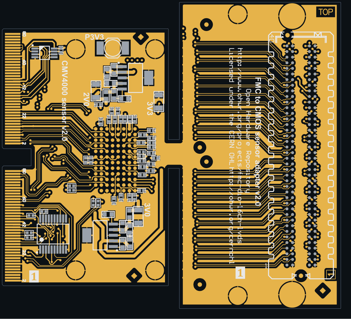
FMC DIO 16CH LVDS A (OHWR0038 R1) is an open-hardware circuit board from the CERN Open Hardware Repository, designed in Altium Designer: a 4-layer board of 76.6 × 69.3 mm with 82 components and 199 nets, published under CERN-OHL-1.1.
review 91% walked · 10 findings: 1 blocker · 4 major · 5 minor (24 items)
Open in the interactive viewerRead the full review
Design review
Probe recorded 10 findings: 1 blocker · 4 major · 5 minor (24 items) on this design. Each is shown here with its reasoning; the full review links every one to the pins, nets and datasheet pages it rests on.
- NetCopperSplitblockerOpen
NetCopperSplit: 6 boards×6
e.g. “P12VF's copper is in 5 pieces: J1.c35 and 3 other piece(s) are not connected to the rest of the net” · 6 different statements
At split:P12VF, split:P3V3F, split:VADJF, split:VDD20, split:VDD33, split:VDDPIX
Each finding, with its own headline
split:P12VFP12VF's copper is in 5 pieces: J1.c35 and 3 other piece(s) are not connected to the rest of the net
P12VF's copper is in 5 pieces: J1.c35 and 3 other piece(s) are not connected to the rest of the net. Piece 1: J1.c37, on TOP_LAYER, over (-6.14, -13.97) to (-5, -13.33). Piece 2: J1.c35, on TOP_LAYER, over (-6.14, -16.51) to (-5.03, -15.87). Piece 3: CON4.75, on TOP_LAYER, MIDLAYER1 and BOTTOM_LAYER, 2 drill(s), over (-35.83, -8.4) to (-32.15, -7.59). Piece 4: CON4.79, on TOP_LAYER, MIDLAYER1 and BOTTOM_LAYER, 2 drill(s), over (-35.9, -6.72) to (-32.65, -5.65). Piece 5: CON4.77, on TOP_LAYER, MIDLAYER1 and BOTTOM_LAYER, 2 drill(s), over (-35.9, -7.4) to (-32.65, -6.9). The export files every one of these pins under the net, so every connectivity check passes; the copper the fab builds leaves them apart. Usually a pour island that touches only one via of its own net, or a track ending short of its copper: join the piece to the net and export again.
split:P3V3FP3V3F's copper is in 7 pieces: J1.d36 and 5 other piece(s) are not connected to the rest of the net
P3V3F's copper is in 7 pieces: J1.d36 and 5 other piece(s) are not connected to the rest of the net. Piece 1: J1.c39, on TOP_LAYER, MIDLAYER1 and BOTTOM_LAYER, 2 drill(s), over (-6.65, -11.43) to (-4.85, -10.26). Piece 2: J1.d36, on TOP_LAYER, MIDLAYER1 and BOTTOM_LAYER, 2 drill(s), over (-7.97, -15.24) to (-6.4, -14.12). Piece 3: J1.d38, on TOP_LAYER, MIDLAYER1 and BOTTOM_LAYER, 2 drill(s), over (-8.07, -12.7) to (-6.43, -11.65). Piece 4: J1.d40, on TOP_LAYER, MIDLAYER1 and BOTTOM_LAYER, 2 drill(s), over (-8.25, -10.16) to (-6.77, -8.89). Piece 5: CON4.80, on BOTTOM_LAYER, over (-27.45, -6.72) to (-25.65, -6.32). Piece 6: CON4.78, on BOTTOM_LAYER, over (-27.45, -7.35) to (-25.65, -6.95). Piece 7: CON4.76, on BOTTOM_LAYER, over (-27.45, -7.99) to (-25.65, -7.59). The export files every one of these pins under the net, so every connectivity check passes; the copper the fab builds leaves them apart. Usually a pour island that touches only one via of its own net, or a track ending short of its copper: join the piece to the net and export again.
split:VADJFVADJF's copper is in 5 pieces: J1.h40 and 3 other piece(s) are not connected to the rest of the net
VADJF's copper is in 5 pieces: J1.h40 and 3 other piece(s) are not connected to the rest of the net. Piece 1: J1.g39, on TOP_LAYER, MIDLAYER1 and BOTTOM_LAYER, 2 drill(s), over (-11.81, -11.43) to (-9.91, -10.31). Piece 2: J1.h40, on TOP_LAYER, MIDLAYER1 and BOTTOM_LAYER, 2 drill(s), over (-13.05, -10.16) to (-11.48, -9.01). Piece 3: CON4.72, on BOTTOM_LAYER, over (-27.45, -9.26) to (-25.65, -8.86). Piece 4: CON4.70, on BOTTOM_LAYER, over (-27.45, -9.89) to (-25.65, -9.49). Piece 5: CON4.68, on BOTTOM_LAYER, over (-27.45, -10.53) to (-25.65, -10.13). The export files every one of these pins under the net, so every connectivity check passes; the copper the fab builds leaves them apart. Usually a pour island that touches only one via of its own net, or a track ending short of its copper: join the piece to the net and export again.
split:VDD20VDD20's copper is in 3 pieces: C7.1 and FB1.2 and 1 other piece(s) are not connected to the rest of the net
VDD20's copper is in 3 pieces: C7.1 and FB1.2 and 1 other piece(s) are not connected to the rest of the net. Piece 1: C1.2, C2.2, C3.2, C4.2, IC1.A7, IC1.C7, IC1.E4, IC1.E7 and 1 more pin(s), on TOP_LAYER, MIDLAYER1 and BOTTOM_LAYER, 7 drill(s), 26.59 mm2 of pour, over (-58.05, -44.68) to (-48.08, -27.11). Piece 2: C7.1 and FB1.2, on TOP_LAYER, MIDLAYER1 and BOTTOM_LAYER, 3 drill(s), over (-56.3, -23.25) to (-52.62, -19.99). Piece 3: C8.2, on TOP_LAYER, MIDLAYER1 and BOTTOM_LAYER, 1 drill(s), over (-54.69, -24.12) to (-54.07, -22.81). The export files every one of these pins under the net, so every connectivity check passes; the copper the fab builds leaves them apart. Usually a pour island that touches only one via of its own net, or a track ending short of its copper: join the piece to the net and export again.
split:VDD33VDD33's copper is in 7 pieces: C35.2, C40.1, IC2.2, IC5.20 and R9.1 and 5 other piece(s) are not connected to the rest of the net
VDD33's copper is in 7 pieces: C35.2, C40.1, IC2.2, IC5.20 and R9.1 and 5 other piece(s) are not connected to the rest of the net. Piece 1: C10.2, C13.2, C14.2, C18.2, C19.2, C32.2, IC1.E2, IC1.F7 and 2 more pin(s), on TOP_LAYER, MIDLAYER1 and BOTTOM_LAYER, 7 drill(s), 8.39 mm2 of pour, over (-50.78, -43.92) to (-42.01, -24.99). Piece 2: C35.2, C40.1, IC2.2, IC5.20 and R9.1, on TOP_LAYER, MIDLAYER1 and BOTTOM_LAYER, 6 drill(s), over (-68.25, -57.7) to (-40.2, -37.49). Piece 3: C37.2, IC3.2 and R12.1, on TOP_LAYER, MIDLAYER1 and BOTTOM_LAYER, 2 drill(s), over (-53.42, -16.51) to (-46.45, -14.66). Piece 4: C17.1, on TOP_LAYER, MIDLAYER1 and BOTTOM_LAYER, 2 drill(s), over (-42.08, -25.12) to (-40.28, -22.62). Piece 5: C24.2, on TOP_LAYER, MIDLAYER1 and BOTTOM_LAYER, 1 drill(s), over (-42.85, -38.38) to (-41.67, -37.76). Piece 6: C30.2, on TOP_LAYER, MIDLAYER1 and BOTTOM_LAYER, 1 drill(s), over (-44.78, -39.31) to (-43.5, -38.67). Piece 7: L1.2, on TOP_LAYER, over (-49.55, -11.82) to (-47.95, -8.82). The export files every one of these pins under the net, so every connectivity check passes; the copper the fab builds leaves them apart. Usually a pour island that touches only one via of its own net, or a track ending short of its copper: join the piece to the net and export again.
split:VDDPIXVDDPIX's copper is in 3 pieces: C26.1 and FB2.2 and 1 other piece(s) are not connected to the rest of the net
VDDPIX's copper is in 3 pieces: C26.1 and FB2.2 and 1 other piece(s) are not connected to the rest of the net. Piece 1: C28.2, C29.2, IC1.E6, IC1.G1 and IC1.G12, on TOP_LAYER, MIDLAYER1 and BOTTOM_LAYER, 3 drill(s), 17.41 mm2 of pour, over (-51.58, -43.95) to (-47.42, -26.58). Piece 2: C26.1 and FB2.2, on TOP_LAYER, MIDLAYER1 and BOTTOM_LAYER, 2 drill(s), over (-48.33, -47.49) to (-44.93, -44.52). Piece 3: C27.2, on TOP_LAYER, MIDLAYER1 and BOTTOM_LAYER, 1 drill(s), over (-46.98, -43.93) to (-45.68, -43.3). The export files every one of these pins under the net, so every connectivity check passes; the copper the fab builds leaves them apart. Usually a pour island that touches only one via of its own net, or a track ending short of its copper: join the piece to the net and export again.
CMV4000 VDD20 set to 2.00 V, below the 2.05 V minimum the current datasheet gives for the fitted Version 2 sensor (IC3 divider R13/R14)
VDD20 of the fitted CMV4000 (Version 2) is set about 50 mV below its specified minimum. IC3's divider R13 6k2 / R14 1k6 gives 2.00 V; the datasheet on file requires 2.05-2.15 V for this sensor version.
The numbers
Quantity Value Source IC3 MCP1826 VADJ 0.410 V nominal (0.402-0.418 V) MCP1826 datasheet p.16 / p.7 P2V0 = VADJ x (1 + R13/R14) 0.410 x 4.875 = 2.00 V (1.93-2.07 V with VADJ and 1% resistor tolerance) computed VDD20 at the sensor P2V0 through ferrite bead FB1, slightly lower at 380 mA readout board CMV4000 VDD20, Version2 min 2.05 / typ 2.1 / max 2.15 V CMV4000 datasheet p.14 CMV4000 VDD20, Version3 2.0 / 2.0 / 2.15 V CMV4000 datasheet p.14 Why Version 2
The fitted part is CMV4000-2E5C1PP. The ordering-code breakdown on datasheet p.6 makes the digit after 'CMV4000-' the Version (sales revision), so this is a Version 2 sensor.
Where the 2.0 V came from
The designer's supply table on schematic sheet 2 quotes 'VDD20 2.0V 1.6V--2.1V', which looks like an earlier datasheet revision's range. The current datasheet (DS000728 v8-01, 2025) no longer supports it for Version 2.
VDD20 feeds sensor pins A7, C7, E4, E7, E8 on OHWR0038 R1 FMC DIO 16CH LVDS A.
- ReferencePlaneDiscontinuitymajorOpen
ReferencePlaneDiscontinuity: 9 boards×9
Checked by the review, stands · Claude walker W3 (Cern session) — Checked: the reference break is read from the copper as stated. Whether it matters depends on the signal's edge rate and the receiver's margin, which no datasheet or app note on file fixes for this net; the impedance step and reflection figures are Probe's model, and the thresholds are its starting values. Layout practice, not a datasheet requirement. Left for the owner.
At along@MIDLAYER1:GND|VDD33, merged:-57,-38.32|-51.16,-43.48, split@MIDLAYER1:GND|VDD33, split@MIDLAYER1:GND|VDDPIX, split@MIDLAYER1:VDD33|VDDPIX, void:GND@MIDLAYER1:hole -69.32,-46.31|-42.3,-18.48 and 3 more
Each finding, with its own headline
along@MIDLAYER1:GND|VDD332 nets run ALONG the split between the GND and VDD33 planes on MIDLAYER1 at 2 places, the longest 1 mm; the impedance rises from 42 ohm to 63 ohm there at worst, 19.5 % of each edge reflected (fastest: NetC16_1 at 100 ps 10-90 %, ASSUMED)
On MIDLAYER1 the GND and VDD33 planes part, and 2 nets run down the slot between them at 2 place(s), rather than across it. This is not a crossing: the return still follows the track, in the plane on its other side and in the slot's edges, so it does not detour. What changes is the track's own impedance. With the plane gone from under it on this side for that length, its field reaches further, to the slot's edges and to the next plane beyond, so its capacitance falls and its impedance rises; every edge travelling down it is partly reflected where it enters the stretch and again where it leaves, by (Z2 - Z1)/(Z2 + Z1). The longer the stretch against the edge's rise, the more of the edge sees the full step. A crossing is generally the worse fault; a mismatch is not free. Over solid plane each track is 42 ohm to 54 ohm; along the slot 63 ohm to 72 ohm, reflecting up to 19.5 % of each edge (a method-of-moments field solve of the cross-section, one dielectric; were the slot's edges to carry none of the return, up to 116 ohm). No place stays within 10 %, the tolerance controlled impedance is commonly built to (the stackup states none), so the finding is a warning. One decision covers the split line's slot: whether these tracks may run down it, or should be moved over solid plane.
- 'NetC16_1' on TOP_LAYER at (-45.94, -35.2), 1.52 mm, running ALONG the split for 0.66 mm, not across it, 42 ohm over solid plane, 63 ohm along it: 19.5 % of each edge reflected; other side: none: the signal layer is outermost
- 'NetC33_1' on TOP_LAYER at (-44.8, -28.97), 1.73 mm, running ALONG the split for 1 mm, not across it, 54 ohm over solid plane, 72 ohm along it: 14.3 % of each edge reflected; other side: none: the signal layer is outermost
Every site is a row of this finding's evidence, keyed by net, layers and position. GET /api/odb/boards/39/reference-planes?group=along%40MIDLAYER1%3AGND%7CVDD33 serves each with its own layer_image region; all of them lie in x -47.77..-43.04, y -36.57..-27.97 mm (board frame, Y up).
Read from the copper as drawn on the reference layer, along each track's centreline at exact breakpoints. The reference is the copper beside the track, never the layer's type or name. Whether it matters depends on each signal's edge rate, which nothing on file states for these nets: a slow static line crosses a split harmlessly, a fast edge does not.
merged:-57,-38.32|-51.16,-43.483 nets cross the slot of 28 drills from (-57, -38.32) to (-51.16, -43.48), whose anti-pads run together in the GND plane on MIDLAYER1, between 3 pairs of drills (fastest: NetC5_1 at 100 ps 10-90 %, ASSUMED)
The GND plane on MIDLAYER1 is cleared round a field of 28 drills from (-57, -38.32) to (-51.16, -43.48), and the clearances run together: the straight line from one drill to the next is bare all the way. 3 nets cross between drills of it at 3 place(s), each listed below with its two drills. Past one drill's anti-pad the return flows round on either side; here it cannot pass between the drills and detours round the whole merged clearance - the slot a row of pins or vias cuts in a plane. One decision covers the slot: whether these tracks may cross it, or the clearances should leave copper between the drills. No crossing has a plane on the track's other side, so the whole return meets the break.
- 'NetC5_1' on TOP_LAYER at (-52.27, -28.67), 1.63 mm between the drills at (-51.65, -28.59) and (-52.92, -29.86) in MIDLAYER1; other side: none: the signal layer is outermost
- 'OUT16_P' on TOP_LAYER at (-54.75, -29.23), 2.9 mm between the drills at (-54.19, -28.59) and (-55.46, -29.86) in MIDLAYER1; other side: none: the signal layer is outermost
- 'OUT1_N' on TOP_LAYER at (-54.78, -40.66), 2.97 mm between the drills at (-55.46, -40.02) and (-55.46, -41.29) in MIDLAYER1; other side: none: the signal layer is outermost
Every site is a row of this finding's evidence, keyed by net, layers and position. GET /api/odb/boards/39/reference-planes?group=merged%3A-57%2C-38.32%7C-51.16%2C-43.48 serves each with its own layer_image region; all of them lie in x -57.03..-50.65, y -42.29..-27.1 mm (board frame, Y up).
Read from the copper as drawn on the reference layer, along each track's centreline at exact breakpoints. The reference is the copper beside the track, never the layer's type or name. Whether it matters depends on each signal's edge rate, which nothing on file states for these nets: a slow static line crosses a split harmlessly, a fast edge does not.
split@MIDLAYER1:GND|VDD335 nets cross the split between the GND and VDD33 planes on MIDLAYER1 at 5 places, with no plane on the track's other side (fastest: NetC22_1 at 100 ps 10-90 %, ASSUMED)
On MIDLAYER1 the GND and VDD33 planes part, and 5 nets cross from one to the other at 5 place(s). The return current cannot follow a track across; it detours to wherever the two planes are joined (a stitching capacitor, or the source), and the loop it opens radiates and couples. One decision covers the boundary: whether it is stitched near these crossings, or the nets crossing it are slow enough not to care. Tracks that run ALONG this split, down the slot rather than across it, are a finding of their own: theirs is an impedance step, not a detour. At 0 of the 5 crossing(s) the track's other neighbour carries a plane, which the return can use there; 5 are on an outer layer, with no other neighbour. No crossing has a plane on the track's other side, so the whole return meets the break.
- 'NetC22_1' on TOP_LAYER at (-46.16, -32.88), 0.82 mm; other side: none: the signal layer is outermost
- 'NetC23_1' on TOP_LAYER at (-46.26, -31.77), 0.53 mm; other side: none: the signal layer is outermost
- 'NetC31_1' on TOP_LAYER at (-46.9, -27.11), 0.58 mm; other side: none: the signal layer is outermost
- 'NetC32_1' on TOP_LAYER at (-46.26, -30.5), 0.53 mm; other side: none: the signal layer is outermost
- 'NetIC1_G8' on TOP_LAYER at (-46.33, -34.3), 0.53 mm; other side: none: the signal layer is outermost
Every site is a row of this finding's evidence, keyed by net, layers and position. GET /api/odb/boards/39/reference-planes?group=split%40MIDLAYER1%3AGND%7CVDD33 serves each with its own layer_image region; all of them lie in x -48.1..-44.84, y -35.3..-25.9 mm (board frame, Y up).
Read from the copper as drawn on the reference layer, along each track's centreline at exact breakpoints. The reference is the copper beside the track, never the layer's type or name. Whether it matters depends on each signal's edge rate, which nothing on file states for these nets: a slow static line crosses a split harmlessly, a fast edge does not.
split@MIDLAYER1:GND|VDDPIX5 nets cross the split between the GND and VDDPIX planes on MIDLAYER1 at 5 places, with no plane on the track's other side (fastest: NetC10_1 at 100 ps 10-90 %, ASSUMED)
On MIDLAYER1 the GND and VDDPIX planes part, and 5 nets cross from one to the other at 5 place(s). The return current cannot follow a track across; it detours to wherever the two planes are joined (a stitching capacitor, or the source), and the loop it opens radiates and couples. One decision covers the boundary: whether it is stitched near these crossings, or the nets crossing it are slow enough not to care. Tracks that run ALONG this split, down the slot rather than across it, are a finding of their own: theirs is an impedance step, not a detour. At 0 of the 5 crossing(s) the track's other neighbour carries a plane, which the return can use there; 5 are on an outer layer, with no other neighbour. No crossing has a plane on the track's other side, so the whole return meets the break.
- 'NetC10_1' on TOP_LAYER at (-48.48, -28.46), 0.69 mm; other side: none: the signal layer is outermost
- 'NetC11_1' on TOP_LAYER at (-49.75, -28.36), 0.53 mm; other side: none: the signal layer is outermost
- 'NetC15_1' on TOP_LAYER at (-46.52, -36.84), 1.45 mm; other side: none: the signal layer is outermost
- 'NetC30_1' on TOP_LAYER at (-46.66, -38.12), 1.85 mm; other side: none: the signal layer is outermost
- 'NetC9_1' on TOP_LAYER at (-51, -28.29), 0.53 mm; other side: none: the signal layer is outermost
Every site is a row of this finding's evidence, keyed by net, layers and position. GET /api/odb/boards/39/reference-planes?group=split%40MIDLAYER1%3AGND%7CVDDPIX serves each with its own layer_image region; all of them lie in x -52..-44.78, y -39.57..-27.02 mm (board frame, Y up).
Read from the copper as drawn on the reference layer, along each track's centreline at exact breakpoints. The reference is the copper beside the track, never the layer's type or name. Whether it matters depends on each signal's edge rate, which nothing on file states for these nets: a slow static line crosses a split harmlessly, a fast edge does not.
split@MIDLAYER1:VDD33|VDDPIX'NetC10_1' crosses the split between the VDD33 and VDDPIX planes on MIDLAYER1 at 1 place, with no plane on the track's other side (fastest: NetC10_1 at 100 ps 10-90 %, ASSUMED)
On MIDLAYER1 the VDD33 and VDDPIX planes part, and 'NetC10_1' crosses from one to the other at 1 place(s). The return current cannot follow a track across; it detours to wherever the two planes are joined (a stitching capacitor, or the source), and the loop it opens radiates and couples. One decision covers the boundary: whether it is stitched near these crossings, or the nets crossing it are slow enough not to care. Tracks that run ALONG this split, down the slot rather than across it, are a finding of their own: theirs is an impedance step, not a detour. At 0 of the 1 crossing(s) the track's other neighbour carries a plane, which the return can use there; 1 are on an outer layer, with no other neighbour. No crossing has a plane on the track's other side, so the whole return meets the break.
- 'NetC10_1' on TOP_LAYER at (-48.48, -29.99), 0.25 mm; other side: none: the signal layer is outermost
Every site is a row of this finding's evidence, keyed by net, layers and position. GET /api/odb/boards/39/reference-planes?group=split%40MIDLAYER1%3AVDD33%7CVDDPIX serves each with its own layer_image region; all of them lie in x -49.48..-47.48, y -31.12..-28.87 mm (board frame, Y up).
Read from the copper as drawn on the reference layer, along each track's centreline at exact breakpoints. The reference is the copper beside the track, never the layer's type or name. Whether it matters depends on each signal's edge rate, which nothing on file states for these nets: a slow static line crosses a split harmlessly, a fast edge does not.
void:GND@MIDLAYER1:hole -69.32,-46.31|-42.3,-18.4823 nets cross one void in the GND plane on MIDLAYER1 and the GND plane on TOP_LAYER at 13 places, the longest 12.83 mm; 43 over tracks of other nets routed inside it (fastest: NetIC1_G2 at 100 ps 10-90 %, ASSUMED)
Along 'OUT9_N' on MIDLAYER1, the GND plane on TOP_LAYER has 12.83 mm under the track with copper of OUT10_P, OUT11_N, OUT11_P, OUT13_N, OUT13_P, not a plane, at (-54.13, -34.3), running to the end of the track. No single drill's anti-pad and no landing explains it: a clearance is excused only when it holds a drill and is drawn round it, or the track ends in it on the net's own pad or via, or runs through its own via's clearance and no farther. The return current detours round the void. 43 of the crossings pass over tracks of other nets routed inside the hole on the reference layer: the plane is absent there, and those tracks stand in it. 21 of them run ALONG the bare copper, parallel to its edges, rather than across it (the longest 6.28 mm). 13 places on 23 net(s) cross it, listed below, the longest first. What cleared it: the hole at x -69.32..-42.3, y -46.31..-18.48. One decision covers the void: whether these tracks may cross it, or the plane should be filled under them. 0 of the 43 crossing(s) have a plane on the track's other side at most twice as far away as the broken one (to first order each plane beside a stripline carries a share of the return inversely proportional to its distance from the track). The rest leave most or all of the return to the break, so the finding is a warning.
- one crossing of two tracks, seen from each: 'OUT10_N' on TOP_LAYER at (-59.18, -33.03), 5.12 mm, running ALONG the bare copper for 2.89 mm, not across it over copper of OUT8_N, OUT8_P, not a plane, to the end of the track; other side: none: the signal layer is outermost / 'OUT10_P' on TOP_LAYER at (-58.71, -32.94), 5.17 mm, running ALONG the bare copper for 1.99 mm, not across it over copper of OUT8_N, OUT8_P, OUT9_N, not a plane, to the end of the track; other side: none: the signal layer is outermost / 'OUT11_N' on TOP_LAYER at (-54.88, -33.04), 5 mm, running ALONG the bare copper for 3.39 mm, not across it over copper of OUT9_P, not a plane, to the end of the track; other side: none: the signal layer is outermost / 'OUT11_N' on TOP_LAYER at (-59.8, -30.57), 3.56 mm over copper of OUT8_N, OUT8_P, OUT9_N, OUT9_P, not a plane; other side: none: the signal layer is outermost / 'OUT11_P' on TOP_LAYER at (-59.8, -30.02), 3.56 mm over copper of OUT8_N, OUT8_P, OUT9_N, OUT9_P, not a plane; other side: none: the signal layer is outermost / 'OUT13_N' on TOP_LAYER at (-61.01, -27.79), 4.82 mm, running ALONG the bare copper for 1.18 mm, not across it over copper of OUT8_N, OUT8_P, OUT9_N, OUT9_P, not a plane; other side: none: the signal layer is outermost / 'OUT13_P' on TOP_LAYER at (-60.73, -27.51), 5.14 mm, running ALONG the bare copper for 1.5 mm, not across it over copper of OUT8_P, OUT9_N, OUT9_P, OUT8_N, not a plane; other side: none: the signal layer is outermost / 'OUT8_N' on MIDLAYER1 at (-61.01, -27.78), 6.56 mm, running ALONG the bare copper for 1.2 mm, not across it over copper of OUT10_N, OUT10_P, OUT11_N, OUT11_P, OUT13_N, OUT13_P, not a plane; other side: GND on PLANE_L3GND, 1 mm from the track against 0.11 mm to TOP_LAYER: 90% of the return on TOP_LAYER / 'OUT8_P' on MIDLAYER1 at (-60.72, -27.5), 6.89 mm, running ALONG the bare copper for 1.53 mm, not across it over copper of OUT10_N, OUT10_P, OUT11_N, OUT11_P, OUT13_N, OUT13_P, not a plane; other side: GND on PLANE_L3GND, 1 mm from the track against 0.11 mm to TOP_LAYER: 90% of the return on TOP_LAYER / 'OUT9_N' on MIDLAYER1 at (-54.13, -34.3), 12.83 mm, running ALONG the bare copper for 3.22 mm, not across it over copper of OUT10_P, OUT11_N, OUT11_P, OUT13_N, OUT13_P, not a plane, to the end of the track; other side: GND on PLANE_L3GND, 1 mm from the track against 0.11 mm to TOP_LAYER: 90% of the return on TOP_LAYER / 'OUT9_P' on MIDLAYER1 at (-54.78, -33.04), 11.7 mm, running ALONG the bare copper for 4.66 mm, not across it over copper of OUT11_N, OUT11_P, OUT13_N, OUT13_P, not a plane, to the end of the track; other side: GND on PLANE_L3GND, 1 mm from the track against 0.11 mm to TOP_LAYER: 90% of the return on TOP_LAYER
- 'OUT6_N' on TOP_LAYER at (-54.65, -38.11), 8.63 mm, running ALONG the bare copper for 5.92 mm, not across it over copper of OUT3_P, OUT3_N, not a plane, to the end of the track; other side: none: the signal layer is outermost
- one crossing of two tracks, seen from each: 'OUT6_P' on TOP_LAYER at (-54.78, -36.85), 7.64 mm, running ALONG the bare copper for 6.28 mm, not across it over copper of OUT8_N, OUT3_P, not a plane, to the end of the track; other side: none: the signal layer is outermost / 'OUT8_N' on MIDLAYER1 at (-54.7, -36.85), 7.13 mm, running ALONG the bare copper for 3.7 mm, not across it over copper of OUT6_P, GND, not a plane, to the end of the track; other side: GND on PLANE_L3GND, 1 mm from the track against 0.11 mm to TOP_LAYER: 90% of the return on TOP_LAYER
- one crossing of two tracks, seen from each: 'OUT11_P' on TOP_LAYER at (-54.68, -31.77), 4.71 mm, running ALONG the bare copper for 2.75 mm, not across it over copper of OUT14_N, not a plane, to the end of the track; other side: none: the signal layer is outermost / 'OUT13_P' on TOP_LAYER at (-57.53, -30.71), 1.91 mm over copper of OUT14_N, not a plane, to the end of the track; other side: none: the signal layer is outermost / 'OUT14_N' on MIDLAYER1 at (-54.64, -31.77), 7.53 mm, running ALONG the bare copper for 3.68 mm, not across it over copper of OUT11_P, OUT13_P, not a plane, to the end of the track; other side: GND on PLANE_L3GND, 1 mm from the track against 0.11 mm to TOP_LAYER: 90% of the return on TOP_LAYER
- one crossing of two tracks, seen from each: 'OUT16_N' on TOP_LAYER at (-60.03, -26.28), 6.61 mm, running ALONG the bare copper for 2.44 mm, not across it over copper of OUT9_P, OUT8_N, OUT8_P, OUT9_N, not a plane; other side: none: the signal layer is outermost / 'OUT16_P' on TOP_LAYER at (-59.66, -26.05), 6.92 mm, running ALONG the bare copper for 2.65 mm, not across it over copper of OUT8_N, OUT8_P, OUT9_N, OUT9_P, not a plane; other side: none: the signal layer is outermost / 'OUT8_P' on MIDLAYER1 at (-63.56, -24.66), 1.89 mm over copper of OUT16_P, OUT16_N, not a plane; other side: GND on PLANE_L3GND, 1 mm from the track against 0.11 mm to TOP_LAYER: 90% of the return on TOP_LAYER / 'OUT9_N' on MIDLAYER1 at (-60.3, -26.27), 4.22 mm, running ALONG the bare copper for 2.36 mm, not across it over copper of OUT16_P, OUT16_N, not a plane; other side: GND on PLANE_L3GND, 1 mm from the track against 0.11 mm to TOP_LAYER: 90% of the return on TOP_LAYER / 'OUT9_P' on MIDLAYER1 at (-60.01, -25.99), 4.56 mm, running ALONG the bare copper for 2.68 mm, not across it over copper of OUT16_N, OUT16_P, not a plane; other side: GND on PLANE_L3GND, 1 mm from the track against 0.11 mm to TOP_LAYER: 90% of the return on TOP_LAYER
- one crossing of two tracks, seen from each: 'OUT14_N' on MIDLAYER1 at (-57.84, -27.49), 1.93 mm over copper of OUT16_N, OUT16_P, not a plane; other side: GND on PLANE_L3GND, 1 mm from the track against 0.11 mm to TOP_LAYER: 90% of the return on TOP_LAYER / 'OUT14_P' on MIDLAYER1 at (-54.59, -30.49), 5.54 mm, running ALONG the bare copper for 2.82 mm, not across it over copper of OUT16_N, not a plane, to the end of the track; other side: GND on PLANE_L3GND, 1 mm from the track against 0.11 mm to TOP_LAYER: 90% of the return on TOP_LAYER / 'OUT14_P' on MIDLAYER1 at (-57.44, -27.9), 1.93 mm over copper of OUT16_N, OUT16_P, not a plane; other side: GND on PLANE_L3GND, 1 mm from the track against 0.11 mm to TOP_LAYER: 90% of the return on TOP_LAYER / 'OUT16_N' on TOP_LAYER at (-54.66, -30.49), 4.11 mm, running ALONG the bare copper for 2.96 mm, not across it over copper of OUT14_P, not a plane, to the end of the track; other side: none: the signal layer is outermost / 'OUT16_N' on TOP_LAYER at (-57.17, -29.14), 1.91 mm over copper of OUT14_N, OUT14_P, not a plane; other side: none: the signal layer is outermost / 'OUT16_P' on TOP_LAYER at (-57.17, -28.54), 1.91 mm over copper of OUT14_N, OUT14_P, not a plane; other side: none: the signal layer is outermost
- one crossing of two tracks, seen from each: 'OUT8_N' on MIDLAYER1 at (-64.95, -23.84), 1.66 mm over copper of OUTCLK_P, OUTCLK_N, not a plane; other side: GND on PLANE_L3GND, 1 mm from the track against 0.11 mm to TOP_LAYER: 90% of the return on TOP_LAYER / 'OUT8_P' on MIDLAYER1 at (-64.38, -23.84), 1.87 mm over copper of OUTCLK_P, OUTCLK_N, not a plane; other side: GND on PLANE_L3GND, 1 mm from the track against 0.11 mm to TOP_LAYER: 90% of the return on TOP_LAYER / 'OUT9_N' on MIDLAYER1 at (-63.67, -22.91), 1.89 mm over copper of OUTCLK_P, OUTCLK_N, not a plane; other side: GND on PLANE_L3GND, 1 mm from the track against 0.11 mm to TOP_LAYER: 90% of the return on TOP_LAYER / 'OUT9_P' on MIDLAYER1 at (-63.09, -22.91), 1.89 mm over copper of OUTCLK_P, OUTCLK_N, not a plane; other side: GND on PLANE_L3GND, 1 mm from the track against 0.11 mm to TOP_LAYER: 90% of the return on TOP_LAYER / 'OUTCLK_N' on TOP_LAYER at (-63.82, -23.57), 3.85 mm over copper of OUT8_N, OUT8_P, OUT9_N, OUT9_P, not a plane, to the end of the track; other side: none: the signal layer is outermost / 'OUTCLK_P' on TOP_LAYER at (-64.22, -23.18), 4.23 mm over copper of OUT8_P, OUT9_N, OUT9_P, OUT8_N, not a plane, to the end of the track; other side: none: the signal layer is outermost
- 'OUT1_P' on TOP_LAYER at (-54.73, -39.39), 3.78 mm, running ALONG the bare copper for 2.53 mm, not across it over copper of OUT3_N, not a plane, to the end of the track; other side: none: the signal layer is outermost
- 'OUT4_N' on TOP_LAYER at (-61.44, -36.49), 3.1 mm over copper of OUT3_P, OUT3_N, not a plane; other side: none: the signal layer is outermost
- one crossing of two tracks, seen from each: 'OUT14_N' on MIDLAYER1 at (-61.45, -22.91), 1.89 mm over copper of OUTCLK_P, OUTCLK_N, not a plane; other side: GND on PLANE_L3GND, 1 mm from the track against 0.11 mm to TOP_LAYER: 90% of the return on TOP_LAYER / 'OUT14_P' on MIDLAYER1 at (-60.88, -22.91), 1.89 mm over copper of OUTCLK_P, OUTCLK_N, not a plane; other side: GND on PLANE_L3GND, 1 mm from the track against 0.11 mm to TOP_LAYER: 90% of the return on TOP_LAYER / 'OUTCLK_N' on TOP_LAYER at (-59.84, -23.57), 1.91 mm over copper of OUT14_N, OUT14_P, not a plane; other side: none: the signal layer is outermost / 'OUTCLK_P' on TOP_LAYER at (-60.23, -23.18), 1.91 mm over copper of OUT14_N, OUT14_P, not a plane; other side: none: the signal layer is outermost
- 'OUT4_P' on TOP_LAYER at (-60.89, -36.49), 1.82 mm over copper of OUT3_P, OUT3_N, not a plane; other side: none: the signal layer is outermost
- 'T_EXP2_3V3' on TOP_LAYER at (-46.54, -40.65), 1.7 mm over copper of VDD33, not a plane, to the end of the track; other side: none: the signal layer is outermost
- and 1 more
Every site is a row of this finding's evidence, keyed by net, layers and position. GET /api/odb/boards/39/reference-planes?group=void%3AGND%40MIDLAYER1%3Ahole%20-69.32%2C-46.31%7C-42.3%2C-18.48 serves each with its own layer_image region; all of them lie in x -67.24..-45, y -42.92..-21.7 mm (board frame, Y up).
Read from the copper as drawn on the reference layer, along each track's centreline at exact breakpoints. The reference is the copper beside the track, never the layer's type or name. Whether it matters depends on each signal's edge rate, which nothing on file states for these nets: a slow static line crosses a split harmlessly, a fast edge does not.
void:GND@MIDLAYER1:hole -70.76,-54.93|-62.15,-48.035 nets cross one void in the GND plane on MIDLAYER1 at 5 places, the longest 5.04 mm; 5 over tracks of other nets routed inside it (fastest: NetIC1_F4 at 100 ps 10-90 %, ASSUMED)
Along 'NetIC1_F4' on TOP_LAYER, the GND plane on MIDLAYER1 has 5.04 mm under the track with copper of SPI_EN, not a plane, at (-68.12, -50.26), running to the end of the track. No single drill's anti-pad and no landing explains it: a clearance is excused only when it holds a drill and is drawn round it, or the track ends in it on the net's own pad or via, or runs through its own via's clearance and no farther. The return current detours round the void. 5 of the crossings pass over tracks of other nets routed inside the hole on the reference layer: the plane is absent there, and those tracks stand in it. 4 of them run ALONG the bare copper, parallel to its edges, rather than across it (the longest 1.6 mm). 5 places on 5 net(s) cross it, listed below, the longest first. What cleared it: the hole at x -70.76..-62.15, y -54.93..-48.03. One decision covers the void: whether these tracks may cross it, or the plane should be filled under them. No crossing has a plane on the track's other side, so the whole return meets the break.
- 'NetIC1_F4' on TOP_LAYER at (-68.12, -50.26), 5.04 mm, running ALONG the bare copper for 1.6 mm, not across it over copper of SPI_EN, not a plane, to the end of the track; other side: none: the signal layer is outermost
- 'SYS_RES_N' on TOP_LAYER at (-66.29, -52.38), 4.3 mm, running ALONG the bare copper for 0.49 mm, not across it over copper of SPI_EN, not a plane; other side: none: the signal layer is outermost
- 'SYS_RES_N_3V3' on TOP_LAYER at (-65.29, -50.44), 3.42 mm, running ALONG the bare copper for 0.71 mm, not across it over copper of SPI_EN, not a plane; other side: none: the signal layer is outermost
- 'T_EXP1' on TOP_LAYER at (-64.78, -50.51), 1.8 mm, running ALONG the bare copper for 0.46 mm, not across it over copper of SPI_EN, not a plane, to the end of the track; other side: none: the signal layer is outermost
- 'SPI_EN' on TOP_LAYER at (-70.23, -48.92), 1.1 mm over copper of SPI_CLK, not a plane, to the end of the track; other side: none: the signal layer is outermost
Every site is a row of this finding's evidence, keyed by net, layers and position. GET /api/odb/boards/39/reference-planes?group=void%3AGND%40MIDLAYER1%3Ahole%20-70.76%2C-54.93%7C-62.15%2C-48.03 serves each with its own layer_image region; all of them lie in x -71.51..-63.78, y -54.89..-47.92 mm (board frame, Y up).
Read from the copper as drawn on the reference layer, along each track's centreline at exact breakpoints. The reference is the copper beside the track, never the layer's type or name. Whether it matters depends on each signal's edge rate, which nothing on file states for these nets: a slow static line crosses a split harmlessly, a fast edge does not.
void:GND@MIDLAYER1:hole -72.3,-23.17|-70.35,-19.552 nets cross one void in the GND plane on MIDLAYER1 at 2 places, the longest 1.08 mm; 2 over tracks of other nets routed inside it (fastest: NetCON2_34 at 100 ps 10-90 %, ASSUMED)
Along 'NetCON2_36' on TOP_LAYER, the GND plane on MIDLAYER1 has 1.08 mm under the track with copper of NetCON2_32, not a plane, at (-71.54, -21.05), the same plane on both sides. No single drill's anti-pad and no landing explains it: a clearance is excused only when it holds a drill and is drawn round it, or the track ends in it on the net's own pad or via, or runs through its own via's clearance and no farther. The return current detours round the void. 2 of the crossings pass over tracks of other nets routed inside the hole on the reference layer: the plane is absent there, and those tracks stand in it. 2 places on 2 net(s) cross it, listed below, the longest first. What cleared it: the hole at x -72.3..-70.35, y -23.17..-19.55. One decision covers the void: whether these tracks may cross it, or the plane should be filled under them. No crossing has a plane on the track's other side, so the whole return meets the break.
- 'NetCON2_36' on TOP_LAYER at (-71.54, -21.05), 1.08 mm over copper of NetCON2_32, not a plane; other side: none: the signal layer is outermost
- 'NetCON2_34' on TOP_LAYER at (-71.53, -21.48), 1.02 mm over copper of NetCON2_32, not a plane; other side: none: the signal layer is outermost
Every site is a row of this finding's evidence, keyed by net, layers and position. GET /api/odb/boards/39/reference-planes?group=void%3AGND%40MIDLAYER1%3Ahole%20-72.3%2C-23.17%7C-70.35%2C-19.55 serves each with its own layer_image region; all of them lie in x -72.75..-69.71, y -22.48..-19.93 mm (board frame, Y up).
Read from the copper as drawn on the reference layer, along each track's centreline at exact breakpoints. The reference is the copper beside the track, never the layer's type or name. Whether it matters depends on each signal's edge rate, which nothing on file states for these nets: a slow static line crosses a split harmlessly, a fast edge does not.
void:routed@MIDLAYER1|TOP_LAYER2 nets on MIDLAYER1 cross the tracks routed through the GND pour on TOP_LAYER at 2 places, the longest 6.84 mm; 1 runs ALONG the cut round another net's track (fastest: OUT8_N at 100 ps 10-90 %, ASSUMED)
The GND pour on TOP_LAYER is cleared round tracks routed through it, and tracks on MIDLAYER1, which take that pour as their reference, cross them: for the width of each cut the return has no plane under it and detours round the cut. 2 place(s) on 2 net(s). 1 of the crossings run ALONG the cut round another net's track rather than across it, parallel to its edges (the longest 4.07 mm): over or right beside that track, broadside to it as well as off the plane. One decision covers the layer pair: whether these layers may take a pour their own tracks cut as the reference, or the routing or the stackup should give the tracks a plane that is not cut where they cross. 0 of the 2 crossing(s) have a plane on the track's other side at most twice as far away as the broken one (to first order each plane beside a stripline carries a share of the return inversely proportional to its distance from the track). The rest leave most or all of the return to the break, so the finding is a warning.
- 'OUT8_P' on MIDLAYER1 at (-55.84, -35.58), 6.84 mm, running ALONG the bare copper for 4.07 mm, not across it over copper of VDD20, not a plane, to the end of the track; other side: GND on PLANE_L3GND, 1 mm from the track against 0.11 mm to TOP_LAYER: 90% of the return on TOP_LAYER
- 'OUT8_N' on MIDLAYER1 at (-64.13, -24.66), 1.89 mm over copper of OUT16_P, OUT16_N, not a plane; other side: GND on PLANE_L3GND, 1 mm from the track against 0.11 mm to TOP_LAYER: 90% of the return on TOP_LAYER
Every site is a row of this finding's evidence, keyed by net, layers and position. GET /api/odb/boards/39/reference-planes?group=void%3Arouted%40MIDLAYER1%7CTOP_LAYER serves each with its own layer_image region; all of them lie in x -65.34..-50.65, y -37.21..-23.45 mm (board frame, Y up).
Read from the copper as drawn on the reference layer, along each track's centreline at exact breakpoints. The reference is the copper beside the track, never the layer's type or name. Whether it matters depends on each signal's edge rate, which nothing on file states for these nets: a slow static line crosses a split harmlessly, a fast edge does not.
- PartLifecyclemajorOpen
SN74LVC244ADBRG4 on IC5: the distributor catalogue reports "Discontinued at DigiKey" for Texas Instruments's SN74LVC244ADBRG4
SN74LVC244ADBRG4 on IC5: the distributor catalogue reports "Discontinued at DigiKey" for Texas Instruments's SN74LVC244ADBRG4 — a sourcing/longevity risk to confirm against the MANUFACTURER before acting. That is the maker this board's BOM names (TEXAS INSTRUMENTS). A distributor delisting is not the same claim as the part being unavailable; check the vendor's own lifecycle/product-change notice for the status and any named successor. Re-read the source: GET /api/odb/parts/SN74LVC244ADBRG4/providers (which provider said it, the maker and part number it matched, its own words, and when we asked). No approved alternate is recorded for this position.
At IC5
- FiducialMissingmajorOpen
The bottom side carries 8 SMT component(s) and no fiducial was found on it
The bottom side carries 8 SMT component(s) but no fiducial was found on it — a placement machine has no optical reference to align to. Probe found no pad labelled .pad_usage=g_fiducial/l_fiducial (basis pad_usage); no single-pad, netless, undrilled component whose 0.5-3 mm round pad has a concentric solder-mask opening at least 1.5x its diameter with no other copper inside it (basis geometry); and no component whose refdes starts FID or whose part or package name contains FIDUCIAL (basis footprint-name). The other side has 3, found by footprint-name (3). If your library names fiducials something Probe does not recognise, mark this benign — disposition_finding(rule='FiducialMissing', entity='bottom', status='benign', reason=…) — the name match only ever silences this check, it never asserts anything. If the side really has no fiducial, say so with status='confirmed': that answers the finding and keeps it gating release.
At bottom
Sensor control inputs float until the carrier drives them: IC5 SN74LVC244A inputs have no pull resistors, so the CMV4000's SYS_RES_N and SPI_EN are undefined at power-up
What
On OHWR0038 R1 FMC DIO 16CH LVDS A (CMV4000 sensor head), the carrier drives the sensor's control lines through IC5 SN74LVC244A. The lines are CLK_IN, SYS_RES_N, FRAME_REQ, SPI_EN, SPI_CLK, SPI_IN, T_EXP1 and T_EXP2, and their path is card-edge contacts CON1.57/40/54/46/42/52/28/30 -> IC5 A inputs -> IC5 Y outputs -> IC1. IC5 is powered from VDD33, and both OE pins (1, 19) are tied to GND, so it always drives. None of the eight input nets has a pull-up or pull-down on the head. Each input net (e.g. SYS_RES_N = {CON1.40, IC5.4}, SPI_EN = {CON1.46, IC5.8}) has exactly two ends.
Why it matters
- Until the carrier's FPGA is configured and drives these LA pins, the LVC244 inputs float. The TI datasheet (p.12) says not to leave standard CMOS inputs floating during operation, and to consider a pull-up or pull-down if a system does not always drive an input.
- The CMV4000 datasheet (p.26 Table 9) says SYS_RES_N 'must be kept low during start-up'. The head cannot guarantee that; it depends entirely on the carrier's pre-configuration I/O state.
- SPI_EN is active high (p.26: 'When this pin is high the data should be written/read on the SPI'), so a floating or pulled-up carrier pin can leave the SPI selected.
No fiducials on the bottom side, which carries the 0.635 mm pitch MEC6 sockets CON3/CON4 and 0402 resistors R21-R24
No fiducials on the bottom side of OHWR0038 R1 FMC DIO 16CH LVDS A, which is an SMT assembly side carrying the 0.635 mm pitch MEC6 sockets CON3/CON4 and 0402 resistors R21-R24.
What is on the bottom
- CON3 and CON4: Samtec MEC6-140-02-L-DV-A, 0.635 mm pitch surface-mount edge-card sockets, 80 contacts each (MEC6 document, p.1).
- R21-R24 (0402).
- The through-hole CMV4000 IC1.
Where the fiducials are
Fiducial Side Position (mm) FTG1 top (-45.3, -7.8) FTG2 top (-46.8, -61.8) FTG3 top (-4.1, -65.1) These (BOM 'Fiducial Target', footprint FIDUCIAL_TOP_S100-200) are the only fiducial footprints in the design. Neither the bottom-side placement nor the bottom copper/paste/silk render shows a fiducial, and the export has no pad marked as a fiducial on either side.
Schematic title blocks carry no revision, designer or checker, and wrong sheet numbering ('4 of 5', '* of *') for a two-sheet set
The two schematic sheets of OHWR0038 R1 FMC DIO 16CH LVDS A carry no revision, designer or checker, number themselves '4 of 5' and '* of *', and share a project name that describes a different product.
The sheets are rendered from the repository's fmc_connector.SchDoc and FMC_DIO_16_LVDS.SchDoc.
Title blocks
Sheet 2 holds the CMV4000 sensor, LDOs, EEPROM and buffer.
Field Sheet 1 'FMC Connector Fanout' Sheet 2 'FMC_DIO_16_LVDS' Sheet 4 of 5 '*' of '*' Rev '-' '*' Designer / Drawn by / Check.by empty empty Project/Equipment 'FMC_DIO_16ch_LVDS' 'FMC_DIO_16ch_LVDS' Why it matters
- The shared project name describes a 16-channel LVDS digital-I/O card, while the content is a CMV4000 image-sensor head on an FMC adaptor.
- The last-modified and print dates in the blocks (2026-09-22) come from the conversion re-export, not the design.
No reference designators on the top silkscreen: none of the 70-odd top-side parts (IC2-IC5, L1, FB1/FB2, all R and C) is labelled
The top silkscreen of OHWR0038 R1 FMC DIO 16CH LVDS A carries no reference designator for any of its 70-odd top-side parts (IC2-IC5, L1, FB1/FB2, all R and C, J1).
What the top overlay carries
Layer TOP_OVERLAY, rendered at 29 px/mm over the sensor-head area and 17 px/mm over the FMC adaptor:
- component outlines;
- pin-1 dots on IC2-IC5;
- rail labels 'P3V3', '2V0', '3V3', '3V0';
- the card-edge contact numbers;
- the board titles 'CMV4000 sensor v2.0' and 'FMC to CMOS sensor adapter v2.0', with the OHWR/CERN OHL text.
What has no designator
- Top: IC2, IC3, IC4, IC5, L1, FB1, FB2, R1, R8-R20, R25, R26, C1-C40, J1.
- Bottom: IC1 and R21-R24. (CON1, CON3 and CON4 are labelled.)
- ReferencePlaneDiscontinuityminorOpen
ReferencePlaneDiscontinuity: 2 boards×2
Checked by the review, stands · Claude walker W3 (Cern session) — Checked: the reference break is read from the copper as stated. Whether it matters depends on the signal's edge rate and the receiver's margin, which no datasheet or app note on file fixes for this net; the impedance step and reflection figures are Probe's model, and the thresholds are its starting values. Layout practice, not a datasheet requirement. Left for the owner.
At merged:-69.1,-53.17|-62.8,-54.27, merged:-8.69,-20.01|-7.85,-19.19
Each finding, with its own headline
merged:-69.1,-53.17|-62.8,-54.27'SPI_EN' crosses between the drills at (-64.1, -52.17) and (-62.9, -52.87), whose anti-pads run together in the GND plane on MIDLAYER1 (fastest: SPI_EN at 2 ns 10-90 %, suggested by its name)
Along 'SPI_EN' on TOP_LAYER, the GND plane on MIDLAYER1 is cleared round the drills at (-64.1, -52.17) and (-62.9, -52.87), and the two clearances run together: the straight line from one drill to the other is bare all the way, and the track crosses it, over 1.2 mm of bare stretch at (-63.48, -52.58). Past one drill's anti-pad the return flows round on either side; here it cannot pass between the drills and detours round the whole merged clearance - the slot a row of pins or vias cuts in a plane. No crossing has a plane on the track's other side, so the whole return meets the break.
- 'SPI_EN' on TOP_LAYER at (-63.48, -52.58), 1.2 mm between the drills at (-64.1, -52.17) and (-62.9, -52.87) in MIDLAYER1; other side: none: the signal layer is outermost
Every site is a row of this finding's evidence, keyed by net, layers and position. GET /api/odb/boards/39/reference-planes?group=merged%3A-69.1%2C-53.17%7C-62.8%2C-54.27 serves each with its own layer_image region; all of them lie in x -64.48..-62.48, y -54.18..-50.98 mm (board frame, Y up).
Read from the copper as drawn on the reference layer, along each track's centreline at exact breakpoints. The reference is the copper beside the track, never the layer's type or name. Whether it matters depends on each signal's edge rate, which nothing on file states for these nets: a slow static line crosses a split harmlessly, a fast edge does not.
merged:-8.69,-20.01|-7.85,-19.19'P3V3_AUXF' crosses between the drills at (-8.69, -20.01) and (-7.85, -19.19), whose anti-pads run together in the GND plane on MIDLAYER1 (fastest: P3V3_AUXF at 20 ns 10-90 %, suggested by its name)
Along 'P3V3_AUXF' on TOP_LAYER, the GND plane on MIDLAYER1 is cleared round the drills at (-8.69, -20.01) and (-7.85, -19.19), and the two clearances run together: the straight line from one drill to the other is bare all the way, and the track crosses it, over 0.82 mm of bare stretch at (-8.26, -19.6). Past one drill's anti-pad the return flows round on either side; here it cannot pass between the drills and detours round the whole merged clearance - the slot a row of pins or vias cuts in a plane. No crossing has a plane on the track's other side, so the whole return meets the break.
- 'P3V3_AUXF' on TOP_LAYER at (-8.26, -19.6), 0.82 mm between the drills at (-8.69, -20.01) and (-7.85, -19.19) in MIDLAYER1; other side: none: the signal layer is outermost
Every site is a row of this finding's evidence, keyed by net, layers and position. GET /api/odb/boards/39/reference-planes?group=merged%3A-8.69%2C-20.01%7C-7.85%2C-19.19 serves each with its own layer_image region; all of them lie in x -9.55..-6.97, y -20.89..-18.31 mm (board frame, Y up).
Read from the copper as drawn on the reference layer, along each track's centreline at exact breakpoints. The reference is the copper beside the track, never the layer's type or name. Whether it matters depends on each signal's edge rate, which nothing on file states for these nets: a slow static line crosses a split harmlessly, a fast edge does not.
Main parts
| Part number | Maker | Description | Where |
|---|---|---|---|
| 24LC64-I/MS | MICROCHIP TECHNOLOGY | 64K I2C Serial EEPROM | IC4 |
| ASP-134604-01 | SAMTEC | Connector VITA 57, 160 Male contacts in 4 row cdgh | J1 |
| CMV4000-2E5C1PP | CMOSIS | Megapixel Machine Vision CMOS Image Sensor | IC1 |
| SN74LVC244ADBRG4 | TEXAS INSTRUMENTS | Octal Buffer/Driver with 3-State Ouputs | IC5 |
| MCP1826T-ADJE/DC | 1A, 250mV LDO regulator | IC2, IC3 | |
| MEC6-140-02-L-DV-A | 80 way, 0.635mm edge connector | CON3, CON4 |
About this design
- Design
- FMC DIO 16CH LVDS A — OHWR0038 R1
- Designed in
- Altium Designer
- Board
- 4 copper layers, 76.6 × 69.3 mm, 82 components, 199 nets
- Licence
- CERN-OHL-1.1
- Source
- https://gitlab.com/ohwr/project/fmc-dio-16ch-lvds-a at commit
0f5ae2bc8dcf - Attribution
- CERN Open Hardware Repository, project ohwr/project/fmc-dio-16ch-lvds-a (commit 0f5ae2bc8dcf0da5b84d573a0418535a1893b733, 2025-04-09). Licence: CERN-OHL-1.1. Source: https://gitlab.com/ohwr/project/fmc-dio-16ch-lvds-a. This is a snapshot of the copy published on the OHWR GitLab pages (R1), not CERN's released record. CERN's source of truth is EDMS (https://edms.cern.ch), and the current release may be newer.
- Reviewed with
- Probe by E# (E-Sharp AB)