 Probe

FMC DIO 32CHLVDSA
OHWR0040 · revision R1
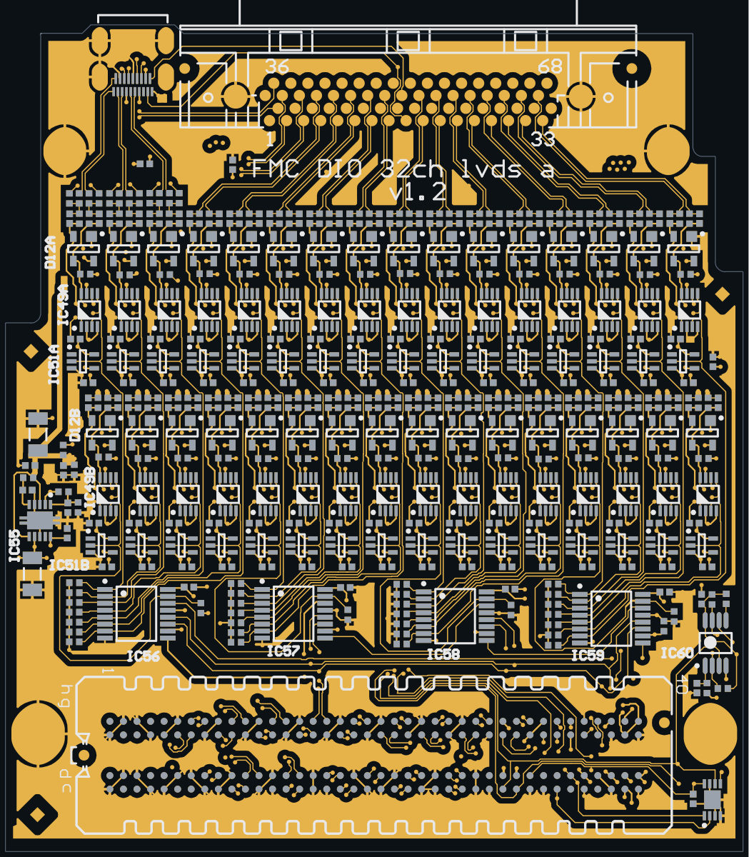
FMC DIO 32CHLVDSA (OHWR0040 R1) is an open-hardware circuit board from the CERN Open Hardware Repository, designed in Altium Designer: a 4-layer board of 69.1 × 77.5 mm with 558 components and 349 nets, published under CERN-OHL-1.1.
review 61% walked · 13 findings: 5 major · 8 minor (15 items)
Open in the interactive viewerRead the full review
Design review
Probe recorded 13 findings: 5 major · 8 minor (15 items) on this design. Each is shown here with its reasoning; the full review links every one to the pins, nets and datasheet pages it rests on.
TPS51200 REFOUT is tied to VO on LVDS_REF, putting 25 uF on a reference output rated for 0.47 uF
The TPS51200 IC55 has REFOUT tied to VO on LVDS_REF, which puts 25.4 µF on a reference output rated for 0.47 µF and leaves VO regulating to its own output.
Where it is
IC55 has VO (pin 3) and REFOUT (pin 6) both on net LVDS_REF; VOSNS (pin 5) reaches LVDS_REF through R252 10 Ω. The rail value is 1.65 V, from R251/R253 10k/10k.
The numbers
Quantity Value Source C147 22 µF, 1206 X7R 10 V netlist: LVDS_REF C151, C152 100 nF each netlist: LVDS_REF C139x, 32 channel parts 100 nF each netlist: LVDS_REF Total on LVDS_REF 25.4 µF derived REFOUT capacitance limit 'keep total capacitance on REFOUT pin below 0.47 µF' TPS51200 datasheet, p.3 Ratio to the REFOUT limit about 54 times derived VO minimum output capacitance 20 µF TPS51200 datasheet, p.1 VO regulation 'The output voltage, VO, is regulated to REFOUT' TPS51200 datasheet, p.10 With the two pins tied, VO has its own output as its reference, and the node is held only by the 10 mA REFOUT buffer.
Why it matters
The intended TPS51200 connection is REFOUT to GND through 0.1 µF on its own, and VO with at least 20 µF feeding the load, sensed by VOSNS. The two requirements cannot both be met on one node, so the part is outside its datasheet conditions: REFOUT stability is not assured, and the 3 A VO stage no longer regulates LVDS_REF.
Suggested fix: separate REFOUT (0.1 µF) from VO/LVDS_REF.
- DecapViaFanoutmajorOpen
DecapViaFanout: 2 components×2
Checked by the review, stands · Claude walker W3 (Cern session) — Checked: the fan-out length is read from the copper as stated. The 0.5 nH limit is Probe's starting value, not a datasheet or vendor requirement on file; whether it matters depends on this capacitor's role in the rail's PDN target. Left for the owner.
At C139C, C151
Each finding, with its own headline
C139CC139C on 'LVDS_REF': its rail pad reaches its via over 3.37 mm of track, adding about 0.93 nH to its loop, past Probe's 0.5 nH starting value; put the vias at the pads
C139C on 'LVDS_REF': its rail pad reaches its via over 3.37 mm of track, adding about 0.93 nH to its loop, past Probe's 0.5 nH starting value; put the vias at the pads. C139C.2 (rail) runs 3.37 mm along its copper to its nearest via, 2.37 mm past the 1 mm beside the pad: 0.93 nH; C139C.1 (ground) not measured: the pad sits in a pour of its net on its own layer, which has no track length to measure. Each run past the pad as one conductor of a pair 0.90 mm apart (the pad pitch), 0.2 l ln(D/R) nH with R 0.127 mm (the track's width is not read): 0.93 nH in all. Put the vias at the pads (or in them), one per pad at least, the rail's and the ground's close together; the capacitor's own inductance as mounted is 1.15 nH (pad 0.07 nH + no via of the first net within 1 mm of its pad: the study's 0.6 nH per mm of 1.30 mm depth, ASSUMED). 0.5 nH is Probe's starting value, about the whole mounted inductance of a well-mounted 0402.
C151C151 on 'LVDS_REF': its rail pad reaches its via over 4.15 mm of track, adding about 1.23 nH to its loop, past Probe's 0.5 nH starting value; put the vias at the pads
C151 on 'LVDS_REF': its rail pad reaches its via over 4.15 mm of track, adding about 1.23 nH to its loop, past Probe's 0.5 nH starting value; put the vias at the pads. C151.2 (rail) runs 4.15 mm along its copper to its nearest via, 3.15 mm past the 1 mm beside the pad: 1.23 nH; C151.1 (ground) not measured: the pad sits in a pour of its net on its own layer, which has no track length to measure. Each run past the pad as one conductor of a pair 0.90 mm apart (the pad pitch), 0.2 l ln(D/R) nH with R 0.127 mm (the track's width is not read): 1.23 nH in all. Put the vias at the pads (or in them), one per pad at least, the rail's and the ground's close together; the capacitor's own inductance as mounted is 0.44 nH (pad 0.07 nH + no via of the first net within 1 mm of its pad: the study's 0.6 nH per mm of 0.11 mm depth, ASSUMED). 0.5 nH is Probe's starting value, about the whole mounted inductance of a well-mounted 0402.
- NetCopperSplitmajorOpen
GND's copper is in 2 pieces joined only through J41: J41.SHIELD is connected only if the part bonds its pins inside
GND's copper is in 2 pieces joined only through J41: J41.SHIELD is connected only if the part bonds its pins inside. Piece 1: B10.1, B11.1, B8.1, B9.1, C1.2, C127A.1, C127B.1, C127C.1 and 431 more pin(s), on TOP_LAYER and BOTTOM_LAYER, 233 drill(s), 2215.18 mm2 of pour, over (3.94, 6.19) to (71.94, 82.73). Piece 2: J41.SHIELD, on TOP_LAYER, over (17.67, 76.77) to (19.17, 79.32). Only J41 has pins in more than one piece; if those pins are bonded inside the package the net is whole, and if not, the copper leaves it open. A track or a via of the net joining the pieces closes it.
At split:GND
- ReferencePlaneDiscontinuitymajorOpen
ReferencePlaneDiscontinuity: 2 boards×2
Checked by the review, stands · Claude walker W3 (Cern session) — Checked: the reference break is read from the copper as stated. Whether it matters depends on the signal's edge rate and the receiver's margin, which no datasheet or app note on file fixes for this net; the impedance step and reflection figures are Probe's model, and the thresholds are its starting values. Layout practice, not a datasheet requirement. Left for the owner.
At refchange:GND|P3V3, split@G:LVDS_REF|P3V3
Each finding, with its own headline
refchange:GND|P3V3220 nets change reference between GND and P3V3 at 305 vias, none with a reference that continues across (fastest: CON1R1_N at 100 ps 10-90 %, ASSUMED)
At 305 via(s), on 220 net(s), the signal leaves a layer referenced by one of GND and P3V3 for a layer referenced by the other, and no plane references both layers. Different nets: no via can carry the return across; only decoupling between the two planes near the via can. The capacitor carrying the return across was measured at each via, at the knee of the crossing net's edge against 50 ohm assumed: 305 with none. 305 of them at an ASSUMED edge (no edge on file for the net): state one (net_timing_state) and it is re-read. One decision covers the pair: whether GND and P3V3 are decoupled to each other near these vias. A via whose layers have more references than these two is a site of each pair it joins. None is partial: at every one, no reference continues across the via.
- 'SDA_OUT' at (70.08, 25.78), TOP_LAYER -> BOTTOM_LAYER: P3V3 on G to GND on SUP; pure, no reference continues across; stitching none, 87.9 mm of track past the via on BOTTOM_LAYER: At the 5 GHz knee of a 100 ps edge (10 ns 10-90 %, assumed: no edge is on file for the net) no capacitor carries the return; only the planes do. GND and P3V3 are not a thin pair (at most 0.2 mm), so their own capacitance does not carry the return. To serve it, change layers across the same plane, or move the signal to a layer referenced to ground. None.
- 'SCL_OUT' at (40.14, 78.98), TOP_LAYER -> BOTTOM_LAYER: P3V3 on G to GND on SUP; pure, no reference continues across; stitching none, 82.5 mm of track past the via on BOTTOM_LAYER: At the 5 GHz knee of a 100 ps edge (10 ns 10-90 %, assumed: no edge is on file for the net) no capacitor carries the return; only the planes do. GND and P3V3 are not a thin pair (at most 0.2 mm), so their own capacitance does not carry the return. To serve it, change layers across the same plane, or move the signal to a layer referenced to ground. None.
- 'SCL_OUT' at (69.62, 24.09), TOP_LAYER -> BOTTOM_LAYER: P3V3 on G to GND on SUP; pure, no reference continues across; stitching none, 82.5 mm of track past the via on BOTTOM_LAYER: At the 5 GHz knee of a 100 ps edge (10 ns 10-90 %, assumed: no edge is on file for the net) no capacitor carries the return; only the planes do. GND and P3V3 are not a thin pair (at most 0.2 mm), so their own capacitance does not carry the return. To serve it, change layers across the same plane, or move the signal to a layer referenced to ground. None.
- 'FMC1_P31' at (55.4, 17.09), TOP_LAYER -> BOTTOM_LAYER: P3V3 on G to GND on SUP; pure, no reference continues across; stitching none, 54.0 mm of track past the via on BOTTOM_LAYER: At the 5 GHz knee of a 100 ps edge (100 ps 10-90 %, assumed: no edge is on file for the net) no capacitor carries the return; only the planes do. GND and P3V3 are not a thin pair (at most 0.2 mm), so their own capacitance does not carry the return. To serve it, change layers across the same plane, or move the signal to a layer referenced to ground. None.
- 'FMC1_P31' at (67.88, 56.79), TOP_LAYER -> BOTTOM_LAYER: P3V3 on G to GND on SUP; pure, no reference continues across; stitching none, 54.0 mm of track past the via on BOTTOM_LAYER: At the 5 GHz knee of a 100 ps edge (100 ps 10-90 %, assumed: no edge is on file for the net) no capacitor carries the return; only the planes do. GND and P3V3 are not a thin pair (at most 0.2 mm), so their own capacitance does not carry the return. To serve it, change layers across the same plane, or move the signal to a layer referenced to ground. None.
- 'FMC1_P27' at (60.38, 56.79), TOP_LAYER -> BOTTOM_LAYER: P3V3 on G to GND on SUP; pure, no reference continues across; stitching none, 54.0 mm of track past the via on BOTTOM_LAYER: At the 5 GHz knee of a 100 ps edge (100 ps 10-90 %, assumed: no edge is on file for the net) no capacitor carries the return; only the planes do. GND and P3V3 are not a thin pair (at most 0.2 mm), so their own capacitance does not carry the return. To serve it, change layers across the same plane, or move the signal to a layer referenced to ground. None.
- 'FMC1_P27' at (45.67, 12.14), TOP_LAYER -> BOTTOM_LAYER: P3V3 on G to GND on SUP; pure, no reference continues across; stitching none, 54.0 mm of track past the via on BOTTOM_LAYER: At the 5 GHz knee of a 100 ps edge (100 ps 10-90 %, assumed: no edge is on file for the net) no capacitor carries the return; only the planes do. GND and P3V3 are not a thin pair (at most 0.2 mm), so their own capacitance does not carry the return. To serve it, change layers across the same plane, or move the signal to a layer referenced to ground. Measured for reference: C162 (100 nF 0402) 1.9 mm away: 1.17 nH in the 1.080 mm cavity + 0.30 nH ESL + 1.41 nH mounting (pad 0.07 nH (vias beside the pads) + 1 via pair(s) at 1.66 mm pitch, 0.20 mm drill, 1.19 mm to the farther plane): 90.4 ohm at the knee, 181 % of 50 ohm (assumed track impedance). None.
- 'FMC1_N27' at (60.33, 55.93), TOP_LAYER -> BOTTOM_LAYER: P3V3 on G to GND on SUP; pure, no reference continues across; stitching none, 53.2 mm of track past the via on BOTTOM_LAYER: At the 5 GHz knee of a 100 ps edge (100 ps 10-90 %, assumed: no edge is on file for the net) no capacitor carries the return; only the planes do. GND and P3V3 are not a thin pair (at most 0.2 mm), so their own capacitance does not carry the return. To serve it, change layers across the same plane, or move the signal to a layer referenced to ground. None.
- 'FMC1_N27' at (45.64, 13.11), TOP_LAYER -> BOTTOM_LAYER: P3V3 on G to GND on SUP; pure, no reference continues across; stitching none, 53.2 mm of track past the via on BOTTOM_LAYER: At the 5 GHz knee of a 100 ps edge (100 ps 10-90 %, assumed: no edge is on file for the net) no capacitor carries the return; only the planes do. GND and P3V3 are not a thin pair (at most 0.2 mm), so their own capacitance does not carry the return. To serve it, change layers across the same plane, or move the signal to a layer referenced to ground. Measured for reference: C162 (100 nF 0402) 1.1 mm away: 0.95 nH in the 1.080 mm cavity + 0.30 nH ESL + 1.41 nH mounting (pad 0.07 nH (vias beside the pads) + 1 via pair(s) at 1.66 mm pitch, 0.20 mm drill, 1.19 mm to the farther plane): 83.4 ohm at the knee, 167 % of 50 ohm (assumed track impedance). None.
- 'FMC1_N31' at (56.36, 17.12), TOP_LAYER -> BOTTOM_LAYER: P3V3 on G to GND on SUP; pure, no reference continues across; stitching none, 52.8 mm of track past the via on BOTTOM_LAYER: At the 5 GHz knee of a 100 ps edge (100 ps 10-90 %, assumed: no edge is on file for the net) no capacitor carries the return; only the planes do. GND and P3V3 are not a thin pair (at most 0.2 mm), so their own capacitance does not carry the return. To serve it, change layers across the same plane, or move the signal to a layer referenced to ground. None.
- 'FMC1_N31' at (67.83, 55.93), TOP_LAYER -> BOTTOM_LAYER: P3V3 on G to GND on SUP; pure, no reference continues across; stitching none, 52.8 mm of track past the via on BOTTOM_LAYER: At the 5 GHz knee of a 100 ps edge (100 ps 10-90 %, assumed: no edge is on file for the net) no capacitor carries the return; only the planes do. GND and P3V3 are not a thin pair (at most 0.2 mm), so their own capacitance does not carry the return. To serve it, change layers across the same plane, or move the signal to a layer referenced to ground. None.
- 'FMC1_P19' at (40.41, 11.61), TOP_LAYER -> BOTTOM_LAYER: P3V3 on G to GND on SUP; pure, no reference continues across; stitching none, 51.7 mm of track past the via on BOTTOM_LAYER: At the 5 GHz knee of a 100 ps edge (100 ps 10-90 %, assumed: no edge is on file for the net) no capacitor carries the return; only the planes do. GND and P3V3 are not a thin pair (at most 0.2 mm), so their own capacitance does not carry the return. To serve it, change layers across the same plane, or move the signal to a layer referenced to ground. None.
- and 293 more
Every site is a row of this finding's evidence, keyed by net, layers and position. GET /api/odb/boards/41/reference-planes?group=refchange%3AGND%7CP3V3 serves each with its own layer_image region; all of them lie in x 7.98..73.5, y 8.77..81.72 mm (board frame, Y up).
The reference on each layer is the first plane the track meets leaving the via, anti-pads and the net's own copper skipped. Whether it matters depends on each signal's edge rate, which nothing on file states for these nets: a slow static line crosses a split harmlessly, a fast edge does not.
split@G:LVDS_REF|P3V379 nets cross the split between the LVDS_REF and P3V3 planes on G at 158 places, with no plane on the track's other side (fastest: NetC140A_2 at 100 ps 10-90 %, ASSUMED)
On G the LVDS_REF and P3V3 planes part, and 79 nets cross from one to the other at 158 place(s). The return current cannot follow a track across; it detours to wherever the two planes are joined (a stitching capacitor, or the source), and the loop it opens radiates and couples. One decision covers the boundary: whether it is stitched near these crossings, or the nets crossing it are slow enough not to care. Tracks that run ALONG this split, down the slot rather than across it, are a finding of their own: theirs is an impedance step, not a detour. At 0 of the 158 crossing(s) the track's other neighbour carries a plane, which the return can use there; 158 are on an outer layer, with no other neighbour. No crossing has a plane on the track's other side, so the whole return meets the break.
- 'EN1_RX1' on TOP_LAYER at (14.39, 44.93), 0.15 mm; other side: none: the signal layer is outermost
- 'EN1_RX1' on TOP_LAYER at (14.39, 45.72), 0.15 mm; other side: none: the signal layer is outermost
- 'EN1_RX11' on TOP_LAYER at (33.15, 44.93), 0.15 mm; other side: none: the signal layer is outermost
- 'EN1_RX11' on TOP_LAYER at (33.15, 45.72), 0.15 mm; other side: none: the signal layer is outermost
- 'EN1_RX13' on TOP_LAYER at (36.93, 44.93), 0.15 mm; other side: none: the signal layer is outermost
- 'EN1_RX13' on TOP_LAYER at (36.93, 45.72), 0.15 mm; other side: none: the signal layer is outermost
- 'EN1_RX15' on TOP_LAYER at (40.59, 44.93), 0.15 mm; other side: none: the signal layer is outermost
- 'EN1_RX15' on TOP_LAYER at (40.59, 45.72), 0.15 mm; other side: none: the signal layer is outermost
- 'EN1_RX17' on TOP_LAYER at (44.4, 44.93), 0.15 mm; other side: none: the signal layer is outermost
- 'EN1_RX17' on TOP_LAYER at (44.4, 45.72), 0.15 mm; other side: none: the signal layer is outermost
- 'EN1_RX19' on TOP_LAYER at (48.14, 45.74), 0.2 mm; other side: none: the signal layer is outermost
- 'EN1_RX19' on TOP_LAYER at (48.19, 44.93), 0.15 mm; other side: none: the signal layer is outermost
- and 146 more
Every site is a row of this finding's evidence, keyed by net, layers and position. GET /api/odb/boards/41/reference-planes?group=split%40G%3ALVDS_REF%7CP3V3 serves each with its own layer_image region; all of them lie in x 8.47..69.46, y 43.62..64.04 mm (board frame, Y up).
Read from the copper as drawn on the reference layer, along each track's centreline at exact breakpoints. The reference is the copper beside the track, never the layer's type or name. Whether it matters depends on each signal's edge rate, which nothing on file states for these nets: a slow static line crosses a split harmlessly, a fast edge does not.
- PartLifecyclemajorOpen
SN74LV595APWT on 4 placements (IC56, IC57, IC58, IC59): the distributor catalogue reports "Obsolete" for Texas Instruments's SN74LV595APWT
SN74LV595APWT on 4 placements (IC56, IC57, IC58, IC59): the distributor catalogue reports "Obsolete" for Texas Instruments's SN74LV595APWT — a sourcing/longevity risk to confirm against the MANUFACTURER before acting. This board's BOM names no manufacturer for it, so whether that is the fitted maker's product was not checked. A distributor delisting is not the same claim as the part being unavailable; check the vendor's own lifecycle/product-change notice for the status and any named successor. Re-read the source: GET /api/odb/parts/SN74LV595APWT/providers (which provider said it, the maker and part number it matched, its own words, and when we asked). THE LAST BUY DATE HAS PASSED (2024-01-31, 1,019 day(s) ago), so this is a substitution rather than a buy. The distributor reports NONE left. No approved alternate is recorded for this position.
At IC56
LVDS line bias is 1.65 V, not the labelled 0.75 V, and above the FIN1101 driver offset voltage
The LVDS line bias LVDS_REF is 1.65 V, not the labelled 0.75 V, and a transmitting FIN1101 (IC50x) is pulled to it through the local termination, outside its 1.125-1.375 V specified offset.
Where it is
``
mermaid flowchart LR D["R251 10k from P3V3<br/>R253 10k to GND"] -- "REFIN 1.65 V" --> U["IC55 TPS51200"] U -- "LVDS_REF" --> R1["R1x 0 Ω"] R1 --> T["R244x/R245x 49.9 Ω<br/>termination midpoint"] T --- P["Channel pair<br/>IC50x FIN1101 out, IC49x in"]``Each channel splits its line termination (R244x/R245x 49.9 Ω) to LVDS_REF through R1x 0 Ω. The IC50x outputs (pins 5/6) and the IC49x inputs (pins 1/8) share that terminated pair.
The numbers
Quantity Value Source REFIN, and so LVDS_REF P3V3 x 10k / (10k + 10k) = 1.65 V netlist: R251, R253; derived Schematic label on VO and REFOUT 0.75V schematic sheet 2 FIN1101 offset voltage, min/typ/max 1.125 / 1.23 / 1.375 V FIN1101 datasheet, p.2 Current to hold 1.23 V against 1.65 V through 25 Ω about 17 mA derived FIN1101 short-circuit output current 3.4 to 6 mA FIN1101 datasheet, p.2 The driver cannot supply that current, so the line common mode is pulled near 1.65 V, outside the offset range.
Why it matters
A receiver-only bias would be harmless: 1.65 V is inside the FIN1101 input common-mode range. The problem is the shared bidirectional node. The local termination stays fitted in transmit, so the driver works outside its specified offset and every transmitting channel loads LVDS_REF.
The designer should state the intended bias (0.75 V label, 1.2 V LVDS, or 1.65 V) and whether the local termination should be switched out in transmit.
Channel direction is undefined from power-up: the SN74LV595 outputs are permanently enabled
Channel direction is undefined from power-up: the four SN74LV595 shift registers IC56-IC59 that set EN1_RX1-32 have their outputs permanently enabled, so the 47k pull-downs cannot act and some channels drive the cable until the FPGA loads a pattern.
Where it is
``
mermaid flowchart LR P["P3V3"] --> SR["IC56-IC59 SN74LV595<br/>OE pin 13 on GND<br/>SRCLR pin 10 on P3V3"] SR -- "EN1_RX1-32, R256-R307 47k to GND" --> RX["Receiver IC49x EN"] SR -- "EN1_RXn" --> INV["Inverter IC51x"] INV --> TX["Driver IC50x EN"]``- OE is active low (SN74LV595 datasheet, p.3) and tied to GND, and SRCLR is tied to P3V3. The outputs drive the channel enables from the moment P3V3 rises, with whatever the storage registers power up holding.
- EN_RX high enables the receiver IC49x and, through inverter IC51x, disables the driver IC50x (e.g. IC49A pin 3 takes EN1_RX1 directly; IC51A inverts it onto IC50A pin 3).
- The 47k pull-downs R256-R307 on every EN1_RXn cannot act against a driven output.
Each channel is receive or transmit at random until the FPGA shifts in a pattern and pulses LATCH.
Why it matters
The pull-downs show that a defined default was intended. It only works if OE is held high (pulled up to P3V3, released by the FPGA) until the register is loaded. As built, two boards cabled together can drive each other until both FPGAs are configured.
TXB0304 IC1: 10 k pull-down on an I/O, below the 20 k minimum, and OE tied straight to VADJ
The TXB0304 translator IC1 has a 10k pull-down (R2) on an I/O, below the 20 kΩ minimum, and its OE tied straight to VADJ instead of through a pull-down.
Where it is
Pin Connection Datasheet rule Source A1, pin 2 (net LA32_P, drawn as LATCH_VADJ) R2 10k to GND external pull resistors 'must be kept higher than 20 kΩ to ensure that they do not contend with the output drivers of the TXB0304' TXB0304 datasheet, p.11 OE, pin 12 tied directly to VADJ 'OE should be tied to GND through a pull-down', holding the outputs in high impedance during power-up and power-down TXB0304 datasheet, p.1 VCCB, pin 11 P3V3 netlist: IC1 VCCA, pin 1 VADJ in the layout PCB The netlist shows VCCA open only because the footprint has a second pad also named 1.
Why it matters
LATCH is driven A to B by the FPGA, so in normal use R2 only loads the FPGA pin. But while the FPGA is unconfigured, the TXB one-shot and 4 k output stage on A1 contend with 10 k. With OE hard-wired, the B side follows floating A inputs as soon as both rails are up.
Suggested fix: a 47k-100k pull-down, and OE pulled low and driven by the FPGA, would meet the datasheet.
Schematic annotations are stale: 0.75V labels on a 1.65 V rail, a note naming a part not on the board, unfilled title blocks
Several schematic annotations are stale: 0.75V labels on a rail set to 1.65 V, a placement note naming a part not on the board, and unfilled title blocks.
What is stale
- Sheet 2, IC55 TPS51200: the VO and REFOUT nets are labelled 0.75V (green text), but R251/R253 10k/10k (P3V3 to REFIN, REFIN to GND) set REFIN, and so LVDS_REF, to 1.65 V.
- Sheet 3, IC62: the note reads "Place MCP9801 close to SN74BCT25245"; no SN74BCT25245 is on this board.
- Title blocks: every one shows Rev "-" and check date "XX/XX/XXXX" (Check.by MK), and all 32 buffer sheets print the same sheet number (29 of 29).
Why it matters
The 0.75 V figure is the DDR3 VTT value from the TPS51200 reference design and misleads anyone checking the LVDS bias. The placement note was copied from another design and leaves the intended sensor location unstated.
Suggested fix: correct the labels, the note and the revision fields so the published documentation matches the board.
Channels 27-32 have punctuation refdes in the PCB and BOM but AA-AF on the schematic
For channels 27-32 the PCB and the published BOM use punctuation refdes suffixes (
IC49[... `IC49``) where the schematic uses AA-AF: 84 designators do not cross-reference, and several break common tool chains.The mismatch
The buffer sheet is repeated 32 times, annotated A-Z and then AA-AF on the schematic (sheets 30-35). The PCB and BOM continue with the ASCII characters after Z:
Channels 27-32 Example Schematic (sheets 30-35) suffixes AA-AF IC49AA,D12AA,R244AAon sheet 30;IC49AFon sheet 35PCB and published BOM the ASCII characters after Z: [\]^_`IC49[(channel 27); `D12`,R1`,C139`` (channel 32)The six IC49 designators in the PCB and BOM are
IC49[,IC49\,IC49],IC49^,IC49_, `IC49``.Each of the six channels carries 14 affected parts, 84 designators in all: C127, C128, C139, C140, C141, D12, IC49, IC50, IC51, R1, R243, R244, R245, R246.
Why it matters
The schematic and the assembly data disagree for six channels, so a technician cannot cross-reference them. Backslash and backtick designators also break many pick-and-place, CSV and silkscreen tool chains.
Suggested fix: set the channel naming in the PCB to a two-letter or numeric suffix, which fixes both.
Micro-HDMI J41 is a non-HDMI port: 3.3 V on the +5V contact and LVDS on the TMDS pairs, so a real HDMI device back-feeds P3V3
The micro-HDMI receptacle J41 is a private LVDS port, not HDMI: its +5V contact 19 is fed from P3V3 and its TMDS pairs carry LVDS, so a real HDMI source plugged in by mistake back-feeds the 3.3 V FMC rail.
How the contacts are used
J41 is an HDMI Type D receptacle (Molex 46765-1001).
J41 contacts HDMI 1.4 Type D role Used here for 3/5, 6/8, 9/11, 12/14 TMDS Data2, Data1, Data0 and Clock pairs LVDS 19 +5V power, driven by an HDMI source fed from P3V3 through PTC F6 (0.14 A hold), net NetF6_2 LVDS channels 1-5 (CON1_P1-P5 / CON1_N1-N5, routed through R265-R288 0 Ω to the J41 pairs as well as to J42) sit on the TMDS and HPD/utility pairs. The J41 pin names are 1/2 HEAC_N/P, 3/5 DATA2_P/N, 6/8 DATA1_P/N, 9/11 DATA0_P/N, 12/14 CLK_P/N and 17/18 SCL_OUT/SDA_OUT.
What happens with an HDMI source
``
mermaid flowchart LR S["HDMI source<br/>plugged in by mistake"] -- "about 5 V on contact 19" --> J["J41 pin 19<br/>NetF6_2"] J -- "back-feed until the PTC trips" --> F["F6 PTC<br/>0.14 A hold"] F --> P["P3V3<br/>3.3 V FMC rail"] S -- "TMDS outputs" --> L["FIN1101 LVDS I/O"]``Why it matters
Using a cheap, well-shielded HDMI cable for LVDS is a sound choice, but the receptacle invites a standard HDMI cable to a standard HDMI device.
Suggested fix: mark the front panel, and fit a series Schottky or ideal diode on contact 19 (or leave it unpowered) so a 5 V source cannot back-drive P3V3.
No HDMI requirement rows can be filed for this connector because the port is not HDMI.
- ReferencePlaneDiscontinuityminorOpen
'SDA_OUT' crosses one void in the GND plane on SUP at 1 place, the longest 5.02 mm (fastest: SDA_OUT at 10 ns 10-90 %, suggested by its name)
Along 'SDA_OUT' on BOTTOM_LAYER, the GND plane on SUP has 5.02 mm under the track with no copper, at (69.56, 62.61), the same plane on both sides. No single drill's anti-pad and no landing explains it: a clearance is excused only when it holds a drill and is drawn round it, or the track ends in it on the net's own pad or via, or runs through its own via's clearance and no farther. The return current detours round the void. 1 of them run ALONG the bare copper, parallel to its edges, rather than across it (the longest 4.25 mm). What cleared it: the hole at x 69.39..70.41, y 60.24..71.06. One decision covers the void: whether these tracks may cross it, or the plane should be filled under them. No crossing has a plane on the track's other side, so the whole return meets the break.
- 'SDA_OUT' on BOTTOM_LAYER at (69.56, 62.61), 5.02 mm, running ALONG the bare copper for 4.25 mm, not across it over no copper; other side: none: the signal layer is outermost
Every site is a row of this finding's evidence, keyed by net, layers and position. GET /api/odb/boards/41/reference-planes?group=void%3AGND%40SUP%3Ahole%2069.39%2C60.24%7C70.41%2C71.06 serves each with its own layer_image region; all of them lie in x 68.39..70.56, y 59.05..66.01 mm (board frame, Y up).
Read from the copper as drawn on the reference layer, along each track's centreline at exact breakpoints. The reference is the copper beside the track, never the layer's type or name. Whether it matters depends on each signal's edge rate, which nothing on file states for these nets: a slow static line crosses a split harmlessly, a fast edge does not.
At void:GND@SUP:hole 69.39,60.24|70.41,71.06
- DecapViaFanoutminorOpen
C147 on 'LVDS_REF': its rail pad reaches its via over 3.05 mm of track, adding about 1.30 nH to its loop, past Probe's 0.5 nH starting value; put the vias at the pads (a 22 uF bulk capacitor: its inductance matters only far above the band it serves)
C147 on 'LVDS_REF': its rail pad reaches its via over 3.05 mm of track, adding about 1.30 nH to its loop, past Probe's 0.5 nH starting value; put the vias at the pads (a 22 uF bulk capacitor: its inductance matters only far above the band it serves). C147.2 (rail) runs 3.05 mm along its copper to its nearest via, 2.05 mm past the 1 mm beside the pad: 1.30 nH; C147.1 (ground) not measured: the pad sits in a pour of its net on its own layer, which has no track length to measure. Each run past the pad as one conductor of a pair 3.00 mm apart (the pad pitch), 0.2 l ln(D/R) nH with R 0.127 mm (the track's width is not read): 1.30 nH in all. Put the vias at the pads (or in them), one per pad at least, the rail's and the ground's close together; the capacitor's own inductance as mounted is 1.07 nH (pad 0.20 nH + no via of the first net within 1 mm of its pad: the study's 0.6 nH per mm of 0.11 mm depth, ASSUMED). 0.5 nH is Probe's starting value, about the whole mounted inductance of a well-mounted 0402.
At C147
Main parts
| Part number | Maker | Description | Where |
|---|---|---|---|
| 24AA64T-I/MC | 1.7-5.5V 64K I2C Serial EEPROM | IC61 | |
| 46765-1001 | Molex | Connector HDMI 19 Male + 1 Shield | J41 |
| ASP-127797-01 | Samtec | Connector VITA 57, 160 Male contacts in 4 row cdgh | J40 |
| MCP9801-M/MS | 2-Wire High-Accuracy Temperature Sensor | IC62 | |
| TCA4311ADGKR | HOT SWAPPABLE 2-WIRE BUS BUFFERS | IC60 | |
| TPS51200DRCT | Sink/Source DDR Termination Regulator | IC55 | |
| TXB0304RUTR | 4-bit Bidirectional Auto-direction Sensing Translator with Fully Symmetric 0.9V to 3.6V Range | IC1 | |
| MINISMDC014F-2 | TE Connectivity | Resettable PTC fuse, 0.14 A hold, 60 V, 1812; schematic value "140mA-60V", library part FUSR1812_TYCO-MINISMDC014F | F6, F7 |
| SN74LV595APWT | 8-Bit Shift Register With 3-State Output Register | IC56, IC57, IC58, IC59 | |
| 74AHC1G04GW | Single Inverter Buffer | IC51A, IC51B, IC51C, IC51D, IC51E, IC51F and 26 more | |
| PRTR5V0U2X | Ultra Low Capacitance Double Rail-to-Rail ESD Protection Diode | D12A, D12B, D12C, D12D, D12E, D12F and 26 more | |
| FIN1101K8X | LVDS TO LVDS repeater3.3V | IC49A, IC49B, IC49C, IC49D, IC49E, IC49F and 58 more |
About this design
- Design
- FMC DIO 32CHLVDSA — OHWR0040 R1
- Designed in
- Altium Designer
- Board
- 4 copper layers, 69.1 × 77.5 mm, 558 components, 349 nets
- Licence
- CERN-OHL-1.1
- Source
- https://gitlab.com/ohwr/project/fmc-dio-32chlvdsa at commit
2a095492f107 - Attribution
- CERN Open Hardware Repository, project ohwr/project/fmc-dio-32chlvdsa (commit 2a095492f10742d0817181dd00b35c36995d4bfe, 2025-04-09). Licence: CERN-OHL-1.1. Source: https://gitlab.com/ohwr/project/fmc-dio-32chlvdsa. This is a snapshot of the copy published on the OHWR GitLab pages (R1), not CERN's released record. CERN's source of truth is EDMS (https://edms.cern.ch), and the current release may be newer.
- Reviewed with
- Probe by E# (E-Sharp AB)