 Probe

FMC DIO 32CHTTLA
OHWR0023 · revision R1
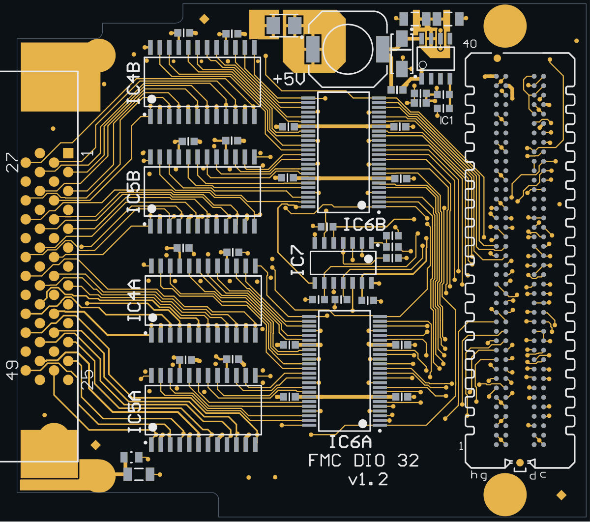
FMC DIO 32CHTTLA (OHWR0023 R1) is an open-hardware circuit board from the CERN Open Hardware Repository, designed in Altium Designer: a 4-layer board of 76.5 × 69 mm with 197 components and 183 nets, published under CERN-OHL-1.1.
review 83% walked · 7 findings: 1 blocker · 3 major · 3 minor (12 items)
Open in the interactive viewerRead the full review
Design review
Probe recorded 7 findings: 1 blocker · 3 major · 3 minor (12 items) on this design. Each is shown here with its reasoning; the full review links every one to the pins, nets and datasheet pages it rests on.
- NetCopperSplitblockerOpen
FRONT_PANEL2's copper is in 2 pieces: CON2.52 is not connected to the rest of the net
FRONT_PANEL2's copper is in 2 pieces: CON2.52 is not connected to the rest of the net. Piece 1: B3.1, B4.1, C2.1 and R25.2, on TOP_LAYER and BOTTOM_LAYER, 2 drill(s), 22.29 mm2 of pour, over (68.2, 67.9) to (136.3, 76.52). Piece 2: CON2.52, on TOP_LAYER and BOTTOM_LAYER, 1 drill(s), over (68.28, 73) to (76, 80.45). The export files every one of these pins under the net, so every connectivity check passes; the copper the fab builds leaves them apart. Usually a pour island that touches only one via of its own net, or a track ending short of its copper: join the piece to the net and export again.
At split:FRONT_PANEL2
- ReferencePlaneDiscontinuitymajorOpen
34 nets change reference between 5P0V and GND at 39 vias, none with a reference that continues across (fastest: DIO_0 at 100 ps 10-90 %, ASSUMED)
At 39 via(s), on 34 net(s), the signal leaves a layer referenced by one of 5P0V and GND for a layer referenced by the other, and no plane references both layers. Different nets: no via can carry the return across; only decoupling between the two planes near the via can. The capacitor carrying the return across was measured at each via, at the knee of the crossing net's edge against 50 ohm assumed: 39 with none. 39 of them at an ASSUMED edge (no edge on file for the net): state one (net_timing_state) and it is re-read. One decision covers the pair: whether 5P0V and GND are decoupled to each other near these vias. A via whose layers have more references than these two is a site of each pair it joins. None is partial: at every one, no reference continues across the via.
- 'DIR1' at (84.46, 86.36), TOP_LAYER -> BOTTOM_LAYER: GND on PLANE_L2_GND to 5P0V on PWR; pure, no reference continues across; stitching none, 35.6 mm of track past the via on BOTTOM_LAYER: At the 5 GHz knee of a 100 ps edge (100 ps 10-90 %, assumed: no edge is on file for the net) no capacitor carries the return; only the planes do. 5P0V and GND are not a thin pair (at most 0.2 mm), so their own capacitance does not carry the return. To serve it, change layers across the same plane, or move the signal to a layer referenced to ground. None.
- 'DIR3' at (84.84, 115.7), TOP_LAYER -> BOTTOM_LAYER: GND on PLANE_L2_GND to 5P0V on PWR; pure, no reference continues across; stitching none, 35.5 mm of track past the via on BOTTOM_LAYER: At the 5 GHz knee of a 100 ps edge (100 ps 10-90 %, assumed: no edge is on file for the net) no capacitor carries the return; only the planes do. 5P0V and GND are not a thin pair (at most 0.2 mm), so their own capacitance does not carry the return. To serve it, change layers across the same plane, or move the signal to a layer referenced to ground. None.
- 'DIR3' at (103.89, 109.35), TOP_LAYER -> BOTTOM_LAYER: GND on PLANE_L2_GND to 5P0V on PWR; pure, no reference continues across; stitching none, 35.5 mm of track past the via on BOTTOM_LAYER: At the 5 GHz knee of a 100 ps edge (100 ps 10-90 %, assumed: no edge is on file for the net) no capacitor carries the return; only the planes do. 5P0V and GND are not a thin pair (at most 0.2 mm), so their own capacitance does not carry the return. To serve it, change layers across the same plane, or move the signal to a layer referenced to ground. None.
- 'DIR2' at (84.84, 101.73), TOP_LAYER -> BOTTOM_LAYER: GND on PLANE_L2_GND to 5P0V on PWR; pure, no reference continues across; stitching none, 29.3 mm of track past the via on BOTTOM_LAYER: At the 5 GHz knee of a 100 ps edge (100 ps 10-90 %, assumed: no edge is on file for the net) no capacitor carries the return; only the planes do. 5P0V and GND are not a thin pair (at most 0.2 mm), so their own capacitance does not carry the return. To serve it, change layers across the same plane, or move the signal to a layer referenced to ground. None.
- 'DIR2' at (102.11, 101.35), TOP_LAYER -> BOTTOM_LAYER: GND on PLANE_L2_GND to 5P0V on PWR; pure, no reference continues across; stitching none, 29.3 mm of track past the via on BOTTOM_LAYER: At the 5 GHz knee of a 100 ps edge (100 ps 10-90 %, assumed: no edge is on file for the net) no capacitor carries the return; only the planes do. 5P0V and GND are not a thin pair (at most 0.2 mm), so their own capacitance does not carry the return. To serve it, change layers across the same plane, or move the signal to a layer referenced to ground. None.
- 'OE_N_1A' at (101.85, 86.74), TOP_LAYER -> BOTTOM_LAYER: GND on PLANE_L2_GND to 5P0V on PWR; pure, no reference continues across; stitching none, 24.6 mm of track past the via on BOTTOM_LAYER: At the 5 GHz knee of a 100 ps edge (100 ps 10-90 %, assumed: no edge is on file for the net) no capacitor carries the return; only the planes do. 5P0V and GND are not a thin pair (at most 0.2 mm), so their own capacitance does not carry the return. To serve it, change layers across the same plane, or move the signal to a layer referenced to ground. None.
- 'OE_N_1A' at (103.38, 80.14), TOP_LAYER -> BOTTOM_LAYER: GND on PLANE_L2_GND to 5P0V on PWR; pure, no reference continues across; stitching none, 24.6 mm of track past the via on BOTTOM_LAYER: At the 5 GHz knee of a 100 ps edge (100 ps 10-90 %, assumed: no edge is on file for the net) no capacitor carries the return; only the planes do. 5P0V and GND are not a thin pair (at most 0.2 mm), so their own capacitance does not carry the return. To serve it, change layers across the same plane, or move the signal to a layer referenced to ground. None.
- 'DIR4' at (84.96, 130.94), TOP_LAYER -> BOTTOM_LAYER: GND on PLANE_L2_GND to 5P0V on PWR; pure, no reference continues across; stitching none, 22.8 mm of track past the via on BOTTOM_LAYER: At the 5 GHz knee of a 100 ps edge (100 ps 10-90 %, assumed: no edge is on file for the net) no capacitor carries the return; only the planes do. 5P0V and GND are not a thin pair (at most 0.2 mm), so their own capacitance does not carry the return. To serve it, change layers across the same plane, or move the signal to a layer referenced to ground. None.
- 'DIR4' at (101.22, 129.79), TOP_LAYER -> BOTTOM_LAYER: GND on PLANE_L2_GND to 5P0V on PWR; pure, no reference continues across; stitching none, 22.8 mm of track past the via on BOTTOM_LAYER: At the 5 GHz knee of a 100 ps edge (100 ps 10-90 %, assumed: no edge is on file for the net) no capacitor carries the return; only the planes do. 5P0V and GND are not a thin pair (at most 0.2 mm), so their own capacitance does not carry the return. To serve it, change layers across the same plane, or move the signal to a layer referenced to ground. None.
- 'OE_N_2B' at (109.22, 124.08), TOP_LAYER -> BOTTOM_LAYER: GND on PLANE_L2_GND to 5P0V on PWR; pure, no reference continues across; stitching none, 15.2 mm of track past the via on BOTTOM_LAYER: At the 5 GHz knee of a 100 ps edge (100 ps 10-90 %, assumed: no edge is on file for the net) no capacitor carries the return; only the planes do. 5P0V and GND are not a thin pair (at most 0.2 mm), so their own capacitance does not carry the return. To serve it, change layers across the same plane, or move the signal to a layer referenced to ground. None.
- 'DIO_10' at (77.22, 96.52), TOP_LAYER -> BOTTOM_LAYER: GND on PLANE_L2_GND to 5P0V on PWR; pure, no reference continues across; stitching none, 9.8 mm of track past the via on BOTTOM_LAYER: At the 5 GHz knee of a 100 ps edge (100 ps 10-90 %, assumed: no edge is on file for the net) no capacitor carries the return; only the planes do. 5P0V and GND are not a thin pair (at most 0.2 mm), so their own capacitance does not carry the return. To serve it, change layers across the same plane, or move the signal to a layer referenced to ground. None.
- 'DIO_10' at (89.66, 93.6), TOP_LAYER -> BOTTOM_LAYER: GND on PLANE_L2_GND to 5P0V on PWR; pure, no reference continues across; stitching none, 9.8 mm of track past the via on BOTTOM_LAYER: At the 5 GHz knee of a 100 ps edge (100 ps 10-90 %, assumed: no edge is on file for the net) no capacitor carries the return; only the planes do. 5P0V and GND are not a thin pair (at most 0.2 mm), so their own capacitance does not carry the return. To serve it, change layers across the same plane, or move the signal to a layer referenced to ground. None.
- and 27 more
Every site is a row of this finding's evidence, keyed by net, layers and position. GET /api/odb/boards/26/reference-planes?group=refchange%3A5P0V%7CGND serves each with its own layer_image region; all of them lie in x 74.45..111.22, y 76.74..132.94 mm (board frame, Y up).
The reference on each layer is the first plane the track meets leaving the via, anti-pads and the net's own copper skipped. Whether it matters depends on each signal's edge rate, which nothing on file states for these nets: a slow static line crosses a split harmlessly, a fast edge does not.
At refchange:5P0V|GND
- PartLifecyclemajorOpen
PartLifecycle: 2 part numbers×2
2 Obsolete · on 3 placements
At IC6A, IC7
Each finding, with its own headline
IC6ASN74ALVTH162245DL on 2 placements (IC6A, IC6B): the distributor catalogue reports "Obsolete" for Texas Instruments's SN74ALVTH162245DL
SN74ALVTH162245DL on 2 placements (IC6A, IC6B): the distributor catalogue reports "Obsolete" for Texas Instruments's SN74ALVTH162245DL — a sourcing/longevity risk to confirm against the MANUFACTURER before acting. That is the maker this board's BOM names (TEXAS INSTRUMENTS). A distributor delisting is not the same claim as the part being unavailable; check the vendor's own lifecycle/product-change notice for the status and any named successor. Re-read the source: GET /api/odb/parts/SN74ALVTH162245DL/providers (which provider said it, the maker and part number it matched, its own words, and when we asked). THE LAST BUY DATE HAS PASSED (2023-04-22, 1,303 day(s) ago), so this is a substitution rather than a buy. The distributor reports 6,290 left. No approved alternate is recorded for this position.
IC7SN74HCT14D on IC7: the distributor catalogue reports "Obsolete" for Texas Instruments's SN74HCT14D
SN74HCT14D on IC7: the distributor catalogue reports "Obsolete" for Texas Instruments's SN74HCT14D — a sourcing/longevity risk to confirm against the MANUFACTURER before acting. That is the maker this board's BOM names (TEXAS INSTRUMENTS). A distributor delisting is not the same claim as the part being unavailable; check the vendor's own lifecycle/product-change notice for the status and any named successor. Re-read the source: GET /api/odb/parts/SN74HCT14D/providers (which provider said it, the maker and part number it matched, its own words, and when we asked). No approved alternate is recorded for this position.
- ReferencePlaneDiscontinuitymajorOpen
ReferencePlaneDiscontinuity: 4 boards×4
Checked by the review, stands · Claude walker W3 (Cern session) — Checked: the reference break is read from the copper as stated. Whether it matters depends on the signal's edge rate and the receiver's margin, which no datasheet or app note on file fixes for this net; the impedance step and reflection figures are Probe's model, and the thresholds are its starting values. Layout practice, not a datasheet requirement. Left for the owner.
At refchange:12P0V|GND, refchange:GND|VADJ, split@PWR:12P0V|VADJ, split@PWR:5P0V|VADJ
Each finding, with its own headline
refchange:12P0V|GND4 nets change reference between 12P0V and GND at 4 vias, none with a reference that continues across (fastest: GA0 at 100 ps 10-90 %, ASSUMED)
At 4 via(s), on 4 net(s), the signal leaves a layer referenced by one of 12P0V and GND for a layer referenced by the other, and no plane references both layers. Different nets: no via can carry the return across; only decoupling between the two planes near the via can. The capacitor carrying the return across was measured at each via, at the knee of the crossing net's edge against 50 ohm assumed: 4 with none. 4 of them at an ASSUMED edge (no edge on file for the net): state one (net_timing_state) and it is re-read. One decision covers the pair: whether 12P0V and GND are decoupled to each other near these vias. A via whose layers have more references than these two is a site of each pair it joins. None is partial: at every one, no reference continues across the via.
- 'GA0' at (139.57, 119.51), TOP_LAYER -> BOTTOM_LAYER: GND on PLANE_L2_GND to 12P0V on PWR; pure, no reference continues across; stitching none, 69.3 mm of track past the via on BOTTOM_LAYER: At the 5 GHz knee of a 100 ps edge (100 ps 10-90 %, assumed: no edge is on file for the net) no capacitor carries the return; only the planes do. 12P0V and GND are not a thin pair (at most 0.2 mm), so their own capacitance does not carry the return. To serve it, change layers across the same plane, or move the signal to a layer referenced to ground. None.
- 'GA1' at (139.57, 120.78), TOP_LAYER -> BOTTOM_LAYER: GND on PLANE_L2_GND to 12P0V on PWR; pure, no reference continues across; stitching none, 66.6 mm of track past the via on BOTTOM_LAYER: At the 5 GHz knee of a 100 ps edge (100 ps 10-90 %, assumed: no edge is on file for the net) no capacitor carries the return; only the planes do. 12P0V and GND are not a thin pair (at most 0.2 mm), so their own capacitance does not carry the return. To serve it, change layers across the same plane, or move the signal to a layer referenced to ground. None.
- 'SCL' at (139.63, 114.36), TOP_LAYER -> BOTTOM_LAYER: GND on PLANE_L2_GND to 12P0V on PWR; pure, no reference continues across; stitching none, 61.3 mm of track past the via on BOTTOM_LAYER: At the 5 GHz knee of a 100 ps edge (10 ns 10-90 %, assumed: no edge is on file for the net) no capacitor carries the return; only the planes do. 12P0V and GND are not a thin pair (at most 0.2 mm), so their own capacitance does not carry the return. To serve it, change layers across the same plane, or move the signal to a layer referenced to ground. None.
- 'SDA' at (140.18, 115.62), TOP_LAYER -> BOTTOM_LAYER: GND on PLANE_L2_GND to 12P0V on PWR; pure, no reference continues across; stitching none, 56.4 mm of track past the via on BOTTOM_LAYER: At the 5 GHz knee of a 100 ps edge (10 ns 10-90 %, assumed: no edge is on file for the net) no capacitor carries the return; only the planes do. 12P0V and GND are not a thin pair (at most 0.2 mm), so their own capacitance does not carry the return. To serve it, change layers across the same plane, or move the signal to a layer referenced to ground. None.
Every site is a row of this finding's evidence, keyed by net, layers and position. GET /api/odb/boards/26/reference-planes?group=refchange%3A12P0V%7CGND serves each with its own layer_image region; all of them lie in x 137.57..142.18, y 112.36..122.78 mm (board frame, Y up).
The reference on each layer is the first plane the track meets leaving the via, anti-pads and the net's own copper skipped. Whether it matters depends on each signal's edge rate, which nothing on file states for these nets: a slow static line crosses a split harmlessly, a fast edge does not.
refchange:GND|VADJ48 nets change reference between GND and VADJ at 89 vias, none with a reference that continues across (fastest: DIR1 at 100 ps 10-90 %, ASSUMED)
At 89 via(s), on 48 net(s), the signal leaves a layer referenced by one of GND and VADJ for a layer referenced by the other, and no plane references both layers. Different nets: no via can carry the return across; only decoupling between the two planes near the via can. The capacitor carrying the return across was measured at each via, at the knee of the crossing net's edge against 50 ohm assumed: 89 with none. 89 of them at an ASSUMED edge (no edge on file for the net): state one (net_timing_state) and it is re-read. One decision covers the pair: whether GND and VADJ are decoupled to each other near these vias. A via whose layers have more references than these two is a site of each pair it joins. None is partial: at every one, no reference continues across the via.
- 'SCL' at (135.08, 110.24), TOP_LAYER -> BOTTOM_LAYER: GND on PLANE_L2_GND to VADJ on PWR; pure, no reference continues across; stitching none, 61.3 mm of track past the via on BOTTOM_LAYER: At the 5 GHz knee of a 100 ps edge (10 ns 10-90 %, assumed: no edge is on file for the net) no capacitor carries the return; only the planes do. GND and VADJ are not a thin pair (at most 0.2 mm), so their own capacitance does not carry the return. To serve it, change layers across the same plane, or move the signal to a layer referenced to ground. None.
- 'NetCON2_26' at (112.9, 102.36), TOP_LAYER -> BOTTOM_LAYER: GND on PLANE_L2_GND to VADJ on PWR; pure, no reference continues across; stitching none, 57.8 mm of track past the via on BOTTOM_LAYER: At the 5 GHz knee of a 100 ps edge (100 ps 10-90 %, assumed: no edge is on file for the net) no capacitor carries the return; only the planes do. GND and VADJ are not a thin pair (at most 0.2 mm), so their own capacitance does not carry the return. To serve it, change layers across the same plane, or move the signal to a layer referenced to ground. None.
- 'SDA' at (134.27, 110.77), TOP_LAYER -> BOTTOM_LAYER: GND on PLANE_L2_GND to VADJ on PWR; pure, no reference continues across; stitching none, 56.4 mm of track past the via on BOTTOM_LAYER: At the 5 GHz knee of a 100 ps edge (10 ns 10-90 %, assumed: no edge is on file for the net) no capacitor carries the return; only the planes do. GND and VADJ are not a thin pair (at most 0.2 mm), so their own capacitance does not carry the return. To serve it, change layers across the same plane, or move the signal to a layer referenced to ground. None.
- 'NetIC7_4' at (111.63, 103.38), TOP_LAYER -> BOTTOM_LAYER: GND on PLANE_L2_GND to VADJ on PWR; pure, no reference continues across; stitching none, 54.5 mm of track past the via on BOTTOM_LAYER: At the 5 GHz knee of a 100 ps edge (100 ps 10-90 %, assumed: no edge is on file for the net) no capacitor carries the return; only the planes do. GND and VADJ are not a thin pair (at most 0.2 mm), so their own capacitance does not carry the return. To serve it, change layers across the same plane, or move the signal to a layer referenced to ground. None.
- 'NetIC7_2' at (114.17, 103), TOP_LAYER -> BOTTOM_LAYER: GND on PLANE_L2_GND to VADJ on PWR; pure, no reference continues across; stitching none, 52.9 mm of track past the via on BOTTOM_LAYER: At the 5 GHz knee of a 100 ps edge (100 ps 10-90 %, assumed: no edge is on file for the net) no capacitor carries the return; only the planes do. GND and VADJ are not a thin pair (at most 0.2 mm), so their own capacitance does not carry the return. To serve it, change layers across the same plane, or move the signal to a layer referenced to ground. None.
- 'DIR1' at (107.32, 78.87), TOP_LAYER -> BOTTOM_LAYER: GND on PLANE_L2_GND to VADJ on PWR; pure, no reference continues across; stitching none, 35.6 mm of track past the via on BOTTOM_LAYER: At the 5 GHz knee of a 100 ps edge (100 ps 10-90 %, assumed: no edge is on file for the net) no capacitor carries the return; only the planes do. GND and VADJ are not a thin pair (at most 0.2 mm), so their own capacitance does not carry the return. To serve it, change layers across the same plane, or move the signal to a layer referenced to ground. None.
- 'DIR1' at (125.22, 109.35), TOP_LAYER -> BOTTOM_LAYER: GND on PLANE_L2_GND to VADJ on PWR; pure, no reference continues across; stitching none, 35.6 mm of track past the via on BOTTOM_LAYER: At the 5 GHz knee of a 100 ps edge (100 ps 10-90 %, assumed: no edge is on file for the net) no capacitor carries the return; only the planes do. GND and VADJ are not a thin pair (at most 0.2 mm), so their own capacitance does not carry the return. To serve it, change layers across the same plane, or move the signal to a layer referenced to ground. None.
- 'DIR1' at (131.57, 109.35), TOP_LAYER -> BOTTOM_LAYER: GND on PLANE_L2_GND to VADJ on PWR; pure, no reference continues across; stitching none, 35.6 mm of track past the via on BOTTOM_LAYER: At the 5 GHz knee of a 100 ps edge (100 ps 10-90 %, assumed: no edge is on file for the net) no capacitor carries the return; only the planes do. GND and VADJ are not a thin pair (at most 0.2 mm), so their own capacitance does not carry the return. To serve it, change layers across the same plane, or move the signal to a layer referenced to ground. None.
- 'DIR3' at (122.94, 107.95), TOP_LAYER -> BOTTOM_LAYER: GND on PLANE_L2_GND to VADJ on PWR; pure, no reference continues across; stitching none, 35.5 mm of track past the via on BOTTOM_LAYER: At the 5 GHz knee of a 100 ps edge (100 ps 10-90 %, assumed: no edge is on file for the net) no capacitor carries the return; only the planes do. GND and VADJ are not a thin pair (at most 0.2 mm), so their own capacitance does not carry the return. To serve it, change layers across the same plane, or move the signal to a layer referenced to ground. None.
- 'DIR3' at (134.24, 107.95), TOP_LAYER -> BOTTOM_LAYER: GND on PLANE_L2_GND to VADJ on PWR; pure, no reference continues across; stitching none, 35.5 mm of track past the via on BOTTOM_LAYER: At the 5 GHz knee of a 100 ps edge (100 ps 10-90 %, assumed: no edge is on file for the net) no capacitor carries the return; only the planes do. GND and VADJ are not a thin pair (at most 0.2 mm), so their own capacitance does not carry the return. To serve it, change layers across the same plane, or move the signal to a layer referenced to ground. None.
- 'DIR2' at (122.94, 107.19), TOP_LAYER -> BOTTOM_LAYER: GND on PLANE_L2_GND to VADJ on PWR; pure, no reference continues across; stitching none, 29.3 mm of track past the via on BOTTOM_LAYER: At the 5 GHz knee of a 100 ps edge (100 ps 10-90 %, assumed: no edge is on file for the net) no capacitor carries the return; only the planes do. GND and VADJ are not a thin pair (at most 0.2 mm), so their own capacitance does not carry the return. To serve it, change layers across the same plane, or move the signal to a layer referenced to ground. None.
- 'DIR2' at (134.37, 106.68), TOP_LAYER -> BOTTOM_LAYER: GND on PLANE_L2_GND to VADJ on PWR; pure, no reference continues across; stitching none, 29.3 mm of track past the via on BOTTOM_LAYER: At the 5 GHz knee of a 100 ps edge (100 ps 10-90 %, assumed: no edge is on file for the net) no capacitor carries the return; only the planes do. GND and VADJ are not a thin pair (at most 0.2 mm), so their own capacitance does not carry the return. To serve it, change layers across the same plane, or move the signal to a layer referenced to ground. None.
- and 77 more
Every site is a row of this finding's evidence, keyed by net, layers and position. GET /api/odb/boards/26/reference-planes?group=refchange%3AGND%7CVADJ serves each with its own layer_image region; all of them lie in x 103.28..142.08, y 76.87..112.77 mm (board frame, Y up).
The reference on each layer is the first plane the track meets leaving the via, anti-pads and the net's own copper skipped. Whether it matters depends on each signal's edge rate, which nothing on file states for these nets: a slow static line crosses a split harmlessly, a fast edge does not.
split@PWR:12P0V|VADJ2 nets cross the split between the 12P0V and VADJ planes on PWR at 2 places, with no plane on the track's other side (fastest: GA0 at 100 ps 10-90 %, ASSUMED)
On PWR the 12P0V and VADJ planes part, and 2 nets cross from one to the other at 2 place(s). The return current cannot follow a track across; it detours to wherever the two planes are joined (a stitching capacitor, or the source), and the loop it opens radiates and couples. One decision covers the boundary: whether it is stitched near these crossings, or the nets crossing it are slow enough not to care. Tracks that run ALONG this split, down the slot rather than across it, are a finding of their own: theirs is an impedance step, not a detour. At 0 of the 2 crossing(s) the track's other neighbour carries a plane, which the return can use there; 2 are on an outer layer, with no other neighbour. No crossing has a plane on the track's other side, so the whole return meets the break.
- 'GA0' on BOTTOM_LAYER at (135, 119.51), 0.25 mm; other side: none: the signal layer is outermost
- 'GA1' on BOTTOM_LAYER at (135, 119.18), 0.25 mm; other side: none: the signal layer is outermost
Every site is a row of this finding's evidence, keyed by net, layers and position. GET /api/odb/boards/26/reference-planes?group=split%40PWR%3A12P0V%7CVADJ serves each with its own layer_image region; all of them lie in x 133.87..136.13, y 118.18..120.51 mm (board frame, Y up).
Read from the copper as drawn on the reference layer, along each track's centreline at exact breakpoints. The reference is the copper beside the track, never the layer's type or name. Whether it matters depends on each signal's edge rate, which nothing on file states for these nets: a slow static line crosses a split harmlessly, a fast edge does not.
split@PWR:5P0V|VADJ11 nets cross the split between the 5P0V and VADJ planes on PWR at 16 places, with no plane on the track's other side (fastest: DIR1 at 100 ps 10-90 %, ASSUMED)
On PWR the 5P0V and VADJ planes part, and 11 nets cross from one to the other at 16 place(s). The return current cannot follow a track across; it detours to wherever the two planes are joined (a stitching capacitor, or the source), and the loop it opens radiates and couples. One decision covers the boundary: whether it is stitched near these crossings, or the nets crossing it are slow enough not to care. Tracks that run ALONG this split, down the slot rather than across it, are a finding of their own: theirs is an impedance step, not a detour. At 0 of the 16 crossing(s) the track's other neighbour carries a plane, which the return can use there; 16 are on an outer layer, with no other neighbour. No crossing has a plane on the track's other side, so the whole return meets the break.
- 'ALERTN' on BOTTOM_LAYER at (104.08, 95.69), 0.36 mm; other side: none: the signal layer is outermost
- 'ALERTN' on BOTTOM_LAYER at (107.26, 97.97), 0.32 mm; other side: none: the signal layer is outermost
- 'ALERTN' on BOTTOM_LAYER at (116.18, 101.09), 0.36 mm; other side: none: the signal layer is outermost
- 'DIR1' on BOTTOM_LAYER at (103.76, 78.87), 0.25 mm; other side: none: the signal layer is outermost
- 'GA0' on BOTTOM_LAYER at (108.97, 101.22), 0.36 mm; other side: none: the signal layer is outermost
- 'NetCON2_26' on BOTTOM_LAYER at (108.22, 101.24), 0.31 mm; other side: none: the signal layer is outermost
- 'NetIC7_2' on BOTTOM_LAYER at (106.74, 102.68), 0.25 mm; other side: none: the signal layer is outermost
- 'NetIC7_4' on BOTTOM_LAYER at (103.89, 106.68), 0.36 mm; other side: none: the signal layer is outermost
- 'OE_N_1A' on BOTTOM_LAYER at (103.76, 86.74), 0.25 mm; other side: none: the signal layer is outermost
- 'OE_N_1B' on BOTTOM_LAYER at (103.81, 109.93), 0.3 mm; other side: none: the signal layer is outermost
- 'OE_N_2B' on BOTTOM_LAYER at (109.35, 122.81), 0.25 mm; other side: none: the signal layer is outermost
- 'SCL' on BOTTOM_LAYER at (103.76, 92.74), 0.25 mm; other side: none: the signal layer is outermost
- and 4 more
Every site is a row of this finding's evidence, keyed by net, layers and position. GET /api/odb/boards/26/reference-planes?group=split%40PWR%3A5P0V%7CVADJ serves each with its own layer_image region; all of them lie in x 102.63..118.17, y 77.87..123.94 mm (board frame, Y up).
Read from the copper as drawn on the reference layer, along each track's centreline at exact breakpoints. The reference is the copper beside the track, never the layer's type or name. Whether it matters depends on each signal's edge rate, which nothing on file states for these nets: a slow static line crosses a split harmlessly, a fast edge does not.
No reference designators on silk for any passive or LED, either side - only the ten ICs are labelled
No passive or LED has a reference designator on the silkscreen, on either side: only the ten ICs are labelled.
- Top: designators only for IC1, IC4A/B, IC5A/B, IC6A/B and IC7. Around IC7 (region 102-125 × 95-110 mm), R21, R23, R26, R27, R28, R61 and R64 show only a bar between their pads.
- Bottom: only IC2 and IC3 are labelled; the ~140 bottom passives and LED1-LED3 carry no designator.
None of the ~190 resistors and capacitors, the inductor L1, the diode D1 or LED1-LED3 has a designator anywhere on the board. Each passive has only a bar between its pads.
- DecapViaFanoutminorOpen
C6 on '5P0V': its rail pad reaches its via over 2.18 mm of track and its ground pad over 1.04 mm, adding about 0.62 nH to its loop, past Probe's 0.5 nH starting value; put the vias at the pads (within a quarter of the starting value)
C6 on '5P0V': its rail pad reaches its via over 2.18 mm of track and its ground pad over 1.04 mm, adding about 0.62 nH to its loop, past Probe's 0.5 nH starting value; put the vias at the pads (within a quarter of the starting value). C6.2 (rail) runs 2.18 mm along its copper to its nearest via, 1.18 mm past the 1 mm beside the pad: 0.60 nH; C6.1 (ground) runs 1.04 mm along its copper to its nearest via, 0.04 mm past the 1 mm beside the pad: 0.02 nH. Each run past the pad as one conductor of a pair 1.60 mm apart (the pad pitch), 0.2 l ln(D/R) nH with R 0.127 mm (the track's width is not read): 0.62 nH in all. Put the vias at the pads (or in them), one per pad at least, the rail's and the ground's close together; the capacitor's own inductance as mounted is 1.00 nH (pad 0.10 nH + no via of the first net within 1 mm of its pad: the study's 0.6 nH per mm of 0.65 mm depth, ASSUMED). 0.5 nH is Probe's starting value, about the whole mounted inductance of a well-mounted 0402.
At C6
- ReferencePlaneDiscontinuityminorOpen
ReferencePlaneDiscontinuity: 2 boards×2
Checked by the review, stands · Claude walker W3 (Cern session) — Checked: the reference break is read from the copper as stated. Whether it matters depends on the signal's edge rate and the receiver's margin, which no datasheet or app note on file fixes for this net; the impedance step and reflection figures are Probe's model, and the thresholds are its starting values. Layout practice, not a datasheet requirement. Left for the owner.
At along@PWR:5P0V|VADJ, void:VADJ@PWR:hole 103.63,67.56|103.89,95.5
Each finding, with its own headline
along@PWR:5P0V|VADJ'GA1' runs ALONG the split between the 5P0V and VADJ planes on PWR at 1 place, the longest 5.89 mm; the impedance rises from 77 ohm to 79 ohm there at worst, 1 % of each edge reflected (fastest: GA1 at 100 ps 10-90 %, ASSUMED)
On PWR the 5P0V and VADJ planes part, and 'GA1' runs down the slot between them at 1 place(s), rather than across it. This is not a crossing: the return still follows the track, in the plane on its other side and in the slot's edges, so it does not detour. What changes is the track's own impedance. With the plane gone from under it on this side for that length, its field reaches further, to the slot's edges and to the next plane beyond, so its capacitance falls and its impedance rises; every edge travelling down it is partly reflected where it enters the stretch and again where it leaves, by (Z2 - Z1)/(Z2 + Z1). The longer the stretch against the edge's rise, the more of the edge sees the full step. A crossing is generally the worse fault; a mismatch is not free. Over solid plane each track is 77 ohm; along the slot 79 ohm, reflecting up to 1 % of each edge (a method-of-moments field solve of the cross-section, one dielectric; were the slot's edges to carry none of the return, up to 103 ohm). At every place the rise is within 10 %, the tolerance controlled impedance is commonly built to (the stackup states none), so the finding is the lower tier (info). One decision covers the split line's slot: whether these tracks may run down it, or should be moved over solid plane.
- 'GA1' on BOTTOM_LAYER at (112.4, 101.17), 6.25 mm, running ALONG the split for 5.89 mm, not across it, 77 ohm over solid plane, 79 ohm along it: 1 % of each edge reflected; other side: none: the signal layer is outermost
Every site is a row of this finding's evidence, keyed by net, layers and position. GET /api/odb/boards/26/reference-planes?group=along%40PWR%3A5P0V%7CVADJ serves each with its own layer_image region; all of them lie in x 108.37..116.52, y 100.09..102.35 mm (board frame, Y up).
Read from the copper as drawn on the reference layer, along each track's centreline at exact breakpoints. The reference is the copper beside the track, never the layer's type or name. Whether it matters depends on each signal's edge rate, which nothing on file states for these nets: a slow static line crosses a split harmlessly, a fast edge does not.
void:VADJ@PWR:hole 103.63,67.56|103.89,95.5'SDA' crosses one void in the VADJ plane on PWR at 1 place, the longest 0.07 mm (fastest: SDA at 10 ns 10-90 %, suggested by its name)
Along 'SDA' on BOTTOM_LAYER, the VADJ plane on PWR has 0.07 mm under the track with no copper, at (103.85, 94.35), running to the end of the track. No single drill's anti-pad and no landing explains it: a clearance is excused only when it holds a drill and is drawn round it, or the track ends in it on the net's own pad or via, or runs through its own via's clearance and no farther. The return current detours round the void. What cleared it: the hole at x 103.63..103.89, y 67.56..95.5. One decision covers the void: whether these tracks may cross it, or the plane should be filled under them. No crossing has a plane on the track's other side, so the whole return meets the break.
- 'SDA' on BOTTOM_LAYER at (103.85, 94.35), 0.07 mm over no copper, to the end of the track; other side: none: the signal layer is outermost
Every site is a row of this finding's evidence, keyed by net, layers and position. GET /api/odb/boards/26/reference-planes?group=void%3AVADJ%40PWR%3Ahole%20103.63%2C67.56%7C103.89%2C95.5 serves each with its own layer_image region; all of them lie in x 102.82..104.89, y 93.35..95.35 mm (board frame, Y up).
Read from the copper as drawn on the reference layer, along each track's centreline at exact breakpoints. The reference is the copper beside the track, never the layer's type or name. Whether it matters depends on each signal's edge rate, which nothing on file states for these nets: a slow static line crosses a split harmlessly, a fast edge does not.
Main parts
| Part number | Maker | Description | Where |
|---|---|---|---|
| 15MQ040NPbF | VISHAY INTERTECHNOLOGY, INC. | Schottky Diode | D1 |
| 24AA64T-I/MC | MICROCHIP TECHNOLOGY | 1.7-5.5V 64K I2C Serial EEPROM | IC2 |
| ASP-134488-01 | SAMTEC | Connector VITA 57, 160 Male contacts in 4 row cdgh | J2 |
| LEDRA3010-BW120 | LED (Maritex) | LED2 | |
| LEDRA3010-GYW120 | LED (Maritex) | LED3 | |
| LEDRA3010-RW120 | LED (Maritex) | LED1 | |
| MCP9801-M/MS | MICROCHIP TECHNOLOGIY | 2-Wire High-Accuracy Temperature Sensor | IC3 |
| MD5RP50F0L3 or 10250-55H3PC or 10250-55H3PL | Position Header, Horizontal, with Retention Leg AMPLIMITE 050 Series Il Connector. Type B | CON2 | |
| SN74HCT14D | TEXAS INSTRUMENTS | Hex Schmitt-Trigger Inverter | IC7 |
| TPS5420D | TEXAS INSTRUMENTS | 2A, Wide Input Range, Step-Down SWIFT Converter | IC1 |
| SN74ALVTH162245DL | TEXAS INSTRUMENTS | 16-Bit Bus Transceiver with 3-State Outputs | IC6A, IC6B |
| SN74BCT25245DW | TEXAS INSTRUMENTS | 25 Ohms Octal Bus Transceiver With 3-State Outputs | IC4A, IC4B, IC5A, IC5B |
| CC0603_10NF_50V_10%_X7R | GENERIC | Non-polarised capacitor | C1 |
| CTE3528-21_100UF_6.3V_10% | GENERIC | Polarised capacitor | C5 |
| MSS1038-333ML_LC | COILCRAFT | Inductor With Magnetic core | L1 |
| R0603_1K5_1%_0.1W_100PPM | GENERIC | Resistor - 1% | R3 |
| R0603_4K7_1%_0.1W_100PPM | GENERIC | Resistor - 1% | R1 |
| 1206GA220JAT9A | AVX | Non-polarised capacitor | C2, C7 |
| CC1206_4.7UF_16V_10%_X5R | GENERIC | Non-polarised capacitor | C3, C4 |
| R0805_1M_1%_0.125W_100PPM | GENERIC | Resistor - 1% | R2, R25 |
| R0603_750R_1%_0.1W_100PPM | GENERIC | Resistor - 1% | R24, R4, R63 |
| CC0603_100NF_50V_10%_X7R | GENERIC | Non-polarised capacitor | C10, C15, C20A, C20B, C21A, C21B and 14 more |
| CC0603_2.2NF_50V_10%_X7R | GENERIC | Non-polarised capacitor | C11A, C11B, C12A, C12B, C13A, C13B and 26 more |
| R0603_10K_1%_0.1W_100PPM | GENERIC | Resistor - 1% | R10A, R10B, R11A, R11B, R12A, R12B and 34 more |
| R0805_100R_1%_0.125W_100PPM | GENERIC | Resistor - 1% | R29A, R29B, R30A, R30B, R31A, R31B and 58 more |
About this design
- Design
- FMC DIO 32CHTTLA — OHWR0023 R1
- Designed in
- Altium Designer
- Board
- 4 copper layers, 76.5 × 69 mm, 197 components, 183 nets
- Licence
- CERN-OHL-1.1
- Source
- https://gitlab.com/ohwr/project/fmc-dio-32chttla at commit
b060883873af - Attribution
- CERN Open Hardware Repository, project ohwr/project/fmc-dio-32chttla (commit b060883873af80d7095ad320f5a839d4ff3d01c4, 2025-04-09). Licence: CERN-OHL-1.1. Source: https://gitlab.com/ohwr/project/fmc-dio-32chttla. This is a snapshot of the copy published on the OHWR GitLab pages (R1), not CERN's released record. CERN's source of truth is EDMS (https://edms.cern.ch), and the current release may be newer.
- Reviewed with
- Probe by E# (E-Sharp AB)