 Probe

FMC NANOFIP
OHWR0068 · revision R1
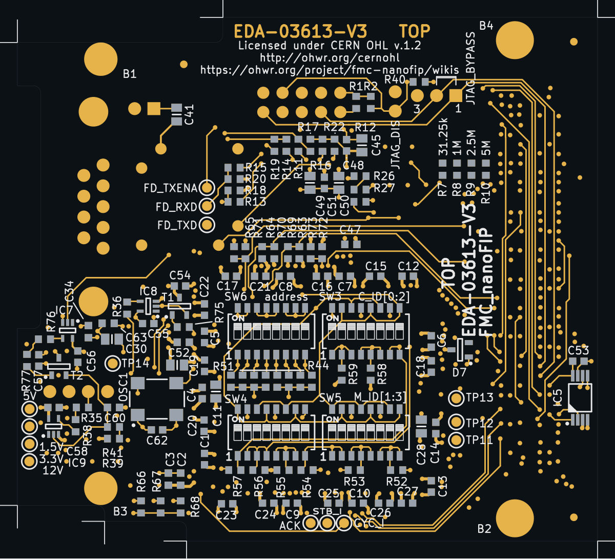
FMC NANOFIP (OHWR0068 R1) is an open-hardware circuit board from the CERN Open Hardware Repository, designed in KiCad EDA: a 8-layer board of 76.5 × 69 mm with 198 components and 251 nets, published under CERN-OHL-W-2.0.
review 86% walked · 17 findings: 7 major · 10 minor (30 items)
Open in the interactive viewerRead the full review
Design review
Probe recorded 17 findings: 7 major · 10 minor (30 items) on this design. Each is shown here with its reasoning; the full review links every one to the pins, nets and datasheet pages it rests on.
BZV49-C6V2,115 went end-of-life (Discontinued at DigiKey)
Vendor (DigiKey) lifecycle for BZV49-C6V2,115 (Nexperia USA Inc.'s listing) changed from "Active" to "Discontinued at DigiKey" since this board was reviewed. Placed as D6. A sourcing/longevity risk; consider a replacement before production.
- concernCON-001majorOpen
[eol:BZV49-C6V2,115:Discontinued at DigiKey] BZV49-C6V2,115 lifecycle changed from "Active" to "Discontinued at DigiKey" since this board was reviewed: OHWR0068 R1 FMC NANOFIP. A sourcing and longevity risk. Should this be replaced before the next build?
- ReferencePlaneDiscontinuitymajorOpen
'/Fieldbus/FIP_R_P' crosses where the outline of the GND plane on L7_GND is drawn back, at 1 place, the longest 0.55 mm (fastest: /Fieldbus/FIP_R_P at 100 ps 10-90 %, ASSUMED)
Along '/Fieldbus/FIP_R_P' on BOTTOM, the GND plane on L7_GND has 0.55 mm under the track with no copper, at (85.3, -240.46), running to the end of the track. No single drill's anti-pad and no landing explains it: a clearance is excused only when it holds a drill and is drawn round it, or the track ends in it on the net's own pad or via, or runs through its own via's clearance and no farther. The return current detours round the void. No hole cleared it: the outline of the pour at x 68.73..144.23, y -296..-228 is drawn back there. One decision covers the void: whether these tracks may cross it, or the plane should be filled under them. No crossing has a plane on the track's other side, so the whole return meets the break.
- '/Fieldbus/FIP_R_P' on BOTTOM at (85.3, -240.46), 0.55 mm over no copper, to the end of the track; other side: none: the signal layer is outermost
Every site is a row of this finding's evidence, keyed by net, layers and position. GET /api/odb/boards/69/reference-planes?group=void%3AGND%40L7_GND%3A85.3%2C-240.46 serves each with its own layer_image region; all of them lie in x 84.21..87.23, y -241.74..-238.52 mm (board frame, Y up).
Read from the copper as drawn on the reference layer, along each track's centreline at exact breakpoints. The reference is the copper beside the track, never the layer's type or name. Whether it matters depends on each signal's edge rate, which nothing on file states for these nets: a slow static line crosses a split harmlessly, a fast edge does not.
At void:GND@L7_GND:85.3,-240.46
- DecapViaFanoutmajorOpen
DecapViaFanout: 5 components×5
Checked by the review, stands · Claude walker W3 (Cern session) — Checked: the fan-out length is read from the copper as stated. The 0.5 nH limit is Probe's starting value, not a datasheet or vendor requirement on file; whether it matters depends on this capacitor's role in the rail's PDN target. Left for the owner.
At C2, C3, C51, C62, C8
Each finding, with its own headline
C2C2 on 'P3V3': its rail pad reaches its via over 0.00 mm of track and its ground pad over 2.82 mm, adding about 0.92 nH to its loop, past Probe's 0.5 nH starting value; put the vias at the pads
C2 on 'P3V3': its rail pad reaches its via over 0.00 mm of track and its ground pad over 2.82 mm, adding about 0.92 nH to its loop, past Probe's 0.5 nH starting value; put the vias at the pads. C2.1 (rail) runs 0.00 mm along its copper to its nearest via, beside the pad; C2.2 (ground) runs 2.82 mm along its copper to its nearest via, 1.82 mm past the 1 mm beside the pad: 0.92 nH. Each run past the pad as one conductor of a pair 1.60 mm apart (the pad pitch), 0.2 l ln(D/R) nH with R 0.127 mm (the track's width is not read): 0.92 nH in all. Put the vias at the pads (or in them), one per pad at least, the rail's and the ground's close together; the capacitor's own inductance as mounted is 1.07 nH (pad 0.10 nH + no via of the first net within 1 mm of its pad: the study's 0.6 nH per mm of 0.76 mm depth, ASSUMED). 0.5 nH is Probe's starting value, about the whole mounted inductance of a well-mounted 0402.
C3C3 on 'P3V3': its rail pad reaches its via over 3.63 mm of track and its ground pad over 1.20 mm, adding about 1.43 nH to its loop, past Probe's 0.5 nH starting value; put the vias at the pads
C3 on 'P3V3': its rail pad reaches its via over 3.63 mm of track and its ground pad over 1.20 mm, adding about 1.43 nH to its loop, past Probe's 0.5 nH starting value; put the vias at the pads. C3.1 (rail) runs 3.63 mm along its copper to its nearest via, 2.63 mm past the 1 mm beside the pad: 1.33 nH; C3.2 (ground) runs 1.20 mm along its copper to its nearest via, 0.20 mm past the 1 mm beside the pad: 0.10 nH. Each run past the pad as one conductor of a pair 1.60 mm apart (the pad pitch), 0.2 l ln(D/R) nH with R 0.127 mm (the track's width is not read): 1.43 nH in all. Put the vias at the pads (or in them), one per pad at least, the rail's and the ground's close together; the capacitor's own inductance as mounted is 1.07 nH (pad 0.10 nH + no via of the first net within 1 mm of its pad: the study's 0.6 nH per mm of 0.76 mm depth, ASSUMED). 0.5 nH is Probe's starting value, about the whole mounted inductance of a well-mounted 0402.
C51C51 on 'P5V': its rail pad reaches its via over 0.85 mm of track and its ground pad over 2.98 mm, adding about 0.98 nH to its loop, past Probe's 0.5 nH starting value; put the vias at the pads
C51 on 'P5V': its rail pad reaches its via over 0.85 mm of track and its ground pad over 2.98 mm, adding about 0.98 nH to its loop, past Probe's 0.5 nH starting value; put the vias at the pads. C51.1 (rail) runs 0.85 mm along its copper to its nearest via, beside the pad; C51.2 (ground) runs 2.98 mm along its copper to its nearest via, 1.98 mm past the 1 mm beside the pad: 0.98 nH. Each run past the pad as one conductor of a pair 1.50 mm apart (the pad pitch), 0.2 l ln(D/R) nH with R 0.127 mm (the track's width is not read): 0.98 nH in all. Put the vias at the pads (or in them), one per pad at least, the rail's and the ground's close together; the capacitor's own inductance as mounted is 0.84 nH (pad 0.10 nH + no via of the second net within 1 mm of its pad: the study's 0.6 nH per mm of 0.38 mm depth, ASSUMED). 0.5 nH is Probe's starting value, about the whole mounted inductance of a well-mounted 0402.
C62C62 on 'P3V3': its rail pad reaches its via over 1.31 mm of track and its ground pad over 2.03 mm, adding about 0.66 nH to its loop, past Probe's 0.5 nH starting value; put the vias at the pads
C62 on 'P3V3': its rail pad reaches its via over 1.31 mm of track and its ground pad over 2.03 mm, adding about 0.66 nH to its loop, past Probe's 0.5 nH starting value; put the vias at the pads. C62.1 (rail) runs 1.31 mm along its copper to its nearest via, 0.31 mm past the 1 mm beside the pad: 0.15 nH; C62.2 (ground) runs 2.03 mm along its copper to its nearest via, 1.03 mm past the 1 mm beside the pad: 0.51 nH. Each run past the pad as one conductor of a pair 1.50 mm apart (the pad pitch), 0.2 l ln(D/R) nH with R 0.127 mm (the track's width is not read): 0.66 nH in all. Put the vias at the pads (or in them), one per pad at least, the rail's and the ground's close together; the capacitor's own inductance as mounted is 1.07 nH (pad 0.10 nH + no via of the first net within 1 mm of its pad: the study's 0.6 nH per mm of 0.76 mm depth, ASSUMED). 0.5 nH is Probe's starting value, about the whole mounted inductance of a well-mounted 0402.
C8C8 on 'P1V5': its rail pad reaches its via over 1.85 mm of track and its ground pad over 2.23 mm, adding about 1.03 nH to its loop, past Probe's 0.5 nH starting value; put the vias at the pads
C8 on 'P1V5': its rail pad reaches its via over 1.85 mm of track and its ground pad over 2.23 mm, adding about 1.03 nH to its loop, past Probe's 0.5 nH starting value; put the vias at the pads. C8.1 (rail) runs 1.85 mm along its copper to its nearest via, 0.85 mm past the 1 mm beside the pad: 0.42 nH; C8.2 (ground) runs 2.23 mm along its copper to its nearest via, 1.23 mm past the 1 mm beside the pad: 0.61 nH. Each run past the pad as one conductor of a pair 1.50 mm apart (the pad pitch), 0.2 l ln(D/R) nH with R 0.127 mm (the track's width is not read): 1.03 nH in all. Put the vias at the pads (or in them), one per pad at least, the rail's and the ground's close together; the capacitor's own inductance as mounted is 1.29 nH (pad 0.10 nH + no via of the first net within 1 mm of its pad: the study's 0.6 nH per mm of 1.14 mm depth, ASSUMED). 0.5 nH is Probe's starting value, about the whole mounted inductance of a well-mounted 0402.
- DecapOrdermajorOpen
IC3 supply pin 8 on 'P3V3': the smallest capacitor C35 sits 3.7 mm away, behind C36 at 2.0 mm
IC3 supply pin 8 on 'P3V3': the smallest capacitor C35 sits 3.7 mm away, behind C36 at 2.0 mm. IC3.8: the smallest value, C35 (100 nF), is 3.7 mm from the pin and C36 (10 uF) 2.0 mm: the high-frequency part sits behind more inductance than the bulk part, which needs it least. Swap them, or bring the smallest value to the pin: it serves the fastest current and is the one the loop inductance defeats. Distances are pad centre to pin centre in the board plane. The 5 mm radius, the 10x value step and the 1 mm / 1.5x tie tolerance are Probe's starting values.
At IC3.8
- PartLifecyclemajorOpen
PartLifecycle: 2 part numbers×2
1 Discontinued at DigiKey, 1 Obsolete · on 2 placements
At D5, IC1
Each finding, with its own headline
D5BZV49-C3V9,115 on D5: the distributor catalogue reports "Discontinued at DigiKey" for Nexperia USA Inc.'s BZV49-C3V9,115
BZV49-C3V9,115 on D5: the distributor catalogue reports "Discontinued at DigiKey" for Nexperia USA Inc.'s BZV49-C3V9,115 — a sourcing/longevity risk to confirm against the MANUFACTURER before acting. This board's BOM names no manufacturer for it, so whether that is the fitted maker's product was not checked. A distributor delisting is not the same claim as the part being unavailable; check the vendor's own lifecycle/product-change notice for the status and any named successor. Re-read the source: GET /api/odb/parts/BZV49-C3V9,115/providers (which provider said it, the maker and part number it matched, its own words, and when we asked). No approved alternate is recorded for this position.
IC1A3P400-1PQG208I on IC1: the distributor catalogue reports "Obsolete" for Microchip Technology's A3P400-1PQG208I
A3P400-1PQG208I on IC1: the distributor catalogue reports "Obsolete" for Microchip Technology's A3P400-1PQG208I — a sourcing/longevity risk to confirm against the MANUFACTURER before acting. This board's BOM names no manufacturer for it, so whether that is the fitted maker's product was not checked. A distributor delisting is not the same claim as the part being unavailable; check the vendor's own lifecycle/product-change notice for the status and any named successor. Re-read the source: GET /api/odb/parts/A3P400-1PQG208I/providers (which provider said it, the maker and part number it matched, its own words, and when we asked). THE LAST BUY DATE HAS PASSED (2025-12-01, 349 day(s) ago), so this is a substitution rather than a buy. The distributor reports NONE left. No approved alternate is recorded for this position.
- SinglePointNetmajorOpen
SinglePointNet: 2 nets×2
Checked by the review, stands · Claude walker (cern session) — R10 (0R jumper, fitted) has both pads on nets that reach no other pin, so it is a fitted part with no electrical function. It is harmless, possibly a leftover link or a mechanical/test placement. Nothing on the schematic explains it, so it stands for the owner.
At Net-(R10-Pad1), Net-(R10-Pad2)
Each finding, with its own headline
Net-(R10-Pad1)'Net-(R10-Pad1)' continues through R10 into a node that reaches no device pin
Net 'Net-(R10-Pad1)' continues through fitted series part(s) R10 into a node (Net-(R10-Pad1), Net-(R10-Pad2)) that reaches NO device pin at all — a dangling chain of passives.
Net-(R10-Pad2)'Net-(R10-Pad2)' continues through R10 into a node that reaches no device pin
Net 'Net-(R10-Pad2)' continues through fitted series part(s) R10 into a node (Net-(R10-Pad1), Net-(R10-Pad2)) that reaches NO device pin at all — a dangling chain of passives.
Power-on-reset RC (R74/R79/C61/D7, "power-on reset RC=10 ms") drives nothing: its node reaches no FPGA or FMC pin
The power-on-reset RC network on sheet 5 (R74, R79, C61, D7, "power-on reset RC=10 ms") drives nothing: its node Net-(C61-Pad1) reaches no FPGA or FMC pin.
The network
- R74 100k from P3V3
- C61 100 nF and R79 620k to GND
- D7A (BAV99) discharging the node into P3V3; D7B left no-connect (D7.2, Net-(D7-Pad2), has no other member)
Net-(C61-Pad1) has exactly four members: C61.1, R74.2, R79.1, D7.1. On the drawing (read at 5x zoom) no net label or wire leaves the C61/R74/R79 junction. The FPGA reset pins on this sheet all go to the FMC connector, not to this network: RST_I pin 92 (/FMC/RST_I), RSTIN pin 93 (/FMC/RSTIN), RSTON pin 94 (/FMC/RSTON).
Why it matters
One of two things is true:
- The POR output was meant to reach a reset input, for example the nanoFIP power-on reset of the preprogrammed IC1, whose pin assignment is fixed (sheet 5: "pin swapping not possible"), and the connection was lost. IC1 then depends on the FMC carrier (RST_I / RSTIN) or its internal power-up logic for its reset at power-on.
- Or the network is dead circuitry that costs three parts and a BAV99.
The nanoFIP pin-out document is not on file, so which pin (if any) should carry this signal is not confirmed. Minor until that is read.
Sheet 6 output-voltage note for IC3 names R13/R14, but the P1V5 divider is R5/R6
The sheet 6 output-voltage note for IC3 names R13/R14, but the P1V5 feedback divider is R5/R6. The values in the note are right; only the reference designators are wrong.
Item Value Source Note above IC3 "Vout = (R13 / R14 + 1) * Vfb = (27k / 100k + 1) * 1.185 = 1.50495 V" schematic sheet 6 Divider actually on IC3 FB (pin 2, Net-(C37-Pad2)) R5 27k (OUT to FB), R6 100k (FB to GND) netlist; sheet 6 R13 5K1, joins /Fieldbus/FD_TXER to IC4 pin 3 netlist R14 5K1, joins /Fieldbus/FD_CDN to FD_CDN_5V netlist A derived-value note is what a reviewer or a repair technician uses to check the divider. Pointing it at R13/R14 sends them to the wrong parts (5K1, which would give a very different output). The other two notes on the sheet (IC6: R34/R78, IC2: R3/R4) name the right parts. Documentation only.
J2 connector silk outline runs across pad 2 of R78 (IC6 feedback divider) on the bottom side
On the bottom side the silk outline of the fieldbus connector J2 (ERNI 154110) runs across pad 2 of R78, the GND end of the IC6 feedback divider that sets the 8.5 V intermediate rail.
Where it is
- R78: 0603, 100k. Pad 2 (net GND) centred at about x 80.8 mm, y -266.7 mm. Pad 1 (Net-(C63-Pad2), IC6 FB) is clear.
- Layer view BOTTOM + B.MASK + B.SILKSCREEN at 160 px/mm, region x 78-83, y -269 to -264: the vertical J2 outline stroke, about 0.15 mm wide, crosses the whole height of the pad inside its mask opening.
An automated silk-versus-mask-opening overlap scan of both sides found no other overlap on a pad. The remaining overlaps are the board-corner crop marks outside the outline.
Why it matters
Silk ink across a solder pad can stop the joint wetting or leave ink in the fillet. Many fabricators clip silk to the mask opening, which would cut the J2 outline here, but the data as drawn prints on the pad. R78 sets the 8.5 V rail, so a poor joint on it would matter.
Fix: move R78, or notch the J2 outline.
Top-sheet title says "Bus Speed 31.25k" (Rev 1) but the fitted BOM and sheet 7 are the 5 Mbit/s variant (Rev 8)
The top-sheet title says "Bus Speed 31.25k" and "Rev: 1", but the fitted BOM and sheet 7 are the 5 Mbit/s variant, and sheets 2-8 say "Rev: 8". A reader or assembler who trusts the top sheet may order the wrong variant or fit the wrong transformer.
What the sheets say
- Sheet 1 title block: "Title: EDA-03613-V3-1 FMC-nanoFIP (Bus Speed 31.25k)", "Rev: 1", "Id: 1/8".
- Sheets 2-8: "Rev: 8".
- Sheet 7 (Fieldbus) has the bus-speed variant table and marks the 5M column as "selected variant".
What is fitted
The board data follows the 5M column.
Part Fitted (5M) 31.25 kbit/s column would need Source R30, R31 / R32, R33 27k fitted / not fitted (RATE[1:0] = 11 = 5M per the sheet 7 encoding) R32/R33 fitted BOM fit status Marking resistors R10 fitted, R7-R9 not fitted BOM fit status C41 100 nF 3.3 uF BOM C47 / C46 / C44 1.5 nF / 27 pF / 33 pF BOM C42, C43 not fitted BOM fit status D5 / D6 BZV49-C3V9 / BZV49-C6V2 BZV49-C8V2/C4V7 BOM D1, D4 BAT54S sheet 7 R23 / R27 820R / 0R BOM TR1 FIELDTR 2.5S (XFMR_ALSTOM_FIELDTR2.5S) FIELDTR 31.25S BOM Also
The top silkscreen reads "Licensed under CERN OHL v.1.2", while every schematic sheet states "CERN OHL-W v2.0+". The licence statement should agree across the released files. Documentation only.
FIELDRIVE-to-FPGA 5K1/10K dividers (RXD, CDn, TXER, WDGn) leave no margin at the FIELDRIVE's documented minimum VOH
The four FIELDRIVE (IC4) outputs RXD, CDn, TXER and WDGn reach the 3.3 V FPGA IC1 through 5K1/10k dividers that turn the FIELDRIVE's guaranteed minimum VOH of 2.4 V into 1.59 V, below the 2.0 V VIH. It very likely works on the bench, but the documents on file do not guarantee it.
The dividers
Sheet 7 "TTL to LVTTL level conversion": each IC4 (5 V) TTL output goes through a 5K1 series resistor with 10k to GND into FPGA bank 1 (VCCIB1 = P3V3).
Signal IC4 pin Series To GND FPGA pin Source RXD (/Fieldbus/FD_RXD) 4 R15 5K1 R20 10k IC1.127 netlist CDn (/Fieldbus/FD_CDN) 5 (FD_CDN_5V) R14 5K1 R19 10k IC1.121 netlist TXER (/Fieldbus/FD_TXER) 3 R13 5K1 R18 10k IC1.128 netlist WDGn (/Fieldbus/FD_WDGN) 7 R11 5K1 R17 10k IC1.120 netlist The numbers
Quantity Value Source Divider ratio 10 / 15.1 = 0.662 derived FIELDRIVE VOH min, all TTL outputs, Ioh = -4 mA 2.4 V FIELDRIVE manual, p.26, Table 4.5 At the FPGA 2.4 V x 0.662 = 1.59 V derived ProASIC3 3.3 V LVTTL/LVCMOS VIH min / max 2.0 V / 3.6 V DS50003269, p.31, Table 2-18 FIELDRIVE output needed to reach VIH above 3.02 V derived Top end 5.25 V x 0.662 = 3.48 V, inside the 3.6 V maximum derived Why it matters
At the real load (about 0.33 mA into 15.1k) the FIELDRIVE output will probably sit well above 3 V, so the circuit very likely works on the bench. But the documents on file do not guarantee it, and RXD and CDn are the received-data and carrier-detect paths of the fieldbus node.
No resistor ratio fixes both ends at once: 2.4 V must map above 2.0 V while 5.25 V must stay below 3.6 V.
Fix: a 5 V-tolerant buffer or level translator, or a FIELDRIVE VOH figure at light load, if the part has one. Minor, pending a light-load VOH figure.
FMC FRU EEPROM IC5 (M24C02) is not fitted, so the card carries no VITA 57.1 IPMI identification on the FMC I2C bus
IC5, the 2 kbit FRU EEPROM on the FMC I2C bus, is drawn and placed but marked not mounted, so a carrier that reads the mezzanine's IPMI FRU record finds nothing.
What the board does
Item Value Source IC5 M24C02-RDW6TP, 2 kbit I2C EEPROM BOM row IC5 IC5 fitted? No (Mounted = No, DNP) fmc-nanofip BOM IC5 pins 1 GA1, 2 GA0, 5 SDA, 6 SCL, 8 P3V3_AUX netlist What is left on J3 C30 SCL, C31 SDA, C34 GA0, D35 GA1 and D32 3P3VAUX are stubs at the connector netlist (SinglePointNet) Why it matters
ANSI/VITA 57.1 expects an FMC mezzanine to carry an IPMI FRU EEPROM on the 3P3VAUX-powered I2C bus at the address set by GA0/GA1. A carrier uses that record to identify the module and to pick the VADJ it will apply.
- A carrier that insists on reading it will either not recognise this card or fall back to a default.
- This card ties VADJ (G39/H40) to its VBUS net, so the voltage the carrier chooses matters.
The drawing keeps the full footprint and wiring, so fitting IC5 and programming its FRU record is a BOM-only change. If it was left off on purpose (a fixed pairing with a known carrier), say so on the BOM.
ProASIC3 VPUMP is fed from the carrier's VBUS, and the FlashPro's VPUMP pin is left open: in-system programming needs VBUS within 3.15-3.45 V
IC1's programming supply VPUMP (pin 104) is tied to VBUS, the carrier-set supply on FMC J3, and the FlashPro header J1 leaves its VPUMP contact (pin 7) unconnected, so the card can only be programmed in a carrier whose VBUS is 3.15-3.45 V.
Item Value Source IC1 A3P400 pin 104 VPUMP net VBUS netlist, schematic sheet 4 IC1 pin 106 VJTAG net P3V3 netlist VBUS origin FMC J3, set by the carrier (VADJ-class); the board states no value netlist / power tree VPUMP in programming mode 3.15 to 3.45 V ProASIC3 datasheet Table 2-2, p.14 'For programming, VPUMP should be 3.3V nominal' ProASIC3 datasheet p.117 J1 pin 7 (FlashPro VPUMP, '3.3V Programming voltage') unconnected (Net-(J1-Pad7)) netlist; FlashPro Express UG DS50003089R Fig. 12-2 / Table 12-2, p.50 J1 pin 6 (FlashPro VJTAG reference) VBUS, while the FPGA's own VJTAG is P3V3 netlist On a carrier that sets VADJ to 2.5 V or 1.8 V (common FMC settings), VPUMP sits below its 3.15 V programming minimum and the flash can't be programmed in-system, while the FlashPro's own 3.3 V VPUMP output goes unused. The programmer also takes its I/O reference from VBUS while the device's JTAG bank runs at P3V3. Please confirm the intended carrier VADJ, or whether VPUMP should come from P3V3 or the header's pin 7.
- DecapViaFanoutminorOpen
DecapViaFanout: 6 components×6
Checked by the review, stands · Claude walker W3 (Cern session) — Checked: the fan-out length is read from the copper as stated. The 0.5 nH limit is Probe's starting value, not a datasheet or vendor requirement on file; whether it matters depends on this capacitor's role in the rail's PDN target. Left for the owner.
At C10, C14, C19, C4, C52, C7
Each finding, with its own headline
C10C10 on 'P1V5': its rail pad reaches its via over 1.59 mm of track and its ground pad over 1.52 mm, adding about 0.55 nH to its loop, past Probe's 0.5 nH starting value; put the vias at the pads (within a quarter of the starting value)
C10 on 'P1V5': its rail pad reaches its via over 1.59 mm of track and its ground pad over 1.52 mm, adding about 0.55 nH to its loop, past Probe's 0.5 nH starting value; put the vias at the pads (within a quarter of the starting value). C10.1 (rail) runs 1.59 mm along its copper to its nearest via, 0.59 mm past the 1 mm beside the pad: 0.29 nH; C10.2 (ground) runs 1.52 mm along its copper to its nearest via, 0.52 mm past the 1 mm beside the pad: 0.26 nH. Each run past the pad as one conductor of a pair 1.50 mm apart (the pad pitch), 0.2 l ln(D/R) nH with R 0.127 mm (the track's width is not read): 0.55 nH in all. Put the vias at the pads (or in them), one per pad at least, the rail's and the ground's close together; the capacitor's own inductance as mounted is 1.29 nH (pad 0.10 nH + no via of the first net within 1 mm of its pad: the study's 0.6 nH per mm of 1.14 mm depth, ASSUMED). 0.5 nH is Probe's starting value, about the whole mounted inductance of a well-mounted 0402.
C14C14 on 'VBUS': its rail pad reaches its via over 1.79 mm of track and its ground pad over 1.45 mm, adding about 0.61 nH to its loop, past Probe's 0.5 nH starting value; put the vias at the pads (within a quarter of the starting value)
C14 on 'VBUS': its rail pad reaches its via over 1.79 mm of track and its ground pad over 1.45 mm, adding about 0.61 nH to its loop, past Probe's 0.5 nH starting value; put the vias at the pads (within a quarter of the starting value). C14.1 (rail) runs 1.79 mm along its copper to its nearest via, 0.79 mm past the 1 mm beside the pad: 0.39 nH; C14.2 (ground) runs 1.45 mm along its copper to its nearest via, 0.45 mm past the 1 mm beside the pad: 0.22 nH. Each run past the pad as one conductor of a pair 1.50 mm apart (the pad pitch), 0.2 l ln(D/R) nH with R 0.127 mm (the track's width is not read): 0.61 nH in all. Put the vias at the pads (or in them), one per pad at least, the rail's and the ground's close together; the capacitor's own inductance as mounted is 0.84 nH (pad 0.10 nH + no via of the first net within 1 mm of its pad: the study's 0.6 nH per mm of 0.38 mm depth, ASSUMED). 0.5 nH is Probe's starting value, about the whole mounted inductance of a well-mounted 0402.
C19C19 on 'P3V3': its rail pad reaches its via over 1.71 mm of track and its ground pad over 1.32 mm, adding about 0.51 nH to its loop, past Probe's 0.5 nH starting value; put the vias at the pads (within a quarter of the starting value)
C19 on 'P3V3': its rail pad reaches its via over 1.71 mm of track and its ground pad over 1.32 mm, adding about 0.51 nH to its loop, past Probe's 0.5 nH starting value; put the vias at the pads (within a quarter of the starting value). C19.1 (rail) runs 1.71 mm along its copper to its nearest via, 0.71 mm past the 1 mm beside the pad: 0.35 nH; C19.2 (ground) runs 1.32 mm along its copper to its nearest via, 0.32 mm past the 1 mm beside the pad: 0.16 nH. Each run past the pad as one conductor of a pair 1.50 mm apart (the pad pitch), 0.2 l ln(D/R) nH with R 0.127 mm (the track's width is not read): 0.51 nH in all. Put the vias at the pads (or in them), one per pad at least, the rail's and the ground's close together; the capacitor's own inductance as mounted is 1.07 nH (pad 0.10 nH + no via of the first net within 1 mm of its pad: the study's 0.6 nH per mm of 0.76 mm depth, ASSUMED). 0.5 nH is Probe's starting value, about the whole mounted inductance of a well-mounted 0402.
C4C4 on 'P1V5': its rail pad reaches its via over 1.71 mm of track and its ground pad over 1.39 mm, adding about 0.54 nH to its loop, past Probe's 0.5 nH starting value; put the vias at the pads (within a quarter of the starting value)
C4 on 'P1V5': its rail pad reaches its via over 1.71 mm of track and its ground pad over 1.39 mm, adding about 0.54 nH to its loop, past Probe's 0.5 nH starting value; put the vias at the pads (within a quarter of the starting value). C4.1 (rail) runs 1.71 mm along its copper to its nearest via, 0.71 mm past the 1 mm beside the pad: 0.35 nH; C4.2 (ground) runs 1.39 mm along its copper to its nearest via, 0.39 mm past the 1 mm beside the pad: 0.19 nH. Each run past the pad as one conductor of a pair 1.50 mm apart (the pad pitch), 0.2 l ln(D/R) nH with R 0.127 mm (the track's width is not read): 0.54 nH in all. Put the vias at the pads (or in them), one per pad at least, the rail's and the ground's close together; the capacitor's own inductance as mounted is 1.29 nH (pad 0.10 nH + no via of the first net within 1 mm of its pad: the study's 0.6 nH per mm of 1.14 mm depth, ASSUMED). 0.5 nH is Probe's starting value, about the whole mounted inductance of a well-mounted 0402.
C52C52 on 'P12V': its rail pad reaches its via over 2.41 mm of track and its ground pad over 1.47 mm, adding about 1.00 nH to its loop, past Probe's 0.5 nH starting value; put the vias at the pads (a 10 uF bulk capacitor: its inductance matters only far above the band it serves)
C52 on 'P12V': its rail pad reaches its via over 2.41 mm of track and its ground pad over 1.47 mm, adding about 1.00 nH to its loop, past Probe's 0.5 nH starting value; put the vias at the pads (a 10 uF bulk capacitor: its inductance matters only far above the band it serves). C52.1 (rail) runs 2.41 mm along its copper to its nearest via, 1.41 mm past the 1 mm beside the pad: 0.75 nH; C52.2 (ground) runs 1.47 mm along its copper to its nearest via, 0.47 mm past the 1 mm beside the pad: 0.25 nH. Each run past the pad as one conductor of a pair 1.80 mm apart (the pad pitch), 0.2 l ln(D/R) nH with R 0.127 mm (the track's width is not read): 1.00 nH in all. Put the vias at the pads (or in them), one per pad at least, the rail's and the ground's close together; the capacitor's own inductance as mounted is 0.84 nH (pad 0.10 nH + no via of the first net within 1 mm of its pad: the study's 0.6 nH per mm of 0.38 mm depth, ASSUMED). 0.5 nH is Probe's starting value, about the whole mounted inductance of a well-mounted 0402.
C7C7 on 'P1V5': its rail pad reaches its via over 1.65 mm of track and its ground pad over 1.55 mm, adding about 0.59 nH to its loop, past Probe's 0.5 nH starting value; put the vias at the pads (within a quarter of the starting value)
C7 on 'P1V5': its rail pad reaches its via over 1.65 mm of track and its ground pad over 1.55 mm, adding about 0.59 nH to its loop, past Probe's 0.5 nH starting value; put the vias at the pads (within a quarter of the starting value). C7.1 (rail) runs 1.65 mm along its copper to its nearest via, 0.65 mm past the 1 mm beside the pad: 0.32 nH; C7.2 (ground) runs 1.55 mm along its copper to its nearest via, 0.55 mm past the 1 mm beside the pad: 0.27 nH. Each run past the pad as one conductor of a pair 1.50 mm apart (the pad pitch), 0.2 l ln(D/R) nH with R 0.127 mm (the track's width is not read): 0.59 nH in all. Put the vias at the pads (or in them), one per pad at least, the rail's and the ground's close together; the capacitor's own inductance as mounted is 1.29 nH (pad 0.10 nH + no via of the first net within 1 mm of its pad: the study's 0.6 nH per mm of 1.14 mm depth, ASSUMED). 0.5 nH is Probe's starting value, about the whole mounted inductance of a well-mounted 0402.
- ConnectorDomainMixedminorOpen
J3 takes 2 different supplies off the board on one connector: P12V (12.0 V), P3V3 (3.3 V)
J3 is a declared 'fmc-lpc' connector, and these supply contact(s) are not ones its map assigns to power: C35 (P12V), C37 (P12V), C39 (P3V3), D36 (P3V3), D38 (P3V3), D40 (P3V3), H1 (P3V3). J3 carries 2 different supplies out of the board on one connector: P12V (12.0 V) on C35/C37, P3V3 (3.3 V) on C39/D36/D38/D40/H1. Declare the intent. Two rails on one connector is ordinary in a docking or power-distribution interface and a hazard in a signal one, and the difference is not visible from the netlist — but note that adjacent contacts at different voltages are exactly what a mirrored, reversed or off-by-one cable shorts together, so the cost of getting the mating wrong is a rail collision rather than a dead signal.
At J3
- ReferencePlaneDiscontinuityminorOpen
ReferencePlaneDiscontinuity: 3 boards×3
Checked by the review, stands · Claude walker W3 (Cern session) — Checked: the reference break is read from the copper as stated. Whether it matters depends on the signal's edge rate and the receiver's margin, which no datasheet or app note on file fixes for this net; the impedance step and reflection figures are Probe's model, and the thresholds are its starting values. Layout practice, not a datasheet requirement. Left for the owner.
At refchange:GND|P3V3, void:GND@L2_GND:126.96,-236.88, void:GND@L7_GND:110.81,-238.7
Each finding, with its own headline
refchange:GND|P3V316 nets change reference between GND and P3V3 at 17 vias, each with another reference that continues across (fastest: /FMC/DAT_O8 at 100 ps 10-90 %, ASSUMED)
At 17 via(s), on 16 net(s), the signal leaves a layer referenced by one of GND and P3V3 for a layer referenced by the other, and no plane references both layers. Different nets: no via can carry the return across; only decoupling between the two planes near the via can. The capacitor carrying the return across was measured at each via, at the knee of the crossing net's edge against 50 ohm assumed: 17 with none. 17 of them at an ASSUMED edge (no edge on file for the net): state one (net_timing_state) and it is re-read. One decision covers the pair: whether GND and P3V3 are decoupled to each other near these vias. A via whose layers have more references than these two is a site of each pair it joins. Every one is partial: another reference continues across through a stitching via of its net, so only part of the return has nowhere to go, and the finding is the lower tier (info). They are listed with the farthest stitching via first.
- '/FMC/VAR3_ACC' at (128.9, -250.1), L3 -> L6: GND on L2_GND, GND on L4_GND to P3V3 on L5_PWR, GND on L7_GND; partial, GND continues through a via of GND 2.21 mm away; stitching none, 52.1 mm of track past the via on L6: At the 5 GHz knee of a 100 ps edge (100 ps 10-90 %, assumed: no edge is on file for the net) no capacitor carries the return; only the planes do. GND and P3V3 are not a thin pair (at most 0.2 mm), so their own capacitance does not carry the return. To serve it, change layers across the same plane, or move the signal to a layer referenced to ground. None.
- '/FMC/VAR2_ACC' at (128.39, -250.72), L3 -> L6: GND on L2_GND, GND on L4_GND to P3V3 on L5_PWR, GND on L7_GND; partial, GND continues through a via of GND 2.74 mm away; stitching none, 49.7 mm of track past the via on L6: At the 5 GHz knee of a 100 ps edge (100 ps 10-90 %, assumed: no edge is on file for the net) no capacitor carries the return; only the planes do. GND and P3V3 are not a thin pair (at most 0.2 mm), so their own capacitance does not carry the return. To serve it, change layers across the same plane, or move the signal to a layer referenced to ground. None.
- '/FMC/VAR2_RDY' at (127.21, -250.8), L3 -> L6: GND on L2_GND, GND on L4_GND to P3V3 on L5_PWR, GND on L7_GND; partial, GND continues through a via of GND 3.92 mm away; stitching none, 49.2 mm of track past the via on L6: At the 5 GHz knee of a 100 ps edge (100 ps 10-90 %, assumed: no edge is on file for the net) no capacitor carries the return; only the planes do. GND and P3V3 are not a thin pair (at most 0.2 mm), so their own capacitance does not carry the return. To serve it, change layers across the same plane, or move the signal to a layer referenced to ground. None.
- '/FMC/VAR1_ACC' at (128.18, -251.92), L3 -> L6: GND on L2_GND, GND on L4_GND to P3V3 on L5_PWR, GND on L7_GND; partial, GND continues through a via of GND 3.34 mm away; stitching none, 47.1 mm of track past the via on L6: At the 5 GHz knee of a 100 ps edge (100 ps 10-90 %, assumed: no edge is on file for the net) no capacitor carries the return; only the planes do. GND and P3V3 are not a thin pair (at most 0.2 mm), so their own capacitance does not carry the return. To serve it, change layers across the same plane, or move the signal to a layer referenced to ground. None.
- '/FMC/VAR1_RDY' at (126.97, -252.01), L3 -> L6: GND on L2_GND, GND on L4_GND to P3V3 on L5_PWR, GND on L7_GND; partial, GND continues through a via of GND 4.47 mm away; stitching none, 46.9 mm of track past the via on L6: At the 5 GHz knee of a 100 ps edge (100 ps 10-90 %, assumed: no edge is on file for the net) no capacitor carries the return; only the planes do. GND and P3V3 are not a thin pair (at most 0.2 mm), so their own capacitance does not carry the return. To serve it, change layers across the same plane, or move the signal to a layer referenced to ground. None.
- '/FMC/USER2' at (137.17, -270.9), L3 -> L6: GND on L2_GND, GND on L4_GND to P3V3 on L5_PWR, GND on L7_GND; partial, GND continues through a via of GND 1.23 mm away; stitching none, 32.9 mm of track past the via on L6: At the 5 GHz knee of a 100 ps edge (100 ps 10-90 %, assumed: no edge is on file for the net) no capacitor carries the return; only the planes do. GND and P3V3 are not a thin pair (at most 0.2 mm), so their own capacitance does not carry the return. To serve it, change layers across the same plane, or move the signal to a layer referenced to ground. None.
- '/Power_&_JTAG/NF_TDO' at (91.5, -258.3), L3 -> L6: GND on L2_GND, GND on L4_GND to P3V3 on L5_PWR, GND on L7_GND; partial, GND continues through a via of GND 4.3 mm away; stitching none, 30.5 mm of track past the via on L6: At the 5 GHz knee of a 100 ps edge (2 ns 10-90 %, assumed: no edge is on file for the net) no capacitor carries the return; only the planes do. GND and P3V3 are not a thin pair (at most 0.2 mm), so their own capacitance does not carry the return. To serve it, change layers across the same plane, or move the signal to a layer referenced to ground. None.
- '/Power_&_JTAG/NF_TRST' at (92.27, -258.52), L3 -> L6: GND on L2_GND, GND on L4_GND to P3V3 on L5_PWR, GND on L7_GND; partial, GND continues through a via of GND 4.15 mm away; stitching none, 29.8 mm of track past the via on L6: At the 5 GHz knee of a 100 ps edge (20 ns 10-90 %, assumed: no edge is on file for the net) no capacitor carries the return; only the planes do. GND and P3V3 are not a thin pair (at most 0.2 mm), so their own capacitance does not carry the return. To serve it, change layers across the same plane, or move the signal to a layer referenced to ground. None.
- '/nanoFIP/JC_TMS' at (140.59, -288.98), L3 -> L6: GND on L2_GND, GND on L4_GND to P3V3 on L5_PWR, GND on L7_GND; partial, GND continues through a via of GND 3.54 mm away; stitching none, 29.2 mm of track past the via on L6: At the 5 GHz knee of a 100 ps edge (2 ns 10-90 %, assumed: no edge is on file for the net) no capacitor carries the return; only the planes do. GND and P3V3 are not a thin pair (at most 0.2 mm), so their own capacitance does not carry the return. To serve it, change layers across the same plane, or move the signal to a layer referenced to ground. None.
- '/FMC/DAT_O8' at (128.8, -272.69), L3 -> L6: GND on L2_GND, GND on L4_GND to P3V3 on L5_PWR, GND on L7_GND; partial, GND continues through a via of GND 3.13 mm away; stitching none, 28.2 mm of track past the via on L6: At the 5 GHz knee of a 100 ps edge (100 ps 10-90 %, assumed: no edge is on file for the net) no capacitor carries the return; only the planes do. GND and P3V3 are not a thin pair (at most 0.2 mm), so their own capacitance does not carry the return. To serve it, change layers across the same plane, or move the signal to a layer referenced to ground. None.
- '/FMC/USER0' at (141.7, -269.2), L3 -> L6: GND on L2_GND, GND on L4_GND to P3V3 on L5_PWR, GND on L7_GND; partial, GND continues through a via of GND 2.32 mm away; stitching none, 23.0 mm of track past the via on L6: At the 5 GHz knee of a 100 ps edge (100 ps 10-90 %, assumed: no edge is on file for the net) no capacitor carries the return; only the planes do. GND and P3V3 are not a thin pair (at most 0.2 mm), so their own capacitance does not carry the return. To serve it, change layers across the same plane, or move the signal to a layer referenced to ground. None.
- '/nanoFIP/JC_TCK' at (140.2, -288), L3 -> L6: GND on L2_GND, GND on L4_GND to P3V3 on L5_PWR, GND on L7_GND; partial, GND continues through a via of GND 2.55 mm away; stitching none, 22.8 mm of track past the via on L6: At the 5 GHz knee of a 100 ps edge (2 ns 10-90 %, assumed: no edge is on file for the net) no capacitor carries the return; only the planes do. GND and P3V3 are not a thin pair (at most 0.2 mm), so their own capacitance does not carry the return. To serve it, change layers across the same plane, or move the signal to a layer referenced to ground. None.
- and 5 more
Every site is a row of this finding's evidence, keyed by net, layers and position. GET /api/odb/boards/69/reference-planes?group=refchange%3AGND%7CP3V3 serves each with its own layer_image region; all of them lie in x 89.5..144.9, y -291.31..-246.6 mm (board frame, Y up).
The reference on each layer is the first plane the track meets leaving the via, anti-pads and the net's own copper skipped. Whether it matters depends on each signal's edge rate, which nothing on file states for these nets: a slow static line crosses a split harmlessly, a fast edge does not.
void:GND@L2_GND:126.96,-236.88'/FMC/FPGA_TDI' crosses where the outline of the GND plane on L2_GND is drawn back, at 1 place, the longest 0.4 mm (fastest: /FMC/FPGA_TDI at 2 ns 10-90 %, suggested by its name)
Along '/FMC/FPGA_TDI' on TOP, the GND plane on L2_GND has 0.4 mm under the track with no copper, at (126.96, -236.88), the same plane on both sides. No single drill's anti-pad and no landing explains it: a clearance is excused only when it holds a drill and is drawn round it, or the track ends in it on the net's own pad or via, or runs through its own via's clearance and no farther. The return current detours round the void. No hole cleared it: the outline of the pour at x 68.73..144.23, y -296..-228 is drawn back there. One decision covers the void: whether these tracks may cross it, or the plane should be filled under them. No crossing has a plane on the track's other side, so the whole return meets the break.
- '/FMC/FPGA_TDI' on TOP at (126.96, -236.88), 0.4 mm over no copper; other side: none: the signal layer is outermost
Every site is a row of this finding's evidence, keyed by net, layers and position. GET /api/odb/boards/69/reference-planes?group=void%3AGND%40L2_GND%3A126.96%2C-236.88 serves each with its own layer_image region; all of them lie in x 124.05..128.03, y -239.79..-235.81 mm (board frame, Y up).
Read from the copper as drawn on the reference layer, along each track's centreline at exact breakpoints. The reference is the copper beside the track, never the layer's type or name. Whether it matters depends on each signal's edge rate, which nothing on file states for these nets: a slow static line crosses a split harmlessly, a fast edge does not.
void:GND@L7_GND:110.81,-238.7'/FMC/FPGA_TMS' crosses where the outline of the GND plane on L7_GND is drawn back, at 1 place, the longest 0.61 mm (fastest: /FMC/FPGA_TMS at 2 ns 10-90 %, suggested by its name)
Along '/FMC/FPGA_TMS' on BOTTOM, the GND plane on L7_GND has 0.61 mm under the track with no copper, at (110.81, -238.7), the same plane on both sides. No single drill's anti-pad and no landing explains it: a clearance is excused only when it holds a drill and is drawn round it, or the track ends in it on the net's own pad or via, or runs through its own via's clearance and no farther. The return current detours round the void. No hole cleared it: the outline of the pour at x 68.73..144.23, y -296..-228 is drawn back there. One decision covers the void: whether these tracks may cross it, or the plane should be filled under them. No crossing has a plane on the track's other side, so the whole return meets the break.
- '/FMC/FPGA_TMS' on BOTTOM at (110.81, -238.7), 0.61 mm over no copper; other side: none: the signal layer is outermost
Every site is a row of this finding's evidence, keyed by net, layers and position. GET /api/odb/boards/69/reference-planes?group=void%3AGND%40L7_GND%3A110.81%2C-238.7 serves each with its own layer_image region; all of them lie in x 109.5..112.11, y -239.7..-237.7 mm (board frame, Y up).
Read from the copper as drawn on the reference layer, along each track's centreline at exact breakpoints. The reference is the copper beside the track, never the layer's type or name. Whether it matters depends on each signal's edge rate, which nothing on file states for these nets: a slow static line crosses a split harmlessly, a fast edge does not.
Main parts
| Part number | Maker | Description | Where |
|---|---|---|---|
| A3P400-1PQG208I | IC1 | ||
| BZV49-C3V9,115 | D5 | ||
| BZV49-C6V2,115 | D6 | ||
| ERNI_154110 | J2 | ||
| LED_DIALIGHT_571-0112F | LD1 | ||
| MOLEX_90121-0763 | W1 | ||
| OSC_40MHZ_IQD_LFSPXO018042 | OSC1 | ||
| SAMTEC_ASP-134604-01 | J3 | ||
| SAMTEC_TLW-101-01-F-D-RA | W2 | ||
| SSSB231 | IC4 | ||
| STELVIO-KONTEK_3131730000400_ah | SW1 | ||
| STELVIO-KONTEK_3131730000400_av | SW2 | ||
| TYCO_5103310-1 | J1 | ||
| XFMR_ALSTOM_FIELDTR2.5S | TR1 | ||
| BC817 | T1, T2 | ||
| 74AHC1G04GW | IC7, IC8, IC9 | ||
| TPS7A4901DGNT | IC2, IC3, IC6 | ||
| SW_OMRON_A6H-8102 | SW3, SW4, SW5, SW6 | ||
| BAV99 | D1, D2, D3, D4, D7 | ||
| CC0603_1.5NF_50V_10%_X7R | C47 | ||
| CC0603_100PF_50V_10%_X7R | C60 | ||
| CC0603_27PF_50V_5%_NP0 | C46 | ||
| CC0603_33PF_50V_5%_NP0 | C44 | ||
| CC0603_470NF_16V_10%_X5R | C3 | ||
| CC0805_100NF_50V_10%_X7R | C41 | ||
| R0603_324K_1%_0.1W_100PPM | R3 | ||
| R0603_3R3_1%_0.1W_200PPM | R26 | ||
| R0603_820R_1%_0.1W_100PPM | R23 | ||
| R0603_510K_1%_0.1W_100PPM | R39, R41 | ||
| R0603_620K_1%_0.1W_100PPM | R34, R79 | ||
| R0603_1K_1%_0.1W_100PPM | R1, R2, R28, R29 | ||
| R0603_27K_1%_0.1W_100PPM | R16, R30, R31, R5 | ||
| R0603_5K1_1%_0.1W_100PPM | R11, R13, R14, R15 | ||
| R0603_0R_JUMPER | R10, R12, R21, R27, R73 | ||
| R0603_100K_1%_0.1W_100PPM | R37, R4, R6, R74, R78 | ||
| R0603_75R_1%_0.1W_100PPM | R35, R36, R38, R75, R76, R77 | ||
| CC0603_10NF_50V_10%_X7R | C2, C31, C34, C37, C40, C59, C63, C64 | ||
| CC0805_10UF_25V_10%_X5R | C11, C28, C30, C32, C36, C38 and 4 more | ||
| R0603_10K_1%_0.1W_100PPM | R17, R18, R19, R20, R22, R44 and 21 more | ||
| CC0603_100NF_100V_10%_X7R | C1, C10, C12, C13, C14, C15 and 31 more |
About this design
- Design
- FMC NANOFIP — OHWR0068 R1
- Designed in
- KiCad EDA
- Board
- 8 copper layers, 76.5 × 69 mm, 198 components, 251 nets
- Licence
- CERN-OHL-W-2.0
- Source
- https://gitlab.com/ohwr/project/fmc-nanofip at commit
c6fad7b1ff63 - Attribution
- CERN Open Hardware Repository, project ohwr/project/fmc-nanofip (commit c6fad7b1ff635f198218d39d987d210bfb755005, 2021-12-07). Licence: CERN-OHL-W-2.0. Source: https://gitlab.com/ohwr/project/fmc-nanofip. This is a snapshot of the copy published on the OHWR GitLab pages (R1), not CERN's released record. CERN's source of truth is EDMS (https://edms.cern.ch), and the current release may be newer.
- Reviewed with
- Probe by E# (E-Sharp AB)