 Probe

FMC SFP 4CHA
OHWR0039 · revision R1
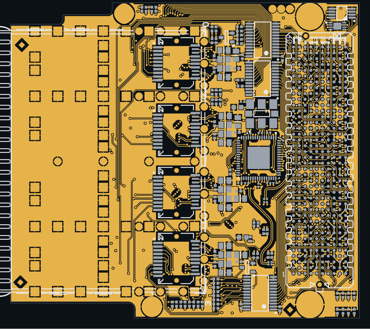
FMC SFP 4CHA (OHWR0039 R1) is an open-hardware circuit board from the CERN Open Hardware Repository, designed in Altium Designer: a 6-layer board of 76.5 × 69 mm with 347 components and 281 nets, published under CERN-OHL-1.1.
review 94% walked · 12 findings: 5 major · 7 minor (154 items)
Open in the interactive viewerRead the full review
Design review
Probe recorded 12 findings: 5 major · 7 minor (154 items) on this design. Each is shown here with its reasoning; the full review links every one to the pins, nets and datasheet pages it rests on.
OSC1 must be a Si571 VCXO, but the BOM names one Si570 part for both oscillators
OSC1 must be a Si571 VCXO, but the published BOM names one Si570 part for both oscillators, so built as listed the AD9510 cannot steer OSC1.
The oscillators
Site Pin 1 on this board Needed part BOM part OSC1 NetC66_2, the AD9510 CP loop-filter node (R64 30k, C66 820 pF) Si571 (pin 1 = control voltage) Si570BBC000121DG, shared row OSC2 unconnected Si570 (XO) Si570BBC000121DG, shared row On a Si570, pin 1 is a no-connect: 'Make no external connection to this pin' (Si570/Si571 datasheet, p.29). Only the Si571 has the control-voltage pin (Table 15, p.30).
``
mermaid flowchart LR CP["AD9510 CP<br/>charge pump"] -- "R64 / C66 loop filter" --> V["OSC1 pin 1<br/>NetC66_2"] V --> O["OSC1<br/>Si570 per BOM"] O -- "CLK2_P / CLK2_N" --> A["AD9510 CLK2"]``Why it matters
Built as listed, the clocks on CLK2 never lock to the FMC reference on REFIN.
- DiffPairMismatchmajorOpen
DiffPairMismatch: 3 nets×3
Checked by the review, stands · Claude walker (cern session) — These FMC LA/HA pairs are used as single-ended signals, so the pin-count asymmetry is real and deliberate, with no matched-pair routing consequence. HA22_P goes to IC2 (AD9510) pin 18 and HA22_N is unused. LA_03_P/N go through 0R R50/R59 to OSC1 pin 2 and OSC2 pin 2 (oscillator OE), with R80 2k2 pull-up on LA_03_N. HA23_P goes through R52 200R to SDO, and HA23_N carries the MCP9801 ALERT (IC23 pin 3) with R102 10k to VADJ. Stands as stated.
At HA22_P, HA23_P, LA_03_P
Each finding, with its own headline
HA22_P'HA22_P' / 'HA22_N' (pair inferred from names) is pin-count asymmetric (2 vs 1)
Differential pair 'HA22_P' / 'HA22_N', INFERRED FROM THE NET NAMES (nothing in the design declares it a pair), is pin-count asymmetric (2 vs 1) - one side reaches a pin the other does not, so the two halves cannot be routed as a matched pair. NOTE: this check does not verify WHICH contact either net reaches; a correctly-symmetric pair can still be swapped at a connector.
HA23_P'HA23_P' / 'HA23_N' (pair inferred from names) is pin-count asymmetric (2 vs 3)
Differential pair 'HA23_P' / 'HA23_N', INFERRED FROM THE NET NAMES (nothing in the design declares it a pair), is pin-count asymmetric (2 vs 3) - one side reaches a pin the other does not, so the two halves cannot be routed as a matched pair. NOTE: this check does not verify WHICH contact either net reaches; a correctly-symmetric pair can still be swapped at a connector.
LA_03_P'LA_03_P' / 'LA_03_N' (pair inferred from names) is pin-count asymmetric (2 vs 3)
Differential pair 'LA_03_P' / 'LA_03_N', INFERRED FROM THE NET NAMES (nothing in the design declares it a pair), is pin-count asymmetric (2 vs 3) - one side reaches a pin the other does not, so the two halves cannot be routed as a matched pair. NOTE: this check does not verify WHICH contact either net reaches; a correctly-symmetric pair can still be swapped at a connector.
- ReferencePlaneDiscontinuitymajorOpen
ReferencePlaneDiscontinuity: 120 boards×120
Checked by the review, stands · Claude walker W3 (Cern session) — Checked: the reference break is read from the copper as stated. Whether it matters depends on the signal's edge rate and the receiver's margin, which no datasheet or app note on file fixes for this net; the impedance step and reflection figures are Probe's model, and the thresholds are its starting values. Layout practice, not a datasheet requirement. Left for the owner.
At along@SIGNAL_LAYER_2:GND|P3V3, along@SIGNAL_LAYER_2:P3V3|VADJ, merged:30.65,53.54|30.7,52.71, merged:36.21,20.87|36.82,21.32, merged:46.18,1.9|46.38,1.11, merged:48.58,30.09|48.8,29.31 and 114 more
Each finding, with its own headline — 100 of 120 shown
along@SIGNAL_LAYER_2:GND|P3V37 nets run ALONG the split between the GND and P3V3 planes on SIGNAL_LAYER_2 at 7 places, the longest 13.16 mm; the impedance rises from 71 ohm to 104 ohm there at worst, 19.1 % of each edge reflected (fastest: SFP3_LOS at 100 ps 10-90 %, ASSUMED)
On SIGNAL_LAYER_2 the GND and P3V3 planes part, and 7 nets run down the slot between them at 7 place(s), rather than across it. This is not a crossing: the return still follows the track, in the plane on its other side and in the slot's edges, so it does not detour. What changes is the track's own impedance. With the plane gone from under it on this side for that length, its field reaches further, to the slot's edges and to the next plane beyond, so its capacitance falls and its impedance rises; every edge travelling down it is partly reflected where it enters the stretch and again where it leaves, by (Z2 - Z1)/(Z2 + Z1). The longer the stretch against the edge's rise, the more of the edge sees the full step. A crossing is generally the worse fault; a mismatch is not free. Over solid plane each track is 71 ohm; along the slot 72 ohm to 104 ohm, reflecting up to 19.1 % of each edge (a method-of-moments field solve of the cross-section, one dielectric; were the slot's edges to carry none of the return, up to 107 ohm). At 1 of the 7 place(s) the rise is within 10 %, the tolerance controlled impedance is commonly built to (the stackup states none); the rest exceed it or cannot be said, so the finding is a warning. One decision covers the split line's slot: whether these tracks may run down it, or should be moved over solid plane.
- 'SFP5_MODDEF0' on TOPLAYER at (40.97, 62.8), 13.22 mm, running ALONG the split for 8.85 mm, not across it, 71 ohm over solid plane, 104 ohm along it: 19.1 % of each edge reflected; other side: none: the signal layer is outermost
- 'SFP6_MODDEF0' on TOPLAYER at (40.8, 63.05), 9.28 mm, running ALONG the split for 5.29 mm, not across it, 71 ohm over solid plane, 103 ohm along it: 18.8 % of each edge reflected; other side: none: the signal layer is outermost
- 'SFP5_TXFAULT' on TOPLAYER at (41.15, 62.55), 19.31 mm, running ALONG the split for 12.7 mm, not across it, 71 ohm over solid plane, 102 ohm along it: 18 % of each edge reflected; other side: none: the signal layer is outermost
- 'SFP4_MODDEF0' on TOPLAYER at (41.21, 62.3), 19.77 mm, running ALONG the split for 13.16 mm, not across it, 71 ohm over solid plane, 92 ohm along it: 13.3 % of each edge reflected; other side: none: the signal layer is outermost
- 'SFP4_TXFAULT' on TOPLAYER at (41.2, 61.57), 3.04 mm, running ALONG the split for 2.42 mm, not across it, 71 ohm over solid plane, 89 ohm along it: 11.3 % of each edge reflected; other side: none: the signal layer is outermost
- 'SFP4_LOS' on TOPLAYER at (30.07, 61.44), 18.71 mm, running ALONG the split for 12.75 mm, not across it, 71 ohm over solid plane, 80 ohm along it: 6.1 % of each edge reflected; other side: none: the signal layer is outermost
- 'SFP3_LOS' on TOPLAYER at (34.16, 1.55), 7.93 mm, running ALONG the split for 2.46 mm, not across it, 71 ohm over solid plane, 72 ohm along it: 0.9 % of each edge reflected; other side: none: the signal layer is outermost
Every site is a row of this finding's evidence, keyed by net, layers and position. GET /api/odb/boards/40/reference-planes?group=along%40SIGNAL_LAYER_2%3AGND%7CP3V3 serves each with its own layer_image region; all of them lie in x 23.12..43.6, y -1.07..64.05 mm (board frame, Y up).
Read from the copper as drawn on the reference layer, along each track's centreline at exact breakpoints. The reference is the copper beside the track, never the layer's type or name. Whether it matters depends on each signal's edge rate, which nothing on file states for these nets: a slow static line crosses a split harmlessly, a fast edge does not.
along@SIGNAL_LAYER_2:P3V3|VADJ6 nets run ALONG the split between the P3V3 and VADJ planes on SIGNAL_LAYER_2 at 6 places, the longest 21.57 mm; the impedance rises from 71 ohm to 94 ohm there at worst, 14.1 % of each edge reflected (fastest: S5_MOD_DEF0 at 100 ps 10-90 %, ASSUMED)
On SIGNAL_LAYER_2 the P3V3 and VADJ planes part, and 6 nets run down the slot between them at 6 place(s), rather than across it. This is not a crossing: the return still follows the track, in the plane on its other side and in the slot's edges, so it does not detour. What changes is the track's own impedance. With the plane gone from under it on this side for that length, its field reaches further, to the slot's edges and to the next plane beyond, so its capacitance falls and its impedance rises; every edge travelling down it is partly reflected where it enters the stretch and again where it leaves, by (Z2 - Z1)/(Z2 + Z1). The longer the stretch against the edge's rise, the more of the edge sees the full step. A crossing is generally the worse fault; a mismatch is not free. Over solid plane each track is 71 ohm; along the slot 73 ohm to 94 ohm, reflecting up to 14.1 % of each edge (a method-of-moments field solve of the cross-section, one dielectric; were the slot's edges to carry none of the return, up to 107 ohm). At 3 of the 6 place(s) the rise is within 10 %, the tolerance controlled impedance is commonly built to (the stackup states none); the rest exceed it or cannot be said, so the finding is a warning. One decision covers the split line's slot: whether these tracks may run down it, or should be moved over solid plane.
- 'S2_TX_DISABLE' on TOPLAYER at (74.33, 8.89), 1.89 mm, running ALONG the split for 1.49 mm, not across it, 71 ohm over solid plane, 94 ohm along it: 14.1 % of each edge reflected; other side: none: the signal layer is outermost
- 'S1_TX_DISABLE' on TOPLAYER at (74.59, 16.04), 17.5 mm, running ALONG the split for 14.54 mm, not across it, 71 ohm over solid plane, 79 ohm along it: 5.4 % of each edge reflected; other side: none: the signal layer is outermost
- 'SFP0_LOS' on TOPLAYER at (56.65, 53.16), 1.08 mm, running ALONG the split for 0.57 mm, not across it, 71 ohm over solid plane, 79 ohm along it: 5.3 % of each edge reflected; other side: none: the signal layer is outermost
- 'S7_TX_DISABLE' on TOPLAYER at (74.43, 42.99), 18.38 mm, running ALONG the split for 15.35 mm, not across it, 71 ohm over solid plane, 77 ohm along it: 4.3 % of each edge reflected; other side: none: the signal layer is outermost
- 'S7_RATE_SEL' on TOPLAYER at (74.71, 44.14), 24.28 mm, running ALONG the split for 21.57 mm, not across it, 71 ohm over solid plane, 75 ohm along it: 2.9 % of each edge reflected; other side: none: the signal layer is outermost
- 'S5_MOD_DEF0' on TOPLAYER at (61.02, 52.6), 1.82 mm, running ALONG the split for 1.3 mm, not across it, 71 ohm over solid plane, 73 ohm along it: 1.9 % of each edge reflected; other side: none: the signal layer is outermost
Every site is a row of this finding's evidence, keyed by net, layers and position. GET /api/odb/boards/40/reference-planes?group=along%40SIGNAL_LAYER_2%3AP3V3%7CVADJ serves each with its own layer_image region; all of them lie in x 55.37..75.71, y 6.94..56.69 mm (board frame, Y up).
Read from the copper as drawn on the reference layer, along each track's centreline at exact breakpoints. The reference is the copper beside the track, never the layer's type or name. Whether it matters depends on each signal's edge rate, which nothing on file states for these nets: a slow static line crosses a split harmlessly, a fast edge does not.
merged:30.65,53.54|30.7,52.71'SFP4_MODDEF0' crosses between the drills at (30.7, 52.71) and (30.65, 53.54), whose anti-pads run together in the GND plane on GND_1 (fastest: SFP4_MODDEF0 at 100 ps 10-90 %, ASSUMED)
Along 'SFP4_MODDEF0' on BOTTOMLAYER, the GND plane on GND_1 is cleared round the drills at (30.7, 52.71) and (30.65, 53.54), and the two clearances run together: the straight line from one drill to the other is bare all the way, and the track crosses it, over 0.62 mm of bare stretch at (30.7, 53.12). Past one drill's anti-pad the return flows round on either side; here it cannot pass between the drills and detours round the whole merged clearance - the slot a row of pins or vias cuts in a plane. No crossing has a plane on the track's other side, so the whole return meets the break.
- 'SFP4_MODDEF0' on BOTTOMLAYER at (30.7, 53.12), 0.62 mm between the drills at (30.7, 52.71) and (30.65, 53.54) in GND_1; other side: none: the signal layer is outermost
Every site is a row of this finding's evidence, keyed by net, layers and position. GET /api/odb/boards/40/reference-planes?group=merged%3A30.65%2C53.54%7C30.7%2C52.71 serves each with its own layer_image region; all of them lie in x 29.37..31.99, y 52.12..54.12 mm (board frame, Y up).
Read from the copper as drawn on the reference layer, along each track's centreline at exact breakpoints. The reference is the copper beside the track, never the layer's type or name. Whether it matters depends on each signal's edge rate, which nothing on file states for these nets: a slow static line crosses a split harmlessly, a fast edge does not.
merged:36.21,20.87|36.82,21.32'NetIC30C_6' crosses between the drills at (36.2, 20.87) and (36.82, 21.32), whose anti-pads run together in GND's negative-plane field (fastest: NetIC30C_6 at 100 ps 10-90 %, ASSUMED)
Along 'NetIC30C_6' on SIGNAL_LAYER_2, GND's negative-plane field is cleared round the drills at (36.2, 20.87) and (36.82, 21.32), and the two clearances run together: the straight line from one drill to the other is bare all the way, and the track crosses it, over 0.76 mm of bare stretch at (36.58, 21.08). Past one drill's anti-pad the return flows round on either side; here it cannot pass between the drills and detours round the whole merged clearance - the slot a row of pins or vias cuts in a plane. No crossing has a plane on the track's other side, so the whole return meets the break.
- 'NetIC30C_6' on SIGNAL_LAYER_2 at (36.58, 21.08), 0.76 mm between the drills at (36.2, 20.87) and (36.82, 21.32) in GND; other side: no plane on TOPLAYER
Every site is a row of this finding's evidence, keyed by net, layers and position. GET /api/odb/boards/40/reference-planes?group=merged%3A36.21%2C20.87%7C36.82%2C21.32 serves each with its own layer_image region; all of them lie in x 35.29..37.83, y 19.82..22.36 mm (board frame, Y up).
Read from the copper as drawn on the reference layer, along each track's centreline at exact breakpoints. The reference is the copper beside the track, never the layer's type or name. Whether it matters depends on each signal's edge rate, which nothing on file states for these nets: a slow static line crosses a split harmlessly, a fast edge does not.
merged:46.18,1.9|46.38,1.11'SFP2_MODDEF0' crosses between the drills at (46.18, 1.9) and (46.38, 1.11), whose anti-pads run together in GND's negative-plane field (fastest: SFP2_MODDEF0 at 100 ps 10-90 %, ASSUMED)
Along 'SFP2_MODDEF0' on SIGNAL_LAYER_2, GND's negative-plane field is cleared round the drills at (46.18, 1.9) and (46.38, 1.11), and the two clearances run together: the straight line from one drill to the other is bare all the way, and the track crosses it, over 0.89 mm of bare stretch at (46.59, 1.6). Past one drill's anti-pad the return flows round on either side; here it cannot pass between the drills and detours round the whole merged clearance - the slot a row of pins or vias cuts in a plane. No crossing has a plane on the track's other side, so the whole return meets the break.
- 'SFP2_MODDEF0' on SIGNAL_LAYER_2 at (46.59, 1.6), 0.89 mm between the drills at (46.18, 1.9) and (46.38, 1.11) in GND; other side: no plane on TOPLAYER
Every site is a row of this finding's evidence, keyed by net, layers and position. GET /api/odb/boards/40/reference-planes?group=merged%3A46.18%2C1.9%7C46.38%2C1.11 serves each with its own layer_image region; all of them lie in x 44.91..47.7, y 0.48..2.71 mm (board frame, Y up).
Read from the copper as drawn on the reference layer, along each track's centreline at exact breakpoints. The reference is the copper beside the track, never the layer's type or name. Whether it matters depends on each signal's edge rate, which nothing on file states for these nets: a slow static line crosses a split harmlessly, a fast edge does not.
merged:48.58,30.09|48.8,29.31'HA18_N' crosses between the drills at (48.8, 29.31) and (48.58, 30.09), whose anti-pads run together in the GND plane on GND_1 (fastest: HA18_N at 100 ps 10-90 %, ASSUMED)
Along 'HA18_N' on BOTTOMLAYER, the GND plane on GND_1 is cleared round the drills at (48.8, 29.31) and (48.58, 30.09), and the two clearances run together: the straight line from one drill to the other is bare all the way, and the track crosses it, over 1.33 mm of bare stretch at (48.08, 29.7). Past one drill's anti-pad the return flows round on either side; here it cannot pass between the drills and detours round the whole merged clearance - the slot a row of pins or vias cuts in a plane. No crossing has a plane on the track's other side, so the whole return meets the break.
- 'HA18_N' on BOTTOMLAYER at (48.08, 29.7), 1.33 mm between the drills at (48.8, 29.31) and (48.58, 30.09) in GND_1; other side: none: the signal layer is outermost
Every site is a row of this finding's evidence, keyed by net, layers and position. GET /api/odb/boards/40/reference-planes?group=merged%3A48.58%2C30.09%7C48.8%2C29.31 serves each with its own layer_image region; all of them lie in x 46.83..50.04, y 28.7..30.9 mm (board frame, Y up).
Read from the copper as drawn on the reference layer, along each track's centreline at exact breakpoints. The reference is the copper beside the track, never the layer's type or name. Whether it matters depends on each signal's edge rate, which nothing on file states for these nets: a slow static line crosses a split harmlessly, a fast edge does not.
merged:59.52,31.47|59.72,29.97'GBT1_P' crosses between the drills at (59.72, 29.97) and (59.51, 31.47), whose anti-pads run together in the GND plane on GND_1 (fastest: GBT1_P at 100 ps 10-90 %, ASSUMED)
Along 'GBT1_P' on BOTTOMLAYER, the GND plane on GND_1 is cleared round the drills at (59.72, 29.97) and (59.51, 31.47), and the two clearances run together: the straight line from one drill to the other is bare all the way, and the track crosses it, over 1.1 mm of bare stretch at (59.41, 30.43). Past one drill's anti-pad the return flows round on either side; here it cannot pass between the drills and detours round the whole merged clearance - the slot a row of pins or vias cuts in a plane. No crossing has a plane on the track's other side, so the whole return meets the break.
- 'GBT1_P' on BOTTOMLAYER at (59.41, 30.43), 1.1 mm between the drills at (59.72, 29.97) and (59.51, 31.47) in GND_1; other side: none: the signal layer is outermost
Every site is a row of this finding's evidence, keyed by net, layers and position. GET /api/odb/boards/40/reference-planes?group=merged%3A59.52%2C31.47%7C59.72%2C29.97 serves each with its own layer_image region; all of them lie in x 58.24..61.2, y 29.43..31.57 mm (board frame, Y up).
Read from the copper as drawn on the reference layer, along each track's centreline at exact breakpoints. The reference is the copper beside the track, never the layer's type or name. Whether it matters depends on each signal's edge rate, which nothing on file states for these nets: a slow static line crosses a split harmlessly, a fast edge does not.
merged:59.72,30.57|59.79,29.05'GBT1_N' crosses between the drills at (59.79, 29.04) and (59.72, 30.57), whose anti-pads run together in the GND plane on GND_1 (fastest: GBT1_N at 100 ps 10-90 %, ASSUMED)
Along 'GBT1_N' on BOTTOMLAYER, the GND plane on GND_1 is cleared round the drills at (59.79, 29.04) and (59.72, 30.57), and the two clearances run together: the straight line from one drill to the other is bare all the way, and the track crosses it, over 1.1 mm of bare stretch at (59.39, 30.1). Past one drill's anti-pad the return flows round on either side; here it cannot pass between the drills and detours round the whole merged clearance - the slot a row of pins or vias cuts in a plane. No crossing has a plane on the track's other side, so the whole return meets the break.
- 'GBT1_N' on BOTTOMLAYER at (59.39, 30.1), 1.1 mm between the drills at (59.79, 29.04) and (59.72, 30.57) in GND_1; other side: none: the signal layer is outermost
Every site is a row of this finding's evidence, keyed by net, layers and position. GET /api/odb/boards/40/reference-planes?group=merged%3A59.72%2C30.57%7C59.79%2C29.05 serves each with its own layer_image region; all of them lie in x 58.24..61.2, y 28.97..31.1 mm (board frame, Y up).
Read from the copper as drawn on the reference layer, along each track's centreline at exact breakpoints. The reference is the copper beside the track, never the layer's type or name. Whether it matters depends on each signal's edge rate, which nothing on file states for these nets: a slow static line crosses a split harmlessly, a fast edge does not.
merged:61.1,34.41|61.34,33.46'HA21_N' crosses between the drills at (61.34, 33.46) and (61.1, 34.41), whose anti-pads run together in the GND plane on GND_1 (fastest: HA21_N at 100 ps 10-90 %, ASSUMED)
Along 'HA21_N' on BOTTOMLAYER, the GND plane on GND_1 is cleared round the drills at (61.34, 33.46) and (61.1, 34.41), and the two clearances run together: the straight line from one drill to the other is bare all the way, and the track crosses it, over 1.23 mm of bare stretch at (60.71, 34.47). Past one drill's anti-pad the return flows round on either side; here it cannot pass between the drills and detours round the whole merged clearance - the slot a row of pins or vias cuts in a plane. No crossing has a plane on the track's other side, so the whole return meets the break.
- 'HA21_N' on BOTTOMLAYER at (60.71, 34.47), 1.23 mm between the drills at (61.34, 33.46) and (61.1, 34.41) in GND_1; other side: none: the signal layer is outermost
Every site is a row of this finding's evidence, keyed by net, layers and position. GET /api/odb/boards/40/reference-planes?group=merged%3A61.1%2C34.41%7C61.34%2C33.46 serves each with its own layer_image region; all of them lie in x 59.7..62.37, y 32.98..35.7 mm (board frame, Y up).
Read from the copper as drawn on the reference layer, along each track's centreline at exact breakpoints. The reference is the copper beside the track, never the layer's type or name. Whether it matters depends on each signal's edge rate, which nothing on file states for these nets: a slow static line crosses a split harmlessly, a fast edge does not.
merged:61.44,29.14|62.34,28.73'HA22_P' crosses between the drills at (61.44, 29.14) and (62.34, 28.73), whose anti-pads run together in the GND plane on GND_1 (fastest: HA22_P at 100 ps 10-90 %, ASSUMED)
Along 'HA22_P' on BOTTOMLAYER, the GND plane on GND_1 is cleared round the drills at (61.44, 29.14) and (62.34, 28.73), and the two clearances run together: the straight line from one drill to the other is bare all the way, and the track crosses it, over 0.63 mm of bare stretch at (61.71, 28.87). Past one drill's anti-pad the return flows round on either side; here it cannot pass between the drills and detours round the whole merged clearance - the slot a row of pins or vias cuts in a plane. No crossing has a plane on the track's other side, so the whole return meets the break.
- 'HA22_P' on BOTTOMLAYER at (61.71, 28.87), 0.63 mm between the drills at (61.44, 29.14) and (62.34, 28.73) in GND_1; other side: none: the signal layer is outermost
Every site is a row of this finding's evidence, keyed by net, layers and position. GET /api/odb/boards/40/reference-planes?group=merged%3A61.44%2C29.14%7C62.34%2C28.73 serves each with its own layer_image region; all of them lie in x 60.49..62.93, y 27.64..30.09 mm (board frame, Y up).
Read from the copper as drawn on the reference layer, along each track's centreline at exact breakpoints. The reference is the copper beside the track, never the layer's type or name. Whether it matters depends on each signal's edge rate, which nothing on file states for these nets: a slow static line crosses a split harmlessly, a fast edge does not.
refchange:GND|VADJ17 nets change reference between GND and VADJ at 20 vias, none with a reference that continues across (fastest: GA0 at 100 ps 10-90 %, ASSUMED)
At 20 via(s), on 17 net(s), the signal leaves a layer referenced by one of GND and VADJ for a layer referenced by the other, and no plane references both layers. Different nets: no via can carry the return across; only decoupling between the two planes near the via can. The capacitor carrying the return across was measured at each via, at the knee of the crossing net's edge against 50 ohm assumed: 20 with none. 20 of them at an ASSUMED edge (no edge on file for the net): state one (net_timing_state) and it is re-read. One decision covers the pair: whether GND and VADJ are decoupled to each other near these vias. A via whose layers have more references than these two is a site of each pair it joins. None is partial: at every one, no reference continues across the via.
- 'GA0' at (69.37, 63.75), TOPLAYER -> BOTTOMLAYER: VADJ on SIGNAL_LAYER_2 to GND on GND_1; pure, no reference continues across; stitching none, 20.4 mm of track past the via on BOTTOMLAYER: At the 5 GHz knee of a 100 ps edge (100 ps 10-90 %, assumed: no edge is on file for the net) no capacitor carries the return; only the planes do. GND and VADJ are not a thin pair (at most 0.2 mm), so their own capacitance does not carry the return. To serve it, change layers across the same plane, or move the signal to a layer referenced to ground. None.
- 'GA0' at (69.42, 60.87), TOPLAYER -> BOTTOMLAYER: VADJ on SIGNAL_LAYER_2 to GND on GND_1; pure, no reference continues across; stitching none, 20.4 mm of track past the via on BOTTOMLAYER: At the 5 GHz knee of a 100 ps edge (100 ps 10-90 %, assumed: no edge is on file for the net) no capacitor carries the return; only the planes do. GND and VADJ are not a thin pair (at most 0.2 mm), so their own capacitance does not carry the return. To serve it, change layers across the same plane, or move the signal to a layer referenced to ground. None.
- 'GA1' at (69.17, 59.8), TOPLAYER -> BOTTOMLAYER: VADJ on SIGNAL_LAYER_2 to GND on GND_1; pure, no reference continues across; stitching none, 18.2 mm of track past the via on BOTTOMLAYER: At the 5 GHz knee of a 100 ps edge (100 ps 10-90 %, assumed: no edge is on file for the net) no capacitor carries the return; only the planes do. GND and VADJ are not a thin pair (at most 0.2 mm), so their own capacitance does not carry the return. To serve it, change layers across the same plane, or move the signal to a layer referenced to ground. None.
- 'GA1' at (69.34, 63.12), TOPLAYER -> BOTTOMLAYER: VADJ on SIGNAL_LAYER_2 to GND on GND_1; pure, no reference continues across; stitching none, 18.2 mm of track past the via on BOTTOMLAYER: At the 5 GHz knee of a 100 ps edge (100 ps 10-90 %, assumed: no edge is on file for the net) no capacitor carries the return; only the planes do. GND and VADJ are not a thin pair (at most 0.2 mm), so their own capacitance does not carry the return. To serve it, change layers across the same plane, or move the signal to a layer referenced to ground. None.
- 'S7_TX_DISABLE' at (72.76, 56.93), TOPLAYER -> BOTTOMLAYER: VADJ on SIGNAL_LAYER_2 to GND on GND_1; pure, no reference continues across; stitching none, 15.1 mm of track past the via on BOTTOMLAYER: At the 5 GHz knee of a 100 ps edge (3 ns 10-90 %, assumed: no edge is on file for the net) no capacitor carries the return; only the planes do. GND and VADJ are not a thin pair (at most 0.2 mm), so their own capacitance does not carry the return. To serve it, change layers across the same plane, or move the signal to a layer referenced to ground. None.
- 'S6_RATE_SEL' at (69.37, 58.01), TOPLAYER -> BOTTOMLAYER: VADJ on SIGNAL_LAYER_2 to GND on GND_1; pure, no reference continues across; stitching none, 13.2 mm of track past the via on BOTTOMLAYER: At the 5 GHz knee of a 100 ps edge (20 ns 10-90 %, assumed: no edge is on file for the net) no capacitor carries the return; only the planes do. GND and VADJ are not a thin pair (at most 0.2 mm), so their own capacitance does not carry the return. To serve it, change layers across the same plane, or move the signal to a layer referenced to ground. None.
- 'S5_TX_DISABLE' at (67.63, 57.86), TOPLAYER -> BOTTOMLAYER: VADJ on SIGNAL_LAYER_2 to GND on GND_1; pure, no reference continues across; stitching none, 10.6 mm of track past the via on BOTTOMLAYER: At the 5 GHz knee of a 100 ps edge (3 ns 10-90 %, assumed: no edge is on file for the net) no capacitor carries the return; only the planes do. GND and VADJ are not a thin pair (at most 0.2 mm), so their own capacitance does not carry the return. To serve it, change layers across the same plane, or move the signal to a layer referenced to ground. None.
- 'S4_RATE_SEL' at (66.66, 57.6), TOPLAYER -> BOTTOMLAYER: VADJ on SIGNAL_LAYER_2 to GND on GND_1; pure, no reference continues across; stitching none, 9.5 mm of track past the via on BOTTOMLAYER: At the 5 GHz knee of a 100 ps edge (20 ns 10-90 %, assumed: no edge is on file for the net) no capacitor carries the return; only the planes do. GND and VADJ are not a thin pair (at most 0.2 mm), so their own capacitance does not carry the return. To serve it, change layers across the same plane, or move the signal to a layer referenced to ground. None.
- 'S4_LED' at (70.86, 4.37), TOPLAYER -> BOTTOMLAYER: VADJ on SIGNAL_LAYER_2 to GND on GND_1; pure, no reference continues across; stitching none, 9.1 mm of track past the via on BOTTOMLAYER: At the 5 GHz knee of a 100 ps edge (100 ps 10-90 %, assumed: no edge is on file for the net) no capacitor carries the return; only the planes do. GND and VADJ are not a thin pair (at most 0.2 mm), so their own capacitance does not carry the return. To serve it, change layers across the same plane, or move the signal to a layer referenced to ground. None.
- 'S5_LED' at (70.27, 3.68), TOPLAYER -> BOTTOMLAYER: VADJ on SIGNAL_LAYER_2 to GND on GND_1; pure, no reference continues across; stitching none, 7.5 mm of track past the via on BOTTOMLAYER: At the 5 GHz knee of a 100 ps edge (100 ps 10-90 %, assumed: no edge is on file for the net) no capacitor carries the return; only the planes do. GND and VADJ are not a thin pair (at most 0.2 mm), so their own capacitance does not carry the return. To serve it, change layers across the same plane, or move the signal to a layer referenced to ground. None.
- 'HA23_N' at (73.86, 63.78), TOPLAYER -> BOTTOMLAYER: VADJ on SIGNAL_LAYER_2 to GND on GND_1; pure, no reference continues across; stitching none, 6.7 mm of track past the via on BOTTOMLAYER: At the 5 GHz knee of a 100 ps edge (100 ps 10-90 %, assumed: no edge is on file for the net) no capacitor carries the return; only the planes do. GND and VADJ are not a thin pair (at most 0.2 mm), so their own capacitance does not carry the return. To serve it, change layers across the same plane, or move the signal to a layer referenced to ground. None.
- 'HA23_N' at (75.34, 58.76), TOPLAYER -> BOTTOMLAYER: VADJ on SIGNAL_LAYER_2 to GND on GND_1; pure, no reference continues across; stitching none, 6.7 mm of track past the via on BOTTOMLAYER: At the 5 GHz knee of a 100 ps edge (100 ps 10-90 %, assumed: no edge is on file for the net) no capacitor carries the return; only the planes do. GND and VADJ are not a thin pair (at most 0.2 mm), so their own capacitance does not carry the return. To serve it, change layers across the same plane, or move the signal to a layer referenced to ground. None.
- and 8 more
Every site is a row of this finding's evidence, keyed by net, layers and position. GET /api/odb/boards/40/reference-planes?group=refchange%3AGND%7CVADJ serves each with its own layer_image region; all of them lie in x 58.31..77.34, y -0.8..65.78 mm (board frame, Y up).
The reference on each layer is the first plane the track meets leaving the via, anti-pads and the net's own copper skipped. Whether it matters depends on each signal's edge rate, which nothing on file states for these nets: a slow static line crosses a split harmlessly, a fast edge does not.
split@SIGNAL_LAYER_2:GND|P3V38 nets cross the split between the GND and P3V3 planes on SIGNAL_LAYER_2 at 8 places, with no plane on the track's other side (fastest: NetIC30C_5 at 100 ps 10-90 %, ASSUMED)
On SIGNAL_LAYER_2 the GND and P3V3 planes part, and 8 nets cross from one to the other at 8 place(s). The return current cannot follow a track across; it detours to wherever the two planes are joined (a stitching capacitor, or the source), and the loop it opens radiates and couples. One decision covers the boundary: whether it is stitched near these crossings, or the nets crossing it are slow enough not to care. Tracks that run ALONG this split, down the slot rather than across it, are a finding of their own: theirs is an impedance step, not a detour. At 0 of the 8 crossing(s) the track's other neighbour carries a plane, which the return can use there; 8 are on an outer layer, with no other neighbour. No crossing has a plane on the track's other side, so the whole return meets the break.
- 'NetIC30C_5' on TOPLAYER at (45.21, 17.07), 0.58 mm; other side: none: the signal layer is outermost
- 'NetIC30C_6' on TOPLAYER at (45.21, 17.64), 0.58 mm; other side: none: the signal layer is outermost
- 'NetJ5A_3' on TOPLAYER at (45.21, 14.77), 0.58 mm; other side: none: the signal layer is outermost
- 'NetJ5B_3' on TOPLAYER at (45.21, 14.52), 0.58 mm; other side: none: the signal layer is outermost
- 'NetJ5G_3' on TOPLAYER at (42.4, 60.94), 0.4 mm; other side: none: the signal layer is outermost
- 'NetJ5H_3' on TOPLAYER at (42.39, 60.69), 0.41 mm; other side: none: the signal layer is outermost
- 'SFP4_RS0' on TOPLAYER at (45.3, 44.5), 0.58 mm; other side: none: the signal layer is outermost
- 'SFP6_RS0' on TOPLAYER at (45.21, 46.51), 0.58 mm; other side: none: the signal layer is outermost
Every site is a row of this finding's evidence, keyed by net, layers and position. GET /api/odb/boards/40/reference-planes?group=split%40SIGNAL_LAYER_2%3AGND%7CP3V3 serves each with its own layer_image region; all of them lie in x 41.2..46.5, y 13.52..61.94 mm (board frame, Y up).
Read from the copper as drawn on the reference layer, along each track's centreline at exact breakpoints. The reference is the copper beside the track, never the layer's type or name. Whether it matters depends on each signal's edge rate, which nothing on file states for these nets: a slow static line crosses a split harmlessly, a fast edge does not.
split@SIGNAL_LAYER_2:P3V3|VADJ41 nets cross the split between the P3V3 and VADJ planes on SIGNAL_LAYER_2 at 50 places, with no plane on the track's other side (fastest: S0_LOS at 100 ps 10-90 %, ASSUMED)
On SIGNAL_LAYER_2 the P3V3 and VADJ planes part, and 41 nets cross from one to the other at 50 place(s). The return current cannot follow a track across; it detours to wherever the two planes are joined (a stitching capacitor, or the source), and the loop it opens radiates and couples. One decision covers the boundary: whether it is stitched near these crossings, or the nets crossing it are slow enough not to care. Tracks that run ALONG this split, down the slot rather than across it, are a finding of their own: theirs is an impedance step, not a detour. At 0 of the 50 crossing(s) the track's other neighbour carries a plane, which the return can use there; 50 are on an outer layer, with no other neighbour. No crossing has a plane on the track's other side, so the whole return meets the break.
- 'S0_LOS' on TOPLAYER at (59.06, 47.47), 0.23 mm; other side: none: the signal layer is outermost
- 'S0_MOD_DEF0' on TOPLAYER at (59.06, 48.12), 0.23 mm; other side: none: the signal layer is outermost
- 'S0_RATE_SEL' on TOPLAYER at (74.3, 24.62), 1.87 mm; other side: none: the signal layer is outermost
- 'S0_TX_DISABLE' on TOPLAYER at (74.13, 27.33), 1.62 mm; other side: none: the signal layer is outermost
- 'S0_TX_FAULT' on TOPLAYER at (59.1, 48.7), 0.29 mm; other side: none: the signal layer is outermost
- 'S1_LOS' on TOPLAYER at (58.66, 6.22), 0.34 mm; other side: none: the signal layer is outermost
- 'S1_MOD_DEF0' on TOPLAYER at (58.91, 6.22), 0.34 mm; other side: none: the signal layer is outermost
- 'S1_TX_FAULT' on TOPLAYER at (59.1, 46.74), 0.29 mm; other side: none: the signal layer is outermost
- 'S2_LOS' on TOPLAYER at (59.44, 6.22), 0.34 mm; other side: none: the signal layer is outermost
- 'S2_MOD_DEF0' on TOPLAYER at (59.69, 6.22), 0.34 mm; other side: none: the signal layer is outermost
- 'S2_RATE_SEL' on TOPLAYER at (65.34, 6.21), 0.36 mm; other side: none: the signal layer is outermost
- 'S2_TX_FAULT' on TOPLAYER at (59.19, 6.22), 0.34 mm; other side: none: the signal layer is outermost
- and 38 more
Every site is a row of this finding's evidence, keyed by net, layers and position. GET /api/odb/boards/40/reference-planes?group=split%40SIGNAL_LAYER_2%3AP3V3%7CVADJ serves each with its own layer_image region; all of them lie in x 55.37..75.71, y 5.01..60.86 mm (board frame, Y up).
Read from the copper as drawn on the reference layer, along each track's centreline at exact breakpoints. The reference is the copper beside the track, never the layer's type or name. Whether it matters depends on each signal's edge rate, which nothing on file states for these nets: a slow static line crosses a split harmlessly, a fast edge does not.
split@TOPLAYER:GND|P3V32 nets cross the split between the GND and P3V3 planes on TOPLAYER at 3 places, all with a plane on the track's other side (fastest: NetIC30A_5 at 100 ps 10-90 %, ASSUMED)
On TOPLAYER the GND and P3V3 planes part, and 2 nets cross from one to the other at 3 place(s). The return current cannot follow a track across; it detours to wherever the two planes are joined (a stitching capacitor, or the source), and the loop it opens radiates and couples. One decision covers the boundary: whether it is stitched near these crossings, or the nets crossing it are slow enough not to care. Tracks that run ALONG this split, down the slot rather than across it, are a finding of their own: theirs is an impedance step, not a detour. At 3 of the 3 crossing(s) the track's other neighbour carries a plane, which the return can use there. 0 of the 3 crossing(s) have a plane on the track's other side at most twice as far away as the broken one (to first order each plane beside a stripline carries a share of the return inversely proportional to its distance from the track). The rest leave most or all of the return to the break, so the finding is a warning.
- 'NetIC30A_5' on SIGNAL_LAYER_2 at (48.13, 21.89), 1.33 mm; other side: (negative-layer field) on GND, 0.46 mm from the track against 0.18 mm to TOPLAYER: 72% of the return on TOPLAYER
- 'NetIC30A_5' on SIGNAL_LAYER_2 at (49.95, 22.52), 0.29 mm; other side: (negative-layer field) on GND, 0.46 mm from the track against 0.18 mm to TOPLAYER: 72% of the return on TOPLAYER
- 'NetIC30A_6' on SIGNAL_LAYER_2 at (49.95, 22.73), 0.29 mm; other side: (negative-layer field) on GND, 0.46 mm from the track against 0.18 mm to TOPLAYER: 72% of the return on TOPLAYER
Every site is a row of this finding's evidence, keyed by net, layers and position. GET /api/odb/boards/40/reference-planes?group=split%40TOPLAYER%3AGND%7CP3V3 serves each with its own layer_image region; all of them lie in x 46.9..51.16, y 19.97..23.73 mm (board frame, Y up).
Read from the copper as drawn on the reference layer, along each track's centreline at exact breakpoints. The reference is the copper beside the track, never the layer's type or name. Whether it matters depends on each signal's edge rate, which nothing on file states for these nets: a slow static line crosses a split harmlessly, a fast edge does not.
void:GND@GND_1:hole 26.59,-3.81|77.01,-2.79'NetIC30D_5' crosses one void in the GND plane on GND_1 at 1 place, the longest 8.17 mm (fastest: NetIC30D_5 at 100 ps 10-90 %, ASSUMED)
Along 'NetIC30D_5' on BOTTOMLAYER, the GND plane on GND_1 has 8.17 mm under the track with no copper, at (48.44, -2.92), the same plane on both sides. No single drill's anti-pad and no landing explains it: a clearance is excused only when it holds a drill and is drawn round it, or the track ends in it on the net's own pad or via, or runs through its own via's clearance and no farther. The return current detours round the void. 1 of them run ALONG the bare copper, parallel to its edges, rather than across it (the longest 7.81 mm). What cleared it: the hole at x 26.59..77.01, y -3.81..-2.79. One decision covers the void: whether these tracks may cross it, or the plane should be filled under them. No crossing has a plane on the track's other side, so the whole return meets the break.
- 'NetIC30D_5' on BOTTOMLAYER at (48.44, -2.92), 8.17 mm, running ALONG the bare copper for 7.81 mm, not across it over no copper; other side: none: the signal layer is outermost
Every site is a row of this finding's evidence, keyed by net, layers and position. GET /api/odb/boards/40/reference-planes?group=void%3AGND%40GND_1%3Ahole%2026.59%2C-3.81%7C77.01%2C-2.79 serves each with its own layer_image region; all of them lie in x 43.4..53.47, y -3.92..-1.79 mm (board frame, Y up).
Read from the copper as drawn on the reference layer, along each track's centreline at exact breakpoints. The reference is the copper beside the track, never the layer's type or name. Whether it matters depends on each signal's edge rate, which nothing on file states for these nets: a slow static line crosses a split harmlessly, a fast edge does not.
void:GND@GND_1:hole 75.99,-3.81|77.01,66.21'S0_LED' crosses one void in the GND plane on GND_1 at 1 place, the longest 31.45 mm (fastest: S0_LED at 100 ps 10-90 %, ASSUMED)
Along 'S0_LED' on BOTTOMLAYER, the GND plane on GND_1 has 31.45 mm under the track with no copper, at (76.1, 19.61), the same plane on both sides. No single drill's anti-pad and no landing explains it: a clearance is excused only when it holds a drill and is drawn round it, or the track ends in it on the net's own pad or via, or runs through its own via's clearance and no farther. The return current detours round the void. 1 of them run ALONG the bare copper, parallel to its edges, rather than across it (the longest 31.15 mm). What cleared it: the hole at x 75.99..77.01, y -3.81..66.21. One decision covers the void: whether these tracks may cross it, or the plane should be filled under them. No crossing has a plane on the track's other side, so the whole return meets the break.
- 'S0_LED' on BOTTOMLAYER at (76.1, 19.61), 31.45 mm, running ALONG the bare copper for 31.15 mm, not across it over no copper; other side: none: the signal layer is outermost
Every site is a row of this finding's evidence, keyed by net, layers and position. GET /api/odb/boards/40/reference-planes?group=void%3AGND%40GND_1%3Ahole%2075.99%2C-3.81%7C77.01%2C66.21 serves each with its own layer_image region; all of them lie in x 74.99..77.1, y 2.93..36.29 mm (board frame, Y up).
Read from the copper as drawn on the reference layer, along each track's centreline at exact breakpoints. The reference is the copper beside the track, never the layer's type or name. Whether it matters depends on each signal's edge rate, which nothing on file states for these nets: a slow static line crosses a split harmlessly, a fast edge does not.
void:GND@SIGNAL_LAYER_2:34.61,9.95'NetIC30D_5' crosses where the outline of the GND plane on SIGNAL_LAYER_2 is drawn back, at 1 place, the longest 0.37 mm (fastest: NetIC30D_5 at 100 ps 10-90 %, ASSUMED)
Along 'NetIC30D_5' on TOPLAYER, the GND plane on SIGNAL_LAYER_2 has 0.37 mm under the track with no copper, at (34.61, 9.95), the same plane on both sides. No single drill's anti-pad and no landing explains it: a clearance is excused only when it holds a drill and is drawn round it, or the track ends in it on the net's own pad or via, or runs through its own via's clearance and no farther. The return current detours round the void. 1 of them run ALONG the bare copper, parallel to its edges, rather than across it (the longest 0.36 mm). No hole cleared it: the outline of the pour at x 0.13..76.15, y -3.13..62.78 is drawn back there. One decision covers the void: whether these tracks may cross it, or the plane should be filled under them. No crossing has a plane on the track's other side, so the whole return meets the break.
- 'NetIC30D_5' on TOPLAYER at (34.61, 9.95), 0.37 mm, running ALONG the bare copper for 0.36 mm, not across it over no copper; other side: none: the signal layer is outermost
Every site is a row of this finding's evidence, keyed by net, layers and position. GET /api/odb/boards/40/reference-planes?group=void%3AGND%40SIGNAL_LAYER_2%3A34.61%2C9.95 serves each with its own layer_image region; all of them lie in x 33.61..35.61, y 8.77..11.14 mm (board frame, Y up).
Read from the copper as drawn on the reference layer, along each track's centreline at exact breakpoints. The reference is the copper beside the track, never the layer's type or name. Whether it matters depends on each signal's edge rate, which nothing on file states for these nets: a slow static line crosses a split harmlessly, a fast edge does not.
void:GND@SIGNAL_LAYER_2:hole 28.77,19.3|30.97,39.87 nets cross one void in the GND plane on SIGNAL_LAYER_2 and the GND plane on TOPLAYER at 6 places, the longest 0.54 mm; 12 over tracks of other nets routed inside it (fastest: NetJ5B_3 at 100 ps 10-90 %, ASSUMED)
Along 'NetJ5B_3' on SIGNAL_LAYER_2, the GND plane on TOPLAYER has 0.54 mm under the track with copper of SFP_RS1C, not a plane, at (30.12, 20.89), the same plane on both sides. No single drill's anti-pad and no landing explains it: a clearance is excused only when it holds a drill and is drawn round it, or the track ends in it on the net's own pad or via, or runs through its own via's clearance and no farther. The return current detours round the void. 12 of the crossings pass over tracks of other nets routed inside the hole on the reference layer: the plane is absent there, and those tracks stand in it. 6 places on 7 net(s) cross it, listed below, the longest first. What cleared it: the hole at x 28.77..30.97, y 19.3..39.8. One decision covers the void: whether these tracks may cross it, or the plane should be filled under them. 0 of the 12 crossing(s) have a plane on the track's other side at most twice as far away as the broken one (to first order each plane beside a stripline carries a share of the return inversely proportional to its distance from the track). The rest leave most or all of the return to the break, so the finding is a warning.
- one crossing of two tracks, seen from each: 'NetJ5B_3' on SIGNAL_LAYER_2 at (30.12, 20.89), 0.54 mm over copper of SFP_RS1C, not a plane; other side: (negative-layer field) on GND, 0.46 mm from the track against 0.18 mm to TOPLAYER: 72% of the return on TOPLAYER / 'SFP_RS1C' on TOPLAYER at (30.12, 21.07), 0.42 mm over copper of NetJ5B_3, not a plane; other side: none: the signal layer is outermost
- one crossing of two tracks, seen from each: 'NetJ5B_3' on SIGNAL_LAYER_2 at (29.48, 34.92), 0.38 mm over copper of SFP_RS1B, not a plane; other side: (negative-layer field) on GND, 0.46 mm from the track against 0.18 mm to TOPLAYER: 72% of the return on TOPLAYER / 'SFP_RS1B' on TOPLAYER at (29.48, 34.79), 0.31 mm over copper of NetJ5B_3, not a plane; other side: none: the signal layer is outermost
- one crossing of two tracks, seen from each: 'NetJ5B_3' on SIGNAL_LAYER_2 at (29.48, 36.25), 0.38 mm over copper of NetJ5B_7, not a plane; other side: (negative-layer field) on GND, 0.46 mm from the track against 0.18 mm to TOPLAYER: 72% of the return on TOPLAYER / 'NetJ5B_7' on TOPLAYER at (29.48, 36.38), 0.31 mm over copper of NetJ5B_3, not a plane; other side: none: the signal layer is outermost
- one crossing of two tracks, seen from each: 'NetJ5B_3' on SIGNAL_LAYER_2 at (30.12, 21.87), 0.38 mm over copper of SFP2_LOS, not a plane; other side: (negative-layer field) on GND, 0.46 mm from the track against 0.18 mm to TOPLAYER: 72% of the return on TOPLAYER / 'SFP2_LOS' on TOPLAYER at (30.12, 21.99), 0.31 mm over copper of NetJ5B_3, not a plane; other side: none: the signal layer is outermost
- one crossing of two tracks, seen from each: 'NetJ5B_3' on SIGNAL_LAYER_2 at (30.12, 22.73), 0.38 mm over copper of NetJ5C_7, not a plane; other side: (negative-layer field) on GND, 0.46 mm from the track against 0.18 mm to TOPLAYER: 72% of the return on TOPLAYER / 'NetJ5C_7' on TOPLAYER at (30.12, 22.86), 0.31 mm over copper of NetJ5B_3, not a plane; other side: none: the signal layer is outermost
- one crossing of two tracks, seen from each: 'NetJ5B_3' on SIGNAL_LAYER_2 at (30.12, 23.55), 0.38 mm over copper of SFP2_MODDEF0, not a plane; other side: (negative-layer field) on GND, 0.46 mm from the track against 0.18 mm to TOPLAYER: 72% of the return on TOPLAYER / 'SFP2_MODDEF0' on TOPLAYER at (30.12, 23.68), 0.31 mm over copper of NetJ5B_3, not a plane; other side: none: the signal layer is outermost
Every site is a row of this finding's evidence, keyed by net, layers and position. GET /api/odb/boards/40/reference-planes?group=void%3AGND%40SIGNAL_LAYER_2%3Ahole%2028.77%2C19.3%7C30.97%2C39.8 serves each with its own layer_image region; all of them lie in x 28.32..31.27, y 19.8..37.57 mm (board frame, Y up).
Read from the copper as drawn on the reference layer, along each track's centreline at exact breakpoints. The reference is the copper beside the track, never the layer's type or name. Whether it matters depends on each signal's edge rate, which nothing on file states for these nets: a slow static line crosses a split harmlessly, a fast edge does not.
void:GND@SIGNAL_LAYER_2:hole 39.11,59.55|40.31,60.75'NetJ5H_3' crosses one void in the GND plane on SIGNAL_LAYER_2 at 1 place, the longest 1.2 mm (fastest: NetJ5H_3 at 100 ps 10-90 %, ASSUMED)
Along 'NetJ5H_3' on TOPLAYER, the GND plane on SIGNAL_LAYER_2 has 1.2 mm under the track with no copper, at (39.71, 60.69), the same plane on both sides. No single drill's anti-pad and no landing explains it: a clearance is excused only when it holds a drill and is drawn round it, or the track ends in it on the net's own pad or via, or runs through its own via's clearance and no farther. The return current detours round the void. 1 of them run ALONG the bare copper, parallel to its edges, rather than across it (the longest 1.2 mm). What cleared it: the hole at x 39.11..40.31, y 59.55..60.75. One decision covers the void: whether these tracks may cross it, or the plane should be filled under them. No crossing has a plane on the track's other side, so the whole return meets the break.
- 'NetJ5H_3' on TOPLAYER at (39.71, 60.69), 1.2 mm, running ALONG the bare copper for 1.2 mm, not across it over no copper; other side: none: the signal layer is outermost
Every site is a row of this finding's evidence, keyed by net, layers and position. GET /api/odb/boards/40/reference-planes?group=void%3AGND%40SIGNAL_LAYER_2%3Ahole%2039.11%2C59.55%7C40.31%2C60.75 serves each with its own layer_image region; all of them lie in x 38.11..41.31, y 59.69..61.69 mm (board frame, Y up).
Read from the copper as drawn on the reference layer, along each track's centreline at exact breakpoints. The reference is the copper beside the track, never the layer's type or name. Whether it matters depends on each signal's edge rate, which nothing on file states for these nets: a slow static line crosses a split harmlessly, a fast edge does not.
void:GND@SIGNAL_LAYER_2:hole 40.42,59.55|41.62,60.75'NetJ5H_3' crosses one void in the GND plane on SIGNAL_LAYER_2 at 1 place, the longest 1.2 mm (fastest: NetJ5H_3 at 100 ps 10-90 %, ASSUMED)
Along 'NetJ5H_3' on TOPLAYER, the GND plane on SIGNAL_LAYER_2 has 1.2 mm under the track with no copper, at (41.02, 60.69), the same plane on both sides. No single drill's anti-pad and no landing explains it: a clearance is excused only when it holds a drill and is drawn round it, or the track ends in it on the net's own pad or via, or runs through its own via's clearance and no farther. The return current detours round the void. 1 of them run ALONG the bare copper, parallel to its edges, rather than across it (the longest 1.2 mm). What cleared it: the hole at x 40.42..41.62, y 59.55..60.75. One decision covers the void: whether these tracks may cross it, or the plane should be filled under them. No crossing has a plane on the track's other side, so the whole return meets the break.
- 'NetJ5H_3' on TOPLAYER at (41.02, 60.69), 1.2 mm, running ALONG the bare copper for 1.2 mm, not across it over no copper; other side: none: the signal layer is outermost
Every site is a row of this finding's evidence, keyed by net, layers and position. GET /api/odb/boards/40/reference-planes?group=void%3AGND%40SIGNAL_LAYER_2%3Ahole%2040.42%2C59.55%7C41.62%2C60.75 serves each with its own layer_image region; all of them lie in x 39.42..42.62, y 59.69..61.69 mm (board frame, Y up).
Read from the copper as drawn on the reference layer, along each track's centreline at exact breakpoints. The reference is the copper beside the track, never the layer's type or name. Whether it matters depends on each signal's edge rate, which nothing on file states for these nets: a slow static line crosses a split harmlessly, a fast edge does not.
void:GND@TOPLAYER:24.22,45.25'NetIC30A_6' crosses where the outline of the GND plane on TOPLAYER is drawn back, at 1 place, the longest 2.51 mm (fastest: NetIC30A_6 at 100 ps 10-90 %, ASSUMED)
Along 'NetIC30A_6' on SIGNAL_LAYER_2, the GND plane on TOPLAYER has 2.51 mm under the track with no copper, at (24.22, 45.25), the same plane on both sides. No single drill's anti-pad and no landing explains it: a clearance is excused only when it holds a drill and is drawn round it, or the track ends in it on the net's own pad or via, or runs through its own via's clearance and no farther. The return current detours round the void. 1 of them run ALONG the bare copper, parallel to its edges, rather than across it (the longest 2.51 mm). No hole cleared it: the outline of the pour at x 0.13..76.16, y -3.13..65.63 is drawn back there. One decision covers the void: whether these tracks may cross it, or the plane should be filled under them. 0 of the 1 crossing(s) have a plane on the track's other side at most twice as far away as the broken one (to first order each plane beside a stripline carries a share of the return inversely proportional to its distance from the track). The rest leave most or all of the return to the break, so the finding is a warning.
- 'NetIC30A_6' on SIGNAL_LAYER_2 at (24.22, 45.25), 2.51 mm, running ALONG the bare copper for 2.51 mm, not across it over no copper; other side: (negative-layer field) on GND, 0.46 mm from the track against 0.18 mm to TOPLAYER: 72% of the return on TOPLAYER
Every site is a row of this finding's evidence, keyed by net, layers and position. GET /api/odb/boards/40/reference-planes?group=void%3AGND%40TOPLAYER%3A24.22%2C45.25 serves each with its own layer_image region; all of them lie in x 23.22..25.22, y 43..47.5 mm (board frame, Y up).
Read from the copper as drawn on the reference layer, along each track's centreline at exact breakpoints. The reference is the copper beside the track, never the layer's type or name. Whether it matters depends on each signal's edge rate, which nothing on file states for these nets: a slow static line crosses a split harmlessly, a fast edge does not.
void:GND@TOPLAYER:26.8,17.75'SFP2_MODDEF0' crosses where the outline of the GND plane on TOPLAYER is drawn back, at 1 place, the longest 6.5 mm (fastest: SFP2_MODDEF0 at 100 ps 10-90 %, ASSUMED)
Along 'SFP2_MODDEF0' on SIGNAL_LAYER_2, the GND plane on TOPLAYER has 6.5 mm under the track with no copper, at (26.8, 17.75), the same plane on both sides. No single drill's anti-pad and no landing explains it: a clearance is excused only when it holds a drill and is drawn round it, or the track ends in it on the net's own pad or via, or runs through its own via's clearance and no farther. The return current detours round the void. 1 of them run ALONG the bare copper, parallel to its edges, rather than across it (the longest 6.5 mm). No hole cleared it: the outline of the pour at x 0.13..76.16, y -3.13..65.63 is drawn back there. One decision covers the void: whether these tracks may cross it, or the plane should be filled under them. 0 of the 1 crossing(s) have a plane on the track's other side at most twice as far away as the broken one (to first order each plane beside a stripline carries a share of the return inversely proportional to its distance from the track). The rest leave most or all of the return to the break, so the finding is a warning.
- 'SFP2_MODDEF0' on SIGNAL_LAYER_2 at (26.8, 17.75), 6.5 mm, running ALONG the bare copper for 6.5 mm, not across it over no copper; other side: (negative-layer field) on GND, 0.46 mm from the track against 0.18 mm to TOPLAYER: 72% of the return on TOPLAYER
Every site is a row of this finding's evidence, keyed by net, layers and position. GET /api/odb/boards/40/reference-planes?group=void%3AGND%40TOPLAYER%3A26.8%2C17.75 serves each with its own layer_image region; all of them lie in x 25.8..27.8, y 13.5..22.01 mm (board frame, Y up).
Read from the copper as drawn on the reference layer, along each track's centreline at exact breakpoints. The reference is the copper beside the track, never the layer's type or name. Whether it matters depends on each signal's edge rate, which nothing on file states for these nets: a slow static line crosses a split harmlessly, a fast edge does not.
void:GND@TOPLAYER:27.31,63'SFP_RS1B' crosses where the outline of the GND plane on TOPLAYER is drawn back, at 1 place, the longest 0.54 mm (fastest: SFP_RS1B at 100 ps 10-90 %, ASSUMED)
Along 'SFP_RS1B' on SIGNAL_LAYER_2, the GND plane on TOPLAYER has 0.54 mm under the track with no copper, at (27.31, 63), the same plane on both sides. No single drill's anti-pad and no landing explains it: a clearance is excused only when it holds a drill and is drawn round it, or the track ends in it on the net's own pad or via, or runs through its own via's clearance and no farther. The return current detours round the void. No hole cleared it: the outline of the pour at x 0.13..76.16, y -3.13..65.63 is drawn back there. One decision covers the void: whether these tracks may cross it, or the plane should be filled under them. 0 of the 1 crossing(s) have a plane on the track's other side at most twice as far away as the broken one (to first order each plane beside a stripline carries a share of the return inversely proportional to its distance from the track). The rest leave most or all of the return to the break, so the finding is a warning.
- 'SFP_RS1B' on SIGNAL_LAYER_2 at (27.31, 63), 0.54 mm over no copper; other side: (negative-layer field) on GND, 0.46 mm from the track against 0.18 mm to TOPLAYER: 72% of the return on TOPLAYER
Every site is a row of this finding's evidence, keyed by net, layers and position. GET /api/odb/boards/40/reference-planes?group=void%3AGND%40TOPLAYER%3A27.31%2C63 serves each with its own layer_image region; all of them lie in x 26.31..28.31, y 61.73..64.27 mm (board frame, Y up).
Read from the copper as drawn on the reference layer, along each track's centreline at exact breakpoints. The reference is the copper beside the track, never the layer's type or name. Whether it matters depends on each signal's edge rate, which nothing on file states for these nets: a slow static line crosses a split harmlessly, a fast edge does not.
void:GND@TOPLAYER:27.31,63.64'SFP_RS1B' crosses where the outline of the GND plane on TOPLAYER is drawn back, at 1 place, the longest 0.54 mm (fastest: SFP_RS1B at 100 ps 10-90 %, ASSUMED)
Along 'SFP_RS1B' on SIGNAL_LAYER_2, the GND plane on TOPLAYER has 0.54 mm under the track with no copper, at (27.31, 63.64), the same plane on both sides. No single drill's anti-pad and no landing explains it: a clearance is excused only when it holds a drill and is drawn round it, or the track ends in it on the net's own pad or via, or runs through its own via's clearance and no farther. The return current detours round the void. No hole cleared it: the outline of the pour at x 0.13..76.16, y -3.13..65.63 is drawn back there. One decision covers the void: whether these tracks may cross it, or the plane should be filled under them. 0 of the 1 crossing(s) have a plane on the track's other side at most twice as far away as the broken one (to first order each plane beside a stripline carries a share of the return inversely proportional to its distance from the track). The rest leave most or all of the return to the break, so the finding is a warning.
- 'SFP_RS1B' on SIGNAL_LAYER_2 at (27.31, 63.64), 0.54 mm over no copper; other side: (negative-layer field) on GND, 0.46 mm from the track against 0.18 mm to TOPLAYER: 72% of the return on TOPLAYER
Every site is a row of this finding's evidence, keyed by net, layers and position. GET /api/odb/boards/40/reference-planes?group=void%3AGND%40TOPLAYER%3A27.31%2C63.64 serves each with its own layer_image region; all of them lie in x 26.31..28.31, y 62.37..64.91 mm (board frame, Y up).
Read from the copper as drawn on the reference layer, along each track's centreline at exact breakpoints. The reference is the copper beside the track, never the layer's type or name. Whether it matters depends on each signal's edge rate, which nothing on file states for these nets: a slow static line crosses a split harmlessly, a fast edge does not.
void:GND@TOPLAYER:29.15,16.68'NetJ5H_7' crosses where the outline of the GND plane on TOPLAYER is drawn back, at 1 place, the longest 2.41 mm (fastest: NetJ5H_7 at 100 ps 10-90 %, ASSUMED)
Along 'NetJ5H_7' on SIGNAL_LAYER_2, the GND plane on TOPLAYER has 2.41 mm under the track with no copper, at (29.15, 16.68), the same plane on both sides. No single drill's anti-pad and no landing explains it: a clearance is excused only when it holds a drill and is drawn round it, or the track ends in it on the net's own pad or via, or runs through its own via's clearance and no farther. The return current detours round the void. 1 of them run ALONG the bare copper, parallel to its edges, rather than across it (the longest 2.36 mm). No hole cleared it: the outline of the pour at x 0.13..76.16, y -3.13..65.63 is drawn back there. One decision covers the void: whether these tracks may cross it, or the plane should be filled under them. 0 of the 1 crossing(s) have a plane on the track's other side at most twice as far away as the broken one (to first order each plane beside a stripline carries a share of the return inversely proportional to its distance from the track). The rest leave most or all of the return to the break, so the finding is a warning.
- 'NetJ5H_7' on SIGNAL_LAYER_2 at (29.15, 16.68), 2.41 mm, running ALONG the bare copper for 2.36 mm, not across it over no copper; other side: (negative-layer field) on GND, 0.46 mm from the track against 0.18 mm to TOPLAYER: 72% of the return on TOPLAYER
Every site is a row of this finding's evidence, keyed by net, layers and position. GET /api/odb/boards/40/reference-planes?group=void%3AGND%40TOPLAYER%3A29.15%2C16.68 serves each with its own layer_image region; all of them lie in x 28.11..30.15, y 14.5..18.89 mm (board frame, Y up).
Read from the copper as drawn on the reference layer, along each track's centreline at exact breakpoints. The reference is the copper beside the track, never the layer's type or name. Whether it matters depends on each signal's edge rate, which nothing on file states for these nets: a slow static line crosses a split harmlessly, a fast edge does not.
void:GND@TOPLAYER:31.19,55.82'SFP0_MODDEF0' crosses where the outline of the GND plane on TOPLAYER is drawn back, at 1 place, the longest 0.25 mm (fastest: SFP0_MODDEF0 at 100 ps 10-90 %, ASSUMED)
Along 'SFP0_MODDEF0' on SIGNAL_LAYER_2, the GND plane on TOPLAYER has 0.25 mm under the track with no copper, at (31.19, 55.82), the same plane on both sides. No single drill's anti-pad and no landing explains it: a clearance is excused only when it holds a drill and is drawn round it, or the track ends in it on the net's own pad or via, or runs through its own via's clearance and no farther. The return current detours round the void. No hole cleared it: the outline of the pour at x 0.13..76.16, y -3.13..65.63 is drawn back there. One decision covers the void: whether these tracks may cross it, or the plane should be filled under them. 0 of the 1 crossing(s) have a plane on the track's other side at most twice as far away as the broken one (to first order each plane beside a stripline carries a share of the return inversely proportional to its distance from the track). The rest leave most or all of the return to the break, so the finding is a warning.
- 'SFP0_MODDEF0' on SIGNAL_LAYER_2 at (31.19, 55.82), 0.25 mm over no copper; other side: (negative-layer field) on GND, 0.46 mm from the track against 0.18 mm to TOPLAYER: 72% of the return on TOPLAYER
Every site is a row of this finding's evidence, keyed by net, layers and position. GET /api/odb/boards/40/reference-planes?group=void%3AGND%40TOPLAYER%3A31.19%2C55.82 serves each with its own layer_image region; all of them lie in x 30.06..32.31, y 54.82..56.82 mm (board frame, Y up).
Read from the copper as drawn on the reference layer, along each track's centreline at exact breakpoints. The reference is the copper beside the track, never the layer's type or name. Whether it matters depends on each signal's edge rate, which nothing on file states for these nets: a slow static line crosses a split harmlessly, a fast edge does not.
void:GND@TOPLAYER:31.26,56.36'SFP1_TXFAULT' crosses where the outline of the GND plane on TOPLAYER is drawn back, at 1 place, the longest 0.56 mm (fastest: SFP1_TXFAULT at 100 ps 10-90 %, ASSUMED)
Along 'SFP1_TXFAULT' on SIGNAL_LAYER_2, the GND plane on TOPLAYER has 0.56 mm under the track with no copper, at (31.26, 56.36), the same plane on both sides. No single drill's anti-pad and no landing explains it: a clearance is excused only when it holds a drill and is drawn round it, or the track ends in it on the net's own pad or via, or runs through its own via's clearance and no farther. The return current detours round the void. 1 of them run ALONG the bare copper, parallel to its edges, rather than across it (the longest 0.41 mm). No hole cleared it: the outline of the pour at x 0.13..76.16, y -3.13..65.63 is drawn back there. One decision covers the void: whether these tracks may cross it, or the plane should be filled under them. 0 of the 1 crossing(s) have a plane on the track's other side at most twice as far away as the broken one (to first order each plane beside a stripline carries a share of the return inversely proportional to its distance from the track). The rest leave most or all of the return to the break, so the finding is a warning.
- 'SFP1_TXFAULT' on SIGNAL_LAYER_2 at (31.26, 56.36), 0.56 mm, running ALONG the bare copper for 0.41 mm, not across it over no copper; other side: (negative-layer field) on GND, 0.46 mm from the track against 0.18 mm to TOPLAYER: 72% of the return on TOPLAYER
Every site is a row of this finding's evidence, keyed by net, layers and position. GET /api/odb/boards/40/reference-planes?group=void%3AGND%40TOPLAYER%3A31.26%2C56.36 serves each with its own layer_image region; all of them lie in x 30.06..32.58, y 55.36..57.47 mm (board frame, Y up).
Read from the copper as drawn on the reference layer, along each track's centreline at exact breakpoints. The reference is the copper beside the track, never the layer's type or name. Whether it matters depends on each signal's edge rate, which nothing on file states for these nets: a slow static line crosses a split harmlessly, a fast edge does not.
void:GND@TOPLAYER:31.51,13.54'SFP2_TXFAULT' crosses where the outline of the GND plane on TOPLAYER is drawn back, at 1 place, the longest 0.25 mm (fastest: SFP2_TXFAULT at 100 ps 10-90 %, ASSUMED)
Along 'SFP2_TXFAULT' on SIGNAL_LAYER_2, the GND plane on TOPLAYER has 0.25 mm under the track with no copper, at (31.51, 13.54), the same plane on both sides. No single drill's anti-pad and no landing explains it: a clearance is excused only when it holds a drill and is drawn round it, or the track ends in it on the net's own pad or via, or runs through its own via's clearance and no farther. The return current detours round the void. No hole cleared it: the outline of the pour at x 0.13..76.16, y -3.13..65.63 is drawn back there. One decision covers the void: whether these tracks may cross it, or the plane should be filled under them. 0 of the 1 crossing(s) have a plane on the track's other side at most twice as far away as the broken one (to first order each plane beside a stripline carries a share of the return inversely proportional to its distance from the track). The rest leave most or all of the return to the break, so the finding is a warning.
- 'SFP2_TXFAULT' on SIGNAL_LAYER_2 at (31.51, 13.54), 0.25 mm over no copper; other side: (negative-layer field) on GND, 0.46 mm from the track against 0.18 mm to TOPLAYER: 72% of the return on TOPLAYER
Every site is a row of this finding's evidence, keyed by net, layers and position. GET /api/odb/boards/40/reference-planes?group=void%3AGND%40TOPLAYER%3A31.51%2C13.54 serves each with its own layer_image region; all of them lie in x 30.51..32.51, y 12.41..14.67 mm (board frame, Y up).
Read from the copper as drawn on the reference layer, along each track's centreline at exact breakpoints. The reference is the copper beside the track, never the layer's type or name. Whether it matters depends on each signal's edge rate, which nothing on file states for these nets: a slow static line crosses a split harmlessly, a fast edge does not.
void:GND@TOPLAYER:31.51,20.02'SFP2_TXFAULT' crosses where the outline of the GND plane on TOPLAYER is drawn back, at 1 place, the longest 0.25 mm (fastest: SFP2_TXFAULT at 100 ps 10-90 %, ASSUMED)
Along 'SFP2_TXFAULT' on SIGNAL_LAYER_2, the GND plane on TOPLAYER has 0.25 mm under the track with no copper, at (31.51, 20.02), the same plane on both sides. No single drill's anti-pad and no landing explains it: a clearance is excused only when it holds a drill and is drawn round it, or the track ends in it on the net's own pad or via, or runs through its own via's clearance and no farther. The return current detours round the void. No hole cleared it: the outline of the pour at x 0.13..76.16, y -3.13..65.63 is drawn back there. One decision covers the void: whether these tracks may cross it, or the plane should be filled under them. 0 of the 1 crossing(s) have a plane on the track's other side at most twice as far away as the broken one (to first order each plane beside a stripline carries a share of the return inversely proportional to its distance from the track). The rest leave most or all of the return to the break, so the finding is a warning.
- 'SFP2_TXFAULT' on SIGNAL_LAYER_2 at (31.51, 20.02), 0.25 mm over no copper; other side: (negative-layer field) on GND, 0.46 mm from the track against 0.18 mm to TOPLAYER: 72% of the return on TOPLAYER
Every site is a row of this finding's evidence, keyed by net, layers and position. GET /api/odb/boards/40/reference-planes?group=void%3AGND%40TOPLAYER%3A31.51%2C20.02 serves each with its own layer_image region; all of them lie in x 30.51..32.51, y 18.89..21.14 mm (board frame, Y up).
Read from the copper as drawn on the reference layer, along each track's centreline at exact breakpoints. The reference is the copper beside the track, never the layer's type or name. Whether it matters depends on each signal's edge rate, which nothing on file states for these nets: a slow static line crosses a split harmlessly, a fast edge does not.
void:GND@TOPLAYER:31.51,3.05'SFP_RS1H' crosses where the outline of the GND plane on TOPLAYER is drawn back, at 1 place, the longest 2.14 mm (fastest: SFP_RS1H at 100 ps 10-90 %, ASSUMED)
Along 'SFP_RS1H' on SIGNAL_LAYER_2, the GND plane on TOPLAYER has 2.14 mm under the track with no copper, at (31.51, 3.05), the same plane on both sides. No single drill's anti-pad and no landing explains it: a clearance is excused only when it holds a drill and is drawn round it, or the track ends in it on the net's own pad or via, or runs through its own via's clearance and no farther. The return current detours round the void. 1 of them run ALONG the bare copper, parallel to its edges, rather than across it (the longest 1.85 mm). No hole cleared it: the outline of the pour at x 0.13..76.16, y -3.13..65.63 is drawn back there. One decision covers the void: whether these tracks may cross it, or the plane should be filled under them. 0 of the 1 crossing(s) have a plane on the track's other side at most twice as far away as the broken one (to first order each plane beside a stripline carries a share of the return inversely proportional to its distance from the track). The rest leave most or all of the return to the break, so the finding is a warning.
- 'SFP_RS1H' on SIGNAL_LAYER_2 at (31.51, 3.05), 2.14 mm, running ALONG the bare copper for 1.85 mm, not across it over no copper; other side: (negative-layer field) on GND, 0.46 mm from the track against 0.18 mm to TOPLAYER: 72% of the return on TOPLAYER
Every site is a row of this finding's evidence, keyed by net, layers and position. GET /api/odb/boards/40/reference-planes?group=void%3AGND%40TOPLAYER%3A31.51%2C3.05 serves each with its own layer_image region; all of them lie in x 29.42..32.51, y 1.55..4.64 mm (board frame, Y up).
Read from the copper as drawn on the reference layer, along each track's centreline at exact breakpoints. The reference is the copper beside the track, never the layer's type or name. Whether it matters depends on each signal's edge rate, which nothing on file states for these nets: a slow static line crosses a split harmlessly, a fast edge does not.
void:GND@TOPLAYER:31.54,55.57'SFP0_TXFAULT' crosses where the outline of the GND plane on TOPLAYER is drawn back, at 1 place, the longest 1.13 mm (fastest: SFP0_TXFAULT at 100 ps 10-90 %, ASSUMED)
Along 'SFP0_TXFAULT' on SIGNAL_LAYER_2, the GND plane on TOPLAYER has 1.13 mm under the track with copper of GND, not a plane, at (31.54, 55.57), running to the end of the track. No single drill's anti-pad and no landing explains it: a clearance is excused only when it holds a drill and is drawn round it, or the track ends in it on the net's own pad or via, or runs through its own via's clearance and no farther. The return current detours round the void. 1 of them run ALONG the bare copper, parallel to its edges, rather than across it (the longest 0.29 mm). No hole cleared it: the outline of the pour at x 0.13..76.16, y -3.13..65.63 is drawn back there. One decision covers the void: whether these tracks may cross it, or the plane should be filled under them. 0 of the 1 crossing(s) have a plane on the track's other side at most twice as far away as the broken one (to first order each plane beside a stripline carries a share of the return inversely proportional to its distance from the track). The rest leave most or all of the return to the break, so the finding is a warning.
- 'SFP0_TXFAULT' on SIGNAL_LAYER_2 at (31.54, 55.57), 1.13 mm, running ALONG the bare copper for 0.29 mm, not across it over copper of GND, not a plane, to the end of the track; other side: (negative-layer field) on GND, 0.46 mm from the track against 0.18 mm to TOPLAYER: 72% of the return on TOPLAYER
Every site is a row of this finding's evidence, keyed by net, layers and position. GET /api/odb/boards/40/reference-planes?group=void%3AGND%40TOPLAYER%3A31.54%2C55.57 serves each with its own layer_image region; all of them lie in x 29.73..32.89, y 54.24..56.92 mm (board frame, Y up).
Read from the copper as drawn on the reference layer, along each track's centreline at exact breakpoints. The reference is the copper beside the track, never the layer's type or name. Whether it matters depends on each signal's edge rate, which nothing on file states for these nets: a slow static line crosses a split harmlessly, a fast edge does not.
void:GND@TOPLAYER:31.71,13.54'SFP1_MODDEF0' crosses where the outline of the GND plane on TOPLAYER is drawn back, at 1 place, the longest 0.25 mm (fastest: SFP1_MODDEF0 at 100 ps 10-90 %, ASSUMED)
Along 'SFP1_MODDEF0' on SIGNAL_LAYER_2, the GND plane on TOPLAYER has 0.25 mm under the track with no copper, at (31.71, 13.54), the same plane on both sides. No single drill's anti-pad and no landing explains it: a clearance is excused only when it holds a drill and is drawn round it, or the track ends in it on the net's own pad or via, or runs through its own via's clearance and no farther. The return current detours round the void. No hole cleared it: the outline of the pour at x 0.13..76.16, y -3.13..65.63 is drawn back there. One decision covers the void: whether these tracks may cross it, or the plane should be filled under them. 0 of the 1 crossing(s) have a plane on the track's other side at most twice as far away as the broken one (to first order each plane beside a stripline carries a share of the return inversely proportional to its distance from the track). The rest leave most or all of the return to the break, so the finding is a warning.
- 'SFP1_MODDEF0' on SIGNAL_LAYER_2 at (31.71, 13.54), 0.25 mm over no copper; other side: (negative-layer field) on GND, 0.46 mm from the track against 0.18 mm to TOPLAYER: 72% of the return on TOPLAYER
Every site is a row of this finding's evidence, keyed by net, layers and position. GET /api/odb/boards/40/reference-planes?group=void%3AGND%40TOPLAYER%3A31.71%2C13.54 serves each with its own layer_image region; all of them lie in x 30.71..32.71, y 12.41..14.67 mm (board frame, Y up).
Read from the copper as drawn on the reference layer, along each track's centreline at exact breakpoints. The reference is the copper beside the track, never the layer's type or name. Whether it matters depends on each signal's edge rate, which nothing on file states for these nets: a slow static line crosses a split harmlessly, a fast edge does not.
void:GND@TOPLAYER:31.71,20.02'SFP1_MODDEF0' crosses where the outline of the GND plane on TOPLAYER is drawn back, at 1 place, the longest 0.25 mm (fastest: SFP1_MODDEF0 at 100 ps 10-90 %, ASSUMED)
Along 'SFP1_MODDEF0' on SIGNAL_LAYER_2, the GND plane on TOPLAYER has 0.25 mm under the track with no copper, at (31.71, 20.02), the same plane on both sides. No single drill's anti-pad and no landing explains it: a clearance is excused only when it holds a drill and is drawn round it, or the track ends in it on the net's own pad or via, or runs through its own via's clearance and no farther. The return current detours round the void. No hole cleared it: the outline of the pour at x 0.13..76.16, y -3.13..65.63 is drawn back there. One decision covers the void: whether these tracks may cross it, or the plane should be filled under them. 0 of the 1 crossing(s) have a plane on the track's other side at most twice as far away as the broken one (to first order each plane beside a stripline carries a share of the return inversely proportional to its distance from the track). The rest leave most or all of the return to the break, so the finding is a warning.
- 'SFP1_MODDEF0' on SIGNAL_LAYER_2 at (31.71, 20.02), 0.25 mm over no copper; other side: (negative-layer field) on GND, 0.46 mm from the track against 0.18 mm to TOPLAYER: 72% of the return on TOPLAYER
Every site is a row of this finding's evidence, keyed by net, layers and position. GET /api/odb/boards/40/reference-planes?group=void%3AGND%40TOPLAYER%3A31.71%2C20.02 serves each with its own layer_image region; all of them lie in x 30.71..32.71, y 18.89..21.14 mm (board frame, Y up).
Read from the copper as drawn on the reference layer, along each track's centreline at exact breakpoints. The reference is the copper beside the track, never the layer's type or name. Whether it matters depends on each signal's edge rate, which nothing on file states for these nets: a slow static line crosses a split harmlessly, a fast edge does not.
void:GND@TOPLAYER:31.81,45.38'SFP7_MODDEF0' crosses where the outline of the GND plane on TOPLAYER is drawn back, at 1 place, the longest 0.16 mm (fastest: SFP7_MODDEF0 at 100 ps 10-90 %, ASSUMED)
Along 'SFP7_MODDEF0' on SIGNAL_LAYER_2, the GND plane on TOPLAYER has 0.16 mm under the track with no copper, at (31.81, 45.38), the same plane on both sides. No single drill's anti-pad and no landing explains it: a clearance is excused only when it holds a drill and is drawn round it, or the track ends in it on the net's own pad or via, or runs through its own via's clearance and no farther. The return current detours round the void. No hole cleared it: the outline of the pour at x 0.13..76.16, y -3.13..65.63 is drawn back there. One decision covers the void: whether these tracks may cross it, or the plane should be filled under them. 0 of the 1 crossing(s) have a plane on the track's other side at most twice as far away as the broken one (to first order each plane beside a stripline carries a share of the return inversely proportional to its distance from the track). The rest leave most or all of the return to the break, so the finding is a warning.
- 'SFP7_MODDEF0' on SIGNAL_LAYER_2 at (31.81, 45.38), 0.16 mm over no copper; other side: (negative-layer field) on GND, 0.46 mm from the track against 0.18 mm to TOPLAYER: 72% of the return on TOPLAYER
Every site is a row of this finding's evidence, keyed by net, layers and position. GET /api/odb/boards/40/reference-planes?group=void%3AGND%40TOPLAYER%3A31.81%2C45.38 serves each with its own layer_image region; all of them lie in x 30.81..32.81, y 44.3..46.46 mm (board frame, Y up).
Read from the copper as drawn on the reference layer, along each track's centreline at exact breakpoints. The reference is the copper beside the track, never the layer's type or name. Whether it matters depends on each signal's edge rate, which nothing on file states for these nets: a slow static line crosses a split harmlessly, a fast edge does not.
void:GND@TOPLAYER:32.75,57.64'SFP1_TXFAULT' crosses where the outline of the GND plane on TOPLAYER is drawn back, at 1 place, the longest 2.41 mm (fastest: SFP1_TXFAULT at 100 ps 10-90 %, ASSUMED)
Along 'SFP1_TXFAULT' on SIGNAL_LAYER_2, the GND plane on TOPLAYER has 2.41 mm under the track with no copper, at (32.75, 57.64), the same plane on both sides. No single drill's anti-pad and no landing explains it: a clearance is excused only when it holds a drill and is drawn round it, or the track ends in it on the net's own pad or via, or runs through its own via's clearance and no farther. The return current detours round the void. No hole cleared it: the outline of the pour at x 0.13..76.16, y -3.13..65.63 is drawn back there. One decision covers the void: whether these tracks may cross it, or the plane should be filled under them. 0 of the 1 crossing(s) have a plane on the track's other side at most twice as far away as the broken one (to first order each plane beside a stripline carries a share of the return inversely proportional to its distance from the track). The rest leave most or all of the return to the break, so the finding is a warning.
- 'SFP1_TXFAULT' on SIGNAL_LAYER_2 at (32.75, 57.64), 2.41 mm over no copper; other side: (negative-layer field) on GND, 0.46 mm from the track against 0.18 mm to TOPLAYER: 72% of the return on TOPLAYER
Every site is a row of this finding's evidence, keyed by net, layers and position. GET /api/odb/boards/40/reference-planes?group=void%3AGND%40TOPLAYER%3A32.75%2C57.64 serves each with its own layer_image region; all of them lie in x 30.89..34.6, y 55.79..59.49 mm (board frame, Y up).
Read from the copper as drawn on the reference layer, along each track's centreline at exact breakpoints. The reference is the copper beside the track, never the layer's type or name. Whether it matters depends on each signal's edge rate, which nothing on file states for these nets: a slow static line crosses a split harmlessly, a fast edge does not.
void:GND@TOPLAYER:33.04,57.36'SFP0_MODDEF0' crosses where the outline of the GND plane on TOPLAYER is drawn back, at 1 place, the longest 3.22 mm (fastest: SFP0_MODDEF0 at 100 ps 10-90 %, ASSUMED)
Along 'SFP0_MODDEF0' on SIGNAL_LAYER_2, the GND plane on TOPLAYER has 3.22 mm under the track with no copper, at (33.04, 57.36), the same plane on both sides. No single drill's anti-pad and no landing explains it: a clearance is excused only when it holds a drill and is drawn round it, or the track ends in it on the net's own pad or via, or runs through its own via's clearance and no farther. The return current detours round the void. No hole cleared it: the outline of the pour at x 0.13..76.16, y -3.13..65.63 is drawn back there. One decision covers the void: whether these tracks may cross it, or the plane should be filled under them. 0 of the 1 crossing(s) have a plane on the track's other side at most twice as far away as the broken one (to first order each plane beside a stripline carries a share of the return inversely proportional to its distance from the track). The rest leave most or all of the return to the break, so the finding is a warning.
- 'SFP0_MODDEF0' on SIGNAL_LAYER_2 at (33.04, 57.36), 3.22 mm over no copper; other side: (negative-layer field) on GND, 0.46 mm from the track against 0.18 mm to TOPLAYER: 72% of the return on TOPLAYER
Every site is a row of this finding's evidence, keyed by net, layers and position. GET /api/odb/boards/40/reference-planes?group=void%3AGND%40TOPLAYER%3A33.04%2C57.36 serves each with its own layer_image region; all of them lie in x 30.9..35.18, y 55.22..59.49 mm (board frame, Y up).
Read from the copper as drawn on the reference layer, along each track's centreline at exact breakpoints. The reference is the copper beside the track, never the layer's type or name. Whether it matters depends on each signal's edge rate, which nothing on file states for these nets: a slow static line crosses a split harmlessly, a fast edge does not.
void:GND@TOPLAYER:33.23,14.48'SFP1_LOS' crosses where the outline of the GND plane on TOPLAYER is drawn back, at 1 place, the longest 3.16 mm (fastest: SFP1_LOS at 100 ps 10-90 %, ASSUMED)
Along 'SFP1_LOS' on SIGNAL_LAYER_2, the GND plane on TOPLAYER has 3.16 mm under the track with no copper, at (33.23, 14.48), the same plane on both sides. No single drill's anti-pad and no landing explains it: a clearance is excused only when it holds a drill and is drawn round it, or the track ends in it on the net's own pad or via, or runs through its own via's clearance and no farther. The return current detours round the void. No hole cleared it: the outline of the pour at x 0.13..76.16, y -3.13..65.63 is drawn back there. One decision covers the void: whether these tracks may cross it, or the plane should be filled under them. 0 of the 1 crossing(s) have a plane on the track's other side at most twice as far away as the broken one (to first order each plane beside a stripline carries a share of the return inversely proportional to its distance from the track). The rest leave most or all of the return to the break, so the finding is a warning.
- 'SFP1_LOS' on SIGNAL_LAYER_2 at (33.23, 14.48), 3.16 mm over no copper; other side: (negative-layer field) on GND, 0.46 mm from the track against 0.18 mm to TOPLAYER: 72% of the return on TOPLAYER
Every site is a row of this finding's evidence, keyed by net, layers and position. GET /api/odb/boards/40/reference-planes?group=void%3AGND%40TOPLAYER%3A33.23%2C14.48 serves each with its own layer_image region; all of them lie in x 31.16..35.3, y 12.41..16.69 mm (board frame, Y up).
Read from the copper as drawn on the reference layer, along each track's centreline at exact breakpoints. The reference is the copper beside the track, never the layer's type or name. Whether it matters depends on each signal's edge rate, which nothing on file states for these nets: a slow static line crosses a split harmlessly, a fast edge does not.
void:GND@TOPLAYER:33.33,57.36'SFP0_TXFAULT' crosses where the outline of the GND plane on TOPLAYER is drawn back, at 1 place, the longest 3.22 mm (fastest: SFP0_TXFAULT at 100 ps 10-90 %, ASSUMED)
Along 'SFP0_TXFAULT' on SIGNAL_LAYER_2, the GND plane on TOPLAYER has 3.22 mm under the track with no copper, at (33.33, 57.36), the same plane on both sides. No single drill's anti-pad and no landing explains it: a clearance is excused only when it holds a drill and is drawn round it, or the track ends in it on the net's own pad or via, or runs through its own via's clearance and no farther. The return current detours round the void. No hole cleared it: the outline of the pour at x 0.13..76.16, y -3.13..65.63 is drawn back there. One decision covers the void: whether these tracks may cross it, or the plane should be filled under them. 0 of the 1 crossing(s) have a plane on the track's other side at most twice as far away as the broken one (to first order each plane beside a stripline carries a share of the return inversely proportional to its distance from the track). The rest leave most or all of the return to the break, so the finding is a warning.
- 'SFP0_TXFAULT' on SIGNAL_LAYER_2 at (33.33, 57.36), 3.22 mm over no copper; other side: (negative-layer field) on GND, 0.46 mm from the track against 0.18 mm to TOPLAYER: 72% of the return on TOPLAYER
Every site is a row of this finding's evidence, keyed by net, layers and position. GET /api/odb/boards/40/reference-planes?group=void%3AGND%40TOPLAYER%3A33.33%2C57.36 serves each with its own layer_image region; all of them lie in x 31.19..35.47, y 55.22..59.49 mm (board frame, Y up).
Read from the copper as drawn on the reference layer, along each track's centreline at exact breakpoints. The reference is the copper beside the track, never the layer's type or name. Whether it matters depends on each signal's edge rate, which nothing on file states for these nets: a slow static line crosses a split harmlessly, a fast edge does not.
void:GND@TOPLAYER:33.58,57.03'SFP7_TXFAULT' crosses where the outline of the GND plane on TOPLAYER is drawn back, at 1 place, the longest 3.22 mm (fastest: SFP7_TXFAULT at 100 ps 10-90 %, ASSUMED)
Along 'SFP7_TXFAULT' on SIGNAL_LAYER_2, the GND plane on TOPLAYER has 3.22 mm under the track with no copper, at (33.58, 57.03), the same plane on both sides. No single drill's anti-pad and no landing explains it: a clearance is excused only when it holds a drill and is drawn round it, or the track ends in it on the net's own pad or via, or runs through its own via's clearance and no farther. The return current detours round the void. No hole cleared it: the outline of the pour at x 0.13..76.16, y -3.13..65.63 is drawn back there. One decision covers the void: whether these tracks may cross it, or the plane should be filled under them. 0 of the 1 crossing(s) have a plane on the track's other side at most twice as far away as the broken one (to first order each plane beside a stripline carries a share of the return inversely proportional to its distance from the track). The rest leave most or all of the return to the break, so the finding is a warning.
- 'SFP7_TXFAULT' on SIGNAL_LAYER_2 at (33.58, 57.03), 3.22 mm over no copper; other side: (negative-layer field) on GND, 0.46 mm from the track against 0.18 mm to TOPLAYER: 72% of the return on TOPLAYER
Every site is a row of this finding's evidence, keyed by net, layers and position. GET /api/odb/boards/40/reference-planes?group=void%3AGND%40TOPLAYER%3A33.58%2C57.03 serves each with its own layer_image region; all of them lie in x 31.77..36.05, y 55.22..59.49 mm (board frame, Y up).
Read from the copper as drawn on the reference layer, along each track's centreline at exact breakpoints. The reference is the copper beside the track, never the layer's type or name. Whether it matters depends on each signal's edge rate, which nothing on file states for these nets: a slow static line crosses a split harmlessly, a fast edge does not.
void:GND@TOPLAYER:33.62,57.36'SFP7_LOS' crosses where the outline of the GND plane on TOPLAYER is drawn back, at 1 place, the longest 3.22 mm (fastest: SFP7_LOS at 100 ps 10-90 %, ASSUMED)
Along 'SFP7_LOS' on SIGNAL_LAYER_2, the GND plane on TOPLAYER has 3.22 mm under the track with no copper, at (33.62, 57.36), the same plane on both sides. No single drill's anti-pad and no landing explains it: a clearance is excused only when it holds a drill and is drawn round it, or the track ends in it on the net's own pad or via, or runs through its own via's clearance and no farther. The return current detours round the void. No hole cleared it: the outline of the pour at x 0.13..76.16, y -3.13..65.63 is drawn back there. One decision covers the void: whether these tracks may cross it, or the plane should be filled under them. 0 of the 1 crossing(s) have a plane on the track's other side at most twice as far away as the broken one (to first order each plane beside a stripline carries a share of the return inversely proportional to its distance from the track). The rest leave most or all of the return to the break, so the finding is a warning.
- 'SFP7_LOS' on SIGNAL_LAYER_2 at (33.62, 57.36), 3.22 mm over no copper; other side: (negative-layer field) on GND, 0.46 mm from the track against 0.18 mm to TOPLAYER: 72% of the return on TOPLAYER
Every site is a row of this finding's evidence, keyed by net, layers and position. GET /api/odb/boards/40/reference-planes?group=void%3AGND%40TOPLAYER%3A33.62%2C57.36 serves each with its own layer_image region; all of them lie in x 31.48..35.76, y 55.22..59.49 mm (board frame, Y up).
Read from the copper as drawn on the reference layer, along each track's centreline at exact breakpoints. The reference is the copper beside the track, never the layer's type or name. Whether it matters depends on each signal's edge rate, which nothing on file states for these nets: a slow static line crosses a split harmlessly, a fast edge does not.
void:GND@TOPLAYER:33.69,14.28'NetJ5C_3' crosses where the outline of the GND plane on TOPLAYER is drawn back, at 1 place, the longest 3 mm (fastest: NetJ5C_3 at 100 ps 10-90 %, ASSUMED)
Along 'NetJ5C_3' on SIGNAL_LAYER_2, the GND plane on TOPLAYER has 3 mm under the track with no copper, at (33.69, 14.28), the same plane on both sides. No single drill's anti-pad and no landing explains it: a clearance is excused only when it holds a drill and is drawn round it, or the track ends in it on the net's own pad or via, or runs through its own via's clearance and no farther. The return current detours round the void. No hole cleared it: the outline of the pour at x 0.13..76.16, y -3.13..65.63 is drawn back there. One decision covers the void: whether these tracks may cross it, or the plane should be filled under them. 0 of the 1 crossing(s) have a plane on the track's other side at most twice as far away as the broken one (to first order each plane beside a stripline carries a share of the return inversely proportional to its distance from the track). The rest leave most or all of the return to the break, so the finding is a warning.
- 'NetJ5C_3' on SIGNAL_LAYER_2 at (33.69, 14.28), 3 mm over no copper; other side: (negative-layer field) on GND, 0.46 mm from the track against 0.18 mm to TOPLAYER: 72% of the return on TOPLAYER
Every site is a row of this finding's evidence, keyed by net, layers and position. GET /api/odb/boards/40/reference-planes?group=void%3AGND%40TOPLAYER%3A33.69%2C14.28 serves each with its own layer_image region; all of them lie in x 31.82..35.56, y 12.41..16.69 mm (board frame, Y up).
Read from the copper as drawn on the reference layer, along each track's centreline at exact breakpoints. The reference is the copper beside the track, never the layer's type or name. Whether it matters depends on each signal's edge rate, which nothing on file states for these nets: a slow static line crosses a split harmlessly, a fast edge does not.
void:GND@TOPLAYER:34.2,57.36'SFP6_LOS' crosses where the outline of the GND plane on TOPLAYER is drawn back, at 1 place, the longest 3.22 mm (fastest: SFP6_LOS at 100 ps 10-90 %, ASSUMED)
Along 'SFP6_LOS' on SIGNAL_LAYER_2, the GND plane on TOPLAYER has 3.22 mm under the track with no copper, at (34.2, 57.36), the same plane on both sides. No single drill's anti-pad and no landing explains it: a clearance is excused only when it holds a drill and is drawn round it, or the track ends in it on the net's own pad or via, or runs through its own via's clearance and no farther. The return current detours round the void. No hole cleared it: the outline of the pour at x 0.13..76.16, y -3.13..65.63 is drawn back there. One decision covers the void: whether these tracks may cross it, or the plane should be filled under them. 0 of the 1 crossing(s) have a plane on the track's other side at most twice as far away as the broken one (to first order each plane beside a stripline carries a share of the return inversely proportional to its distance from the track). The rest leave most or all of the return to the break, so the finding is a warning.
- 'SFP6_LOS' on SIGNAL_LAYER_2 at (34.2, 57.36), 3.22 mm over no copper; other side: (negative-layer field) on GND, 0.46 mm from the track against 0.18 mm to TOPLAYER: 72% of the return on TOPLAYER
Every site is a row of this finding's evidence, keyed by net, layers and position. GET /api/odb/boards/40/reference-planes?group=void%3AGND%40TOPLAYER%3A34.2%2C57.36 serves each with its own layer_image region; all of them lie in x 32.06..36.34, y 55.22..59.49 mm (board frame, Y up).
Read from the copper as drawn on the reference layer, along each track's centreline at exact breakpoints. The reference is the copper beside the track, never the layer's type or name. Whether it matters depends on each signal's edge rate, which nothing on file states for these nets: a slow static line crosses a split harmlessly, a fast edge does not.
void:GND@TOPLAYER:34.3,19.39'SFP1_LOS' crosses where the outline of the GND plane on TOPLAYER is drawn back, at 1 place, the longest 2.26 mm (fastest: SFP1_LOS at 100 ps 10-90 %, ASSUMED)
Along 'SFP1_LOS' on SIGNAL_LAYER_2, the GND plane on TOPLAYER has 2.26 mm under the track with no copper, at (34.3, 19.39), the same plane on both sides. No single drill's anti-pad and no landing explains it: a clearance is excused only when it holds a drill and is drawn round it, or the track ends in it on the net's own pad or via, or runs through its own via's clearance and no farther. The return current detours round the void. No hole cleared it: the outline of the pour at x 0.13..76.16, y -3.13..65.63 is drawn back there. One decision covers the void: whether these tracks may cross it, or the plane should be filled under them. 0 of the 1 crossing(s) have a plane on the track's other side at most twice as far away as the broken one (to first order each plane beside a stripline carries a share of the return inversely proportional to its distance from the track). The rest leave most or all of the return to the break, so the finding is a warning.
- 'SFP1_LOS' on SIGNAL_LAYER_2 at (34.3, 19.39), 2.26 mm over no copper; other side: (negative-layer field) on GND, 0.46 mm from the track against 0.18 mm to TOPLAYER: 72% of the return on TOPLAYER
Every site is a row of this finding's evidence, keyed by net, layers and position. GET /api/odb/boards/40/reference-planes?group=void%3AGND%40TOPLAYER%3A34.3%2C19.39 serves each with its own layer_image region; all of them lie in x 33.3..35.3, y 17.26..21.52 mm (board frame, Y up).
Read from the copper as drawn on the reference layer, along each track's centreline at exact breakpoints. The reference is the copper beside the track, never the layer's type or name. Whether it matters depends on each signal's edge rate, which nothing on file states for these nets: a slow static line crosses a split harmlessly, a fast edge does not.
void:GND@TOPLAYER:34.47,57.34'SFP7_MODDEF0' crosses where the outline of the GND plane on TOPLAYER is drawn back, at 1 place, the longest 3.27 mm (fastest: SFP7_MODDEF0 at 100 ps 10-90 %, ASSUMED)
Along 'SFP7_MODDEF0' on SIGNAL_LAYER_2, the GND plane on TOPLAYER has 3.27 mm under the track with no copper, at (34.47, 57.34), the same plane on both sides. No single drill's anti-pad and no landing explains it: a clearance is excused only when it holds a drill and is drawn round it, or the track ends in it on the net's own pad or via, or runs through its own via's clearance and no farther. The return current detours round the void. No hole cleared it: the outline of the pour at x 0.13..76.16, y -3.13..65.63 is drawn back there. One decision covers the void: whether these tracks may cross it, or the plane should be filled under them. 0 of the 1 crossing(s) have a plane on the track's other side at most twice as far away as the broken one (to first order each plane beside a stripline carries a share of the return inversely proportional to its distance from the track). The rest leave most or all of the return to the break, so the finding is a warning.
- 'SFP7_MODDEF0' on SIGNAL_LAYER_2 at (34.47, 57.34), 3.27 mm over no copper; other side: (negative-layer field) on GND, 0.46 mm from the track against 0.18 mm to TOPLAYER: 72% of the return on TOPLAYER
Every site is a row of this finding's evidence, keyed by net, layers and position. GET /api/odb/boards/40/reference-planes?group=void%3AGND%40TOPLAYER%3A34.47%2C57.34 serves each with its own layer_image region; all of them lie in x 32.31..36.63, y 55.18..59.49 mm (board frame, Y up).
Read from the copper as drawn on the reference layer, along each track's centreline at exact breakpoints. The reference is the copper beside the track, never the layer's type or name. Whether it matters depends on each signal's edge rate, which nothing on file states for these nets: a slow static line crosses a split harmlessly, a fast edge does not.
void:GND@TOPLAYER:34.55,19.39'NetJ5C_3' crosses where the outline of the GND plane on TOPLAYER is drawn back, at 1 place, the longest 2.26 mm (fastest: NetJ5C_3 at 100 ps 10-90 %, ASSUMED)
Along 'NetJ5C_3' on SIGNAL_LAYER_2, the GND plane on TOPLAYER has 2.26 mm under the track with no copper, at (34.55, 19.39), the same plane on both sides. No single drill's anti-pad and no landing explains it: a clearance is excused only when it holds a drill and is drawn round it, or the track ends in it on the net's own pad or via, or runs through its own via's clearance and no farther. The return current detours round the void. No hole cleared it: the outline of the pour at x 0.13..76.16, y -3.13..65.63 is drawn back there. One decision covers the void: whether these tracks may cross it, or the plane should be filled under them. 0 of the 1 crossing(s) have a plane on the track's other side at most twice as far away as the broken one (to first order each plane beside a stripline carries a share of the return inversely proportional to its distance from the track). The rest leave most or all of the return to the break, so the finding is a warning.
- 'NetJ5C_3' on SIGNAL_LAYER_2 at (34.55, 19.39), 2.26 mm over no copper; other side: (negative-layer field) on GND, 0.46 mm from the track against 0.18 mm to TOPLAYER: 72% of the return on TOPLAYER
Every site is a row of this finding's evidence, keyed by net, layers and position. GET /api/odb/boards/40/reference-planes?group=void%3AGND%40TOPLAYER%3A34.55%2C19.39 serves each with its own layer_image region; all of them lie in x 33.55..35.55, y 17.26..21.52 mm (board frame, Y up).
Read from the copper as drawn on the reference layer, along each track's centreline at exact breakpoints. The reference is the copper beside the track, never the layer's type or name. Whether it matters depends on each signal's edge rate, which nothing on file states for these nets: a slow static line crosses a split harmlessly, a fast edge does not.
void:GND@TOPLAYER:34.76,14.56'NetJ5A_7' crosses where the outline of the GND plane on TOPLAYER is drawn back, at 1 place, the longest 2.26 mm (fastest: NetJ5A_7 at 100 ps 10-90 %, ASSUMED)
Along 'NetJ5A_7' on SIGNAL_LAYER_2, the GND plane on TOPLAYER has 2.26 mm under the track with no copper, at (34.76, 14.56), the same plane on both sides. No single drill's anti-pad and no landing explains it: a clearance is excused only when it holds a drill and is drawn round it, or the track ends in it on the net's own pad or via, or runs through its own via's clearance and no farther. The return current detours round the void. No hole cleared it: the outline of the pour at x 0.13..76.16, y -3.13..65.63 is drawn back there. One decision covers the void: whether these tracks may cross it, or the plane should be filled under them. 0 of the 1 crossing(s) have a plane on the track's other side at most twice as far away as the broken one (to first order each plane beside a stripline carries a share of the return inversely proportional to its distance from the track). The rest leave most or all of the return to the break, so the finding is a warning.
- 'NetJ5A_7' on SIGNAL_LAYER_2 at (34.76, 14.56), 2.26 mm over no copper; other side: (negative-layer field) on GND, 0.46 mm from the track against 0.18 mm to TOPLAYER: 72% of the return on TOPLAYER
Every site is a row of this finding's evidence, keyed by net, layers and position. GET /api/odb/boards/40/reference-planes?group=void%3AGND%40TOPLAYER%3A34.76%2C14.56 serves each with its own layer_image region; all of them lie in x 33.76..35.76, y 12.44..16.69 mm (board frame, Y up).
Read from the copper as drawn on the reference layer, along each track's centreline at exact breakpoints. The reference is the copper beside the track, never the layer's type or name. Whether it matters depends on each signal's edge rate, which nothing on file states for these nets: a slow static line crosses a split harmlessly, a fast edge does not.
void:GND@TOPLAYER:34.76,19.39'NetJ5A_7' crosses where the outline of the GND plane on TOPLAYER is drawn back, at 1 place, the longest 2.26 mm (fastest: NetJ5A_7 at 100 ps 10-90 %, ASSUMED)
Along 'NetJ5A_7' on SIGNAL_LAYER_2, the GND plane on TOPLAYER has 2.26 mm under the track with no copper, at (34.76, 19.39), the same plane on both sides. No single drill's anti-pad and no landing explains it: a clearance is excused only when it holds a drill and is drawn round it, or the track ends in it on the net's own pad or via, or runs through its own via's clearance and no farther. The return current detours round the void. No hole cleared it: the outline of the pour at x 0.13..76.16, y -3.13..65.63 is drawn back there. One decision covers the void: whether these tracks may cross it, or the plane should be filled under them. 0 of the 1 crossing(s) have a plane on the track's other side at most twice as far away as the broken one (to first order each plane beside a stripline carries a share of the return inversely proportional to its distance from the track). The rest leave most or all of the return to the break, so the finding is a warning.
- 'NetJ5A_7' on SIGNAL_LAYER_2 at (34.76, 19.39), 2.26 mm over no copper; other side: (negative-layer field) on GND, 0.46 mm from the track against 0.18 mm to TOPLAYER: 72% of the return on TOPLAYER
Every site is a row of this finding's evidence, keyed by net, layers and position. GET /api/odb/boards/40/reference-planes?group=void%3AGND%40TOPLAYER%3A34.76%2C19.39 serves each with its own layer_image region; all of them lie in x 33.76..35.76, y 17.26..21.52 mm (board frame, Y up).
Read from the copper as drawn on the reference layer, along each track's centreline at exact breakpoints. The reference is the copper beside the track, never the layer's type or name. Whether it matters depends on each signal's edge rate, which nothing on file states for these nets: a slow static line crosses a split harmlessly, a fast edge does not.
void:GND@TOPLAYER:34.76,28.99'NetJ5A_7' crosses where the outline of the GND plane on TOPLAYER is drawn back, at 1 place, the longest 2.26 mm (fastest: NetJ5A_7 at 100 ps 10-90 %, ASSUMED)
Along 'NetJ5A_7' on SIGNAL_LAYER_2, the GND plane on TOPLAYER has 2.26 mm under the track with no copper, at (34.76, 28.99), the same plane on both sides. No single drill's anti-pad and no landing explains it: a clearance is excused only when it holds a drill and is drawn round it, or the track ends in it on the net's own pad or via, or runs through its own via's clearance and no farther. The return current detours round the void. No hole cleared it: the outline of the pour at x 0.13..76.16, y -3.13..65.63 is drawn back there. One decision covers the void: whether these tracks may cross it, or the plane should be filled under them. 0 of the 1 crossing(s) have a plane on the track's other side at most twice as far away as the broken one (to first order each plane beside a stripline carries a share of the return inversely proportional to its distance from the track). The rest leave most or all of the return to the break, so the finding is a warning.
- 'NetJ5A_7' on SIGNAL_LAYER_2 at (34.76, 28.99), 2.26 mm over no copper; other side: (negative-layer field) on GND, 0.46 mm from the track against 0.18 mm to TOPLAYER: 72% of the return on TOPLAYER
Every site is a row of this finding's evidence, keyed by net, layers and position. GET /api/odb/boards/40/reference-planes?group=void%3AGND%40TOPLAYER%3A34.76%2C28.99 serves each with its own layer_image region; all of them lie in x 33.76..35.76, y 26.86..31.12 mm (board frame, Y up).
Read from the copper as drawn on the reference layer, along each track's centreline at exact breakpoints. The reference is the copper beside the track, never the layer's type or name. Whether it matters depends on each signal's edge rate, which nothing on file states for these nets: a slow static line crosses a split harmlessly, a fast edge does not.
void:GND@TOPLAYER:34.76,42.59'NetJ5A_7' crosses where the outline of the GND plane on TOPLAYER is drawn back, at 1 place, the longest 2.26 mm (fastest: NetJ5A_7 at 100 ps 10-90 %, ASSUMED)
Along 'NetJ5A_7' on SIGNAL_LAYER_2, the GND plane on TOPLAYER has 2.26 mm under the track with no copper, at (34.76, 42.59), the same plane on both sides. No single drill's anti-pad and no landing explains it: a clearance is excused only when it holds a drill and is drawn round it, or the track ends in it on the net's own pad or via, or runs through its own via's clearance and no farther. The return current detours round the void. No hole cleared it: the outline of the pour at x 0.13..76.16, y -3.13..65.63 is drawn back there. One decision covers the void: whether these tracks may cross it, or the plane should be filled under them. 0 of the 1 crossing(s) have a plane on the track's other side at most twice as far away as the broken one (to first order each plane beside a stripline carries a share of the return inversely proportional to its distance from the track). The rest leave most or all of the return to the break, so the finding is a warning.
- 'NetJ5A_7' on SIGNAL_LAYER_2 at (34.76, 42.59), 2.26 mm over no copper; other side: (negative-layer field) on GND, 0.46 mm from the track against 0.18 mm to TOPLAYER: 72% of the return on TOPLAYER
Every site is a row of this finding's evidence, keyed by net, layers and position. GET /api/odb/boards/40/reference-planes?group=void%3AGND%40TOPLAYER%3A34.76%2C42.59 serves each with its own layer_image region; all of them lie in x 33.76..35.76, y 40.47..44.72 mm (board frame, Y up).
Read from the copper as drawn on the reference layer, along each track's centreline at exact breakpoints. The reference is the copper beside the track, never the layer's type or name. Whether it matters depends on each signal's edge rate, which nothing on file states for these nets: a slow static line crosses a split harmlessly, a fast edge does not.
void:GND@TOPLAYER:35.01,19.39'NetJ5A_3' crosses where the outline of the GND plane on TOPLAYER is drawn back, at 1 place, the longest 2.26 mm (fastest: NetJ5A_3 at 100 ps 10-90 %, ASSUMED)
Along 'NetJ5A_3' on SIGNAL_LAYER_2, the GND plane on TOPLAYER has 2.26 mm under the track with no copper, at (35.01, 19.39), the same plane on both sides. No single drill's anti-pad and no landing explains it: a clearance is excused only when it holds a drill and is drawn round it, or the track ends in it on the net's own pad or via, or runs through its own via's clearance and no farther. The return current detours round the void. No hole cleared it: the outline of the pour at x 0.13..76.16, y -3.13..65.63 is drawn back there. One decision covers the void: whether these tracks may cross it, or the plane should be filled under them. 0 of the 1 crossing(s) have a plane on the track's other side at most twice as far away as the broken one (to first order each plane beside a stripline carries a share of the return inversely proportional to its distance from the track). The rest leave most or all of the return to the break, so the finding is a warning.
- 'NetJ5A_3' on SIGNAL_LAYER_2 at (35.01, 19.39), 2.26 mm over no copper; other side: (negative-layer field) on GND, 0.46 mm from the track against 0.18 mm to TOPLAYER: 72% of the return on TOPLAYER
Every site is a row of this finding's evidence, keyed by net, layers and position. GET /api/odb/boards/40/reference-planes?group=void%3AGND%40TOPLAYER%3A35.01%2C19.39 serves each with its own layer_image region; all of them lie in x 34.01..36.01, y 17.26..21.52 mm (board frame, Y up).
Read from the copper as drawn on the reference layer, along each track's centreline at exact breakpoints. The reference is the copper beside the track, never the layer's type or name. Whether it matters depends on each signal's edge rate, which nothing on file states for these nets: a slow static line crosses a split harmlessly, a fast edge does not.
void:GND@TOPLAYER:35.01,28.99'NetJ5A_3' crosses where the outline of the GND plane on TOPLAYER is drawn back, at 1 place, the longest 2.26 mm (fastest: NetJ5A_3 at 100 ps 10-90 %, ASSUMED)
Along 'NetJ5A_3' on SIGNAL_LAYER_2, the GND plane on TOPLAYER has 2.26 mm under the track with no copper, at (35.01, 28.99), the same plane on both sides. No single drill's anti-pad and no landing explains it: a clearance is excused only when it holds a drill and is drawn round it, or the track ends in it on the net's own pad or via, or runs through its own via's clearance and no farther. The return current detours round the void. No hole cleared it: the outline of the pour at x 0.13..76.16, y -3.13..65.63 is drawn back there. One decision covers the void: whether these tracks may cross it, or the plane should be filled under them. 0 of the 1 crossing(s) have a plane on the track's other side at most twice as far away as the broken one (to first order each plane beside a stripline carries a share of the return inversely proportional to its distance from the track). The rest leave most or all of the return to the break, so the finding is a warning.
- 'NetJ5A_3' on SIGNAL_LAYER_2 at (35.01, 28.99), 2.26 mm over no copper; other side: (negative-layer field) on GND, 0.46 mm from the track against 0.18 mm to TOPLAYER: 72% of the return on TOPLAYER
Every site is a row of this finding's evidence, keyed by net, layers and position. GET /api/odb/boards/40/reference-planes?group=void%3AGND%40TOPLAYER%3A35.01%2C28.99 serves each with its own layer_image region; all of them lie in x 34.01..36.01, y 26.86..31.12 mm (board frame, Y up).
Read from the copper as drawn on the reference layer, along each track's centreline at exact breakpoints. The reference is the copper beside the track, never the layer's type or name. Whether it matters depends on each signal's edge rate, which nothing on file states for these nets: a slow static line crosses a split harmlessly, a fast edge does not.
void:GND@TOPLAYER:35.01,42.59'NetJ5A_3' crosses where the outline of the GND plane on TOPLAYER is drawn back, at 1 place, the longest 2.26 mm (fastest: NetJ5A_3 at 100 ps 10-90 %, ASSUMED)
Along 'NetJ5A_3' on SIGNAL_LAYER_2, the GND plane on TOPLAYER has 2.26 mm under the track with no copper, at (35.01, 42.59), the same plane on both sides. No single drill's anti-pad and no landing explains it: a clearance is excused only when it holds a drill and is drawn round it, or the track ends in it on the net's own pad or via, or runs through its own via's clearance and no farther. The return current detours round the void. No hole cleared it: the outline of the pour at x 0.13..76.16, y -3.13..65.63 is drawn back there. One decision covers the void: whether these tracks may cross it, or the plane should be filled under them. 0 of the 1 crossing(s) have a plane on the track's other side at most twice as far away as the broken one (to first order each plane beside a stripline carries a share of the return inversely proportional to its distance from the track). The rest leave most or all of the return to the break, so the finding is a warning.
- 'NetJ5A_3' on SIGNAL_LAYER_2 at (35.01, 42.59), 2.26 mm over no copper; other side: (negative-layer field) on GND, 0.46 mm from the track against 0.18 mm to TOPLAYER: 72% of the return on TOPLAYER
Every site is a row of this finding's evidence, keyed by net, layers and position. GET /api/odb/boards/40/reference-planes?group=void%3AGND%40TOPLAYER%3A35.01%2C42.59 serves each with its own layer_image region; all of them lie in x 34.01..36.01, y 40.47..44.72 mm (board frame, Y up).
Read from the copper as drawn on the reference layer, along each track's centreline at exact breakpoints. The reference is the copper beside the track, never the layer's type or name. Whether it matters depends on each signal's edge rate, which nothing on file states for these nets: a slow static line crosses a split harmlessly, a fast edge does not.
void:GND@TOPLAYER:37.48,28.99'NetIC30G_6' crosses where the outline of the GND plane on TOPLAYER is drawn back, at 1 place, the longest 2.26 mm (fastest: NetIC30G_6 at 100 ps 10-90 %, ASSUMED)
Along 'NetIC30G_6' on SIGNAL_LAYER_2, the GND plane on TOPLAYER has 2.26 mm under the track with no copper, at (37.48, 28.99), the same plane on both sides. No single drill's anti-pad and no landing explains it: a clearance is excused only when it holds a drill and is drawn round it, or the track ends in it on the net's own pad or via, or runs through its own via's clearance and no farther. The return current detours round the void. No hole cleared it: the outline of the pour at x 0.13..76.16, y -3.13..65.63 is drawn back there. One decision covers the void: whether these tracks may cross it, or the plane should be filled under them. No crossing has a plane on the track's other side, so the whole return meets the break.
- 'NetIC30G_6' on SIGNAL_LAYER_2 at (37.48, 28.99), 2.26 mm over no copper; other side: no plane on GND
Every site is a row of this finding's evidence, keyed by net, layers and position. GET /api/odb/boards/40/reference-planes?group=void%3AGND%40TOPLAYER%3A37.48%2C28.99 serves each with its own layer_image region; all of them lie in x 36.48..38.48, y 26.86..31.12 mm (board frame, Y up).
Read from the copper as drawn on the reference layer, along each track's centreline at exact breakpoints. The reference is the copper beside the track, never the layer's type or name. Whether it matters depends on each signal's edge rate, which nothing on file states for these nets: a slow static line crosses a split harmlessly, a fast edge does not.
void:GND@TOPLAYER:37.69,28.99'NetIC30G_5' crosses where the outline of the GND plane on TOPLAYER is drawn back, at 1 place, the longest 2.26 mm (fastest: NetIC30G_5 at 100 ps 10-90 %, ASSUMED)
Along 'NetIC30G_5' on SIGNAL_LAYER_2, the GND plane on TOPLAYER has 2.26 mm under the track with no copper, at (37.69, 28.99), the same plane on both sides. No single drill's anti-pad and no landing explains it: a clearance is excused only when it holds a drill and is drawn round it, or the track ends in it on the net's own pad or via, or runs through its own via's clearance and no farther. The return current detours round the void. No hole cleared it: the outline of the pour at x 0.13..76.16, y -3.13..65.63 is drawn back there. One decision covers the void: whether these tracks may cross it, or the plane should be filled under them. 0 of the 1 crossing(s) have a plane on the track's other side at most twice as far away as the broken one (to first order each plane beside a stripline carries a share of the return inversely proportional to its distance from the track). The rest leave most or all of the return to the break, so the finding is a warning.
- 'NetIC30G_5' on SIGNAL_LAYER_2 at (37.69, 28.99), 2.26 mm over no copper; other side: (negative-layer field) on GND, 0.46 mm from the track against 0.18 mm to TOPLAYER: 72% of the return on TOPLAYER
Every site is a row of this finding's evidence, keyed by net, layers and position. GET /api/odb/boards/40/reference-planes?group=void%3AGND%40TOPLAYER%3A37.69%2C28.99 serves each with its own layer_image region; all of them lie in x 36.69..38.69, y 26.86..31.12 mm (board frame, Y up).
Read from the copper as drawn on the reference layer, along each track's centreline at exact breakpoints. The reference is the copper beside the track, never the layer's type or name. Whether it matters depends on each signal's edge rate, which nothing on file states for these nets: a slow static line crosses a split harmlessly, a fast edge does not.
void:GND@TOPLAYER:37.84,6.71'NetJ5A_7' crosses where the outline of the GND plane on TOPLAYER is drawn back, at 1 place, the longest 0.86 mm (fastest: NetJ5A_7 at 100 ps 10-90 %, ASSUMED)
Along 'NetJ5A_7' on SIGNAL_LAYER_2, the GND plane on TOPLAYER has 0.86 mm under the track with no copper, at (37.84, 6.71), the same plane on both sides. No single drill's anti-pad and no landing explains it: a clearance is excused only when it holds a drill and is drawn round it, or the track ends in it on the net's own pad or via, or runs through its own via's clearance and no farther. The return current detours round the void. No hole cleared it: the outline of the pour at x 0.13..76.16, y -3.13..65.63 is drawn back there. One decision covers the void: whether these tracks may cross it, or the plane should be filled under them. 0 of the 1 crossing(s) have a plane on the track's other side at most twice as far away as the broken one (to first order each plane beside a stripline carries a share of the return inversely proportional to its distance from the track). The rest leave most or all of the return to the break, so the finding is a warning.
- 'NetJ5A_7' on SIGNAL_LAYER_2 at (37.84, 6.71), 0.86 mm over no copper; other side: (negative-layer field) on GND, 0.46 mm from the track against 0.18 mm to TOPLAYER: 72% of the return on TOPLAYER
Every site is a row of this finding's evidence, keyed by net, layers and position. GET /api/odb/boards/40/reference-planes?group=void%3AGND%40TOPLAYER%3A37.84%2C6.71 serves each with its own layer_image region; all of them lie in x 36.53..39.15, y 5.4..8.01 mm (board frame, Y up).
Read from the copper as drawn on the reference layer, along each track's centreline at exact breakpoints. The reference is the copper beside the track, never the layer's type or name. Whether it matters depends on each signal's edge rate, which nothing on file states for these nets: a slow static line crosses a split harmlessly, a fast edge does not.
void:GND@TOPLAYER:37.88,5.02'NetJ5D_3' crosses where the outline of the GND plane on TOPLAYER is drawn back, at 1 place, the longest 2.58 mm (fastest: NetJ5D_3 at 100 ps 10-90 %, ASSUMED)
Along 'NetJ5D_3' on SIGNAL_LAYER_2, the GND plane on TOPLAYER has 2.58 mm under the track with no copper, at (37.88, 5.02), the same plane on both sides. No single drill's anti-pad and no landing explains it: a clearance is excused only when it holds a drill and is drawn round it, or the track ends in it on the net's own pad or via, or runs through its own via's clearance and no farther. The return current detours round the void. No hole cleared it: the outline of the pour at x 0.13..76.16, y -3.13..65.63 is drawn back there. One decision covers the void: whether these tracks may cross it, or the plane should be filled under them. 0 of the 1 crossing(s) have a plane on the track's other side at most twice as far away as the broken one (to first order each plane beside a stripline carries a share of the return inversely proportional to its distance from the track). The rest leave most or all of the return to the break, so the finding is a warning.
- 'NetJ5D_3' on SIGNAL_LAYER_2 at (37.88, 5.02), 2.58 mm over no copper; other side: (negative-layer field) on GND, 0.46 mm from the track against 0.18 mm to TOPLAYER: 72% of the return on TOPLAYER
Every site is a row of this finding's evidence, keyed by net, layers and position. GET /api/odb/boards/40/reference-planes?group=void%3AGND%40TOPLAYER%3A37.88%2C5.02 serves each with its own layer_image region; all of them lie in x 36.54..39.32, y 2.84..7.09 mm (board frame, Y up).
Read from the copper as drawn on the reference layer, along each track's centreline at exact breakpoints. The reference is the copper beside the track, never the layer's type or name. Whether it matters depends on each signal's edge rate, which nothing on file states for these nets: a slow static line crosses a split harmlessly, a fast edge does not.
void:GND@TOPLAYER:38.55,47.96'NetJ5E_7' crosses where the outline of the GND plane on TOPLAYER is drawn back, at 1 place, the longest 3.69 mm (fastest: NetJ5E_7 at 100 ps 10-90 %, ASSUMED)
Along 'NetJ5E_7' on SIGNAL_LAYER_2, the GND plane on TOPLAYER has 3.69 mm under the track with no copper, at (38.55, 47.96), the same plane on both sides. No single drill's anti-pad and no landing explains it: a clearance is excused only when it holds a drill and is drawn round it, or the track ends in it on the net's own pad or via, or runs through its own via's clearance and no farther. The return current detours round the void. No hole cleared it: the outline of the pour at x 0.13..76.16, y -3.13..65.63 is drawn back there. One decision covers the void: whether these tracks may cross it, or the plane should be filled under them. 0 of the 1 crossing(s) have a plane on the track's other side at most twice as far away as the broken one (to first order each plane beside a stripline carries a share of the return inversely proportional to its distance from the track). The rest leave most or all of the return to the break, so the finding is a warning.
- 'NetJ5E_7' on SIGNAL_LAYER_2 at (38.55, 47.96), 3.69 mm over no copper; other side: (negative-layer field) on GND, 0.46 mm from the track against 0.18 mm to TOPLAYER: 72% of the return on TOPLAYER
Every site is a row of this finding's evidence, keyed by net, layers and position. GET /api/odb/boards/40/reference-planes?group=void%3AGND%40TOPLAYER%3A38.55%2C47.96 serves each with its own layer_image region; all of them lie in x 36.61..41.53, y 46.03..49.89 mm (board frame, Y up).
Read from the copper as drawn on the reference layer, along each track's centreline at exact breakpoints. The reference is the copper beside the track, never the layer's type or name. Whether it matters depends on each signal's edge rate, which nothing on file states for these nets: a slow static line crosses a split harmlessly, a fast edge does not.
void:GND@TOPLAYER:39.25,48.06'NetIC30E_5' crosses where the outline of the GND plane on TOPLAYER is drawn back, at 1 place, the longest 2.8 mm (fastest: NetIC30E_5 at 100 ps 10-90 %, ASSUMED)
Along 'NetIC30E_5' on SIGNAL_LAYER_2, the GND plane on TOPLAYER has 2.8 mm under the track with no copper, at (39.25, 48.06), the same plane on both sides. No single drill's anti-pad and no landing explains it: a clearance is excused only when it holds a drill and is drawn round it, or the track ends in it on the net's own pad or via, or runs through its own via's clearance and no farther. The return current detours round the void. No hole cleared it: the outline of the pour at x 0.13..76.16, y -3.13..65.63 is drawn back there. One decision covers the void: whether these tracks may cross it, or the plane should be filled under them. 0 of the 1 crossing(s) have a plane on the track's other side at most twice as far away as the broken one (to first order each plane beside a stripline carries a share of the return inversely proportional to its distance from the track). The rest leave most or all of the return to the break, so the finding is a warning.
- 'NetIC30E_5' on SIGNAL_LAYER_2 at (39.25, 48.06), 2.8 mm over no copper; other side: (negative-layer field) on GND, 0.46 mm from the track against 0.18 mm to TOPLAYER: 72% of the return on TOPLAYER
Every site is a row of this finding's evidence, keyed by net, layers and position. GET /api/odb/boards/40/reference-planes?group=void%3AGND%40TOPLAYER%3A39.25%2C48.06 serves each with its own layer_image region; all of them lie in x 37.42..41.53, y 46.24..49.89 mm (board frame, Y up).
Read from the copper as drawn on the reference layer, along each track's centreline at exact breakpoints. The reference is the copper beside the track, never the layer's type or name. Whether it matters depends on each signal's edge rate, which nothing on file states for these nets: a slow static line crosses a split harmlessly, a fast edge does not.
void:GND@TOPLAYER:39.64,48.17'NetIC30E_6' crosses where the outline of the GND plane on TOPLAYER is drawn back, at 1 place, the longest 2.22 mm (fastest: NetIC30E_6 at 100 ps 10-90 %, ASSUMED)
Along 'NetIC30E_6' on SIGNAL_LAYER_2, the GND plane on TOPLAYER has 2.22 mm under the track with no copper, at (39.64, 48.17), the same plane on both sides. No single drill's anti-pad and no landing explains it: a clearance is excused only when it holds a drill and is drawn round it, or the track ends in it on the net's own pad or via, or runs through its own via's clearance and no farther. The return current detours round the void. No hole cleared it: the outline of the pour at x 0.13..76.16, y -3.13..65.63 is drawn back there. One decision covers the void: whether these tracks may cross it, or the plane should be filled under them. 0 of the 1 crossing(s) have a plane on the track's other side at most twice as far away as the broken one (to first order each plane beside a stripline carries a share of the return inversely proportional to its distance from the track). The rest leave most or all of the return to the break, so the finding is a warning.
- 'NetIC30E_6' on SIGNAL_LAYER_2 at (39.64, 48.17), 2.22 mm over no copper; other side: (negative-layer field) on GND, 0.46 mm from the track against 0.18 mm to TOPLAYER: 72% of the return on TOPLAYER
Every site is a row of this finding's evidence, keyed by net, layers and position. GET /api/odb/boards/40/reference-planes?group=void%3AGND%40TOPLAYER%3A39.64%2C48.17 serves each with its own layer_image region; all of them lie in x 37.91..41.53, y 46.45..49.89 mm (board frame, Y up).
Read from the copper as drawn on the reference layer, along each track's centreline at exact breakpoints. The reference is the copper beside the track, never the layer's type or name. Whether it matters depends on each signal's edge rate, which nothing on file states for these nets: a slow static line crosses a split harmlessly, a fast edge does not.
void:GND@TOPLAYER:39.86,5.21'SFP3_TXFAULT' crosses where the outline of the GND plane on TOPLAYER is drawn back, at 1 place, the longest 3.34 mm (fastest: SFP3_TXFAULT at 100 ps 10-90 %, ASSUMED)
Along 'SFP3_TXFAULT' on SIGNAL_LAYER_2, the GND plane on TOPLAYER has 3.34 mm under the track with no copper, at (39.86, 5.21), the same plane on both sides. No single drill's anti-pad and no landing explains it: a clearance is excused only when it holds a drill and is drawn round it, or the track ends in it on the net's own pad or via, or runs through its own via's clearance and no farther. The return current detours round the void. No hole cleared it: the outline of the pour at x 0.13..76.16, y -3.13..65.63 is drawn back there. One decision covers the void: whether these tracks may cross it, or the plane should be filled under them. 0 of the 1 crossing(s) have a plane on the track's other side at most twice as far away as the broken one (to first order each plane beside a stripline carries a share of the return inversely proportional to its distance from the track). The rest leave most or all of the return to the break, so the finding is a warning.
- 'SFP3_TXFAULT' on SIGNAL_LAYER_2 at (39.86, 5.21), 3.34 mm over no copper; other side: (negative-layer field) on GND, 0.46 mm from the track against 0.18 mm to TOPLAYER: 72% of the return on TOPLAYER
Every site is a row of this finding's evidence, keyed by net, layers and position. GET /api/odb/boards/40/reference-planes?group=void%3AGND%40TOPLAYER%3A39.86%2C5.21 serves each with its own layer_image region; all of them lie in x 36.83..41.53, y 3.54..7.09 mm (board frame, Y up).
Read from the copper as drawn on the reference layer, along each track's centreline at exact breakpoints. The reference is the copper beside the track, never the layer's type or name. Whether it matters depends on each signal's edge rate, which nothing on file states for these nets: a slow static line crosses a split harmlessly, a fast edge does not.
void:GND@TOPLAYER:40,5.56'SFP3_MODDEF0' crosses where the outline of the GND plane on TOPLAYER is drawn back, at 1 place, the longest 2.85 mm (fastest: SFP3_MODDEF0 at 100 ps 10-90 %, ASSUMED)
Along 'SFP3_MODDEF0' on SIGNAL_LAYER_2, the GND plane on TOPLAYER has 2.85 mm under the track with no copper, at (40, 5.56), the same plane on both sides. No single drill's anti-pad and no landing explains it: a clearance is excused only when it holds a drill and is drawn round it, or the track ends in it on the net's own pad or via, or runs through its own via's clearance and no farther. The return current detours round the void. No hole cleared it: the outline of the pour at x 0.13..76.16, y -3.13..65.63 is drawn back there. One decision covers the void: whether these tracks may cross it, or the plane should be filled under them. 0 of the 1 crossing(s) have a plane on the track's other side at most twice as far away as the broken one (to first order each plane beside a stripline carries a share of the return inversely proportional to its distance from the track). The rest leave most or all of the return to the break, so the finding is a warning.
- 'SFP3_MODDEF0' on SIGNAL_LAYER_2 at (40, 5.56), 2.85 mm over no copper; other side: (negative-layer field) on GND, 0.46 mm from the track against 0.18 mm to TOPLAYER: 72% of the return on TOPLAYER
Every site is a row of this finding's evidence, keyed by net, layers and position. GET /api/odb/boards/40/reference-planes?group=void%3AGND%40TOPLAYER%3A40%2C5.56 serves each with its own layer_image region; all of them lie in x 37.12..41.53, y 4.03..7.09 mm (board frame, Y up).
Read from the copper as drawn on the reference layer, along each track's centreline at exact breakpoints. The reference is the copper beside the track, never the layer's type or name. Whether it matters depends on each signal's edge rate, which nothing on file states for these nets: a slow static line crosses a split harmlessly, a fast edge does not.
void:GND@TOPLAYER:40.51,34.34'NetIC30B_6' crosses where the outline of the GND plane on TOPLAYER is drawn back, at 1 place, the longest 2.6 mm (fastest: NetIC30B_6 at 100 ps 10-90 %, ASSUMED)
Along 'NetIC30B_6' on SIGNAL_LAYER_2, the GND plane on TOPLAYER has 2.6 mm under the track with copper of GND, not a plane, at (40.51, 34.34), running to the end of the track. No single drill's anti-pad and no landing explains it: a clearance is excused only when it holds a drill and is drawn round it, or the track ends in it on the net's own pad or via, or runs through its own via's clearance and no farther. The return current detours round the void. 1 of them run ALONG the bare copper, parallel to its edges, rather than across it (the longest 2.6 mm). No hole cleared it: the outline of the pour at x 0.13..76.16, y -3.13..65.63 is drawn back there. One decision covers the void: whether these tracks may cross it, or the plane should be filled under them. 0 of the 1 crossing(s) have a plane on the track's other side at most twice as far away as the broken one (to first order each plane beside a stripline carries a share of the return inversely proportional to its distance from the track). The rest leave most or all of the return to the break, so the finding is a warning.
- 'NetIC30B_6' on SIGNAL_LAYER_2 at (40.51, 34.34), 2.6 mm, running ALONG the bare copper for 2.6 mm, not across it over copper of GND, not a plane, to the end of the track; other side: (negative-layer field) on GND, 0.46 mm from the track against 0.18 mm to TOPLAYER: 72% of the return on TOPLAYER
Every site is a row of this finding's evidence, keyed by net, layers and position. GET /api/odb/boards/40/reference-planes?group=void%3AGND%40TOPLAYER%3A40.51%2C34.34 serves each with its own layer_image region; all of them lie in x 38.18..42.98, y 33.34..35.34 mm (board frame, Y up).
Read from the copper as drawn on the reference layer, along each track's centreline at exact breakpoints. The reference is the copper beside the track, never the layer's type or name. Whether it matters depends on each signal's edge rate, which nothing on file states for these nets: a slow static line crosses a split harmlessly, a fast edge does not.
void:GND@TOPLAYER:40.58,5.99'NetJ5A_7' crosses where the outline of the GND plane on TOPLAYER is drawn back, at 1 place, the longest 0.36 mm (fastest: NetJ5A_7 at 100 ps 10-90 %, ASSUMED)
Along 'NetJ5A_7' on SIGNAL_LAYER_2, the GND plane on TOPLAYER has 0.36 mm under the track with no copper, at (40.58, 5.99), the same plane on both sides. No single drill's anti-pad and no landing explains it: a clearance is excused only when it holds a drill and is drawn round it, or the track ends in it on the net's own pad or via, or runs through its own via's clearance and no farther. The return current detours round the void. No hole cleared it: the outline of the pour at x 0.13..76.16, y -3.13..65.63 is drawn back there. One decision covers the void: whether these tracks may cross it, or the plane should be filled under them. 0 of the 1 crossing(s) have a plane on the track's other side at most twice as far away as the broken one (to first order each plane beside a stripline carries a share of the return inversely proportional to its distance from the track). The rest leave most or all of the return to the break, so the finding is a warning.
- 'NetJ5A_7' on SIGNAL_LAYER_2 at (40.58, 5.99), 0.36 mm over no copper; other side: (negative-layer field) on GND, 0.46 mm from the track against 0.18 mm to TOPLAYER: 72% of the return on TOPLAYER
Every site is a row of this finding's evidence, keyed by net, layers and position. GET /api/odb/boards/40/reference-planes?group=void%3AGND%40TOPLAYER%3A40.58%2C5.99 serves each with its own layer_image region; all of them lie in x 39.46..41.71, y 4.86..7.11 mm (board frame, Y up).
Read from the copper as drawn on the reference layer, along each track's centreline at exact breakpoints. The reference is the copper beside the track, never the layer's type or name. Whether it matters depends on each signal's edge rate, which nothing on file states for these nets: a slow static line crosses a split harmlessly, a fast edge does not.
void:GND@TOPLAYER:41.75,4.1'NetJ5A_7' crosses where the outline of the GND plane on TOPLAYER is drawn back, at 1 place, the longest 0.71 mm (fastest: NetJ5A_7 at 100 ps 10-90 %, ASSUMED)
Along 'NetJ5A_7' on SIGNAL_LAYER_2, the GND plane on TOPLAYER has 0.71 mm under the track with no copper, at (41.75, 4.1), the same plane on both sides. No single drill's anti-pad and no landing explains it: a clearance is excused only when it holds a drill and is drawn round it, or the track ends in it on the net's own pad or via, or runs through its own via's clearance and no farther. The return current detours round the void. No hole cleared it: the outline of the pour at x 0.13..76.16, y -3.13..65.63 is drawn back there. One decision covers the void: whether these tracks may cross it, or the plane should be filled under them. 0 of the 1 crossing(s) have a plane on the track's other side at most twice as far away as the broken one (to first order each plane beside a stripline carries a share of the return inversely proportional to its distance from the track). The rest leave most or all of the return to the break, so the finding is a warning.
- 'NetJ5A_7' on SIGNAL_LAYER_2 at (41.75, 4.1), 0.71 mm over no copper; other side: (negative-layer field) on GND, 0.46 mm from the track against 0.18 mm to TOPLAYER: 72% of the return on TOPLAYER
Every site is a row of this finding's evidence, keyed by net, layers and position. GET /api/odb/boards/40/reference-planes?group=void%3AGND%40TOPLAYER%3A41.75%2C4.1 serves each with its own layer_image region; all of them lie in x 40.5..43, y 2.85..5.35 mm (board frame, Y up).
Read from the copper as drawn on the reference layer, along each track's centreline at exact breakpoints. The reference is the copper beside the track, never the layer's type or name. Whether it matters depends on each signal's edge rate, which nothing on file states for these nets: a slow static line crosses a split harmlessly, a fast edge does not.
void:GND@TOPLAYER:42.27,34.34'NetIC30B_6' crosses where the outline of the GND plane on TOPLAYER is drawn back, at 1 place, the longest 0.31 mm (fastest: NetIC30B_6 at 100 ps 10-90 %, ASSUMED)
Along 'NetIC30B_6' on SIGNAL_LAYER_2, the GND plane on TOPLAYER has 0.31 mm under the track with no copper, at (42.27, 34.34), the same plane on both sides. No single drill's anti-pad and no landing explains it: a clearance is excused only when it holds a drill and is drawn round it, or the track ends in it on the net's own pad or via, or runs through its own via's clearance and no farther. The return current detours round the void. No hole cleared it: the outline of the pour at x 0.13..76.16, y -3.13..65.63 is drawn back there. One decision covers the void: whether these tracks may cross it, or the plane should be filled under them. 0 of the 1 crossing(s) have a plane on the track's other side at most twice as far away as the broken one (to first order each plane beside a stripline carries a share of the return inversely proportional to its distance from the track). The rest leave most or all of the return to the break, so the finding is a warning.
- 'NetIC30B_6' on SIGNAL_LAYER_2 at (42.27, 34.34), 0.31 mm over no copper; other side: (negative-layer field) on GND, 0.46 mm from the track against 0.18 mm to TOPLAYER: 72% of the return on TOPLAYER
Every site is a row of this finding's evidence, keyed by net, layers and position. GET /api/odb/boards/40/reference-planes?group=void%3AGND%40TOPLAYER%3A42.27%2C34.34 serves each with its own layer_image region; all of them lie in x 41.11..43.42, y 33.34..35.34 mm (board frame, Y up).
Read from the copper as drawn on the reference layer, along each track's centreline at exact breakpoints. The reference is the copper beside the track, never the layer's type or name. Whether it matters depends on each signal's edge rate, which nothing on file states for these nets: a slow static line crosses a split harmlessly, a fast edge does not.
void:GND@TOPLAYER:47.51,21.26'NetIC30A_6' crosses where the outline of the GND plane on TOPLAYER is drawn back, at 1 place, the longest 0.59 mm (fastest: NetIC30A_6 at 100 ps 10-90 %, ASSUMED)
Along 'NetIC30A_6' on SIGNAL_LAYER_2, the GND plane on TOPLAYER has 0.59 mm under the track with copper of GND, not a plane, at (47.51, 21.26), running to the end of the track. No single drill's anti-pad and no landing explains it: a clearance is excused only when it holds a drill and is drawn round it, or the track ends in it on the net's own pad or via, or runs through its own via's clearance and no farther. The return current detours round the void. No hole cleared it: the outline of the pour at x 0.13..76.16, y -3.13..65.63 is drawn back there. One decision covers the void: whether these tracks may cross it, or the plane should be filled under them. 0 of the 1 crossing(s) have a plane on the track's other side at most twice as far away as the broken one (to first order each plane beside a stripline carries a share of the return inversely proportional to its distance from the track). The rest leave most or all of the return to the break, so the finding is a warning.
- 'NetIC30A_6' on SIGNAL_LAYER_2 at (47.51, 21.26), 0.59 mm over copper of GND, not a plane, to the end of the track; other side: (negative-layer field) on GND, 0.46 mm from the track against 0.18 mm to TOPLAYER: 72% of the return on TOPLAYER
Every site is a row of this finding's evidence, keyed by net, layers and position. GET /api/odb/boards/40/reference-planes?group=void%3AGND%40TOPLAYER%3A47.51%2C21.26 serves each with its own layer_image region; all of them lie in x 46.47..48.53, y 19.97..22.54 mm (board frame, Y up).
Read from the copper as drawn on the reference layer, along each track's centreline at exact breakpoints. The reference is the copper beside the track, never the layer's type or name. Whether it matters depends on each signal's edge rate, which nothing on file states for these nets: a slow static line crosses a split harmlessly, a fast edge does not.
void:GND@TOPLAYER:53.31,25.71'CLK1M2C_N' crosses where the outline of the GND plane on TOPLAYER is drawn back, at 1 place, the longest 1.05 mm (fastest: CLK1M2C_N at 1 ns 10-90 %, suggested by its name)
Along 'CLK1M2C_N' on SIGNAL_LAYER_2, the GND plane on TOPLAYER has 1.05 mm under the track with copper of GND, not a plane, at (53.31, 25.71), running to the end of the track. No single drill's anti-pad and no landing explains it: a clearance is excused only when it holds a drill and is drawn round it, or the track ends in it on the net's own pad or via, or runs through its own via's clearance and no farther. The return current detours round the void. No hole cleared it: the outline of the pour at x 0.13..76.16, y -3.13..65.63 is drawn back there. One decision covers the void: whether these tracks may cross it, or the plane should be filled under them. 0 of the 1 crossing(s) have a plane on the track's other side at most twice as far away as the broken one (to first order each plane beside a stripline carries a share of the return inversely proportional to its distance from the track). The rest leave most or all of the return to the break, so the finding is a warning.
- 'CLK1M2C_N' on SIGNAL_LAYER_2 at (53.31, 25.71), 1.05 mm over copper of GND, not a plane, to the end of the track; other side: (negative-layer field) on GND, 0.46 mm from the track against 0.18 mm to TOPLAYER: 72% of the return on TOPLAYER
Every site is a row of this finding's evidence, keyed by net, layers and position. GET /api/odb/boards/40/reference-planes?group=void%3AGND%40TOPLAYER%3A53.31%2C25.71 serves each with its own layer_image region; all of them lie in x 52.09..54.49, y 24.38..27.54 mm (board frame, Y up).
Read from the copper as drawn on the reference layer, along each track's centreline at exact breakpoints. The reference is the copper beside the track, never the layer's type or name. Whether it matters depends on each signal's edge rate, which nothing on file states for these nets: a slow static line crosses a split harmlessly, a fast edge does not.
void:GND@TOPLAYER:55.91,22.31'NetIC30C_6' crosses where the outline of the GND plane on TOPLAYER is drawn back, at 1 place, the longest 2.3 mm (fastest: NetIC30C_6 at 100 ps 10-90 %, ASSUMED)
Along 'NetIC30C_6' on SIGNAL_LAYER_2, the GND plane on TOPLAYER has 2.3 mm under the track with no copper, at (55.91, 22.31), the same plane on both sides. No single drill's anti-pad and no landing explains it: a clearance is excused only when it holds a drill and is drawn round it, or the track ends in it on the net's own pad or via, or runs through its own via's clearance and no farther. The return current detours round the void. 1 of them run ALONG the bare copper, parallel to its edges, rather than across it (the longest 1.2 mm). No hole cleared it: the outline of the pour at x 0.13..76.16, y -3.13..65.63 is drawn back there. One decision covers the void: whether these tracks may cross it, or the plane should be filled under them. 0 of the 1 crossing(s) have a plane on the track's other side at most twice as far away as the broken one (to first order each plane beside a stripline carries a share of the return inversely proportional to its distance from the track). The rest leave most or all of the return to the break, so the finding is a warning.
- 'NetIC30C_6' on SIGNAL_LAYER_2 at (55.91, 22.31), 2.3 mm, running ALONG the bare copper for 1.2 mm, not across it over no copper; other side: (negative-layer field) on GND, 0.46 mm from the track against 0.18 mm to TOPLAYER: 72% of the return on TOPLAYER
Every site is a row of this finding's evidence, keyed by net, layers and position. GET /api/odb/boards/40/reference-planes?group=void%3AGND%40TOPLAYER%3A55.91%2C22.31 serves each with its own layer_image region; all of them lie in x 53.76..58.06, y 21.31..23.31 mm (board frame, Y up).
Read from the copper as drawn on the reference layer, along each track's centreline at exact breakpoints. The reference is the copper beside the track, never the layer's type or name. Whether it matters depends on each signal's edge rate, which nothing on file states for these nets: a slow static line crosses a split harmlessly, a fast edge does not.
void:GND@TOPLAYER:55.91,22.52'NetIC30A_5' crosses where the outline of the GND plane on TOPLAYER is drawn back, at 1 place, the longest 2.3 mm (fastest: NetIC30A_5 at 100 ps 10-90 %, ASSUMED)
Along 'NetIC30A_5' on SIGNAL_LAYER_2, the GND plane on TOPLAYER has 2.3 mm under the track with no copper, at (55.91, 22.52), the same plane on both sides. No single drill's anti-pad and no landing explains it: a clearance is excused only when it holds a drill and is drawn round it, or the track ends in it on the net's own pad or via, or runs through its own via's clearance and no farther. The return current detours round the void. 1 of them run ALONG the bare copper, parallel to its edges, rather than across it (the longest 1.2 mm). No hole cleared it: the outline of the pour at x 0.13..76.16, y -3.13..65.63 is drawn back there. One decision covers the void: whether these tracks may cross it, or the plane should be filled under them. 0 of the 1 crossing(s) have a plane on the track's other side at most twice as far away as the broken one (to first order each plane beside a stripline carries a share of the return inversely proportional to its distance from the track). The rest leave most or all of the return to the break, so the finding is a warning.
- 'NetIC30A_5' on SIGNAL_LAYER_2 at (55.91, 22.52), 2.3 mm, running ALONG the bare copper for 1.2 mm, not across it over no copper; other side: (negative-layer field) on GND, 0.46 mm from the track against 0.18 mm to TOPLAYER: 72% of the return on TOPLAYER
Every site is a row of this finding's evidence, keyed by net, layers and position. GET /api/odb/boards/40/reference-planes?group=void%3AGND%40TOPLAYER%3A55.91%2C22.52 serves each with its own layer_image region; all of them lie in x 53.76..58.06, y 21.52..23.52 mm (board frame, Y up).
Read from the copper as drawn on the reference layer, along each track's centreline at exact breakpoints. The reference is the copper beside the track, never the layer's type or name. Whether it matters depends on each signal's edge rate, which nothing on file states for these nets: a slow static line crosses a split harmlessly, a fast edge does not.
void:GND@TOPLAYER:66.93,41.67'LA_03_P' crosses where the outline of the GND plane on TOPLAYER is drawn back, at 1 place, the longest 0.21 mm (fastest: LA_03_P at 100 ps 10-90 %, ASSUMED)
Along 'LA_03_P' on SIGNAL_LAYER_2, the GND plane on TOPLAYER has 0.21 mm under the track with no copper, at (66.93, 41.67), the same plane on both sides. No single drill's anti-pad and no landing explains it: a clearance is excused only when it holds a drill and is drawn round it, or the track ends in it on the net's own pad or via, or runs through its own via's clearance and no farther. The return current detours round the void. No hole cleared it: the outline of the pour at x 0.13..76.16, y -3.13..65.63 is drawn back there. One decision covers the void: whether these tracks may cross it, or the plane should be filled under them. 0 of the 1 crossing(s) have a plane on the track's other side at most twice as far away as the broken one (to first order each plane beside a stripline carries a share of the return inversely proportional to its distance from the track). The rest leave most or all of the return to the break, so the finding is a warning.
- 'LA_03_P' on SIGNAL_LAYER_2 at (66.93, 41.67), 0.21 mm over no copper; other side: (negative-layer field) on GND, 0.46 mm from the track against 0.18 mm to TOPLAYER: 72% of the return on TOPLAYER
Every site is a row of this finding's evidence, keyed by net, layers and position. GET /api/odb/boards/40/reference-planes?group=void%3AGND%40TOPLAYER%3A66.93%2C41.67 serves each with its own layer_image region; all of them lie in x 65.81..67.98, y 40.62..42.72 mm (board frame, Y up).
Read from the copper as drawn on the reference layer, along each track's centreline at exact breakpoints. The reference is the copper beside the track, never the layer's type or name. Whether it matters depends on each signal's edge rate, which nothing on file states for these nets: a slow static line crosses a split harmlessly, a fast edge does not.
void:GND@TOPLAYER:67.07,41.83'LA00_CC_N' crosses where the outline of the GND plane on TOPLAYER is drawn back, at 1 place, the longest 0.71 mm (fastest: LA00_CC_N at 100 ps 10-90 %, ASSUMED)
Along 'LA00_CC_N' on SIGNAL_LAYER_2, the GND plane on TOPLAYER has 0.71 mm under the track with unnetted copper, at (67.07, 41.83), the same plane on both sides. No single drill's anti-pad and no landing explains it: a clearance is excused only when it holds a drill and is drawn round it, or the track ends in it on the net's own pad or via, or runs through its own via's clearance and no farther. The return current detours round the void. No hole cleared it: the outline of the pour at x 0.13..76.16, y -3.13..65.63 is drawn back there. One decision covers the void: whether these tracks may cross it, or the plane should be filled under them. 0 of the 1 crossing(s) have a plane on the track's other side at most twice as far away as the broken one (to first order each plane beside a stripline carries a share of the return inversely proportional to its distance from the track). The rest leave most or all of the return to the break, so the finding is a warning.
- 'LA00_CC_N' on SIGNAL_LAYER_2 at (67.07, 41.83), 0.71 mm over unnetted copper; other side: (negative-layer field) on GND, 0.46 mm from the track against 0.18 mm to TOPLAYER: 72% of the return on TOPLAYER
Every site is a row of this finding's evidence, keyed by net, layers and position. GET /api/odb/boards/40/reference-planes?group=void%3AGND%40TOPLAYER%3A67.07%2C41.83 serves each with its own layer_image region; all of them lie in x 65.69..68.27, y 40.62..42.92 mm (board frame, Y up).
Read from the copper as drawn on the reference layer, along each track's centreline at exact breakpoints. The reference is the copper beside the track, never the layer's type or name. Whether it matters depends on each signal's edge rate, which nothing on file states for these nets: a slow static line crosses a split harmlessly, a fast edge does not.
void:GND@TOPLAYER:67.16,18.8'LA00_CC_P' crosses where the outline of the GND plane on TOPLAYER is drawn back, at 1 place, the longest 0.4 mm (fastest: LA00_CC_P at 100 ps 10-90 %, ASSUMED)
Along 'LA00_CC_P' on SIGNAL_LAYER_2, the GND plane on TOPLAYER has 0.4 mm under the track with no copper, at (67.16, 18.8), the same plane on both sides. No single drill's anti-pad and no landing explains it: a clearance is excused only when it holds a drill and is drawn round it, or the track ends in it on the net's own pad or via, or runs through its own via's clearance and no farther. The return current detours round the void. No hole cleared it: the outline of the pour at x 0.13..76.16, y -3.13..65.63 is drawn back there. One decision covers the void: whether these tracks may cross it, or the plane should be filled under them. 0 of the 1 crossing(s) have a plane on the track's other side at most twice as far away as the broken one (to first order each plane beside a stripline carries a share of the return inversely proportional to its distance from the track). The rest leave most or all of the return to the break, so the finding is a warning.
- 'LA00_CC_P' on SIGNAL_LAYER_2 at (67.16, 18.8), 0.4 mm over no copper; other side: (negative-layer field) on GND, 0.46 mm from the track against 0.18 mm to TOPLAYER: 72% of the return on TOPLAYER
Every site is a row of this finding's evidence, keyed by net, layers and position. GET /api/odb/boards/40/reference-planes?group=void%3AGND%40TOPLAYER%3A67.16%2C18.8 serves each with its own layer_image region; all of them lie in x 65.95..68.34, y 17.76..19.8 mm (board frame, Y up).
Read from the copper as drawn on the reference layer, along each track's centreline at exact breakpoints. The reference is the copper beside the track, never the layer's type or name. Whether it matters depends on each signal's edge rate, which nothing on file states for these nets: a slow static line crosses a split harmlessly, a fast edge does not.
void:GND@TOPLAYER:67.25,17.78'LA_03_P' crosses where the outline of the GND plane on TOPLAYER is drawn back, at 1 place, the longest 0.92 mm (fastest: LA_03_P at 100 ps 10-90 %, ASSUMED)
Along 'LA_03_P' on SIGNAL_LAYER_2, the GND plane on TOPLAYER has 0.92 mm under the track with unnetted copper, at (67.25, 17.78), running to the end of the track. No single drill's anti-pad and no landing explains it: a clearance is excused only when it holds a drill and is drawn round it, or the track ends in it on the net's own pad or via, or runs through its own via's clearance and no farther. The return current detours round the void. No hole cleared it: the outline of the pour at x 0.13..76.16, y -3.13..65.63 is drawn back there. One decision covers the void: whether these tracks may cross it, or the plane should be filled under them. 0 of the 1 crossing(s) have a plane on the track's other side at most twice as far away as the broken one (to first order each plane beside a stripline carries a share of the return inversely proportional to its distance from the track). The rest leave most or all of the return to the break, so the finding is a warning.
- 'LA_03_P' on SIGNAL_LAYER_2 at (67.25, 17.78), 0.92 mm over unnetted copper, to the end of the track; other side: (negative-layer field) on GND, 0.46 mm from the track against 0.18 mm to TOPLAYER: 72% of the return on TOPLAYER
Every site is a row of this finding's evidence, keyed by net, layers and position. GET /api/odb/boards/40/reference-planes?group=void%3AGND%40TOPLAYER%3A67.25%2C17.78 serves each with its own layer_image region; all of them lie in x 65.75..68.54, y 16.28..19.07 mm (board frame, Y up).
Read from the copper as drawn on the reference layer, along each track's centreline at exact breakpoints. The reference is the copper beside the track, never the layer's type or name. Whether it matters depends on each signal's edge rate, which nothing on file states for these nets: a slow static line crosses a split harmlessly, a fast edge does not.
void:GND@TOPLAYER:73.36,36.53'LA00_CC_P' crosses where the outline of the GND plane on TOPLAYER is drawn back, at 1 place, the longest 0.26 mm (fastest: LA00_CC_P at 100 ps 10-90 %, ASSUMED)
Along 'LA00_CC_P' on SIGNAL_LAYER_2, the GND plane on TOPLAYER has 0.26 mm under the track with no copper, at (73.36, 36.53), the same plane on both sides. No single drill's anti-pad and no landing explains it: a clearance is excused only when it holds a drill and is drawn round it, or the track ends in it on the net's own pad or via, or runs through its own via's clearance and no farther. The return current detours round the void. No hole cleared it: the outline of the pour at x 0.13..76.16, y -3.13..65.63 is drawn back there. One decision covers the void: whether these tracks may cross it, or the plane should be filled under them. 0 of the 1 crossing(s) have a plane on the track's other side at most twice as far away as the broken one (to first order each plane beside a stripline carries a share of the return inversely proportional to its distance from the track). The rest leave most or all of the return to the break, so the finding is a warning.
- 'LA00_CC_P' on SIGNAL_LAYER_2 at (73.36, 36.53), 0.26 mm over no copper; other side: (negative-layer field) on GND, 0.46 mm from the track against 0.18 mm to TOPLAYER: 72% of the return on TOPLAYER
Every site is a row of this finding's evidence, keyed by net, layers and position. GET /api/odb/boards/40/reference-planes?group=void%3AGND%40TOPLAYER%3A73.36%2C36.53 serves each with its own layer_image region; all of them lie in x 72.36..74.36, y 35.4..37.66 mm (board frame, Y up).
Read from the copper as drawn on the reference layer, along each track's centreline at exact breakpoints. The reference is the copper beside the track, never the layer's type or name. Whether it matters depends on each signal's edge rate, which nothing on file states for these nets: a slow static line crosses a split harmlessly, a fast edge does not.
void:GND@TOPLAYER:73.77,31.6'LA00_CC_N' crosses where the outline of the GND plane on TOPLAYER is drawn back, at 1 place, the longest 0.4 mm (fastest: LA00_CC_N at 100 ps 10-90 %, ASSUMED)
Along 'LA00_CC_N' on SIGNAL_LAYER_2, the GND plane on TOPLAYER has 0.4 mm under the track with no copper, at (73.77, 31.6), the same plane on both sides. No single drill's anti-pad and no landing explains it: a clearance is excused only when it holds a drill and is drawn round it, or the track ends in it on the net's own pad or via, or runs through its own via's clearance and no farther. The return current detours round the void. No hole cleared it: the outline of the pour at x 0.13..76.16, y -3.13..65.63 is drawn back there. One decision covers the void: whether these tracks may cross it, or the plane should be filled under them. 0 of the 1 crossing(s) have a plane on the track's other side at most twice as far away as the broken one (to first order each plane beside a stripline carries a share of the return inversely proportional to its distance from the track). The rest leave most or all of the return to the break, so the finding is a warning.
- 'LA00_CC_N' on SIGNAL_LAYER_2 at (73.77, 31.6), 0.4 mm over no copper; other side: (negative-layer field) on GND, 0.46 mm from the track against 0.18 mm to TOPLAYER: 72% of the return on TOPLAYER
Every site is a row of this finding's evidence, keyed by net, layers and position. GET /api/odb/boards/40/reference-planes?group=void%3AGND%40TOPLAYER%3A73.77%2C31.6 serves each with its own layer_image region; all of them lie in x 72.77..74.77, y 30.4..32.8 mm (board frame, Y up).
Read from the copper as drawn on the reference layer, along each track's centreline at exact breakpoints. The reference is the copper beside the track, never the layer's type or name. Whether it matters depends on each signal's edge rate, which nothing on file states for these nets: a slow static line crosses a split harmlessly, a fast edge does not.
void:GND@TOPLAYER:copper of GBIC_1_TX_N'NetIC30G_6' crosses where the GND plane on TOPLAYER is drawn back round copper of GBIC_1_TX_N, at 1 place, the longest 5.97 mm (fastest: NetIC30G_6 at 100 ps 10-90 %, ASSUMED)
Along 'NetIC30G_6' on SIGNAL_LAYER_2, the GND plane on TOPLAYER has 5.97 mm under the track with copper of GBIC_1_TX_N, not a plane, at (41.77, 41.23), running to the end of the track. No single drill's anti-pad and no landing explains it: a clearance is excused only when it holds a drill and is drawn round it, or the track ends in it on the net's own pad or via, or runs through its own via's clearance and no farther. The return current detours round the void. 1 of them run ALONG the bare copper, parallel to its edges, rather than across it (the longest 2.3 mm). No hole cleared it: the outline of the pour at x 0.13..76.16, y -3.13..65.63 is drawn back there. One decision covers the void: whether these tracks may cross it, or the plane should be filled under them. 0 of the 1 crossing(s) have a plane on the track's other side at most twice as far away as the broken one (to first order each plane beside a stripline carries a share of the return inversely proportional to its distance from the track). The rest leave most or all of the return to the break, so the finding is a warning.
- 'NetIC30G_6' on SIGNAL_LAYER_2 at (41.77, 41.23), 5.97 mm, running ALONG the bare copper for 2.3 mm, not across it over copper of GBIC_1_TX_N, not a plane, to the end of the track; other side: (negative-layer field) on GND, 0.46 mm from the track against 0.18 mm to TOPLAYER: 72% of the return on TOPLAYER
Every site is a row of this finding's evidence, keyed by net, layers and position. GET /api/odb/boards/40/reference-planes?group=void%3AGND%40TOPLAYER%3Acopper%20of%20GBIC_1_TX_N serves each with its own layer_image region; all of them lie in x 38.11..45.29, y 38.75..43.14 mm (board frame, Y up).
Read from the copper as drawn on the reference layer, along each track's centreline at exact breakpoints. The reference is the copper beside the track, never the layer's type or name. Whether it matters depends on each signal's edge rate, which nothing on file states for these nets: a slow static line crosses a split harmlessly, a fast edge does not.
void:GND@TOPLAYER:copper of GBIC_1_TX_N,GBIC_1_TX_P'NetIC30G_5' crosses where the GND plane on TOPLAYER is drawn back round copper of GBIC_1_TX_N, GBIC_1_TX_P, at 1 place, the longest 5.83 mm (fastest: NetIC30G_5 at 100 ps 10-90 %, ASSUMED)
Along 'NetIC30G_5' on SIGNAL_LAYER_2, the GND plane on TOPLAYER has 5.83 mm under the track with copper of GBIC_1_TX_P, GBIC_1_TX_N, not a plane, at (41.84, 41), running to the end of the track. No single drill's anti-pad and no landing explains it: a clearance is excused only when it holds a drill and is drawn round it, or the track ends in it on the net's own pad or via, or runs through its own via's clearance and no farther. The return current detours round the void. 1 of them run ALONG the bare copper, parallel to its edges, rather than across it (the longest 2.45 mm). No hole cleared it: the outline of the pour at x 0.13..76.16, y -3.13..65.63 is drawn back there. One decision covers the void: whether these tracks may cross it, or the plane should be filled under them. 0 of the 1 crossing(s) have a plane on the track's other side at most twice as far away as the broken one (to first order each plane beside a stripline carries a share of the return inversely proportional to its distance from the track). The rest leave most or all of the return to the break, so the finding is a warning.
- 'NetIC30G_5' on SIGNAL_LAYER_2 at (41.84, 41), 5.83 mm, running ALONG the bare copper for 2.45 mm, not across it over copper of GBIC_1_TX_P, GBIC_1_TX_N, not a plane, to the end of the track; other side: (negative-layer field) on GND, 0.46 mm from the track against 0.18 mm to TOPLAYER: 72% of the return on TOPLAYER
Every site is a row of this finding's evidence, keyed by net, layers and position. GET /api/odb/boards/40/reference-planes?group=void%3AGND%40TOPLAYER%3Acopper%20of%20GBIC_1_TX_N%2CGBIC_1_TX_P serves each with its own layer_image region; all of them lie in x 38.11..45.27, y 38.51..42.62 mm (board frame, Y up).
Read from the copper as drawn on the reference layer, along each track's centreline at exact breakpoints. The reference is the copper beside the track, never the layer's type or name. Whether it matters depends on each signal's edge rate, which nothing on file states for these nets: a slow static line crosses a split harmlessly, a fast edge does not.
void:GND@TOPLAYER:copper of GBT0_N,GBT0_P'NetIC30A_6' crosses where the GND plane on TOPLAYER is drawn back round copper of GBT0_N, GBT0_P, at 1 place, the longest 2.37 mm (fastest: NetIC30A_6 at 100 ps 10-90 %, ASSUMED)
Along 'NetIC30A_6' on SIGNAL_LAYER_2, the GND plane on TOPLAYER has 2.37 mm under the track with copper of GBT0_N, GBT0_P, not a plane, at (56.76, 22.73), the same plane on both sides. No single drill's anti-pad and no landing explains it: a clearance is excused only when it holds a drill and is drawn round it, or the track ends in it on the net's own pad or via, or runs through its own via's clearance and no farther. The return current detours round the void. 1 of them run ALONG the bare copper, parallel to its edges, rather than across it (the longest 1.64 mm). No hole cleared it: the outline of the pour at x 0.13..76.16, y -3.13..65.63 is drawn back there. One decision covers the void: whether these tracks may cross it, or the plane should be filled under them. 0 of the 1 crossing(s) have a plane on the track's other side at most twice as far away as the broken one (to first order each plane beside a stripline carries a share of the return inversely proportional to its distance from the track). The rest leave most or all of the return to the break, so the finding is a warning.
- 'NetIC30A_6' on SIGNAL_LAYER_2 at (56.76, 22.73), 2.37 mm, running ALONG the bare copper for 1.64 mm, not across it over copper of GBT0_N, GBT0_P, not a plane; other side: (negative-layer field) on GND, 0.46 mm from the track against 0.18 mm to TOPLAYER: 72% of the return on TOPLAYER
Every site is a row of this finding's evidence, keyed by net, layers and position. GET /api/odb/boards/40/reference-planes?group=void%3AGND%40TOPLAYER%3Acopper%20of%20GBT0_N%2CGBT0_P serves each with its own layer_image region; all of them lie in x 53.75..58.12, y 21.73..23.73 mm (board frame, Y up).
Read from the copper as drawn on the reference layer, along each track's centreline at exact breakpoints. The reference is the copper beside the track, never the layer's type or name. Whether it matters depends on each signal's edge rate, which nothing on file states for these nets: a slow static line crosses a split harmlessly, a fast edge does not.
void:GND@TOPLAYER:copper of GBTCLK0_M2C_N,GBTCLK0_M2C_P'NetIC30C_5' crosses where the GND plane on TOPLAYER is drawn back round copper of GBTCLK0_M2C_N, GBTCLK0_M2C_P, at 1 place, the longest 2.31 mm (fastest: NetIC30C_5 at 100 ps 10-90 %, ASSUMED)
Along 'NetIC30C_5' on SIGNAL_LAYER_2, the GND plane on TOPLAYER has 2.31 mm under the track with copper of GND, GBTCLK0_M2C_N, GBTCLK0_M2C_P, not a plane, at (56.73, 22.11), the same plane on both sides. No single drill's anti-pad and no landing explains it: a clearance is excused only when it holds a drill and is drawn round it, or the track ends in it on the net's own pad or via, or runs through its own via's clearance and no farther. The return current detours round the void. 1 of them run ALONG the bare copper, parallel to its edges, rather than across it (the longest 1.57 mm). No hole cleared it: the outline of the pour at x 0.13..76.16, y -3.13..65.63 is drawn back there. One decision covers the void: whether these tracks may cross it, or the plane should be filled under them. 0 of the 1 crossing(s) have a plane on the track's other side at most twice as far away as the broken one (to first order each plane beside a stripline carries a share of the return inversely proportional to its distance from the track). The rest leave most or all of the return to the break, so the finding is a warning.
- 'NetIC30C_5' on SIGNAL_LAYER_2 at (56.73, 22.11), 2.31 mm, running ALONG the bare copper for 1.57 mm, not across it over copper of GND, GBTCLK0_M2C_N, GBTCLK0_M2C_P, not a plane; other side: (negative-layer field) on GND, 0.46 mm from the track against 0.18 mm to TOPLAYER: 72% of the return on TOPLAYER
Every site is a row of this finding's evidence, keyed by net, layers and position. GET /api/odb/boards/40/reference-planes?group=void%3AGND%40TOPLAYER%3Acopper%20of%20GBTCLK0_M2C_N%2CGBTCLK0_M2C_P serves each with its own layer_image region; all of them lie in x 53.75..58.06, y 21.11..23.11 mm (board frame, Y up).
Read from the copper as drawn on the reference layer, along each track's centreline at exact breakpoints. The reference is the copper beside the track, never the layer's type or name. Whether it matters depends on each signal's edge rate, which nothing on file states for these nets: a slow static line crosses a split harmlessly, a fast edge does not.
void:GND@TOPLAYER:copper of LA_03_N'LA00_CC_P' crosses where the GND plane on TOPLAYER is drawn back round copper of LA_03_N, at 1 place, the longest 1.32 mm (fastest: LA00_CC_P at 100 ps 10-90 %, ASSUMED)
Along 'LA00_CC_P' on SIGNAL_LAYER_2, the GND plane on TOPLAYER has 1.32 mm under the track with copper of LA_03_N, not a plane, at (65.56, 17.37), running to the end of the track. No single drill's anti-pad and no landing explains it: a clearance is excused only when it holds a drill and is drawn round it, or the track ends in it on the net's own pad or via, or runs through its own via's clearance and no farther. The return current detours round the void. No hole cleared it: the outline of the pour at x 0.13..76.16, y -3.13..65.63 is drawn back there. One decision covers the void: whether these tracks may cross it, or the plane should be filled under them. 0 of the 1 crossing(s) have a plane on the track's other side at most twice as far away as the broken one (to first order each plane beside a stripline carries a share of the return inversely proportional to its distance from the track). The rest leave most or all of the return to the break, so the finding is a warning.
- 'LA00_CC_P' on SIGNAL_LAYER_2 at (65.56, 17.37), 1.32 mm over copper of LA_03_N, not a plane, to the end of the track; other side: (negative-layer field) on GND, 0.46 mm from the track against 0.18 mm to TOPLAYER: 72% of the return on TOPLAYER
Every site is a row of this finding's evidence, keyed by net, layers and position. GET /api/odb/boards/40/reference-planes?group=void%3AGND%40TOPLAYER%3Acopper%20of%20LA_03_N serves each with its own layer_image region; all of them lie in x 64.3..67.27, y 16.11..19.08 mm (board frame, Y up).
Read from the copper as drawn on the reference layer, along each track's centreline at exact breakpoints. The reference is the copper beside the track, never the layer's type or name. Whether it matters depends on each signal's edge rate, which nothing on file states for these nets: a slow static line crosses a split harmlessly, a fast edge does not.
void:GND@TOPLAYER:copper of NetC214C_1'NetIC30H_5' crosses where the GND plane on TOPLAYER is drawn back round copper of NetC214C_1, at 1 place, the longest 3.63 mm (fastest: NetIC30H_5 at 100 ps 10-90 %, ASSUMED)
Along 'NetIC30H_5' on SIGNAL_LAYER_2, the GND plane on TOPLAYER has 3.63 mm under the track with copper of NetC214C_1, not a plane, at (45.52, 26.62), the same plane on both sides. No single drill's anti-pad and no landing explains it: a clearance is excused only when it holds a drill and is drawn round it, or the track ends in it on the net's own pad or via, or runs through its own via's clearance and no farther. The return current detours round the void. 1 of them run ALONG the bare copper, parallel to its edges, rather than across it (the longest 2.1 mm). No hole cleared it: the outline of the pour at x 0.13..76.16, y -3.13..65.63 is drawn back there. One decision covers the void: whether these tracks may cross it, or the plane should be filled under them. 0 of the 1 crossing(s) have a plane on the track's other side at most twice as far away as the broken one (to first order each plane beside a stripline carries a share of the return inversely proportional to its distance from the track). The rest leave most or all of the return to the break, so the finding is a warning.
- 'NetIC30H_5' on SIGNAL_LAYER_2 at (45.52, 26.62), 3.63 mm, running ALONG the bare copper for 2.1 mm, not across it over copper of NetC214C_1, not a plane; other side: (negative-layer field) on GND, 0.46 mm from the track against 0.18 mm to TOPLAYER: 72% of the return on TOPLAYER
Every site is a row of this finding's evidence, keyed by net, layers and position. GET /api/odb/boards/40/reference-planes?group=void%3AGND%40TOPLAYER%3Acopper%20of%20NetC214C_1 serves each with its own layer_image region; all of them lie in x 43.44..46.52, y 23.47..28.65 mm (board frame, Y up).
Read from the copper as drawn on the reference layer, along each track's centreline at exact breakpoints. The reference is the copper beside the track, never the layer's type or name. Whether it matters depends on each signal's edge rate, which nothing on file states for these nets: a slow static line crosses a split harmlessly, a fast edge does not.
void:GND@TOPLAYER:copper of NetIC30A_5,NetIC30A_6,NetJ5A_3,NetJ5A_7,SFP0_LOS,SFP0_MODDEF0,SFP0_TXFAULT,SFP_RS1A'SFP7_MODDEF0' crosses where the GND plane on TOPLAYER is drawn back round copper of NetIC30A_5, NetIC30A_6, NetJ5A_3, NetJ5A_7, SFP0_LOS, SFP0_MODDEF0, SFP0_TXFAULT, SFP_RS1A, at 1 place, the longest 8.57 mm (fastest: SFP7_MODDEF0 at 100 ps 10-90 %, ASSUMED)
Along 'SFP7_MODDEF0' on SIGNAL_LAYER_2, the GND plane on TOPLAYER has 8.57 mm under the track with copper of GND, SFP_RS1A, SFP0_LOS, NetJ5A_7, SFP0_MODDEF0, NetIC30A_6, NetIC30A_5, NetJ5A_3, SFP0_TXFAULT, not a plane, at (32.21, 48.14), the same plane on both sides. No single drill's anti-pad and no landing explains it: a clearance is excused only when it holds a drill and is drawn round it, or the track ends in it on the net's own pad or via, or runs through its own via's clearance and no farther. The return current detours round the void. 1 of them run ALONG the bare copper, parallel to its edges, rather than across it (the longest 6.59 mm). No hole cleared it: the outline of the pour at x 0.13..76.16, y -3.13..65.63 is drawn back there. One decision covers the void: whether these tracks may cross it, or the plane should be filled under them. 0 of the 1 crossing(s) have a plane on the track's other side at most twice as far away as the broken one (to first order each plane beside a stripline carries a share of the return inversely proportional to its distance from the track). The rest leave most or all of the return to the break, so the finding is a warning.
- 'SFP7_MODDEF0' on SIGNAL_LAYER_2 at (32.21, 48.14), 8.57 mm, running ALONG the bare copper for 6.59 mm, not across it over copper of GND, SFP_RS1A, SFP0_LOS, NetJ5A_7, SFP0_MODDEF0, NetIC30A_6, NetIC30A_5, NetJ5A_3, SFP0_TXFAULT, not a plane; other side: (negative-layer field) on GND, 0.46 mm from the track against 0.18 mm to TOPLAYER: 72% of the return on TOPLAYER
Every site is a row of this finding's evidence, keyed by net, layers and position. GET /api/odb/boards/40/reference-planes?group=void%3AGND%40TOPLAYER%3Acopper%20of%20NetIC30A_5%2CNetIC30A_6%2CNetJ5A_3%2CNetJ5A_7%2CSFP0_LOS%2CSFP0_MODDEF0%2CSFP0_TXFAULT%2CSFP_RS1A serves each with its own layer_image region; all of them lie in x 30.89..34.05, y 46.82..56.92 mm (board frame, Y up).
Read from the copper as drawn on the reference layer, along each track's centreline at exact breakpoints. The reference is the copper beside the track, never the layer's type or name. Whether it matters depends on each signal's edge rate, which nothing on file states for these nets: a slow static line crosses a split harmlessly, a fast edge does not.
void:GND@TOPLAYER:copper of NetIC30C_5,NetIC30C_6,NetJ5C_3,NetJ5C_7,SFP2_LOS,SFP2_MODDEF0,SFP2_TXFAULT'SFP1_LOS' crosses where the GND plane on TOPLAYER is drawn back round copper of NetIC30C_5, NetIC30C_6, NetJ5C_3, NetJ5C_7, SFP2_LOS, SFP2_MODDEF0, SFP2_TXFAULT, at 1 place, the longest 6.22 mm (fastest: SFP1_LOS at 100 ps 10-90 %, ASSUMED)
Along 'SFP1_LOS' on SIGNAL_LAYER_2, the GND plane on TOPLAYER has 6.22 mm under the track with copper of SFP2_TXFAULT, GND, NetJ5C_3, SFP2_LOS, NetJ5C_7, SFP2_MODDEF0, NetIC30C_6, NetIC30C_5, not a plane, at (32.91, 26.04), the same plane on both sides. No single drill's anti-pad and no landing explains it: a clearance is excused only when it holds a drill and is drawn round it, or the track ends in it on the net's own pad or via, or runs through its own via's clearance and no farther. The return current detours round the void. 1 of them run ALONG the bare copper, parallel to its edges, rather than across it (the longest 4.11 mm). No hole cleared it: the outline of the pour at x 0.13..76.16, y -3.13..65.63 is drawn back there. One decision covers the void: whether these tracks may cross it, or the plane should be filled under them. 0 of the 1 crossing(s) have a plane on the track's other side at most twice as far away as the broken one (to first order each plane beside a stripline carries a share of the return inversely proportional to its distance from the track). The rest leave most or all of the return to the break, so the finding is a warning.
- 'SFP1_LOS' on SIGNAL_LAYER_2 at (32.91, 26.04), 6.22 mm, running ALONG the bare copper for 4.11 mm, not across it over copper of SFP2_TXFAULT, GND, NetJ5C_3, SFP2_LOS, NetJ5C_7, SFP2_MODDEF0, NetIC30C_6, NetIC30C_5, not a plane; other side: (negative-layer field) on GND, 0.46 mm from the track against 0.18 mm to TOPLAYER: 72% of the return on TOPLAYER
Every site is a row of this finding's evidence, keyed by net, layers and position. GET /api/odb/boards/40/reference-planes?group=void%3AGND%40TOPLAYER%3Acopper%20of%20NetIC30C_5%2CNetIC30C_6%2CNetJ5C_3%2CNetJ5C_7%2CSFP2_LOS%2CSFP2_MODDEF0%2CSFP2_TXFAULT serves each with its own layer_image region; all of them lie in x 31.03..34.44, y 20.9..28.54 mm (board frame, Y up).
Read from the copper as drawn on the reference layer, along each track's centreline at exact breakpoints. The reference is the copper beside the track, never the layer's type or name. Whether it matters depends on each signal's edge rate, which nothing on file states for these nets: a slow static line crosses a split harmlessly, a fast edge does not.
void:GND@TOPLAYER:copper of NetIC30C_5,NetIC30C_6,NetJ5C_3,NetJ5C_7,SFP2_LOS,SFP2_MODDEF0,SFP2_TXFAULT,SFP_RS1C'SFP1_MODDEF0' crosses where the GND plane on TOPLAYER is drawn back round copper of NetIC30C_5, NetIC30C_6, NetJ5C_3, NetJ5C_7, SFP2_LOS, SFP2_MODDEF0, SFP2_TXFAULT, SFP_RS1C, at 1 place, the longest 7.1 mm (fastest: SFP1_MODDEF0 at 100 ps 10-90 %, ASSUMED)
Along 'SFP1_MODDEF0' on SIGNAL_LAYER_2, the GND plane on TOPLAYER has 7.1 mm under the track with copper of GND, SFP_RS1C, SFP2_LOS, NetJ5C_7, SFP2_MODDEF0, NetIC30C_6, NetIC30C_5, NetJ5C_3, SFP2_TXFAULT, not a plane, at (31.71, 21.99), the same plane on both sides. No single drill's anti-pad and no landing explains it: a clearance is excused only when it holds a drill and is drawn round it, or the track ends in it on the net's own pad or via, or runs through its own via's clearance and no farther. The return current detours round the void. 1 of them run ALONG the bare copper, parallel to its edges, rather than across it (the longest 6.78 mm). No hole cleared it: the outline of the pour at x 0.13..76.16, y -3.13..65.63 is drawn back there. One decision covers the void: whether these tracks may cross it, or the plane should be filled under them. 0 of the 1 crossing(s) have a plane on the track's other side at most twice as far away as the broken one (to first order each plane beside a stripline carries a share of the return inversely proportional to its distance from the track). The rest leave most or all of the return to the break, so the finding is a warning.
- 'SFP1_MODDEF0' on SIGNAL_LAYER_2 at (31.71, 21.99), 7.1 mm, running ALONG the bare copper for 6.78 mm, not across it over copper of GND, SFP_RS1C, SFP2_LOS, NetJ5C_7, SFP2_MODDEF0, NetIC30C_6, NetIC30C_5, NetJ5C_3, SFP2_TXFAULT, not a plane; other side: (negative-layer field) on GND, 0.46 mm from the track against 0.18 mm to TOPLAYER: 72% of the return on TOPLAYER
Every site is a row of this finding's evidence, keyed by net, layers and position. GET /api/odb/boards/40/reference-planes?group=void%3AGND%40TOPLAYER%3Acopper%20of%20NetIC30C_5%2CNetIC30C_6%2CNetJ5C_3%2CNetJ5C_7%2CSFP2_LOS%2CSFP2_MODDEF0%2CSFP2_TXFAULT%2CSFP_RS1C serves each with its own layer_image region; all of them lie in x 30.71..32.71, y 19.44..28.54 mm (board frame, Y up).
Read from the copper as drawn on the reference layer, along each track's centreline at exact breakpoints. The reference is the copper beside the track, never the layer's type or name. Whether it matters depends on each signal's edge rate, which nothing on file states for these nets: a slow static line crosses a split harmlessly, a fast edge does not.
void:GND@TOPLAYER:copper of NetIC30C_5,NetIC30C_6,NetJ5C_7,SFP2_LOS,SFP2_MODDEF0,SFP_RS1C'SFP2_TXFAULT' crosses where the GND plane on TOPLAYER is drawn back round copper of NetIC30C_5, NetIC30C_6, NetJ5C_7, SFP2_LOS, SFP2_MODDEF0, SFP_RS1C, at 1 place, the longest 5.52 mm (fastest: SFP2_TXFAULT at 100 ps 10-90 %, ASSUMED)
Along 'SFP2_TXFAULT' on SIGNAL_LAYER_2, the GND plane on TOPLAYER has 5.52 mm under the track with copper of GND, SFP_RS1C, SFP2_LOS, NetJ5C_7, SFP2_MODDEF0, NetIC30C_6, NetIC30C_5, not a plane, at (31.51, 24.39), the same plane on both sides. No single drill's anti-pad and no landing explains it: a clearance is excused only when it holds a drill and is drawn round it, or the track ends in it on the net's own pad or via, or runs through its own via's clearance and no farther. The return current detours round the void. 1 of them run ALONG the bare copper, parallel to its edges, rather than across it (the longest 4.86 mm). No hole cleared it: the outline of the pour at x 0.13..76.16, y -3.13..65.63 is drawn back there. One decision covers the void: whether these tracks may cross it, or the plane should be filled under them. 0 of the 1 crossing(s) have a plane on the track's other side at most twice as far away as the broken one (to first order each plane beside a stripline carries a share of the return inversely proportional to its distance from the track). The rest leave most or all of the return to the break, so the finding is a warning.
- 'SFP2_TXFAULT' on SIGNAL_LAYER_2 at (31.51, 24.39), 5.52 mm, running ALONG the bare copper for 4.86 mm, not across it over copper of GND, SFP_RS1C, SFP2_LOS, NetJ5C_7, SFP2_MODDEF0, NetIC30C_6, NetIC30C_5, not a plane; other side: (negative-layer field) on GND, 0.46 mm from the track against 0.18 mm to TOPLAYER: 72% of the return on TOPLAYER
Every site is a row of this finding's evidence, keyed by net, layers and position. GET /api/odb/boards/40/reference-planes?group=void%3AGND%40TOPLAYER%3Acopper%20of%20NetIC30C_5%2CNetIC30C_6%2CNetJ5C_7%2CSFP2_LOS%2CSFP2_MODDEF0%2CSFP_RS1C serves each with its own layer_image region; all of them lie in x 30.19..32.51, y 19.44..26.83 mm (board frame, Y up).
Read from the copper as drawn on the reference layer, along each track's centreline at exact breakpoints. The reference is the copper beside the track, never the layer's type or name. Whether it matters depends on each signal's edge rate, which nothing on file states for these nets: a slow static line crosses a split harmlessly, a fast edge does not.
void:GND@TOPLAYER:copper of NetIC30D_5,NetIC30D_6,NetJ5D_3,NetJ5D_7,SFP3_LOS,SFP3_MODDEF0,SFP3_TXFAULT,SFP_RS1D4 nets cross where the GND plane on TOPLAYER is drawn back round copper of NetIC30D_5, NetIC30D_6, NetJ5D_3, NetJ5D_7, SFP3_LOS, SFP3_MODDEF0, SFP3_TXFAULT, SFP_RS1D, at 4 places, the longest 10.75 mm (fastest: NetJ5C_3 at 100 ps 10-90 %, ASSUMED)
Along 'NetJ5C_3' on SIGNAL_LAYER_2, the GND plane on TOPLAYER has 10.75 mm under the track with copper of SFP3_LOS, NetJ5D_7, SFP3_MODDEF0, NetIC30D_6, NetIC30D_5, NetJ5D_3, SFP3_TXFAULT, SFP_RS1D, GND, not a plane, at (34.37, 4.88), the same plane on both sides. No single drill's anti-pad and no landing explains it: a clearance is excused only when it holds a drill and is drawn round it, or the track ends in it on the net's own pad or via, or runs through its own via's clearance and no farther. The return current detours round the void. 4 of them run ALONG the bare copper, parallel to its edges, rather than across it (the longest 7.31 mm). 4 places on 4 net(s) cross it, listed below, the longest first. No hole cleared it: the outline of the pour at x 0.13..76.16, y -3.13..65.63 is drawn back there. One decision covers the void: whether these tracks may cross it, or the plane should be filled under them. 0 of the 4 crossing(s) have a plane on the track's other side at most twice as far away as the broken one (to first order each plane beside a stripline carries a share of the return inversely proportional to its distance from the track). The rest leave most or all of the return to the break, so the finding is a warning.
- 'NetJ5C_3' on SIGNAL_LAYER_2 at (34.37, 4.88), 10.75 mm, running ALONG the bare copper for 6.13 mm, not across it over copper of SFP3_LOS, NetJ5D_7, SFP3_MODDEF0, NetIC30D_6, NetIC30D_5, NetJ5D_3, SFP3_TXFAULT, SFP_RS1D, GND, not a plane; other side: (negative-layer field) on GND, 0.46 mm from the track against 0.18 mm to TOPLAYER: 72% of the return on TOPLAYER
- 'SFP1_LOS' on SIGNAL_LAYER_2 at (34.14, 4.78), 10.59 mm, running ALONG the bare copper for 6.59 mm, not across it over copper of SFP_RS1D, SFP3_LOS, NetJ5D_7, SFP3_MODDEF0, NetIC30D_6, NetIC30D_5, NetJ5D_3, SFP3_TXFAULT, GND, not a plane; other side: (negative-layer field) on GND, 0.46 mm from the track against 0.18 mm to TOPLAYER: 72% of the return on TOPLAYER
- 'SFP1_MODDEF0' on SIGNAL_LAYER_2 at (33.85, 4.78), 10.55 mm, running ALONG the bare copper for 6.81 mm, not across it over copper of SFP_RS1D, SFP3_LOS, NetJ5D_7, SFP3_MODDEF0, NetIC30D_6, NetIC30D_5, NetJ5D_3, SFP3_TXFAULT, GND, not a plane; other side: (negative-layer field) on GND, 0.46 mm from the track against 0.18 mm to TOPLAYER: 72% of the return on TOPLAYER
- 'SFP2_TXFAULT' on SIGNAL_LAYER_2 at (33.5, 4.78), 10.49 mm, running ALONG the bare copper for 7.31 mm, not across it over copper of SFP_RS1D, SFP3_LOS, NetJ5D_7, SFP3_MODDEF0, NetIC30D_6, NetIC30D_5, NetJ5D_3, SFP3_TXFAULT, GND, not a plane; other side: (negative-layer field) on GND, 0.46 mm from the track against 0.18 mm to TOPLAYER: 72% of the return on TOPLAYER
Every site is a row of this finding's evidence, keyed by net, layers and position. GET /api/odb/boards/40/reference-planes?group=void%3AGND%40TOPLAYER%3Acopper%20of%20NetIC30D_5%2CNetIC30D_6%2CNetJ5D_3%2CNetJ5D_7%2CSFP3_LOS%2CSFP3_MODDEF0%2CSFP3_TXFAULT%2CSFP_RS1D serves each with its own layer_image region; all of them lie in x 30.51..36.41, y 2.84..14.11 mm (board frame, Y up).
Read from the copper as drawn on the reference layer, along each track's centreline at exact breakpoints. The reference is the copper beside the track, never the layer's type or name. Whether it matters depends on each signal's edge rate, which nothing on file states for these nets: a slow static line crosses a split harmlessly, a fast edge does not.
void:GND@TOPLAYER:copper of NetJ5E_7,SFP4_RS0'NetIC30E_5' crosses where the GND plane on TOPLAYER is drawn back round copper of NetJ5E_7, SFP4_RS0, at 1 place, the longest 1.69 mm (fastest: NetIC30E_5 at 100 ps 10-90 %, ASSUMED)
Along 'NetIC30E_5' on SIGNAL_LAYER_2, the GND plane on TOPLAYER has 1.69 mm under the track with copper of SFP4_RS0, NetJ5E_7, GND, not a plane, at (44.16, 44.05), the same plane on both sides. No single drill's anti-pad and no landing explains it: a clearance is excused only when it holds a drill and is drawn round it, or the track ends in it on the net's own pad or via, or runs through its own via's clearance and no farther. The return current detours round the void. 1 of them run ALONG the bare copper, parallel to its edges, rather than across it (the longest 0.95 mm). No hole cleared it: the outline of the pour at x 0.13..76.16, y -3.13..65.63 is drawn back there. One decision covers the void: whether these tracks may cross it, or the plane should be filled under them. 0 of the 1 crossing(s) have a plane on the track's other side at most twice as far away as the broken one (to first order each plane beside a stripline carries a share of the return inversely proportional to its distance from the track). The rest leave most or all of the return to the break, so the finding is a warning.
- 'NetIC30E_5' on SIGNAL_LAYER_2 at (44.16, 44.05), 1.69 mm, running ALONG the bare copper for 0.95 mm, not across it over copper of SFP4_RS0, NetJ5E_7, GND, not a plane; other side: (negative-layer field) on GND, 0.46 mm from the track against 0.18 mm to TOPLAYER: 72% of the return on TOPLAYER
Every site is a row of this finding's evidence, keyed by net, layers and position. GET /api/odb/boards/40/reference-planes?group=void%3AGND%40TOPLAYER%3Acopper%20of%20NetJ5E_7%2CSFP4_RS0 serves each with its own layer_image region; all of them lie in x 42.76..46.04, y 42.46..45.44 mm (board frame, Y up).
Read from the copper as drawn on the reference layer, along each track's centreline at exact breakpoints. The reference is the copper beside the track, never the layer's type or name. Whether it matters depends on each signal's edge rate, which nothing on file states for these nets: a slow static line crosses a split harmlessly, a fast edge does not.
void:GND@TOPLAYER:copper of P3V32 nets cross where the GND plane on TOPLAYER is drawn back round copper of P3V3, at 4 places, the longest 1.79 mm (fastest: NetIC30E_5 at 100 ps 10-90 %, ASSUMED)
Along 'NetJ5B_7' on SIGNAL_LAYER_2, the GND plane on TOPLAYER has 1.79 mm under the track with copper of GND, P3V3, not a plane, at (40.17, -0.76), the same plane on both sides. No single drill's anti-pad and no landing explains it: a clearance is excused only when it holds a drill and is drawn round it, or the track ends in it on the net's own pad or via, or runs through its own via's clearance and no farther. The return current detours round the void. 4 of them run ALONG the bare copper, parallel to its edges, rather than across it (the longest 1.79 mm). 4 places on 2 net(s) cross it, listed below, the longest first. No hole cleared it: the outline of the pour at x 0.13..76.16, y -3.13..65.63 is drawn back there. One decision covers the void: whether these tracks may cross it, or the plane should be filled under them. 0 of the 4 crossing(s) have a plane on the track's other side at most twice as far away as the broken one (to first order each plane beside a stripline carries a share of the return inversely proportional to its distance from the track). The rest leave most or all of the return to the break, so the finding is a warning.
- 'NetJ5B_7' on SIGNAL_LAYER_2 at (40.17, -0.76), 1.79 mm, running ALONG the bare copper for 1.79 mm, not across it over copper of GND, P3V3, not a plane; other side: (negative-layer field) on GND, 0.46 mm from the track against 0.18 mm to TOPLAYER: 72% of the return on TOPLAYER
- 'NetJ5B_7' on SIGNAL_LAYER_2 at (38.28, -0.76), 1.78 mm, running ALONG the bare copper for 1.78 mm, not across it over copper of GND, P3V3, not a plane; other side: (negative-layer field) on GND, 0.46 mm from the track against 0.18 mm to TOPLAYER: 72% of the return on TOPLAYER
- 'NetJ5B_7' on SIGNAL_LAYER_2 at (42.05, -0.76), 1.3 mm, running ALONG the bare copper for 1.3 mm, not across it over copper of GND, P3V3, not a plane; other side: (negative-layer field) on GND, 0.46 mm from the track against 0.18 mm to TOPLAYER: 72% of the return on TOPLAYER
- 'NetIC30E_5' on SIGNAL_LAYER_2 at (45.98, 43.46), 1.26 mm, running ALONG the bare copper for 1.26 mm, not across it over copper of GND, P3V3, not a plane; other side: no plane on GND
Every site is a row of this finding's evidence, keyed by net, layers and position. GET /api/odb/boards/40/reference-planes?group=void%3AGND%40TOPLAYER%3Acopper%20of%20P3V3 serves each with its own layer_image region; all of them lie in x 36.39..47.41, y -1.76..44.46 mm (board frame, Y up).
Read from the copper as drawn on the reference layer, along each track's centreline at exact breakpoints. The reference is the copper beside the track, never the layer's type or name. Whether it matters depends on each signal's edge rate, which nothing on file states for these nets: a slow static line crosses a split harmlessly, a fast edge does not.
void:GND@TOPLAYER:copper of P3V3,SFP3_TXFAULT2 nets cross where the GND plane on TOPLAYER is drawn back round copper of P3V3, SFP3_TXFAULT, at 2 places, the longest 2.89 mm (fastest: NetJ5C_7 at 100 ps 10-90 %, ASSUMED)
Along 'NetJ5C_7' on SIGNAL_LAYER_2, the GND plane on TOPLAYER has 2.89 mm under the track with copper of P3V3, SFP3_TXFAULT, not a plane, at (45.41, 0.78), running to the end of the track. No single drill's anti-pad and no landing explains it: a clearance is excused only when it holds a drill and is drawn round it, or the track ends in it on the net's own pad or via, or runs through its own via's clearance and no farther. The return current detours round the void. 2 of them run ALONG the bare copper, parallel to its edges, rather than across it (the longest 0.86 mm). 2 places on 2 net(s) cross it, listed below, the longest first. No hole cleared it: the outline of the pour at x 0.13..76.16, y -3.13..65.63 is drawn back there. One decision covers the void: whether these tracks may cross it, or the plane should be filled under them. 0 of the 2 crossing(s) have a plane on the track's other side at most twice as far away as the broken one (to first order each plane beside a stripline carries a share of the return inversely proportional to its distance from the track). The rest leave most or all of the return to the break, so the finding is a warning.
- 'NetJ5C_7' on SIGNAL_LAYER_2 at (45.41, 0.78), 2.89 mm, running ALONG the bare copper for 0.68 mm, not across it over copper of P3V3, SFP3_TXFAULT, not a plane, to the end of the track; other side: (negative-layer field) on GND, 0.46 mm from the track against 0.18 mm to TOPLAYER: 72% of the return on TOPLAYER
- 'SFP2_MODDEF0' on SIGNAL_LAYER_2 at (44.49, -0.13), 2.54 mm, running ALONG the bare copper for 0.86 mm, not across it over copper of P3V3, SFP3_TXFAULT, not a plane, to the end of the track; other side: (negative-layer field) on GND, 0.46 mm from the track against 0.18 mm to TOPLAYER: 72% of the return on TOPLAYER
Every site is a row of this finding's evidence, keyed by net, layers and position. GET /api/odb/boards/40/reference-planes?group=void%3AGND%40TOPLAYER%3Acopper%20of%20P3V3%2CSFP3_TXFAULT serves each with its own layer_image region; all of them lie in x 43.14..47.7, y -1.55..2.71 mm (board frame, Y up).
Read from the copper as drawn on the reference layer, along each track's centreline at exact breakpoints. The reference is the copper beside the track, never the layer's type or name. Whether it matters depends on each signal's edge rate, which nothing on file states for these nets: a slow static line crosses a split harmlessly, a fast edge does not.
void:GND@TOPLAYER:copper of SFP4_RS0'NetIC30E_6' crosses where the GND plane on TOPLAYER is drawn back round copper of SFP4_RS0, at 1 place, the longest 2.9 mm (fastest: NetIC30E_6 at 100 ps 10-90 %, ASSUMED)
Along 'NetIC30E_6' on SIGNAL_LAYER_2, the GND plane on TOPLAYER has 2.9 mm under the track with copper of SFP4_RS0, not a plane, at (45.46, 44), the same plane on both sides. No single drill's anti-pad and no landing explains it: a clearance is excused only when it holds a drill and is drawn round it, or the track ends in it on the net's own pad or via, or runs through its own via's clearance and no farther. The return current detours round the void. 1 of them run ALONG the bare copper, parallel to its edges, rather than across it (the longest 1.25 mm). No hole cleared it: the outline of the pour at x 0.13..76.16, y -3.13..65.63 is drawn back there. One decision covers the void: whether these tracks may cross it, or the plane should be filled under them. 0 of the 1 crossing(s) have a plane on the track's other side at most twice as far away as the broken one (to first order each plane beside a stripline carries a share of the return inversely proportional to its distance from the track). The rest leave most or all of the return to the break, so the finding is a warning.
- 'NetIC30E_6' on SIGNAL_LAYER_2 at (45.46, 44), 2.9 mm, running ALONG the bare copper for 1.25 mm, not across it over copper of SFP4_RS0, not a plane; other side: (negative-layer field) on GND, 0.46 mm from the track against 0.18 mm to TOPLAYER: 72% of the return on TOPLAYER
Every site is a row of this finding's evidence, keyed by net, layers and position. GET /api/odb/boards/40/reference-planes?group=void%3AGND%40TOPLAYER%3Acopper%20of%20SFP4_RS0 serves each with its own layer_image region; all of them lie in x 42.8..47.41, y 43..45.7 mm (board frame, Y up).
Read from the copper as drawn on the reference layer, along each track's centreline at exact breakpoints. The reference is the copper beside the track, never the layer's type or name. Whether it matters depends on each signal's edge rate, which nothing on file states for these nets: a slow static line crosses a split harmlessly, a fast edge does not.
void:GND@TOPLAYER:copper of SFP_RS1B'SFP1_LOS' crosses where the GND plane on TOPLAYER is drawn back round copper of SFP_RS1B, at 1 place, the longest 1.75 mm (fastest: SFP1_LOS at 100 ps 10-90 %, ASSUMED)
Along 'SFP1_LOS' on SIGNAL_LAYER_2, the GND plane on TOPLAYER has 1.75 mm under the track with copper of SFP_RS1B, GND, not a plane, at (31.85, 34.86), running to the end of the track. No single drill's anti-pad and no landing explains it: a clearance is excused only when it holds a drill and is drawn round it, or the track ends in it on the net's own pad or via, or runs through its own via's clearance and no farther. The return current detours round the void. No hole cleared it: the outline of the pour at x 0.13..76.16, y -3.13..65.63 is drawn back there. One decision covers the void: whether these tracks may cross it, or the plane should be filled under them. 0 of the 1 crossing(s) have a plane on the track's other side at most twice as far away as the broken one (to first order each plane beside a stripline carries a share of the return inversely proportional to its distance from the track). The rest leave most or all of the return to the break, so the finding is a warning.
- 'SFP1_LOS' on SIGNAL_LAYER_2 at (31.85, 34.86), 1.75 mm over copper of SFP_RS1B, GND, not a plane, to the end of the track; other side: (negative-layer field) on GND, 0.46 mm from the track against 0.18 mm to TOPLAYER: 72% of the return on TOPLAYER
Every site is a row of this finding's evidence, keyed by net, layers and position. GET /api/odb/boards/40/reference-planes?group=void%3AGND%40TOPLAYER%3Acopper%20of%20SFP_RS1B serves each with its own layer_image region; all of them lie in x 30..33.03, y 33.05..36.61 mm (board frame, Y up).
Read from the copper as drawn on the reference layer, along each track's centreline at exact breakpoints. The reference is the copper beside the track, never the layer's type or name. Whether it matters depends on each signal's edge rate, which nothing on file states for these nets: a slow static line crosses a split harmlessly, a fast edge does not.
void:GND@TOPLAYER:hole 30.42,15.5|31.62,16.7'SFP2_TXFAULT' crosses one void in the GND plane on TOPLAYER at 1 place, the longest 1.2 mm (fastest: SFP2_TXFAULT at 100 ps 10-90 %, ASSUMED)
Along 'SFP2_TXFAULT' on SIGNAL_LAYER_2, the GND plane on TOPLAYER has 1.2 mm under the track with no copper, at (31.51, 16.2), the same plane on both sides. No single drill's anti-pad and no landing explains it: a clearance is excused only when it holds a drill and is drawn round it, or the track ends in it on the net's own pad or via, or runs through its own via's clearance and no farther. The return current detours round the void. 1 of them run ALONG the bare copper, parallel to its edges, rather than across it (the longest 1.2 mm). What cleared it: the hole at x 30.42..31.62, y 15.5..16.7. One decision covers the void: whether these tracks may cross it, or the plane should be filled under them. 0 of the 1 crossing(s) have a plane on the track's other side at most twice as far away as the broken one (to first order each plane beside a stripline carries a share of the return inversely proportional to its distance from the track). The rest leave most or all of the return to the break, so the finding is a warning.
- 'SFP2_TXFAULT' on SIGNAL_LAYER_2 at (31.51, 16.2), 1.2 mm, running ALONG the bare copper for 1.2 mm, not across it over no copper; other side: (negative-layer field) on GND, 0.46 mm from the track against 0.18 mm to TOPLAYER: 72% of the return on TOPLAYER
Every site is a row of this finding's evidence, keyed by net, layers and position. GET /api/odb/boards/40/reference-planes?group=void%3AGND%40TOPLAYER%3Ahole%2030.42%2C15.5%7C31.62%2C16.7 serves each with its own layer_image region; all of them lie in x 30.51..32.51, y 14.5..17.7 mm (board frame, Y up).
Read from the copper as drawn on the reference layer, along each track's centreline at exact breakpoints. The reference is the copper beside the track, never the layer's type or name. Whether it matters depends on each signal's edge rate, which nothing on file states for these nets: a slow static line crosses a split harmlessly, a fast edge does not.
void:GND@TOPLAYER:hole 30.42,43.99|31.62,45.19'SFP7_MODDEF0' crosses one void in the GND plane on TOPLAYER at 1 place, the longest 0.4 mm (fastest: SFP7_MODDEF0 at 100 ps 10-90 %, ASSUMED)
Along 'SFP7_MODDEF0' on SIGNAL_LAYER_2, the GND plane on TOPLAYER has 0.4 mm under the track with no copper, at (31.48, 44.13), the same plane on both sides. No single drill's anti-pad and no landing explains it: a clearance is excused only when it holds a drill and is drawn round it, or the track ends in it on the net's own pad or via, or runs through its own via's clearance and no farther. The return current detours round the void. What cleared it: the hole at x 30.42..31.62, y 43.99..45.19. One decision covers the void: whether these tracks may cross it, or the plane should be filled under them. 0 of the 1 crossing(s) have a plane on the track's other side at most twice as far away as the broken one (to first order each plane beside a stripline carries a share of the return inversely proportional to its distance from the track). The rest leave most or all of the return to the break, so the finding is a warning.
- 'SFP7_MODDEF0' on SIGNAL_LAYER_2 at (31.48, 44.13), 0.4 mm over no copper; other side: (negative-layer field) on GND, 0.46 mm from the track against 0.18 mm to TOPLAYER: 72% of the return on TOPLAYER
Every site is a row of this finding's evidence, keyed by net, layers and position. GET /api/odb/boards/40/reference-planes?group=void%3AGND%40TOPLAYER%3Ahole%2030.42%2C43.99%7C31.62%2C45.19 serves each with its own layer_image region; all of them lie in x 30.34..32.62, y 42.99..45.28 mm (board frame, Y up).
Read from the copper as drawn on the reference layer, along each track's centreline at exact breakpoints. The reference is the copper beside the track, never the layer's type or name. Whether it matters depends on each signal's edge rate, which nothing on file states for these nets: a slow static line crosses a split harmlessly, a fast edge does not.
void:GND@TOPLAYER:hole 31.78,1.42|32.81,2.45'SFP_RS1C' crosses one void in the GND plane on TOPLAYER at 1 place, the longest 0.72 mm (fastest: SFP_RS1C at 100 ps 10-90 %, ASSUMED)
Along 'SFP_RS1C' on SIGNAL_LAYER_2, the GND plane on TOPLAYER has 0.72 mm under the track with no copper, at (32.14, 1.78), the same plane on both sides. No single drill's anti-pad and no landing explains it: a clearance is excused only when it holds a drill and is drawn round it, or the track ends in it on the net's own pad or via, or runs through its own via's clearance and no farther. The return current detours round the void. What cleared it: the hole at x 31.78..32.81, y 1.42..2.45. One decision covers the void: whether these tracks may cross it, or the plane should be filled under them. 0 of the 1 crossing(s) have a plane on the track's other side at most twice as far away as the broken one (to first order each plane beside a stripline carries a share of the return inversely proportional to its distance from the track). The rest leave most or all of the return to the break, so the finding is a warning.
- 'SFP_RS1C' on SIGNAL_LAYER_2 at (32.14, 1.78), 0.72 mm over no copper; other side: (negative-layer field) on GND, 0.46 mm from the track against 0.18 mm to TOPLAYER: 72% of the return on TOPLAYER
Every site is a row of this finding's evidence, keyed by net, layers and position. GET /api/odb/boards/40/reference-planes?group=void%3AGND%40TOPLAYER%3Ahole%2031.78%2C1.42%7C32.81%2C2.45 serves each with its own layer_image region; all of them lie in x 30.89..33.4, y 0.53..3.03 mm (board frame, Y up).
Read from the copper as drawn on the reference layer, along each track's centreline at exact breakpoints. The reference is the copper beside the track, never the layer's type or name. Whether it matters depends on each signal's edge rate, which nothing on file states for these nets: a slow static line crosses a split harmlessly, a fast edge does not.
void:GND@TOPLAYER:hole 31.78,44.17|32.81,45.2'SFP7_MODDEF0' crosses one void in the GND plane on TOPLAYER at 1 place, the longest 0.16 mm (fastest: SFP7_MODDEF0 at 100 ps 10-90 %, ASSUMED)
Along 'SFP7_MODDEF0' on SIGNAL_LAYER_2, the GND plane on TOPLAYER has 0.16 mm under the track with no copper, at (31.81, 45.12), the same plane on both sides. No single drill's anti-pad and no landing explains it: a clearance is excused only when it holds a drill and is drawn round it, or the track ends in it on the net's own pad or via, or runs through its own via's clearance and no farther. The return current detours round the void. What cleared it: the hole at x 31.78..32.81, y 44.17..45.2. One decision covers the void: whether these tracks may cross it, or the plane should be filled under them. 0 of the 1 crossing(s) have a plane on the track's other side at most twice as far away as the broken one (to first order each plane beside a stripline carries a share of the return inversely proportional to its distance from the track). The rest leave most or all of the return to the break, so the finding is a warning.
- 'SFP7_MODDEF0' on SIGNAL_LAYER_2 at (31.81, 45.12), 0.16 mm over no copper; other side: (negative-layer field) on GND, 0.46 mm from the track against 0.18 mm to TOPLAYER: 72% of the return on TOPLAYER
Every site is a row of this finding's evidence, keyed by net, layers and position. GET /api/odb/boards/40/reference-planes?group=void%3AGND%40TOPLAYER%3Ahole%2031.78%2C44.17%7C32.81%2C45.2 serves each with its own layer_image region; all of them lie in x 30.81..32.81, y 44.04..46.2 mm (board frame, Y up).
Read from the copper as drawn on the reference layer, along each track's centreline at exact breakpoints. The reference is the copper beside the track, never the layer's type or name. Whether it matters depends on each signal's edge rate, which nothing on file states for these nets: a slow static line crosses a split harmlessly, a fast edge does not.
void:GND@TOPLAYER:hole 40.42,16.8|41.62,18'NetIC30C_5' crosses one void in the GND plane on TOPLAYER at 1 place, the longest 0.36 mm (fastest: NetIC30C_5 at 100 ps 10-90 %, ASSUMED)
Along 'NetIC30C_5' on SIGNAL_LAYER_2, the GND plane on TOPLAYER has 0.36 mm under the track with no copper, at (41.49, 17.88), the same plane on both sides. No single drill's anti-pad and no landing explains it: a clearance is excused only when it holds a drill and is drawn round it, or the track ends in it on the net's own pad or via, or runs through its own via's clearance and no farther. The return current detours round the void. What cleared it: the hole at x 40.42..41.62, y 16.8..18. One decision covers the void: whether these tracks may cross it, or the plane should be filled under them. 0 of the 1 crossing(s) have a plane on the track's other side at most twice as far away as the broken one (to first order each plane beside a stripline carries a share of the return inversely proportional to its distance from the track). The rest leave most or all of the return to the break, so the finding is a warning.
- 'NetIC30C_5' on SIGNAL_LAYER_2 at (41.49, 17.88), 0.36 mm over no copper; other side: (negative-layer field) on GND, 0.46 mm from the track against 0.18 mm to TOPLAYER: 72% of the return on TOPLAYER
Every site is a row of this finding's evidence, keyed by net, layers and position. GET /api/odb/boards/40/reference-planes?group=void%3AGND%40TOPLAYER%3Ahole%2040.42%2C16.8%7C41.62%2C18 serves each with its own layer_image region; all of them lie in x 40.36..42.62, y 16.75..19 mm (board frame, Y up).
Read from the copper as drawn on the reference layer, along each track's centreline at exact breakpoints. The reference is the copper beside the track, never the layer's type or name. Whether it matters depends on each signal's edge rate, which nothing on file states for these nets: a slow static line crosses a split harmlessly, a fast edge does not.
void:GND@TOPLAYER:hole 42.52,18.97|46.83,23.822 nets cross one void in the GND plane on TOPLAYER at 2 places, the longest 1.1 mm; 2 over tracks of other nets routed inside it (fastest: NetIC30H_5 at 100 ps 10-90 %, ASSUMED)
Along 'NetIC30H_5' on SIGNAL_LAYER_2, the GND plane on TOPLAYER has 1.1 mm under the track with copper of NetC219C_1, not a plane, at (44.26, 22.74), the same plane on both sides. No single drill's anti-pad and no landing explains it: a clearance is excused only when it holds a drill and is drawn round it, or the track ends in it on the net's own pad or via, or runs through its own via's clearance and no farther. The return current detours round the void. 2 of the crossings pass over tracks of other nets routed inside the hole on the reference layer: the plane is absent there, and those tracks stand in it. 1 of them run ALONG the bare copper, parallel to its edges, rather than across it (the longest 0.97 mm). 2 places on 2 net(s) cross it, listed below, the longest first. What cleared it: the hole at x 42.52..46.83, y 18.97..23.82. One decision covers the void: whether these tracks may cross it, or the plane should be filled under them. 0 of the 2 crossing(s) have a plane on the track's other side at most twice as far away as the broken one (to first order each plane beside a stripline carries a share of the return inversely proportional to its distance from the track). The rest leave most or all of the return to the break, so the finding is a warning.
- 'NetIC30H_5' on SIGNAL_LAYER_2 at (44.26, 22.74), 1.1 mm, running ALONG the bare copper for 0.97 mm, not across it over copper of NetC219C_1, not a plane; other side: (negative-layer field) on GND, 0.46 mm from the track against 0.18 mm to TOPLAYER: 72% of the return on TOPLAYER
- 'NetIC30H_6' on SIGNAL_LAYER_2 at (44.06, 23.23), 0.51 mm over copper of NetC219C_1, not a plane; other side: no plane on GND
Every site is a row of this finding's evidence, keyed by net, layers and position. GET /api/odb/boards/40/reference-planes?group=void%3AGND%40TOPLAYER%3Ahole%2042.52%2C18.97%7C46.83%2C23.82 serves each with its own layer_image region; all of them lie in x 43.06..45.26, y 21.38..24.48 mm (board frame, Y up).
Read from the copper as drawn on the reference layer, along each track's centreline at exact breakpoints. The reference is the copper beside the track, never the layer's type or name. Whether it matters depends on each signal's edge rate, which nothing on file states for these nets: a slow static line crosses a split harmlessly, a fast edge does not.
void:GND@TOPLAYER:hole 42.52,33.37|43.55,34.4'NetIC30B_6' crosses one void in the GND plane on TOPLAYER at 1 place, the longest 0.31 mm (fastest: NetIC30B_6 at 100 ps 10-90 %, ASSUMED)
Along 'NetIC30B_6' on SIGNAL_LAYER_2, the GND plane on TOPLAYER has 0.31 mm under the track with no copper, at (42.67, 34.34), the same plane on both sides. No single drill's anti-pad and no landing explains it: a clearance is excused only when it holds a drill and is drawn round it, or the track ends in it on the net's own pad or via, or runs through its own via's clearance and no farther. The return current detours round the void. What cleared it: the hole at x 42.52..43.55, y 33.37..34.4. One decision covers the void: whether these tracks may cross it, or the plane should be filled under them. 0 of the 1 crossing(s) have a plane on the track's other side at most twice as far away as the broken one (to first order each plane beside a stripline carries a share of the return inversely proportional to its distance from the track). The rest leave most or all of the return to the break, so the finding is a warning.
- 'NetIC30B_6' on SIGNAL_LAYER_2 at (42.67, 34.34), 0.31 mm over no copper; other side: (negative-layer field) on GND, 0.46 mm from the track against 0.18 mm to TOPLAYER: 72% of the return on TOPLAYER
Every site is a row of this finding's evidence, keyed by net, layers and position. GET /api/odb/boards/40/reference-planes?group=void%3AGND%40TOPLAYER%3Ahole%2042.52%2C33.37%7C43.55%2C34.4 serves each with its own layer_image region; all of them lie in x 41.52..43.83, y 33.34..35.34 mm (board frame, Y up).
Read from the copper as drawn on the reference layer, along each track's centreline at exact breakpoints. The reference is the copper beside the track, never the layer's type or name. Whether it matters depends on each signal's edge rate, which nothing on file states for these nets: a slow static line crosses a split harmlessly, a fast edge does not.
void:GND@TOPLAYER:hole 43.26,16.18|50.84,21.314 nets cross one void in the GND plane on SIGNAL_LAYER_2 and the GND plane on TOPLAYER at 1 place, the longest 1.01 mm; 4 over tracks of other nets routed inside it (fastest: NetIC30C_5 at 100 ps 10-90 %, ASSUMED)
Along 'NetIC30H_6' on SIGNAL_LAYER_2, the GND plane on TOPLAYER has 1.01 mm under the track with copper of NetIC30C_5, NetIC30C_6, not a plane, at (44.06, 17.35), the same plane on both sides. No single drill's anti-pad and no landing explains it: a clearance is excused only when it holds a drill and is drawn round it, or the track ends in it on the net's own pad or via, or runs through its own via's clearance and no farther. The return current detours round the void. 4 of the crossings pass over tracks of other nets routed inside the hole on the reference layer: the plane is absent there, and those tracks stand in it. What cleared it: the hole at x 43.26..50.84, y 16.18..21.31. One decision covers the void: whether these tracks may cross it, or the plane should be filled under them. 0 of the 4 crossing(s) have a plane on the track's other side at most twice as far away as the broken one (to first order each plane beside a stripline carries a share of the return inversely proportional to its distance from the track). The rest leave most or all of the return to the break, so the finding is a warning.
- one crossing of two tracks, seen from each: 'NetIC30C_5' on TOPLAYER at (43.91, 17.07), 0.59 mm over copper of NetIC30H_6, NetIC30H_5, not a plane, to the end of the track; other side: none: the signal layer is outermost / 'NetIC30C_6' on TOPLAYER at (43.89, 17.64), 0.62 mm over copper of NetIC30H_6, NetIC30H_5, not a plane, to the end of the track; other side: none: the signal layer is outermost / 'NetIC30H_5' on SIGNAL_LAYER_2 at (44.26, 17.35), 0.98 mm over copper of NetIC30C_5, NetIC30C_6, not a plane; other side: (negative-layer field) on GND, 0.46 mm from the track against 0.18 mm to TOPLAYER: 72% of the return on TOPLAYER / 'NetIC30H_6' on SIGNAL_LAYER_2 at (44.06, 17.35), 1.01 mm over copper of NetIC30C_5, NetIC30C_6, not a plane; other side: (negative-layer field) on GND, 0.46 mm from the track against 0.18 mm to TOPLAYER: 72% of the return on TOPLAYER
Every site is a row of this finding's evidence, keyed by net, layers and position. GET /api/odb/boards/40/reference-planes?group=void%3AGND%40TOPLAYER%3Ahole%2043.26%2C16.18%7C50.84%2C21.31 serves each with its own layer_image region; all of them lie in x 42.59..45.41, y 15.87..18.83 mm (board frame, Y up).
Read from the copper as drawn on the reference layer, along each track's centreline at exact breakpoints. The reference is the copper beside the track, never the layer's type or name. Whether it matters depends on each signal's edge rate, which nothing on file states for these nets: a slow static line crosses a split harmlessly, a fast edge does not.
void:GND@TOPLAYER:hole 44.26,21.76|44.77,22.28'NetIC30H_5' crosses one void in the GND plane on TOPLAYER at 1 place, the longest 0.51 mm (fastest: NetIC30H_5 at 100 ps 10-90 %, ASSUMED)
Along 'NetIC30H_5' on SIGNAL_LAYER_2, the GND plane on TOPLAYER has 0.51 mm under the track with no copper, at (44.26, 22.02), the same plane on both sides. No single drill's anti-pad and no landing explains it: a clearance is excused only when it holds a drill and is drawn round it, or the track ends in it on the net's own pad or via, or runs through its own via's clearance and no farther. The return current detours round the void. 1 of them run ALONG the bare copper, parallel to its edges, rather than across it (the longest 0.51 mm). What cleared it: the hole at x 44.26..44.77, y 21.76..22.28. One decision covers the void: whether these tracks may cross it, or the plane should be filled under them. 0 of the 1 crossing(s) have a plane on the track's other side at most twice as far away as the broken one (to first order each plane beside a stripline carries a share of the return inversely proportional to its distance from the track). The rest leave most or all of the return to the break, so the finding is a warning.
- 'NetIC30H_5' on SIGNAL_LAYER_2 at (44.26, 22.02), 0.51 mm, running ALONG the bare copper for 0.51 mm, not across it over no copper; other side: (negative-layer field) on GND, 0.46 mm from the track against 0.18 mm to TOPLAYER: 72% of the return on TOPLAYER
Every site is a row of this finding's evidence, keyed by net, layers and position. GET /api/odb/boards/40/reference-planes?group=void%3AGND%40TOPLAYER%3Ahole%2044.26%2C21.76%7C44.77%2C22.28 serves each with its own layer_image region; all of them lie in x 43.26..45.26, y 20.76..23.28 mm (board frame, Y up).
Read from the copper as drawn on the reference layer, along each track's centreline at exact breakpoints. The reference is the copper beside the track, never the layer's type or name. Whether it matters depends on each signal's edge rate, which nothing on file states for these nets: a slow static line crosses a split harmlessly, a fast edge does not.
- ReferencePlaneDiscontinuitymajorOpen
ReferencePlaneDiscontinuity: 6 boards×6
e.g. “'CLK0_N' crosses between the drills at (54.83, 26.01) and (55.67, 26.52), whose anti-pads run together in the GND plane on GND_1 (fastest: CLK0_N at 1 ns 10-90 %, suggested by its name)” · 6 different statements
At merged:54.83,26.01|55.67,26.53, merged:55.48,21.58|56.28,21.58, merged:59.72,29.97|61.44,30.3, void:GND@TOPLAYER:56.89,19.3, void:GND@TOPLAYER:57.86,18.15, void:P3V3@SIGNAL_LAYER_2:hole 53.55,42.34|59.1,43.64
Each finding, with its own headline
merged:54.83,26.01|55.67,26.53'CLK0_N' crosses between the drills at (54.83, 26.01) and (55.67, 26.52), whose anti-pads run together in the GND plane on GND_1 (fastest: CLK0_N at 1 ns 10-90 %, suggested by its name)
Along 'CLK0_N' on BOTTOMLAYER, the GND plane on GND_1 is cleared round the drills at (54.83, 26.01) and (55.67, 26.52), and the two clearances run together: the straight line from one drill to the other is bare all the way, and the track crosses it, over 0.98 mm of bare stretch at (55.07, 26.75). Past one drill's anti-pad the return flows round on either side; here it cannot pass between the drills and detours round the whole merged clearance - the slot a row of pins or vias cuts in a plane. No crossing has a plane on the track's other side, so the whole return meets the break.
- 'CLK0_N' on BOTTOMLAYER at (55.07, 26.75), 0.98 mm between the drills at (54.83, 26.01) and (55.67, 26.52) in GND_1; other side: none: the signal layer is outermost
Every site is a row of this finding's evidence, keyed by net, layers and position. GET /api/odb/boards/40/reference-planes?group=merged%3A54.83%2C26.01%7C55.67%2C26.53 serves each with its own layer_image region; all of them lie in x 54.07..56.32, y 25.1..27.98 mm (board frame, Y up).
Read from the copper as drawn on the reference layer, along each track's centreline at exact breakpoints. The reference is the copper beside the track, never the layer's type or name. Whether it matters depends on each signal's edge rate, which nothing on file states for these nets: a slow static line crosses a split harmlessly, a fast edge does not.
merged:55.48,21.58|56.28,21.58'CLK1_P' crosses between the drills at (55.48, 21.57) and (56.28, 21.58), whose anti-pads run together in the GND plane on GND_1 (fastest: CLK1_P at 1 ns 10-90 %, suggested by its name)
Along 'CLK1_P' on BOTTOMLAYER, the GND plane on GND_1 is cleared round the drills at (55.48, 21.57) and (56.28, 21.58), and the two clearances run together: the straight line from one drill to the other is bare all the way, and the track crosses it, over 0.63 mm of bare stretch at (55.88, 21.6). Past one drill's anti-pad the return flows round on either side; here it cannot pass between the drills and detours round the whole merged clearance - the slot a row of pins or vias cuts in a plane. No crossing has a plane on the track's other side, so the whole return meets the break.
- 'CLK1_P' on BOTTOMLAYER at (55.88, 21.6), 0.63 mm between the drills at (55.48, 21.57) and (56.28, 21.58) in GND_1; other side: none: the signal layer is outermost
Every site is a row of this finding's evidence, keyed by net, layers and position. GET /api/odb/boards/40/reference-planes?group=merged%3A55.48%2C21.58%7C56.28%2C21.58 serves each with its own layer_image region; all of them lie in x 54.88..56.9, y 20.26..22.88 mm (board frame, Y up).
Read from the copper as drawn on the reference layer, along each track's centreline at exact breakpoints. The reference is the copper beside the track, never the layer's type or name. Whether it matters depends on each signal's edge rate, which nothing on file states for these nets: a slow static line crosses a split harmlessly, a fast edge does not.
merged:59.72,29.97|61.44,30.32 nets cross between the drills at (59.72, 29.97) and (61.44, 29.7), whose anti-pads run together in the P3V3 plane on SIGNAL_LAYER_2 (fastest: GBT0_N at 100 ps 10-90 %, ASSUMED)
The P3V3 plane on SIGNAL_LAYER_2 is cleared round a field of 5 drills from (59.72, 29.97) to (61.44, 30.3), and the clearances run together: the straight line from one drill to the next is bare all the way. 2 nets cross between drills of it at 2 place(s), each listed below with its two drills. Past one drill's anti-pad the return flows round on either side; here it cannot pass between the drills and detours round the whole merged clearance - the slot a row of pins or vias cuts in a plane. One decision covers the slot: whether these tracks may cross it, or the clearances should leave copper between the drills. No crossing has a plane on the track's other side, so the whole return meets the break.
- 'GBT0_N' on TOPLAYER at (60.57, 30.13), 1.19 mm between the drills at (59.72, 29.97) and (61.44, 29.7) in SIGNAL_LAYER_2; other side: none: the signal layer is outermost
- 'GBT0_P' on TOPLAYER at (60.92, 30), 1.94 mm between the drills at (59.72, 29.97) and (61.44, 29.7) in SIGNAL_LAYER_2; other side: none: the signal layer is outermost
Every site is a row of this finding's evidence, keyed by net, layers and position. GET /api/odb/boards/40/reference-planes?group=merged%3A59.72%2C29.97%7C61.44%2C30.3 serves each with its own layer_image region; all of them lie in x 59.57..61.92, y 28.03..31.97 mm (board frame, Y up).
Read from the copper as drawn on the reference layer, along each track's centreline at exact breakpoints. The reference is the copper beside the track, never the layer's type or name. Whether it matters depends on each signal's edge rate, which nothing on file states for these nets: a slow static line crosses a split harmlessly, a fast edge does not.
void:GND@TOPLAYER:56.89,19.3'GBTCLK0_M2C_P' crosses where the outline of the GND plane on TOPLAYER is drawn back, at 1 place, the longest 2.67 mm (fastest: GBTCLK0_M2C_P at 1 ns 10-90 %, suggested by its name)
Along 'GBTCLK0_M2C_P' on SIGNAL_LAYER_2, the GND plane on TOPLAYER has 2.67 mm under the track with no copper, at (56.89, 19.3), the same plane on both sides. No single drill's anti-pad and no landing explains it: a clearance is excused only when it holds a drill and is drawn round it, or the track ends in it on the net's own pad or via, or runs through its own via's clearance and no farther. The return current detours round the void. 1 of them run ALONG the bare copper, parallel to its edges, rather than across it (the longest 1.01 mm). No hole cleared it: the outline of the pour at x 0.13..76.16, y -3.13..65.63 is drawn back there. One decision covers the void: whether these tracks may cross it, or the plane should be filled under them. 0 of the 1 crossing(s) have a plane on the track's other side at most twice as far away as the broken one (to first order each plane beside a stripline carries a share of the return inversely proportional to its distance from the track). The rest leave most or all of the return to the break, so the finding is a warning.
- 'GBTCLK0_M2C_P' on SIGNAL_LAYER_2 at (56.89, 19.3), 2.67 mm, running ALONG the bare copper for 1.01 mm, not across it over no copper; other side: (negative-layer field) on GND, 0.46 mm from the track against 0.18 mm to TOPLAYER: 72% of the return on TOPLAYER
Every site is a row of this finding's evidence, keyed by net, layers and position. GET /api/odb/boards/40/reference-planes?group=void%3AGND%40TOPLAYER%3A56.89%2C19.3 serves each with its own layer_image region; all of them lie in x 55.09..58.81, y 17.54..21.5 mm (board frame, Y up).
Read from the copper as drawn on the reference layer, along each track's centreline at exact breakpoints. The reference is the copper beside the track, never the layer's type or name. Whether it matters depends on each signal's edge rate, which nothing on file states for these nets: a slow static line crosses a split harmlessly, a fast edge does not.
void:GND@TOPLAYER:57.86,18.15'GBTCLK0_M2C_N' crosses where the outline of the GND plane on TOPLAYER is drawn back, at 1 place, the longest 1.24 mm (fastest: GBTCLK0_M2C_N at 1 ns 10-90 %, suggested by its name)
Along 'GBTCLK0_M2C_N' on SIGNAL_LAYER_2, the GND plane on TOPLAYER has 1.24 mm under the track with no copper, at (57.86, 18.15), running to the end of the track. No single drill's anti-pad and no landing explains it: a clearance is excused only when it holds a drill and is drawn round it, or the track ends in it on the net's own pad or via, or runs through its own via's clearance and no farther. The return current detours round the void. No hole cleared it: the outline of the pour at x 0.13..76.16, y -3.13..65.63 is drawn back there. One decision covers the void: whether these tracks may cross it, or the plane should be filled under them. 0 of the 1 crossing(s) have a plane on the track's other side at most twice as far away as the broken one (to first order each plane beside a stripline carries a share of the return inversely proportional to its distance from the track). The rest leave most or all of the return to the break, so the finding is a warning.
- 'GBTCLK0_M2C_N' on SIGNAL_LAYER_2 at (57.86, 18.15), 1.24 mm over no copper, to the end of the track; other side: (negative-layer field) on GND, 0.46 mm from the track against 0.18 mm to TOPLAYER: 72% of the return on TOPLAYER
Every site is a row of this finding's evidence, keyed by net, layers and position. GET /api/odb/boards/40/reference-planes?group=void%3AGND%40TOPLAYER%3A57.86%2C18.15 serves each with its own layer_image region; all of them lie in x 55.96..59, y 17.1..19.76 mm (board frame, Y up).
Read from the copper as drawn on the reference layer, along each track's centreline at exact breakpoints. The reference is the copper beside the track, never the layer's type or name. Whether it matters depends on each signal's edge rate, which nothing on file states for these nets: a slow static line crosses a split harmlessly, a fast edge does not.
void:P3V3@SIGNAL_LAYER_2:hole 53.55,42.34|59.1,43.642 nets cross one void in the P3V3 plane on SIGNAL_LAYER_2 at 2 places, the longest 0.18 mm; 2 over tracks of other nets routed inside it (fastest: CLK2_N at 1 ns 10-90 %, suggested by its name)
Along 'CLK2_P' on TOPLAYER, the P3V3 plane on SIGNAL_LAYER_2 has 0.18 mm under the track with copper of NetOSC1_7, not a plane, at (57.52, 43.24), running to the end of the track. No single drill's anti-pad and no landing explains it: a clearance is excused only when it holds a drill and is drawn round it, or the track ends in it on the net's own pad or via, or runs through its own via's clearance and no farther. The return current detours round the void. 2 of the crossings pass over tracks of other nets routed inside the hole on the reference layer: the plane is absent there, and those tracks stand in it. 2 places on 2 net(s) cross it, listed below, the longest first. What cleared it: the hole at x 53.55..59.1, y 42.34..43.64. One decision covers the void: whether these tracks may cross it, or the plane should be filled under them. No crossing has a plane on the track's other side, so the whole return meets the break.
- 'CLK2_N' on TOPLAYER at (55.14, 43.24), 0.18 mm over copper of NetOSC1_7, not a plane, to the end of the track; other side: none: the signal layer is outermost
- 'CLK2_P' on TOPLAYER at (57.52, 43.24), 0.18 mm over copper of NetOSC1_7, not a plane, to the end of the track; other side: none: the signal layer is outermost
Every site is a row of this finding's evidence, keyed by net, layers and position. GET /api/odb/boards/40/reference-planes?group=void%3AP3V3%40SIGNAL_LAYER_2%3Ahole%2053.55%2C42.34%7C59.1%2C43.64 serves each with its own layer_image region; all of them lie in x 54.06..58.6, y 42.2..44.32 mm (board frame, Y up).
Read from the copper as drawn on the reference layer, along each track's centreline at exact breakpoints. The reference is the copper beside the track, never the layer's type or name. Whether it matters depends on each signal's edge rate, which nothing on file states for these nets: a slow static line crosses a split harmlessly, a fast edge does not.
- ReferencePlaneDiscontinuitymajorOpen
ReferencePlaneDiscontinuity: 6 boards×6
Checked by the review, stands · Claude walker W3 (Cern session) — Checked: the reference break is read from the copper as stated. Whether it matters depends on the signal's edge rate and the receiver's margin, which no datasheet or app note on file fixes for this net; the impedance step and reflection figures are Probe's model, and the thresholds are its starting values. Layout practice, not a datasheet requirement. Left for the owner.
At refchange:GND|P3V3, void:P3V3@SIGNAL_LAYER_2:hole 45.93,16.85|63.01,23.25, void:P3V3@SIGNAL_LAYER_2:hole 50.24,23.88|62.12,30.53, void:P3V3@SIGNAL_LAYER_2:hole 54.42,15.79|60.86,17.51, void:P3V3@SIGNAL_LAYER_2:hole 57.44,7.88|61.82,9.27, void:routed@SIGNAL_LAYER_2|TOPLAYER
Each finding, with its own headline
refchange:GND|P3V359 nets change reference between GND and P3V3 at 63 vias, none with a reference that continues across (fastest: GA0 at 100 ps 10-90 %, ASSUMED)
At 63 via(s), on 59 net(s), the signal leaves a layer referenced by one of GND and P3V3 for a layer referenced by the other, and no plane references both layers. Different nets: no via can carry the return across; only decoupling between the two planes near the via can. The capacitor carrying the return across was measured at each via, at the knee of the crossing net's edge against 50 ohm assumed: 63 with none. 63 of them at an ASSUMED edge (no edge on file for the net): state one (net_timing_state) and it is re-read. One decision covers the pair: whether GND and P3V3 are decoupled to each other near these vias. A via whose layers have more references than these two is a site of each pair it joins. None is partial: at every one, no reference continues across the via.
- 'SFP6_TXFAULT' at (37.66, 63.01), TOPLAYER -> BOTTOMLAYER: P3V3 on SIGNAL_LAYER_2 to GND on GND_1; pure, no reference continues across; stitching none, 64.6 mm of track past the via on BOTTOMLAYER: At the 5 GHz knee of a 100 ps edge (100 ps 10-90 %, assumed: no edge is on file for the net) no capacitor carries the return; only the planes do. GND and P3V3 are not a thin pair (at most 0.2 mm), so their own capacitance does not carry the return. To serve it, change layers across the same plane, or move the signal to a layer referenced to ground. None.
- 'SFP5_LOS' at (54.89, 56.27), TOPLAYER -> BOTTOMLAYER: P3V3 on SIGNAL_LAYER_2 to GND on GND_1; pure, no reference continues across; stitching none, 56.2 mm of track past the via on BOTTOMLAYER: At the 5 GHz knee of a 100 ps edge (100 ps 10-90 %, assumed: no edge is on file for the net) no capacitor carries the return; only the planes do. GND and P3V3 are not a thin pair (at most 0.2 mm), so their own capacitance does not carry the return. To serve it, change layers across the same plane, or move the signal to a layer referenced to ground. None.
- 'NetIC30A_5' at (65.23, 27.38), TOPLAYER -> BOTTOMLAYER: P3V3 on SIGNAL_LAYER_2 to GND on GND_1; pure, no reference continues across; stitching none, 41.8 mm of track past the via on BOTTOMLAYER: At the 5 GHz knee of a 100 ps edge (100 ps 10-90 %, assumed: no edge is on file for the net) no capacitor carries the return; only the planes do. GND and P3V3 are not a thin pair (at most 0.2 mm), so their own capacitance does not carry the return. To serve it, change layers across the same plane, or move the signal to a layer referenced to ground. None.
- 'S0_LED' at (71.56, 35.41), TOPLAYER -> BOTTOMLAYER: P3V3 on SIGNAL_LAYER_2 to GND on GND_1; pure, no reference continues across; stitching none, 37.7 mm of track past the via on BOTTOMLAYER: At the 5 GHz knee of a 100 ps edge (100 ps 10-90 %, assumed: no edge is on file for the net) no capacitor carries the return; only the planes do. GND and P3V3 are not a thin pair (at most 0.2 mm), so their own capacitance does not carry the return. To serve it, change layers across the same plane, or move the signal to a layer referenced to ground. None.
- 'S2_LED' at (71.45, 34.42), TOPLAYER -> BOTTOMLAYER: P3V3 on SIGNAL_LAYER_2 to GND on GND_1; pure, no reference continues across; stitching none, 37.0 mm of track past the via on BOTTOMLAYER: At the 5 GHz knee of a 100 ps edge (100 ps 10-90 %, assumed: no edge is on file for the net) no capacitor carries the return; only the planes do. GND and P3V3 are not a thin pair (at most 0.2 mm), so their own capacitance does not carry the return. To serve it, change layers across the same plane, or move the signal to a layer referenced to ground. None.
- 'S1_LED' at (72.76, 35.35), TOPLAYER -> BOTTOMLAYER: P3V3 on SIGNAL_LAYER_2 to GND on GND_1; pure, no reference continues across; stitching none, 36.6 mm of track past the via on BOTTOMLAYER: At the 5 GHz knee of a 100 ps edge (100 ps 10-90 %, assumed: no edge is on file for the net) no capacitor carries the return; only the planes do. GND and P3V3 are not a thin pair (at most 0.2 mm), so their own capacitance does not carry the return. To serve it, change layers across the same plane, or move the signal to a layer referenced to ground. None.
- 'S3_LED' at (71.47, 33.14), TOPLAYER -> BOTTOMLAYER: P3V3 on SIGNAL_LAYER_2 to GND on GND_1; pure, no reference continues across; stitching none, 36.4 mm of track past the via on BOTTOMLAYER: At the 5 GHz knee of a 100 ps edge (100 ps 10-90 %, assumed: no edge is on file for the net) no capacitor carries the return; only the planes do. GND and P3V3 are not a thin pair (at most 0.2 mm), so their own capacitance does not carry the return. To serve it, change layers across the same plane, or move the signal to a layer referenced to ground. None.
- 'GA0' at (71.3, 49.08), TOPLAYER -> BOTTOMLAYER: P3V3 on SIGNAL_LAYER_2 to GND on GND_1; pure, no reference continues across; stitching none, 20.4 mm of track past the via on BOTTOMLAYER: At the 5 GHz knee of a 100 ps edge (100 ps 10-90 %, assumed: no edge is on file for the net) no capacitor carries the return; only the planes do. GND and P3V3 are not a thin pair (at most 0.2 mm), so their own capacitance does not carry the return. To serve it, change layers across the same plane, or move the signal to a layer referenced to ground. None.
- 'SFP4_RS0' at (47.41, 44.46), TOPLAYER -> BOTTOMLAYER: P3V3 on SIGNAL_LAYER_2 to GND on GND_1; pure, no reference continues across; stitching none, 19.8 mm of track past the via on BOTTOMLAYER: At the 5 GHz knee of a 100 ps edge (100 ps 10-90 %, assumed: no edge is on file for the net) no capacitor carries the return; only the planes do. GND and P3V3 are not a thin pair (at most 0.2 mm), so their own capacitance does not carry the return. To serve it, change layers across the same plane, or move the signal to a layer referenced to ground. None.
- 'GA1' at (69.41, 49.04), TOPLAYER -> BOTTOMLAYER: P3V3 on SIGNAL_LAYER_2 to GND on GND_1; pure, no reference continues across; stitching none, 18.2 mm of track past the via on BOTTOMLAYER: At the 5 GHz knee of a 100 ps edge (100 ps 10-90 %, assumed: no edge is on file for the net) no capacitor carries the return; only the planes do. GND and P3V3 are not a thin pair (at most 0.2 mm), so their own capacitance does not carry the return. To serve it, change layers across the same plane, or move the signal to a layer referenced to ground. None.
- 'HA22_P' at (63.21, 31.32), TOPLAYER -> BOTTOMLAYER: P3V3 on SIGNAL_LAYER_2 to GND on GND_1; pure, no reference continues across; stitching none, 17.7 mm of track past the via on BOTTOMLAYER: At the 5 GHz knee of a 100 ps edge (100 ps 10-90 %, assumed: no edge is on file for the net) no capacitor carries the return; only the planes do. GND and P3V3 are not a thin pair (at most 0.2 mm), so their own capacitance does not carry the return. To serve it, change layers across the same plane, or move the signal to a layer referenced to ground. None.
- 'HA22_P' at (48.58, 30.09), TOPLAYER -> BOTTOMLAYER: P3V3 on SIGNAL_LAYER_2 to GND on GND_1; pure, no reference continues across; stitching none, 17.7 mm of track past the via on BOTTOMLAYER: At the 5 GHz knee of a 100 ps edge (100 ps 10-90 %, assumed: no edge is on file for the net) no capacitor carries the return; only the planes do. GND and P3V3 are not a thin pair (at most 0.2 mm), so their own capacitance does not carry the return. To serve it, change layers across the same plane, or move the signal to a layer referenced to ground. Measured for reference: C49 (100 nF 0201) 1.7 mm away: 1.13 nH in the 1.100 mm cavity + 0.21 nH ESL + 1.49 nH mounting (pad 0.05 nH (vias beside the pads) + 1 via pair(s) at 1.65 mm pitch, 0.20 mm drill, 1.28 mm to the farther plane): 88.9 ohm at the knee, 178 % of 50 ohm (assumed track impedance). None.
- and 51 more
Every site is a row of this finding's evidence, keyed by net, layers and position. GET /api/odb/boards/40/reference-planes?group=refchange%3AGND%7CP3V3 serves each with its own layer_image region; all of them lie in x 35.66..74.76, y -1.37..65.01 mm (board frame, Y up).
The reference on each layer is the first plane the track meets leaving the via, anti-pads and the net's own copper skipped. Whether it matters depends on each signal's edge rate, which nothing on file states for these nets: a slow static line crosses a split harmlessly, a fast edge does not.
void:P3V3@SIGNAL_LAYER_2:hole 45.93,16.85|63.01,23.2518 nets cross one void in the P3V3 plane on SIGNAL_LAYER_2 and the GND plane on TOPLAYER at 5 places, the longest 2.95 mm; 27 over tracks of other nets routed inside it (fastest: GBT0_N at 100 ps 10-90 %, ASSUMED)
Along 'NetIC30C_6' on SIGNAL_LAYER_2, the GND plane on TOPLAYER has 2.95 mm under the track with copper of GND, REFINC_P, REFINC_N, not a plane, at (53.81, 22.31), the same plane on both sides. No single drill's anti-pad and no landing explains it: a clearance is excused only when it holds a drill and is drawn round it, or the track ends in it on the net's own pad or via, or runs through its own via's clearance and no farther. The return current detours round the void. 27 of the crossings pass over tracks of other nets routed inside the hole on the reference layer: the plane is absent there, and those tracks stand in it. 5 places on 18 net(s) cross it, listed below, the longest first. What cleared it: the hole at x 45.93..63.01, y 16.85..23.25. One decision covers the void: whether these tracks may cross it, or the plane should be filled under them. 0 of the 27 crossing(s) have a plane on the track's other side at most twice as far away as the broken one (to first order each plane beside a stripline carries a share of the return inversely proportional to its distance from the track). The rest leave most or all of the return to the break, so the finding is a warning.
- one crossing of two tracks, seen from each: 'NetIC30A_5' on SIGNAL_LAYER_2 at (53.62, 22.52), 2.72 mm over copper of GND, REFINC_P, REFINC_N, not a plane; other side: (negative-layer field) on GND, 0.46 mm from the track against 0.18 mm to TOPLAYER: 72% of the return on TOPLAYER / 'NetIC30A_6' on SIGNAL_LAYER_2 at (53.44, 22.73), 2.51 mm over copper of GND, REFINC_P, REFINC_N, not a plane; other side: (negative-layer field) on GND, 0.46 mm from the track against 0.18 mm to TOPLAYER: 72% of the return on TOPLAYER / 'NetIC30C_5' on SIGNAL_LAYER_2 at (54.02, 22.11), 2.54 mm over copper of REFINC_P, REFINC_N, not a plane; other side: (negative-layer field) on GND, 0.46 mm from the track against 0.18 mm to TOPLAYER: 72% of the return on TOPLAYER / 'NetIC30C_6' on SIGNAL_LAYER_2 at (53.81, 22.31), 2.95 mm over copper of GND, REFINC_P, REFINC_N, not a plane; other side: (negative-layer field) on GND, 0.46 mm from the track against 0.18 mm to TOPLAYER: 72% of the return on TOPLAYER / 'REFINC_N' on TOPLAYER at (53.45, 22.11), 1.2 mm over copper of NetIC30A_6, NetIC30A_5, NetIC30C_6, NetIC30C_5, not a plane; other side: none: the signal layer is outermost / 'REFINC_P' on TOPLAYER at (52.96, 22.11), 1.14 mm over copper of NetIC30A_6, NetIC30A_5, NetIC30C_6, NetIC30C_5, not a plane; other side: none: the signal layer is outermost
- one crossing of two tracks, seen from each: 'NetIC30C_5' on SIGNAL_LAYER_2 at (59.05, 21.64), 2.35 mm over copper of S1_RATE_SEL, S1_LOS, S1_MOD_DEF0, S2_TX_FAULT, S2_LOS, S2_MOD_DEF0, S3_TX_FAULT, not a plane; other side: (negative-layer field) on GND, 0.46 mm from the track against 0.18 mm to TOPLAYER: 72% of the return on TOPLAYER / 'NetIC30C_6' on SIGNAL_LAYER_2 at (59.07, 21.94), 2.55 mm over copper of S1_RATE_SEL, S1_LOS, S1_MOD_DEF0, S2_TX_FAULT, S2_LOS, S2_MOD_DEF0, S3_TX_FAULT, not a plane; other side: (negative-layer field) on GND, 0.46 mm from the track against 0.18 mm to TOPLAYER: 72% of the return on TOPLAYER / 'S1_LOS' on TOPLAYER at (58.66, 22.03), 0.67 mm over copper of NetIC30C_5, NetIC30C_6, not a plane; other side: none: the signal layer is outermost / 'S1_MOD_DEF0' on TOPLAYER at (58.91, 21.78), 0.71 mm over copper of NetIC30C_5, NetIC30C_6, not a plane; other side: none: the signal layer is outermost / 'S1_RATE_SEL' on TOPLAYER at (58.41, 22.11), 0.54 mm over copper of NetIC30C_5, NetIC30C_6, not a plane; other side: none: the signal layer is outermost / 'S2_LOS' on TOPLAYER at (59.44, 21.26), 0.71 mm over copper of NetIC30C_5, NetIC30C_6, not a plane; other side: none: the signal layer is outermost / 'S2_MOD_DEF0' on TOPLAYER at (59.69, 21.32), 0.66 mm over copper of NetIC30C_5, NetIC30C_6, not a plane; other side: none: the signal layer is outermost / 'S2_TX_FAULT' on TOPLAYER at (59.19, 21.51), 0.67 mm over copper of NetIC30C_5, NetIC30C_6, not a plane; other side: none: the signal layer is outermost / 'S3_TX_FAULT' on TOPLAYER at (60.05, 21.23), 0.63 mm over copper of NetIC30C_5, NetIC30C_6, not a plane; other side: none: the signal layer is outermost
- one crossing of two tracks, seen from each: 'GBTCLK0_M2C_N' on SIGNAL_LAYER_2 at (60.33, 17.92), 2.44 mm over copper of S1_RATE_SEL, S1_LOS, S1_MOD_DEF0, S2_TX_FAULT, S2_LOS, S2_MOD_DEF0, S3_TX_FAULT, S3_MOD_DEF0, not a plane, to the end of the track; other side: (negative-layer field) on GND, 0.46 mm from the track against 0.18 mm to TOPLAYER: 72% of the return on TOPLAYER / 'GBTCLK0_M2C_P' on SIGNAL_LAYER_2 at (60.33, 18.25), 2.45 mm over copper of S1_RATE_SEL, S1_LOS, S1_MOD_DEF0, S2_TX_FAULT, S2_LOS, S2_MOD_DEF0, S3_TX_FAULT, S3_MOD_DEF0, not a plane, to the end of the track; other side: (negative-layer field) on GND, 0.46 mm from the track against 0.18 mm to TOPLAYER: 72% of the return on TOPLAYER / 'S1_LOS' on TOPLAYER at (58.66, 18.67), 1.78 mm over copper of GBTCLK0_M2C_N, GBTCLK0_M2C_P, not a plane; other side: none: the signal layer is outermost / 'S1_MOD_DEF0' on TOPLAYER at (58.91, 18.65), 1.78 mm over copper of GBTCLK0_M2C_N, GBTCLK0_M2C_P, not a plane; other side: none: the signal layer is outermost / 'S1_RATE_SEL' on TOPLAYER at (58.41, 18.73), 1.83 mm over copper of GBTCLK0_M2C_N, GBTCLK0_M2C_P, not a plane; other side: none: the signal layer is outermost / 'S2_LOS' on TOPLAYER at (59.44, 18.64), 1.77 mm over copper of GBTCLK0_M2C_N, GBTCLK0_M2C_P, not a plane; other side: none: the signal layer is outermost / 'S2_MOD_DEF0' on TOPLAYER at (59.69, 17.53), 1.77 mm over copper of GBTCLK0_M2C_N, GBTCLK0_M2C_P, not a plane; other side: none: the signal layer is outermost / 'S2_TX_FAULT' on TOPLAYER at (59.19, 17.53), 1.77 mm over copper of GBTCLK0_M2C_N, GBTCLK0_M2C_P, not a plane; other side: none: the signal layer is outermost / 'S3_MOD_DEF0' on TOPLAYER at (60.19, 18.65), 1.82 mm over copper of GBTCLK0_M2C_N, GBTCLK0_M2C_P, not a plane; other side: none: the signal layer is outermost / 'S3_TX_FAULT' on TOPLAYER at (59.94, 17.53), 1.77 mm over copper of GBTCLK0_M2C_N, GBTCLK0_M2C_P, not a plane; other side: none: the signal layer is outermost
- 'GBT0_N' on TOPLAYER at (55.6, 22.84), 0.15 mm over copper of NetIC30A_6, not a plane, to the end of the track; other side: none: the signal layer is outermost
- 'GBT0_P' on TOPLAYER at (56.21, 22.84), 0.15 mm over copper of NetIC30A_6, not a plane, to the end of the track; other side: none: the signal layer is outermost
Every site is a row of this finding's evidence, keyed by net, layers and position. GET /api/odb/boards/40/reference-planes?group=void%3AP3V3%40SIGNAL_LAYER_2%3Ahole%2045.93%2C16.85%7C63.01%2C23.25 serves each with its own layer_image region; all of them lie in x 50.36..61.81, y 16.18..23.88 mm (board frame, Y up).
Read from the copper as drawn on the reference layer, along each track's centreline at exact breakpoints. The reference is the copper beside the track, never the layer's type or name. Whether it matters depends on each signal's edge rate, which nothing on file states for these nets: a slow static line crosses a split harmlessly, a fast edge does not.
void:P3V3@SIGNAL_LAYER_2:hole 50.24,23.88|62.12,30.537 nets cross one void in the P3V3 plane on SIGNAL_LAYER_2 and the GND plane on TOPLAYER at 2 places, the longest 6.26 mm; 7 over tracks of other nets routed inside it (fastest: GBT0_N at 100 ps 10-90 %, ASSUMED)
Along 'CLK1M2C_P' on SIGNAL_LAYER_2, the GND plane on TOPLAYER has 6.26 mm under the track with copper of NetIC30A_6, GBT0_N, GBT0_P, NetIC30A_5, S1_RATE_SEL, not a plane, at (56.92, 24.94), running to the end of the track. No single drill's anti-pad and no landing explains it: a clearance is excused only when it holds a drill and is drawn round it, or the track ends in it on the net's own pad or via, or runs through its own via's clearance and no farther. The return current detours round the void. 7 of the crossings pass over tracks of other nets routed inside the hole on the reference layer: the plane is absent there, and those tracks stand in it. 4 of them run ALONG the bare copper, parallel to its edges, rather than across it (the longest 2.38 mm). 2 places on 7 net(s) cross it, listed below, the longest first. What cleared it: the hole at x 50.24..62.12, y 23.88..30.53. One decision covers the void: whether these tracks may cross it, or the plane should be filled under them. 0 of the 7 crossing(s) have a plane on the track's other side at most twice as far away as the broken one (to first order each plane beside a stripline carries a share of the return inversely proportional to its distance from the track). The rest leave most or all of the return to the break, so the finding is a warning.
- one crossing of two tracks, seen from each: 'CLK1M2C_N' on SIGNAL_LAYER_2 at (57.33, 24.61), 5.27 mm, running ALONG the bare copper for 1.92 mm, not across it over copper of NetIC30A_6, GBT0_N, GBT0_P, not a plane; other side: (negative-layer field) on GND, 0.46 mm from the track against 0.18 mm to TOPLAYER: 72% of the return on TOPLAYER / 'CLK1M2C_P' on SIGNAL_LAYER_2 at (56.92, 24.94), 6.26 mm, running ALONG the bare copper for 2.38 mm, not across it over copper of NetIC30A_6, GBT0_N, GBT0_P, NetIC30A_5, S1_RATE_SEL, not a plane, to the end of the track; other side: (negative-layer field) on GND, 0.46 mm from the track against 0.18 mm to TOPLAYER: 72% of the return on TOPLAYER / 'GBT0_N' on TOPLAYER at (56.9, 25.22), 5.14 mm, running ALONG the bare copper for 1.49 mm, not across it over copper of CLK1M2C_P, CLK1M2C_N, not a plane; other side: none: the signal layer is outermost / 'GBT0_P' on TOPLAYER at (56.92, 24.87), 5.31 mm, running ALONG the bare copper for 1.61 mm, not across it over copper of CLK1M2C_N, CLK1M2C_P, not a plane; other side: none: the signal layer is outermost / 'NetIC30A_5' on TOPLAYER at (60.3, 24.89), 2.51 mm over copper of CLK1M2C_N, CLK1M2C_P, not a plane; other side: none: the signal layer is outermost / 'NetIC30A_6' on TOPLAYER at (58.98, 24.51), 3.36 mm over copper of CLK1M2C_N, CLK1M2C_P, not a plane; other side: none: the signal layer is outermost
- 'S1_RATE_SEL' on TOPLAYER at (61.53, 26.31), 2.71 mm over copper of CLK1M2C_N, CLK1M2C_P, not a plane; other side: none: the signal layer is outermost
Every site is a row of this finding's evidence, keyed by net, layers and position. GET /api/odb/boards/40/reference-planes?group=void%3AP3V3%40SIGNAL_LAYER_2%3Ahole%2050.24%2C23.88%7C62.12%2C30.53 serves each with its own layer_image region; all of them lie in x 53.97..62.93, y 22.88..27.61 mm (board frame, Y up).
Read from the copper as drawn on the reference layer, along each track's centreline at exact breakpoints. The reference is the copper beside the track, never the layer's type or name. Whether it matters depends on each signal's edge rate, which nothing on file states for these nets: a slow static line crosses a split harmlessly, a fast edge does not.
void:P3V3@SIGNAL_LAYER_2:hole 54.42,15.79|60.86,17.5110 nets cross one void in the P3V3 plane on SIGNAL_LAYER_2 at 10 places, the longest 0.31 mm; 10 over tracks of other nets routed inside it (fastest: REFINC_N at 100 ps 10-90 %, ASSUMED)
Along 'S1_LOS' on TOPLAYER, the P3V3 plane on SIGNAL_LAYER_2 has 0.31 mm under the track with copper of LA_03_N, not a plane, at (58.66, 16.15), the same plane on both sides. No single drill's anti-pad and no landing explains it: a clearance is excused only when it holds a drill and is drawn round it, or the track ends in it on the net's own pad or via, or runs through its own via's clearance and no farther. The return current detours round the void. 10 of the crossings pass over tracks of other nets routed inside the hole on the reference layer: the plane is absent there, and those tracks stand in it. 10 places on 10 net(s) cross it, listed below, the longest first. What cleared it: the hole at x 54.42..60.86, y 15.79..17.51. One decision covers the void: whether these tracks may cross it, or the plane should be filled under them. No crossing has a plane on the track's other side, so the whole return meets the break.
- 'REFINC_N' on TOPLAYER at (57.48, 16.15), 0.31 mm over copper of LA_03_N, not a plane; other side: none: the signal layer is outermost
- 'REFINC_P' on TOPLAYER at (57.13, 16.15), 0.31 mm over copper of LA_03_N, not a plane; other side: none: the signal layer is outermost
- 'S1_LOS' on TOPLAYER at (58.66, 16.15), 0.31 mm over copper of LA_03_N, not a plane; other side: none: the signal layer is outermost
- 'S1_MOD_DEF0' on TOPLAYER at (58.91, 16.15), 0.31 mm over copper of LA_03_N, not a plane; other side: none: the signal layer is outermost
- 'S1_RATE_SEL' on TOPLAYER at (58.41, 16.15), 0.31 mm over copper of LA_03_N, not a plane; other side: none: the signal layer is outermost
- 'S2_LOS' on TOPLAYER at (59.44, 16.15), 0.31 mm over copper of LA_03_N, not a plane; other side: none: the signal layer is outermost
- 'S2_MOD_DEF0' on TOPLAYER at (59.69, 16.15), 0.31 mm over copper of LA_03_N, not a plane; other side: none: the signal layer is outermost
- 'S2_TX_FAULT' on TOPLAYER at (59.19, 16.15), 0.31 mm over copper of LA_03_N, not a plane; other side: none: the signal layer is outermost
- 'S3_MOD_DEF0' on TOPLAYER at (60.19, 16.15), 0.31 mm over copper of LA_03_N, not a plane; other side: none: the signal layer is outermost
- 'S3_TX_FAULT' on TOPLAYER at (59.94, 16.15), 0.31 mm over copper of LA_03_N, not a plane; other side: none: the signal layer is outermost
Every site is a row of this finding's evidence, keyed by net, layers and position. GET /api/odb/boards/40/reference-planes?group=void%3AP3V3%40SIGNAL_LAYER_2%3Ahole%2054.42%2C15.79%7C60.86%2C17.51 serves each with its own layer_image region; all of them lie in x 56.13..61.19, y 15..17.3 mm (board frame, Y up).
Read from the copper as drawn on the reference layer, along each track's centreline at exact breakpoints. The reference is the copper beside the track, never the layer's type or name. Whether it matters depends on each signal's edge rate, which nothing on file states for these nets: a slow static line crosses a split harmlessly, a fast edge does not.
void:P3V3@SIGNAL_LAYER_2:hole 57.44,7.88|61.82,9.2711 nets cross one void in the P3V3 plane on SIGNAL_LAYER_2 and the GND plane on TOPLAYER at 1 place, the longest 2.41 mm; 11 over tracks of other nets routed inside it (fastest: S1_LOS at 100 ps 10-90 %, ASSUMED)
Along 'CLK3_BIDIRP' on SIGNAL_LAYER_2, the GND plane on TOPLAYER has 2.41 mm under the track with copper of S1_RATE_SEL, S1_LOS, S1_MOD_DEF0, S2_TX_FAULT, S2_LOS, S2_MOD_DEF0, S3_TX_FAULT, S3_MOD_DEF0, S3_LOS, not a plane, at (59.05, 8.58), the same plane on both sides. No single drill's anti-pad and no landing explains it: a clearance is excused only when it holds a drill and is drawn round it, or the track ends in it on the net's own pad or via, or runs through its own via's clearance and no farther. The return current detours round the void. 11 of the crossings pass over tracks of other nets routed inside the hole on the reference layer: the plane is absent there, and those tracks stand in it. What cleared it: the hole at x 57.44..61.82, y 7.88..9.27. One decision covers the void: whether these tracks may cross it, or the plane should be filled under them. 0 of the 11 crossing(s) have a plane on the track's other side at most twice as far away as the broken one (to first order each plane beside a stripline carries a share of the return inversely proportional to its distance from the track). The rest leave most or all of the return to the break, so the finding is a warning.
- one crossing of two tracks, seen from each: 'CLK3_BIDIRN' on SIGNAL_LAYER_2 at (59.05, 8.89), 2.41 mm over copper of S1_RATE_SEL, S1_LOS, S1_MOD_DEF0, S2_TX_FAULT, S2_LOS, S2_MOD_DEF0, S3_TX_FAULT, S3_MOD_DEF0, S3_LOS, not a plane; other side: (negative-layer field) on GND, 0.46 mm from the track against 0.18 mm to TOPLAYER: 72% of the return on TOPLAYER / 'CLK3_BIDIRP' on SIGNAL_LAYER_2 at (59.05, 8.58), 2.41 mm over copper of S1_RATE_SEL, S1_LOS, S1_MOD_DEF0, S2_TX_FAULT, S2_LOS, S2_MOD_DEF0, S3_TX_FAULT, S3_MOD_DEF0, S3_LOS, not a plane; other side: (negative-layer field) on GND, 0.46 mm from the track against 0.18 mm to TOPLAYER: 72% of the return on TOPLAYER / 'S1_LOS' on TOPLAYER at (58.66, 8.73), 0.62 mm over copper of CLK3_BIDIRP, CLK3_BIDIRN, not a plane; other side: none: the signal layer is outermost / 'S1_MOD_DEF0' on TOPLAYER at (58.91, 8.73), 0.62 mm over copper of CLK3_BIDIRP, CLK3_BIDIRN, not a plane; other side: none: the signal layer is outermost / 'S1_RATE_SEL' on TOPLAYER at (58.41, 8.73), 0.62 mm over copper of CLK3_BIDIRP, CLK3_BIDIRN, not a plane; other side: none: the signal layer is outermost / 'S2_LOS' on TOPLAYER at (59.44, 8.73), 0.62 mm over copper of CLK3_BIDIRP, CLK3_BIDIRN, not a plane; other side: none: the signal layer is outermost / 'S2_MOD_DEF0' on TOPLAYER at (59.69, 8.73), 0.62 mm over copper of CLK3_BIDIRP, CLK3_BIDIRN, not a plane; other side: none: the signal layer is outermost / 'S2_TX_FAULT' on TOPLAYER at (59.19, 8.73), 0.62 mm over copper of CLK3_BIDIRP, CLK3_BIDIRN, not a plane; other side: none: the signal layer is outermost / 'S3_LOS' on TOPLAYER at (60.44, 8.73), 0.62 mm over copper of CLK3_BIDIRP, CLK3_BIDIRN, not a plane; other side: none: the signal layer is outermost / 'S3_MOD_DEF0' on TOPLAYER at (60.19, 8.73), 0.62 mm over copper of CLK3_BIDIRP, CLK3_BIDIRN, not a plane; other side: none: the signal layer is outermost / 'S3_TX_FAULT' on TOPLAYER at (59.94, 8.73), 0.62 mm over copper of CLK3_BIDIRP, CLK3_BIDIRN, not a plane; other side: none: the signal layer is outermost
Every site is a row of this finding's evidence, keyed by net, layers and position. GET /api/odb/boards/40/reference-planes?group=void%3AP3V3%40SIGNAL_LAYER_2%3Ahole%2057.44%2C7.88%7C61.82%2C9.27 serves each with its own layer_image region; all of them lie in x 57.22..61.63, y 7.42..10.04 mm (board frame, Y up).
Read from the copper as drawn on the reference layer, along each track's centreline at exact breakpoints. The reference is the copper beside the track, never the layer's type or name. Whether it matters depends on each signal's edge rate, which nothing on file states for these nets: a slow static line crosses a split harmlessly, a fast edge does not.
void:routed@SIGNAL_LAYER_2|TOPLAYERTracks on SIGNAL_LAYER_2 and TOPLAYER cross each other at 87 places, each layer the other's reference with its pour cleared round its own tracks, the longest 26.12 mm; 92 run ALONG the cut round another net's track (fastest: HA23_N at 100 ps 10-90 %, ASSUMED)
SIGNAL_LAYER_2 and TOPLAYER each carry a pour and routed tracks, and each is the other's nearest reference. Wherever a track on one crosses a track on the other, the pour under it is cleared round that other track, so for the width of the cut the return has no plane under it and detours round the cut. 87 place(s) on 81 net(s), 50 of them seen from both tracks (each counted once). 92 of the crossings run ALONG the cut round another net's track rather than across it, parallel to its edges (the longest 22.92 mm): over or right beside that track, broadside to it as well as off the plane. One decision covers the layer pair: whether these layers may take a pour their own tracks cut as the reference, or the routing or the stackup should give the tracks a plane that is not cut where they cross. 0 of the 254 crossing(s) have a plane on the track's other side at most twice as far away as the broken one (to first order each plane beside a stripline carries a share of the return inversely proportional to its distance from the track). The rest leave most or all of the return to the break, so the finding is a warning.
- one crossing of two tracks, seen from each: 'NetIC30A_5' on SIGNAL_LAYER_2 at (23.99, 34.98), 1.96 mm over copper of SFP6_MODDEF0, NetJ5G_3, NetJ5H_3, NetJ5G_7, not a plane; other side: (negative-layer field) on GND, 0.46 mm from the track against 0.18 mm to TOPLAYER: 72% of the return on TOPLAYER / 'NetIC30A_6' on SIGNAL_LAYER_2 at (23.99, 34.68), 1.83 mm over copper of SFP6_MODDEF0, NetJ5G_3, NetJ5H_3, NetJ5G_7, not a plane; other side: (negative-layer field) on GND, 0.46 mm from the track against 0.18 mm to TOPLAYER: 72% of the return on TOPLAYER / 'NetJ5B_7' on SIGNAL_LAYER_2 at (23.93, 16.34), 12.73 mm, running ALONG the bare copper for 11.77 mm, not across it over copper of NetJ5H_3, not a plane; other side: (negative-layer field) on GND, 0.46 mm from the track against 0.18 mm to TOPLAYER: 72% of the return on TOPLAYER / 'NetJ5B_7' on SIGNAL_LAYER_2 at (24.19, 29.52), 7.14 mm, running ALONG the bare copper for 6.7 mm, not across it over copper of NetJ5G_7, not a plane; other side: (negative-layer field) on GND, 0.46 mm from the track against 0.18 mm to TOPLAYER: 72% of the return on TOPLAYER / 'NetJ5G_3' on TOPLAYER at (23.57, 27.73), 11.98 mm, running ALONG the bare copper for 9.88 mm, not across it over copper of SFP7_MODDEF0, SFP6_LOS, SFP7_TXFAULT, SFP7_LOS, NetIC30A_6, NetIC30A_5, not a plane, to the end of the track; other side: none: the signal layer is outermost / 'NetJ5G_7' on TOPLAYER at (24.17, 29.46), 9.43 mm, running ALONG the bare copper for 6.54 mm, not across it over copper of NetJ5B_7, SFP7_MODDEF0, SFP6_LOS, SFP7_TXFAULT, SFP7_LOS, NetIC30A_6, NetIC30A_5, not a plane; other side: none: the signal layer is outermost / 'NetJ5H_3' on TOPLAYER at (24.05, 16.34), 26.12 mm, running ALONG the bare copper for 22.92 mm, not across it over copper of SFP7_MODDEF0, SFP6_LOS, SFP7_TXFAULT, SFP7_LOS, NetIC30A_6, NetIC30A_5, NetJ5B_7, not a plane, to the end of the track; other side: none: the signal layer is outermost / 'SFP6_LOS' on SIGNAL_LAYER_2 at (23.99, 33.48), 1.83 mm over copper of SFP6_MODDEF0, NetJ5G_3, NetJ5H_3, NetJ5G_7, not a plane; other side: (negative-layer field) on GND, 0.46 mm from the track against 0.18 mm to TOPLAYER: 72% of the return on TOPLAYER / 'SFP6_MODDEF0' on TOPLAYER at (23.26, 28.95), 9.01 mm, running ALONG the bare copper for 6.84 mm, not across it over copper of NetIC30A_5, SFP7_MODDEF0, SFP6_LOS, SFP7_TXFAULT, SFP7_LOS, NetIC30A_6, not a plane, to the end of the track; other side: none: the signal layer is outermost / 'SFP7_LOS' on SIGNAL_LAYER_2 at (23.99, 34.06), 1.83 mm over copper of SFP6_MODDEF0, NetJ5G_3, NetJ5H_3, NetJ5G_7, not a plane; other side: (negative-layer field) on GND, 0.46 mm from the track against 0.18 mm to TOPLAYER: 72% of the return on TOPLAYER / 'SFP7_MODDEF0' on SIGNAL_LAYER_2 at (23.08, 29.41), 7.55 mm, running ALONG the bare copper for 5.72 mm, not across it over copper of SFP6_MODDEF0, NetJ5G_3, NetJ5H_3, NetJ5G_7, not a plane; other side: (negative-layer field) on GND, 0.46 mm from the track against 0.18 mm to TOPLAYER: 72% of the return on TOPLAYER / 'SFP7_TXFAULT' on SIGNAL_LAYER_2 at (23.99, 33.77), 1.83 mm over copper of SFP6_MODDEF0, NetJ5G_3, NetJ5H_3, NetJ5G_7, not a plane; other side: (negative-layer field) on GND, 0.46 mm from the track against 0.18 mm to TOPLAYER: 72% of the return on TOPLAYER
- one crossing of two tracks, seen from each: 'LA00_CC_N' on SIGNAL_LAYER_2 at (73.77, 23.63), 12.05 mm, running ALONG the bare copper for 5.67 mm, not across it over copper of S3_MOD_DEF0, S3_MOD_DEF1, S3_TX_DISABLE, S2_RATE_SEL, GND, S2_TX_DISABLE, GBIC_7_RX_P, GBIC_7_RX_N, S1_TX_DISABLE, S0_RATE_SEL, not a plane, to the end of the track; other side: (negative-layer field) on GND, 0.46 mm from the track against 0.18 mm to TOPLAYER: 72% of the return on TOPLAYER / 'LA00_CC_P' on SIGNAL_LAYER_2 at (70.66, 19.83), 22.02 mm, running ALONG the bare copper for 7.56 mm, not across it over copper of S3_MOD_DEF0, S3_MOD_DEF1, S2_RATE_SEL, GND, S2_TX_DISABLE, GBIC_7_RX_P, GBIC_7_RX_N, S1_TX_DISABLE, S0_RATE_SEL, S0_TX_DISABLE, GBIC_6_RX_P, GBIC_6_RX_N, HA23_N, S7_RATE_SEL, GBIC_2_TX_P, GBIC_2_TX_N, not a plane; other side: (negative-layer field) on GND, 0.46 mm from the track against 0.18 mm to TOPLAYER: 72% of the return on TOPLAYER / 'LA_03_P' on SIGNAL_LAYER_2 at (69.64, 19.2), 2.52 mm, running ALONG the bare copper for 1.38 mm, not across it over copper of S3_MOD_DEF0, not a plane, to the end of the track; other side: (negative-layer field) on GND, 0.46 mm from the track against 0.18 mm to TOPLAYER: 72% of the return on TOPLAYER / 'LA_03_P' on SIGNAL_LAYER_2 at (70.83, 19.63), 8.8 mm, running ALONG the bare copper for 3.55 mm, not across it over copper of S3_MOD_DEF1, S2_RATE_SEL, GND, S2_TX_DISABLE, GBIC_7_RX_P, GBIC_7_RX_N, S1_TX_DISABLE, S0_RATE_SEL, not a plane, to the end of the track; other side: (negative-layer field) on GND, 0.46 mm from the track against 0.18 mm to TOPLAYER: 72% of the return on TOPLAYER / 'S2_RATE_SEL' on TOPLAYER at (70.94, 19.95), 1.52 mm, running ALONG the bare copper for 0.68 mm, not across it over copper of LA00_CC_P, LA_03_P, LA00_CC_N, not a plane; other side: none: the signal layer is outermost / 'S2_TX_DISABLE' on TOPLAYER at (74.33, 19.65), 5.87 mm, running ALONG the bare copper for 3.35 mm, not across it over copper of LA00_CC_P, LA_03_P, LA00_CC_N, not a plane; other side: none: the signal layer is outermost / 'S3_MOD_DEF0' on TOPLAYER at (69.25, 18.92), 2.23 mm, running ALONG the bare copper for 1.36 mm, not across it over copper of LA00_CC_P, LA_03_P, not a plane, to the end of the track; other side: none: the signal layer is outermost / 'S3_MOD_DEF1' on TOPLAYER at (70, 19.83), 0.87 mm over copper of LA00_CC_P, LA_03_P, LA00_CC_N, not a plane; other side: none: the signal layer is outermost
- one crossing of two tracks, seen from each: 'NetIC30A_5' on SIGNAL_LAYER_2 at (25.43, 48.37), 8.81 mm, running ALONG the bare copper for 8.15 mm, not across it over copper of NetJ5H_3, not a plane; other side: (negative-layer field) on GND, 0.46 mm from the track against 0.18 mm to TOPLAYER: 72% of the return on TOPLAYER / 'NetJ5G_3' on TOPLAYER at (23.57, 45.15), 4.83 mm, running ALONG the bare copper for 3.48 mm, not across it over copper of SFP_RS1F, SFP5_MODDEF0, SFP1_TXFAULT, not a plane; other side: none: the signal layer is outermost / 'NetJ5G_3' on TOPLAYER at (27.48, 53.91), 0.44 mm over copper of SFP1_TXFAULT, not a plane; other side: none: the signal layer is outermost / 'NetJ5H_3' on TOPLAYER at (25.46, 48.33), 10.54 mm, running ALONG the bare copper for 8.47 mm, not across it over copper of SFP_RS1F, SFP5_MODDEF0, SFP1_TXFAULT, NetIC30A_5, not a plane; other side: none: the signal layer is outermost / 'NetJ5H_3' on TOPLAYER at (27.73, 54.16), 0.44 mm over copper of SFP1_TXFAULT, not a plane; other side: none: the signal layer is outermost / 'SFP1_TXFAULT' on SIGNAL_LAYER_2 at (23.71, 45.27), 4.09 mm, running ALONG the bare copper for 3.26 mm, not across it over copper of NetJ5G_3, NetJ5H_3, not a plane; other side: (negative-layer field) on GND, 0.46 mm from the track against 0.18 mm to TOPLAYER: 72% of the return on TOPLAYER / 'SFP1_TXFAULT' on SIGNAL_LAYER_2 at (27.31, 53.75), 1.35 mm over copper of SFP4_TXFAULT, NetJ5G_3, NetJ5H_3, not a plane; other side: (negative-layer field) on GND, 0.46 mm from the track against 0.18 mm to TOPLAYER: 72% of the return on TOPLAYER / 'SFP4_TXFAULT' on TOPLAYER at (27.15, 53.59), 0.44 mm over copper of SFP1_TXFAULT, not a plane; other side: none: the signal layer is outermost / 'SFP5_MODDEF0' on SIGNAL_LAYER_2 at (23.48, 49.03), 12.01 mm, running ALONG the bare copper for 11.22 mm, not across it over copper of NetJ5G_3, NetJ5H_3, not a plane; other side: (negative-layer field) on GND, 0.46 mm from the track against 0.18 mm to TOPLAYER: 72% of the return on TOPLAYER / 'SFP5_TXFAULT' on TOPLAYER at (23.32, 48.87), 12.53 mm, running ALONG the bare copper for 11.63 mm, not across it over copper of SFP_RS1F, SFP_RS1B, not a plane; other side: none: the signal layer is outermost / 'SFP_RS1B' on SIGNAL_LAYER_2 at (23.19, 54.93), 0.54 mm over copper of SFP5_TXFAULT, not a plane; other side: (negative-layer field) on GND, 0.46 mm from the track against 0.18 mm to TOPLAYER: 72% of the return on TOPLAYER / 'SFP_RS1F' on SIGNAL_LAYER_2 at (23.27, 48.87), 13.09 mm, running ALONG the bare copper for 11.72 mm, not across it over copper of SFP5_TXFAULT, NetJ5G_3, NetJ5H_3, not a plane; other side: (negative-layer field) on GND, 0.46 mm from the track against 0.18 mm to TOPLAYER: 72% of the return on TOPLAYER
- one crossing of two tracks, seen from each: 'NetJ5B_7' on SIGNAL_LAYER_2 at (27.03, 5.85), 0.54 mm over copper of SFP_RS1C, not a plane; other side: (negative-layer field) on GND, 0.46 mm from the track against 0.18 mm to TOPLAYER: 72% of the return on TOPLAYER / 'NetJ5C_7' on SIGNAL_LAYER_2 at (27.03, 6.19), 0.54 mm over copper of SFP_RS1C, not a plane; other side: (negative-layer field) on GND, 0.46 mm from the track against 0.18 mm to TOPLAYER: 72% of the return on TOPLAYER / 'SFP2_LOS' on SIGNAL_LAYER_2 at (27, 12.54), 11.83 mm, running ALONG the bare copper for 11.2 mm, not across it over copper of SFP_RS1C, not a plane; other side: (negative-layer field) on GND, 0.46 mm from the track against 0.18 mm to TOPLAYER: 72% of the return on TOPLAYER / 'SFP2_MODDEF0' on SIGNAL_LAYER_2 at (27.03, 6.55), 0.54 mm over copper of SFP_RS1C, not a plane; other side: (negative-layer field) on GND, 0.46 mm from the track against 0.18 mm to TOPLAYER: 72% of the return on TOPLAYER / 'SFP_RS1C' on TOPLAYER at (27.15, 12.45), 13.03 mm, running ALONG the bare copper for 11.15 mm, not across it over copper of NetJ5B_7, NetJ5C_7, SFP2_MODDEF0, SFP2_LOS, not a plane, to the end of the track; other side: none: the signal layer is outermost
- one crossing of two tracks, seen from each: 'NetJ5B_7' on SIGNAL_LAYER_2 at (32.14, 4.29), 4.54 mm, running ALONG the bare copper for 1.56 mm, not across it over copper of SFP3_LOS, SFP_RS1D, not a plane; other side: (negative-layer field) on GND, 0.46 mm from the track against 0.18 mm to TOPLAYER: 72% of the return on TOPLAYER / 'NetJ5B_7' on SIGNAL_LAYER_2 at (35.52, 0.82), 3.47 mm over copper of SFP_RS1D, SFP_RS1C, GND, not a plane; other side: (negative-layer field) on GND, 0.46 mm from the track against 0.18 mm to TOPLAYER: 72% of the return on TOPLAYER / 'NetJ5C_3' on SIGNAL_LAYER_2 at (37.27, 1.15), 1.31 mm, running ALONG the bare copper for 0.93 mm, not across it over copper of SFP_RS1D, not a plane; other side: (negative-layer field) on GND, 0.46 mm from the track against 0.18 mm to TOPLAYER: 72% of the return on TOPLAYER / 'NetJ5C_3' on TOPLAYER at (42.74, 2.51), 5.44 mm, running ALONG the bare copper for 4.05 mm, not across it over copper of SFP1_MODDEF0, SFP1_LOS, not a plane, to the end of the track; other side: none: the signal layer is outermost / 'NetJ5C_7' on SIGNAL_LAYER_2 at (32.07, 4.5), 4.72 mm, running ALONG the bare copper for 1.9 mm, not across it over copper of SFP3_LOS, SFP_RS1D, not a plane; other side: (negative-layer field) on GND, 0.46 mm from the track against 0.18 mm to TOPLAYER: 72% of the return on TOPLAYER / 'NetJ5C_7' on SIGNAL_LAYER_2 at (35.7, 0.93), 8.26 mm, running ALONG the bare copper for 5.66 mm, not across it over copper of SFP_RS1D, SFP_RS1C, GND, P3V3, not a plane; other side: (negative-layer field) on GND, 0.46 mm from the track against 0.18 mm to TOPLAYER: 72% of the return on TOPLAYER / 'SFP1_LOS' on SIGNAL_LAYER_2 at (37.14, 0.98), 6.38 mm, running ALONG the bare copper for 5.59 mm, not across it over copper of SFP_RS1D, NetJ5D_3, NetJ5C_3, not a plane; other side: (negative-layer field) on GND, 0.46 mm from the track against 0.18 mm to TOPLAYER: 72% of the return on TOPLAYER / 'SFP1_MODDEF0' on SIGNAL_LAYER_2 at (36.86, 0.93), 6.8 mm, running ALONG the bare copper for 5.81 mm, not across it over copper of SFP_RS1D, NetJ5D_3, NetJ5C_3, not a plane; other side: (negative-layer field) on GND, 0.46 mm from the track against 0.18 mm to TOPLAYER: 72% of the return on TOPLAYER / 'SFP2_LOS' on SIGNAL_LAYER_2 at (33.77, 4.13), 5.12 mm, running ALONG the bare copper for 2.29 mm, not across it over copper of SFP3_LOS, SFP_RS1D, not a plane; other side: (negative-layer field) on GND, 0.46 mm from the track against 0.18 mm to TOPLAYER: 72% of the return on TOPLAYER / 'SFP2_LOS' on SIGNAL_LAYER_2 at (39.91, -0.14), 7.55 mm, running ALONG the bare copper for 4.35 mm, not across it over copper of SFP_RS1D, SFP_RS1C, not a plane; other side: (negative-layer field) on GND, 0.46 mm from the track against 0.18 mm to TOPLAYER: 72% of the return on TOPLAYER / 'SFP2_MODDEF0' on SIGNAL_LAYER_2 at (31.98, 4.74), 4.93 mm, running ALONG the bare copper for 2.26 mm, not across it over copper of SFP3_LOS, SFP_RS1D, not a plane; other side: (negative-layer field) on GND, 0.46 mm from the track against 0.18 mm to TOPLAYER: 72% of the return on TOPLAYER / 'SFP2_MODDEF0' on SIGNAL_LAYER_2 at (39.87, -0.35), 7.92 mm, running ALONG the bare copper for 4.07 mm, not across it over copper of SFP_RS1D, SFP_RS1C, not a plane; other side: (negative-layer field) on GND, 0.46 mm from the track against 0.18 mm to TOPLAYER: 72% of the return on TOPLAYER / 'SFP2_TXFAULT' on SIGNAL_LAYER_2 at (36.61, 0.89), 7.18 mm, running ALONG the bare copper for 5.64 mm, not across it over copper of SFP_RS1D, NetJ5D_3, NetJ5C_3, not a plane; other side: (negative-layer field) on GND, 0.46 mm from the track against 0.18 mm to TOPLAYER: 72% of the return on TOPLAYER / 'SFP_RS1D' on TOPLAYER at (32.57, 3.78), 10.79 mm, running ALONG the bare copper for 3.78 mm, not across it over copper of SFP2_LOS, SFP2_MODDEF0, NetJ5C_7, NetJ5B_7, SFP2_TXFAULT, SFP1_MODDEF0, SFP1_LOS, NetJ5C_3, not a plane, to the end of the track; other side: none: the signal layer is outermost
- one crossing of two tracks, seen from each: 'S0_RATE_SEL' on SIGNAL_LAYER_2 at (67.77, 3.06), 10.52 mm, running ALONG the bare copper for 9.44 mm, not across it over copper of S1_TX_DISABLE, not a plane; other side: no plane on GND / 'S1_TX_DISABLE' on TOPLAYER at (67.75, 2.95), 10.43 mm, running ALONG the bare copper for 9.59 mm, not across it over copper of S0_RATE_SEL, not a plane; other side: none: the signal layer is outermost
- 'LA00_CC_N' on SIGNAL_LAYER_2 at (73.34, 40.29), 9.15 mm, running ALONG the bare copper for 6.43 mm, not across it over copper of GND, HA23_N, S7_RATE_SEL, GBIC_2_TX_P, GBIC_2_TX_N, S7_TX_DISABLE, GBIC_1_TX_P, GBIC_1_TX_N, not a plane; other side: (negative-layer field) on GND, 0.46 mm from the track against 0.18 mm to TOPLAYER: 72% of the return on TOPLAYER
- 'LA_03_P' on SIGNAL_LAYER_2 at (73.24, 40.09), 8.66 mm, running ALONG the bare copper for 3.78 mm, not across it over copper of GBIC_1_TX_N, GND, HA23_N, S7_RATE_SEL, GBIC_2_TX_P, GBIC_2_TX_N, S7_TX_DISABLE, GBIC_1_TX_P, not a plane; other side: (negative-layer field) on GND, 0.46 mm from the track against 0.18 mm to TOPLAYER: 72% of the return on TOPLAYER
- one crossing of two tracks, seen from each: 'NetJ5C_7' on SIGNAL_LAYER_2 at (26.59, 18.46), 8.58 mm, running ALONG the bare copper for 7.83 mm, not across it over copper of SFP_RS1G, not a plane, to the end of the track; other side: (negative-layer field) on GND, 0.46 mm from the track against 0.18 mm to TOPLAYER: 72% of the return on TOPLAYER / 'SFP_RS1G' on TOPLAYER at (26.61, 18.46), 8.4 mm, running ALONG the bare copper for 7.93 mm, not across it over copper of NetJ5C_7, not a plane; other side: none: the signal layer is outermost
- one crossing of two tracks, seen from each: 'NetIC30A_5' on TOPLAYER at (31.92, 53.54), 0.56 mm over copper of SFP7_LOS, SFP7_TXFAULT, SFP6_LOS, not a plane, to the end of the track; other side: none: the signal layer is outermost / 'NetIC30A_6' on TOPLAYER at (31.92, 52.77), 0.55 mm over copper of SFP7_LOS, SFP7_TXFAULT, SFP6_LOS, not a plane, to the end of the track; other side: none: the signal layer is outermost / 'SFP0_LOS' on TOPLAYER at (30.38, 50.37), 0.92 mm over copper of SFP7_LOS, SFP7_TXFAULT, SFP6_LOS, not a plane; other side: none: the signal layer is outermost / 'SFP0_MODDEF0' on TOPLAYER at (31.69, 51.97), 0.84 mm over copper of SFP7_LOS, SFP7_TXFAULT, SFP6_LOS, not a plane, to the end of the track; other side: none: the signal layer is outermost / 'SFP6_LOS' on SIGNAL_LAYER_2 at (30.29, 49.98), 7.66 mm, running ALONG the bare copper for 3.51 mm, not across it over copper of SFP_RS1A, SFP0_LOS, NetJ5A_7, SFP0_MODDEF0, NetIC30A_6, NetIC30A_5, NetJ5A_3, SFP0_TXFAULT, GND, not a plane; other side: (negative-layer field) on GND, 0.46 mm from the track against 0.18 mm to TOPLAYER: 72% of the return on TOPLAYER / 'SFP7_LOS' on SIGNAL_LAYER_2 at (30.81, 51.09), 7.25 mm, running ALONG the bare copper for 3.33 mm, not across it over copper of SFP_RS1A, SFP0_LOS, SFP0_MODDEF0, NetIC30A_6, NetIC30A_5, NetJ5A_3, SFP0_TXFAULT, GND, not a plane; other side: (negative-layer field) on GND, 0.46 mm from the track against 0.18 mm to TOPLAYER: 72% of the return on TOPLAYER / 'SFP7_TXFAULT' on SIGNAL_LAYER_2 at (30.88, 50.86), 7.45 mm, running ALONG the bare copper for 3.37 mm, not across it over copper of SFP_RS1A, SFP0_LOS, NetJ5A_7, SFP0_MODDEF0, NetIC30A_6, NetIC30A_5, NetJ5A_3, SFP0_TXFAULT, GND, not a plane; other side: (negative-layer field) on GND, 0.46 mm from the track against 0.18 mm to TOPLAYER: 72% of the return on TOPLAYER / 'SFP_RS1A' on TOPLAYER at (29.63, 49.91), 0.75 mm over copper of SFP7_LOS, SFP7_TXFAULT, SFP6_LOS, not a plane; other side: none: the signal layer is outermost
- one crossing of two tracks, seen from each: 'GBIC_3_TX_N' on TOPLAYER at (40.89, 12.73), 0.69 mm over copper of NetIC30H_5, NetIC30H_6, not a plane; other side: none: the signal layer is outermost / 'NetIC30H_5' on SIGNAL_LAYER_2 at (39.97, 12.33), 6.91 mm, running ALONG the bare copper for 3.96 mm, not across it over copper of GBIC_3_TX_N, GND, NetJ5B_3, NetJ5A_3, not a plane; other side: (negative-layer field) on GND, 0.46 mm from the track against 0.18 mm to TOPLAYER: 72% of the return on TOPLAYER / 'NetIC30H_6' on SIGNAL_LAYER_2 at (39.9, 12.53), 5.65 mm, running ALONG the bare copper for 3.19 mm, not across it over copper of GBIC_3_TX_N, GND, NetJ5B_3, NetJ5A_3, not a plane; other side: (negative-layer field) on GND, 0.46 mm from the track against 0.18 mm to TOPLAYER: 72% of the return on TOPLAYER / 'NetJ5A_3' on TOPLAYER at (42.57, 15.86), 2.38 mm, running ALONG the bare copper for 1.78 mm, not across it over copper of NetIC30H_6, NetIC30H_5, not a plane, to the end of the track; other side: none: the signal layer is outermost / 'NetJ5B_3' on TOPLAYER at (41.81, 15.31), 1.47 mm, running ALONG the bare copper for 0.69 mm, not across it over copper of NetIC30H_6, NetIC30H_5, not a plane, to the end of the track; other side: none: the signal layer is outermost
- one crossing of two tracks, seen from each: 'NetIC30C_5' on TOPLAYER at (36.21, 21.83), 1.06 mm over copper of NetIC30C_6, not a plane, to the end of the track; other side: none: the signal layer is outermost / 'NetIC30C_6' on SIGNAL_LAYER_2 at (37.6, 20.05), 6.19 mm, running ALONG the bare copper for 2.44 mm, not across it over copper of NetIC30C_5, not a plane; other side: (negative-layer field) on GND, 0.46 mm from the track against 0.18 mm to TOPLAYER: 72% of the return on TOPLAYER
- and 75 more
Every site is a row of this finding's evidence, keyed by net, layers and position. GET /api/odb/boards/40/reference-planes?group=void%3Arouted%40SIGNAL_LAYER_2%7CTOPLAYER serves each with its own layer_image region; all of them lie in x 21.86..75.33, y -2.27..64.53 mm (board frame, Y up).
Read from the copper as drawn on the reference layer, along each track's centreline at exact breakpoints. The reference is the copper beside the track, never the layer's type or name. Whether it matters depends on each signal's edge rate, which nothing on file states for these nets: a slow static line crosses a split harmlessly, a fast edge does not.
SFP 2-wire lines: 1 k pull-ups on both sides of each PCA9306 make a low-driving device sink about 5.8 mA
Each SFP 2-wire bus has 1 k pull-ups on both sides of its PCA9306, so a device driving low sinks about 5.8 mA, nearly twice the 3 mA a standard-mode I2C device is specified for.
The pull-ups (channel A; same on channels B-H)
- Module side: R405A / R406A 1k to P3V3 on SDA2/SCL2 (NetIC30A_5 / NetIC30A_6, SFP J5A pins 4/5).
- FMC side: R407A / R408A 1k to VADJ on SDA1/SCL1 (S0_MOD_DEF1 / S0_MOD_DEF2).
When either side pulls low, the PCA9306 switch is on and both pull-ups conduct into the driver.
The numbers
Quantity Value Source Module-side pull-up current about 3.3 mA derived, 3.3 V / 1k FMC-side pull-up current, VADJ 2.5 V about 2.5 mA derived, 2.5 V / 1k Total sink current 5.8 mA derived Standard-mode sink spec at 0.4 V 3 mA cited datasheet, p.17: "devices only specify 3 mA in a generic I2C system" A standard-mode device such as an SFP module ID EEPROM is only specified to sink 3 mA at 0.4 V.
3.3 V outputs and pull-ups land on FMC pins in the VADJ bank
The clock-section lines put 3.3 V outputs and pull-ups onto FMC pins in the VADJ bank, while the SFP control lines are properly translated.
Sheet 13 powers the SFP-signal translators IC31-IC35 with VCCA from VADJ and VCCB from P3V3, so the designer treats the FMC signal side as the VADJ domain. The clock-section lines skip that.
AD9510 outputs (IC2, VS on P3V3), through 200 ohm only
IC2 pin Signal Resistor FMC pin 20 SDO R52 HA23_P (J6.k22) 17 STATUS R53 HA18_P (J6.j18) 19 SDIO read-back R51 HA21_N (J6.k20) Si57x I2C and OE pull-ups to P3V3
- R62 / R63, 2k2, directly on LA01_CC_N / LA01_CC_P
- R80, 2k2, directly on LA_03_N
- R12 / R13 on NetOSC1_7/8, behind R54/R55 47 ohm to LA00_CC_N/P
Effect
- VADJ at 2.5 V: these inject current into the FPGA bank clamps.
- VADJ off, 3P3V on: they back-power the bank.
SFP TX_DISABLE is inverted by T1 and is undefined while the carrier FPGA configures
SFP TX_DISABLE is inverted by T1 and undefined while the carrier FPGA configures: a high SFPn_TXDISABLE enables the transmitter, the opposite of its name.
The path
``
mermaid flowchart LR F["J6.d20<br/>S0_TX_DISABLE, no pull"] --> T["IC35 translator<br/>DIR VADJ, OE GND"] T -- "SFP0_TXDISABLE IC35.14" --> Q["T1A NDS331N gate<br/>source GND"] Q -- "drain pulls low" --> S["J5A pin 3 TX_DISABLE<br/>R409A 10k to P3V3"]``The FMC signal SFP*_TXDISABLE drives the gate of NDS331N T1x through IC34/IC35, whose drain pulls the module TX_DISABLE pin low. R410A to GND is not mounted. The SFP MSA default is disabled, set by the R409x pull-up.
States
- VADJ up, FPGA unconfigured: the translator A inputs float, having no pull resistor. A configuration-time pull-up on the FPGA pin turns T1 on and enables all eight transmitters.
- VADJ off: the translator outputs are weakly pulled down (cited datasheet, p.14), so T1 stays off and the transmitter stays disabled. That case is safe.
FMC-side SFP I2C nets are named against the MSA: S*_MOD_DEF1 carries SDA and S*_MOD_DEF2 carries SCL
The FMC-side SFP I2C nets are named against the SFP MSA: S*_MOD_DEF1 carries SDA and S*_MOD_DEF2 carries SCL. The copper is correct.
In the SFP MSA, MOD-DEF(1) is the serial clock (module pin 5) and MOD-DEF(2) is the serial data (module pin 4).
Signal SFP J5A pin PCA9306 IC30A module side PCA9306 FMC side FMC net SDA 4 pin 5 SDA2 pin 4 SDA1 S0_MOD_DEF1 (J6.g18) SCL 5 pin 6 SCL2 pin 3 SCL1 S0_MOD_DEF2 (J6.g19) The same naming is used on all eight channels. A gateware constraint file written from the MSA names would swap SDA and SCL.
Title blocks: eight sheets carry another project name, the rest are blank or placeholders; loop-filter values unannotated
The title blocks do not identify the board: sheets 1-8 carry another project's name, the rest are blank or placeholders, and the AD9510 loop-filter values have no design note.
Title blocks
- Sheets 1-8 (SFP.SchDoc): project 'uTCA RTM 8 SFP+', the Creotech design the sheet was copied from. Title SFP, no revision or document number.
- Sheets 9, 10 and 13: Title, Number, Revision and Sheet fields empty (sheet 9 is Clock_Distribution.SchDoc).
- Sheets 11 and 12 (FMC_SFP_EEPROM.SchDoc, FMC_SFP_TOP.SchDoc): Document '*', Drawn by '*', Sheet '* of *'.
Loop filter
On sheet 9 the AD9510 loop filter has no note on the CP current (set by R32 4k12) or the target loop bandwidth:
- R40 1R1, R42 16k, R64 30k
- C64/C65 1.2 nF, C66 820 pF, C67 27 nF
No reference designators on either silkscreen layer
The ODB++ silkscreen layers carry component outlines, pin-1 marks and the board text, but no reference designator for any of the 347 components.
- ReferencePlaneDiscontinuityminorOpen
ReferencePlaneDiscontinuity: 12 boards×12
Checked by the review, stands · Claude walker W3 (Cern session) — Checked: the reference break is read from the copper as stated. Whether it matters depends on the signal's edge rate and the receiver's margin, which no datasheet or app note on file fixes for this net; the impedance step and reflection figures are Probe's model, and the thresholds are its starting values. Layout practice, not a datasheet requirement. Left for the owner.
At gap:GND:hole 75.99,-3.81|77.01,66.21, merged:24.03,48.8|24.75,49.23, merged:69.38,58.01|69.83,57.13, void:GND@SIGNAL_LAYER_2:42.76,40.22, void:GND@TOPLAYER:61.13,-0.15, void:GND@TOPLAYER:67.12,29.11 and 6 more
Each finding, with its own headline
gap:GND:hole 75.99,-3.81|77.01,66.21'GBIC_7_TX_N' crosses one void in GND's negative-plane field and the GND plane on GND_1 at 1 place, the longest 35.98 mm; 1 cleared on both sides of the track (fastest: GBIC_7_TX_N at 3 ns 10-90 %, suggested by its name)
Along 'GBIC_7_TX_N' on SIGNAL_LAYER_1, GND is a negative layer (copper everywhere inside the profile), and its field is cleared for 35.98 mm under the track at (76.14, 31.29). The layer does not state the nets either side, so whether this is a split between two planes or a void in one is not said; either way the return current has to go round it. 2 of them run ALONG the bare copper, parallel to its edges, rather than across it (the longest 35.11 mm). What cleared it: the hole at x 75.99..77.01, y -3.81..66.21. At 1 place(s) the track's plane is cleared on both sides of it, the same stretch on each reference layer: it has no plane on either side there, counted once. One decision covers the void: whether these tracks may cross it, or the plane should be filled under them. No crossing has a plane on the track's other side, so the whole return meets the break.
- one stretch, cleared on 2 reference layers: 'GBIC_7_TX_N' on SIGNAL_LAYER_1 at (76.14, 31.29), 35.98 mm, running ALONG the bare copper for 35.11 mm, not across it; other side: no plane on GND_1 / 'GBIC_7_TX_N' on SIGNAL_LAYER_1 at (76.14, 31.29), 35.98 mm, running ALONG the bare copper for 35.11 mm, not across it over no copper; other side: no plane on GND
Every site is a row of this finding's evidence, keyed by net, layers and position. GET /api/odb/boards/40/reference-planes?group=gap%3AGND%3Ahole%2075.99%2C-3.81%7C77.01%2C66.21 serves each with its own layer_image region; all of them lie in x 74.99..77.14, y 12.08..50 mm (board frame, Y up).
Read from the copper as drawn on the reference layer, along each track's centreline at exact breakpoints. The reference is the copper beside the track, never the layer's type or name. Whether it matters depends on each signal's edge rate, which nothing on file states for these nets: a slow static line crosses a split harmlessly, a fast edge does not.
merged:24.03,48.8|24.75,49.23'SFP1_TXFAULT' crosses between the drills at (24.02, 48.8) and (24.75, 49.22), whose anti-pads run together in GND's negative-plane field (fastest: SFP1_TXFAULT at 100 ps 10-90 %, ASSUMED)
Along 'SFP1_TXFAULT' on SIGNAL_LAYER_2, GND's negative-plane field is cleared round the drills at (24.02, 48.8) and (24.75, 49.22), and the two clearances run together: the straight line from one drill to the other is bare all the way, and the track crosses it, over 1.22 mm of bare stretch at (24.37, 49.23). Past one drill's anti-pad the return flows round on either side; here it cannot pass between the drills and detours round the whole merged clearance - the slot a row of pins or vias cuts in a plane. Every crossing has a plane on the track's other side at most twice as far away as the broken one, so at most 28% of the return meets the break and the rest follows the track on that plane (to first order each plane beside a stripline carries a share of the return inversely proportional to its distance from the track). The finding is the lower tier (info).
- 'SFP1_TXFAULT' on SIGNAL_LAYER_2 at (24.37, 49.23), 1.22 mm between the drills at (24.02, 48.8) and (24.75, 49.22) in GND; other side: GND on TOPLAYER, 0.18 mm from the track against 0.46 mm to GND: 28% of the return on GND
Every site is a row of this finding's evidence, keyed by net, layers and position. GET /api/odb/boards/40/reference-planes?group=merged%3A24.03%2C48.8%7C24.75%2C49.23 serves each with its own layer_image region; all of them lie in x 23.28..25.37, y 47.37..50.55 mm (board frame, Y up).
Read from the copper as drawn on the reference layer, along each track's centreline at exact breakpoints. The reference is the copper beside the track, never the layer's type or name. Whether it matters depends on each signal's edge rate, which nothing on file states for these nets: a slow static line crosses a split harmlessly, a fast edge does not.
merged:69.38,58.01|69.83,57.13'S5_RATE_SEL' crosses between the drills at (69.83, 57.13) and (69.37, 58.01), whose anti-pads run together in GND_1's negative-plane field (fastest: S5_RATE_SEL at 20 ns 10-90 %, suggested by its name)
Along 'S5_RATE_SEL' on BOTTOMLAYER, GND_1's negative-plane field is cleared round the drills at (69.83, 57.13) and (69.37, 58.01), and the two clearances run together: the straight line from one drill to the other is bare all the way, and the track crosses it, over 0.81 mm of bare stretch at (70.07, 57.53). Past one drill's anti-pad the return flows round on either side; here it cannot pass between the drills and detours round the whole merged clearance - the slot a row of pins or vias cuts in a plane. No crossing has a plane on the track's other side, so the whole return meets the break.
- 'S5_RATE_SEL' on BOTTOMLAYER at (70.07, 57.53), 0.81 mm between the drills at (69.83, 57.13) and (69.37, 58.01) in GND_1; other side: none: the signal layer is outermost
Every site is a row of this finding's evidence, keyed by net, layers and position. GET /api/odb/boards/40/reference-planes?group=merged%3A69.38%2C58.01%7C69.83%2C57.13 serves each with its own layer_image region; all of them lie in x 68.52..71.33, y 56.52..58.53 mm (board frame, Y up).
Read from the copper as drawn on the reference layer, along each track's centreline at exact breakpoints. The reference is the copper beside the track, never the layer's type or name. Whether it matters depends on each signal's edge rate, which nothing on file states for these nets: a slow static line crosses a split harmlessly, a fast edge does not.
void:GND@SIGNAL_LAYER_2:42.76,40.22'GBIC_1_TX_P' crosses where the outline of the GND plane on SIGNAL_LAYER_2 is drawn back, at 1 place, the longest 1.14 mm (fastest: GBIC_1_TX_P at 3 ns 10-90 %, suggested by its name)
Along 'GBIC_1_TX_P' on TOPLAYER, the GND plane on SIGNAL_LAYER_2 has 1.14 mm under the track with no copper, at (42.76, 40.22), the same plane on both sides. No single drill's anti-pad and no landing explains it: a clearance is excused only when it holds a drill and is drawn round it, or the track ends in it on the net's own pad or via, or runs through its own via's clearance and no farther. The return current detours round the void. No hole cleared it: the outline of the pour at x 0.13..76.15, y -3.13..62.78 is drawn back there. One decision covers the void: whether these tracks may cross it, or the plane should be filled under them. No crossing has a plane on the track's other side, so the whole return meets the break.
- 'GBIC_1_TX_P' on TOPLAYER at (42.76, 40.22), 1.14 mm over no copper; other side: none: the signal layer is outermost
Every site is a row of this finding's evidence, keyed by net, layers and position. GET /api/odb/boards/40/reference-planes?group=void%3AGND%40SIGNAL_LAYER_2%3A42.76%2C40.22 serves each with its own layer_image region; all of them lie in x 41.71..44.71, y 39.22..41.69 mm (board frame, Y up).
Read from the copper as drawn on the reference layer, along each track's centreline at exact breakpoints. The reference is the copper beside the track, never the layer's type or name. Whether it matters depends on each signal's edge rate, which nothing on file states for these nets: a slow static line crosses a split harmlessly, a fast edge does not.
void:GND@TOPLAYER:61.13,-0.15'S0_TX_DISABLE' crosses where the outline of the GND plane on TOPLAYER is drawn back, at 1 place, the longest 0.54 mm (fastest: S0_TX_DISABLE at 3 ns 10-90 %, suggested by its name)
Along 'S0_TX_DISABLE' on SIGNAL_LAYER_2, the GND plane on TOPLAYER has 0.54 mm under the track with no copper, at (61.13, -0.15), the same plane on both sides. No single drill's anti-pad and no landing explains it: a clearance is excused only when it holds a drill and is drawn round it, or the track ends in it on the net's own pad or via, or runs through its own via's clearance and no farther. The return current detours round the void. No hole cleared it: the outline of the pour at x 0.13..76.16, y -3.13..65.63 is drawn back there. One decision covers the void: whether these tracks may cross it, or the plane should be filled under them. 0 of the 1 crossing(s) have a plane on the track's other side at most twice as far away as the broken one (to first order each plane beside a stripline carries a share of the return inversely proportional to its distance from the track). The rest leave most or all of the return to the break, so the finding is a warning.
- 'S0_TX_DISABLE' on SIGNAL_LAYER_2 at (61.13, -0.15), 0.54 mm over no copper; other side: (negative-layer field) on GND, 0.46 mm from the track against 0.18 mm to TOPLAYER: 72% of the return on TOPLAYER
Every site is a row of this finding's evidence, keyed by net, layers and position. GET /api/odb/boards/40/reference-planes?group=void%3AGND%40TOPLAYER%3A61.13%2C-0.15 serves each with its own layer_image region; all of them lie in x 59.96..62.44, y -1.15..0.99 mm (board frame, Y up).
Read from the copper as drawn on the reference layer, along each track's centreline at exact breakpoints. The reference is the copper beside the track, never the layer's type or name. Whether it matters depends on each signal's edge rate, which nothing on file states for these nets: a slow static line crosses a split harmlessly, a fast edge does not.
void:GND@TOPLAYER:67.12,29.11'S1_TX_FAULT' crosses where the outline of the GND plane on TOPLAYER is drawn back, at 1 place, the longest 0.76 mm (fastest: S1_TX_FAULT at 3 ns 10-90 %, suggested by its name)
Along 'S1_TX_FAULT' on SIGNAL_LAYER_2, the GND plane on TOPLAYER has 0.76 mm under the track with unnetted copper, at (67.12, 29.11), the same plane on both sides. No single drill's anti-pad and no landing explains it: a clearance is excused only when it holds a drill and is drawn round it, or the track ends in it on the net's own pad or via, or runs through its own via's clearance and no farther. The return current detours round the void. No hole cleared it: the outline of the pour at x 0.13..76.16, y -3.13..65.63 is drawn back there. One decision covers the void: whether these tracks may cross it, or the plane should be filled under them. 0 of the 1 crossing(s) have a plane on the track's other side at most twice as far away as the broken one (to first order each plane beside a stripline carries a share of the return inversely proportional to its distance from the track). The rest leave most or all of the return to the break, so the finding is a warning.
- 'S1_TX_FAULT' on SIGNAL_LAYER_2 at (67.12, 29.11), 0.76 mm over unnetted copper; other side: (negative-layer field) on GND, 0.46 mm from the track against 0.18 mm to TOPLAYER: 72% of the return on TOPLAYER
Every site is a row of this finding's evidence, keyed by net, layers and position. GET /api/odb/boards/40/reference-planes?group=void%3AGND%40TOPLAYER%3A67.12%2C29.11 serves each with its own layer_image region; all of them lie in x 65.74..68.49, y 28.11..30.11 mm (board frame, Y up).
Read from the copper as drawn on the reference layer, along each track's centreline at exact breakpoints. The reference is the copper beside the track, never the layer's type or name. Whether it matters depends on each signal's edge rate, which nothing on file states for these nets: a slow static line crosses a split harmlessly, a fast edge does not.
void:GND@TOPLAYER:67.93,2.85'S0_TX_DISABLE' crosses where the outline of the GND plane on TOPLAYER is drawn back, at 1 place, the longest 9.71 mm (fastest: S0_TX_DISABLE at 3 ns 10-90 %, suggested by its name)
Along 'S0_TX_DISABLE' on SIGNAL_LAYER_2, the GND plane on TOPLAYER has 9.71 mm under the track with no copper, at (67.93, 2.85), the same plane on both sides. No single drill's anti-pad and no landing explains it: a clearance is excused only when it holds a drill and is drawn round it, or the track ends in it on the net's own pad or via, or runs through its own via's clearance and no farther. The return current detours round the void. 1 of them run ALONG the bare copper, parallel to its edges, rather than across it (the longest 9.56 mm). No hole cleared it: the outline of the pour at x 0.13..76.16, y -3.13..65.63 is drawn back there. One decision covers the void: whether these tracks may cross it, or the plane should be filled under them. 0 of the 1 crossing(s) have a plane on the track's other side at most twice as far away as the broken one (to first order each plane beside a stripline carries a share of the return inversely proportional to its distance from the track). The rest leave most or all of the return to the break, so the finding is a warning.
- 'S0_TX_DISABLE' on SIGNAL_LAYER_2 at (67.93, 2.85), 9.71 mm, running ALONG the bare copper for 9.56 mm, not across it over no copper; other side: (negative-layer field) on GND, 0.46 mm from the track against 0.18 mm to TOPLAYER: 72% of the return on TOPLAYER
Every site is a row of this finding's evidence, keyed by net, layers and position. GET /api/odb/boards/40/reference-planes?group=void%3AGND%40TOPLAYER%3A67.93%2C2.85 serves each with its own layer_image region; all of them lie in x 61.57..72.55, y 0.11..3.85 mm (board frame, Y up).
Read from the copper as drawn on the reference layer, along each track's centreline at exact breakpoints. The reference is the copper beside the track, never the layer's type or name. Whether it matters depends on each signal's edge rate, which nothing on file states for these nets: a slow static line crosses a split harmlessly, a fast edge does not.
void:GND@TOPLAYER:copper of HA18_N'S1_TX_FAULT' crosses where the GND plane on TOPLAYER is drawn back round copper of HA18_N, at 1 place, the longest 0.78 mm (fastest: S1_TX_FAULT at 3 ns 10-90 %, suggested by its name)
Along 'S1_TX_FAULT' on SIGNAL_LAYER_2, the GND plane on TOPLAYER has 0.78 mm under the track with copper of HA18_N, not a plane, at (63.31, 29.11), running to the end of the track. No single drill's anti-pad and no landing explains it: a clearance is excused only when it holds a drill and is drawn round it, or the track ends in it on the net's own pad or via, or runs through its own via's clearance and no farther. The return current detours round the void. No hole cleared it: the outline of the pour at x 0.13..76.16, y -3.13..65.63 is drawn back there. One decision covers the void: whether these tracks may cross it, or the plane should be filled under them. No crossing has a plane on the track's other side, so the whole return meets the break.
- 'S1_TX_FAULT' on SIGNAL_LAYER_2 at (63.31, 29.11), 0.78 mm over copper of HA18_N, not a plane, to the end of the track; other side: no plane on GND
Every site is a row of this finding's evidence, keyed by net, layers and position. GET /api/odb/boards/40/reference-planes?group=void%3AGND%40TOPLAYER%3Acopper%20of%20HA18_N serves each with its own layer_image region; all of them lie in x 61.7..64.68, y 28.11..30.11 mm (board frame, Y up).
Read from the copper as drawn on the reference layer, along each track's centreline at exact breakpoints. The reference is the copper beside the track, never the layer's type or name. Whether it matters depends on each signal's edge rate, which nothing on file states for these nets: a slow static line crosses a split harmlessly, a fast edge does not.
void:GND@TOPLAYER:copper of S0_RATE_SEL'S1_TX_FAULT' crosses where the GND plane on TOPLAYER is drawn back round copper of S0_RATE_SEL, at 1 place, the longest 0.76 mm (fastest: S1_TX_FAULT at 3 ns 10-90 %, suggested by its name)
Along 'S1_TX_FAULT' on SIGNAL_LAYER_2, the GND plane on TOPLAYER has 0.76 mm under the track with copper of S0_RATE_SEL, not a plane, at (64.58, 29.11), the same plane on both sides. No single drill's anti-pad and no landing explains it: a clearance is excused only when it holds a drill and is drawn round it, or the track ends in it on the net's own pad or via, or runs through its own via's clearance and no farther. The return current detours round the void. No hole cleared it: the outline of the pour at x 0.13..76.16, y -3.13..65.63 is drawn back there. One decision covers the void: whether these tracks may cross it, or the plane should be filled under them. 0 of the 1 crossing(s) have a plane on the track's other side at most twice as far away as the broken one (to first order each plane beside a stripline carries a share of the return inversely proportional to its distance from the track). The rest leave most or all of the return to the break, so the finding is a warning.
- 'S1_TX_FAULT' on SIGNAL_LAYER_2 at (64.58, 29.11), 0.76 mm over copper of S0_RATE_SEL, not a plane; other side: (negative-layer field) on GND, 0.46 mm from the track against 0.18 mm to TOPLAYER: 72% of the return on TOPLAYER
Every site is a row of this finding's evidence, keyed by net, layers and position. GET /api/odb/boards/40/reference-planes?group=void%3AGND%40TOPLAYER%3Acopper%20of%20S0_RATE_SEL serves each with its own layer_image region; all of them lie in x 63.2..65.95, y 28.11..30.11 mm (board frame, Y up).
Read from the copper as drawn on the reference layer, along each track's centreline at exact breakpoints. The reference is the copper beside the track, never the layer's type or name. Whether it matters depends on each signal's edge rate, which nothing on file states for these nets: a slow static line crosses a split harmlessly, a fast edge does not.
void:P3V3@SIGNAL_LAYER_2:68.39,40.27'S6_TX_FAULT' crosses where the outline of the P3V3 plane on SIGNAL_LAYER_2 is drawn back, at 1 place, the longest 1.19 mm (fastest: S6_TX_FAULT at 3 ns 10-90 %, suggested by its name)
Along 'S6_TX_FAULT' on TOPLAYER, the P3V3 plane on SIGNAL_LAYER_2 has 1.19 mm under the track with no copper, at (68.39, 40.27), the same plane on both sides. No single drill's anti-pad and no landing explains it: a clearance is excused only when it holds a drill and is drawn round it, or the track ends in it on the net's own pad or via, or runs through its own via's clearance and no farther. The return current detours round the void. 1 of them run ALONG the bare copper, parallel to its edges, rather than across it (the longest 0.92 mm). No hole cleared it: the outline of the pour at x 28.3..74.37, y -3.01..65.43 is drawn back there. One decision covers the void: whether these tracks may cross it, or the plane should be filled under them. No crossing has a plane on the track's other side, so the whole return meets the break.
- 'S6_TX_FAULT' on TOPLAYER at (68.39, 40.27), 1.19 mm, running ALONG the bare copper for 0.92 mm, not across it over no copper; other side: none: the signal layer is outermost
Every site is a row of this finding's evidence, keyed by net, layers and position. GET /api/odb/boards/40/reference-planes?group=void%3AP3V3%40SIGNAL_LAYER_2%3A68.39%2C40.27 serves each with its own layer_image region; all of them lie in x 66.82..69.97, y 39.19..41.28 mm (board frame, Y up).
Read from the copper as drawn on the reference layer, along each track's centreline at exact breakpoints. The reference is the copper beside the track, never the layer's type or name. Whether it matters depends on each signal's edge rate, which nothing on file states for these nets: a slow static line crosses a split harmlessly, a fast edge does not.
void:P3V3@SIGNAL_LAYER_2:hole 64.67,52.56|68.79,53.663 nets cross one void in the P3V3 plane on SIGNAL_LAYER_2 at 3 places, the longest 0.4 mm; 3 over tracks of other nets routed inside it (fastest: S4_TX_DISABLE at 3 ns 10-90 %, suggested by its name)
Along 'S4_TX_DISABLE' on TOPLAYER, the P3V3 plane on SIGNAL_LAYER_2 has 0.4 mm under the track with copper of S4_MOD_DEF2, not a plane, at (65.33, 53.43), the same plane on both sides. No single drill's anti-pad and no landing explains it: a clearance is excused only when it holds a drill and is drawn round it, or the track ends in it on the net's own pad or via, or runs through its own via's clearance and no farther. The return current detours round the void. 3 of the crossings pass over tracks of other nets routed inside the hole on the reference layer: the plane is absent there, and those tracks stand in it. 3 places on 3 net(s) cross it, listed below, the longest first. What cleared it: the hole at x 64.67..68.79, y 52.56..53.66. One decision covers the void: whether these tracks may cross it, or the plane should be filled under them. No crossing has a plane on the track's other side, so the whole return meets the break.
- 'S4_TX_DISABLE' on TOPLAYER at (65.33, 53.43), 0.4 mm over copper of S4_MOD_DEF2, not a plane; other side: none: the signal layer is outermost
- 'S5_TX_DISABLE' on TOPLAYER at (67.88, 53.47), 0.4 mm over copper of S4_MOD_DEF2, not a plane; other side: none: the signal layer is outermost
- 'S4_RATE_SEL' on TOPLAYER at (66.36, 53.5), 0.31 mm over copper of S4_MOD_DEF2, not a plane; other side: none: the signal layer is outermost
Every site is a row of this finding's evidence, keyed by net, layers and position. GET /api/odb/boards/40/reference-planes?group=void%3AP3V3%40SIGNAL_LAYER_2%3Ahole%2064.67%2C52.56%7C68.79%2C53.66 serves each with its own layer_image region; all of them lie in x 64.33..68.88, y 52.24..54.66 mm (board frame, Y up).
Read from the copper as drawn on the reference layer, along each track's centreline at exact breakpoints. The reference is the copper beside the track, never the layer's type or name. Whether it matters depends on each signal's edge rate, which nothing on file states for these nets: a slow static line crosses a split harmlessly, a fast edge does not.
void:VADJ@SIGNAL_LAYER_2:67.75,3.22'S2_TX_DISABLE' crosses where the outline of the VADJ plane on SIGNAL_LAYER_2 is drawn back, at 1 place, the longest 0.26 mm (fastest: S2_TX_DISABLE at 3 ns 10-90 %, suggested by its name)
Along 'S2_TX_DISABLE' on TOPLAYER, the VADJ plane on SIGNAL_LAYER_2 has 0.26 mm under the track with no copper, at (67.75, 3.22), the same plane on both sides. No single drill's anti-pad and no landing explains it: a clearance is excused only when it holds a drill and is drawn round it, or the track ends in it on the net's own pad or via, or runs through its own via's clearance and no farther. The return current detours round the void. No hole cleared it: the outline of the pour at x 56.01..76.2, y -3.02..65.35 is drawn back there. One decision covers the void: whether these tracks may cross it, or the plane should be filled under them. No crossing has a plane on the track's other side, so the whole return meets the break.
- 'S2_TX_DISABLE' on TOPLAYER at (67.75, 3.22), 0.26 mm over no copper; other side: none: the signal layer is outermost
Every site is a row of this finding's evidence, keyed by net, layers and position. GET /api/odb/boards/40/reference-planes?group=void%3AVADJ%40SIGNAL_LAYER_2%3A67.75%2C3.22 serves each with its own layer_image region; all of them lie in x 66.62..68.88, y 2.22..4.22 mm (board frame, Y up).
Read from the copper as drawn on the reference layer, along each track's centreline at exact breakpoints. The reference is the copper beside the track, never the layer's type or name. Whether it matters depends on each signal's edge rate, which nothing on file states for these nets: a slow static line crosses a split harmlessly, a fast edge does not.
Main parts
| Part number | Maker | Description | Where |
|---|---|---|---|
| 24AA64T-I/MC | 1.7-5.5V 64K I2C Serial EEPROM | IC22 | |
| AD9510BCPZ | 1.2 GHz Clock Distribution IC, PLL Core, Dividers, Delay Adjust, Eight Outputs | IC2 | |
| ASP-134488-01 | Connector VITA 57, 400 Male contacts in 10 row abcdefghj | J6 | |
| MCP9801-M/MS | 2-Wire High-Accuracy Temperature Sensor | IC23 | |
| 10-280MHz | Any-Rate I2C Programmable XO Oscillator Si571 Serie, Any-Rate I2C Programmable XO Oscillator Si570 Serie | OSC1, OSC2 | |
| 2007132-1 | SFP+ 1x4 Cage (46 Pins) | Cage1, Cage2 | |
| SN74LVC8T245PW | 8-Bit Dual-Supply Bus Transceiver With Configurable Voltage Translation and 3-State Outputs | IC31, IC32, IC33, IC34, IC35 | |
| 1888247-1 | 20 Position SFP+ Connector (Small Form-factor Pluggable) | J5A, J5B, J5C, J5D, J5E, J5F, J5G, J5H | |
| NDS331N | N-CHANNEL MOSFET WITH DIODE | T1A, T1B, T1C, T1D, T1E, T1F, T1G, T1H | |
| PCA9306DQER | Dual Bidirectional I2C Bus And SMBus Voltage-Level Translator | IC30A, IC30B, IC30C, IC30D, IC30E, IC30F, IC30G, IC30H |
About this design
- Design
- FMC SFP 4CHA — OHWR0039 R1
- Designed in
- Altium Designer
- Board
- 6 copper layers, 76.5 × 69 mm, 347 components, 281 nets
- Licence
- CERN-OHL-1.1
- Source
- https://gitlab.com/ohwr/project/fmc-sfp-4cha at commit
b0a9ae9bb425 - Attribution
- CERN Open Hardware Repository, project ohwr/project/fmc-sfp-4cha (commit b0a9ae9bb425d6c0696fe9ec45e584688d9a7831, 2025-04-09). Licence: CERN-OHL-1.1 (stated on the schematic sheets). Source: https://gitlab.com/ohwr/project/fmc-sfp-4cha. This is a snapshot of the copy published on the OHWR GitLab pages (R1), not CERN's released record. CERN's source of truth is EDMS (https://edms.cern.ch), and the current release may be newer.
- Reviewed with
- Probe by E# (E-Sharp AB)