 Probe

MICROSTEPPER MKR IO
OHWR0078 · revision R1
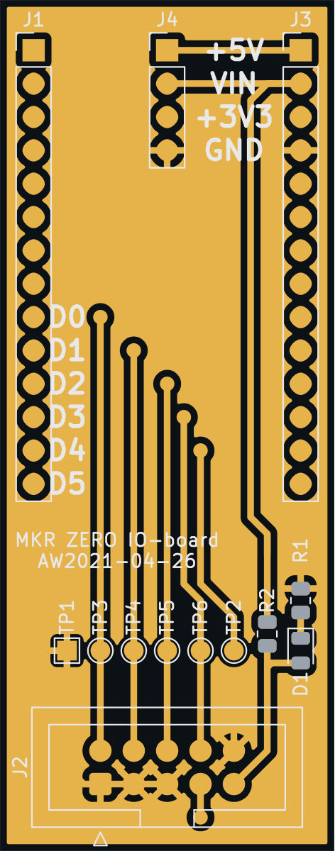
MICROSTEPPER MKR IO (OHWR0078 R1) is an open-hardware circuit board from the CERN Open Hardware Repository, designed in KiCad EDA: a 2-layer board of 25.4 × 64.8 mm with 13 components and 31 nets, published under CERN-OHL-S-2.0.
review complete · 1 item need the designer's input · 5 findings: 1 major · 4 minor (6 items)
Open in the interactive viewerRead the full review
Design review
Probe recorded 5 findings: 1 major · 4 minor (6 items) on this design. Each is shown here with its reasoning; the full review links every one to the pins, nets and datasheet pages it rests on.
- ReferencePlaneDiscontinuitymajorOpen
Tracks on B.CU and F.CU cross each other at 10 places, each layer the other's reference with its pour cleared round its own tracks, the longest 4.69 mm; 1 runs ALONG the cut round another net's track (fastest: CS1_DDSA at 100 ps 10-90 %, ASSUMED)
B.CU and F.CU each carry a pour and routed tracks, and each is the other's nearest reference. Wherever a track on one crosses a track on the other, the pour under it is cleared round that other track, so for the width of the cut the return has no plane under it and detours round the cut. 10 place(s) on 5 net(s), 9 of them seen from both tracks (each counted once). 1 of the crossings run ALONG the cut round another net's track rather than across it, parallel to its edges (the longest 2.58 mm): over or right beside that track, broadside to it as well as off the plane. One decision covers the layer pair: whether these layers may take a pour their own tracks cut as the reference, or the routing or the stackup should give the tracks a plane that is not cut where they cross. No crossing has a plane on the track's other side, so the whole return meets the break.
- 'CS3_PLL' on B.CU at (132.86, -131.94), 4.69 mm, running ALONG the bare copper for 2.58 mm, not across it over copper of DC_5V, not a plane; other side: none: the signal layer is outermost
- one crossing of two tracks, seen from each: 'CS1_DDSA' on F.CU at (125.24, -110.48), 1.52 mm over copper of CS3_PLL, not a plane; other side: none: the signal layer is outermost / 'CS2_DDSB' on F.CU at (126.51, -110.48), 1.52 mm over copper of CS3_PLL, not a plane; other side: none: the signal layer is outermost / 'CS3_PLL' on B.CU at (125.88, -110.48), 2.75 mm over copper of CS1_DDSA, CS2_DDSB, not a plane, to the end of the track; other side: none: the signal layer is outermost
- one crossing of two tracks, seen from each: 'CS1_DDSA' on B.CU at (120.16, -105.4), 1.52 mm over copper of SCK, not a plane; other side: none: the signal layer is outermost / 'SCK' on F.CU at (120.16, -105.4), 1.52 mm over copper of CS1_DDSA, not a plane; other side: none: the signal layer is outermost
- one crossing of two tracks, seen from each: 'CS1_DDSA' on B.CU at (122.7, -105.4), 1.52 mm over copper of SIO, not a plane; other side: none: the signal layer is outermost / 'SIO' on F.CU at (122.7, -105.4), 1.52 mm over copper of CS1_DDSA, not a plane; other side: none: the signal layer is outermost
- one crossing of two tracks, seen from each: 'CS1_DDSA' on F.CU at (125.24, -107.94), 1.52 mm over copper of CS2_DDSB, not a plane; other side: none: the signal layer is outermost / 'CS2_DDSB' on B.CU at (125.24, -107.94), 1.48 mm over copper of CS1_DDSA, not a plane, to the end of the track; other side: none: the signal layer is outermost
- one crossing of two tracks, seen from each: 'CS2_DDSB' on B.CU at (120.16, -107.94), 1.52 mm over copper of SCK, not a plane; other side: none: the signal layer is outermost / 'SCK' on F.CU at (120.16, -107.94), 1.52 mm over copper of CS2_DDSB, not a plane; other side: none: the signal layer is outermost
- one crossing of two tracks, seen from each: 'CS2_DDSB' on B.CU at (122.7, -107.94), 1.52 mm over copper of SIO, not a plane; other side: none: the signal layer is outermost / 'SIO' on F.CU at (122.7, -107.94), 1.52 mm over copper of CS2_DDSB, not a plane; other side: none: the signal layer is outermost
- one crossing of two tracks, seen from each: 'CS3_PLL' on B.CU at (120.16, -110.48), 1.52 mm over copper of SCK, not a plane; other side: none: the signal layer is outermost / 'SCK' on F.CU at (120.16, -110.48), 1.52 mm over copper of CS3_PLL, not a plane; other side: none: the signal layer is outermost
- one crossing of two tracks, seen from each: 'CS3_PLL' on B.CU at (122.7, -110.48), 1.52 mm over copper of SIO, not a plane; other side: none: the signal layer is outermost / 'SIO' on F.CU at (122.7, -110.48), 1.52 mm over copper of CS3_PLL, not a plane; other side: none: the signal layer is outermost
- one crossing of two tracks, seen from each: 'SCK' on F.CU at (120.16, -102.86), 1.52 mm over copper of SIO, not a plane; other side: none: the signal layer is outermost / 'SIO' on B.CU at (120.16, -102.86), 1.52 mm over copper of SCK, not a plane; other side: none: the signal layer is outermost
Every site is a row of this finding's evidence, keyed by net, layers and position. GET /api/odb/boards/2/reference-planes?group=void%3Arouted%40B.CU%7CF.CU serves each with its own layer_image region; all of them lie in x 118.4..133.86, y -135.42..-101.1 mm (board frame, Y up).
Read from the copper as drawn on the reference layer, along each track's centreline at exact breakpoints. The reference is the copper beside the track, never the layer's type or name. Whether it matters depends on each signal's edge rate, which nothing on file states for these nets: a slow static line crosses a split harmlessly, a fast edge does not.
At void:routed@B.CU|F.CU
MKR IO schematic title block leaves Rev and Date blank
The MKR IO schematic title block leaves Rev and Date blank, so a printed schematic cannot be matched to a board revision.
The only sheet (mkr_ioboard.kicad_sch, 1/1) reads 'Title: Arduino MKR ZERO to 10pin IDC adapterboard', 'Size: A4', 'Id: 1/1', with 'Date:' and 'Rev:' empty. The PCB silk carries 'AW2021-04-26', but the schematic carries no date or revision.
MKR IO schematic does not show the Arduino MKR headers J1, J3 or the power header J4
The MKR IO schematic does not draw the Arduino MKR headers J1 and J3 or the power header J4, so the mapping of the DDS control lines to Arduino D0..D4 can only be checked from the layout.
On the schematic on file (page 1, the only sheet) the labels SCK, SIO, CS1_DDSA, CS2_DDSB, CS3_PLL and +5V, VIN, +3V3, GND, RESET, MKR_MISO, MKR_SCK, MKR_MOSI end in wires that stop in empty space. Only free text 'D0'..'D5' stands beside them. No symbol, reference designator or pin number is drawn for J1, J3 or J4; the sheet's netlist slice lists J2, R1, R2, D1 and TP1-TP6 only.
What the PCB has
The PCB places all three (J1/J3 1x14 2.54 mm headers, J4 1x4) and routes these nets to them, for example:
Header Pins J1 9 = SCK, 10 = SIO, 11 = CS1_DDSA, 12 = CS2_DDSB, 13 = CS3_PLL J3 1..5 = +5V, VIN, +3V3, GND, RESET J4 1..4 = +5V, VIN, +3V3, GND - ConnectorDomainMixedminorOpen
ConnectorDomainMixed: 2 components×2
Checked by the review, stands · Claude walker W3 (Cern session) — Checked: several supplies leave on one connector, as the netlist shows. Whether that is a designed power interface or a hazard is the designer's intent; no standard contact map is on file to retire it. Left for the owner.
At J3, J4
Each finding, with its own headline
J3J3 takes 3 different supplies off the board on one connector: +5V (5.0 V), VIN (5.0 V), +3V3 (3.3 V)
J3 carries 3 different supplies out of the board on one connector: +5V (5.0 V) on 1, VIN (5.0 V) on 2, +3V3 (3.3 V) on 3. Declare the intent. Two rails on one connector is ordinary in a docking or power-distribution interface and a hazard in a signal one, and the difference is not visible from the netlist — but note that adjacent contacts at different voltages are exactly what a mirrored, reversed or off-by-one cable shorts together, so the cost of getting the mating wrong is a rail collision rather than a dead signal. If this is a standard connector, declare its family (connector_family_declare) and file the standard's contact map: supplies on the contacts it assigns to power are then not reported.
J4J4 takes 3 different supplies off the board on one connector: +5V (5.0 V), VIN (5.0 V), +3V3 (3.3 V)
J4 carries 3 different supplies out of the board on one connector: +5V (5.0 V) on 1, VIN (5.0 V) on 2, +3V3 (3.3 V) on 3. Declare the intent. Two rails on one connector is ordinary in a docking or power-distribution interface and a hazard in a signal one, and the difference is not visible from the netlist — but note that adjacent contacts at different voltages are exactly what a mirrored, reversed or off-by-one cable shorts together, so the cost of getting the mating wrong is a rail collision rather than a dead signal. If this is a standard connector, declare its family (connector_family_declare) and file the standard's contact map: supplies on the contacts it assigns to power are then not reported.
- FiducialMissingminorOpen
The top side carries 3 SMT component(s) and no fiducial was found on it
The top side carries 3 SMT component(s) but no fiducial was found on it — a placement machine has no optical reference to align to. Probe found no pad labelled .pad_usage=g_fiducial/l_fiducial (basis pad_usage); no single-pad, netless, undrilled component whose 0.5-3 mm round pad has a concentric solder-mask opening at least 1.5x its diameter with no other copper inside it (basis geometry); and no component whose refdes starts FID or whose part or package name contains FIDUCIAL (basis footprint-name). If your library names fiducials something Probe does not recognise, mark this benign — disposition_finding(rule='FiducialMissing', entity='top', status='benign', reason=…) — the name match only ever silences this check, it never asserts anything. If the side really has no fiducial, say so with status='confirmed': that answers the finding and keeps it gating release. Graded minor: the side carries only 3 SMT part(s) (at most 5), which a placement machine can usually align on their own pads; a fine-pitch part among them would still want one.
At top
About this design
- Design
- MICROSTEPPER MKR IO — OHWR0078 R1
- Designed in
- KiCad EDA
- Board
- 2 copper layers, 25.4 × 64.8 mm, 13 components, 31 nets
- Licence
- CERN-OHL-S-2.0
- Source
- https://gitlab.com/ohwr/project/microstepper at commit
46ae03051ab5 - Attribution
- CERN Open Hardware Repository, project microstepper (path mkr_ioboard/), commit 46ae03051ab5b384582b0fa5100d2e5447509ebe (2025-04-08). Licence: CERN-OHL-S-2.0. Source: https://gitlab.com/ohwr/project/microstepper. This is a snapshot of the copy published on the OHWR GitLab pages (R1), not CERN's released record. CERN's source of truth is EDMS (https://edms.cern.ch), and the current release may be newer.
- Reviewed with
- Probe by E# (E-Sharp AB)