 Probe

P4CH LNLS
OHWR0059 · revision R1
P4CH LNLS (OHWR0059 R1) is an open-hardware circuit board from the CERN Open Hardware Repository, designed in Altium Designer: a 4-layer board of 223.3 × 160.3 mm with 827 components and 372 nets, published under CERN-OHL-S-2.0.
review 81% walked · 26 findings: 4 blocker · 15 major · 7 minor (80 items)
Open in the interactive viewerRead the full review
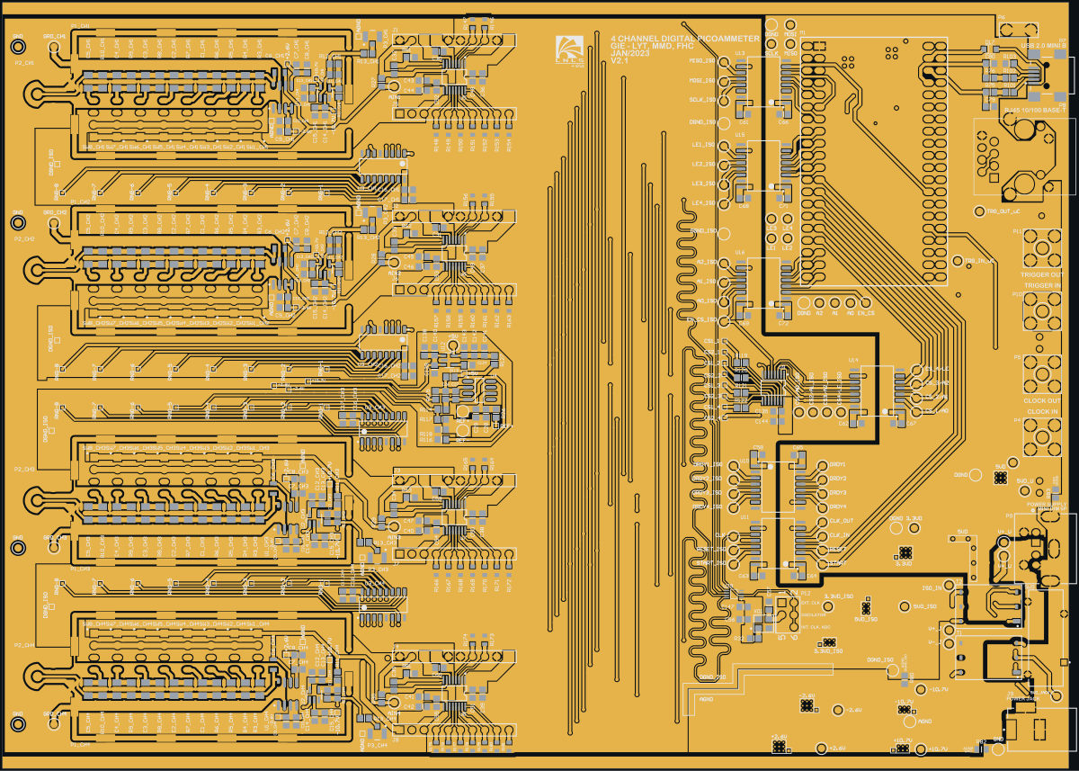
Design review
Probe recorded 26 findings: 4 blocker · 15 major · 7 minor (80 items) on this design. Each is shown here with its reasoning; the full review links every one to the pins, nets and datasheet pages it rests on.
- NetCopperSplitblockerOpen
NetJ9_1's copper is in 2 pieces: R108.2 is not connected to the rest of the net
NetJ9_1's copper is in 2 pieces: R108.2 is not connected to the rest of the net. Piece 1: J9.1, on TOP_LAYER, over (210.2, 6.1) to (212.2, 10.1). Piece 2: R108.2, on BOTTOM_LAYER, over (210.2, 6.1) to (217.93, 12.15). The export files every one of these pins under the net, so every connectivity check passes; the copper the fab builds leaves them apart. Usually a pour island that touches only one via of its own net, or a track ending short of its copper: join the piece to the net and export again.
At split:NetJ9_1
- PowerGroundShortblockerOpen
PowerGroundShort: 2 nets×2
Checked by the review, stands · evaluation@esharp.se — Checked; stands as a BOM-level issue for the owner. Schematic p.6 (Reference Voltage, ADR441 U4) draws three pairs of 0R assembly-option jumpers: R114 (-2.6V) / R116 (AGND) select U4's ground, R117 (-2.6V) / R118 (AGND) select the ADC reference REF-, and R115 (+2.6V) / R113 (+5V) select U4's VIN. Each pair is evidently meant to have ONE jumper fitted, but the sheet says 'Variant: [No Variations]' and the source BOM lists all six as fitted RC0805JR-070RL 0 ohm (one line of 59 jumpers), so as specified -2.6V is shorted to AGND through R114+R116 and through R117+R118 (and +2.6V to +5V through R115+R113). Either the BOM must mark one jumper of each pair not fitted, or the board shorts its negative analog supply. A person must decide which option the design intends.
At -2.6V
Each finding, with its own headline
-2.6V'-2.6V' is shorted to 'NetC26_1' through fitted link(s) R114
'-2.6V' is shorted to 'NetC26_1' through fitted zero-ohm link(s) R114: -2.6V -> R114 -> NetC26_1. Every link on that path is populated, so this is a direct rail-to-ground path in the build as specified. No pin role is involved and none would help — a two-terminal link has no datasheet pin function — which is why the role-layer axis of this check cannot see it. If these are a two-position option network, exactly one link per position should be fitted and the other marked DNP.
-2.6V'-2.6V' is shorted to 'AGND' through fitted link(s) R117, R118
'-2.6V' is shorted to 'AGND' through fitted zero-ohm link(s) R117, R118: -2.6V -> R117 -> REF- -> R118 -> AGND. Every link on that path is populated, so this is a direct rail-to-ground path in the build as specified. No pin role is involved and none would help — a two-terminal link has no datasheet pin function — which is why the role-layer axis of this check cannot see it. If these are a two-position option network, exactly one link per position should be fitted and the other marked DNP.
- PowerRailConflictblockerOpen
PowerRailConflict: 4 components×4
4 checked by the review by Claude walker W1 (Cern session) — 4 different reasons
At R132, R133, R134, R135
Each finding, with its own headline
R132R132 bridges different-voltage rails: V-_AD1 (-2.628V), -10.7V (-10.656V)
R132 (2-pin resistor) bridges different-voltage rails: V-_AD1 (-2.628V), -10.7V (-10.656V) — rail-to-rail short?
R133R133 bridges different-voltage rails: V-_AD2 (-2.628V), -10.7V (-10.656V)
R133 (2-pin resistor) bridges different-voltage rails: V-_AD2 (-2.628V), -10.7V (-10.656V) — rail-to-rail short?
R134R134 bridges different-voltage rails: V-_AD3 (-2.628V), -10.7V (-10.656V)
R134 (2-pin resistor) bridges different-voltage rails: V-_AD3 (-2.628V), -10.7V (-10.656V) — rail-to-rail short?
R135R135 bridges different-voltage rails: V-_AD4 (-2.628V), -10.7V (-10.656V)
R135 (2-pin resistor) bridges different-voltage rails: V-_AD4 (-2.628V), -10.7V (-10.656V) — rail-to-rail short?
- PowerRailConflictblockerOpen
PowerRailConflict: 5 components×5
Checked by the review, stands · Claude walker W1 (Cern session) — Checked: R113 and R140-R143 are the 0 ohm supply-option links, and the BOM fits both links of each pair with no variant, so +10.7V really is tied to the ADC +2.6V rails and +5V to +2.6V. Real, and raised for CERN as OBS-543; left for the owner.
At R113, R140, R141, R142, R143
Each finding, with its own headline
R113R113 bridges different-voltage rails: +5V (5.0V), NetC26_2 (2.589V)
R113 (2-pin resistor) bridges different-voltage rails: +5V (5.0V), NetC26_2 (2.589V) — rail-to-rail short?
R140R140 bridges different-voltage rails: +10.7V (10.755V), V+_AD1 (2.589V)
R140 (2-pin resistor) bridges different-voltage rails: +10.7V (10.755V), V+_AD1 (2.589V) — rail-to-rail short?
R141R141 bridges different-voltage rails: +10.7V (10.755V), V+_AD2 (2.589V)
R141 (2-pin resistor) bridges different-voltage rails: +10.7V (10.755V), V+_AD2 (2.589V) — rail-to-rail short?
R142R142 bridges different-voltage rails: +10.7V (10.755V), V+_AD3 (2.589V)
R142 (2-pin resistor) bridges different-voltage rails: +10.7V (10.755V), V+_AD3 (2.589V) — rail-to-rail short?
R143R143 bridges different-voltage rails: +10.7V (10.755V), V+_AD4 (2.589V)
R143 (2-pin resistor) bridges different-voltage rails: +10.7V (10.755V), V+_AD4 (2.589V) — rail-to-rail short?
ADS1246 split supply ±2.6V sits 22-33 mV inside the recommended limits; regulator tolerance can take it outside
The four ADS1246 converters (U5-U8) run from AVDD = +2.6V (U27, LT1762) and AVSS = -2.6V (U28, TPS7A3401). With the fitted feedback resistors the nominal rails are +2.589 V and -2.628 V. That leaves only 22 mV to the ADS1246 recommended AVSS-to-DGND minimum and 33 mV to the AVDD-to-AVSS maximum. The regulators' own reference tolerances, plus 1% resistors, can take both quantities outside the recommended operating range. They stay inside absolute maximum.
Rails as built
- +2.6V: U27 LT1762 ADJ, R94 = 5.6k (OUT to ADJ), R95 = 4.99k (ADJ to AGND). Vout = 1.22 V x (1 + 5.6/4.99) = 2.589 V. Reaches the ADCs through 0R R98.
- -2.6V: U28 TPS7A3401, R96 = 10k (OUT to FB), R97 = 8.2k (FB to AGND). Vout = -1.184 V x (1 + 10/8.2) = -2.628 V. Reaches the ADCs through 0R R99.
- ADS1246 DGND is on DGND_ISO. AGND is tied to DGND_ISO by R80, which the power sheet's "Ground Connection" note marks as connected.
Against the ADS1246 recommended operating conditions (datasheet p.8)
Quantity Limit (recommended) Nominal on board Margin Tolerance-stack extreme Abs max (p.7) AVSS to DGND >= -2.65 V -2.628 V 22 mV about -2.698 V -2.8 V AVDD to AVSS <= 5.25 V 5.217 V 33 mV about 5.379 V 5.5 V The extremes combine these datasheet limits:
- LT1762 ADJ pin voltage 1.190-1.250 V over line, load and temperature (LT1762 datasheet p.3).
- TPS7A3401 internal reference -1.166 to -1.202 V at 25 C (p.5). Overall accuracy is ±2.5 %.
- 1% feedback resistors, from the BOM part numbers RC0805FR-07*.
Why it matters
Outside the recommended range the ADS1246's specifications are not guaranteed. The part is not damaged, because absolute maximum still holds. The TI part is characterised for a ±2.5 V split supply. The board also uses AVSS as REFN, because the ADR441 reference is lifted onto -2.6V.
``
mermaid flowchart LR U27[U27 LT1762 +2.589V nom] --R98 0R--> AVDD[ADS1246 AVDD x4] U28[U28 TPS7A3401 -2.628V nom] --R99 0R--> AVSS[ADS1246 AVSS x4] AGND --R80 0R--> DGND_ISO[ADS1246 DGND]``Not refuted by
- No trim and no tighter-tolerance resistors are on the BOM.
- The schematic resistor table ("Table 2: Resistor selection for +/-2.6V") shows the same values, so this is the intended setpoint.
- A lower setpoint, for example ±2.5 V, would restore margin. The ADR441 would still have headroom: VIN-GND of 5.0 V against the 3.0 V minimum.
U12 REG113 is fed from +10.7V, above its 10 V operating input limit
U12 (REG113NA-5, the +5V LDO) takes its input directly from the +10.7V rail. That rail is set to 10.76 V nominal and can reach about 11.2 V. The REG113 operating input range ends at 10 V and its absolute maximum is 12 V. So the part runs above its operating range at all times, and is within about 0.8 V of absolute maximum at the rail's tolerance extreme.
Connectivity
- U12 pin 1 (VIN) and pin 3 (Enable) are on +10.7V. Pin 5 (VOUT) feeds +5V through R127 0R.
- +10.7V is the output of U23 (LT1762 ADJ) through R91 0R. The feedback is R86 = 39k from OUT to ADJ and R89 = 4.99k from ADJ to AGND.
- Vout(U23) = 1.22 V x (1 + 39/4.99) = 10.76 V nominal. The worst-case high, with ADJ 1.250 V and 1% resistors, is 1.25 x (1 + 39.39/4.94) = 11.2 V.
Against the REG113 datasheet
Quantity Limit Actual Margin VIN, operating range (p.3) 1.8 to 10 V 10.76 V nom / 11.2 V max -0.76 V (nominal already over) VIN, absolute maximum (p.2) 12 V 11.2 V max 0.8 V ``
mermaid flowchart LR VP[V+ 11.3-14.5 V] --> U23[U23 LT1762 ADJ R86 39k / R89 4.99k] U23 --R91 0R--> R107[+10.7V rail 10.76 V nom] R107 --> U12[U12 REG113-5 VIN max 10 V operating] U12 --R127 0R--> P5[+5V]``Notes
- The schematic's own table names this rail "+10.7V" and lists U12 under "LN Regulator +10.7V/+5V", so the input voltage is intended, not a mis-set divider.
- Outside the operating range the REG113 specifications do not apply. The margin to absolute maximum is small at the tolerance extreme.
- Per the ADC sheet, the +5V rail is used by the ADS125H01 build option (J5-J8 pin 1, and R113 to the ADR441). U12 is on the BOM as fitted. If U12 is not fitted in the ADS1246 build, this does not apply to that build. The BOM carries no fit status.
- Options for the designer: a 5 V LDO rated to more than 11.2 V input, a series pre-drop, or feeding U12 from a lower rail.
Trigger-in termination R1||R2 (60 ohm, 2x 1/2 W) is overloaded above ~7.7 V, but the sheet states 3.3-27 V input
The trigger input TRG_IN (SMA P10) is terminated to DGND_OPTO by R1 and R2, each 120 ohm, 1/2 W, 1210, in parallel: 60 ohm. The Microcontroller sheet states "Trigger In - Operating Voltage Range: 3.3V to 27V". At 27 V each resistor would dissipate 6.1 W, twelve times its rating. The resistors reach their 0.5 W rating at only 7.75 V. The termination and the stated input range cannot both hold.
Connectivity
- P10.1 is TRG_IN; P10.2 is DGND_OPTO.
- R1 and R2 each connect TRG_IN to DGND_OPTO.
- TRG_IN also feeds D9 (TVS) and R69 300R, then D11 (NSI50010 10 mA CCR) and the U19 FOD8160 LED.
Numbers
Input on TRG_IN Power per resistor (V^2/120) Rating (BOM: "RES SMD 120 OHM 1% 1/2W 1210") Margin 3.3 V 0.09 W 0.5 W OK 5 V 0.21 W 0.5 W OK 7.75 V 0.50 W 0.5 W 0 12 V 1.2 W 0.5 W 2.4x over 27 V (stated max) 6.1 W 0.5 W 12x over A 27 V driver would also have to source 450 mA into the 60 ohm termination.
``
mermaid flowchart LR P10[P10 SMA TRG_IN] --> R1[R1 120R 1/2W] --> G[DGND_OPTO] P10 --> R2[R2 120R 1/2W] --> G P10 --> R69[R69 300R] --> D11[D11 CCR 10mA] --> U19[U19 FOD8160 LED] --> G``Interpretation
R1||R2 looks like a 50-60 ohm termination for a low-voltage (TTL/LVTTL) trigger source. The CCR front end (D11) is what makes a 3.3-27 V range possible, and it only works as a wide-range input if the termination is not fitted. The BOM lists R1/R2 as fitted, and the sheet's "Standart Connection" note covers only D11/R72. Either the input range note or the termination fit needs qualifying. This depends on R1/R2 being fitted, which the BOM as published says they are.
Trigger-in CCR D11 (NSI50010) dissipates ~0.23-0.28 W at the stated 27 V input, above its 208-227 mW small-copper rating
D11 (NSI50010YT1G, a 10 mA constant-current regulator) sets the U19 opto-LED current on the trigger input. The sheet states the input can be 3.3-27 V, and the CCR drops everything the resistor and LED do not. At a steady 27 V it dissipates about 0.23 W, or up to 0.28 W at its 13 mA maximum. That exceeds the datasheet's steady-state dissipation rating for 100 mm2 of copper (208 mW at 25 C). With the datasheet's thermal resistances, the junction passes 150 C at room temperature unless D11 has several hundred mm2 of copper.
Path
TRG_IN (P10) -> R69 300R -> D11 anode (pin 1) -> D11 cathode (pin 2) -> U19 FOD8160 LED (pin 1 -> pin 3) -> DGND_OPTO. R72 0R, which would bypass D11, is marked "not connected" in the sheet's "Standart Connection" note, and D11 is marked connected.
Numbers (Vin = 27 V, the stated maximum)
Ireg (datasheet p.2: 7.0 / 10 / 13 mA) Vak = 27 - I*300 - VF(1.45 V, FOD8160 p.6) P(D11) 7 mA 23.5 V 0.16 W 10 mA 22.6 V 0.23 W 13 mA 21.7 V 0.28 W Copper (datasheet p.3) PD at 25 C thetaJA Tj at 0.23 W, Ta = 25 C Tj at 0.23 W, Ta = 70 C 100 mm2, 1 oz (Note 5) 208 mW 600 C/W 160 C 205 C 300 mm2, 1 oz (Note 8) 368 mW 340 C/W 103 C 148 C 500 mm2, 2 oz (Note 10) 463 mW 270 C/W 87 C 132 C Tj max = 150 C (p.2).
``
mermaid flowchart LR P10[TRG_IN 3.3-27 V] --> R69[R69 300R] --> D11[D11 NSI50010 10 mA CCR] --> LED[U19 FOD8160 LED] --> G[DGND_OPTO]``Limits of this finding
- This is steady-state dissipation. A low-duty-cycle pulse trigger dissipates proportionally less on average. The datasheet's steady-state figures apply to a level held high.
- The copper area around D11 on the bottom side was not measured.
- A wide input range is only reachable if R1/R2 are not fitted (see OBS-60). With R1/R2 fitted, the input is practically limited to about 7.7 V, where D11 dissipates about 30 mW.
LDS3985 U22/U26 outputs carry ~481-485 uF, 22x the datasheet's 2.2-22 uF output-capacitor range
Both 3.3 V LDOs are LDS3985M33R: U22 (5VD to 3.3VD) and U26 (5VD_ISO to 3.3VD_ISO). The datasheet specifies the output capacitor as 2.2 to 22 uF with ESR 5 to 5000 mOhm. Each output carries a 470 uF tantalum (C101 / C125, 293D477X96R3D2TE3) directly on the VOUT pin, plus ceramics. That totals about 481 uF on 3.3VD and 485 uF on 3.3VD_ISO, about 22x the specified maximum. The datasheet gives no stability or start-up data outside that range.
Output capacitance (from connectivity + BOM, including through 0R R90 / R100)
Rail Regulator Bulk on VOUT node Total C to ground Datasheet range (p.7) Over max 3.3VD U22 pin 5 C101 470 uF tant, C103 10 uF, C106 100 nF, C107 1 nF ~481 uF 2.2-22 uF 21.9x 3.3VD_ISO U26 pin 5 C125 470 uF tant, C126 10 uF, C127 100 nF, C128 1 nF ~485 uF 2.2-22 uF 22.1x The ceramics on the far side of R90/R100 (8 x 100 nF on 3.3VD; 1 uF x4 + 100 nF on 3.3VD_ISO) are included.
Start-up consequence
The typical turn-on time is 240 us (p.7, with COUT = 2.2 uF and CBYP = 33 nF; CBYP here is 10 nF, C93/C131). Ramping 481 uF to 3.3 V in that time would take about 6.6 A, against a short-circuit current of 600 mA typ (p.7). So start-up is current-limited, taking about 481 uF x 3.3 V / 0.6 A = 2.6 ms or more, with the LDO in limit throughout. For U26 this inrush is drawn from 5VD_ISO, which is itself the output of U24 (REG113, foldback short-circuit limit 200 mA typ).
``
mermaid flowchart LR 5VD --> U22[U22 LDS3985 COUT spec 2.2-22 uF] --> N1[NetC101_1: C101 470uF + 10uF + ...] --R90 0R--> V33[3.3VD] 5VD_ISO --> U26[U26 LDS3985] --> N2[NetC125_1: C125 470uF + 10uF + ...] --R100 0R--> V33I[3.3VD_ISO]``Notes
- The ESR of a 470 uF 293D tantalum sits inside the 5-5000 mOhm window, so only the capacitance is outside the specification.
- The bulk may be intended as hold-up or low-frequency reservoir. If so, it would be within specification behind a small series resistance or moved to the LDO input side. Either way it is outside the conditions ST specifies for this LDO and worth a bench check of start-up and transient behaviour.
P4CH LNLS: 6.3 V tantalums C73, C84, C96, C111, C132 run at about 80% of rated on 5 V rails (C101, C125 at 52% on 3.3 V)
Seven 470 uF 6.3 V tantalums (electrolyte not stated) sit on 5 V and 3.3 V rails at 52-80% of their rating. If they are MnO2 parts, that is above the 50% manufacturers recommend, and an under-derated MnO2 tantalum can fail short and burn.
The numbers
Part Rail Rail voltage Applied / 6.3 V Source C73, C84 5VD 5 V 79% netlist; the rail feeds U22/U26 LDS3985M33R and U21 MAX253 C111 U24 REG113NA-5 output 5 V 79% netlist (U24 pin 5) C132 node after D19/R107 on the 5 V side about 5 V about 79% netlist C96 node after D15/D16 (rectified, upstream of the 5 V regulator) at least 5 V 79% or more netlist C101 U22 LDS3985M33R output 3.3 V 52% netlist (U22 pin 5) C125 U26 LDS3985M33R output 3.3 V 52% netlist (U26 pin 5) Rating: 470 uF 6.3 V 2917 tantalum, from the BOM line 'CAP TANT 470UF 10% 6.3V 2917'.
MnO2 tantalum limit (capacitor guide, citing KEMET T491 p.14, Vishay 40246/EIA-809, AVX TDS-PTNO-0024 1.2.2): about 50% of rated up to 85 C. A polymer tantalum rated 10 V or less is allowed 90% (KEMET T2076 p.32-33).
Depends on the electrolyte
The BOM gives only 'CAP TANT', with no manufacturer part number. If these are 6.3 V polymer parts (90% allowed), 5 V passes. If they are MnO2, it does not. Fix: name a polymer part, or use 10 V parts on the 5 V rails.
Orientation is correct on all seven (+ on the rail).
LDS3985 LDOs U22 and U26 carry 470 µF on their outputs, above the 22 µF maximum in the datasheet
U22 and U26 (ST LDS3985M33R, 3.3 V) each have a 470 µF tantalum plus a 10 µF ceramic on the output, more than 20 times the 22 µF maximum output capacitance ST specifies for stable operation.
Item Value Source Output capacitor, recommended range 2.2 µF to 22 µF LDS3985 datasheet p.7 (electrical characteristics) Output capacitor ESR range 5 mΩ to 5000 mΩ same U22 output (NetC101_1) C101 470 µF 6.3 V tantalum (293D477X96R3D2TE3) + C103 10 µF X7R + 100 nF + 1 nF netlist, BOM U26 output (NetC125_1) C125 470 µF (same part) + C126 10 µF X7R + 100 nF + 1 nF netlist, BOM Why it matters
Outside the specified range ST does not guarantee loop stability. A large output capacitance also slows start-up, and the 300 mA current limit has to charge it (soft-start and power-good timing).
The same 470 µF part on U24 (a REG113, stable with any output capacitance) is fine. Fix: move the bulk capacitor ahead of the LDO, or use an LDO rated for large output capacitance.
BOM fits both 0R links of every supply-option pair (no variant): +/-10.7V tied to +/-2.6V, +5V to +2.6V, -2.6V to AGND
The published BOM fits every 0R option link on the P4CH board, and the schematic has no variant, so built as documented it ties LDO outputs together: +10.7V to +2.6V, -10.7V to -2.6V, +5V to +2.6V and -2.6V to AGND.
The schematic offers two alternative supply sets for the ADC: the ADS1246 set (+/-2.6V) and the ADS125H01 set (+/-10.7V and +5V). Each choice is made with pairs of 0R links that land on the same net. The design data does not record which link of each pair to leave off.
The paired links
Net they share Link to option A Link to option B Source V+_AD1..4 (J5-J8 pin 3) R136-R139 to +2.6V R140-R143 to +10.7V ADC sheet (sheet 6), netlist V-_AD1..4 (J5-J8 pin 2) R111, R129-R131 to -2.6V R132-R135 to -10.7V ADC sheet (sheet 6), netlist ADR441 U4 VIN (NetC26_2) R115 to +2.6V R113 to +5V ADC sheet, "Reference Voltage" ADR441 U4 GND (NetC26_1) R114 to -2.6V R116 to AGND ADC sheet, "Reference Voltage" REF- R117 to -2.6V R118 to AGND ADC sheet GND to AGND R82 ("Not Connected" per sheet note) - Power Supply sheet (sheet 8), "Ground Conection: Standard (bias off): R80, R83 Connected, R82 Not Connected" What the documents say is fitted
Document Statement Source Designer BOM One row, value 0, quantity 59, designators include all of R111, R113-R118, R129-R143 and R82; Mounted and Fitted columns empty on every row OHWR P4CH-LNLS BOM (commit 2a677998) Schematic "Variant: [No Variations]" ADC sheet title block area Fitted ADC U5-U8 ADS1246IPWR, so option A (+/-2.6V) is the configuration in use BOM Why it matters
Fitted as listed, each pair shorts one regulator output into another: LT1762 U23 (+10.7V) into LT1762 U27 (+2.6V), TPS7A3401 U25 (-10.7V) into U28 (-2.6V), REG113 U12 (+5V) into +2.6V, and the -2.6V rail straight to AGND. An assembler working from the published BOM has nothing that tells them otherwise. The R82 link would also join GND to AGND, against the sheet's own note.
``
mermaid graph LR U23[U23 LT1762 +10.7V] -->|R140 0R| VP[V+_AD1] U27[U27 LT1762 +2.6V] -->|R136 0R| VP U25[U25 TPS7A3401 -10.7V] -->|R132 0R| VN[V-_AD1] U28[U28 TPS7A3401 -2.6V] -->|R111 0R| VN``What would settle it
A fit list or Altium variant that marks, for the ADS1246 build, R136-R139, R111/R129-R131, R115, R114 and R117 fitted and R140-R143, R132-R135, R113, R116, R118 and R82 not fitted (or the reverse for the ADS125H01 build).
- DecapViaFanoutmajorOpen
C85 on '5VD': its rail pad reaches its via over 5.47 mm of track, adding about 2.37 nH to its loop, past Probe's 0.5 nH starting value; put the vias at the pads
C85 on '5VD': its rail pad reaches its via over 5.47 mm of track, adding about 2.37 nH to its loop, past Probe's 0.5 nH starting value; put the vias at the pads. C85.2 (rail) runs 5.47 mm along its copper to its nearest via, 4.47 mm past the 1 mm beside the pad: 2.37 nH; C85.1 (ground) not measured: the pad sits in a pour of its net on its own layer, which has no track length to measure. Each run past the pad as one conductor of a pair 1.80 mm apart (the pad pitch), 0.2 l ln(D/R) nH with R 0.127 mm (the track's width is not read): 2.37 nH in all. Put the vias at the pads (or in them), one per pad at least, the rail's and the ground's close together; the capacitor's own inductance as mounted is 0.77 nH (pad 0.10 nH + no via of the first net within 1 mm of its pad: the study's 0.6 nH per mm of 0.26 mm depth, ASSUMED). 0.5 nH is Probe's starting value, about the whole mounted inductance of a well-mounted 0402.
At C85
- FiducialMissingmajorOpen
FiducialMissing: 2 boards×2
2 checked by the review by evaluation@esharp.se — 2 different reasons
At bottom, top
Each finding, with its own headline
bottomThe bottom side carries 186 SMT component(s) and no fiducial was found on it
The bottom side carries 186 SMT component(s) but no fiducial was found on it — a placement machine has no optical reference to align to. Probe found no pad labelled .pad_usage=g_fiducial/l_fiducial (basis pad_usage); no single-pad, netless, undrilled component whose 0.5-3 mm round pad has a concentric solder-mask opening at least 1.5x its diameter with no other copper inside it (basis geometry); and no component whose refdes starts FID or whose part or package name contains FIDUCIAL (basis footprint-name). If your library names fiducials something Probe does not recognise, mark this benign — disposition_finding(rule='FiducialMissing', entity='bottom', status='benign', reason=…) — the name match only ever silences this check, it never asserts anything. If the side really has no fiducial, say so with status='confirmed': that answers the finding and keeps it gating release.
topThe top side carries 142 SMT component(s) and no fiducial was found on it
The top side carries 142 SMT component(s) but no fiducial was found on it — a placement machine has no optical reference to align to. Probe found no pad labelled .pad_usage=g_fiducial/l_fiducial (basis pad_usage); no single-pad, netless, undrilled component whose 0.5-3 mm round pad has a concentric solder-mask opening at least 1.5x its diameter with no other copper inside it (basis geometry); and no component whose refdes starts FID or whose part or package name contains FIDUCIAL (basis footprint-name). If your library names fiducials something Probe does not recognise, mark this benign — disposition_finding(rule='FiducialMissing', entity='top', status='benign', reason=…) — the name match only ever silences this check, it never asserts anything. If the side really has no fiducial, say so with status='confirmed': that answers the finding and keeps it gating release.
- PartLifecyclemajorOpen
NUP1128HT1G on D9: the distributor catalogue reports "Obsolete" for onsemi's NUP1128HT1G
NUP1128HT1G on D9: the distributor catalogue reports "Obsolete" for onsemi's NUP1128HT1G — a sourcing/longevity risk to confirm against the MANUFACTURER before acting. That is the maker this board's BOM names (onsemi). A distributor delisting is not the same claim as the part being unavailable; check the vendor's own lifecycle/product-change notice for the status and any named successor. Re-read the source: GET /api/odb/parts/NUP1128HT1G/providers (which provider said it, the maker and part number it matched, its own words, and when we asked). THE LAST BUY DATE HAS PASSED (2026-06-18, 150 day(s) ago), so this is a substitution rather than a buy. The distributor reports 1,564 left. No approved alternate is recorded for this position.
At D9
- PartLifecyclemajorOpen
PartLifecycle: 3 part numbers×3
2 Obsolete, 1 Discontinued at DigiKey · on 6 placements
At C5_CH1, P8, SW9
Each finding, with its own headline
C5_CH1CGJ5L2C0G1H104J160AA on 4 placements (C5_CH1, C5_CH2, C5_CH3, C5_CH4): the distributor catalogue reports "Obsolete" for TDK's CGJ5L2C0G1H104J160AA
CGJ5L2C0G1H104J160AA on 4 placements (C5_CH1, C5_CH2, C5_CH3, C5_CH4): the distributor catalogue reports "Obsolete" for TDK's CGJ5L2C0G1H104J160AA — a sourcing/longevity risk to confirm against the MANUFACTURER before acting. That is the maker this board's BOM names (TDK Corporation). A distributor delisting is not the same claim as the part being unavailable; check the vendor's own lifecycle/product-change notice for the status and any named successor. Re-read the source: GET /api/odb/parts/CGJ5L2C0G1H104J160AA/providers (which provider said it, the maker and part number it matched, its own words, and when we asked). THE LAST BUY DATE HAS PASSED (2023-11-30, 1,081 day(s) ago), so this is a substitution rather than a buy. The distributor reports NONE left. No approved alternate is recorded for this position.
P8J1B1211CCD on P8: the distributor catalogue reports "Discontinued at DigiKey" for WIZnet's J1B1211CCD
J1B1211CCD on P8: the distributor catalogue reports "Discontinued at DigiKey" for WIZnet's J1B1211CCD — a sourcing/longevity risk to confirm against the MANUFACTURER before acting. That is the maker this board's BOM names (WIZnet). A distributor delisting is not the same claim as the part being unavailable; check the vendor's own lifecycle/product-change notice for the status and any named successor. Re-read the source: GET /api/odb/parts/J1B1211CCD/providers (which provider said it, the maker and part number it matched, its own words, and when we asked). No approved alternate is recorded for this position.
SW9HE751A0510 on SW9: the distributor catalogue reports "Obsolete" for Littelfuse Inc.'s HE751A0510
HE751A0510 on SW9: the distributor catalogue reports "Obsolete" for Littelfuse Inc.'s HE751A0510 — a sourcing/longevity risk to confirm against the MANUFACTURER before acting. That is the maker this board's BOM names (Littelfuse Inc.). A distributor delisting is not the same claim as the part being unavailable; check the vendor's own lifecycle/product-change notice for the status and any named successor. Re-read the source: GET /api/odb/parts/HE751A0510/providers (which provider said it, the maker and part number it matched, its own words, and when we asked). No approved alternate is recorded for this position.
- ReferencePlaneDiscontinuitymajorOpen
ReferencePlaneDiscontinuity: 28 boards×28
Checked by the review, stands · Claude walker W1 (Cern session) — Checked: the 36 split/void/reference-change sites read from the copper stand; they are layout-practice findings with Probe's default limits, and no datasheet or app note on file sets one for these ADC, isolator and control nets. Left for the owner.
At along@INT2__PWR_:AGND|DGND, along@INT2__PWR_:DGND|DGND_ISO, refchange:+10.7V|AGND, refchange:+10.7V|DGND_ISO, refchange:-10.7V|AGND, refchange:-10.7V|DGND_ISO and 22 more
Each finding, with its own headline
along@INT2__PWR_:AGND|DGND'NetT2_1' runs ALONG the split between the AGND and DGND planes on INT2PWR_ at 1 place, the longest 3.28 mm; the impedance rises from 37 ohm to 49 ohm there at worst, 12.8 % of each edge reflected (fastest: NetT2_1 at 100 ps 10-90 %, ASSUMED)
On INT2__PWR_ the AGND and DGND planes part, and 'NetT2_1' runs down the slot between them at 1 place(s), rather than across it. This is not a crossing: the return still follows the track, in the plane on its other side and in the slot's edges, so it does not detour. What changes is the track's own impedance. With the plane gone from under it on this side for that length, its field reaches further, to the slot's edges and to the next plane beyond, so its capacitance falls and its impedance rises; every edge travelling down it is partly reflected where it enters the stretch and again where it leaves, by (Z2 - Z1)/(Z2 + Z1). The longer the stretch against the edge's rise, the more of the edge sees the full step. A crossing is generally the worse fault; a mismatch is not free. Over solid plane each track is 37 ohm; along the slot 49 ohm, reflecting up to 12.8 % of each edge (a method-of-moments field solve of the cross-section, one dielectric; were the slot's edges to carry none of the return, up to 71 ohm). No place stays within 10 %, the tolerance controlled impedance is commonly built to (the stackup states none), so the finding is a warning. One decision covers the split line's slot: whether these tracks may run down it, or should be moved over solid plane.
- 'NetT2_1' on BOTTOM_LAYER at (208.74, 30.75), 3.63 mm, running ALONG the split for 3.28 mm, not across it, 37 ohm over solid plane, 49 ohm along it: 12.8 % of each edge reflected; other side: none: the signal layer is outermost
Every site is a row of this finding's evidence, keyed by net, layers and position. GET /api/odb/boards/60/reference-planes?group=along%40INT2__PWR_%3AAGND%7CDGND serves each with its own layer_image region; all of them lie in x 206.1..211.63, y 29.75..32 mm (board frame, Y up).
Read from the copper as drawn on the reference layer, along each track's centreline at exact breakpoints. The reference is the copper beside the track, never the layer's type or name. Whether it matters depends on each signal's edge rate, which nothing on file states for these nets: a slow static line crosses a split harmlessly, a fast edge does not.
along@INT2__PWR_:DGND|DGND_ISO'CS1_2' runs ALONG the split between the DGND and DGND_ISO planes on INT2PWR_ at 1 place, the longest 5.2 mm; the impedance rises from 37 ohm to 43 ohm there at worst, 7.2 % of each edge reflected (fastest: CS1_2 at 100 ps 10-90 %, ASSUMED)
On INT2__PWR_ the DGND and DGND_ISO planes part, and 'CS1_2' runs down the slot between them at 1 place(s), rather than across it. This is not a crossing: the return still follows the track, in the plane on its other side and in the slot's edges, so it does not detour. What changes is the track's own impedance. With the plane gone from under it on this side for that length, its field reaches further, to the slot's edges and to the next plane beyond, so its capacitance falls and its impedance rises; every edge travelling down it is partly reflected where it enters the stretch and again where it leaves, by (Z2 - Z1)/(Z2 + Z1). The longer the stretch against the edge's rise, the more of the edge sees the full step. A crossing is generally the worse fault; a mismatch is not free. Over solid plane each track is 37 ohm; along the slot 43 ohm, reflecting up to 7.2 % of each edge (a method-of-moments field solve of the cross-section, one dielectric; were the slot's edges to carry none of the return, up to 71 ohm). No place stays within 10 %, the tolerance controlled impedance is commonly built to (the stackup states none), so the finding is a warning. One decision covers the split line's slot: whether these tracks may run down it, or should be moved over solid plane.
- 'CS1_2' on BOTTOM_LAYER at (165.15, 68.6), 5.83 mm, running ALONG the split for 5.2 mm, not across it, 37 ohm over solid plane, 43 ohm along it: 7.2 % of each edge reflected; other side: none: the signal layer is outermost
Every site is a row of this finding's evidence, keyed by net, layers and position. GET /api/odb/boards/60/reference-planes?group=along%40INT2__PWR_%3ADGND%7CDGND_ISO serves each with its own layer_image region; all of them lie in x 161.25..169.08, y 67.6..69.63 mm (board frame, Y up).
Read from the copper as drawn on the reference layer, along each track's centreline at exact breakpoints. The reference is the copper beside the track, never the layer's type or name. Whether it matters depends on each signal's edge rate, which nothing on file states for these nets: a slow static line crosses a split harmlessly, a fast edge does not.
refchange:+10.7V|AGND2 nets change reference between +10.7V and AGND at 2 vias, none with a reference that continues across (fastest: NetC11_CH3_2 at 100 ps 10-90 %, ASSUMED)
At 2 via(s), on 2 net(s), the signal leaves a layer referenced by one of +10.7V and AGND for a layer referenced by the other, and no plane references both layers. Different nets: no via can carry the return across; only decoupling between the two planes near the via can. The capacitor carrying the return across was measured at each via, at the knee of the crossing net's edge against 50 ohm assumed: 2 with none. 2 of them at an ASSUMED edge (no edge on file for the net): state one (net_timing_state) and it is re-read. One decision covers the pair: whether +10.7V and AGND are decoupled to each other near these vias. A via whose layers have more references than these two is a site of each pair it joins. None is partial: at every one, no reference continues across the via.
- 'NetC11_CH3_2' at (62.97, 49.63), TOP_LAYER -> BOTTOM_LAYER: AGND on INT1GND_ to +10.7V on INT2PWR_; pure, no reference continues across; stitching none, 7.5 mm of track past the via on BOTTOM_LAYER: At the 5 GHz knee of a 100 ps edge (100 ps 10-90 %, assumed: no edge is on file for the net) no capacitor carries the return; only the planes do. +10.7V and AGND are not a thin pair (at most 0.2 mm), so their own capacitance does not carry the return. To serve it, change layers across the same plane, or move the signal to a layer referenced to ground. None.
- 'NetC11_CH4_2' at (62.97, 12.8), TOP_LAYER -> BOTTOM_LAYER: AGND on INT1GND_ to +10.7V on INT2PWR_; pure, no reference continues across; stitching none, 7.5 mm of track past the via on BOTTOM_LAYER: At the 5 GHz knee of a 100 ps edge (100 ps 10-90 %, assumed: no edge is on file for the net) no capacitor carries the return; only the planes do. +10.7V and AGND are not a thin pair (at most 0.2 mm), so their own capacitance does not carry the return. To serve it, change layers across the same plane, or move the signal to a layer referenced to ground. None.
Every site is a row of this finding's evidence, keyed by net, layers and position. GET /api/odb/boards/60/reference-planes?group=refchange%3A%2B10.7V%7CAGND serves each with its own layer_image region; all of them lie in x 60.97..64.97, y 10.8..51.63 mm (board frame, Y up).
The reference on each layer is the first plane the track meets leaving the via, anti-pads and the net's own copper skipped. Whether it matters depends on each signal's edge rate, which nothing on file states for these nets: a slow static line crosses a split harmlessly, a fast edge does not.
refchange:+10.7V|DGND_ISO'SCLK_ISO' changes reference between +10.7V and DGND_ISO at a via, none with a reference that continues across (fastest: SCLK_ISO at 1 ns 10-90 %, suggested by its name)
At 1 via(s), on 1 net(s), the signal leaves a layer referenced by one of +10.7V and DGND_ISO for a layer referenced by the other, and no plane references both layers. Different nets: no via can carry the return across; only decoupling between the two planes near the via can. The capacitor carrying the return across was measured at each via, at the knee of the crossing net's edge against 50 ohm assumed: 1 with none. 1 of them at an ASSUMED edge (no edge on file for the net): state one (net_timing_state) and it is re-read. One decision covers the pair: whether +10.7V and DGND_ISO are decoupled to each other near these vias. A via whose layers have more references than these two is a site of each pair it joins. None is partial: at every one, no reference continues across the via.
- 'SCLK_ISO' at (118.87, 7.42), TOP_LAYER -> BOTTOM_LAYER: DGND_ISO on INT1GND_ to +10.7V on INT2PWR_; pure, no reference continues across; stitching none, 58.6 mm of track past the via on BOTTOM_LAYER: At the 5 GHz knee of a 100 ps edge (1 ns 10-90 %, assumed: no edge is on file for the net) no capacitor carries the return; only the planes do. +10.7V and DGND_ISO are not a thin pair (at most 0.2 mm), so their own capacitance does not carry the return. To serve it, change layers across the same plane, or move the signal to a layer referenced to ground. None.
Every site is a row of this finding's evidence, keyed by net, layers and position. GET /api/odb/boards/60/reference-planes?group=refchange%3A%2B10.7V%7CDGND_ISO serves each with its own layer_image region; all of them lie in x 116.87..120.87, y 5.42..9.42 mm (board frame, Y up).
The reference on each layer is the first plane the track meets leaving the via, anti-pads and the net's own copper skipped. Whether it matters depends on each signal's edge rate, which nothing on file states for these nets: a slow static line crosses a split harmlessly, a fast edge does not.
refchange:-10.7V|AGND2 nets change reference between -10.7V and AGND at 2 vias, none with a reference that continues across (fastest: NetC11_CH3_2 at 100 ps 10-90 %, ASSUMED)
At 2 via(s), on 2 net(s), the signal leaves a layer referenced by one of -10.7V and AGND for a layer referenced by the other, and no plane references both layers. Different nets: no via can carry the return across; only decoupling between the two planes near the via can. The capacitor carrying the return across was measured at each via, at the knee of the crossing net's edge against 50 ohm assumed: 2 with none. 2 of them at an ASSUMED edge (no edge on file for the net): state one (net_timing_state) and it is re-read. One decision covers the pair: whether -10.7V and AGND are decoupled to each other near these vias. A via whose layers have more references than these two is a site of each pair it joins. None is partial: at every one, no reference continues across the via.
- 'NetC11_CH3_2' at (70.15, 50.1), TOP_LAYER -> BOTTOM_LAYER: AGND on INT1GND_ to -10.7V on INT2PWR_; pure, no reference continues across; stitching none, 7.5 mm of track past the via on BOTTOM_LAYER: At the 5 GHz knee of a 100 ps edge (100 ps 10-90 %, assumed: no edge is on file for the net) no capacitor carries the return; only the planes do. -10.7V and AGND are not a thin pair (at most 0.2 mm), so their own capacitance does not carry the return. To serve it, change layers across the same plane, or move the signal to a layer referenced to ground. None.
- 'NetC11_CH4_2' at (70.15, 13.27), TOP_LAYER -> BOTTOM_LAYER: AGND on INT1GND_ to -10.7V on INT2PWR_; pure, no reference continues across; stitching none, 7.5 mm of track past the via on BOTTOM_LAYER: At the 5 GHz knee of a 100 ps edge (100 ps 10-90 %, assumed: no edge is on file for the net) no capacitor carries the return; only the planes do. -10.7V and AGND are not a thin pair (at most 0.2 mm), so their own capacitance does not carry the return. To serve it, change layers across the same plane, or move the signal to a layer referenced to ground. None.
Every site is a row of this finding's evidence, keyed by net, layers and position. GET /api/odb/boards/60/reference-planes?group=refchange%3A-10.7V%7CAGND serves each with its own layer_image region; all of them lie in x 68.15..72.15, y 11.27..52.1 mm (board frame, Y up).
The reference on each layer is the first plane the track meets leaving the via, anti-pads and the net's own copper skipped. Whether it matters depends on each signal's edge rate, which nothing on file states for these nets: a slow static line crosses a split harmlessly, a fast edge does not.
refchange:-10.7V|DGND_ISO2 nets change reference between -10.7V and DGND_ISO at 2 vias, none with a reference that continues across (fastest: CS2_4 at 100 ps 10-90 %, ASSUMED)
At 2 via(s), on 2 net(s), the signal leaves a layer referenced by one of -10.7V and DGND_ISO for a layer referenced by the other, and no plane references both layers. Different nets: no via can carry the return across; only decoupling between the two planes near the via can. The capacitor carrying the return across was measured at each via, at the knee of the crossing net's edge against 50 ohm assumed: 2 with none. 2 of them at an ASSUMED edge (no edge on file for the net): state one (net_timing_state) and it is re-read. One decision covers the pair: whether -10.7V and DGND_ISO are decoupled to each other near these vias. A via whose layers have more references than these two is a site of each pair it joins. None is partial: at every one, no reference continues across the via.
- 'MOSI_ISO' at (120.27, 9.97), TOP_LAYER -> BOTTOM_LAYER: DGND_ISO on INT1GND_ to -10.7V on INT2PWR_; pure, no reference continues across; stitching none, 70.3 mm of track past the via on BOTTOM_LAYER: At the 5 GHz knee of a 100 ps edge (2 ns 10-90 %, assumed: no edge is on file for the net) no capacitor carries the return; only the planes do. -10.7V and DGND_ISO are not a thin pair (at most 0.2 mm), so their own capacitance does not carry the return. To serve it, change layers across the same plane, or move the signal to a layer referenced to ground. None.
- 'CS2_4' at (141.28, 9.9), TOP_LAYER -> BOTTOM_LAYER: DGND_ISO on INT1GND_ to -10.7V on INT2PWR_; pure, no reference continues across; stitching none, 59.7 mm of track past the via on BOTTOM_LAYER: At the 5 GHz knee of a 100 ps edge (100 ps 10-90 %, assumed: no edge is on file for the net) no capacitor carries the return; only the planes do. -10.7V and DGND_ISO are not a thin pair (at most 0.2 mm), so their own capacitance does not carry the return. To serve it, change layers across the same plane, or move the signal to a layer referenced to ground. None.
Every site is a row of this finding's evidence, keyed by net, layers and position. GET /api/odb/boards/60/reference-planes?group=refchange%3A-10.7V%7CDGND_ISO serves each with its own layer_image region; all of them lie in x 118.27..143.28, y 7.9..11.97 mm (board frame, Y up).
The reference on each layer is the first plane the track meets leaving the via, anti-pads and the net's own copper skipped. Whether it matters depends on each signal's edge rate, which nothing on file states for these nets: a slow static line crosses a split harmlessly, a fast edge does not.
refchange:3.3VD_ISO|DGND_ISO10 nets change reference between 3.3VD_ISO and DGND_ISO at 18 vias, none with a reference that continues across (fastest: A0_ISO at 100 ps 10-90 %, ASSUMED)
At 18 via(s), on 10 net(s), the signal leaves a layer referenced by one of 3.3VD_ISO and DGND_ISO for a layer referenced by the other, and no plane references both layers. Different nets: no via can carry the return across; only decoupling between the two planes near the via can. The capacitor carrying the return across was measured at each via, at the knee of the crossing net's edge against 50 ohm assumed: 18 with none. 18 of them at an ASSUMED edge (no edge on file for the net): state one (net_timing_state) and it is re-read. One decision covers the pair: whether 3.3VD_ISO and DGND_ISO are decoupled to each other near these vias. A via whose layers have more references than these two is a site of each pair it joins. None is partial: at every one, no reference continues across the via.
- 'CS2_4' at (158.47, 73.88), TOP_LAYER -> BOTTOM_LAYER: DGND_ISO on INT1GND_ to 3.3VD_ISO on INT2PWR_; pure, no reference continues across; stitching none, 59.7 mm of track past the via on BOTTOM_LAYER: At the 5 GHz knee of a 100 ps edge (100 ps 10-90 %, assumed: no edge is on file for the net) no capacitor carries the return; only the planes do. 3.3VD_ISO and DGND_ISO are not a thin pair (at most 0.2 mm), so their own capacitance does not carry the return. To serve it, change layers across the same plane, or move the signal to a layer referenced to ground. None.
- 'CS2_4' at (158.47, 84.43), TOP_LAYER -> BOTTOM_LAYER: DGND_ISO on INT1GND_ to 3.3VD_ISO on INT2PWR_; pure, no reference continues across; stitching none, 59.7 mm of track past the via on BOTTOM_LAYER: At the 5 GHz knee of a 100 ps edge (100 ps 10-90 %, assumed: no edge is on file for the net) no capacitor carries the return; only the planes do. 3.3VD_ISO and DGND_ISO are not a thin pair (at most 0.2 mm), so their own capacitance does not carry the return. To serve it, change layers across the same plane, or move the signal to a layer referenced to ground. None.
- 'A2_ISO' at (117.48, 35.4), TOP_LAYER -> BOTTOM_LAYER: DGND_ISO on INT1GND_ to 3.3VD_ISO on INT2PWR_; pure, no reference continues across; stitching none, 52.2 mm of track past the via on BOTTOM_LAYER: At the 5 GHz knee of a 100 ps edge (100 ps 10-90 %, assumed: no edge is on file for the net) no capacitor carries the return; only the planes do. 3.3VD_ISO and DGND_ISO are not a thin pair (at most 0.2 mm), so their own capacitance does not carry the return. To serve it, change layers across the same plane, or move the signal to a layer referenced to ground. None.
- 'A2_ISO' at (117.48, 72.22), TOP_LAYER -> BOTTOM_LAYER: DGND_ISO on INT1GND_ to 3.3VD_ISO on INT2PWR_; pure, no reference continues across; stitching none, 52.2 mm of track past the via on BOTTOM_LAYER: At the 5 GHz knee of a 100 ps edge (100 ps 10-90 %, assumed: no edge is on file for the net) no capacitor carries the return; only the planes do. 3.3VD_ISO and DGND_ISO are not a thin pair (at most 0.2 mm), so their own capacitance does not carry the return. To serve it, change layers across the same plane, or move the signal to a layer referenced to ground. None.
- 'A2_ISO' at (117.48, 127.6), TOP_LAYER -> BOTTOM_LAYER: DGND_ISO on INT1GND_ to 3.3VD_ISO on INT2PWR_; pure, no reference continues across; stitching none, 52.2 mm of track past the via on BOTTOM_LAYER: At the 5 GHz knee of a 100 ps edge (100 ps 10-90 %, assumed: no edge is on file for the net) no capacitor carries the return; only the planes do. 3.3VD_ISO and DGND_ISO are not a thin pair (at most 0.2 mm), so their own capacitance does not carry the return. To serve it, change layers across the same plane, or move the signal to a layer referenced to ground. None.
- 'A1_ISO' at (116.08, 32.25), TOP_LAYER -> BOTTOM_LAYER: DGND_ISO on INT1GND_ to 3.3VD_ISO on INT2PWR_; pure, no reference continues across; stitching none, 48.2 mm of track past the via on BOTTOM_LAYER: At the 5 GHz knee of a 100 ps edge (100 ps 10-90 %, assumed: no edge is on file for the net) no capacitor carries the return; only the planes do. 3.3VD_ISO and DGND_ISO are not a thin pair (at most 0.2 mm), so their own capacitance does not carry the return. To serve it, change layers across the same plane, or move the signal to a layer referenced to ground. None.
- 'A1_ISO' at (116.08, 69.07), TOP_LAYER -> BOTTOM_LAYER: DGND_ISO on INT1GND_ to 3.3VD_ISO on INT2PWR_; pure, no reference continues across; stitching none, 48.2 mm of track past the via on BOTTOM_LAYER: At the 5 GHz knee of a 100 ps edge (100 ps 10-90 %, assumed: no edge is on file for the net) no capacitor carries the return; only the planes do. 3.3VD_ISO and DGND_ISO are not a thin pair (at most 0.2 mm), so their own capacitance does not carry the return. To serve it, change layers across the same plane, or move the signal to a layer referenced to ground. None.
- 'A1_ISO' at (116.08, 124.45), TOP_LAYER -> BOTTOM_LAYER: DGND_ISO on INT1GND_ to 3.3VD_ISO on INT2PWR_; pure, no reference continues across; stitching none, 48.2 mm of track past the via on BOTTOM_LAYER: At the 5 GHz knee of a 100 ps edge (100 ps 10-90 %, assumed: no edge is on file for the net) no capacitor carries the return; only the planes do. 3.3VD_ISO and DGND_ISO are not a thin pair (at most 0.2 mm), so their own capacitance does not carry the return. To serve it, change layers across the same plane, or move the signal to a layer referenced to ground. None.
- 'A0_ISO' at (114.68, 29.1), TOP_LAYER -> BOTTOM_LAYER: DGND_ISO on INT1GND_ to 3.3VD_ISO on INT2PWR_; pure, no reference continues across; stitching none, 44.4 mm of track past the via on BOTTOM_LAYER: At the 5 GHz knee of a 100 ps edge (100 ps 10-90 %, assumed: no edge is on file for the net) no capacitor carries the return; only the planes do. 3.3VD_ISO and DGND_ISO are not a thin pair (at most 0.2 mm), so their own capacitance does not carry the return. To serve it, change layers across the same plane, or move the signal to a layer referenced to ground. None.
- 'A0_ISO' at (114.68, 65.92), TOP_LAYER -> BOTTOM_LAYER: DGND_ISO on INT1GND_ to 3.3VD_ISO on INT2PWR_; pure, no reference continues across; stitching none, 44.4 mm of track past the via on BOTTOM_LAYER: At the 5 GHz knee of a 100 ps edge (100 ps 10-90 %, assumed: no edge is on file for the net) no capacitor carries the return; only the planes do. 3.3VD_ISO and DGND_ISO are not a thin pair (at most 0.2 mm), so their own capacitance does not carry the return. To serve it, change layers across the same plane, or move the signal to a layer referenced to ground. None.
- 'A0_ISO' at (114.68, 84.45), TOP_LAYER -> BOTTOM_LAYER: DGND_ISO on INT1GND_ to 3.3VD_ISO on INT2PWR_; pure, no reference continues across; stitching none, 44.4 mm of track past the via on BOTTOM_LAYER: At the 5 GHz knee of a 100 ps edge (100 ps 10-90 %, assumed: no edge is on file for the net) no capacitor carries the return; only the planes do. 3.3VD_ISO and DGND_ISO are not a thin pair (at most 0.2 mm), so their own capacitance does not carry the return. To serve it, change layers across the same plane, or move the signal to a layer referenced to ground. None.
- 'A0_ISO' at (114.68, 121.3), TOP_LAYER -> BOTTOM_LAYER: DGND_ISO on INT1GND_ to 3.3VD_ISO on INT2PWR_; pure, no reference continues across; stitching none, 44.4 mm of track past the via on BOTTOM_LAYER: At the 5 GHz knee of a 100 ps edge (100 ps 10-90 %, assumed: no edge is on file for the net) no capacitor carries the return; only the planes do. 3.3VD_ISO and DGND_ISO are not a thin pair (at most 0.2 mm), so their own capacitance does not carry the return. To serve it, change layers across the same plane, or move the signal to a layer referenced to ground. None.
- and 6 more
Every site is a row of this finding's evidence, keyed by net, layers and position. GET /api/odb/boards/60/reference-planes?group=refchange%3A3.3VD_ISO%7CDGND_ISO serves each with its own layer_image region; all of them lie in x 112.68..170, y 27.1..129.6 mm (board frame, Y up).
The reference on each layer is the first plane the track meets leaving the via, anti-pads and the net's own copper skipped. Whether it matters depends on each signal's edge rate, which nothing on file states for these nets: a slow static line crosses a split harmlessly, a fast edge does not.
refchange:5VD_ISO|DGND_ISO9 nets change reference between 5VD_ISO and DGND_ISO at 9 vias, none with a reference that continues across (fastest: NetR14_CH3_1 at 100 ps 10-90 %, ASSUMED)
At 9 via(s), on 9 net(s), the signal leaves a layer referenced by one of 5VD_ISO and DGND_ISO for a layer referenced by the other, and no plane references both layers. Different nets: no via can carry the return across; only decoupling between the two planes near the via can. The capacitor carrying the return across was measured at each via, at the knee of the crossing net's edge against 50 ohm assumed: 9 with none. 9 of them at an ASSUMED edge (no edge on file for the net): state one (net_timing_state) and it is re-read. One decision covers the pair: whether 5VD_ISO and DGND_ISO are decoupled to each other near these vias. A via whose layers have more references than these two is a site of each pair it joins. None is partial: at every one, no reference continues across the via.
- 'MISO_ISO' at (121.67, 12.3), TOP_LAYER -> BOTTOM_LAYER: DGND_ISO on INT1GND_ to 5VD_ISO on INT2PWR_; pure, no reference continues across; stitching none, 67.2 mm of track past the via on BOTTOM_LAYER: At the 5 GHz knee of a 100 ps edge (2 ns 10-90 %, assumed: no edge is on file for the net) no capacitor carries the return; only the planes do. 5VD_ISO and DGND_ISO are not a thin pair (at most 0.2 mm), so their own capacitance does not carry the return. To serve it, change layers across the same plane, or move the signal to a layer referenced to ground. None.
- 'NetR14_CH3_1' at (75.31, 66.9), TOP_LAYER -> BOTTOM_LAYER: DGND_ISO on INT1GND_ to 5VD_ISO on INT2PWR_; pure, no reference continues across; stitching none, 40.2 mm of track past the via on BOTTOM_LAYER: At the 5 GHz knee of a 100 ps edge (100 ps 10-90 %, assumed: no edge is on file for the net) no capacitor carries the return; only the planes do. 5VD_ISO and DGND_ISO are not a thin pair (at most 0.2 mm), so their own capacitance does not carry the return. To serve it, change layers across the same plane, or move the signal to a layer referenced to ground. None.
- 'NetR14_CH4_1' at (75.31, 30.07), TOP_LAYER -> BOTTOM_LAYER: DGND_ISO on INT1GND_ to 5VD_ISO on INT2PWR_; pure, no reference continues across; stitching none, 40.2 mm of track past the via on BOTTOM_LAYER: At the 5 GHz knee of a 100 ps edge (100 ps 10-90 %, assumed: no edge is on file for the net) no capacitor carries the return; only the planes do. 5VD_ISO and DGND_ISO are not a thin pair (at most 0.2 mm), so their own capacitance does not carry the return. To serve it, change layers across the same plane, or move the signal to a layer referenced to ground. None.
- 'NetR15_CH3_1' at (76.58, 66.9), TOP_LAYER -> BOTTOM_LAYER: DGND_ISO on INT1GND_ to 5VD_ISO on INT2PWR_; pure, no reference continues across; stitching none, 38.9 mm of track past the via on BOTTOM_LAYER: At the 5 GHz knee of a 100 ps edge (100 ps 10-90 %, assumed: no edge is on file for the net) no capacitor carries the return; only the planes do. 5VD_ISO and DGND_ISO are not a thin pair (at most 0.2 mm), so their own capacitance does not carry the return. To serve it, change layers across the same plane, or move the signal to a layer referenced to ground. None.
- 'NetR15_CH4_1' at (76.58, 30.07), TOP_LAYER -> BOTTOM_LAYER: DGND_ISO on INT1GND_ to 5VD_ISO on INT2PWR_; pure, no reference continues across; stitching none, 38.9 mm of track past the via on BOTTOM_LAYER: At the 5 GHz knee of a 100 ps edge (100 ps 10-90 %, assumed: no edge is on file for the net) no capacitor carries the return; only the planes do. 5VD_ISO and DGND_ISO are not a thin pair (at most 0.2 mm), so their own capacitance does not carry the return. To serve it, change layers across the same plane, or move the signal to a layer referenced to ground. None.
- 'NetR16_CH3_1' at (77.85, 66.9), TOP_LAYER -> BOTTOM_LAYER: DGND_ISO on INT1GND_ to 5VD_ISO on INT2PWR_; pure, no reference continues across; stitching none, 37.7 mm of track past the via on BOTTOM_LAYER: At the 5 GHz knee of a 100 ps edge (100 ps 10-90 %, assumed: no edge is on file for the net) no capacitor carries the return; only the planes do. 5VD_ISO and DGND_ISO are not a thin pair (at most 0.2 mm), so their own capacitance does not carry the return. To serve it, change layers across the same plane, or move the signal to a layer referenced to ground. None.
- 'NetR16_CH4_1' at (77.85, 30.07), TOP_LAYER -> BOTTOM_LAYER: DGND_ISO on INT1GND_ to 5VD_ISO on INT2PWR_; pure, no reference continues across; stitching none, 37.7 mm of track past the via on BOTTOM_LAYER: At the 5 GHz knee of a 100 ps edge (100 ps 10-90 %, assumed: no edge is on file for the net) no capacitor carries the return; only the planes do. 5VD_ISO and DGND_ISO are not a thin pair (at most 0.2 mm), so their own capacitance does not carry the return. To serve it, change layers across the same plane, or move the signal to a layer referenced to ground. None.
- 'NetR17_CH4_1' at (79.13, 30.07), TOP_LAYER -> BOTTOM_LAYER: DGND_ISO on INT1GND_ to 5VD_ISO on INT2PWR_; pure, no reference continues across; stitching none, 36.4 mm of track past the via on BOTTOM_LAYER: At the 5 GHz knee of a 100 ps edge (100 ps 10-90 %, assumed: no edge is on file for the net) no capacitor carries the return; only the planes do. 5VD_ISO and DGND_ISO are not a thin pair (at most 0.2 mm), so their own capacitance does not carry the return. To serve it, change layers across the same plane, or move the signal to a layer referenced to ground. None.
- 'NetR17_CH3_1' at (79.13, 66.9), TOP_LAYER -> BOTTOM_LAYER: DGND_ISO on INT1GND_ to 5VD_ISO on INT2PWR_; pure, no reference continues across; stitching none, 36.4 mm of track past the via on BOTTOM_LAYER: At the 5 GHz knee of a 100 ps edge (100 ps 10-90 %, assumed: no edge is on file for the net) no capacitor carries the return; only the planes do. 5VD_ISO and DGND_ISO are not a thin pair (at most 0.2 mm), so their own capacitance does not carry the return. To serve it, change layers across the same plane, or move the signal to a layer referenced to ground. None.
Every site is a row of this finding's evidence, keyed by net, layers and position. GET /api/odb/boards/60/reference-planes?group=refchange%3A5VD_ISO%7CDGND_ISO serves each with its own layer_image region; all of them lie in x 73.31..123.67, y 10.3..68.9 mm (board frame, Y up).
The reference on each layer is the first plane the track meets leaving the via, anti-pads and the net's own copper skipped. Whether it matters depends on each signal's edge rate, which nothing on file states for these nets: a slow static line crosses a split harmlessly, a fast edge does not.
refchange:5VD|DGND'NetM1_25' changes reference between 5VD and DGND at a via, none with a reference that continues across (fastest: NetM1_25 at 100 ps 10-90 %, ASSUMED)
At 1 via(s), on 1 net(s), the signal leaves a layer referenced by one of 5VD and DGND for a layer referenced by the other, and no plane references both layers. Different nets: no via can carry the return across; only decoupling between the two planes near the via can. The capacitor carrying the return across was measured at each via, at the knee of the crossing net's edge against 50 ohm assumed: 1 with none. 1 of them at an ASSUMED edge (no edge on file for the net): state one (net_timing_state) and it is re-read. One decision covers the pair: whether 5VD and DGND are decoupled to each other near these vias. A via whose layers have more references than these two is a site of each pair it joins. None is partial: at every one, no reference continues across the via.
- 'NetM1_25' at (207.95, 88.15), TOP_LAYER -> BOTTOM_LAYER: DGND on INT1GND_ to 5VD on INT2PWR_; pure, no reference continues across; stitching none, 4.1 mm of track past the via on BOTTOM_LAYER: At the 5 GHz knee of a 100 ps edge (100 ps 10-90 %, assumed: no edge is on file for the net) no capacitor carries the return; only the planes do. 5VD and DGND are not a thin pair (at most 0.2 mm), so their own capacitance does not carry the return. To serve it, change layers across the same plane, or move the signal to a layer referenced to ground. None.
Every site is a row of this finding's evidence, keyed by net, layers and position. GET /api/odb/boards/60/reference-planes?group=refchange%3A5VD%7CDGND serves each with its own layer_image region; all of them lie in x 205.95..209.95, y 86.15..90.15 mm (board frame, Y up).
The reference on each layer is the first plane the track meets leaving the via, anti-pads and the net's own copper skipped. Whether it matters depends on each signal's edge rate, which nothing on file states for these nets: a slow static line crosses a split harmlessly, a fast edge does not.
split@INT1__GND_:DGND|DGND_OPTO3 nets cross the split between the DGND and DGND_OPTO planes on INT1GND_ at 6 places, with no plane on the track's other side (fastest: NetM1_25 at 100 ps 10-90 %, ASSUMED)
On INT1__GND_ the DGND and DGND_OPTO planes part, and 3 nets cross from one to the other at 6 place(s). The return current cannot follow a track across; it detours to wherever the two planes are joined (a stitching capacitor, or the source), and the loop it opens radiates and couples. One decision covers the boundary: whether it is stitched near these crossings, or the nets crossing it are slow enough not to care. Tracks that run ALONG this split, down the slot rather than across it, are a finding of their own: theirs is an impedance step, not a detour. At 0 of the 6 crossing(s) the track's other neighbour carries a plane, which the return can use there; 6 are on an outer layer, with no other neighbour. No crossing has a plane on the track's other side, so the whole return meets the break.
- 'NetM1_25' on TOP_LAYER at (207.95, 89.95), 0.3 mm; other side: none: the signal layer is outermost
- 'NetM1_25' on TOP_LAYER at (207.95, 102.18), 0.3 mm; other side: none: the signal layer is outermost
- 'RESET' on TOP_LAYER at (199.1, 92.85), 0.42 mm; other side: none: the signal layer is outermost
- 'RESET' on TOP_LAYER at (199.58, 88.35), 0.3 mm; other side: none: the signal layer is outermost
- 'START' on TOP_LAYER at (199.1, 95.56), 0.42 mm; other side: none: the signal layer is outermost
- 'START' on TOP_LAYER at (201.23, 88.35), 0.3 mm; other side: none: the signal layer is outermost
Every site is a row of this finding's evidence, keyed by net, layers and position. GET /api/odb/boards/60/reference-planes?group=split%40INT1__GND_%3ADGND%7CDGND_OPTO serves each with its own layer_image region; all of them lie in x 197.95..208.95, y 87.2..103.33 mm (board frame, Y up).
Read from the copper as drawn on the reference layer, along each track's centreline at exact breakpoints. The reference is the copper beside the track, never the layer's type or name. Whether it matters depends on each signal's edge rate, which nothing on file states for these nets: a slow static line crosses a split harmlessly, a fast edge does not.
split@INT2__PWR_:+10.7V|-10.7V8 nets cross the split between the +10.7V and -10.7V planes on INT2PWR_ at 8 places, with no plane on the track's other side (fastest: CS2_4 at 100 ps 10-90 %, ASSUMED)
On INT2__PWR_ the +10.7V and -10.7V planes part, and 8 nets cross from one to the other at 8 place(s). The return current cannot follow a track across; it detours to wherever the two planes are joined (a stitching capacitor, or the source), and the loop it opens radiates and couples. One decision covers the boundary: whether it is stitched near these crossings, or the nets crossing it are slow enough not to care. Tracks that run ALONG this split, down the slot rather than across it, are a finding of their own: theirs is an impedance step, not a detour. At 0 of the 8 crossing(s) the track's other neighbour carries a plane, which the return can use there; 8 are on an outer layer, with no other neighbour. No crossing has a plane on the track's other side, so the whole return meets the break.
- 'CS2_4' on BOTTOM_LAYER at (138.78, 7.4), 0.42 mm; other side: none: the signal layer is outermost
- 'NetC11_CH3_2' on BOTTOM_LAYER at (66.35, 49.43), 0.3 mm; other side: none: the signal layer is outermost
- 'NetC11_CH4_2' on BOTTOM_LAYER at (65.45, 12.6), 0.3 mm; other side: none: the signal layer is outermost
- 'NetC18_CH1_2' on BOTTOM_LAYER at (67.13, 124.3), 0.4 mm; other side: none: the signal layer is outermost
- 'NetC18_CH2_2' on BOTTOM_LAYER at (67.11, 87.44), 0.4 mm; other side: none: the signal layer is outermost
- 'NetC18_CH3_2' on BOTTOM_LAYER at (67.08, 72.7), 0.42 mm; other side: none: the signal layer is outermost
- 'NetC18_CH4_2' on BOTTOM_LAYER at (66.35, 36.6), 0.42 mm; other side: none: the signal layer is outermost
- 'SCLK_AD4' on BOTTOM_LAYER at (109.8, 7.4), 0.42 mm; other side: none: the signal layer is outermost
Every site is a row of this finding's evidence, keyed by net, layers and position. GET /api/odb/boards/60/reference-planes?group=split%40INT2__PWR_%3A%2B10.7V%7C-10.7V serves each with its own layer_image region; all of them lie in x 64.3..139.93, y 6.25..125.43 mm (board frame, Y up).
Read from the copper as drawn on the reference layer, along each track's centreline at exact breakpoints. The reference is the copper beside the track, never the layer's type or name. Whether it matters depends on each signal's edge rate, which nothing on file states for these nets: a slow static line crosses a split harmlessly, a fast edge does not.
split@INT2__PWR_:+10.7V|-2.6V3 nets cross the split between the +10.7V and -2.6V planes on INT2PWR_ at 4 places, with no plane on the track's other side (fastest: CS2_4 at 100 ps 10-90 %, ASSUMED)
On INT2__PWR_ the +10.7V and -2.6V planes part, and 3 nets cross from one to the other at 4 place(s). The return current cannot follow a track across; it detours to wherever the two planes are joined (a stitching capacitor, or the source), and the loop it opens radiates and couples. One decision covers the boundary: whether it is stitched near these crossings, or the nets crossing it are slow enough not to care. Tracks that run ALONG this split, down the slot rather than across it, are a finding of their own: theirs is an impedance step, not a detour. At 0 of the 4 crossing(s) the track's other neighbour carries a plane, which the return can use there; 4 are on an outer layer, with no other neighbour. No crossing has a plane on the track's other side, so the whole return meets the break.
- 'CS2_4' on BOTTOM_LAYER at (109.08, 5.04), 0.42 mm; other side: none: the signal layer is outermost
- 'CS2_4' on BOTTOM_LAYER at (136.42, 5.04), 0.42 mm; other side: none: the signal layer is outermost
- 'NetC18_CH3_2' on BOTTOM_LAYER at (63.18, 74.98), 0.3 mm; other side: none: the signal layer is outermost
- 'NetC18_CH4_2' on BOTTOM_LAYER at (63.18, 38.15), 0.3 mm; other side: none: the signal layer is outermost
Every site is a row of this finding's evidence, keyed by net, layers and position. GET /api/odb/boards/60/reference-planes?group=split%40INT2__PWR_%3A%2B10.7V%7C-2.6V serves each with its own layer_image region; all of them lie in x 62.03..137.57, y 3.89..75.98 mm (board frame, Y up).
Read from the copper as drawn on the reference layer, along each track's centreline at exact breakpoints. The reference is the copper beside the track, never the layer's type or name. Whether it matters depends on each signal's edge rate, which nothing on file states for these nets: a slow static line crosses a split harmlessly, a fast edge does not.
split@INT2__PWR_:+10.7V|DGND_ISO'CS2_4' crosses the split between the +10.7V and DGND_ISO planes on INT2PWR_ at 1 place, with no plane on the track's other side (fastest: CS2_4 at 100 ps 10-90 %, ASSUMED)
On INT2__PWR_ the +10.7V and DGND_ISO planes part, and 'CS2_4' crosses from one to the other at 1 place(s). The return current cannot follow a track across; it detours to wherever the two planes are joined (a stitching capacitor, or the source), and the loop it opens radiates and couples. One decision covers the boundary: whether it is stitched near these crossings, or the nets crossing it are slow enough not to care. Tracks that run ALONG this split, down the slot rather than across it, are a finding of their own: theirs is an impedance step, not a detour. At 0 of the 1 crossing(s) the track's other neighbour carries a plane, which the return can use there; 1 are on an outer layer, with no other neighbour. No crossing has a plane on the track's other side, so the whole return meets the break.
- 'CS2_4' on BOTTOM_LAYER at (107.17, 6.95), 0.42 mm; other side: none: the signal layer is outermost
Every site is a row of this finding's evidence, keyed by net, layers and position. GET /api/odb/boards/60/reference-planes?group=split%40INT2__PWR_%3A%2B10.7V%7CDGND_ISO serves each with its own layer_image region; all of them lie in x 106.02..108.32, y 5.8..8.1 mm (board frame, Y up).
Read from the copper as drawn on the reference layer, along each track's centreline at exact breakpoints. The reference is the copper beside the track, never the layer's type or name. Whether it matters depends on each signal's edge rate, which nothing on file states for these nets: a slow static line crosses a split harmlessly, a fast edge does not.
split@INT2__PWR_:+2.6V|-2.6V8 nets cross the split between the +2.6V and -2.6V planes on INT2PWR_ at 8 places, with no plane on the track's other side (fastest: NetC19_CH1_2 at 100 ps 10-90 %, ASSUMED)
On INT2__PWR_ the +2.6V and -2.6V planes part, and 8 nets cross from one to the other at 8 place(s). The return current cannot follow a track across; it detours to wherever the two planes are joined (a stitching capacitor, or the source), and the loop it opens radiates and couples. One decision covers the boundary: whether it is stitched near these crossings, or the nets crossing it are slow enough not to care. Tracks that run ALONG this split, down the slot rather than across it, are a finding of their own: theirs is an impedance step, not a detour. At 0 of the 8 crossing(s) the track's other neighbour carries a plane, which the return can use there; 8 are on an outer layer, with no other neighbour. No crossing has a plane on the track's other side, so the whole return meets the break.
- 'NetC19_CH1_2' on BOTTOM_LAYER at (58.94, 124.08), 0.4 mm; other side: none: the signal layer is outermost
- 'NetC19_CH2_2' on BOTTOM_LAYER at (58.63, 86.95), 0.41 mm; other side: none: the signal layer is outermost
- 'NetC19_CH3_2' on BOTTOM_LAYER at (58.7, 73.18), 0.42 mm; other side: none: the signal layer is outermost
- 'NetC19_CH4_2' on BOTTOM_LAYER at (56.84, 38.01), 0.41 mm; other side: none: the signal layer is outermost
- 'NetD1_CH1_1' on BOTTOM_LAYER at (59, 127.05), 0.3 mm; other side: none: the signal layer is outermost
- 'NetD1_CH2_1' on BOTTOM_LAYER at (58.7, 90.2), 0.3 mm; other side: none: the signal layer is outermost
- 'NetD1_CH3_1' on BOTTOM_LAYER at (58.7, 70.08), 0.3 mm; other side: none: the signal layer is outermost
- 'NetD1_CH4_1' on BOTTOM_LAYER at (56.83, 33.25), 0.3 mm; other side: none: the signal layer is outermost
Every site is a row of this finding's evidence, keyed by net, layers and position. GET /api/odb/boards/60/reference-planes?group=split%40INT2__PWR_%3A%2B2.6V%7C-2.6V serves each with its own layer_image region; all of them lie in x 55.68..60.15, y 32.25..128.05 mm (board frame, Y up).
Read from the copper as drawn on the reference layer, along each track's centreline at exact breakpoints. The reference is the copper beside the track, never the layer's type or name. Whether it matters depends on each signal's edge rate, which nothing on file states for these nets: a slow static line crosses a split harmlessly, a fast edge does not.
split@INT2__PWR_:+2.6V|AGND'NetD1_CH4_1' crosses the split between the +2.6V and AGND planes on INT2PWR_ at 1 place, with no plane on the track's other side (fastest: NetD1_CH4_1 at 100 ps 10-90 %, ASSUMED)
On INT2__PWR_ the +2.6V and AGND planes part, and 'NetD1_CH4_1' crosses from one to the other at 1 place(s). The return current cannot follow a track across; it detours to wherever the two planes are joined (a stitching capacitor, or the source), and the loop it opens radiates and couples. One decision covers the boundary: whether it is stitched near these crossings, or the nets crossing it are slow enough not to care. Tracks that run ALONG this split, down the slot rather than across it, are a finding of their own: theirs is an impedance step, not a detour. At 0 of the 1 crossing(s) the track's other neighbour carries a plane, which the return can use there; 1 are on an outer layer, with no other neighbour. No crossing has a plane on the track's other side, so the whole return meets the break.
- 'NetD1_CH4_1' on BOTTOM_LAYER at (54.25, 32.75), 0.42 mm; other side: none: the signal layer is outermost
Every site is a row of this finding's evidence, keyed by net, layers and position. GET /api/odb/boards/60/reference-planes?group=split%40INT2__PWR_%3A%2B2.6V%7CAGND serves each with its own layer_image region; all of them lie in x 53.1..55.4, y 31.6..33.9 mm (board frame, Y up).
Read from the copper as drawn on the reference layer, along each track's centreline at exact breakpoints. The reference is the copper beside the track, never the layer's type or name. Whether it matters depends on each signal's edge rate, which nothing on file states for these nets: a slow static line crosses a split harmlessly, a fast edge does not.
split@INT2__PWR_:+2.6V|DGND_ISO6 nets cross the split between the +2.6V and DGND_ISO planes on INT2PWR_ at 6 places, with no plane on the track's other side (fastest: NetC19_CH3_2 at 100 ps 10-90 %, ASSUMED)
On INT2__PWR_ the +2.6V and DGND_ISO planes part, and 6 nets cross from one to the other at 6 place(s). The return current cannot follow a track across; it detours to wherever the two planes are joined (a stitching capacitor, or the source), and the loop it opens radiates and couples. One decision covers the boundary: whether it is stitched near these crossings, or the nets crossing it are slow enough not to care. Tracks that run ALONG this split, down the slot rather than across it, are a finding of their own: theirs is an impedance step, not a detour. At 0 of the 6 crossing(s) the track's other neighbour carries a plane, which the return can use there; 6 are on an outer layer, with no other neighbour. No crossing has a plane on the track's other side, so the whole return meets the break.
- 'NetC19_CH3_2' on BOTTOM_LAYER at (55.3, 74.98), 0.3 mm; other side: none: the signal layer is outermost
- 'NetC19_CH4_2' on BOTTOM_LAYER at (54.25, 37.65), 0.42 mm; other side: none: the signal layer is outermost
- 'NetD1_CH1_1' on BOTTOM_LAYER at (55.33, 127.05), 0.3 mm; other side: none: the signal layer is outermost
- 'NetD1_CH2_1' on BOTTOM_LAYER at (55.3, 90.2), 0.3 mm; other side: none: the signal layer is outermost
- 'NetD1_CH3_1' on BOTTOM_LAYER at (55.3, 70.08), 0.3 mm; other side: none: the signal layer is outermost
- 'NetD2_CH4_1' on BOTTOM_LAYER at (54.25, 33.9), 0.42 mm; other side: none: the signal layer is outermost
Every site is a row of this finding's evidence, keyed by net, layers and position. GET /api/odb/boards/60/reference-planes?group=split%40INT2__PWR_%3A%2B2.6V%7CDGND_ISO serves each with its own layer_image region; all of them lie in x 53.1..56.48, y 32.75..128.05 mm (board frame, Y up).
Read from the copper as drawn on the reference layer, along each track's centreline at exact breakpoints. The reference is the copper beside the track, never the layer's type or name. Whether it matters depends on each signal's edge rate, which nothing on file states for these nets: a slow static line crosses a split harmlessly, a fast edge does not.
split@INT2__PWR_:+5V|REF-16 nets cross the split between the +5V and REF- planes on INT2PWR_ at 16 places, with no plane on the track's other side (fastest: NetR14_CH1_1 at 100 ps 10-90 %, ASSUMED)
On INT2__PWR_ the +5V and REF- planes part, and 16 nets cross from one to the other at 16 place(s). The return current cannot follow a track across; it detours to wherever the two planes are joined (a stitching capacitor, or the source), and the loop it opens radiates and couples. One decision covers the boundary: whether it is stitched near these crossings, or the nets crossing it are slow enough not to care. Tracks that run ALONG this split, down the slot rather than across it, are a finding of their own: theirs is an impedance step, not a detour. At 0 of the 16 crossing(s) the track's other neighbour carries a plane, which the return can use there; 16 are on an outer layer, with no other neighbour. No crossing has a plane on the track's other side, so the whole return meets the break.
- 'NetR14_CH1_1' on BOTTOM_LAYER at (90.38, 129.48), 0.3 mm; other side: none: the signal layer is outermost
- 'NetR14_CH2_1' on BOTTOM_LAYER at (91.68, 92.63), 0.3 mm; other side: none: the signal layer is outermost
- 'NetR14_CH3_1' on BOTTOM_LAYER at (86.93, 62.51), 0.3 mm; other side: none: the signal layer is outermost
- 'NetR14_CH4_1' on BOTTOM_LAYER at (87.34, 25.69), 0.42 mm; other side: none: the signal layer is outermost
- 'NetR15_CH1_1' on BOTTOM_LAYER at (90.38, 130.88), 0.3 mm; other side: none: the signal layer is outermost
- 'NetR15_CH2_1' on BOTTOM_LAYER at (91.68, 94.03), 0.3 mm; other side: none: the signal layer is outermost
- 'NetR15_CH3_1' on BOTTOM_LAYER at (89.1, 63.73), 0.3 mm; other side: none: the signal layer is outermost
- 'NetR15_CH4_1' on BOTTOM_LAYER at (88.55, 26.9), 0.42 mm; other side: none: the signal layer is outermost
- 'NetR16_CH1_1' on BOTTOM_LAYER at (86.9, 132.32), 0.3 mm; other side: none: the signal layer is outermost
- 'NetR16_CH2_1' on BOTTOM_LAYER at (87.25, 95.47), 0.3 mm; other side: none: the signal layer is outermost
- 'NetR16_CH3_1' on BOTTOM_LAYER at (89.1, 64.93), 0.3 mm; other side: none: the signal layer is outermost
- 'NetR16_CH4_1' on BOTTOM_LAYER at (89.75, 28.1), 0.42 mm; other side: none: the signal layer is outermost
- and 4 more
Every site is a row of this finding's evidence, keyed by net, layers and position. GET /api/odb/boards/60/reference-planes?group=split%40INT2__PWR_%3A%2B5V%7CREF- serves each with its own layer_image region; all of them lie in x 82.98..92.83, y 24.69..134.68 mm (board frame, Y up).
Read from the copper as drawn on the reference layer, along each track's centreline at exact breakpoints. The reference is the copper beside the track, never the layer's type or name. Whether it matters depends on each signal's edge rate, which nothing on file states for these nets: a slow static line crosses a split harmlessly, a fast edge does not.
split@INT2__PWR_:-10.7V|DGND_ISO6 nets cross the split between the -10.7V and DGND_ISO planes on INT2PWR_ at 12 places, with no plane on the track's other side (fastest: CS_AD4 at 100 ps 10-90 %, ASSUMED)
On INT2__PWR_ the -10.7V and DGND_ISO planes part, and 6 nets cross from one to the other at 12 place(s). The return current cannot follow a track across; it detours to wherever the two planes are joined (a stitching capacitor, or the source), and the loop it opens radiates and couples. One decision covers the boundary: whether it is stitched near these crossings, or the nets crossing it are slow enough not to care. Tracks that run ALONG this split, down the slot rather than across it, are a finding of their own: theirs is an impedance step, not a detour. At 0 of the 12 crossing(s) the track's other neighbour carries a plane, which the return can use there; 12 are on an outer layer, with no other neighbour. No crossing has a plane on the track's other side, so the whole return meets the break.
- 'CS_AD4' on BOTTOM_LAYER at (94.12, 8.8), 0.42 mm; other side: none: the signal layer is outermost
- 'CS_AD4' on BOTTOM_LAYER at (96.19, 10.88), 0.42 mm; other side: none: the signal layer is outermost
- 'DRDY_AD4' on BOTTOM_LAYER at (96.66, 8.8), 0.42 mm; other side: none: the signal layer is outermost
- 'DRDY_AD4' on BOTTOM_LAYER at (98.73, 10.88), 0.42 mm; other side: none: the signal layer is outermost
- 'MISO_AD4' on BOTTOM_LAYER at (99.2, 8.8), 0.42 mm; other side: none: the signal layer is outermost
- 'MISO_AD4' on BOTTOM_LAYER at (101.27, 10.88), 0.42 mm; other side: none: the signal layer is outermost
- 'MOSI_AD4' on BOTTOM_LAYER at (101.74, 8.8), 0.42 mm; other side: none: the signal layer is outermost
- 'SCLK_AD4' on BOTTOM_LAYER at (104.28, 8.8), 0.42 mm; other side: none: the signal layer is outermost
- 'SCLK_AD4' on BOTTOM_LAYER at (108.4, 8.8), 0.42 mm; other side: none: the signal layer is outermost
- 'SCLK_AD4' on BOTTOM_LAYER at (108.85, 8.35), 0.42 mm; other side: none: the signal layer is outermost
- 'START_AD4' on BOTTOM_LAYER at (91.58, 8.8), 0.42 mm; other side: none: the signal layer is outermost
- 'START_AD4' on BOTTOM_LAYER at (93.65, 10.88), 0.42 mm; other side: none: the signal layer is outermost
Every site is a row of this finding's evidence, keyed by net, layers and position. GET /api/odb/boards/60/reference-planes?group=split%40INT2__PWR_%3A-10.7V%7CDGND_ISO serves each with its own layer_image region; all of them lie in x 90.43..110, y 7.2..12.03 mm (board frame, Y up).
Read from the copper as drawn on the reference layer, along each track's centreline at exact breakpoints. The reference is the copper beside the track, never the layer's type or name. Whether it matters depends on each signal's edge rate, which nothing on file states for these nets: a slow static line crosses a split harmlessly, a fast edge does not.
split@INT2__PWR_:3.3VD_ISO|DGND_ISO66 nets cross the split between the 3.3VD_ISO and DGND_ISO planes on INT2PWR_ at 105 places, with no plane on the track's other side (fastest: A1_ISO at 100 ps 10-90 %, ASSUMED)
On INT2__PWR_ the 3.3VD_ISO and DGND_ISO planes part, and 66 nets cross from one to the other at 105 place(s). The return current cannot follow a track across; it detours to wherever the two planes are joined (a stitching capacitor, or the source), and the loop it opens radiates and couples. One decision covers the boundary: whether it is stitched near these crossings, or the nets crossing it are slow enough not to care. Tracks that run ALONG this split, down the slot rather than across it, are a finding of their own: theirs is an impedance step, not a detour. At 0 of the 105 crossing(s) the track's other neighbour carries a plane, which the return can use there; 105 are on an outer layer, with no other neighbour. No crossing has a plane on the track's other side, so the whole return meets the break.
- 'A1_ISO' on BOTTOM_LAYER at (114.48, 87.6), 0.3 mm; other side: none: the signal layer is outermost
- 'A2_ISO' on BOTTOM_LAYER at (114.48, 90.75), 0.3 mm; other side: none: the signal layer is outermost
- 'CLK1' on BOTTOM_LAYER at (102.25, 153.03), 0.42 mm; other side: none: the signal layer is outermost
- 'CLK1' on BOTTOM_LAYER at (102.8, 153.58), 0.42 mm; other side: none: the signal layer is outermost
- 'CLK2' on BOTTOM_LAYER at (102.25, 116.18), 0.42 mm; other side: none: the signal layer is outermost
- 'CLK2' on BOTTOM_LAYER at (102.85, 116.78), 0.42 mm; other side: none: the signal layer is outermost
- 'CLK2' on BOTTOM_LAYER at (107.3, 118.93), 0.3 mm; other side: none: the signal layer is outermost
- 'CLK2' on BOTTOM_LAYER at (114.48, 118.93), 0.3 mm; other side: none: the signal layer is outermost
- 'CLK3' on BOTTOM_LAYER at (102.25, 60.9), 0.42 mm; other side: none: the signal layer is outermost
- 'CLK3' on BOTTOM_LAYER at (102.8, 61.45), 0.42 mm; other side: none: the signal layer is outermost
- 'CLK3' on BOTTOM_LAYER at (108.45, 63.65), 0.3 mm; other side: none: the signal layer is outermost
- 'CLK3' on BOTTOM_LAYER at (114.48, 63.65), 0.3 mm; other side: none: the signal layer is outermost
- and 93 more
Every site is a row of this finding's evidence, keyed by net, layers and position. GET /api/odb/boards/60/reference-planes?group=split%40INT2__PWR_%3A3.3VD_ISO%7CDGND_ISO serves each with its own layer_image region; all of them lie in x 97.3..176.08, y 14.53..154.73 mm (board frame, Y up).
Read from the copper as drawn on the reference layer, along each track's centreline at exact breakpoints. The reference is the copper beside the track, never the layer's type or name. Whether it matters depends on each signal's edge rate, which nothing on file states for these nets: a slow static line crosses a split harmlessly, a fast edge does not.
split@INT2__PWR_:3.3VD|DGND21 nets cross the split between the 3.3VD and DGND planes on INT2PWR_ at 35 places, with no plane on the track's other side (fastest: A0 at 100 ps 10-90 %, ASSUMED)
On INT2__PWR_ the 3.3VD and DGND planes part, and 21 nets cross from one to the other at 35 place(s). The return current cannot follow a track across; it detours to wherever the two planes are joined (a stitching capacitor, or the source), and the loop it opens radiates and couples. One decision covers the boundary: whether it is stitched near these crossings, or the nets crossing it are slow enough not to care. Tracks that run ALONG this split, down the slot rather than across it, are a finding of their own: theirs is an impedance step, not a detour. At 0 of the 35 crossing(s) the track's other neighbour carries a plane, which the return can use there; 35 are on an outer layer, with no other neighbour. No crossing has a plane on the track's other side, so the whole return meets the break.
- 'A0' on BOTTOM_LAYER at (177.56, 102.33), 0.3 mm; other side: none: the signal layer is outermost
- 'A1' on BOTTOM_LAYER at (174.31, 102.33), 0.3 mm; other side: none: the signal layer is outermost
- 'CS_E' on BOTTOM_LAYER at (179.18, 138.2), 0.3 mm; other side: none: the signal layer is outermost
- 'DRDY1' on BOTTOM_LAYER at (174.33, 63.3), 0.3 mm; other side: none: the signal layer is outermost
- 'DRDY1' on BOTTOM_LAYER at (190.45, 109.55), 0.42 mm; other side: none: the signal layer is outermost
- 'DRDY1' on BOTTOM_LAYER at (192.23, 71.55), 0.42 mm; other side: none: the signal layer is outermost
- 'DRDY2' on BOTTOM_LAYER at (174.33, 60.35), 0.3 mm; other side: none: the signal layer is outermost
- 'DRDY2' on BOTTOM_LAYER at (190.45, 106.48), 0.42 mm; other side: none: the signal layer is outermost
- 'DRDY3' on BOTTOM_LAYER at (174.33, 57.4), 0.3 mm; other side: none: the signal layer is outermost
- 'DRDY3' on BOTTOM_LAYER at (191.43, 100.98), 0.3 mm; other side: none: the signal layer is outermost
- 'DRDY4' on BOTTOM_LAYER at (174.33, 54.45), 0.3 mm; other side: none: the signal layer is outermost
- 'DRDY4' on BOTTOM_LAYER at (195.23, 101.58), 0.42 mm; other side: none: the signal layer is outermost
- and 23 more
Every site is a row of this finding's evidence, keyed by net, layers and position. GET /api/odb/boards/60/reference-planes?group=split%40INT2__PWR_%3A3.3VD%7CDGND serves each with its own layer_image region; all of them lie in x 160.03..196.38, y 47.5..148.75 mm (board frame, Y up).
Read from the copper as drawn on the reference layer, along each track's centreline at exact breakpoints. The reference is the copper beside the track, never the layer's type or name. Whether it matters depends on each signal's edge rate, which nothing on file states for these nets: a slow static line crosses a split harmlessly, a fast edge does not.
split@INT2__PWR_:5VD_ISO|AGND28 nets cross the split between the 5VD_ISO and AGND planes on INT2PWR_ at 28 places, with no plane on the track's other side (fastest: NetD1_CH1_1 at 100 ps 10-90 %, ASSUMED)
On INT2__PWR_ the 5VD_ISO and AGND planes part, and 28 nets cross from one to the other at 28 place(s). The return current cannot follow a track across; it detours to wherever the two planes are joined (a stitching capacitor, or the source), and the loop it opens radiates and couples. One decision covers the boundary: whether it is stitched near these crossings, or the nets crossing it are slow enough not to care. Tracks that run ALONG this split, down the slot rather than across it, are a finding of their own: theirs is an impedance step, not a detour. At 0 of the 28 crossing(s) the track's other neighbour carries a plane, which the return can use there; 28 are on an outer layer, with no other neighbour. No crossing has a plane on the track's other side, so the whole return meets the break.
- 'NetD1_CH1_1' on BOTTOM_LAYER at (50.38, 133.08), 0.3 mm; other side: none: the signal layer is outermost
- 'NetD1_CH2_1' on BOTTOM_LAYER at (50.38, 96.3), 0.3 mm; other side: none: the signal layer is outermost
- 'NetD1_CH3_1' on BOTTOM_LAYER at (50.55, 64.13), 0.3 mm; other side: none: the signal layer is outermost
- 'NetD1_CH4_1' on BOTTOM_LAYER at (50.53, 27.45), 0.3 mm; other side: none: the signal layer is outermost
- 'NetD2_CH1_1' on BOTTOM_LAYER at (45.53, 133.08), 0.3 mm; other side: none: the signal layer is outermost
- 'NetD2_CH2_1' on BOTTOM_LAYER at (45.53, 96.3), 0.3 mm; other side: none: the signal layer is outermost
- 'NetD2_CH3_1' on BOTTOM_LAYER at (45.65, 64.13), 0.3 mm; other side: none: the signal layer is outermost
- 'NetD2_CH4_1' on BOTTOM_LAYER at (45.65, 27.45), 0.3 mm; other side: none: the signal layer is outermost
- 'NetD3_CH1_1' on BOTTOM_LAYER at (40.58, 133.08), 0.3 mm; other side: none: the signal layer is outermost
- 'NetD3_CH2_1' on BOTTOM_LAYER at (40.58, 96.3), 0.3 mm; other side: none: the signal layer is outermost
- 'NetD3_CH3_1' on BOTTOM_LAYER at (40.73, 64.13), 0.3 mm; other side: none: the signal layer is outermost
- 'NetD3_CH4_1' on BOTTOM_LAYER at (40.73, 27.45), 0.3 mm; other side: none: the signal layer is outermost
- and 16 more
Every site is a row of this finding's evidence, keyed by net, layers and position. GET /api/odb/boards/60/reference-planes?group=split%40INT2__PWR_%3A5VD_ISO%7CAGND serves each with its own layer_image region; all of them lie in x 19.95..51.55, y 26.3..134.23 mm (board frame, Y up).
Read from the copper as drawn on the reference layer, along each track's centreline at exact breakpoints. The reference is the copper beside the track, never the layer's type or name. Whether it matters depends on each signal's edge rate, which nothing on file states for these nets: a slow static line crosses a split harmlessly, a fast edge does not.
split@INT2__PWR_:5VD_ISO|DGND_ISO15 nets cross the split between the 5VD_ISO and DGND_ISO planes on INT2PWR_ at 18 places, with no plane on the track's other side (fastest: CS_AD4 at 100 ps 10-90 %, ASSUMED)
On INT2__PWR_ the 5VD_ISO and DGND_ISO planes part, and 15 nets cross from one to the other at 18 place(s). The return current cannot follow a track across; it detours to wherever the two planes are joined (a stitching capacitor, or the source), and the loop it opens radiates and couples. One decision covers the boundary: whether it is stitched near these crossings, or the nets crossing it are slow enough not to care. Tracks that run ALONG this split, down the slot rather than across it, are a finding of their own: theirs is an impedance step, not a detour. At 0 of the 18 crossing(s) the track's other neighbour carries a plane, which the return can use there; 18 are on an outer layer, with no other neighbour. No crossing has a plane on the track's other side, so the whole return meets the break.
- 'CS_AD4' on BOTTOM_LAYER at (96.92, 11.6), 0.42 mm; other side: none: the signal layer is outermost
- 'CS_AD4' on BOTTOM_LAYER at (100.37, 15.05), 0.42 mm; other side: none: the signal layer is outermost
- 'DRDY_AD4' on BOTTOM_LAYER at (99.46, 11.6), 0.42 mm; other side: none: the signal layer is outermost
- 'DRDY_AD4' on BOTTOM_LAYER at (102.91, 15.05), 0.42 mm; other side: none: the signal layer is outermost
- 'MISO_AD4' on BOTTOM_LAYER at (102, 11.6), 0.42 mm; other side: none: the signal layer is outermost
- 'NetD8_CH1_1' on BOTTOM_LAYER at (17.7, 137.11), 0.3 mm; other side: none: the signal layer is outermost
- 'NetD8_CH2_1' on BOTTOM_LAYER at (17.13, 100.2), 0.37 mm; other side: none: the signal layer is outermost
- 'NetD8_CH3_1' on BOTTOM_LAYER at (17.34, 60.02), 0.3 mm; other side: none: the signal layer is outermost
- 'NetD8_CH4_1' on BOTTOM_LAYER at (17.33, 23.2), 0.3 mm; other side: none: the signal layer is outermost
- 'NetR14_CH3_1' on BOTTOM_LAYER at (79.25, 62.51), 0.3 mm; other side: none: the signal layer is outermost
- 'NetR14_CH4_1' on BOTTOM_LAYER at (78.23, 25.69), 0.3 mm; other side: none: the signal layer is outermost
- 'NetR15_CH3_1' on BOTTOM_LAYER at (79.25, 63.73), 0.3 mm; other side: none: the signal layer is outermost
- and 6 more
Every site is a row of this finding's evidence, keyed by net, layers and position. GET /api/odb/boards/60/reference-planes?group=split%40INT2__PWR_%3A5VD_ISO%7CDGND_ISO serves each with its own layer_image region; all of them lie in x 16.03..104.06, y 10.45..138.11 mm (board frame, Y up).
Read from the copper as drawn on the reference layer, along each track's centreline at exact breakpoints. The reference is the copper beside the track, never the layer's type or name. Whether it matters depends on each signal's edge rate, which nothing on file states for these nets: a slow static line crosses a split harmlessly, a fast edge does not.
split@INT2__PWR_:5VD|DGND5 nets cross the split between the 5VD and DGND planes on INT2PWR_ at 5 places, with no plane on the track's other side (fastest: DRDY1 at 100 ps 10-90 %, ASSUMED)
On INT2__PWR_ the 5VD and DGND planes part, and 5 nets cross from one to the other at 5 place(s). The return current cannot follow a track across; it detours to wherever the two planes are joined (a stitching capacitor, or the source), and the loop it opens radiates and couples. One decision covers the boundary: whether it is stitched near these crossings, or the nets crossing it are slow enough not to care. Tracks that run ALONG this split, down the slot rather than across it, are a finding of their own: theirs is an impedance step, not a detour. At 0 of the 5 crossing(s) the track's other neighbour carries a plane, which the return can use there; 5 are on an outer layer, with no other neighbour. No crossing has a plane on the track's other side, so the whole return meets the break.
- 'DRDY1' on BOTTOM_LAYER at (193.7, 73.03), 0.42 mm; other side: none: the signal layer is outermost
- 'LEDR_FLAG' on BOTTOM_LAYER at (212.75, 88.15), 0.3 mm; other side: none: the signal layer is outermost
- 'NetR64_2' on BOTTOM_LAYER at (212.72, 69.29), 0.24 mm; other side: none: the signal layer is outermost
- 'NetR65_2' on BOTTOM_LAYER at (212.74, 82.29), 0.4 mm; other side: none: the signal layer is outermost
- 'TRG_OUT' on BOTTOM_LAYER at (212.75, 108.85), 0.3 mm; other side: none: the signal layer is outermost
Every site is a row of this finding's evidence, keyed by net, layers and position. GET /api/odb/boards/60/reference-planes?group=split%40INT2__PWR_%3A5VD%7CDGND serves each with its own layer_image region; all of them lie in x 192.55..213.9, y 68.29..109.85 mm (board frame, Y up).
Read from the copper as drawn on the reference layer, along each track's centreline at exact breakpoints. The reference is the copper beside the track, never the layer's type or name. Whether it matters depends on each signal's edge rate, which nothing on file states for these nets: a slow static line crosses a split harmlessly, a fast edge does not.
split@INT2__PWR_:AGND|DGND_ISO31 nets cross the split between the AGND and DGND_ISO planes on INT2PWR_ at 35 places, with no plane on the track's other side (fastest: NetD1_CH1_1 at 100 ps 10-90 %, ASSUMED)
On INT2__PWR_ the AGND and DGND_ISO planes part, and 31 nets cross from one to the other at 35 place(s). The return current cannot follow a track across; it detours to wherever the two planes are joined (a stitching capacitor, or the source), and the loop it opens radiates and couples. One decision covers the boundary: whether it is stitched near these crossings, or the nets crossing it are slow enough not to care. Tracks that run ALONG this split, down the slot rather than across it, are a finding of their own: theirs is an impedance step, not a detour. At 0 of the 35 crossing(s) the track's other neighbour carries a plane, which the return can use there; 35 are on an outer layer, with no other neighbour. No crossing has a plane on the track's other side, so the whole return meets the break.
- 'NetD1_CH1_1' on BOTTOM_LAYER at (54.6, 127.4), 0.42 mm; other side: none: the signal layer is outermost
- 'NetD1_CH2_1' on BOTTOM_LAYER at (54.58, 90.58), 0.42 mm; other side: none: the signal layer is outermost
- 'NetD1_CH3_1' on BOTTOM_LAYER at (54.33, 69.65), 0.42 mm; other side: none: the signal layer is outermost
- 'NetD2_CH1_1' on BOTTOM_LAYER at (52.5, 127.4), 0.42 mm; other side: none: the signal layer is outermost
- 'NetD2_CH2_1' on BOTTOM_LAYER at (52.48, 90.58), 0.42 mm; other side: none: the signal layer is outermost
- 'NetD2_CH3_1' on BOTTOM_LAYER at (53.18, 69.65), 0.42 mm; other side: none: the signal layer is outermost
- 'NetD2_CH4_1' on BOTTOM_LAYER at (53.18, 32.83), 0.42 mm; other side: none: the signal layer is outermost
- 'NetD3_CH1_1' on BOTTOM_LAYER at (43.5, 127.4), 0.42 mm; other side: none: the signal layer is outermost
- 'NetD3_CH2_1' on BOTTOM_LAYER at (43.48, 90.58), 0.42 mm; other side: none: the signal layer is outermost
- 'NetD3_CH3_1' on BOTTOM_LAYER at (44.41, 69.65), 0.42 mm; other side: none: the signal layer is outermost
- 'NetD3_CH4_1' on BOTTOM_LAYER at (44.41, 32.83), 0.42 mm; other side: none: the signal layer is outermost
- 'NetD4_CH1_1' on BOTTOM_LAYER at (39.15, 127.39), 0.31 mm; other side: none: the signal layer is outermost
- and 23 more
Every site is a row of this finding's evidence, keyed by net, layers and position. GET /api/odb/boards/60/reference-planes?group=split%40INT2__PWR_%3AAGND%7CDGND_ISO serves each with its own layer_image region; all of them lie in x 11.53..55.75, y 22.29..138.23 mm (board frame, Y up).
Read from the copper as drawn on the reference layer, along each track's centreline at exact breakpoints. The reference is the copper beside the track, never the layer's type or name. Whether it matters depends on each signal's edge rate, which nothing on file states for these nets: a slow static line crosses a split harmlessly, a fast edge does not.
split@INT2__PWR_:DGND_ISO|REF+23 nets cross the split between the DGND_ISO and REF+ planes on INT2PWR_ at 30 places, with no plane on the track's other side (fastest: CS_AD1 at 100 ps 10-90 %, ASSUMED)
On INT2__PWR_ the DGND_ISO and REF+ planes part, and 23 nets cross from one to the other at 30 place(s). The return current cannot follow a track across; it detours to wherever the two planes are joined (a stitching capacitor, or the source), and the loop it opens radiates and couples. One decision covers the boundary: whether it is stitched near these crossings, or the nets crossing it are slow enough not to care. Tracks that run ALONG this split, down the slot rather than across it, are a finding of their own: theirs is an impedance step, not a detour. At 0 of the 30 crossing(s) the track's other neighbour carries a plane, which the return can use there; 30 are on an outer layer, with no other neighbour. No crossing has a plane on the track's other side, so the whole return meets the break.
- 'CLK3' on BOTTOM_LAYER at (104.15, 62.8), 0.42 mm; other side: none: the signal layer is outermost
- 'CLK3' on BOTTOM_LAYER at (106.68, 63.65), 0.3 mm; other side: none: the signal layer is outermost
- 'CS_AD1' on BOTTOM_LAYER at (94.58, 138.21), 0.82 mm; other side: none: the signal layer is outermost
- 'CS_AD2' on BOTTOM_LAYER at (94.58, 101.36), 0.82 mm; other side: none: the signal layer is outermost
- 'CS_AD2' on BOTTOM_LAYER at (94.58, 101.36), 0.82 mm; other side: none: the signal layer is outermost
- 'CS_AD3' on BOTTOM_LAYER at (94.58, 46.08), 0.82 mm; other side: none: the signal layer is outermost
- 'NetR14_CH1_1' on BOTTOM_LAYER at (94.58, 129.48), 0.3 mm; other side: none: the signal layer is outermost
- 'NetR14_CH2_1' on BOTTOM_LAYER at (106.68, 87.65), 0.42 mm; other side: none: the signal layer is outermost
- 'NetR14_CH3_1' on BOTTOM_LAYER at (94.58, 62.51), 0.3 mm; other side: none: the signal layer is outermost
- 'NetR14_CH3_1' on BOTTOM_LAYER at (102.58, 62.8), 0.42 mm; other side: none: the signal layer is outermost
- 'NetR14_CH3_1' on BOTTOM_LAYER at (106.68, 65.93), 0.3 mm; other side: none: the signal layer is outermost
- 'NetR14_CH4_1' on BOTTOM_LAYER at (94.63, 25.69), 0.3 mm; other side: none: the signal layer is outermost
- and 18 more
Every site is a row of this finding's evidence, keyed by net, layers and position. GET /api/odb/boards/60/reference-planes?group=split%40INT2__PWR_%3ADGND_ISO%7CREF%2B serves each with its own layer_image region; all of them lie in x 90.6..107.83, y 24.69..141.9 mm (board frame, Y up).
Read from the copper as drawn on the reference layer, along each track's centreline at exact breakpoints. The reference is the copper beside the track, never the layer's type or name. Whether it matters depends on each signal's edge rate, which nothing on file states for these nets: a slow static line crosses a split harmlessly, a fast edge does not.
split@INT2__PWR_:DGND|DGND_ISO2 nets cross the split between the DGND and DGND_ISO planes on INT2PWR_ at 4 places, with no plane on the track's other side (fastest: CS1_3 at 100 ps 10-90 %, ASSUMED)
On INT2__PWR_ the DGND and DGND_ISO planes part, and 2 nets cross from one to the other at 4 place(s). The return current cannot follow a track across; it detours to wherever the two planes are joined (a stitching capacitor, or the source), and the loop it opens radiates and couples. One decision covers the boundary: whether it is stitched near these crossings, or the nets crossing it are slow enough not to care. Tracks that run ALONG this split, down the slot rather than across it, are a finding of their own: theirs is an impedance step, not a detour. At 0 of the 4 crossing(s) the track's other neighbour carries a plane, which the return can use there; 4 are on an outer layer, with no other neighbour. No crossing has a plane on the track's other side, so the whole return meets the break.
- 'CS1_3' on BOTTOM_LAYER at (162.4, 67.7), 0.9 mm; other side: none: the signal layer is outermost
- 'CS1_3' on BOTTOM_LAYER at (170.55, 68.18), 1.27 mm; other side: none: the signal layer is outermost
- 'CS1_4' on BOTTOM_LAYER at (162.4, 66.83), 0.9 mm; other side: none: the signal layer is outermost
- 'CS1_4' on BOTTOM_LAYER at (173.48, 68.18), 1.27 mm; other side: none: the signal layer is outermost
Every site is a row of this finding's evidence, keyed by net, layers and position. GET /api/odb/boards/60/reference-planes?group=split%40INT2__PWR_%3ADGND%7CDGND_ISO serves each with its own layer_image region; all of them lie in x 160.95..174.93, y 65.83..69.63 mm (board frame, Y up).
Read from the copper as drawn on the reference layer, along each track's centreline at exact breakpoints. The reference is the copper beside the track, never the layer's type or name. Whether it matters depends on each signal's edge rate, which nothing on file states for these nets: a slow static line crosses a split harmlessly, a fast edge does not.
split@INT2__PWR_:REF+|REF-15 nets cross the split between the REF+ and REF- planes on INT2PWR_ at 15 places, with no plane on the track's other side (fastest: NetR14_CH1_1 at 100 ps 10-90 %, ASSUMED)
On INT2__PWR_ the REF+ and REF- planes part, and 15 nets cross from one to the other at 15 place(s). The return current cannot follow a track across; it detours to wherever the two planes are joined (a stitching capacitor, or the source), and the loop it opens radiates and couples. One decision covers the boundary: whether it is stitched near these crossings, or the nets crossing it are slow enough not to care. Tracks that run ALONG this split, down the slot rather than across it, are a finding of their own: theirs is an impedance step, not a detour. At 0 of the 15 crossing(s) the track's other neighbour carries a plane, which the return can use there; 15 are on an outer layer, with no other neighbour. No crossing has a plane on the track's other side, so the whole return meets the break.
- 'NetR14_CH1_1' on BOTTOM_LAYER at (92.38, 129.48), 0.3 mm; other side: none: the signal layer is outermost
- 'NetR14_CH2_1' on BOTTOM_LAYER at (102.23, 92.1), 0.42 mm; other side: none: the signal layer is outermost
- 'NetR14_CH3_1' on BOTTOM_LAYER at (92.05, 62.51), 0.3 mm; other side: none: the signal layer is outermost
- 'NetR14_CH4_1' on BOTTOM_LAYER at (90.81, 25.69), 0.42 mm; other side: none: the signal layer is outermost
- 'NetR15_CH1_1' on BOTTOM_LAYER at (92.38, 130.88), 0.3 mm; other side: none: the signal layer is outermost
- 'NetR15_CH3_1' on BOTTOM_LAYER at (92.05, 63.73), 0.3 mm; other side: none: the signal layer is outermost
- 'NetR15_CH4_1' on BOTTOM_LAYER at (92.02, 26.9), 0.42 mm; other side: none: the signal layer is outermost
- 'NetR16_CH1_1' on BOTTOM_LAYER at (92.38, 132.32), 0.3 mm; other side: none: the signal layer is outermost
- 'NetR16_CH2_1' on BOTTOM_LAYER at (93.8, 95.47), 0.3 mm; other side: none: the signal layer is outermost
- 'NetR16_CH3_1' on BOTTOM_LAYER at (97.95, 64.93), 0.3 mm; other side: none: the signal layer is outermost
- 'NetR16_CH4_1' on BOTTOM_LAYER at (92.38, 28.1), 0.3 mm; other side: none: the signal layer is outermost
- 'NetR17_CH1_1' on BOTTOM_LAYER at (88.65, 133.68), 0.3 mm; other side: none: the signal layer is outermost
- and 3 more
Every site is a row of this finding's evidence, keyed by net, layers and position. GET /api/odb/boards/60/reference-planes?group=split%40INT2__PWR_%3AREF%2B%7CREF- serves each with its own layer_image region; all of them lie in x 87.5..103.38, y 24.69..134.68 mm (board frame, Y up).
Read from the copper as drawn on the reference layer, along each track's centreline at exact breakpoints. The reference is the copper beside the track, never the layer's type or name. Whether it matters depends on each signal's edge rate, which nothing on file states for these nets: a slow static line crosses a split harmlessly, a fast edge does not.
void:+5V@INT2__PWR_:hole 82.43,92.86|83.43,93.86'NetR15_CH2_1' crosses one void in the +5V plane on INT2PWR_ at 1 place, the longest 0.62 mm (fastest: NetR15_CH2_1 at 100 ps 10-90 %, ASSUMED)
Along 'NetR15_CH2_1' on BOTTOM_LAYER, the +5V plane on INT2__PWR_ has 0.62 mm under the track with no copper, at (82.96, 93.53), running to the end of the track. No single drill's anti-pad and no landing explains it: a clearance is excused only when it holds a drill and is drawn round it, or the track ends in it on the net's own pad or via, or runs through its own via's clearance and no farther. The return current detours round the void. What cleared it: the hole at x 82.43..83.43, y 92.86..93.86. One decision covers the void: whether these tracks may cross it, or the plane should be filled under them. No crossing has a plane on the track's other side, so the whole return meets the break.
- 'NetR15_CH2_1' on BOTTOM_LAYER at (82.96, 93.53), 0.62 mm over no copper, to the end of the track; other side: none: the signal layer is outermost
Every site is a row of this finding's evidence, keyed by net, layers and position. GET /api/odb/boards/60/reference-planes?group=void%3A%2B5V%40INT2__PWR_%3Ahole%2082.43%2C92.86%7C83.43%2C93.86 serves each with its own layer_image region; all of them lie in x 81.93..84.17, y 92.36..94.88 mm (board frame, Y up).
Read from the copper as drawn on the reference layer, along each track's centreline at exact breakpoints. The reference is the copper beside the track, never the layer's type or name. Whether it matters depends on each signal's edge rate, which nothing on file states for these nets: a slow static line crosses a split harmlessly, a fast edge does not.
- ReferencePlaneDiscontinuitymajorOpen
ReferencePlaneDiscontinuity: 9 boards×9
Checked by the review, stands · Claude walker W1 (Cern session) — Checked: the 36 split/void/reference-change sites read from the copper stand; they are layout-practice findings with Probe's default limits, and no datasheet or app note on file sets one for these ADC, isolator and control nets. Left for the owner.
At refchange:+5V|DGND_ISO, split@INT1__GND_:AGND|DGND_ISO, split@INT2__PWR_:+5V|DGND_ISO, split@INT2__PWR_:3.3VD|5VD, void:AGND@INT1__GND_:hole 14.15,109.68|16.05,111.58, void:AGND@INT1__GND_:hole 14.15,11.9|16.05,13.8 and 3 more
Each finding, with its own headline
refchange:+5V|DGND_ISO3 nets change reference between +5V and DGND_ISO at 3 vias, none with a reference that continues across (fastest: NetR16_CH1_1 at 100 ps 10-90 %, ASSUMED)
At 3 via(s), on 3 net(s), the signal leaves a layer referenced by one of +5V and DGND_ISO for a layer referenced by the other, and no plane references both layers. Different nets: no via can carry the return across; only decoupling between the two planes near the via can. The capacitor carrying the return across was measured at each via, at the knee of the crossing net's edge against 50 ohm assumed: 3 with none. 3 of them at an ASSUMED edge (no edge on file for the net): state one (net_timing_state) and it is re-read. One decision covers the pair: whether +5V and DGND_ISO are decoupled to each other near these vias. A via whose layers have more references than these two is a site of each pair it joins. None is partial: at every one, no reference continues across the via.
- 'NetR17_CH2_1' at (80.39, 93.35), TOP_LAYER -> BOTTOM_LAYER: DGND_ISO on INT1GND_ to +5V on INT2PWR_; pure, no reference continues across; stitching none, 34.9 mm of track past the via on BOTTOM_LAYER: At the 5 GHz knee of a 100 ps edge (100 ps 10-90 %, assumed: no edge is on file for the net) no capacitor carries the return; only the planes do. +5V and DGND_ISO are not a thin pair (at most 0.2 mm), so their own capacitance does not carry the return. To serve it, change layers across the same plane, or move the signal to a layer referenced to ground. None.
- 'NetR16_CH2_1' at (81.66, 93.35), TOP_LAYER -> BOTTOM_LAYER: DGND_ISO on INT1GND_ to +5V on INT2PWR_; pure, no reference continues across; stitching none, 33.3 mm of track past the via on BOTTOM_LAYER: At the 5 GHz knee of a 100 ps edge (100 ps 10-90 %, assumed: no edge is on file for the net) no capacitor carries the return; only the planes do. +5V and DGND_ISO are not a thin pair (at most 0.2 mm), so their own capacitance does not carry the return. To serve it, change layers across the same plane, or move the signal to a layer referenced to ground. None.
- 'NetR16_CH1_1' at (81.66, 130.2), TOP_LAYER -> BOTTOM_LAYER: DGND_ISO on INT1GND_ to +5V on INT2PWR_; pure, no reference continues across; stitching none, 33.3 mm of track past the via on BOTTOM_LAYER: At the 5 GHz knee of a 100 ps edge (100 ps 10-90 %, assumed: no edge is on file for the net) no capacitor carries the return; only the planes do. +5V and DGND_ISO are not a thin pair (at most 0.2 mm), so their own capacitance does not carry the return. To serve it, change layers across the same plane, or move the signal to a layer referenced to ground. None.
Every site is a row of this finding's evidence, keyed by net, layers and position. GET /api/odb/boards/60/reference-planes?group=refchange%3A%2B5V%7CDGND_ISO serves each with its own layer_image region; all of them lie in x 78.39..83.66, y 91.35..132.2 mm (board frame, Y up).
The reference on each layer is the first plane the track meets leaving the via, anti-pads and the net's own copper skipped. Whether it matters depends on each signal's edge rate, which nothing on file states for these nets: a slow static line crosses a split harmlessly, a fast edge does not.
split@INT1__GND_:AGND|DGND_ISO11 nets cross the split between the AGND and DGND_ISO planes on INT1GND_ at 12 places, with no plane on the track's other side (fastest: CS2_4 at 100 ps 10-90 %, ASSUMED)
On INT1__GND_ the AGND and DGND_ISO planes part, and 11 nets cross from one to the other at 12 place(s). The return current cannot follow a track across; it detours to wherever the two planes are joined (a stitching capacitor, or the source), and the loop it opens radiates and couples. One decision covers the boundary: whether it is stitched near these crossings, or the nets crossing it are slow enough not to care. Tracks that run ALONG this split, down the slot rather than across it, are a finding of their own: theirs is an impedance step, not a detour. At 0 of the 12 crossing(s) the track's other neighbour carries a plane, which the return can use there; 12 are on an outer layer, with no other neighbour. No crossing has a plane on the track's other side, so the whole return meets the break.
- 'CS2_4' on TOP_LAYER at (106.07, 6.5), 0.3 mm; other side: none: the signal layer is outermost
- 'CS_AD4' on TOP_LAYER at (93.37, 6.5), 0.3 mm; other side: none: the signal layer is outermost
- 'DRDY_AD4' on TOP_LAYER at (95.91, 6.5), 0.3 mm; other side: none: the signal layer is outermost
- 'Guard_CH1' on TOP_LAYER at (17.7, 128.22), 0.3 mm; other side: none: the signal layer is outermost
- 'Guard_CH2' on TOP_LAYER at (17.18, 91.37), 0.3 mm; other side: none: the signal layer is outermost
- 'Guard_CH3' on TOP_LAYER at (15.1, 50.15), 4.26 mm; other side: none: the signal layer is outermost
- 'Guard_CH3' on TOP_LAYER at (17.3, 68.88), 0.3 mm; other side: none: the signal layer is outermost
- 'Guard_CH4' on TOP_LAYER at (17.3, 32.05), 0.3 mm; other side: none: the signal layer is outermost
- 'MISO_AD4' on TOP_LAYER at (98.45, 6.5), 0.3 mm; other side: none: the signal layer is outermost
- 'MOSI_AD4' on TOP_LAYER at (100.99, 6.5), 0.3 mm; other side: none: the signal layer is outermost
- 'SCLK_AD4' on TOP_LAYER at (103.53, 6.5), 0.3 mm; other side: none: the signal layer is outermost
- 'START_AD4' on TOP_LAYER at (90.83, 6.5), 0.3 mm; other side: none: the signal layer is outermost
Every site is a row of this finding's evidence, keyed by net, layers and position. GET /api/odb/boards/60/reference-planes?group=split%40INT1__GND_%3AAGND%7CDGND_ISO serves each with its own layer_image region; all of them lie in x 3.85..107.07, y 5.35..129.22 mm (board frame, Y up).
Read from the copper as drawn on the reference layer, along each track's centreline at exact breakpoints. The reference is the copper beside the track, never the layer's type or name. Whether it matters depends on each signal's edge rate, which nothing on file states for these nets: a slow static line crosses a split harmlessly, a fast edge does not.
split@INT2__PWR_:+5V|DGND_ISO11 nets cross the split between the +5V and DGND_ISO planes on INT2PWR_ at 11 places, with no plane on the track's other side (fastest: NetR14_CH1_1 at 100 ps 10-90 %, ASSUMED)
On INT2__PWR_ the +5V and DGND_ISO planes part, and 11 nets cross from one to the other at 11 place(s). The return current cannot follow a track across; it detours to wherever the two planes are joined (a stitching capacitor, or the source), and the loop it opens radiates and couples. One decision covers the boundary: whether it is stitched near these crossings, or the nets crossing it are slow enough not to care. Tracks that run ALONG this split, down the slot rather than across it, are a finding of their own: theirs is an impedance step, not a detour. At 0 of the 11 crossing(s) the track's other neighbour carries a plane, which the return can use there; 11 are on an outer layer, with no other neighbour. No crossing has a plane on the track's other side, so the whole return meets the break.
- 'NetR14_CH1_1' on BOTTOM_LAYER at (86.4, 129.27), 0.42 mm; other side: none: the signal layer is outermost
- 'NetR14_CH2_1' on BOTTOM_LAYER at (86.34, 92.35), 0.42 mm; other side: none: the signal layer is outermost
- 'NetR14_CH3_1' on BOTTOM_LAYER at (80.1, 62.51), 0.3 mm; other side: none: the signal layer is outermost
- 'NetR14_CH4_1' on BOTTOM_LAYER at (79.03, 25.69), 0.3 mm; other side: none: the signal layer is outermost
- 'NetR15_CH1_1' on BOTTOM_LAYER at (82.96, 130.38), 0.62 mm; other side: none: the signal layer is outermost
- 'NetR15_CH3_1' on BOTTOM_LAYER at (80.1, 63.73), 0.3 mm; other side: none: the signal layer is outermost
- 'NetR15_CH4_1' on BOTTOM_LAYER at (79.03, 26.9), 0.3 mm; other side: none: the signal layer is outermost
- 'NetR16_CH3_1' on BOTTOM_LAYER at (84.6, 64.93), 0.3 mm; other side: none: the signal layer is outermost
- 'NetR16_CH4_1' on BOTTOM_LAYER at (84.73, 28.1), 0.3 mm; other side: none: the signal layer is outermost
- 'NetR17_CH3_1' on BOTTOM_LAYER at (84.6, 66.13), 0.3 mm; other side: none: the signal layer is outermost
- 'NetR17_CH4_1' on BOTTOM_LAYER at (84.73, 29.3), 0.3 mm; other side: none: the signal layer is outermost
Every site is a row of this finding's evidence, keyed by net, layers and position. GET /api/odb/boards/60/reference-planes?group=split%40INT2__PWR_%3A%2B5V%7CDGND_ISO serves each with its own layer_image region; all of them lie in x 77.88..87.49, y 24.69..131.73 mm (board frame, Y up).
Read from the copper as drawn on the reference layer, along each track's centreline at exact breakpoints. The reference is the copper beside the track, never the layer's type or name. Whether it matters depends on each signal's edge rate, which nothing on file states for these nets: a slow static line crosses a split harmlessly, a fast edge does not.
split@INT2__PWR_:3.3VD|5VD16 nets cross the split between the 3.3VD and 5VD planes on INT2PWR_ at 25 places, with no plane on the track's other side (fastest: DRDY1 at 100 ps 10-90 %, ASSUMED)
On INT2__PWR_ the 3.3VD and 5VD planes part, and 16 nets cross from one to the other at 25 place(s). The return current cannot follow a track across; it detours to wherever the two planes are joined (a stitching capacitor, or the source), and the loop it opens radiates and couples. One decision covers the boundary: whether it is stitched near these crossings, or the nets crossing it are slow enough not to care. Tracks that run ALONG this split, down the slot rather than across it, are a finding of their own: theirs is an impedance step, not a detour. At 0 of the 25 crossing(s) the track's other neighbour carries a plane, which the return can use there; 25 are on an outer layer, with no other neighbour. No crossing has a plane on the track's other side, so the whole return meets the break.
- 'DRDY1' on BOTTOM_LAYER at (194, 86.55), 0.3 mm; other side: none: the signal layer is outermost
- 'DRDY2' on BOTTOM_LAYER at (192.98, 69.98), 0.42 mm; other side: none: the signal layer is outermost
- 'DRDY2' on BOTTOM_LAYER at (195.38, 86.55), 0.3 mm; other side: none: the signal layer is outermost
- 'DRDY3' on BOTTOM_LAYER at (192.98, 67.4), 0.42 mm; other side: none: the signal layer is outermost
- 'DRDY3' on BOTTOM_LAYER at (196.8, 86.55), 0.3 mm; other side: none: the signal layer is outermost
- 'DRDY4' on BOTTOM_LAYER at (192.98, 65.08), 0.42 mm; other side: none: the signal layer is outermost
- 'DRDY4' on BOTTOM_LAYER at (198.43, 86.55), 0.3 mm; other side: none: the signal layer is outermost
- 'LEDG_ETH' on BOTTOM_LAYER at (202.75, 121.05), 0.3 mm; other side: none: the signal layer is outermost
- 'LEDY_ETH' on BOTTOM_LAYER at (202.75, 122.31), 0.3 mm; other side: none: the signal layer is outermost
- 'NetD11_2' on BOTTOM_LAYER at (202.71, 90.44), 0.33 mm; other side: none: the signal layer is outermost
- 'NetR64_2' on BOTTOM_LAYER at (192.98, 59.75), 0.42 mm; other side: none: the signal layer is outermost
- 'NetR65_2' on BOTTOM_LAYER at (192.98, 62.53), 0.42 mm; other side: none: the signal layer is outermost
- and 13 more
Every site is a row of this finding's evidence, keyed by net, layers and position. GET /api/odb/boards/60/reference-planes?group=split%40INT2__PWR_%3A3.3VD%7C5VD serves each with its own layer_image region; all of them lie in x 187.13..203.9, y 58.6..141.74 mm (board frame, Y up).
Read from the copper as drawn on the reference layer, along each track's centreline at exact breakpoints. The reference is the copper beside the track, never the layer's type or name. Whether it matters depends on each signal's edge rate, which nothing on file states for these nets: a slow static line crosses a split harmlessly, a fast edge does not.
void:AGND@INT1__GND_:hole 14.15,109.68|16.05,111.58'Guard_CH2' crosses one void in the AGND plane on INT1GND_ at 1 place, the longest 3.3 mm (fastest: Guard_CH2 at 100 ps 10-90 %, ASSUMED)
Along 'Guard_CH2' on TOP_LAYER, the AGND plane on INT1__GND_ has 3.3 mm under the track with no copper, at (15.1, 111.1), running to the end of the track. No single drill's anti-pad and no landing explains it: a clearance is excused only when it holds a drill and is drawn round it, or the track ends in it on the net's own pad or via, or runs through its own via's clearance and no farther. The return current detours round the void. What cleared it: the hole at x 14.15..16.05, y 109.68..111.58. One decision covers the void: whether these tracks may cross it, or the plane should be filled under them. No crossing has a plane on the track's other side, so the whole return meets the break.
- 'Guard_CH2' on TOP_LAYER at (15.1, 111.1), 3.3 mm over no copper, to the end of the track; other side: none: the signal layer is outermost
Every site is a row of this finding's evidence, keyed by net, layers and position. GET /api/odb/boards/60/reference-planes?group=void%3AAGND%40INT1__GND_%3Ahole%2014.15%2C109.68%7C16.05%2C111.58 serves each with its own layer_image region; all of them lie in x 13.15..59.02, y 105.05..112.93 mm (board frame, Y up).
Read from the copper as drawn on the reference layer, along each track's centreline at exact breakpoints. The reference is the copper beside the track, never the layer's type or name. Whether it matters depends on each signal's edge rate, which nothing on file states for these nets: a slow static line crosses a split harmlessly, a fast edge does not.
void:AGND@INT1__GND_:hole 14.15,11.9|16.05,13.8'Guard_CH4' crosses one void in the AGND plane on INT1GND_ at 1 place, the longest 3.96 mm (fastest: Guard_CH4 at 100 ps 10-90 %, ASSUMED)
Along 'Guard_CH4' on TOP_LAYER, the AGND plane on INT1__GND_ has 3.96 mm under the track with no copper, at (15.1, 12.37), running to the end of the track. No single drill's anti-pad and no landing explains it: a clearance is excused only when it holds a drill and is drawn round it, or the track ends in it on the net's own pad or via, or runs through its own via's clearance and no farther. The return current detours round the void. What cleared it: the hole at x 14.15..16.05, y 11.9..13.8. One decision covers the void: whether these tracks may cross it, or the plane should be filled under them. No crossing has a plane on the track's other side, so the whole return meets the break.
- 'Guard_CH4' on TOP_LAYER at (15.1, 12.37), 3.96 mm over no copper, to the end of the track; other side: none: the signal layer is outermost
Every site is a row of this finding's evidence, keyed by net, layers and position. GET /api/odb/boards/60/reference-planes?group=void%3AAGND%40INT1__GND_%3Ahole%2014.15%2C11.9%7C16.05%2C13.8 serves each with its own layer_image region; all of them lie in x 3.85..60.06, y 10.55..22.73 mm (board frame, Y up).
Read from the copper as drawn on the reference layer, along each track's centreline at exact breakpoints. The reference is the copper beside the track, never the layer's type or name. Whether it matters depends on each signal's edge rate, which nothing on file states for these nets: a slow static line crosses a split harmlessly, a fast edge does not.
void:AGND@INT1__GND_:hole 14.55,148.28|57.05,148.78'Guard_CH1' crosses one void in the AGND plane on INT1GND_ at 1 place, the longest 0.13 mm (fastest: Guard_CH1 at 100 ps 10-90 %, ASSUMED)
Along 'Guard_CH1' on TOP_LAYER, the AGND plane on INT1__GND_ has 0.13 mm under the track with no copper, at (15.1, 148.71), running to the end of the track. No single drill's anti-pad and no landing explains it: a clearance is excused only when it holds a drill and is drawn round it, or the track ends in it on the net's own pad or via, or runs through its own via's clearance and no farther. The return current detours round the void. What cleared it: the hole at x 14.55..57.05, y 148.28..148.78. One decision covers the void: whether these tracks may cross it, or the plane should be filled under them. No crossing has a plane on the track's other side, so the whole return meets the break.
- 'Guard_CH1' on TOP_LAYER at (15.1, 148.71), 0.13 mm over no copper, to the end of the track; other side: none: the signal layer is outermost
Every site is a row of this finding's evidence, keyed by net, layers and position. GET /api/odb/boards/60/reference-planes?group=void%3AAGND%40INT1__GND_%3Ahole%2014.55%2C148.28%7C57.05%2C148.78 serves each with its own layer_image region; all of them lie in x 14.1..16.1, y 147.65..149.78 mm (board frame, Y up).
Read from the copper as drawn on the reference layer, along each track's centreline at exact breakpoints. The reference is the copper beside the track, never the layer's type or name. Whether it matters depends on each signal's edge rate, which nothing on file states for these nets: a slow static line crosses a split harmlessly, a fast edge does not.
void:AGND@INT1__GND_:hole 57.05,138.5|58.48,139.93'Guard_CH1' crosses one void in the AGND plane on INT1GND_ at 1 place, the longest 0.42 mm (fastest: Guard_CH1 at 100 ps 10-90 %, ASSUMED)
Along 'Guard_CH1' on TOP_LAYER, the AGND plane on INT1__GND_ has 0.42 mm under the track with no copper, at (58.02, 138.96), running to the end of the track. No single drill's anti-pad and no landing explains it: a clearance is excused only when it holds a drill and is drawn round it, or the track ends in it on the net's own pad or via, or runs through its own via's clearance and no farther. The return current detours round the void. What cleared it: the hole at x 57.05..58.48, y 138.5..139.93. One decision covers the void: whether these tracks may cross it, or the plane should be filled under them. No crossing has a plane on the track's other side, so the whole return meets the break.
- 'Guard_CH1' on TOP_LAYER at (58.02, 138.96), 0.42 mm over no copper, to the end of the track; other side: none: the signal layer is outermost
Every site is a row of this finding's evidence, keyed by net, layers and position. GET /api/odb/boards/60/reference-planes?group=void%3AAGND%40INT1__GND_%3Ahole%2057.05%2C138.5%7C58.48%2C139.93 serves each with its own layer_image region; all of them lie in x 53.1..59.02, y 137.35..141.08 mm (board frame, Y up).
Read from the copper as drawn on the reference layer, along each track's centreline at exact breakpoints. The reference is the copper beside the track, never the layer's type or name. Whether it matters depends on each signal's edge rate, which nothing on file states for these nets: a slow static line crosses a split harmlessly, a fast edge does not.
void:DGND_ISO@INT1__GND_:hole 14.65,22.06|57.49,22.36'Guard_CH4' crosses one void in the DGND_ISO plane on INT1GND_ at 1 place, the longest 0.3 mm (fastest: Guard_CH4 at 100 ps 10-90 %, ASSUMED)
Along 'Guard_CH4' on TOP_LAYER, the DGND_ISO plane on INT1__GND_ has 0.3 mm under the track with no copper, at (15.1, 22.21), running to the end of the track. No single drill's anti-pad and no landing explains it: a clearance is excused only when it holds a drill and is drawn round it, or the track ends in it on the net's own pad or via, or runs through its own via's clearance and no farther. The return current detours round the void. What cleared it: the hole at x 14.65..57.49, y 22.06..22.36. One decision covers the void: whether these tracks may cross it, or the plane should be filled under them. No crossing has a plane on the track's other side, so the whole return meets the break.
- 'Guard_CH4' on TOP_LAYER at (15.1, 22.21), 0.3 mm over no copper, to the end of the track; other side: none: the signal layer is outermost
Every site is a row of this finding's evidence, keyed by net, layers and position. GET /api/odb/boards/60/reference-planes?group=void%3ADGND_ISO%40INT1__GND_%3Ahole%2014.65%2C22.06%7C57.49%2C22.36 serves each with its own layer_image region; all of them lie in x 13.36..60.07, y 16.99..23.36 mm (board frame, Y up).
Read from the copper as drawn on the reference layer, along each track's centreline at exact breakpoints. The reference is the copper beside the track, never the layer's type or name. Whether it matters depends on each signal's edge rate, which nothing on file states for these nets: a slow static line crosses a split harmlessly, a fast edge does not.
- SinglePointNetmajorOpen
U4.5 (TRIM) is an IC input left unconnected
Pin U4.5 (TRIM) is an IC INPUT left UNCONNECTED (on the no-connect bucket). Marked no-connect by the designer, but an input normally needs a defined level - confirm it is truly meant to float. If the datasheet defines this input left open (an internal pull, "read as low when left floating", or a tri-level input whose open state is one of its settings), file it on the pin as if_unused (pull_up, pull_down or may_float) with submit_pin_behavior, citing the page, and this finding clears.
At U4.5
No fiducials in the board data, on a board with SMT on both sides and fine-pitch parts
The ODB++ export has no fiducial on either side. The board carries SMT parts on both sides: the top has SOIC-16W isolators, TSSOP-16 ADCs and SOT-23-5s; the bottom has about 90 SMT parts including SOT-23-5 and SOD-323. Automated assembly normally needs at least two or three global fiducials per populated side. They may be on a production panel, but no panel step is in the data.
What was checked
Route Result Pads with .pad_usage = g_fiducial / l_fiducial none Components named FID* or with FIDUCIAL in the part none (refdes prefixes present: C, R, TP, U, D, J, P, LP, T, M, SW, XO and the _CH variants) Single-side round SMD pads on top_solder / bottom_solder of fiducial size none: all round mask openings of 1.7-3.3 mm occur identically on both sides, so they are through-hole pads Panel / step-repeat stepRepeatCount = 0, not panelised Notes
- If LNLS assembles by hand or has panel-level fiducials, this is moot. That is for the design owner to say.
- It matters for anyone rebuilding from the published OHWR files, which have no panel.
Passive refdes silk is about 0.6 mm high with a 0.10 mm stroke, below a typical 0.8 mm legibility floor
Many passive designators on the top overlay are drawn about 0.6 mm tall with a 0.10 mm stroke. Examples are C124, C26, C27 and R113 near U4. That is below the roughly 0.8 mm character height that screen printing reliably resolves. Larger labels are fine: U4 is about 0.8 mm tall with a 0.12 mm stroke, and the net callouts use a 0.16 mm stroke. The text is intact; the risk is legibility after printing, not a missing designator.
Measured (ODB top_overlay line features, centreline extent plus stroke)
Designator Glyph height Stroke Floor (card guidance) C124 0.50 mm + 0.10 = 0.60 mm 0.100 mm (r3.937 mil) ~0.8 mm / 0.1 mm U4 0.70 mm + 0.12 = 0.82 mm 0.120 mm (r4.724 mil) OK 'REF+' net callout ~0.58 mm + 0.16 0.160 mm borderline About 1,084 overlay strokes on the top use the 0.10 mm aperture, so this is a family of small designators, not a single one. Confirmed visually on the Probe layer render at 43 px/mm around U4.
Notes
- Whether 0.6 mm / 0.1 mm prints legibly depends on the fab's silkscreen process. Many specify a minimum of 0.8 mm height and 0.15 mm line.
- Not a functional defect; it affects assembly inspection and rework.
Schematic annotations disagree with fitted values: ADC input 'fc = 1591 Hz' and '+/-2.7V' rail labels
Two derived values annotated on the schematic do not match the parts drawn next to them. Neither changes the circuit, but both mislead anyone checking the design from the drawings.
1. ADC input filter cut-off
The ADC sheet's "Analog Filters Input" block says "fc = 1591 Hz". The fitted filter per channel is R27/R28/R29/R30 = 1k in AINP, C32/C33/C34/C35 = 68 nF across AINP-AINN, and R61/R62/R63/R81 = 1k from AINN to AGND.
Interpretation Formula Result Annotation - 1591 Hz Differential (2 x 1k, 68 nF) 1/(2 pi x 2k x 68n) 1170 Hz Single-ended (1k, 68 nF) 1/(2 pi x 1k x 68n) 2341 Hz What 1591 Hz corresponds to 1/(2 pi x 1k x 100n) 1591 Hz The note matches a 100 nF capacitor, which suggests the capacitor was changed to 68 nF and the note was not updated, or the reverse.
2. Rail naming
The Power Supply sheet's Table 1 has columns "+2.7V / -2.7V" and the ADC sheet says "+/-2.7V: 4.65mA (If ADS1246 is used)". The nets are +2.6V / -2.6V, Table 2 is titled "Resistor selection for +/-2.6V", and the feedback sets +2.589 V / -2.628 V.
Trigger-in TVS D9 (NUP1128) working voltage 26.5 V is below the stated 27 V maximum input
D9 (NUP1128HT1G) clamps TRG_IN to DGND_OPTO at the trigger SMA P10. Its reverse working voltage is 26.5 V, but the Microcontroller sheet states a trigger input range of 3.3 V to 27 V. At the top of that range the TVS runs 0.5 V above its rated standoff. The breakdown minimum is 27.5 V, so conduction is not yet expected, but leakage is no longer specified.
Numbers (NUP1128 datasheet p.2)
Parameter Datasheet On board Margin VRWM 26.5 V 27 V (stated input max) -0.5 V VBR min at 1 mA 27.5 V 27 V +0.5 V Capacitance 11-13 pF trigger line fine Notes
- The datasheet itself says TVS devices are selected so that VRWM is equal to or greater than the DC operating voltage (p.2 note 2).
- This matters only if the 27 V upper limit is real. With R1/R2 fitted, the input cannot practically exceed about 7.7 V (see OBS-60).
- A part with VRWM of at least 28-30 V, or restating the input range as 3.3-24 V, would resolve it.
- ReferencePlaneDiscontinuityminorOpen
2 nets run ALONG the split between the AGND and DGND_ISO planes on INT1GND_ at 2 places, the longest 2.56 mm; the impedance rises from 27 ohm to 28 ohm there at worst, 1.5 % of each edge reflected (fastest: Guard_CH1 at 100 ps 10-90 %, ASSUMED)
On INT1__GND_ the AGND and DGND_ISO planes part, and 2 nets run down the slot between them at 2 place(s), rather than across it. This is not a crossing: the return still follows the track, in the plane on its other side and in the slot's edges, so it does not detour. What changes is the track's own impedance. With the plane gone from under it on this side for that length, its field reaches further, to the slot's edges and to the next plane beyond, so its capacitance falls and its impedance rises; every edge travelling down it is partly reflected where it enters the stretch and again where it leaves, by (Z2 - Z1)/(Z2 + Z1). The longer the stretch against the edge's rise, the more of the edge sees the full step. A crossing is generally the worse fault; a mismatch is not free. Over solid plane each track is 27 ohm; along the slot 28 ohm, reflecting up to 1.5 % of each edge (a method-of-moments field solve of the cross-section, one dielectric; were the slot's edges to carry none of the return, up to 57 ohm). At every place the rise is within 10 %, the tolerance controlled impedance is commonly built to (the stackup states none), so the finding is the lower tier (info). One decision covers the split line's slot: whether these tracks may run down it, or should be moved over solid plane.
- 'Guard_CH2' on TOP_LAYER at (15.1, 100.12), 4.97 mm, running ALONG the split for 2.56 mm, not across it, 27 ohm over solid plane, 28 ohm along it: 1.5 % of each edge reflected; other side: none: the signal layer is outermost
- 'Guard_CH1' on TOP_LAYER at (15.1, 136.95), 4.45 mm, running ALONG the split for 1.98 mm, not across it, 27 ohm over solid plane, 28 ohm along it: 1.5 % of each edge reflected; other side: none: the signal layer is outermost
Every site is a row of this finding's evidence, keyed by net, layers and position. GET /api/odb/boards/60/reference-planes?group=along%40INT1__GND_%3AAGND%7CDGND_ISO serves each with its own layer_image region; all of them lie in x 3.85..59.02, y 95.85..144.59 mm (board frame, Y up).
Read from the copper as drawn on the reference layer, along each track's centreline at exact breakpoints. The reference is the copper beside the track, never the layer's type or name. Whether it matters depends on each signal's edge rate, which nothing on file states for these nets: a slow static line crosses a split harmlessly, a fast edge does not.
At along@INT1__GND_:AGND|DGND_ISO
- ConnectorDomainMixedminorOpen
ConnectorDomainMixed: 5 components×5
Checked by the review, stands · Claude walker W1 (Cern session) — Checked: J5-J8 are the ADC modules' supply/digital headers (+5V beside the +2.6 V split rail) and P9 is the power input (+15 V, -15 V, +5 V); several supplies on one connector is their designed purpose. Left for the owner.
At J5, J6, J7, J8, P9
Each finding, with its own headline
J5J5 takes 2 different supplies off the board on one connector: +5V (5.0 V), V+_AD1 (2.589 V)
J5 carries 2 different supplies out of the board on one connector: +5V (5.0 V) on 1, V+_AD1 (2.589 V) on 3. Declare the intent. Two rails on one connector is ordinary in a docking or power-distribution interface and a hazard in a signal one, and the difference is not visible from the netlist — but note that adjacent contacts at different voltages are exactly what a mirrored, reversed or off-by-one cable shorts together, so the cost of getting the mating wrong is a rail collision rather than a dead signal. If this is a standard connector, declare its family (connector_family_declare) and file the standard's contact map: supplies on the contacts it assigns to power are then not reported.
J6J6 takes 2 different supplies off the board on one connector: +5V (5.0 V), V+_AD2 (2.589 V)
J6 carries 2 different supplies out of the board on one connector: +5V (5.0 V) on 1, V+_AD2 (2.589 V) on 3. Declare the intent. Two rails on one connector is ordinary in a docking or power-distribution interface and a hazard in a signal one, and the difference is not visible from the netlist — but note that adjacent contacts at different voltages are exactly what a mirrored, reversed or off-by-one cable shorts together, so the cost of getting the mating wrong is a rail collision rather than a dead signal. If this is a standard connector, declare its family (connector_family_declare) and file the standard's contact map: supplies on the contacts it assigns to power are then not reported.
J7J7 takes 2 different supplies off the board on one connector: +5V (5.0 V), V+_AD3 (2.589 V)
J7 carries 2 different supplies out of the board on one connector: +5V (5.0 V) on 1, V+_AD3 (2.589 V) on 3. Declare the intent. Two rails on one connector is ordinary in a docking or power-distribution interface and a hazard in a signal one, and the difference is not visible from the netlist — but note that adjacent contacts at different voltages are exactly what a mirrored, reversed or off-by-one cable shorts together, so the cost of getting the mating wrong is a rail collision rather than a dead signal. If this is a standard connector, declare its family (connector_family_declare) and file the standard's contact map: supplies on the contacts it assigns to power are then not reported.
J8J8 takes 2 different supplies off the board on one connector: +5V (5.0 V), V+_AD4 (2.589 V)
J8 carries 2 different supplies out of the board on one connector: +5V (5.0 V) on 1, V+_AD4 (2.589 V) on 3. Declare the intent. Two rails on one connector is ordinary in a docking or power-distribution interface and a hazard in a signal one, and the difference is not visible from the netlist — but note that adjacent contacts at different voltages are exactly what a mirrored, reversed or off-by-one cable shorts together, so the cost of getting the mating wrong is a rail collision rather than a dead signal. If this is a standard connector, declare its family (connector_family_declare) and file the standard's contact map: supplies on the contacts it assigns to power are then not reported.
P9P9 takes 2 different supplies off the board on one connector: NetD21_1 (15.0 V), NetD19_1 (5.0 V)
P9 carries 2 different supplies out of the board on one connector: NetD21_1 (15.0 V) on 1, NetD19_1 (5.0 V) on 3. Declare the intent. Two rails on one connector is ordinary in a docking or power-distribution interface and a hazard in a signal one, and the difference is not visible from the netlist — but note that adjacent contacts at different voltages are exactly what a mirrored, reversed or off-by-one cable shorts together, so the cost of getting the mating wrong is a rail collision rather than a dead signal. If this is a standard connector, declare its family (connector_family_declare) and file the standard's contact map: supplies on the contacts it assigns to power are then not reported.
- ReferencePlaneDiscontinuityminorOpen
ReferencePlaneDiscontinuity: 5 boards×5
Checked by the review, stands · Claude walker W1 (Cern session) — Checked: the 36 split/void/reference-change sites read from the copper stand; they are layout-practice findings with Probe's default limits, and no datasheet or app note on file sets one for these ADC, isolator and control nets. Left for the owner.
At along@INT2__PWR_:+5V|DGND_ISO, along@INT2__PWR_:3.3VD_ISO|DGND_ISO, along@INT2__PWR_:3.3VD|DGND, along@INT2__PWR_:5VD_ISO|DGND_ISO, along@INT2__PWR_:REF+|REF-
Each finding, with its own headline
along@INT2__PWR_:+5V|DGND_ISO'NetR17_CH1_1' runs ALONG the split between the +5V and DGND_ISO planes on INT2PWR_ at 1 place, the longest 2.06 mm; the impedance rises from 42 ohm to 44 ohm there at worst, 2.5 % of each edge reflected (fastest: NetR17_CH1_1 at 100 ps 10-90 %, ASSUMED)
On INT2__PWR_ the +5V and DGND_ISO planes part, and 'NetR17_CH1_1' runs down the slot between them at 1 place(s), rather than across it. This is not a crossing: the return still follows the track, in the plane on its other side and in the slot's edges, so it does not detour. What changes is the track's own impedance. With the plane gone from under it on this side for that length, its field reaches further, to the slot's edges and to the next plane beyond, so its capacitance falls and its impedance rises; every edge travelling down it is partly reflected where it enters the stretch and again where it leaves, by (Z2 - Z1)/(Z2 + Z1). The longer the stretch against the edge's rise, the more of the edge sees the full step. A crossing is generally the worse fault; a mismatch is not free. Over solid plane each track is 42 ohm; along the slot 44 ohm, reflecting up to 2.5 % of each edge (a method-of-moments field solve of the cross-section, one dielectric; were the slot's edges to carry none of the return, up to 76 ohm). At every place the rise is within 10 %, the tolerance controlled impedance is commonly built to (the stackup states none), so the finding is the lower tier (info). One decision covers the split line's slot: whether these tracks may run down it, or should be moved over solid plane.
- 'NetR17_CH1_1' on BOTTOM_LAYER at (80.39, 131.75), 2.81 mm, running ALONG the split for 2.06 mm, not across it, 42 ohm over solid plane, 44 ohm along it: 2.5 % of each edge reflected; other side: none: the signal layer is outermost
Every site is a row of this finding's evidence, keyed by net, layers and position. GET /api/odb/boards/60/reference-planes?group=along%40INT2__PWR_%3A%2B5V%7CDGND_ISO serves each with its own layer_image region; all of them lie in x 79.39..81.55, y 129.21..133.95 mm (board frame, Y up).
Read from the copper as drawn on the reference layer, along each track's centreline at exact breakpoints. The reference is the copper beside the track, never the layer's type or name. Whether it matters depends on each signal's edge rate, which nothing on file states for these nets: a slow static line crosses a split harmlessly, a fast edge does not.
along@INT2__PWR_:3.3VD_ISO|DGND_ISO'CS1_1' runs ALONG the split between the 3.3VD_ISO and DGND_ISO planes on INT2PWR_ at 1 place, the longest 3.31 mm; the impedance rises from 37 ohm to 39 ohm there at worst, 2.2 % of each edge reflected (fastest: CS1_1 at 100 ps 10-90 %, ASSUMED)
On INT2__PWR_ the 3.3VD_ISO and DGND_ISO planes part, and 'CS1_1' runs down the slot between them at 1 place(s), rather than across it. This is not a crossing: the return still follows the track, in the plane on its other side and in the slot's edges, so it does not detour. What changes is the track's own impedance. With the plane gone from under it on this side for that length, its field reaches further, to the slot's edges and to the next plane beyond, so its capacitance falls and its impedance rises; every edge travelling down it is partly reflected where it enters the stretch and again where it leaves, by (Z2 - Z1)/(Z2 + Z1). The longer the stretch against the edge's rise, the more of the edge sees the full step. A crossing is generally the worse fault; a mismatch is not free. Over solid plane each track is 37 ohm; along the slot 39 ohm, reflecting up to 2.2 % of each edge (a method-of-moments field solve of the cross-section, one dielectric; were the slot's edges to carry none of the return, up to 71 ohm). At every place the rise is within 10 %, the tolerance controlled impedance is commonly built to (the stackup states none), so the finding is the lower tier (info). One decision covers the split line's slot: whether these tracks may run down it, or should be moved over solid plane.
- 'CS1_1' on BOTTOM_LAYER at (164.14, 69.55), 4.2 mm, running ALONG the split for 3.31 mm, not across it, 37 ohm over solid plane, 39 ohm along it: 2.2 % of each edge reflected; other side: none: the signal layer is outermost
Every site is a row of this finding's evidence, keyed by net, layers and position. GET /api/odb/boards/60/reference-planes?group=along%40INT2__PWR_%3A3.3VD_ISO%7CDGND_ISO serves each with its own layer_image region; all of them lie in x 161.2..167.3, y 68.55..70.78 mm (board frame, Y up).
Read from the copper as drawn on the reference layer, along each track's centreline at exact breakpoints. The reference is the copper beside the track, never the layer's type or name. Whether it matters depends on each signal's edge rate, which nothing on file states for these nets: a slow static line crosses a split harmlessly, a fast edge does not.
along@INT2__PWR_:3.3VD|DGND'CS1_4' runs ALONG the split between the 3.3VD and DGND planes on INT2PWR_ at 1 place, the longest 7.14 mm; the impedance rises from 37 ohm to 39 ohm there at worst, 2.2 % of each edge reflected (fastest: CS1_4 at 100 ps 10-90 %, ASSUMED)
On INT2__PWR_ the 3.3VD and DGND planes part, and 'CS1_4' runs down the slot between them at 1 place(s), rather than across it. This is not a crossing: the return still follows the track, in the plane on its other side and in the slot's edges, so it does not detour. What changes is the track's own impedance. With the plane gone from under it on this side for that length, its field reaches further, to the slot's edges and to the next plane beyond, so its capacitance falls and its impedance rises; every edge travelling down it is partly reflected where it enters the stretch and again where it leaves, by (Z2 - Z1)/(Z2 + Z1). The longer the stretch against the edge's rise, the more of the edge sees the full step. A crossing is generally the worse fault; a mismatch is not free. Over solid plane each track is 37 ohm; along the slot 39 ohm, reflecting up to 2.2 % of each edge (a method-of-moments field solve of the cross-section, one dielectric; were the slot's edges to carry none of the return, up to 71 ohm). At every place the rise is within 10 %, the tolerance controlled impedance is commonly built to (the stackup states none), so the finding is the lower tier (info). One decision covers the split line's slot: whether these tracks may run down it, or should be moved over solid plane.
- 'CS1_4' on BOTTOM_LAYER at (168.25, 66.83), 7.86 mm, running ALONG the split for 7.14 mm, not across it, 37 ohm over solid plane, 39 ohm along it: 2.2 % of each edge reflected; other side: none: the signal layer is outermost
Every site is a row of this finding's evidence, keyed by net, layers and position. GET /api/odb/boards/60/reference-planes?group=along%40INT2__PWR_%3A3.3VD%7CDGND serves each with its own layer_image region; all of them lie in x 163.37..173.2, y 65.83..67.9 mm (board frame, Y up).
Read from the copper as drawn on the reference layer, along each track's centreline at exact breakpoints. The reference is the copper beside the track, never the layer's type or name. Whether it matters depends on each signal's edge rate, which nothing on file states for these nets: a slow static line crosses a split harmlessly, a fast edge does not.
along@INT2__PWR_:5VD_ISO|DGND_ISO'NetR16_CH3_1' runs ALONG the split between the 5VD_ISO and DGND_ISO planes on INT2PWR_ at 1 place, the longest 3.91 mm; the impedance rises from 47 ohm to 50 ohm there at worst, 2.6 % of each edge reflected (fastest: NetR16_CH3_1 at 100 ps 10-90 %, ASSUMED)
On INT2__PWR_ the 5VD_ISO and DGND_ISO planes part, and 'NetR16_CH3_1' runs down the slot between them at 1 place(s), rather than across it. This is not a crossing: the return still follows the track, in the plane on its other side and in the slot's edges, so it does not detour. What changes is the track's own impedance. With the plane gone from under it on this side for that length, its field reaches further, to the slot's edges and to the next plane beyond, so its capacitance falls and its impedance rises; every edge travelling down it is partly reflected where it enters the stretch and again where it leaves, by (Z2 - Z1)/(Z2 + Z1). The longer the stretch against the edge's rise, the more of the edge sees the full step. A crossing is generally the worse fault; a mismatch is not free. Over solid plane each track is 47 ohm; along the slot 50 ohm, reflecting up to 2.6 % of each edge (a method-of-moments field solve of the cross-section, one dielectric; were the slot's edges to carry none of the return, up to 82 ohm). At every place the rise is within 10 %, the tolerance controlled impedance is commonly built to (the stackup states none), so the finding is the lower tier (info). One decision covers the split line's slot: whether these tracks may run down it, or should be moved over solid plane.
- 'NetR16_CH3_1' on BOTTOM_LAYER at (81.26, 64.93), 4.62 mm, running ALONG the split for 3.91 mm, not across it, 47 ohm over solid plane, 50 ohm along it: 2.6 % of each edge reflected; other side: none: the signal layer is outermost
Every site is a row of this finding's evidence, keyed by net, layers and position. GET /api/odb/boards/60/reference-planes?group=along%40INT2__PWR_%3A5VD_ISO%7CDGND_ISO serves each with its own layer_image region; all of them lie in x 78.1..84.72, y 63.93..65.93 mm (board frame, Y up).
Read from the copper as drawn on the reference layer, along each track's centreline at exact breakpoints. The reference is the copper beside the track, never the layer's type or name. Whether it matters depends on each signal's edge rate, which nothing on file states for these nets: a slow static line crosses a split harmlessly, a fast edge does not.
along@INT2__PWR_:REF+|REF-'NetR15_CH2_1' runs ALONG the split between the REF+ and REF- planes on INT2PWR_ at 1 place, the longest 7.91 mm; the impedance rises from 42 ohm to 44 ohm there at worst, 2.5 % of each edge reflected (fastest: NetR15_CH2_1 at 100 ps 10-90 %, ASSUMED)
On INT2__PWR_ the REF+ and REF- planes part, and 'NetR15_CH2_1' runs down the slot between them at 1 place(s), rather than across it. This is not a crossing: the return still follows the track, in the plane on its other side and in the slot's edges, so it does not detour. What changes is the track's own impedance. With the plane gone from under it on this side for that length, its field reaches further, to the slot's edges and to the next plane beyond, so its capacitance falls and its impedance rises; every edge travelling down it is partly reflected where it enters the stretch and again where it leaves, by (Z2 - Z1)/(Z2 + Z1). The longer the stretch against the edge's rise, the more of the edge sees the full step. A crossing is generally the worse fault; a mismatch is not free. Over solid plane each track is 42 ohm; along the slot 44 ohm, reflecting up to 2.5 % of each edge (a method-of-moments field solve of the cross-section, one dielectric; were the slot's edges to carry none of the return, up to 76 ohm). At every place the rise is within 10 %, the tolerance controlled impedance is commonly built to (the stackup states none), so the finding is the lower tier (info). One decision covers the split line's slot: whether these tracks may run down it, or should be moved over solid plane.
- 'NetR15_CH2_1' on BOTTOM_LAYER at (97.86, 94.03), 8.72 mm, running ALONG the split for 7.91 mm, not across it, 42 ohm over solid plane, 44 ohm along it: 2.5 % of each edge reflected; other side: none: the signal layer is outermost
Every site is a row of this finding's evidence, keyed by net, layers and position. GET /api/odb/boards/60/reference-planes?group=along%40INT2__PWR_%3AREF%2B%7CREF- serves each with its own layer_image region; all of them lie in x 92.65..103.38, y 93.03..95.03 mm (board frame, Y up).
Read from the copper as drawn on the reference layer, along each track's centreline at exact breakpoints. The reference is the copper beside the track, never the layer's type or name. Whether it matters depends on each signal's edge rate, which nothing on file states for these nets: a slow static line crosses a split harmlessly, a fast edge does not.
Main parts
| Part number | Maker | Description | Where |
|---|---|---|---|
| 5VD | Keystone | PC TEST POINT MINIATURE BLACK 0.100" Dia x 0.180" L (2.54mm x 4.57mm) | TP44 |
| 5VD_JACK | Keystone | PC TEST POINT MINIATURE BLACK 0.100" Dia x 0.180" L (2.54mm x 4.57mm) | TP73 |
| 5VD_U | Keystone | PC TEST POINT MINIATURE BLACK 0.100" Dia x 0.180" L (2.54mm x 4.57mm) | TP72 |
| 63986-1 | TE Connectivity | Solder Tab Terminal; Uninsulated; Tin over Copper Plated; Straight; 6.35x0.83mm | P6 |
| 690-005-299-043 | EDAC Inc. | USB MINI CONNECTOR RECEPTACLE USB2.0 MINI B SMD RIGHT ANGLE | P7 |
| 74AVC9112DCH | Nexperia USA Inc. | Clock Fanout Buffer (Distribution) IC 1:4 8-VFSOP (0.091", 2.30mm Width) | U29 |
| A0 | Keystone | PC TEST POINT MINIATURE BLACK 0.100" Dia x 0.180" L (2.54mm x 4.57mm) | TP93 |
| A0_ISO | Keystone | PC TEST POINT MINIATURE BLACK 0.100" Dia x 0.180" L (2.54mm x 4.57mm) | TP78 |
| A1 | Keystone | PC TEST POINT MINIATURE BLACK 0.100" Dia x 0.180" L (2.54mm x 4.57mm) | TP92 |
| A1_ISO | Keystone | PC TEST POINT MINIATURE BLACK 0.100" Dia x 0.180" L (2.54mm x 4.57mm) | TP50 |
| A2 | Keystone | PC TEST POINT MINIATURE BLACK 0.100" Dia x 0.180" L (2.54mm x 4.57mm) | TP91 |
| A2_ISO | Keystone | PC TEST POINT MINIATURE BLACK 0.100" Dia x 0.180" L (2.54mm x 4.57mm) | TP49 |
| ADR441BRZ-REEL7 | Analog Devices Inc. | IC VREF SERIES 0.04% 8SOIC | U4 |
| AGND | Keystone | PC TEST POINT MINIATURE BLACK 0.100" Dia x 0.180" L (2.54mm x 4.57mm) | TP54 |
| AIN1 | Keystone | PC TEST POINT MINIATURE BLACK 0.100" Dia x 0.180" L (2.54mm x 4.57mm) | TP64 |
| AIN2 | Keystone | PC TEST POINT MINIATURE BLACK 0.100" Dia x 0.180" L (2.54mm x 4.57mm) | TP65 |
| AIN3 | Keystone | PC TEST POINT MINIATURE BLACK 0.100" Dia x 0.180" L (2.54mm x 4.57mm) | TP66 |
| AIN4 | Keystone | PC TEST POINT MINIATURE BLACK 0.100" Dia x 0.180" L (2.54mm x 4.57mm) | TP67 |
| CAT25512VI-GT3 | ON Semiconductor | IC EEPROM 512K SPI 20MHZ 8SOIC | U17 |
| CD74HC137PWR | Texas Instruments | IC DECODER/DEMUX 1X3:8 16TSSOP | U9 |
| CLK | Keystone | PC TEST POINT MINIATURE BLACK 0.100" Dia x 0.180" L (2.54mm x 4.57mm) | TP17 |
| CLK_IN | Keystone | PC TEST POINT MINIATURE BLACK 0.100" Dia x 0.180" L (2.54mm x 4.57mm) | TP29 |
| CLK_OUT | Keystone | PC TEST POINT MINIATURE BLACK 0.100" Dia x 0.180" L (2.54mm x 4.57mm) | TP30 |
| CS1/A0_ISO | Keystone | PC TEST POINT MINIATURE BLACK 0.100" Dia x 0.180" L (2.54mm x 4.57mm) | TP22 |
| CS1_1 | - | Test Point - 0.4mm hole, 0.6mm size | TP100 |
| CS1_2 | - | Test Point - 0.4mm hole, 0.6mm size | TP101 |
| CS1_3 | - | Test Point - 0.4mm hole, 0.6mm size | TP102 |
| CS1_4 | - | Test Point - 0.4mm hole, 0.6mm size | TP103 |
| CS2/A1_ISO | Keystone | PC TEST POINT MINIATURE BLACK 0.100" Dia x 0.180" L (2.54mm x 4.57mm) | TP23 |
| CS2_1 | - | Test Point - 0.4mm hole, 0.6mm size | TP96 |
| CS2_2 | - | Test Point - 0.4mm hole, 0.6mm size | TP97 |
| CS2_3 | - | Test Point - 0.4mm hole, 0.6mm size | TP98 |
| CS2_4 | - | Test Point - 0.4mm hole, 0.6mm size | TP99 |
| CS3/A2_ISO | Keystone | PC TEST POINT MINIATURE BLACK 0.100" Dia x 0.180" L (2.54mm x 4.57mm) | TP24 |
| CS4/LE_ISO | Keystone | PC TEST POINT MINIATURE BLACK 0.100" Dia x 0.180" L (2.54mm x 4.57mm) | TP25 |
| CS_1/A0 | Keystone | PC TEST POINT MINIATURE BLACK 0.100" Dia x 0.180" L (2.54mm x 4.57mm) | TP42 |
| CS_2/A1 | Keystone | PC TEST POINT MINIATURE BLACK 0.100" Dia x 0.180" L (2.54mm x 4.57mm) | TP41 |
| CS_3/A2 | Keystone | PC TEST POINT MINIATURE BLACK 0.100" Dia x 0.180" L (2.54mm x 4.57mm) | TP40 |
| CS_4/LE | Keystone | PC TEST POINT MINIATURE BLACK 0.100" Dia x 0.180" L (2.54mm x 4.57mm) | TP38 |
| DRDY1 | Keystone | PC TEST POINT MINIATURE BLACK 0.100" Dia x 0.180" L (2.54mm x 4.57mm) | TP26 |
About this design
- Design
- P4CH LNLS — OHWR0059 R1
- Designed in
- Altium Designer
- Board
- 4 copper layers, 223.3 × 160.3 mm, 827 components, 372 nets
- Licence
- CERN-OHL-S-2.0
- Source
- https://gitlab.com/ohwr/project/P4CH-LNLS at commit
2a677998dfb6 - Attribution
- CERN Open Hardware Repository, project ohwr/project/P4CH-LNLS (commit 2a677998dfb6498e1b832ef27c8976596fb28c23, 2026-04-30). Licence: CERN-OHL-S-2.0. Source: https://gitlab.com/ohwr/project/P4CH-LNLS. This is a snapshot of the copy published on the OHWR GitLab pages (R1), not CERN's released record. CERN's source of truth is EDMS (https://edms.cern.ch), and the current release may be newer.
- Reviewed with
- Probe by E# (E-Sharp AB)