 Probe

PXIE CTL COMEXPRESS
OHWR0046 · revision R1
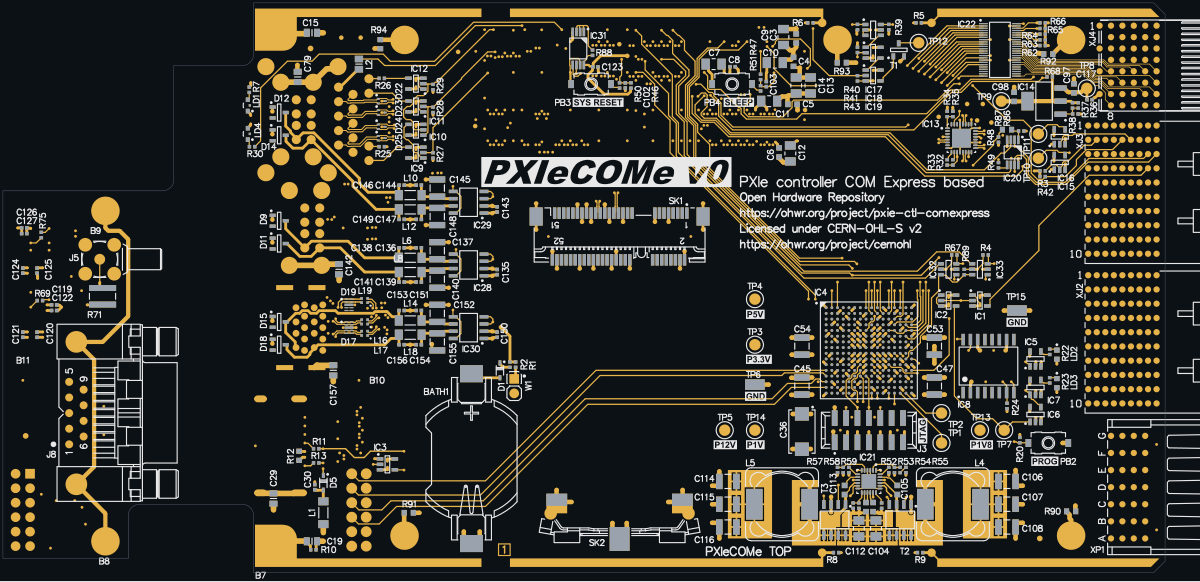
PXIE CTL COMEXPRESS (OHWR0046 R1) is an open-hardware circuit board from the CERN Open Hardware Repository, designed in Altium Designer: a 8-layer board of 204 × 100 mm with 396 components and 357 nets, published under CERN-OHL-S-2.0.
review 75% walked · 16 findings: 2 blocker · 8 major · 6 minor (92 items)
Open in the interactive viewerRead the full review
Design review
Probe recorded 16 findings: 2 blocker · 8 major · 6 minor (92 items) on this design. Each is shown here with its reasoning; the full review links every one to the pins, nets and datasheet pages it rests on.
- NetCopperSplitblockerOpen
NetCopperSplit: 4 boards×4
Refuted once, awaiting a second check · Claude walker W2 (Cern session)
At split:GND, split:GNDM, split:P3V3, split:P5V
Each finding, with its own headline
split:GNDGND's copper is in 3 pieces: C16.1 and 1 other piece(s) are not connected to the rest of the net
GND's copper is in 3 pieces: C16.1 and 1 other piece(s) are not connected to the rest of the net. Piece 1: BATH1.2, C1.1, C10.1, C100.1, C101.1, C102.1, C103.1, C104.1 and 462 more pin(s), on L1_TOP_LAYER, L3, L6 and L8_BOTTOM_LAYER, 440 drill(s), 38.42 mm2 of pour, over (-1.35, 3.19) to (157.05, 96.81). Piece 2: C16.1, on L8_BOTTOM_LAYER, over (147.3, 5.38) to (151.05, 6.83). Piece 3: C17.1, on L8_BOTTOM_LAYER, over (147.3, 13.93) to (151.05, 15.55). The export files every one of these pins under the net, so every connectivity check passes; the copper the fab builds leaves them apart. Usually a pour island that touches only one via of its own net, or a track ending short of its copper: join the piece to the net and export again.
split:GNDMGNDM's copper is in 2 pieces: D21.2 is not connected to the rest of the net
GNDM's copper is in 2 pieces: D21.2 is not connected to the rest of the net. Piece 1: C119.1, C120.1, C121.1, C122.1, C124.1, C125.1, C126.1, C127.1 and 28 more pin(s), on L1_TOP_LAYER, L3, L6 and L8_BOTTOM_LAYER, 27 drill(s), over (-42.62, 3.44) to (-23.26, 60.81). Piece 2: D21.2, on L8_BOTTOM_LAYER, over (-27.35, 56.34) to (-23.26, 58.74). The export files every one of these pins under the net, so every connectivity check passes; the copper the fab builds leaves them apart. Usually a pour island that touches only one via of its own net, or a track ending short of its copper: join the piece to the net and export again.
split:P3V3P3V3's copper is in 2 pieces: C16.2 is not connected to the rest of the net
P3V3's copper is in 2 pieces: C16.2 is not connected to the rest of the net. Piece 1: C1.2, C118.2, C159.2, C160.2, C161.2, C2.2, C28.2, C31.2 and 114 more pin(s), on L1_TOP_LAYER, L3, L6 and L8_BOTTOM_LAYER, 70 drill(s), over (-1.35, 6.5) to (157.05, 96.81). Piece 2: C16.2, on L8_BOTTOM_LAYER, over (147.3, 8.18) to (151.05, 9.63). The export files every one of these pins under the net, so every connectivity check passes; the copper the fab builds leaves them apart. Usually a pour island that touches only one via of its own net, or a track ending short of its copper: join the piece to the net and export again.
split:P5VP5V's copper is in 2 pieces: C17.2 is not connected to the rest of the net
P5V's copper is in 2 pieces: C17.2 is not connected to the rest of the net. Piece 1: C135.2, C143.2, C150.2, IC28.2, IC28.3, IC28.4, IC29.2, IC29.3 and 5 more pin(s), on L1_TOP_LAYER, L3, L6 and L8_BOTTOM_LAYER, 8 drill(s), over (18.82, 11.45) to (157.05, 67.21). Piece 2: C17.2, on L8_BOTTOM_LAYER, over (147.3, 11.13) to (151.05, 12.58). The export files every one of these pins under the net, so every connectivity check passes; the copper the fab builds leaves them apart. Usually a pour island that touches only one via of its own net, or a track ending short of its copper: join the piece to the net and export again.
- NetCopperSplitblockerOpen
SHIELD's copper is in 5 pieces: C79.2 and J4.SHIELD and 3 other piece(s) are not connected to the rest of the net
SHIELD's copper is in 5 pieces: C79.2 and J4.SHIELD and 3 other piece(s) are not connected to the rest of the net. Piece 1: B6.1, B7.1, C15.1, C19.1, J10.19, J10.20, J2.SHIELD, J9.1 and 4 more pin(s), on L1_TOP_LAYER, L3, L6 and L8_BOTTOM_LAYER, 8 drill(s), 406.78 mm2 of pour, over (0.07, 1) to (116.82, 99). Piece 2: C79.2 and J4.SHIELD, on L1_TOP_LAYER, L3, L6 and L8_BOTTOM_LAYER, 1 drill(s), over (3.28, 84.57) to (16.32, 90.31). Piece 3: C29.2, on L1_TOP_LAYER, over (0.07, 13.38) to (9.4, 14.6). Piece 4: C142.2, on L1_TOP_LAYER, over (4.78, 52.43) to (15.7, 55.43). Piece 5: C157.2, on L1_TOP_LAYER, over (9.63, 34.03) to (14.7, 38.83). The export files every one of these pins under the net, so every connectivity check passes; the copper the fab builds leaves them apart. Usually a pour island that touches only one via of its own net, or a track ending short of its copper: join the piece to the net and export again.
At split:SHIELD
IC22 bus switch crosses PXI_TRIG0 and PXI_TRIG1: the schematic symbol swaps the pin numbers of 2A3 and 2A4
The IC22 bus switch crosses PXI_TRIG0 and PXI_TRIG1 to the backplane, because the schematic symbol swaps the pin numbers of 2A3 and 2A4.
IC22 (SN74CB3T16210DGVR) couples the FPGA-side PXI trigger lines to the backplane connector XJ4 (schematic sheet 10 'PXI Express XJ4').
The pin mismatch
Channel Symbol on sheet 10 TI DGV pinout Source 2A3 pin 18 (net PXI_TRIG1) pin 16 SN74CB3T16210 datasheet, p.1 2A4 pin 16 (net PXI_TRIG0) pin 18 SN74CB3T16210 datasheet, p.1 2B3 pin 33 (C_PXI_TRIG1) pin 33 SN74CB3T16210 datasheet, p.1 2B4 pin 31 (C_PXI_TRIG0) pin 31 SN74CB3T16210 datasheet, p.1 As built
``
mermaid flowchart LR A["FPGA IC4 ball D16<br/>net PXI_TRIG0"] -- "pin 16 = 2A3" --> S1["IC22 2A3 to 2B3"] S1 -- "pin 33, C_PXI_TRIG1" --> X1["XJ4 a7<br/>PXI_TRIG1"] B["FPGA IC4 ball D15<br/>net PXI_TRIG1"] -- "pin 18 = 2A4" --> S2["IC22 2A4 to 2B4"] S2 -- "pin 31, C_PXI_TRIG0" --> X2["XJ4 b7<br/>PXI_TRIG0"]``The other 18 channels pair correctly (1A1-1A10 to 1B1-1B10, and 2A1, 2A2, 2A5, 2A10 to their B pins, with matching net names).
Why it matters
Gateware written against the schematic net names will drive and receive PXI trigger 0 on backplane trigger line 1 and vice versa, so inter-module triggering on those two lines goes to the wrong line.
Fix: correct the IC22 symbol (2A3 = pin 16, 2A4 = pin 18) and re-route, or swap the two FPGA pin constraints and document it.
The XJ4 contact assignment itself (b7 PXI_TRIG0, a7 PXI_TRIG1) was taken from the connector symbol; the PXIe hardware specification that settles it is not on file.
- DecapOrdermajorOpen
DecapOrder: 3 findings (2 components, 1 pin)×3
3 checked by the review by Claude walker W4 (Cern session) — 2 different reasons
At IC4, IC4.K9
Each finding, with its own headline
IC4IC4 supply pins G8, J10 on 'P1V8': the smallest capacitor C51 sits 3.1 mm away, behind C48 at 0.9 mm
IC4 supply pins G8, J10 on 'P1V8': the smallest capacitor C51 sits 3.1 mm away, behind C48 at 0.9 mm. IC4.G8: the smallest value, C51 (470 nF), is 3.1 mm from the pin and C48 (4.7 uF) 0.9 mm: the high-frequency part sits behind more inductance than the bulk part, which needs it least. IC4.J10: the smallest value, C50 (470 nF), is 2.5 mm from the pin and C49 (4.7 uF) 0.5 mm: the high-frequency part sits behind more inductance than the bulk part, which needs it least. Swap them, or bring the smallest value to the pin: it serves the fastest current and is the one the loop inductance defeats. Distances are pad centre to pin centre in the board plane. The 5 mm radius, the 10x value step and the 1 mm / 1.5x tie tolerance are Probe's starting values.
IC4IC4 supply pins A16, H15, R14, T1 on 'P3V3': the smallest capacitor C64 sits 3.4 mm away, behind C61 at 0.7 mm
IC4 supply pins A16, H15, R14, T1 on 'P3V3': the smallest capacitor C64 sits 3.4 mm away, behind C61 at 0.7 mm. IC4.A16: the smallest value, C64 (470 nF), is 3.4 mm from the pin and C61 (4.7 uF) 0.7 mm: the high-frequency part sits behind more inductance than the bulk part, which needs it least. IC4.H15: the smallest value, C63 (470 nF), is 3.6 mm from the pin and C62 (4.7 uF) 1.3 mm: the high-frequency part sits behind more inductance than the bulk part, which needs it least. IC4.R14: the smallest value, C58 (470 nF), is 3.0 mm from the pin and C56 (4.7 uF) 1.5 mm: the high-frequency part sits behind more inductance than the bulk part, which needs it least. IC4.T1: the smallest value, C70 (470 nF), is 3.1 mm from the pin and C67 (4.7 uF) 0.7 mm: the high-frequency part sits behind more inductance than the bulk part, which needs it least. Swap them, or bring the smallest value to the pin: it serves the fastest current and is the one the loop inductance defeats. Distances are pad centre to pin centre in the board plane. The 5 mm radius, the 10x value step and the 1 mm / 1.5x tie tolerance are Probe's starting values.
IC4.K9IC4 supply pin K9 on 'P1V': the smallest capacitor C46 sits 2.5 mm away, behind C38 at 1.2 mm
IC4 supply pin K9 on 'P1V': the smallest capacitor C46 sits 2.5 mm away, behind C38 at 1.2 mm. IC4.K9: the smallest value, C46 (470 nF), is 2.5 mm from the pin and C38 (4.7 uF) 1.2 mm: the high-frequency part sits behind more inductance than the bulk part, which needs it least. Swap them, or bring the smallest value to the pin: it serves the fastest current and is the one the loop inductance defeats. Distances are pad centre to pin centre in the board plane. The 5 mm radius, the 10x value step and the 1 mm / 1.5x tie tolerance are Probe's starting values.
- EsdProtectorPlacementmajorOpen
EsdProtectorPlacement: 25 components×25
25 checked by the review by Claude walker W4 (Cern session) — 5 different reasons
At D13, D16, D17, D19, D21
Each finding, with its own headline
D13D13.1 on 'D5_P': D13 joins the line 17.45 mm from J4.7 on a 19.37 mm run to L13.2
D13 (RCLAMP0524PA) protects 'D5_P' at J4.7. Along the copper: 17.45 mm of track from the contact, 0 via(s) before it, the line runs through its pad (flow-through); the line runs 19.37 mm on to L13.2; D13 sits 4.41 mm farther from the contact than the nearest place outside J4.
D13 joins the line 17.45 mm from J4.7 on a 19.37 mm run to L13.2: nearer the far end than the contact, so the surge travels most of the line before it is clamped.
Measured on the copper the ODB states: tracks, the pads they land on, and the netlist's vias. Not a straight line between centroids.
D13D13.10 on 'D5_P': D13 joins the line 16.57 mm from J4.7 on a 19.37 mm run to L13.2
D13 (RCLAMP0524PA) protects 'D5_P' at J4.7. Along the copper: 16.57 mm of track from the contact, 0 via(s) before it, the line runs through its pad (flow-through); the line runs 19.37 mm on to L13.2; D13 sits 4.41 mm farther from the contact than the nearest place outside J4.
D13 joins the line 16.57 mm from J4.7 on a 19.37 mm run to L13.2: nearer the far end than the contact, so the surge travels most of the line before it is clamped.
Measured on the copper the ODB states: tracks, the pads they land on, and the netlist's vias. Not a straight line between centroids.
D13D13.2 on 'D5_N': D13 joins the line 17.45 mm from J4.6 on a 19.37 mm run to L13.3
D13 (RCLAMP0524PA) protects 'D5_N' at J4.6. Along the copper: 17.45 mm of track from the contact, 0 via(s) before it, the line runs through its pad (flow-through); the line runs 19.37 mm on to L13.3; D13 sits 2.85 mm farther from the contact than the nearest place outside J4.
D13 joins the line 17.45 mm from J4.6 on a 19.37 mm run to L13.3: nearer the far end than the contact, so the surge travels most of the line before it is clamped.
Measured on the copper the ODB states: tracks, the pads they land on, and the netlist's vias. Not a straight line between centroids.
D13D13.4 on 'D4_P': 1 via(s) between J4.3 and D13.4
D13 (RCLAMP0524PA) protects 'D4_P' at J4.3. Along the copper: 21.55 mm of track from the contact, 1 via(s) before it, the line runs through its pad (flow-through); the line runs 23.46 mm on to L11.2; D13 sits 6.09 mm farther from the contact than the nearest place outside J4.
1 via(s) between J4.3 and D13.4: the strike reaches an inner layer before it is clamped. D13 joins the line 21.55 mm from J4.3 on a 23.46 mm run to L11.2: nearer the far end than the contact, so the surge travels most of the line before it is clamped.
Measured on the copper the ODB states: tracks, the pads they land on, and the netlist's vias. Not a straight line between centroids.
D13D13.5 on 'D4_N': 1 via(s) between J4.2 and D13.5
D13 (RCLAMP0524PA) protects 'D4_N' at J4.2. Along the copper: 21.73 mm of track from the contact, 1 via(s) before it, the line runs through its pad (flow-through); the line runs 23.66 mm on to L11.3; D13 sits 4.71 mm farther from the contact than the nearest place outside J4.
1 via(s) between J4.2 and D13.5: the strike reaches an inner layer before it is clamped. D13 joins the line 21.73 mm from J4.2 on a 23.66 mm run to L11.3: nearer the far end than the contact, so the surge travels most of the line before it is clamped.
Measured on the copper the ODB states: tracks, the pads they land on, and the netlist's vias. Not a straight line between centroids.
D13D13.6 on 'D4_N': 1 via(s) between J4.2 and D13.6
D13 (RCLAMP0524PA) protects 'D4_N' at J4.2. Along the copper: 20.85 mm of track from the contact, 1 via(s) before it, the line runs through its pad (flow-through); the line runs 23.66 mm on to L11.3; D13 sits 4.71 mm farther from the contact than the nearest place outside J4.
1 via(s) between J4.2 and D13.6: the strike reaches an inner layer before it is clamped. D13 joins the line 20.85 mm from J4.2 on a 23.66 mm run to L11.3: nearer the far end than the contact, so the surge travels most of the line before it is clamped.
Measured on the copper the ODB states: tracks, the pads they land on, and the netlist's vias. Not a straight line between centroids.
D13D13.7 on 'D4_P': 1 via(s) between J4.3 and D13.7
D13 (RCLAMP0524PA) protects 'D4_P' at J4.3. Along the copper: 20.67 mm of track from the contact, 1 via(s) before it, the line runs through its pad (flow-through); the line runs 23.46 mm on to L11.2; D13 sits 6.09 mm farther from the contact than the nearest place outside J4.
1 via(s) between J4.3 and D13.7: the strike reaches an inner layer before it is clamped. D13 joins the line 20.67 mm from J4.3 on a 23.46 mm run to L11.2: nearer the far end than the contact, so the surge travels most of the line before it is clamped.
Measured on the copper the ODB states: tracks, the pads they land on, and the netlist's vias. Not a straight line between centroids.
D13D13.9 on 'D5_N': D13 joins the line 16.58 mm from J4.6 on a 19.37 mm run to L13.3
D13 (RCLAMP0524PA) protects 'D5_N' at J4.6. Along the copper: 16.58 mm of track from the contact, 0 via(s) before it, the line runs through its pad (flow-through); the line runs 19.37 mm on to L13.3; D13 sits 2.85 mm farther from the contact than the nearest place outside J4.
D13 joins the line 16.58 mm from J4.6 on a 19.37 mm run to L13.3: nearer the far end than the contact, so the surge travels most of the line before it is clamped.
Measured on the copper the ODB states: tracks, the pads they land on, and the netlist's vias. Not a straight line between centroids.
D16D16.1 on 'D0_P': 1 via(s) between J10.3 and D16.1
D16 (RCLAMP0524PA) protects 'D0_P' at J10.3. Along the copper: 17.53 mm of track from the contact, 1 via(s) before it, the line runs through its pad (flow-through); the line runs 19.34 mm on to L15.2; D16 sits 7.38 mm farther from the contact than the nearest place outside J10.
1 via(s) between J10.3 and D16.1: the strike reaches an inner layer before it is clamped. D16 joins the line 17.53 mm from J10.3 on a 19.34 mm run to L15.2: nearer the far end than the contact, so the surge travels most of the line before it is clamped.
Measured on the copper the ODB states: tracks, the pads they land on, and the netlist's vias. Not a straight line between centroids.
D16D16.10 on 'D0_P': 1 via(s) between J10.3 and D16.10
D16 (RCLAMP0524PA) protects 'D0_P' at J10.3. Along the copper: 16.65 mm of track from the contact, 1 via(s) before it, the line runs through its pad (flow-through); the line runs 19.34 mm on to L15.2; D16 sits 7.38 mm farther from the contact than the nearest place outside J10.
1 via(s) between J10.3 and D16.10: the strike reaches an inner layer before it is clamped. D16 joins the line 16.65 mm from J10.3 on a 19.34 mm run to L15.2: nearer the far end than the contact, so the surge travels most of the line before it is clamped.
Measured on the copper the ODB states: tracks, the pads they land on, and the netlist's vias. Not a straight line between centroids.
D16D16.2 on 'D0_N': 1 via(s) between J10.2 and D16.2
D16 (RCLAMP0524PA) protects 'D0_N' at J10.2. Along the copper: 17.45 mm of track from the contact, 1 via(s) before it, the line runs through its pad (flow-through); the line runs 19.27 mm on to L15.3; D16 sits 7.99 mm farther from the contact than the nearest place outside J10.
1 via(s) between J10.2 and D16.2: the strike reaches an inner layer before it is clamped. D16 joins the line 17.45 mm from J10.2 on a 19.27 mm run to L15.3: nearer the far end than the contact, so the surge travels most of the line before it is clamped.
Measured on the copper the ODB states: tracks, the pads they land on, and the netlist's vias. Not a straight line between centroids.
D16D16.9 on 'D0_N': 1 via(s) between J10.2 and D16.9
D16 (RCLAMP0524PA) protects 'D0_N' at J10.2. Along the copper: 16.58 mm of track from the contact, 1 via(s) before it, the line runs through its pad (flow-through); the line runs 19.27 mm on to L15.3; D16 sits 7.99 mm farther from the contact than the nearest place outside J10.
1 via(s) between J10.2 and D16.9: the strike reaches an inner layer before it is clamped. D16 joins the line 16.58 mm from J10.2 on a 19.27 mm run to L15.3: nearer the far end than the contact, so the surge travels most of the line before it is clamped.
Measured on the copper the ODB states: tracks, the pads they land on, and the netlist's vias. Not a straight line between centroids.
D17D17.1 on 'SSRX0_N': 1 via(s) between J10.5 and D17.1
D17 (RCLAMP0524PA) protects 'SSRX0_N' at J10.5. Along the copper: 9.7 mm of track from the contact, 1 via(s) before it, the line runs through its pad (flow-through); the line runs 12.58 mm on to L16.3; D17 sits 4.72 mm farther from the contact than the nearest place outside J10.
1 via(s) between J10.5 and D17.1: the strike reaches an inner layer before it is clamped. D17 joins the line 9.7 mm from J10.5 on a 12.58 mm run to L16.3: nearer the far end than the contact, so the surge travels most of the line before it is clamped.
Measured on the copper the ODB states: tracks, the pads they land on, and the netlist's vias. Not a straight line between centroids.
D17D17.10 on 'SSRX0_N': 1 via(s) between J10.5 and D17.10
D17 (RCLAMP0524PA) protects 'SSRX0_N' at J10.5. Along the copper: 10.6 mm of track from the contact, 1 via(s) before it, the line runs through its pad (flow-through); the line runs 12.58 mm on to L16.3; D17 sits 4.72 mm farther from the contact than the nearest place outside J10.
1 via(s) between J10.5 and D17.10: the strike reaches an inner layer before it is clamped. D17 joins the line 10.6 mm from J10.5 on a 12.58 mm run to L16.3: nearer the far end than the contact, so the surge travels most of the line before it is clamped.
Measured on the copper the ODB states: tracks, the pads they land on, and the netlist's vias. Not a straight line between centroids.
D17D17.2 on 'SSRX0_P': 1 via(s) between J10.6 and D17.2
D17 (RCLAMP0524PA) protects 'SSRX0_P' at J10.6. Along the copper: 9.57 mm of track from the contact, 1 via(s) before it, the line runs through its pad (flow-through); the line runs 12.45 mm on to L16.2; D17 sits 4.24 mm farther from the contact than the nearest place outside J10.
1 via(s) between J10.6 and D17.2: the strike reaches an inner layer before it is clamped. D17 joins the line 9.57 mm from J10.6 on a 12.45 mm run to L16.2: nearer the far end than the contact, so the surge travels most of the line before it is clamped.
Measured on the copper the ODB states: tracks, the pads they land on, and the netlist's vias. Not a straight line between centroids.
D17D17.4 on 'SSTX0_N': 1 via(s) between J10.8 and D17.4
D17 (RCLAMP0524PA) protects 'SSTX0_N' at J10.8. Along the copper: 9.57 mm of track from the contact, 1 via(s) before it, the line runs through its pad (flow-through); the line runs 12.45 mm on to L17.3; D17 sits 4.24 mm farther from the contact than the nearest place outside J10.
1 via(s) between J10.8 and D17.4: the strike reaches an inner layer before it is clamped. D17 joins the line 9.57 mm from J10.8 on a 12.45 mm run to L17.3: nearer the far end than the contact, so the surge travels most of the line before it is clamped.
Measured on the copper the ODB states: tracks, the pads they land on, and the netlist's vias. Not a straight line between centroids.
D17D17.5 on 'SSTX0_P': 1 via(s) between J10.9 and D17.5
D17 (RCLAMP0524PA) protects 'SSTX0_P' at J10.9. Along the copper: 9.7 mm of track from the contact, 1 via(s) before it, the line runs through its pad (flow-through); the line runs 12.58 mm on to L17.2; D17 sits 4.72 mm farther from the contact than the nearest place outside J10.
1 via(s) between J10.9 and D17.5: the strike reaches an inner layer before it is clamped. D17 joins the line 9.7 mm from J10.9 on a 12.58 mm run to L17.2: nearer the far end than the contact, so the surge travels most of the line before it is clamped.
Measured on the copper the ODB states: tracks, the pads they land on, and the netlist's vias. Not a straight line between centroids.
D17D17.6 on 'SSTX0_P': 1 via(s) between J10.9 and D17.6
D17 (RCLAMP0524PA) protects 'SSTX0_P' at J10.9. Along the copper: 10.6 mm of track from the contact, 1 via(s) before it, the line runs through its pad (flow-through); the line runs 12.58 mm on to L17.2; D17 sits 4.72 mm farther from the contact than the nearest place outside J10.
1 via(s) between J10.9 and D17.6: the strike reaches an inner layer before it is clamped. D17 joins the line 10.6 mm from J10.9 on a 12.58 mm run to L17.2: nearer the far end than the contact, so the surge travels most of the line before it is clamped.
Measured on the copper the ODB states: tracks, the pads they land on, and the netlist's vias. Not a straight line between centroids.
D17D17.7 on 'SSTX0_N': 1 via(s) between J10.8 and D17.7
D17 (RCLAMP0524PA) protects 'SSTX0_N' at J10.8. Along the copper: 10.47 mm of track from the contact, 1 via(s) before it, the line runs through its pad (flow-through); the line runs 12.45 mm on to L17.3; D17 sits 4.24 mm farther from the contact than the nearest place outside J10.
1 via(s) between J10.8 and D17.7: the strike reaches an inner layer before it is clamped. D17 joins the line 10.47 mm from J10.8 on a 12.45 mm run to L17.3: nearer the far end than the contact, so the surge travels most of the line before it is clamped.
Measured on the copper the ODB states: tracks, the pads they land on, and the netlist's vias. Not a straight line between centroids.
D17D17.9 on 'SSRX0_P': 1 via(s) between J10.6 and D17.9
D17 (RCLAMP0524PA) protects 'SSRX0_P' at J10.6. Along the copper: 10.47 mm of track from the contact, 1 via(s) before it, the line runs through its pad (flow-through); the line runs 12.45 mm on to L16.2; D17 sits 4.24 mm farther from the contact than the nearest place outside J10.
1 via(s) between J10.6 and D17.9: the strike reaches an inner layer before it is clamped. D17 joins the line 10.47 mm from J10.6 on a 12.45 mm run to L16.2: nearer the far end than the contact, so the surge travels most of the line before it is clamped.
Measured on the copper the ODB states: tracks, the pads they land on, and the netlist's vias. Not a straight line between centroids.
D19D19.1 on 'D1_P': 1 via(s) between J10.12 and D19.1
D19 (RCLAMP0524PA) protects 'D1_P' at J10.12. Along the copper: 9.97 mm of track from the contact, 1 via(s) before it, the line runs through its pad (flow-through); the line runs 12.66 mm on to L19.3; D19 sits at J10, within 1.08 mm of the nearest place outside it to the contact: the track to it is mostly the escape out of J10's own pins, which no placement shortens.
1 via(s) between J10.12 and D19.1: the strike reaches an inner layer before it is clamped.
Measured on the copper the ODB states: tracks, the pads they land on, and the netlist's vias. Not a straight line between centroids.
D19D19.10 on 'D1_P': 1 via(s) between J10.12 and D19.10
D19 (RCLAMP0524PA) protects 'D1_P' at J10.12. Along the copper: 10.84 mm of track from the contact, 1 via(s) before it, the line runs through its pad (flow-through); the line runs 12.66 mm on to L19.3; D19 sits at J10, within 1.08 mm of the nearest place outside it to the contact: the track to it is mostly the escape out of J10's own pins, which no placement shortens.
1 via(s) between J10.12 and D19.10: the strike reaches an inner layer before it is clamped.
Measured on the copper the ODB states: tracks, the pads they land on, and the netlist's vias. Not a straight line between centroids.
D19D19.2 on 'D1_N': 1 via(s) between J10.11 and D19.2
D19 (RCLAMP0524PA) protects 'D1_N' at J10.11. Along the copper: 9.88 mm of track from the contact, 1 via(s) before it, the line runs through its pad (flow-through); the line runs 12.58 mm on to L19.2; D19 sits 1.99 mm farther from the contact than the nearest place outside J10.
1 via(s) between J10.11 and D19.2: the strike reaches an inner layer before it is clamped. D19 joins the line 9.88 mm from J10.11 on a 12.58 mm run to L19.2: nearer the far end than the contact, so the surge travels most of the line before it is clamped.
Measured on the copper the ODB states: tracks, the pads they land on, and the netlist's vias. Not a straight line between centroids.
D19D19.9 on 'D1_N': 1 via(s) between J10.11 and D19.9
D19 (RCLAMP0524PA) protects 'D1_N' at J10.11. Along the copper: 10.76 mm of track from the contact, 1 via(s) before it, the line runs through its pad (flow-through); the line runs 12.58 mm on to L19.2; D19 sits 1.99 mm farther from the contact than the nearest place outside J10.
1 via(s) between J10.11 and D19.9: the strike reaches an inner layer before it is clamped. D19 joins the line 10.76 mm from J10.11 on a 12.58 mm run to L19.2: nearer the far end than the contact, so the surge travels most of the line before it is clamped.
Measured on the copper the ODB states: tracks, the pads they land on, and the netlist's vias. Not a straight line between centroids.
D21D21.1 on 'NetD21_1': D21.1 hangs 1.85 mm off the line (limit 1 mm, default
D21 (0402ESDA-MLP) protects 'NetD21_1' at J5.1. Along the copper: 1.85 mm of track from the contact, 0 via(s) before it, on a 1.85 mm branch off the line; the line runs 2.03 mm on to R79.1; D21 sits at J5, within 0 mm of the nearest place outside it to the contact: the track to it is mostly the escape out of J5's own pins, which no placement shortens.
D21.1 hangs 1.85 mm off the line (limit 1 mm, default: no datasheet figure on file): the line carries the strike past it while the clamp is reached through the branch.
Measured on the copper the ODB states: tracks, the pads they land on, and the netlist's vias. Not a straight line between centroids.
- EsdProtectorPlacementmajorOpen
EsdProtectorPlacement: 8 components×8
8 checked by the review by Claude walker W2 (Cern session) — 8 different reasons
At D10, D2
Each finding, with its own headline
D10D10.4 on 'D2_N': 1 via(s) between J9.B2 and D10.4
D10 (RCLAMP0524PA) protects 'D2_N' at J9.B2. Along the copper: 9.83 mm of track from the contact, 1 via(s) before it, the line runs through its pad (flow-through); the line runs 12.62 mm on to L7.3; D10 sits 5.14 mm farther from the contact than the nearest place outside J9.
1 via(s) between J9.B2 and D10.4: the strike reaches an inner layer before it is clamped. D10 joins the line 9.83 mm from J9.B2 on a 12.62 mm run to L7.3: nearer the far end than the contact, so the surge travels most of the line before it is clamped.
Measured on the copper the ODB states: tracks, the pads they land on, and the netlist's vias. Not a straight line between centroids.
D10D10.5 on 'D2_P': 1 via(s) between J9.B3 and D10.5
D10 (RCLAMP0524PA) protects 'D2_P' at J9.B3. Along the copper: 9.69 mm of track from the contact, 1 via(s) before it, the line runs through its pad (flow-through); the line runs 12.5 mm on to L7.2; D10 sits 5.14 mm farther from the contact than the nearest place outside J9.
1 via(s) between J9.B3 and D10.5: the strike reaches an inner layer before it is clamped. D10 joins the line 9.69 mm from J9.B3 on a 12.5 mm run to L7.2: nearer the far end than the contact, so the surge travels most of the line before it is clamped.
Measured on the copper the ODB states: tracks, the pads they land on, and the netlist's vias. Not a straight line between centroids.
D10D10.6 on 'D2_P': 1 via(s) between J9.B3 and D10.6
D10 (RCLAMP0524PA) protects 'D2_P' at J9.B3. Along the copper: 10.6 mm of track from the contact, 1 via(s) before it, the line runs through its pad (flow-through); the line runs 12.5 mm on to L7.2; D10 sits 5.14 mm farther from the contact than the nearest place outside J9.
1 via(s) between J9.B3 and D10.6: the strike reaches an inner layer before it is clamped. D10 joins the line 10.6 mm from J9.B3 on a 12.5 mm run to L7.2: nearer the far end than the contact, so the surge travels most of the line before it is clamped.
Measured on the copper the ODB states: tracks, the pads they land on, and the netlist's vias. Not a straight line between centroids.
D10D10.7 on 'D2_N': 1 via(s) between J9.B2 and D10.7
D10 (RCLAMP0524PA) protects 'D2_N' at J9.B2. Along the copper: 10.7 mm of track from the contact, 1 via(s) before it, the line runs through its pad (flow-through); the line runs 12.62 mm on to L7.3; D10 sits 5.14 mm farther from the contact than the nearest place outside J9.
1 via(s) between J9.B2 and D10.7: the strike reaches an inner layer before it is clamped. D10 joins the line 10.7 mm from J9.B2 on a 12.62 mm run to L7.3: nearer the far end than the contact, so the surge travels most of the line before it is clamped.
Measured on the copper the ODB states: tracks, the pads they land on, and the netlist's vias. Not a straight line between centroids.
D2D2.4 on 'C_DP_HPD': 1 via(s) between J2.18 and D2.4
D2 (RCLAMP0524PA) protects 'C_DP_HPD' at J2.18. Along the copper: 2.8 mm of track from the contact, 1 via(s) before it, on a 2.8 mm branch off the line; the line runs 0 mm on to R13.2; D2 sits at J2, within 1.18 mm of the nearest place outside it to the contact: the track to it is mostly the escape out of J2's own pins, which no placement shortens.
1 via(s) between J2.18 and D2.4: the strike reaches an inner layer before it is clamped. D2.4 hangs 2.8 mm off the line (limit 1 mm, default: no datasheet figure on file): the line carries the strike past it while the clamp is reached through the branch.
Measured on the copper the ODB states: tracks, the pads they land on, and the netlist's vias. Not a straight line between centroids.
D2D2.5 on 'C_DP_PWR': D2.5 hangs 2.07 mm off the line (limit 1 mm, default
D2 (RCLAMP0524PA) protects 'C_DP_PWR' at J2.20. Along the copper: 3.67 mm of track from the contact, 0 via(s) before it, on a 2.07 mm branch off the line; the line runs 2.82 mm on to D5.1; D2 sits at J2, within 1.18 mm of the nearest place outside it to the contact: the track to it is mostly the escape out of J2's own pins, which no placement shortens.
D2.5 hangs 2.07 mm off the line (limit 1 mm, default: no datasheet figure on file): the line carries the strike past it while the clamp is reached through the branch.
Measured on the copper the ODB states: tracks, the pads they land on, and the netlist's vias. Not a straight line between centroids.
D2D2.6 on 'C_DP_PWR': D2.6 hangs 1.2 mm off the line (limit 1 mm, default
D2 (RCLAMP0524PA) protects 'C_DP_PWR' at J2.20. Along the copper: 2.8 mm of track from the contact, 0 via(s) before it, on a 1.2 mm branch off the line; the line runs 2.82 mm on to D5.1; D2 sits at J2, within 1.18 mm of the nearest place outside it to the contact: the track to it is mostly the escape out of J2's own pins, which no placement shortens.
D2.6 hangs 1.2 mm off the line (limit 1 mm, default: no datasheet figure on file): the line carries the strike past it while the clamp is reached through the branch.
Measured on the copper the ODB states: tracks, the pads they land on, and the netlist's vias. Not a straight line between centroids.
D2D2.7 on 'C_DP_HPD': 1 via(s) between J2.18 and D2.7
D2 (RCLAMP0524PA) protects 'C_DP_HPD' at J2.18. Along the copper: 1.93 mm of track from the contact, 1 via(s) before it, on a 1.93 mm branch off the line; the line runs 0 mm on to R13.2; D2 sits at J2, within 1.18 mm of the nearest place outside it to the contact: the track to it is mostly the escape out of J2's own pins, which no placement shortens.
1 via(s) between J2.18 and D2.7: the strike reaches an inner layer before it is clamped. D2.7 hangs 1.93 mm off the line (limit 1 mm, default: no datasheet figure on file): the line carries the strike past it while the clamp is reached through the branch.
Measured on the copper the ODB states: tracks, the pads they land on, and the netlist's vias. Not a straight line between centroids.
- PartLifecyclemajorOpen
PartLifecycle: 3 part numbers×3
3 Obsolete · on 4 placements
At XJ2, XJ4, XP1
Each finding, with its own headline
XJ2973028 on 2 placements (XJ2, XJ3): the distributor catalogue reports "Obsolete" for TE Connectivity Erni's 973028
973028 on 2 placements (XJ2, XJ3): the distributor catalogue reports "Obsolete" for TE Connectivity Erni's 973028 — a sourcing/longevity risk to confirm against the MANUFACTURER before acting. This board's BOM names ERNI, and that is one line with TE Connectivity Erni: Tyco Electronics renamed itself TE Connectivity in March 2011, and TE completed its acquisition of ERNI Group AG (ERNI Electronics) in September 2021. A distributor delisting is not the same claim as the part being unavailable; check the vendor's own lifecycle/product-change notice for the status and any named successor. Re-read the source: GET /api/odb/parts/973028/providers (which provider said it, the maker and part number it matched, its own words, and when we asked). THE LAST BUY DATE HAS PASSED (2022-11-30, 1,446 day(s) ago), so this is a substitution rather than a buy. The distributor reports NONE left. No approved alternate is recorded for this position.
XJ4214443 on XJ4: the distributor catalogue reports "Obsolete" for TE Connectivity Erni's 214443
214443 on XJ4: the distributor catalogue reports "Obsolete" for TE Connectivity Erni's 214443 — a sourcing/longevity risk to confirm against the MANUFACTURER before acting. This board's BOM names ERNI, and that is one line with TE Connectivity Erni: Tyco Electronics renamed itself TE Connectivity in March 2011, and TE completed its acquisition of ERNI Group AG (ERNI Electronics) in September 2021. A distributor delisting is not the same claim as the part being unavailable; check the vendor's own lifecycle/product-change notice for the status and any named successor. Re-read the source: GET /api/odb/parts/214443/providers (which provider said it, the maker and part number it matched, its own words, and when we asked). THE LAST BUY DATE HAS PASSED (2022-11-30, 1,446 day(s) ago), so this is a substitution rather than a buy. The distributor reports NONE left. No approved alternate is recorded for this position.
XP1254020 on XP1: the distributor catalogue reports "Obsolete" for TE Connectivity Erni's 254020
254020 on XP1: the distributor catalogue reports "Obsolete" for TE Connectivity Erni's 254020 — a sourcing/longevity risk to confirm against the MANUFACTURER before acting. This board's BOM names ERNI, and that is one line with TE Connectivity Erni: Tyco Electronics renamed itself TE Connectivity in March 2011, and TE completed its acquisition of ERNI Group AG (ERNI Electronics) in September 2021. A distributor delisting is not the same claim as the part being unavailable; check the vendor's own lifecycle/product-change notice for the status and any named successor. Re-read the source: GET /api/odb/parts/254020/providers (which provider said it, the maker and part number it matched, its own words, and when we asked). THE LAST BUY DATE HAS PASSED (2022-11-30, 1,446 day(s) ago), so this is a substitution rather than a buy. The distributor reports 2 left. No approved alternate is recorded for this position.
- PartLifecyclemajorOpen
PartLifecycle: 8 part numbers×8
6 Obsolete, 2 Discontinued at DigiKey · on 11 placements
At IC13, IC14, IC23, IC27, IC28, IC30, J4, T2
Each finding, with its own headline
IC139DBL0452BKILF on IC13: the distributor catalogue reports "Obsolete" for Renesas Electronics Corporation's 9DBL0452BKILF
9DBL0452BKILF on IC13: the distributor catalogue reports "Obsolete" for Renesas Electronics Corporation's 9DBL0452BKILF — a sourcing/longevity risk to confirm against the MANUFACTURER before acting. This board's BOM names INTEGRATED DEVICE TECHNOLOGY (IDT), and that is one line with Renesas Electronics Corporation: Renesas completed its acquisitions of Intersil on 2017-02-24, Integrated Device Technology on 2019-03-29 and Dialog Semiconductor (which had acquired Adesto Technologies in 2020) on 2021-08-31. A distributor delisting is not the same claim as the part being unavailable; check the vendor's own lifecycle/product-change notice for the status and any named successor. Re-read the source: GET /api/odb/parts/9DBL0452BKILF/providers (which provider said it, the maker and part number it matched, its own words, and when we asked). THE LAST BUY DATE HAS PASSED (2022-12-15, 1,431 day(s) ago), so this is a substitution rather than a buy. The distributor reports NONE left. No approved alternate is recorded for this position.
IC14LM317EMP on IC14: the distributor catalogue reports "Obsolete" for Texas Instruments's LM317EMP
LM317EMP on IC14: the distributor catalogue reports "Obsolete" for Texas Instruments's LM317EMP — a sourcing/longevity risk to confirm against the MANUFACTURER before acting. That is the maker this board's BOM names (TEXAS INSTRUMENTS). A distributor delisting is not the same claim as the part being unavailable; check the vendor's own lifecycle/product-change notice for the status and any named successor. Re-read the source: GET /api/odb/parts/LM317EMP/providers (which provider said it, the maker and part number it matched, its own words, and when we asked). THE LAST BUY DATE HAS PASSED (2024-03-18, 972 day(s) ago), so this is a substitution rather than a buy. The distributor reports 678 left. No approved alternate is recorded for this position.
IC23SN74LVC1T45DBVTG4 on 2 placements (IC23, IC25): the distributor catalogue reports "Discontinued at DigiKey" for Texas Instruments's SN74LVC1T45DBVTG4
SN74LVC1T45DBVTG4 on 2 placements (IC23, IC25): the distributor catalogue reports "Discontinued at DigiKey" for Texas Instruments's SN74LVC1T45DBVTG4 — a sourcing/longevity risk to confirm against the MANUFACTURER before acting. That is the maker this board's BOM names (TEXAS INSTRUMENTS). A distributor delisting is not the same claim as the part being unavailable; check the vendor's own lifecycle/product-change notice for the status and any named successor. Re-read the source: GET /api/odb/parts/SN74LVC1T45DBVTG4/providers (which provider said it, the maker and part number it matched, its own words, and when we asked). No approved alternate is recorded for this position.
IC27SN65C3232EPW on IC27: the distributor catalogue reports "Obsolete" for Texas Instruments's SN65C3232EPW
SN65C3232EPW on IC27: the distributor catalogue reports "Obsolete" for Texas Instruments's SN65C3232EPW — a sourcing/longevity risk to confirm against the MANUFACTURER before acting. That is the maker this board's BOM names (TEXAS INSTRUMENTS). A distributor delisting is not the same claim as the part being unavailable; check the vendor's own lifecycle/product-change notice for the status and any named successor. Re-read the source: GET /api/odb/parts/SN65C3232EPW/providers (which provider said it, the maker and part number it matched, its own words, and when we asked). THE LAST BUY DATE HAS PASSED (2022-06-29, 1,600 day(s) ago), so this is a substitution rather than a buy. The distributor reports NONE left. No approved alternate is recorded for this position.
IC28TPS2052BD on 2 placements (IC28, IC29): the distributor catalogue reports "Obsolete" for Texas Instruments's TPS2052BD
TPS2052BD on 2 placements (IC28, IC29): the distributor catalogue reports "Obsolete" for Texas Instruments's TPS2052BD — a sourcing/longevity risk to confirm against the MANUFACTURER before acting. That is the maker this board's BOM names (TEXAS INSTRUMENTS). A distributor delisting is not the same claim as the part being unavailable; check the vendor's own lifecycle/product-change notice for the status and any named successor. Re-read the source: GET /api/odb/parts/TPS2052BD/providers (which provider said it, the maker and part number it matched, its own words, and when we asked). THE LAST BUY DATE HAS PASSED (2024-09-18, 788 day(s) ago), so this is a substitution rather than a buy. The distributor reports NONE left. No approved alternate is recorded for this position.
IC30TPS2062AD on IC30: the distributor catalogue reports "Obsolete" for Texas Instruments's TPS2062AD
TPS2062AD on IC30: the distributor catalogue reports "Obsolete" for Texas Instruments's TPS2062AD — a sourcing/longevity risk to confirm against the MANUFACTURER before acting. That is the maker this board's BOM names (TEXAS INSTRUMENTS). A distributor delisting is not the same claim as the part being unavailable; check the vendor's own lifecycle/product-change notice for the status and any named successor. Re-read the source: GET /api/odb/parts/TPS2062AD/providers (which provider said it, the maker and part number it matched, its own words, and when we asked). THE LAST BUY DATE HAS PASSED (2025-06-05, 528 day(s) ago), so this is a substitution rather than a buy. The distributor reports 10,493 left. No approved alternate is recorded for this position.
J4JW0-0006NL on J4: the distributor catalogue reports "Obsolete" for Pulse Electronics's JW0-0006NL
JW0-0006NL on J4: the distributor catalogue reports "Obsolete" for Pulse Electronics's JW0-0006NL — a sourcing/longevity risk to confirm against the MANUFACTURER before acting. That is the maker this board's BOM names (PULSE ELECTRONICS). A distributor delisting is not the same claim as the part being unavailable; check the vendor's own lifecycle/product-change notice for the status and any named successor. Re-read the source: GET /api/odb/parts/JW0-0006NL/providers (which provider said it, the maker and part number it matched, its own words, and when we asked). No approved alternate is recorded for this position.
T2IRF9910Pbf on 2 placements (T2, T3): the distributor catalogue reports "Discontinued at DigiKey" for Infineon Technologies's IRF9910PBF
IRF9910Pbf on 2 placements (T2, T3): the distributor catalogue reports "Discontinued at DigiKey" for Infineon Technologies's IRF9910PBF — a sourcing/longevity risk to confirm against the MANUFACTURER before acting. This board's BOM names INTERNATIONAL RECTIFIER, and that is one line with Infineon Technologies: Infineon completed its acquisitions of International Rectifier on 2015-01-13 and Cypress Semiconductor on 2020-04-16. A distributor delisting is not the same claim as the part being unavailable; check the vendor's own lifecycle/product-change notice for the status and any named successor. Re-read the source: GET /api/odb/parts/IRF9910Pbf/providers (which provider said it, the maker and part number it matched, its own words, and when we asked). No approved alternate is recorded for this position.
- ReferencePlaneDiscontinuitymajorOpen
ReferencePlaneDiscontinuity: 12 boards×12
e.g. “2 nets cross one void in the GND plane on L2 at 3 places, the longest 0.71 mm (fastest: PE3_REFCLK_N at 1 ns 10-90 %, suggested by its name)” · 9 different statements
At void:GND@L2:hole 145.45,70.51|145.76,71.43, void:GND@L2:hole 146.04,71.71|146.96,72.02, void:GND@L2:hole 146.04,72.42|146.96,72.73, void:GND@L2:hole 146.04,74.21|146.96,74.52, void:GND@L2:hole 146.04,74.92|146.96,75.23, void:GND@L2:hole 146.04,76.71|146.96,77.02 and 6 more
Each finding, with its own headline
void:GND@L2:hole 145.45,70.51|145.76,71.432 nets cross one void in the GND plane on L2 at 2 places, the longest 0.43 mm (fastest: PE1_REFCLK_N at 1 ns 10-90 %, suggested by its name)
Along 'PE_SMB_DAT' on L1_TOP_LAYER, the GND plane on L2 has 0.43 mm under the track with no copper, at (145.6, 71.18), the same plane on both sides. No single drill's anti-pad and no landing explains it: a clearance is excused only when it holds a drill and is drawn round it, or the track ends in it on the net's own pad or via, or runs through its own via's clearance and no farther. The return current detours round the void. 2 places on 2 net(s) cross it, listed below, the longest first. What cleared it: the hole at x 145.45..145.76, y 70.51..71.43. One decision covers the void: whether these tracks may cross it, or the plane should be filled under them. 1 of the 2 crossing(s) have a plane on the track's other side at most twice as far away as the broken one (to first order each plane beside a stripline carries a share of the return inversely proportional to its distance from the track). The rest leave most or all of the return to the break, so the finding is a warning.
- 'PE_SMB_DAT' on L1_TOP_LAYER at (145.6, 71.18), 0.43 mm over no copper; other side: none: the signal layer is outermost
- 'PE1_REFCLK_N' on L3 at (145.61, 71.21), 0.42 mm over no copper; other side: P5V on L4, 0.2 mm from the track against 0.18 mm to L2: 53% of the return on L2
Every site is a row of this finding's evidence, keyed by net, layers and position. GET /api/odb/boards/47/reference-planes?group=void%3AGND%40L2%3Ahole%20145.45%2C70.51%7C145.76%2C71.43 serves each with its own layer_image region; all of them lie in x 144.45..146.76, y 70.03..72.35 mm (board frame, Y up).
Read from the copper as drawn on the reference layer, along each track's centreline at exact breakpoints. The reference is the copper beside the track, never the layer's type or name. Whether it matters depends on each signal's edge rate, which nothing on file states for these nets: a slow static line crosses a split harmlessly, a fast edge does not.
void:GND@L2:hole 146.04,71.71|146.96,72.022 nets cross one void in the GND plane on L2 at 2 places, the longest 0.71 mm (fastest: PE1_REFCLK_P at 1 ns 10-90 %, suggested by its name)
Along 'PE1_REFCLK_P' on L3, the GND plane on L2 has 0.71 mm under the track with no copper, at (146.5, 71.96), the same plane on both sides. No single drill's anti-pad and no landing explains it: a clearance is excused only when it holds a drill and is drawn round it, or the track ends in it on the net's own pad or via, or runs through its own via's clearance and no farther. The return current detours round the void. 2 places on 2 net(s) cross it, listed below, the longest first. What cleared it: the hole at x 146.04..146.96, y 71.71..72.02. One decision covers the void: whether these tracks may cross it, or the plane should be filled under them. 1 of the 2 crossing(s) have a plane on the track's other side at most twice as far away as the broken one (to first order each plane beside a stripline carries a share of the return inversely proportional to its distance from the track). The rest leave most or all of the return to the break, so the finding is a warning.
- 'PE_SMB_DAT' on L1_TOP_LAYER at (146.29, 71.87), 0.43 mm over no copper; other side: none: the signal layer is outermost
- 'PE1_REFCLK_P' on L3 at (146.5, 71.96), 0.71 mm over no copper; other side: P5V on L4, 0.2 mm from the track against 0.18 mm to L2: 53% of the return on L2
Every site is a row of this finding's evidence, keyed by net, layers and position. GET /api/odb/boards/47/reference-planes?group=void%3AGND%40L2%3Ahole%20146.04%2C71.71%7C146.96%2C72.02 serves each with its own layer_image region; all of them lie in x 145.13..147.85, y 70.71..73.02 mm (board frame, Y up).
Read from the copper as drawn on the reference layer, along each track's centreline at exact breakpoints. The reference is the copper beside the track, never the layer's type or name. Whether it matters depends on each signal's edge rate, which nothing on file states for these nets: a slow static line crosses a split harmlessly, a fast edge does not.
void:GND@L2:hole 146.04,72.42|146.96,72.732 nets cross one void in the GND plane on L2 at 3 places, the longest 0.71 mm (fastest: PE3_REFCLK_N at 1 ns 10-90 %, suggested by its name)
Along 'PE3_REFCLK_N' on L3, the GND plane on L2 has 0.71 mm under the track with no copper, at (146.5, 72.48), the same plane on both sides. No single drill's anti-pad and no landing explains it: a clearance is excused only when it holds a drill and is drawn round it, or the track ends in it on the net's own pad or via, or runs through its own via's clearance and no farther. The return current detours round the void. 3 places on 2 net(s) cross it, listed below, the longest first. What cleared it: the hole at x 146.04..146.96, y 72.42..72.73. One decision covers the void: whether these tracks may cross it, or the plane should be filled under them. 1 of the 3 crossing(s) have a plane on the track's other side at most twice as far away as the broken one (to first order each plane beside a stripline carries a share of the return inversely proportional to its distance from the track). The rest leave most or all of the return to the break, so the finding is a warning.
- 'PE_SMB_CLK' on L1_TOP_LAYER at (146.49, 72.55), 0.35 mm over no copper; other side: none: the signal layer is outermost
- 'PE_SMB_CLK' on L1_TOP_LAYER at (146.79, 72.69), 0.28 mm over no copper; other side: none: the signal layer is outermost
- 'PE3_REFCLK_N' on L3 at (146.5, 72.48), 0.71 mm over no copper; other side: P5V on L4, 0.2 mm from the track against 0.18 mm to L2: 53% of the return on L2
Every site is a row of this finding's evidence, keyed by net, layers and position. GET /api/odb/boards/47/reference-planes?group=void%3AGND%40L2%3Ahole%20146.04%2C72.42%7C146.96%2C72.73 serves each with its own layer_image region; all of them lie in x 145.14..147.93, y 71.43..73.69 mm (board frame, Y up).
Read from the copper as drawn on the reference layer, along each track's centreline at exact breakpoints. The reference is the copper beside the track, never the layer's type or name. Whether it matters depends on each signal's edge rate, which nothing on file states for these nets: a slow static line crosses a split harmlessly, a fast edge does not.
void:GND@L2:hole 146.04,74.21|146.96,74.522 nets cross one void in the GND plane on L2 at 3 places, the longest 0.71 mm (fastest: PE2_REFCLK_P at 1 ns 10-90 %, suggested by its name)
Along 'PE2_REFCLK_P' on L3, the GND plane on L2 has 0.71 mm under the track with no copper, at (146.5, 74.46), the same plane on both sides. No single drill's anti-pad and no landing explains it: a clearance is excused only when it holds a drill and is drawn round it, or the track ends in it on the net's own pad or via, or runs through its own via's clearance and no farther. The return current detours round the void. 3 places on 2 net(s) cross it, listed below, the longest first. What cleared it: the hole at x 146.04..146.96, y 74.21..74.52. One decision covers the void: whether these tracks may cross it, or the plane should be filled under them. 1 of the 3 crossing(s) have a plane on the track's other side at most twice as far away as the broken one (to first order each plane beside a stripline carries a share of the return inversely proportional to its distance from the track). The rest leave most or all of the return to the break, so the finding is a warning.
- 'PE_PS_ON_N' on L1_TOP_LAYER at (146.79, 74.26), 0.28 mm over no copper; other side: none: the signal layer is outermost
- 'PE_PS_ON_N' on L1_TOP_LAYER at (146.26, 74.26), 0.23 mm over no copper; other side: none: the signal layer is outermost
- 'PE2_REFCLK_P' on L3 at (146.5, 74.46), 0.71 mm over no copper; other side: P5V on L4, 0.2 mm from the track against 0.18 mm to L2: 53% of the return on L2
Every site is a row of this finding's evidence, keyed by net, layers and position. GET /api/odb/boards/47/reference-planes?group=void%3AGND%40L2%3Ahole%20146.04%2C74.21%7C146.96%2C74.52 serves each with its own layer_image region; all of them lie in x 145.13..147.93, y 73.21..75.46 mm (board frame, Y up).
Read from the copper as drawn on the reference layer, along each track's centreline at exact breakpoints. The reference is the copper beside the track, never the layer's type or name. Whether it matters depends on each signal's edge rate, which nothing on file states for these nets: a slow static line crosses a split harmlessly, a fast edge does not.
void:GND@L2:hole 146.04,74.92|146.96,75.232 nets cross one void in the GND plane on L2 at 2 places, the longest 0.8 mm (fastest: PE_PWRBTN_N at 100 ps 10-90 %, ASSUMED)
Along 'PE_PWRBTN_N' on L1_TOP_LAYER, the GND plane on L2 has 0.8 mm under the track with no copper, at (146.5, 75), the same plane on both sides. No single drill's anti-pad and no landing explains it: a clearance is excused only when it holds a drill and is drawn round it, or the track ends in it on the net's own pad or via, or runs through its own via's clearance and no farther. The return current detours round the void. 2 places on 2 net(s) cross it, listed below, the longest first. What cleared it: the hole at x 146.04..146.96, y 74.92..75.23. One decision covers the void: whether these tracks may cross it, or the plane should be filled under them. 1 of the 2 crossing(s) have a plane on the track's other side at most twice as far away as the broken one (to first order each plane beside a stripline carries a share of the return inversely proportional to its distance from the track). The rest leave most or all of the return to the break, so the finding is a warning.
- 'PE_PWRBTN_N' on L1_TOP_LAYER at (146.5, 75), 0.8 mm over no copper; other side: none: the signal layer is outermost
- 'PE4_REFCLK_N' on L3 at (146.5, 74.98), 0.66 mm over no copper; other side: P5V on L4, 0.2 mm from the track against 0.18 mm to L2: 53% of the return on L2
Every site is a row of this finding's evidence, keyed by net, layers and position. GET /api/odb/boards/47/reference-planes?group=void%3AGND%40L2%3Ahole%20146.04%2C74.92%7C146.96%2C75.23 serves each with its own layer_image region; all of them lie in x 145.1..147.9, y 73.98..76 mm (board frame, Y up).
Read from the copper as drawn on the reference layer, along each track's centreline at exact breakpoints. The reference is the copper beside the track, never the layer's type or name. Whether it matters depends on each signal's edge rate, which nothing on file states for these nets: a slow static line crosses a split harmlessly, a fast edge does not.
void:GND@L2:hole 146.04,76.71|146.96,77.02'PE_PWR_OK' crosses one void in the GND plane on L2 at 1 place, the longest 0.41 mm (fastest: PE_PWR_OK at 100 ps 10-90 %, ASSUMED)
Along 'PE_PWR_OK' on L1_TOP_LAYER, the GND plane on L2 has 0.41 mm under the track with no copper, at (146.5, 77), the same plane on both sides. No single drill's anti-pad and no landing explains it: a clearance is excused only when it holds a drill and is drawn round it, or the track ends in it on the net's own pad or via, or runs through its own via's clearance and no farther. The return current detours round the void. What cleared it: the hole at x 146.04..146.96, y 76.71..77.02. One decision covers the void: whether these tracks may cross it, or the plane should be filled under them. No crossing has a plane on the track's other side, so the whole return meets the break.
- 'PE_PWR_OK' on L1_TOP_LAYER at (146.5, 77), 0.41 mm over no copper; other side: none: the signal layer is outermost
Every site is a row of this finding's evidence, keyed by net, layers and position. GET /api/odb/boards/47/reference-planes?group=void%3AGND%40L2%3Ahole%20146.04%2C76.71%7C146.96%2C77.02 serves each with its own layer_image region; all of them lie in x 145.3..147.7, y 76..78 mm (board frame, Y up).
Read from the copper as drawn on the reference layer, along each track's centreline at exact breakpoints. The reference is the copper beside the track, never the layer's type or name. Whether it matters depends on each signal's edge rate, which nothing on file states for these nets: a slow static line crosses a split harmlessly, a fast edge does not.
void:GND@L2:hole 150.54,72.42|151.46,72.732 nets cross one void in the GND plane on L2 at 3 places, the longest 0.71 mm (fastest: PE3_REFCLK_N at 1 ns 10-90 %, suggested by its name)
Along 'PE3_REFCLK_N' on L3, the GND plane on L2 has 0.71 mm under the track with no copper, at (151, 72.48), the same plane on both sides. No single drill's anti-pad and no landing explains it: a clearance is excused only when it holds a drill and is drawn round it, or the track ends in it on the net's own pad or via, or runs through its own via's clearance and no farther. The return current detours round the void. 3 places on 2 net(s) cross it, listed below, the longest first. What cleared it: the hole at x 150.54..151.46, y 72.42..72.73. One decision covers the void: whether these tracks may cross it, or the plane should be filled under them. 1 of the 3 crossing(s) have a plane on the track's other side at most twice as far away as the broken one (to first order each plane beside a stripline carries a share of the return inversely proportional to its distance from the track). The rest leave most or all of the return to the break, so the finding is a warning.
- 'PE_SMB_CLK' on L1_TOP_LAYER at (150.71, 72.69), 0.28 mm over no copper; other side: none: the signal layer is outermost
- 'PE_SMB_CLK' on L1_TOP_LAYER at (151.29, 72.69), 0.28 mm over no copper; other side: none: the signal layer is outermost
- 'PE3_REFCLK_N' on L3 at (151, 72.48), 0.71 mm over no copper; other side: P5V on L4, 0.2 mm from the track against 0.18 mm to L2: 53% of the return on L2
Every site is a row of this finding's evidence, keyed by net, layers and position. GET /api/odb/boards/47/reference-planes?group=void%3AGND%40L2%3Ahole%20150.54%2C72.42%7C151.46%2C72.73 serves each with its own layer_image region; all of them lie in x 149.57..152.43, y 71.48..73.69 mm (board frame, Y up).
Read from the copper as drawn on the reference layer, along each track's centreline at exact breakpoints. The reference is the copper beside the track, never the layer's type or name. Whether it matters depends on each signal's edge rate, which nothing on file states for these nets: a slow static line crosses a split harmlessly, a fast edge does not.
void:GND@L2:hole 150.54,76.71|151.46,77.02'PE_PWR_OK' crosses one void in the GND plane on L2 at 1 place, the longest 0.41 mm (fastest: PE_PWR_OK at 100 ps 10-90 %, ASSUMED)
Along 'PE_PWR_OK' on L1_TOP_LAYER, the GND plane on L2 has 0.41 mm under the track with no copper, at (151, 77), the same plane on both sides. No single drill's anti-pad and no landing explains it: a clearance is excused only when it holds a drill and is drawn round it, or the track ends in it on the net's own pad or via, or runs through its own via's clearance and no farther. The return current detours round the void. What cleared it: the hole at x 150.54..151.46, y 76.71..77.02. One decision covers the void: whether these tracks may cross it, or the plane should be filled under them. No crossing has a plane on the track's other side, so the whole return meets the break.
- 'PE_PWR_OK' on L1_TOP_LAYER at (151, 77), 0.41 mm over no copper; other side: none: the signal layer is outermost
Every site is a row of this finding's evidence, keyed by net, layers and position. GET /api/odb/boards/47/reference-planes?group=void%3AGND%40L2%3Ahole%20150.54%2C76.71%7C151.46%2C77.02 serves each with its own layer_image region; all of them lie in x 149.8..152.2, y 76..78 mm (board frame, Y up).
Read from the copper as drawn on the reference layer, along each track's centreline at exact breakpoints. The reference is the copper beside the track, never the layer's type or name. Whether it matters depends on each signal's edge rate, which nothing on file states for these nets: a slow static line crosses a split harmlessly, a fast edge does not.
void:GND@L2:hole 19.09,10.92|20.45,11.31'TRIG_OE' crosses one void in the GND plane on L2 at 1 place, the longest 0.91 mm (fastest: TRIG_OE at 100 ps 10-90 %, ASSUMED)
Along 'TRIG_OE' on L1_TOP_LAYER, the GND plane on L2 has 0.91 mm under the track with no copper, at (19.77, 11), the same plane on both sides. No single drill's anti-pad and no landing explains it: a clearance is excused only when it holds a drill and is drawn round it, or the track ends in it on the net's own pad or via, or runs through its own via's clearance and no farther. The return current detours round the void. What cleared it: the hole at x 19.09..20.45, y 10.92..11.31. One decision covers the void: whether these tracks may cross it, or the plane should be filled under them. No crossing has a plane on the track's other side, so the whole return meets the break.
- 'TRIG_OE' on L1_TOP_LAYER at (19.77, 11), 0.91 mm over no copper; other side: none: the signal layer is outermost
Every site is a row of this finding's evidence, keyed by net, layers and position. GET /api/odb/boards/47/reference-planes?group=void%3AGND%40L2%3Ahole%2019.09%2C10.92%7C20.45%2C11.31 serves each with its own layer_image region; all of them lie in x 18.31..21.23, y 10..12 mm (board frame, Y up).
Read from the copper as drawn on the reference layer, along each track's centreline at exact breakpoints. The reference is the copper beside the track, never the layer's type or name. Whether it matters depends on each signal's edge rate, which nothing on file states for these nets: a slow static line crosses a split harmlessly, a fast edge does not.
void:GND@L2:hole 19.09,8.38|20.45,8.77'TRIG_IN' crosses one void in the GND plane on L2 at 1 place, the longest 1.28 mm (fastest: TRIG_IN at 100 ps 10-90 %, ASSUMED)
Along 'TRIG_IN' on L1_TOP_LAYER, the GND plane on L2 has 1.28 mm under the track with no copper, at (19.77, 8.55), the same plane on both sides. No single drill's anti-pad and no landing explains it: a clearance is excused only when it holds a drill and is drawn round it, or the track ends in it on the net's own pad or via, or runs through its own via's clearance and no farther. The return current detours round the void. What cleared it: the hole at x 19.09..20.45, y 8.38..8.77. One decision covers the void: whether these tracks may cross it, or the plane should be filled under them. No crossing has a plane on the track's other side, so the whole return meets the break.
- 'TRIG_IN' on L1_TOP_LAYER at (19.77, 8.55), 1.28 mm over no copper; other side: none: the signal layer is outermost
Every site is a row of this finding's evidence, keyed by net, layers and position. GET /api/odb/boards/47/reference-planes?group=void%3AGND%40L2%3Ahole%2019.09%2C8.38%7C20.45%2C8.77 serves each with its own layer_image region; all of them lie in x 18.13..21.41, y 7.55..9.55 mm (board frame, Y up).
Read from the copper as drawn on the reference layer, along each track's centreline at exact breakpoints. The reference is the copper beside the track, never the layer's type or name. Whether it matters depends on each signal's edge rate, which nothing on file states for these nets: a slow static line crosses a split harmlessly, a fast edge does not.
void:GND@L7:hole 145.45,73.01|145.76,73.93'PE_LINKCAP' crosses one void in the GND plane on L7 at 1 place, the longest 0.43 mm (fastest: PE_LINKCAP at 100 ps 10-90 %, ASSUMED)
Along 'PE_LINKCAP' on L8_BOTTOM_LAYER, the GND plane on L7 has 0.43 mm under the track with no copper, at (145.6, 73.68), the same plane on both sides. No single drill's anti-pad and no landing explains it: a clearance is excused only when it holds a drill and is drawn round it, or the track ends in it on the net's own pad or via, or runs through its own via's clearance and no farther. The return current detours round the void. What cleared it: the hole at x 145.45..145.76, y 73.01..73.93. One decision covers the void: whether these tracks may cross it, or the plane should be filled under them. No crossing has a plane on the track's other side, so the whole return meets the break.
- 'PE_LINKCAP' on L8_BOTTOM_LAYER at (145.6, 73.68), 0.43 mm over no copper; other side: none: the signal layer is outermost
Every site is a row of this finding's evidence, keyed by net, layers and position. GET /api/odb/boards/47/reference-planes?group=void%3AGND%40L7%3Ahole%20145.45%2C73.01%7C145.76%2C73.93 serves each with its own layer_image region; all of them lie in x 144.45..146.76, y 72.53..74.84 mm (board frame, Y up).
Read from the copper as drawn on the reference layer, along each track's centreline at exact breakpoints. The reference is the copper beside the track, never the layer's type or name. Whether it matters depends on each signal's edge rate, which nothing on file states for these nets: a slow static line crosses a split harmlessly, a fast edge does not.
void:GND@L7:hole 146.04,74.21|146.96,74.52'PE_LINKCAP' crosses one void in the GND plane on L7 at 1 place, the longest 0.43 mm (fastest: PE_LINKCAP at 100 ps 10-90 %, ASSUMED)
Along 'PE_LINKCAP' on L8_BOTTOM_LAYER, the GND plane on L7 has 0.43 mm under the track with no copper, at (146.29, 74.37), the same plane on both sides. No single drill's anti-pad and no landing explains it: a clearance is excused only when it holds a drill and is drawn round it, or the track ends in it on the net's own pad or via, or runs through its own via's clearance and no farther. The return current detours round the void. What cleared it: the hole at x 146.04..146.96, y 74.21..74.52. One decision covers the void: whether these tracks may cross it, or the plane should be filled under them. No crossing has a plane on the track's other side, so the whole return meets the break.
- 'PE_LINKCAP' on L8_BOTTOM_LAYER at (146.29, 74.37), 0.43 mm over no copper; other side: none: the signal layer is outermost
Every site is a row of this finding's evidence, keyed by net, layers and position. GET /api/odb/boards/47/reference-planes?group=void%3AGND%40L7%3Ahole%20146.04%2C74.21%7C146.96%2C74.52 serves each with its own layer_image region; all of them lie in x 145.13..147.44, y 73.21..75.52 mm (board frame, Y up).
Read from the copper as drawn on the reference layer, along each track's centreline at exact breakpoints. The reference is the copper beside the track, never the layer's type or name. Whether it matters depends on each signal's edge rate, which nothing on file states for these nets: a slow static line crosses a split harmlessly, a fast edge does not.
- PlaneEdgeStitchingmajorOpen
The GND planes on L2 and L7 are unstitched along 64.47 mm of board edge (limit 53.13 mm, lambda/20 at 143 MHz, the knee of 'PE_PS_ON_N', the board's fastest stated edge)
The GND planes on L2 and L7 are unstitched along 64.47 mm of board edge (limit 53.13 mm, lambda/20 at 143 MHz, the knee of 'PE_PS_ON_N', the board's fastest stated edge). Two planes of one ground make a cavity that every fast edge through it drives, and at the board edge the cavity radiates through each stretch its vias do not close. The wavelength is read at the knee of the board's fastest stated edge, 3500 ps 10-90 % on 'PE_PS_ON_N' (net: 3.5 ns 10-90 %, stated for this net by Claude walker W2 (Cern session): FDV301N datasheet (16bba729) p.3: turn-off fall time 3.5 ns typ (T1 drain is the only driver; rise via 10k pull-up R42 is far slower)), knee 143 MHz, in Dk 3.9 between the layers (the export's own stackup rows): lambda = 1062.64 mm. lambda/20 is the common rule for electrically small, declared as a heuristic, not a cited limit. Both planes reach the edge along 528.75 mm of it, and 440 stitching via(s) stand within the limit of it. Gaps: 64.47 mm from (-43.84, 2.5) (the planes leave the edge) to (-44, 66.81) (the planes leave the edge). Stitching vias along these stretches, at most the limit apart, close it.
At edgestitch:GND@L2|L7
USB and DisplayPort ESD arrays return to ground through a single via each
The USB and DisplayPort ESD arrays and the VBUS TVS diodes each reach ground through a single via, so at ESD edge rates that via's inductance adds directly to the clamp voltage the protected lines see.
What was measured
Measured from the ODB++ export: pad positions from the component layers, vias from the plated drill layer on net GND.
Protector Protects GND vias near the ground pad D10 RClamp0524PA (bottom) J9 one, 1.02 mm from pin 3 at (16.75, 60.50) mm, by a short trace; no bottom ground pour in the area D3, D4 RClamp0524PA DisplayPort J2 lanes one each, 1.02 mm from the GND pad D2 J2 HPD/DP_PWR one at 1.02 mm, a second 2.0 mm away D13 J4 USB one, 1.02-1.05 mm from pin 3 D16, D19 J10 USB 2.0 pairs one each, 1.02-1.05 mm from pin 3 D17/D20 (top/bottom stacked) J10 SuperSpeed two shared, at 1.02 and 1.25 mm D9, D11, D12, D14, D15, D18 VBUS one each, 0.75 mm from the ground pin; no other GND via within 3 mm The connectors J9 (A4/B4), J10 (4, 7, 13, 16), J4 (4, 8, 18) and J2 (2, 5, 8, 11, 16, 19) return on GND through their through-hole pins. So every protector reaches the connector return only through the inner GND plane, through its one via.
Contrast on the same board: D22-D25 (Ethernet MDI) have 2 to 6 GND vias within 3 mm of the ground pin, and D21 on the mezzanine connects to the J5 SMB ground pin by a direct trace.
Why it matters
A clamp only protects as well as its ground path. A single via of roughly 1 nH adds several volts per ampere-nanosecond of ESD current on top of the clamp voltage. Semtech and most ESD layout guides ask for the ground pad to be tied to the plane with multiple vias as close as possible.
PCA9513A SMBus buffer runs from 3.3 V while its backplane-side pull-ups go to 5 V
The PCA9513A SMBus buffer IC20 runs from 3.3 V while its backplane-side pull-ups R44/R45 go to 5 V, which the datasheet forbids: the pull-up voltage must equal VCC.
Where it is
``
mermaid flowchart LR A["P3V3AUX 3.3 V<br/>from LM317 IC14"] -- "pin 8 VCC" --> B["IC20 PCA9513ADP"] B -- "pin 7 PE_SMB_DAT, pin 2 PE_SMB_CLK" --> X["Backplane XJ3<br/>A3 and B3"] P["P5VAUX 5 V"] -- "R44, R45 3k3" --> X``The rules and the numbers
Quantity Value Source Bus pull-up voltage must equal the supply voltage when the rise time accelerators are in use PCA9513A datasheet, p.8 Pull-up above VCC 'the rise time accelerator will clamp the voltage to the positive supply rail' PCA9513A datasheet, p.16 Current from P5VAUX into the part (5 - 3.3) V / 3k3 = about 0.5 mA per line derived Why it matters
With a 5 V pull-up against a 3.3 V VCC, every rising edge the accelerator assists is clamped toward 3.3 V, the lines sit at an out-of-specification level on the backplane side, and current flows from P5VAUX through the 3k3 resistors into the part.
The sheet 17 note quotes PICMG EXP.0 3.14: a 3.3 kΩ pull-up to 5Vaux shall be used on SMBDAT and SMBCLK on the system board, and a buffer with 2 mA rise time accelerator capability is required. The side reversal (SCLIN/SDAIN on the COM Express side) is documented there as deliberate.
That requirement is consistent with running the buffer from 5 V aux; the COM Express side would then need its levels checked, since the module's SMBus is 3.3 V. Either way the present combination is outside what the part promises.
Three silkscreen designators are printed over solderable pads (L6, J7, IC27)
Three silkscreen designators ("L8", "IC27", "R72") are printed over solderable pads of L6, J7 and IC27.
Designator text Printed over Net Layer view "L8" left pad of L6, pin 2, at (25.5, 55.25) mm VBUS2 TOP_OVERLAY + TOP_SOLDER, region 22-30 x 52-60 mm "IC27" (its "7") through-hole pad of J7 pin 11, at (-39.2, 4.65) mm F_SER_RX BOTTOM_OVERLAY + BOTTOM_SOLDER, region -42..-32 x 2..14 mm "R72" upper pin row of IC27 (SN65C3232E, TSSOP-16), pins 9 and 10, at about (-35.3/-34.6, 11.45) mm no-connect and GNDM same view Found by rendering the overlay and solder-mask layers of the ODB++ export at about 30 px/mm. A scan of all 17467 overlay segments against the solder-mask openings found no other component pad under silkscreen; the other contacts are via or fiducial openings.
Why it matters
Silkscreen must stay clear of solderable copper: ink on a pad can lift a part or spoil the joint. Most fabricators clip it automatically, which avoids the solder problem but leaves the three designators partly erased, so they become ambiguous next to crowded parts.
Suggested fix: move the three texts clear of the pads.
- ConnectorDomainMixedminorOpen
ConnectorDomainMixed: 4 components×4
4 checked by the review by evaluation@esharp.se — 4 different reasons
At J1, J6, J7, XP1
Each finding, with its own headline
J1J1 takes 2 different supplies off the board on one connector: P12V (12 V), P5VAUX (5 V)
J1 carries 2 different supplies out of the board on one connector: P12V (12 V) on A104/A105/A106/A107/A108/A109/B104/B105/B106/B107/B108/B109/C104/C105/C106/C107/C108/C109/D104/D105/D106/D107/D108/D109, P5VAUX (5 V) on B84/B85/B86/B87. Declare the intent. Two rails on one connector is ordinary in a docking or power-distribution interface and a hazard in a signal one, and the difference is not visible from the netlist — but note that adjacent contacts at different voltages are exactly what a mirrored, reversed or off-by-one cable shorts together, so the cost of getting the mating wrong is a rail collision rather than a dead signal. If this is a standard connector, declare its family (connector_family_declare) and file the standard's contact map: supplies on the contacts it assigns to power are then not reported.
J6J6 takes 2 different supplies off the board on one connector: P5V (5 V), P3V3 (3.3 V)
J6 carries 2 different supplies out of the board on one connector: P5V (5 V) on 2, P3V3 (3.3 V) on 4. Declare the intent. Two rails on one connector is ordinary in a docking or power-distribution interface and a hazard in a signal one, and the difference is not visible from the netlist — but note that adjacent contacts at different voltages are exactly what a mirrored, reversed or off-by-one cable shorts together, so the cost of getting the mating wrong is a rail collision rather than a dead signal. If this is a standard connector, declare its family (connector_family_declare) and file the standard's contact map: supplies on the contacts it assigns to power are then not reported.
J7J7 takes 2 different supplies off the board on one connector: P5VM (5 V), P3V3M (3.3 V)
J7 carries 2 different supplies out of the board on one connector: P5VM (5 V) on 2, P3V3M (3.3 V) on 4. Declare the intent. Two rails on one connector is ordinary in a docking or power-distribution interface and a hazard in a signal one, and the difference is not visible from the netlist — but note that adjacent contacts at different voltages are exactly what a mirrored, reversed or off-by-one cable shorts together, so the cost of getting the mating wrong is a rail collision rather than a dead signal. If this is a standard connector, declare its family (connector_family_declare) and file the standard's contact map: supplies on the contacts it assigns to power are then not reported.
XP1XP1 takes 3 different supplies off the board on one connector: P12V (12 V), P5V (5 V), P3V3 (3.3 V)
XP1 carries 3 different supplies out of the board on one connector: P12V (12 V) on E/F, P5V (5 V) on C, P3V3 (3.3 V) on B. Declare the intent. Two rails on one connector is ordinary in a docking or power-distribution interface and a hazard in a signal one, and the difference is not visible from the netlist — but note that adjacent contacts at different voltages are exactly what a mirrored, reversed or off-by-one cable shorts together, so the cost of getting the mating wrong is a rail collision rather than a dead signal. If this is a standard connector, declare its family (connector_family_declare) and file the standard's contact map: supplies on the contacts it assigns to power are then not reported.
- DecapViaFanoutminorOpen
DecapViaFanout: 15 components×15
15 checked by the review by Claude walker W4 (Cern session) — 15 different reasons
At C10, C106, C108, C11, C116, C127 and 9 more
Each finding, with its own headline
C10C10 on 'P12V': its rail pad reaches its via over 4.19 mm of track and its ground pad over 1.70 mm, adding about 2.41 nH to its loop, past Probe's 0.5 nH starting value; put the vias at the pads (a 10 uF bulk capacitor: its inductance matters only far above the band it serves)
C10 on 'P12V': its rail pad reaches its via over 4.19 mm of track and its ground pad over 1.70 mm, adding about 2.41 nH to its loop, past Probe's 0.5 nH starting value; put the vias at the pads (a 10 uF bulk capacitor: its inductance matters only far above the band it serves). C10.2 (rail) runs 4.19 mm along its copper to its nearest via, 3.19 mm past the 1 mm beside the pad: 1.97 nH; C10.1 (ground) runs 1.70 mm along its copper to its nearest via, 0.70 mm past the 1 mm beside the pad: 0.43 nH. Each run past the pad as one conductor of a pair 2.80 mm apart (the pad pitch), 0.2 l ln(D/R) nH with R 0.127 mm (the track's width is not read): 2.41 nH in all. Put the vias at the pads (or in them), one per pad at least, the rail's and the ground's close together; the capacitor's own inductance as mounted is 1.79 nH (pad 0.20 nH + no via of the first net within 1 mm of its pad: the study's 0.6 nH per mm of 1.32 mm depth, ASSUMED). 0.5 nH is Probe's starting value, about the whole mounted inductance of a well-mounted 0402.
C106C106 on 'P1V8': its ground pad over 1.85 mm, adding about 0.54 nH to its loop, past Probe's 0.5 nH starting value; put the vias at the pads (a 47 uF bulk capacitor: its inductance matters only far above the band it serves)
C106 on 'P1V8': its ground pad over 1.85 mm, adding about 0.54 nH to its loop, past Probe's 0.5 nH starting value; put the vias at the pads (a 47 uF bulk capacitor: its inductance matters only far above the band it serves). C106.2 (rail) not measured: the pad sits in a pour of its net on its own layer, which has no track length to measure; C106.1 (ground) runs 1.85 mm along its copper to its nearest via, 0.85 mm past the 1 mm beside the pad: 0.54 nH. Each run past the pad as one conductor of a pair 3.00 mm apart (the pad pitch), 0.2 l ln(D/R) nH with R 0.127 mm (the track's width is not read): 0.54 nH in all. Put the vias at the pads (or in them), one per pad at least, the rail's and the ground's close together; the capacitor's own inductance as mounted is 1.31 nH (pad 0.20 nH + no via of the first net within 1 mm of its pad: the study's 0.6 nH per mm of 0.51 mm depth, ASSUMED). 0.5 nH is Probe's starting value, about the whole mounted inductance of a well-mounted 0402.
C108C108 on 'P1V8': its ground pad over 1.85 mm, adding about 0.54 nH to its loop, past Probe's 0.5 nH starting value; put the vias at the pads (a 100 uF bulk capacitor: its inductance matters only far above the band it serves)
C108 on 'P1V8': its ground pad over 1.85 mm, adding about 0.54 nH to its loop, past Probe's 0.5 nH starting value; put the vias at the pads (a 100 uF bulk capacitor: its inductance matters only far above the band it serves). C108.2 (rail) not measured: the pad sits in a pour of its net on its own layer, which has no track length to measure; C108.1 (ground) runs 1.85 mm along its copper to its nearest via, 0.85 mm past the 1 mm beside the pad: 0.54 nH. Each run past the pad as one conductor of a pair 3.00 mm apart (the pad pitch), 0.2 l ln(D/R) nH with R 0.127 mm (the track's width is not read): 0.54 nH in all. Put the vias at the pads (or in them), one per pad at least, the rail's and the ground's close together; the capacitor's own inductance as mounted is 1.31 nH (pad 0.20 nH + no via of the first net within 1 mm of its pad: the study's 0.6 nH per mm of 0.51 mm depth, ASSUMED). 0.5 nH is Probe's starting value, about the whole mounted inductance of a well-mounted 0402.
C11C11 on 'P12V': its rail pad reaches its via over 2.14 mm of track and its ground pad over 1.96 mm, adding about 1.30 nH to its loop, past Probe's 0.5 nH starting value; put the vias at the pads (a 10 uF bulk capacitor: its inductance matters only far above the band it serves)
C11 on 'P12V': its rail pad reaches its via over 2.14 mm of track and its ground pad over 1.96 mm, adding about 1.30 nH to its loop, past Probe's 0.5 nH starting value; put the vias at the pads (a 10 uF bulk capacitor: its inductance matters only far above the band it serves). C11.2 (rail) runs 2.14 mm along its copper to its nearest via, 1.14 mm past the 1 mm beside the pad: 0.71 nH; C11.1 (ground) runs 1.96 mm along its copper to its nearest via, 0.96 mm past the 1 mm beside the pad: 0.59 nH. Each run past the pad as one conductor of a pair 2.80 mm apart (the pad pitch), 0.2 l ln(D/R) nH with R 0.127 mm (the track's width is not read): 1.30 nH in all. Put the vias at the pads (or in them), one per pad at least, the rail's and the ground's close together; the capacitor's own inductance as mounted is 1.79 nH (pad 0.20 nH + no via of the first net within 1 mm of its pad: the study's 0.6 nH per mm of 1.32 mm depth, ASSUMED). 0.5 nH is Probe's starting value, about the whole mounted inductance of a well-mounted 0402.
C116C116 on 'P1V': its ground pad over 2.00 mm, adding about 0.63 nH to its loop, past Probe's 0.5 nH starting value; put the vias at the pads (a 100 uF bulk capacitor: its inductance matters only far above the band it serves)
C116 on 'P1V': its ground pad over 2.00 mm, adding about 0.63 nH to its loop, past Probe's 0.5 nH starting value; put the vias at the pads (a 100 uF bulk capacitor: its inductance matters only far above the band it serves). C116.2 (rail) not measured: the pad sits in a pour of its net on its own layer, which has no track length to measure; C116.1 (ground) runs 2.00 mm along its copper to its nearest via, 1.00 mm past the 1 mm beside the pad: 0.63 nH. Each run past the pad as one conductor of a pair 3.00 mm apart (the pad pitch), 0.2 l ln(D/R) nH with R 0.127 mm (the track's width is not read): 0.63 nH in all. Put the vias at the pads (or in them), one per pad at least, the rail's and the ground's close together; the capacitor's own inductance as mounted is 1.31 nH (pad 0.20 nH + no via of the first net within 1 mm of its pad: the study's 0.6 nH per mm of 0.51 mm depth, ASSUMED). 0.5 nH is Probe's starting value, about the whole mounted inductance of a well-mounted 0402.
C127C127 on 'P5VM': its rail pad reaches its via over 1.62 mm of track and its ground pad over 1.70 mm, adding about 0.52 nH to its loop, past Probe's 0.5 nH starting value; put the vias at the pads (within a quarter of the starting value)
C127 on 'P5VM': its rail pad reaches its via over 1.62 mm of track and its ground pad over 1.70 mm, adding about 0.52 nH to its loop, past Probe's 0.5 nH starting value; put the vias at the pads (within a quarter of the starting value). C127.2 (rail) runs 1.62 mm along its copper to its nearest via, 0.62 mm past the 1 mm beside the pad: 0.24 nH; C127.1 (ground) runs 1.70 mm along its copper to its nearest via, 0.70 mm past the 1 mm beside the pad: 0.27 nH. Each run past the pad as one conductor of a pair 0.90 mm apart (the pad pitch), 0.2 l ln(D/R) nH with R 0.127 mm (the track's width is not read): 0.52 nH in all. Put the vias at the pads (or in them), one per pad at least, the rail's and the ground's close together; the capacitor's own inductance as mounted is 0.68 nH (pad 0.07 nH + no via of the first net within 1 mm of its pad: the study's 0.6 nH per mm of 0.51 mm depth, ASSUMED). 0.5 nH is Probe's starting value, about the whole mounted inductance of a well-mounted 0402.
C13C13 on 'P12V': its rail pad reaches its via over 4.26 mm of track and its ground pad over 3.17 mm, adding about 3.36 nH to its loop, past Probe's 0.5 nH starting value; put the vias at the pads (a 10 uF bulk capacitor: its inductance matters only far above the band it serves)
C13 on 'P12V': its rail pad reaches its via over 4.26 mm of track and its ground pad over 3.17 mm, adding about 3.36 nH to its loop, past Probe's 0.5 nH starting value; put the vias at the pads (a 10 uF bulk capacitor: its inductance matters only far above the band it serves). C13.2 (rail) runs 4.26 mm along its copper to its nearest via, 3.26 mm past the 1 mm beside the pad: 2.02 nH; C13.1 (ground) runs 3.17 mm along its copper to its nearest via, 2.17 mm past the 1 mm beside the pad: 1.34 nH. Each run past the pad as one conductor of a pair 2.80 mm apart (the pad pitch), 0.2 l ln(D/R) nH with R 0.127 mm (the track's width is not read): 3.36 nH in all. Put the vias at the pads (or in them), one per pad at least, the rail's and the ground's close together; the capacitor's own inductance as mounted is 1.79 nH (pad 0.20 nH + no via of the first net within 1 mm of its pad: the study's 0.6 nH per mm of 1.32 mm depth, ASSUMED). 0.5 nH is Probe's starting value, about the whole mounted inductance of a well-mounted 0402.
C14C14 on 'P12V': its rail pad reaches its via over 1.76 mm of track and its ground pad over 1.85 mm, adding about 1.00 nH to its loop, past Probe's 0.5 nH starting value; put the vias at the pads (a 10 uF bulk capacitor: its inductance matters only far above the band it serves)
C14 on 'P12V': its rail pad reaches its via over 1.76 mm of track and its ground pad over 1.85 mm, adding about 1.00 nH to its loop, past Probe's 0.5 nH starting value; put the vias at the pads (a 10 uF bulk capacitor: its inductance matters only far above the band it serves). C14.2 (rail) runs 1.76 mm along its copper to its nearest via, 0.76 mm past the 1 mm beside the pad: 0.47 nH; C14.1 (ground) runs 1.85 mm along its copper to its nearest via, 0.85 mm past the 1 mm beside the pad: 0.53 nH. Each run past the pad as one conductor of a pair 2.80 mm apart (the pad pitch), 0.2 l ln(D/R) nH with R 0.127 mm (the track's width is not read): 1.00 nH in all. Put the vias at the pads (or in them), one per pad at least, the rail's and the ground's close together; the capacitor's own inductance as mounted is 1.79 nH (pad 0.20 nH + no via of the first net within 1 mm of its pad: the study's 0.6 nH per mm of 1.32 mm depth, ASSUMED). 0.5 nH is Probe's starting value, about the whole mounted inductance of a well-mounted 0402.
C3C3 on 'P12V': its rail pad reaches its via over 2.08 mm of track and its ground pad over 0.00 mm, adding about 0.55 nH to its loop, past Probe's 0.5 nH starting value; put the vias at the pads (within a quarter of the starting value)
C3 on 'P12V': its rail pad reaches its via over 2.08 mm of track and its ground pad over 0.00 mm, adding about 0.55 nH to its loop, past Probe's 0.5 nH starting value; put the vias at the pads (within a quarter of the starting value). C3.2 (rail) runs 2.08 mm along its copper to its nearest via, 1.08 mm past the 1 mm beside the pad: 0.55 nH; C3.1 (ground) runs 0.00 mm along its copper to its nearest via, beside the pad. Each run past the pad as one conductor of a pair 1.60 mm apart (the pad pitch), 0.2 l ln(D/R) nH with R 0.127 mm (the track's width is not read): 0.55 nH in all. Put the vias at the pads (or in them), one per pad at least, the rail's and the ground's close together; the capacitor's own inductance as mounted is 1.40 nH (pad 0.10 nH + no via of the first net within 1 mm of its pad: the study's 0.6 nH per mm of 1.32 mm depth, ASSUMED). 0.5 nH is Probe's starting value, about the whole mounted inductance of a well-mounted 0402.
C4C4 on 'P12V': its rail pad reaches its via over 1.88 mm of track and its ground pad over 1.23 mm, adding about 0.56 nH to its loop, past Probe's 0.5 nH starting value; put the vias at the pads (within a quarter of the starting value)
C4 on 'P12V': its rail pad reaches its via over 1.88 mm of track and its ground pad over 1.23 mm, adding about 0.56 nH to its loop, past Probe's 0.5 nH starting value; put the vias at the pads (within a quarter of the starting value). C4.2 (rail) runs 1.88 mm along its copper to its nearest via, 0.88 mm past the 1 mm beside the pad: 0.45 nH; C4.1 (ground) runs 1.23 mm along its copper to its nearest via, 0.23 mm past the 1 mm beside the pad: 0.12 nH. Each run past the pad as one conductor of a pair 1.60 mm apart (the pad pitch), 0.2 l ln(D/R) nH with R 0.127 mm (the track's width is not read): 0.56 nH in all. Put the vias at the pads (or in them), one per pad at least, the rail's and the ground's close together; the capacitor's own inductance as mounted is 1.40 nH (pad 0.10 nH + no via of the first net within 1 mm of its pad: the study's 0.6 nH per mm of 1.32 mm depth, ASSUMED). 0.5 nH is Probe's starting value, about the whole mounted inductance of a well-mounted 0402.
C45C45 on 'P1V': its rail pad reaches its via over 1.80 mm of track and its ground pad over 1.80 mm, adding about 1.01 nH to its loop, past Probe's 0.5 nH starting value; put the vias at the pads (a 100 uF bulk capacitor: its inductance matters only far above the band it serves)
C45 on 'P1V': its rail pad reaches its via over 1.80 mm of track and its ground pad over 1.80 mm, adding about 1.01 nH to its loop, past Probe's 0.5 nH starting value; put the vias at the pads (a 100 uF bulk capacitor: its inductance matters only far above the band it serves). C45.2 (rail) runs 1.80 mm along its copper to its nearest via, 0.80 mm past the 1 mm beside the pad: 0.51 nH; C45.1 (ground) runs 1.80 mm along its copper to its nearest via, 0.80 mm past the 1 mm beside the pad: 0.51 nH. Each run past the pad as one conductor of a pair 3.00 mm apart (the pad pitch), 0.2 l ln(D/R) nH with R 0.127 mm (the track's width is not read): 1.01 nH in all. Put the vias at the pads (or in them), one per pad at least, the rail's and the ground's close together; the capacitor's own inductance as mounted is 1.31 nH (pad 0.20 nH + no via of the first net within 1 mm of its pad: the study's 0.6 nH per mm of 0.51 mm depth, ASSUMED). 0.5 nH is Probe's starting value, about the whole mounted inductance of a well-mounted 0402.
C47C47 on 'P1V8': its rail pad reaches its via over 1.80 mm of track and its ground pad over 1.80 mm, adding about 1.01 nH to its loop, past Probe's 0.5 nH starting value; put the vias at the pads (a 47 uF bulk capacitor: its inductance matters only far above the band it serves)
C47 on 'P1V8': its rail pad reaches its via over 1.80 mm of track and its ground pad over 1.80 mm, adding about 1.01 nH to its loop, past Probe's 0.5 nH starting value; put the vias at the pads (a 47 uF bulk capacitor: its inductance matters only far above the band it serves). C47.2 (rail) runs 1.80 mm along its copper to its nearest via, 0.80 mm past the 1 mm beside the pad: 0.51 nH; C47.1 (ground) runs 1.80 mm along its copper to its nearest via, 0.80 mm past the 1 mm beside the pad: 0.51 nH. Each run past the pad as one conductor of a pair 3.00 mm apart (the pad pitch), 0.2 l ln(D/R) nH with R 0.127 mm (the track's width is not read): 1.01 nH in all. Put the vias at the pads (or in them), one per pad at least, the rail's and the ground's close together; the capacitor's own inductance as mounted is 1.31 nH (pad 0.20 nH + no via of the first net within 1 mm of its pad: the study's 0.6 nH per mm of 0.51 mm depth, ASSUMED). 0.5 nH is Probe's starting value, about the whole mounted inductance of a well-mounted 0402.
C53C53 on 'P3V3': its rail pad reaches its via over 1.80 mm of track and its ground pad over 1.50 mm, adding about 0.82 nH to its loop, past Probe's 0.5 nH starting value; put the vias at the pads (a 47 uF bulk capacitor: its inductance matters only far above the band it serves)
C53 on 'P3V3': its rail pad reaches its via over 1.80 mm of track and its ground pad over 1.50 mm, adding about 0.82 nH to its loop, past Probe's 0.5 nH starting value; put the vias at the pads (a 47 uF bulk capacitor: its inductance matters only far above the band it serves). C53.2 (rail) runs 1.80 mm along its copper to its nearest via, 0.80 mm past the 1 mm beside the pad: 0.51 nH; C53.1 (ground) runs 1.50 mm along its copper to its nearest via, 0.50 mm past the 1 mm beside the pad: 0.32 nH. Each run past the pad as one conductor of a pair 3.00 mm apart (the pad pitch), 0.2 l ln(D/R) nH with R 0.127 mm (the track's width is not read): 0.82 nH in all. Put the vias at the pads (or in them), one per pad at least, the rail's and the ground's close together; the capacitor's own inductance as mounted is 1.71 nH (pad 0.20 nH + no via of the first net within 1 mm of its pad: the study's 0.6 nH per mm of 1.19 mm depth, ASSUMED). 0.5 nH is Probe's starting value, about the whole mounted inductance of a well-mounted 0402.
C54C54 on 'P3V3': its rail pad reaches its via over 1.80 mm of track and its ground pad over 1.80 mm, adding about 1.01 nH to its loop, past Probe's 0.5 nH starting value; put the vias at the pads (a 100 uF bulk capacitor: its inductance matters only far above the band it serves)
C54 on 'P3V3': its rail pad reaches its via over 1.80 mm of track and its ground pad over 1.80 mm, adding about 1.01 nH to its loop, past Probe's 0.5 nH starting value; put the vias at the pads (a 100 uF bulk capacitor: its inductance matters only far above the band it serves). C54.2 (rail) runs 1.80 mm along its copper to its nearest via, 0.80 mm past the 1 mm beside the pad: 0.51 nH; C54.1 (ground) runs 1.80 mm along its copper to its nearest via, 0.80 mm past the 1 mm beside the pad: 0.51 nH. Each run past the pad as one conductor of a pair 3.00 mm apart (the pad pitch), 0.2 l ln(D/R) nH with R 0.127 mm (the track's width is not read): 1.01 nH in all. Put the vias at the pads (or in them), one per pad at least, the rail's and the ground's close together; the capacitor's own inductance as mounted is 1.71 nH (pad 0.20 nH + no via of the first net within 1 mm of its pad: the study's 0.6 nH per mm of 1.19 mm depth, ASSUMED). 0.5 nH is Probe's starting value, about the whole mounted inductance of a well-mounted 0402.
C9C9 on 'P12V': its rail pad reaches its via over 0.00 mm of track and its ground pad over 2.25 mm, adding about 0.77 nH to its loop, past Probe's 0.5 nH starting value; put the vias at the pads (a 10 uF bulk capacitor: its inductance matters only far above the band it serves)
C9 on 'P12V': its rail pad reaches its via over 0.00 mm of track and its ground pad over 2.25 mm, adding about 0.77 nH to its loop, past Probe's 0.5 nH starting value; put the vias at the pads (a 10 uF bulk capacitor: its inductance matters only far above the band it serves). C9.2 (rail) runs 0.00 mm along its copper to its nearest via, beside the pad; C9.1 (ground) runs 2.25 mm along its copper to its nearest via, 1.25 mm past the 1 mm beside the pad: 0.77 nH. Each run past the pad as one conductor of a pair 2.80 mm apart (the pad pitch), 0.2 l ln(D/R) nH with R 0.127 mm (the track's width is not read): 0.77 nH in all. Put the vias at the pads (or in them), one per pad at least, the rail's and the ground's close together; the capacitor's own inductance as mounted is 1.79 nH (pad 0.20 nH + no via of the first net within 1 mm of its pad: the study's 0.6 nH per mm of 1.32 mm depth, ASSUMED). 0.5 nH is Probe's starting value, about the whole mounted inductance of a well-mounted 0402.
- ReferencePlaneDiscontinuityminorOpen
ReferencePlaneDiscontinuity: 4 boards×4
4 checked by the review by Claude walker W4 (Cern session) — 4 different reasons
At refchange:GND|P3V3, refchange:GND|P5V, split@L4:P1V|P1V8, split@L4:P1V|P5V
Each finding, with its own headline
refchange:GND|P3V321 nets change reference between GND and P3V3 at 26 vias, each with another reference that continues across (fastest: CEX_GPI2 at 100 ps 10-90 %, ASSUMED)
At 26 via(s), on 21 net(s), the signal leaves a layer referenced by one of GND and P3V3 for a layer referenced by the other, and no plane references both layers. Different nets: no via can carry the return across; only decoupling between the two planes near the via can. The capacitor carrying the return across was measured at each via, at the knee of the crossing net's edge against 50 ohm assumed: 26 with none. 26 of them at an ASSUMED edge (no edge on file for the net): state one (net_timing_state) and it is re-read. One decision covers the pair: whether GND and P3V3 are decoupled to each other near these vias. A via whose layers have more references than these two is a site of each pair it joins. Every one is partial: another reference continues across through a stitching via of its net, so only part of the return has nowhere to go, and the finding is the lower tier (info). They are listed with the farthest stitching via first.
- 'VRTC' at (43.43, 43.07), L1_TOP_LAYER -> L6: GND on L2 to P3V3 on L5, GND on L7; partial, GND continues through a via of GND 1.7 mm away; stitching none, 72.8 mm of track past the via on L6: At the 5 GHz knee of a 100 ps edge (100 ps 10-90 %, assumed: no edge is on file for the net) no capacitor carries the return; only the planes do. GND and P3V3 are not a thin pair (at most 0.2 mm), so their own capacitance does not carry the return. To serve it, change layers across the same plane, or move the signal to a layer referenced to ground. None.
- 'DP_HPD' at (26.4, 18), L1_TOP_LAYER -> L6: GND on L2 to P3V3 on L5, GND on L7; partial, GND continues through a via of GND 2.9 mm away; stitching none, 68.6 mm of track past the via on L6: At the 5 GHz knee of a 100 ps edge (100 ps 10-90 %, assumed: no edge is on file for the net) no capacitor carries the return; only the planes do. GND and P3V3 are not a thin pair (at most 0.2 mm), so their own capacitance does not carry the return. To serve it, change layers across the same plane, or move the signal to a layer referenced to ground. None.
- 'CEX_TYPE2_N' at (112.2, 96.2), L1_TOP_LAYER -> L6: GND on L2 to P3V3 on L5, GND on L7; partial, GND continues through a via of GND 4.01 mm away; stitching none, 66.0 mm of track past the via on L6: At the 5 GHz knee of a 100 ps edge (100 ps 10-90 %, assumed: no edge is on file for the net) no capacitor carries the return; only the planes do. GND and P3V3 are not a thin pair (at most 0.2 mm), so their own capacitance does not carry the return. To serve it, change layers across the same plane, or move the signal to a layer referenced to ground. None.
- 'DP_DDC_AUX_SEL' at (26.4, 21.3), L1_TOP_LAYER -> L6: GND on L2 to P3V3 on L5, GND on L7; partial, GND continues through a via of GND 4.34 mm away; stitching none, 64.3 mm of track past the via on L6: At the 5 GHz knee of a 100 ps edge (20 ns 10-90 %, assumed: no edge is on file for the net) no capacitor carries the return; only the planes do. GND and P3V3 are not a thin pair (at most 0.2 mm), so their own capacitance does not carry the return. To serve it, change layers across the same plane, or move the signal to a layer referenced to ground. None.
- 'USB01_OC_N' at (35, 46.1), L1_TOP_LAYER -> L6: GND on L2 to P3V3 on L5, GND on L7; partial, GND continues through a via of GND 1.17 mm away; stitching none, 63.2 mm of track past the via on L6: At the 5 GHz knee of a 100 ps edge (500 ps 10-90 %, assumed: no edge is on file for the net) no capacitor carries the return; only the planes do. GND and P3V3 are not a thin pair (at most 0.2 mm), so their own capacitance does not carry the return. To serve it, change layers across the same plane, or move the signal to a layer referenced to ground. None.
- 'USB23_OC_N' at (35.52, 56.73), L1_TOP_LAYER -> L6: GND on L2 to P3V3 on L5, GND on L7; partial, GND continues through a via of GND 1.8 mm away; stitching none, 61.2 mm of track past the via on L6: At the 5 GHz knee of a 100 ps edge (500 ps 10-90 %, assumed: no edge is on file for the net) no capacitor carries the return; only the planes do. GND and P3V3 are not a thin pair (at most 0.2 mm), so their own capacitance does not carry the return. To serve it, change layers across the same plane, or move the signal to a layer referenced to ground. None.
- 'CEX_TYPE1_N' at (105.1, 96.2), L1_TOP_LAYER -> L6: GND on L2 to P3V3 on L5, GND on L7; partial, GND continues through a via of GND 3.34 mm away; stitching none, 56.6 mm of track past the via on L6: At the 5 GHz knee of a 100 ps edge (100 ps 10-90 %, assumed: no edge is on file for the net) no capacitor carries the return; only the planes do. GND and P3V3 are not a thin pair (at most 0.2 mm), so their own capacitance does not carry the return. To serve it, change layers across the same plane, or move the signal to a layer referenced to ground. None.
- 'CEX_TYPE0_N' at (106, 90.5), L1_TOP_LAYER -> L6: GND on L2 to P3V3 on L5, GND on L7; partial, GND continues through a via of GND 1.03 mm away; stitching none, 54.2 mm of track past the via on L6: At the 5 GHz knee of a 100 ps edge (100 ps 10-90 %, assumed: no edge is on file for the net) no capacitor carries the return; only the planes do. GND and P3V3 are not a thin pair (at most 0.2 mm), so their own capacitance does not carry the return. To serve it, change layers across the same plane, or move the signal to a layer referenced to ground. None.
- 'CEX_SUS_S3_N' at (98.2, 95.5), L1_TOP_LAYER -> L6: GND on L2 to P3V3 on L5, GND on L7; partial, GND continues through a via of GND 1.69 mm away; stitching none, 51.8 mm of track past the via on L6: At the 5 GHz knee of a 100 ps edge (100 ps 10-90 %, assumed: no edge is on file for the net) no capacitor carries the return; only the planes do. GND and P3V3 are not a thin pair (at most 0.2 mm), so their own capacitance does not carry the return. To serve it, change layers across the same plane, or move the signal to a layer referenced to ground. None.
- 'USB45_OC_N' at (35, 67.8), L1_TOP_LAYER -> L6: GND on L2 to P3V3 on L5, GND on L7; partial, GND continues through a via of GND 4.27 mm away; stitching none, 40.2 mm of track past the via on L6: At the 5 GHz knee of a 100 ps edge (500 ps 10-90 %, assumed: no edge is on file for the net) no capacitor carries the return; only the planes do. GND and P3V3 are not a thin pair (at most 0.2 mm), so their own capacitance does not carry the return. To serve it, change layers across the same plane, or move the signal to a layer referenced to ground. None.
- 'MSATA_RX_P' at (63.96, 66.68), L1_TOP_LAYER -> L6: GND on L2 to P3V3 on L5, GND on L7; partial, GND continues through a via of GND 3.09 mm away; stitching none, 38.0 mm of track past the via on L6: At the 5 GHz knee of a 100 ps edge (3 ns 10-90 %, assumed: no edge is on file for the net) no capacitor carries the return; only the planes do. GND and P3V3 are not a thin pair (at most 0.2 mm), so their own capacitance does not carry the return. To serve it, change layers across the same plane, or move the signal to a layer referenced to ground. None.
- 'MSATA_RX_N' at (63.34, 66.68), L1_TOP_LAYER -> L6: GND on L2 to P3V3 on L5, GND on L7; partial, GND continues through a via of GND 2.66 mm away; stitching none, 38.0 mm of track past the via on L6: At the 5 GHz knee of a 100 ps edge (3 ns 10-90 %, assumed: no edge is on file for the net) no capacitor carries the return; only the planes do. GND and P3V3 are not a thin pair (at most 0.2 mm), so their own capacitance does not carry the return. To serve it, change layers across the same plane, or move the signal to a layer referenced to ground. None.
- and 14 more
Every site is a row of this finding's evidence, keyed by net, layers and position. GET /api/odb/boards/47/reference-planes?group=refchange%3AGND%7CP3V3 serves each with its own layer_image region; all of them lie in x 12.82..125, y 16..98.2 mm (board frame, Y up).
The reference on each layer is the first plane the track meets leaving the via, anti-pads and the net's own copper skipped. Whether it matters depends on each signal's edge rate, which nothing on file states for these nets: a slow static line crosses a split harmlessly, a fast edge does not.
refchange:GND|P5V76 nets change reference between GND and P5V at 100 vias, each with another reference that continues across (fastest: D0_N at 100 ps 10-90 %, ASSUMED)
At 100 via(s), on 76 net(s), the signal leaves a layer referenced by one of GND and P5V for a layer referenced by the other, and no plane references both layers. Different nets: no via can carry the return across; only decoupling between the two planes near the via can. The capacitor carrying the return across was measured at each via, at the knee of the crossing net's edge against 50 ohm assumed: 100 with none. 100 of them at an ASSUMED edge (no edge on file for the net): state one (net_timing_state) and it is re-read. One decision covers the pair: whether GND and P5V are decoupled to each other near these vias. A via whose layers have more references than these two is a site of each pair it joins. Every one is partial: another reference continues across through a stitching via of its net, so only part of the return has nowhere to go, and the finding is the lower tier (info). They are listed with the farthest stitching via first.
- 'USB_D5_N' at (59.54, 87.2), L3 -> L8_BOTTOM_LAYER: GND on L2, P5V on L4 to GND on L7; partial, GND continues through a via of GND 1.22 mm away; stitching none, 14.1 mm of track past the via on L8_BOTTOM_LAYER: At the 5 GHz knee of a 100 ps edge (500 ps 10-90 %, assumed: no edge is on file for the net) no capacitor carries the return; only the planes do. GND and P5V are not a thin pair (at most 0.2 mm), so their own capacitance does not carry the return. To serve it, change layers across the same plane, or move the signal to a layer referenced to ground. None.
- 'USB_D5_N' at (32.33, 70.15), L3 -> L8_BOTTOM_LAYER: GND on L2, P5V on L4 to GND on L7; partial, GND continues through a via of GND 0.93 mm away; stitching none, 14.1 mm of track past the via on L8_BOTTOM_LAYER: At the 5 GHz knee of a 100 ps edge (500 ps 10-90 %, assumed: no edge is on file for the net) no capacitor carries the return; only the planes do. GND and P5V are not a thin pair (at most 0.2 mm), so their own capacitance does not carry the return. To serve it, change layers across the same plane, or move the signal to a layer referenced to ground. None.
- 'USB_D5_P' at (32.95, 70.15), L3 -> L8_BOTTOM_LAYER: GND on L2, P5V on L4 to GND on L7; partial, GND continues through a via of GND 1.55 mm away; stitching none, 14.1 mm of track past the via on L8_BOTTOM_LAYER: At the 5 GHz knee of a 100 ps edge (500 ps 10-90 %, assumed: no edge is on file for the net) no capacitor carries the return; only the planes do. GND and P5V are not a thin pair (at most 0.2 mm), so their own capacitance does not carry the return. To serve it, change layers across the same plane, or move the signal to a layer referenced to ground. None.
- 'USB_D5_P' at (60.16, 87.2), L3 -> L8_BOTTOM_LAYER: GND on L2, P5V on L4 to GND on L7; partial, GND continues through a via of GND 0.74 mm away; stitching none, 14.1 mm of track past the via on L8_BOTTOM_LAYER: At the 5 GHz knee of a 100 ps edge (500 ps 10-90 %, assumed: no edge is on file for the net) no capacitor carries the return; only the planes do. GND and P5V are not a thin pair (at most 0.2 mm), so their own capacitance does not carry the return. To serve it, change layers across the same plane, or move the signal to a layer referenced to ground. None.
- 'DP_AUX_N' at (48.16, 75.1), L3 -> L8_BOTTOM_LAYER: GND on L2, P5V on L4 to GND on L7; partial, GND continues through a via of GND 1.27 mm away; stitching none, 7.3 mm of track past the via on L8_BOTTOM_LAYER: At the 5 GHz knee of a 100 ps edge (100 ps 10-90 %, assumed: no edge is on file for the net) no capacitor carries the return; only the planes do. GND and P5V are not a thin pair (at most 0.2 mm), so their own capacitance does not carry the return. To serve it, change layers across the same plane, or move the signal to a layer referenced to ground. None.
- 'DP_AUX_N' at (15.85, 19.94), L3 -> L8_BOTTOM_LAYER: GND on L2, P5V on L4 to GND on L7; partial, GND continues through a via of GND 1.16 mm away; stitching none, 7.3 mm of track past the via on L8_BOTTOM_LAYER: At the 5 GHz knee of a 100 ps edge (100 ps 10-90 %, assumed: no edge is on file for the net) no capacitor carries the return; only the planes do. GND and P5V are not a thin pair (at most 0.2 mm), so their own capacitance does not carry the return. To serve it, change layers across the same plane, or move the signal to a layer referenced to ground. None.
- 'DP_AUX_P' at (15.85, 20.56), L3 -> L8_BOTTOM_LAYER: GND on L2, P5V on L4 to GND on L7; partial, GND continues through a via of GND 0.87 mm away; stitching none, 7.3 mm of track past the via on L8_BOTTOM_LAYER: At the 5 GHz knee of a 100 ps edge (100 ps 10-90 %, assumed: no edge is on file for the net) no capacitor carries the return; only the planes do. GND and P5V are not a thin pair (at most 0.2 mm), so their own capacitance does not carry the return. To serve it, change layers across the same plane, or move the signal to a layer referenced to ground. None.
- 'DP_AUX_P' at (47.54, 75.1), L3 -> L8_BOTTOM_LAYER: GND on L2, P5V on L4 to GND on L7; partial, GND continues through a via of GND 0.83 mm away; stitching none, 7.3 mm of track past the via on L8_BOTTOM_LAYER: At the 5 GHz knee of a 100 ps edge (100 ps 10-90 %, assumed: no edge is on file for the net) no capacitor carries the return; only the planes do. GND and P5V are not a thin pair (at most 0.2 mm), so their own capacitance does not carry the return. To serve it, change layers across the same plane, or move the signal to a layer referenced to ground. None.
- 'D4_N' at (15.97, 68.2), L3 -> L8_BOTTOM_LAYER: GND on L2, P5V on L4 to GND on L7; partial, GND continues through a via of GND 4.35 mm away; stitching none, 6.7 mm of track past the via on L8_BOTTOM_LAYER: At the 5 GHz knee of a 100 ps edge (100 ps 10-90 %, assumed: no edge is on file for the net) no capacitor carries the return; only the planes do. GND and P5V are not a thin pair (at most 0.2 mm), so their own capacitance does not carry the return. To serve it, change layers across the same plane, or move the signal to a layer referenced to ground. None.
- 'D4_P' at (16.6, 68.2), L3 -> L8_BOTTOM_LAYER: GND on L2, P5V on L4 to GND on L7; partial, GND continues through a via of GND 3.73 mm away; stitching none, 5.9 mm of track past the via on L8_BOTTOM_LAYER: At the 5 GHz knee of a 100 ps edge (100 ps 10-90 %, assumed: no edge is on file for the net) no capacitor carries the return; only the planes do. GND and P5V are not a thin pair (at most 0.2 mm), so their own capacitance does not carry the return. To serve it, change layers across the same plane, or move the signal to a layer referenced to ground. None.
- 'USB3_SSRX1_P' at (23.59, 44.76), L3 -> L8_BOTTOM_LAYER: GND on L2, P5V on L4 to GND on L7; partial, GND continues through a via of GND 2.06 mm away; stitching none, 5.8 mm of track past the via on L8_BOTTOM_LAYER: At the 5 GHz knee of a 100 ps edge (500 ps 10-90 %, assumed: no edge is on file for the net) no capacitor carries the return; only the planes do. GND and P5V are not a thin pair (at most 0.2 mm), so their own capacitance does not carry the return. To serve it, change layers across the same plane, or move the signal to a layer referenced to ground. None.
- 'USB3_SSRX1_P' at (43.66, 80.5), L3 -> L8_BOTTOM_LAYER: GND on L2, P5V on L4 to GND on L7; partial, GND continues through a via of GND 0.83 mm away; stitching none, 5.8 mm of track past the via on L8_BOTTOM_LAYER: At the 5 GHz knee of a 100 ps edge (500 ps 10-90 %, assumed: no edge is on file for the net) no capacitor carries the return; only the planes do. GND and P5V are not a thin pair (at most 0.2 mm), so their own capacitance does not carry the return. To serve it, change layers across the same plane, or move the signal to a layer referenced to ground. None.
- and 88 more
Every site is a row of this finding's evidence, keyed by net, layers and position. GET /api/odb/boards/47/reference-planes?group=refchange%3AGND%7CP5V serves each with its own layer_image region; all of them lie in x 11.48..93.16, y 17.94..94.55 mm (board frame, Y up).
The reference on each layer is the first plane the track meets leaving the via, anti-pads and the net's own copper skipped. Whether it matters depends on each signal's edge rate, which nothing on file states for these nets: a slow static line crosses a split harmlessly, a fast edge does not.
split@L4:P1V|P1V8'CEX_GPO2' crosses the split between the P1V and P1V8 planes on L4 at 1 place, all with a plane on the track's other side (fastest: CEX_GPO2 at 100 ps 10-90 %, ASSUMED)
On L4 the P1V and P1V8 planes part, and 'CEX_GPO2' crosses from one to the other at 1 place(s). The return current cannot follow a track across; it detours to wherever the two planes are joined (a stitching capacitor, or the source), and the loop it opens radiates and couples. One decision covers the boundary: whether it is stitched near these crossings, or the nets crossing it are slow enough not to care. Tracks that run ALONG this split, down the slot rather than across it, are a finding of their own: theirs is an impedance step, not a detour. At 1 of the 1 crossing(s) the track's other neighbour carries a plane, which the return can use there. Every crossing has a plane on the track's other side at most twice as far away as the broken one, so at most 47% of the return meets the break and the rest follows the track on that plane (to first order each plane beside a stripline carries a share of the return inversely proportional to its distance from the track). The finding is the lower tier (info).
- 'CEX_GPO2' on L3 at (109.5, 32.6), 0.35 mm; other side: GND on L2, 0.18 mm from the track against 0.2 mm to L4: 47% of the return on L4
Every site is a row of this finding's evidence, keyed by net, layers and position. GET /api/odb/boards/47/reference-planes?group=split%40L4%3AP1V%7CP1V8 serves each with its own layer_image region; all of them lie in x 108.38..110.63, y 31.48..33.73 mm (board frame, Y up).
Read from the copper as drawn on the reference layer, along each track's centreline at exact breakpoints. The reference is the copper beside the track, never the layer's type or name. Whether it matters depends on each signal's edge rate, which nothing on file states for these nets: a slow static line crosses a split harmlessly, a fast edge does not.
split@L4:P1V|P5V2 nets cross the split between the P1V and P5V planes on L4 at 2 places, all with a plane on the track's other side (fastest: CEX_GPO1 at 100 ps 10-90 %, ASSUMED)
On L4 the P1V and P5V planes part, and 2 nets cross from one to the other at 2 place(s). The return current cannot follow a track across; it detours to wherever the two planes are joined (a stitching capacitor, or the source), and the loop it opens radiates and couples. One decision covers the boundary: whether it is stitched near these crossings, or the nets crossing it are slow enough not to care. Tracks that run ALONG this split, down the slot rather than across it, are a finding of their own: theirs is an impedance step, not a detour. At 2 of the 2 crossing(s) the track's other neighbour carries a plane, which the return can use there. Every crossing has a plane on the track's other side at most twice as far away as the broken one, so at most 47% of the return meets the break and the rest follows the track on that plane (to first order each plane beside a stripline carries a share of the return inversely proportional to its distance from the track). The finding is the lower tier (info).
- 'CEX_GPO1' on L3 at (101.5, 38.8), 0.35 mm; other side: GND on L2, 0.18 mm from the track against 0.2 mm to L4: 47% of the return on L4
- 'CEX_GPO2' on L3 at (101.5, 39.84), 0.35 mm; other side: GND on L2, 0.18 mm from the track against 0.2 mm to L4: 47% of the return on L4
Every site is a row of this finding's evidence, keyed by net, layers and position. GET /api/odb/boards/47/reference-planes?group=split%40L4%3AP1V%7CP5V serves each with its own layer_image region; all of them lie in x 100.38..102.63, y 37.68..40.97 mm (board frame, Y up).
Read from the copper as drawn on the reference layer, along each track's centreline at exact breakpoints. The reference is the copper beside the track, never the layer's type or name. Whether it matters depends on each signal's edge rate, which nothing on file states for these nets: a slow static line crosses a split harmlessly, a fast edge does not.
Main parts
| Part number | Maker | Description | Where |
|---|---|---|---|
| 0402ESDA-MLP | EATON | Transient Voltage Suppressor Diode (Bi-Directional) | D21 |
| 1-1337481-0 | TYCO ELECTRONICS | J5 | |
| 1717831-1 | TYCO ELECTRONICS | Mini PCIe, 52 Positions Socket | SK1 |
| 1717832-1 | TYCO ELECTRONICS | Mini PCIe Latch_Type1 | SK2 |
| 214443 | ERNI | 40 Contacts, 5 Rows (a,b,c,d,e) of 8 positions + 4 Shield Contacts, Pitch 2 mm, Press-Fit, Right Angle Ermet B8 CompactPCI Express Female Connector | XJ4 |
| 254020 | ERNI | 7 Contacts, Pitch 3mm, Press-Fit, Right Angle ERmet Hard Metric Power Module Male Connector | XP1 |
| 3-338168-2 | TYCO ELECTRONICS | Connector D-sub 9 Male | J8 |
| 47272-0001 | MOLEX | Connector Mini DisplayPort 20 Male + 1 Shield | J2 |
| 484060003 | MOLEX | 2x9 Pin + 1 Shield Duals USB 3.0 Type A Receptacle | J10 |
| 5787617-1 | TYCO ELECTRONICS | Dual 4 Pin + 1 Shield USB Receptacle | J9 |
| 87832-1420 | MOLEX | Connector 14 Male | J3 |
| 9DBL0452BKILF | INTEGRATED DEVICE TECHNOLOGY (IDT) | 4 Output 3.3V PCIe Zero-Delay 85Ohms Clock Buffer | IC13 |
| CAT24C08YI-GT3 | ON SEMICONDUCTOR | 1.7V-5.5V, 8K I2C Serial EEPROM Memory | IC31 |
| ESW-106-69-L-D | SAMTEC | Connector 12 Female | J6 |
| FRONT KM6-RF | H1 | ||
| JW0-0006NL | PULSE ELECTRONICS | 1 Port, Orange Green/Yellow LEDs, RJ45 1000BaseT, Connector Module + Dual Port USB | J4 |
| LM317EMP | TEXAS INSTRUMENTS | 3-Terminal Regulator 1=Adj 2=OUT 3=IN 4=OUT | IC14 |
| M20-9990246 | HARWIN | 2 Mini Wire-Wrap Contact Strip Header | W1 |
| MAX4213ESA+ | MAXIM | Operational Amplifier with Enable | IC24 |
| MAX961ESA+ | MAXIM | Single, Ultra-High-Speed, 3V/5V, Beyond-the-Rails Comparator | IC26 |
| PCA9513ADP | NXP SEMICONDUCTORS | Hot Swappable I2C-Bus and SMBus Bus Buffer | IC20 |
| S25FL128SAGMFI001 | CYPRESS | 128Mbit, MirrorBit® Flash Non-Volatile Memory CMOS 3.0 Volt Core with Versatile I/O Serial Peripheral Interface with Multi-I/O | IC8 |
| SMTU2032-LF | RENATA | Battery Holder whit 2 Pin | BATH1 |
| SN65C3232EPW | TEXAS INSTRUMENTS | 3V to 5.5V, Two-Channel RS-232 1-MBIT/S Line Drivers/Receivers with ±15kV IEC ESD Protection | IC27 |
| SN74CB3T16210DGVR | TEXAS INSTRUMENTS | 20-Bit FET Bus Switch 2.5-V/3.3-V Low-Voltage Bus Switch with 5-V-Tolerant Level Shifter | IC22 |
| TPS2062AD | TEXAS INSTRUMENTS | Two Channel, Current-Limited, Power-Distribution Switches | IC30 |
| TPS53126RGET | TEXAS INSTRUMENTS | Dual Synchronous Step-Down Controller For Low Voltage Power Rails | IC21 |
| TSW-106-23-L-D | SAMTEC | Connector 12 Male | J7 |
| TYCO_3-1827233-6 | TYCO ELECTRONICS | 440 Positions, 0.5mm Pitch, Surface Mount, Board-to-Board Plug Connector with Ground Plate | J1 |
| XC7A50T-1FTG256C | XILINX | Artix-7 FPGA, 170 User I/Os, 256-Ball Fine-Pitch Thin BGA (1.0mm Pitch), Speed Grade 1, Commercial Grade, Pb-Free | IC4 |
| 973028 | ERNI | 90 Contacts, 6 Rows (a,b,c,d,e,f) of 10 positions + 3 Shield Rows (ab, cd, ef) of 10 Positions, Pitch 2.5 mm, Press-Fit, Right Angle ERmet ZD High Speed Differential Hard Metric Female Connector | XJ2, XJ3 |
| CPCI ESD STRIP | B6, B7 | ||
| FDV301N | FAIRCHILD SEMICONDUCTOR | 25V, 0.22A, N-Channel Digital FET | T1, T4 |
| HSMA-C120 | AVAGO TECHNOLOGIES | LED Amber 1C 2A | LD1, LD4 |
| IRF9910Pbf | INTERNATIONAL RECTIFIER | Dual SO-8 MOSFET For POL Cconverter | T2, T3 |
| SML-311UTT86K | ROHM | LED Red 1C 2A | LD2, LD3 |
| SN74LVC1T45DBVTG4 | TEXAS INSTRUMENTS | Single-Bit Dual-Supply Bus Transceiver | IC23, IC25 |
| TPS2052BD | TEXAS INSTRUMENTS | Current-Limited, Power-Distribution Switches | IC28, IC29 |
| KSR221GLFS | C&K | Push-Button Switch SPDT | PB2, PB3, PB4 |
| S1751-46 | HARWIN | Test Point | TP15, TP16, TP6 |
About this design
- Design
- PXIE CTL COMEXPRESS — OHWR0046 R1
- Designed in
- Altium Designer
- Board
- 8 copper layers, 204 × 100 mm, 396 components, 357 nets
- Licence
- CERN-OHL-S-2.0
- Source
- https://gitlab.com/ohwr/project/pxie-ctl-comexpress at commit
ee10694b2601 - Attribution
- CERN Open Hardware Repository, project ohwr/project/pxie-ctl-comexpress (commit ee10694b26018bb34fee1e0edaf25af5a05b3800, 2025-04-10). Licence: CERN-OHL-S-2.0. Source: https://gitlab.com/ohwr/project/pxie-ctl-comexpress. This is a snapshot of the copy published on the OHWR GitLab pages (R1), not CERN's released record. CERN's source of truth is EDMS (https://edms.cern.ch), and the current release may be newer.
- Reviewed with
- Probe by E# (E-Sharp AB)