 Probe

R19 TDC DEL A ADC
OHWR0065 · revision R1
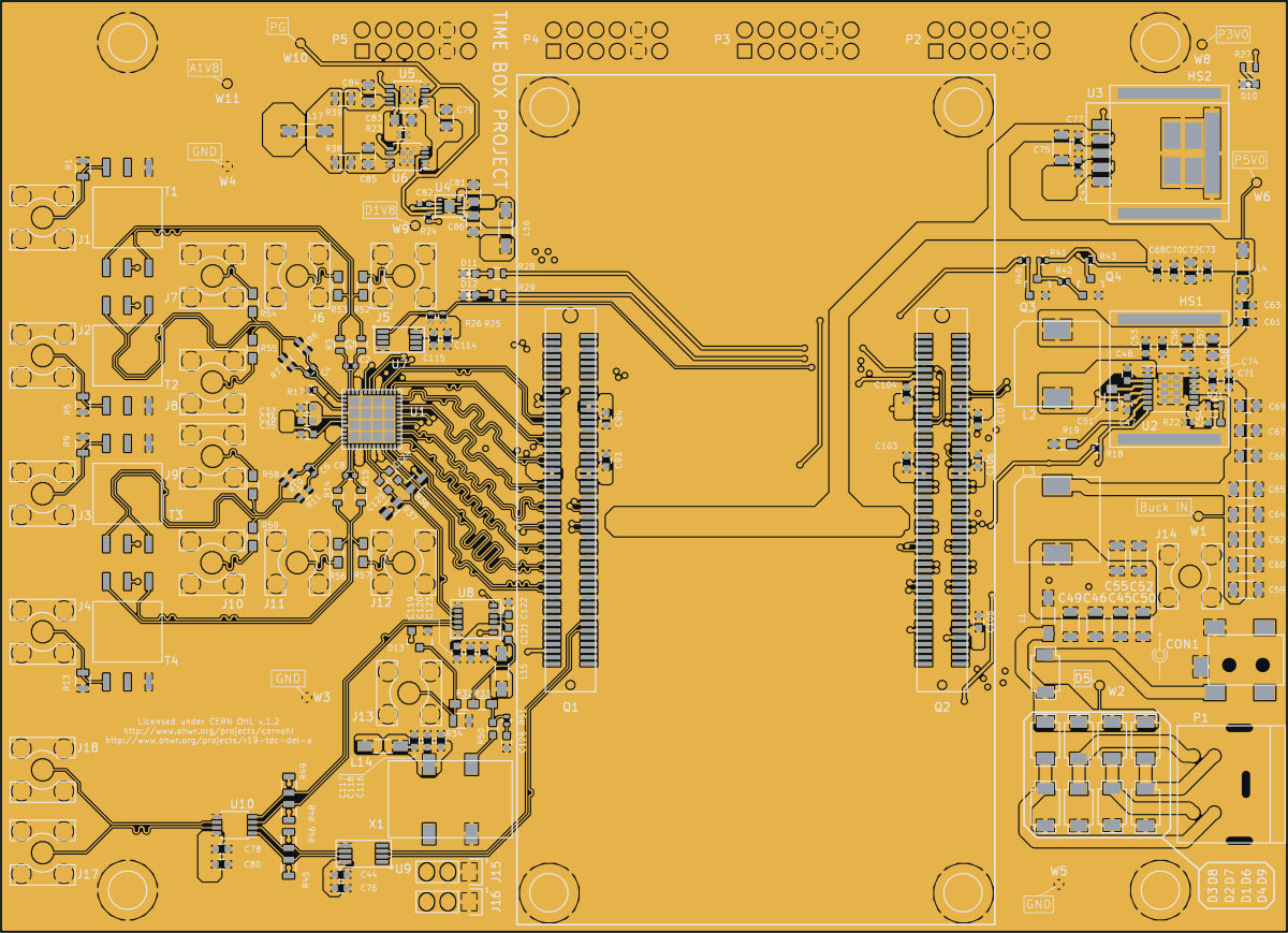
R19 TDC DEL A ADC (OHWR0065 R1) is an open-hardware circuit board from the CERN Open Hardware Repository, designed in KiCad EDA: a 4-layer board of 154 × 111.5 mm with 1344 components and 249 nets, published under CERN-OHL-1.2.
review 87% walked · 14 findings: 1 blocker · 8 major · 5 minor (40 items)
Open in the interactive viewerRead the full review
Design review
Probe recorded 14 findings: 1 blocker · 8 major · 5 minor (40 items) on this design. Each is shown here with its reasoning; the full review links every one to the pins, nets and datasheet pages it rests on.
LP3875 U3 SENSE pin is tied to GND instead of OUT, so the 3.3 V regulator has no feedback and P3V3 will rise toward the 5.2 V input
LP3875 U3 has its SENSE pin (pin 5) tied to GND instead of OUT, so the 3.3 V regulator has no feedback and P3V3 rises to about 4.8-5.0 V from the 5.2 V P5V0 input, over the absolute maximum of parts on the rail.
Where it is
Sheet 12 draws U3 (LP3875ES-3.3/NOPB, TO-263-5) with pin 5 SENSE connected to GND, and the netlist agrees.
U3 pin Net Source 1 SD /Power_Supplies_Part2/VCCIO_EN_5V netlist: component U3 2 IN P5V0 netlist: component U3 3 GND netlist: component U3 4 OUT P3V3 netlist: component U3 5 SENSE GND, nothing else joins SENSE to OUT netlist: component U3 The datasheet: the LP3875 regulates the voltage at the sense pin, and "if the sense option pin is not required, the SENSE pin must be connected to the OUT pin" (LP3875 datasheet, p.9).
What follows
With SENSE held at 0 V the error amplifier sees its output far below 3.3 V and drives the pass transistor fully on. OUT sits at the input minus dropout, about 4.8 to 5.0 V.
``
mermaid flowchart LR A["P5V0<br/>5.2 V"] --> B["U3 LP3875<br/>SENSE on GND"] B -- "P3V3 about 4.8-5.0 V" --> C["U5/U6 LT3042<br/>fine"] B --> D["U4 LP3982<br/>6 V abs max"] B --> E["U8 LTC6957<br/>3.6 V abs max"] B --> F["MicroZed VCCO_35<br/>and header outputs"]``PECL trigger outputs Q and /Q of U10 drive the SMA jacks J17/J18 with no bias or termination network
PECL trigger outputs Q and /Q of U10 (MC100EP52) drive the SMA jacks J17/J18 with no bias or termination network, so a 50 ohm-to-ground load pulls about 46 mA per output against a 50 mA maximum, and an AC-coupled or high-impedance load leaves no DC path.
Where it is
- U10 is an LVPECL D flip-flop on P3V3.
- Q (pin 7) goes only to J17 centre pin, net /TRIG_OUT0.
- /Q (pin 6) goes only to J18 centre pin, net /TRIG_OUT1.
- ECL outputs are open emitters. Nothing on the board biases them.
The numbers
Quantity Value Source Specified loading 50 ohm to VCC − 2.0 V MC100EP52 datasheet, Figure 3, p.7 Continuous output current, max 50 mA MC100EP52 datasheet, p.3 Current into 50 ohm to ground VOH 2.3 V / 50 ohm = 46 mA per output derived Why it matters
The outputs only work into whatever the cable presents. A 50 ohm-to-ground instrument runs each output at the 50 mA absolute maximum. An AC-coupled or high-impedance receiver leaves the emitter followers with no DC path and no defined level.
LP3875 U3 output is decoupled only by ceramic capacitors, while its datasheet requires 100 mOhm to 4 ohm of output-capacitor ESR and recommends tantalum
The LP3875 U3 that makes P3V3 has only ceramic capacitors on its output, whose ESR (well under 10 mΩ) sits below the stable region of the datasheet's ESR curve (about 60-90 mΩ minimum), so the 3.3 V rail that feeds the ADC LDOs, the clock buffer and the MicroZed I/O bank may oscillate.
What is on the output
Quantity Value Source Regulator U3 LP3875ES-3.3/NOPB, TO-263, fitted; U3.4 (OUT) on P3V3 netlist; BOM Bulk capacitors on P3V3 C43 10u (C_0603), C79 4u7 (C_0805), C81 4u7 (C_0805) netlist; BOM Other capacitors on P3V3 C114, C76, C80 1u; C115, C44, C78 100n (all C_0603) netlist; BOM Series resistor, tantalum, polymer or electrolytic on P3V3 none netlist; BOM Output capacitor ESR range (design example) 100 mΩ to 4 Ω, with 10 µF LP3875 datasheet p.12 Stable region, Figure 14 COUT > 10 µF; ESR lower bound about 0.06 Ω at no load rising to about 0.09 Ω at 1.5 A, upper bound about 7 Ω LP3875 datasheet p.13, Fig. 14 (read from the curve) Ceramic ESR 'typically less than 10 mΩ' LP3875 datasheet p.13 The datasheet also says, p.12: 'The output capacitor must have an equivalent series resistance (ESR) value as shown in Figure 14. Tantalum capacitors are recommended for the output capacitor', and p.13: 'Solid tantalum capacitors are recommended for use on the output because their typical ESR is very close to the ideal value required for loop compensation.'
Why the capacitors are taken as ceramic
The BOM carries value and footprint only, with no MPN or dielectric (the walker's context row on U3 says so), so the capacitor type is inferred rather than stated. The inference rests on three things: every part on P3V3 uses the generic KiCad
Capacitors_SMD:C_0603/C_0805footprint and the non-polarised 'Capacitor' symbol, not aCP_Tantalum_Case-*footprint or a polarised symbol; 10 µF in 0603 and 4.7 µF in 0805 are ordinary MLCC values; and sheet 12 annotates no capacitor type. Paralleling them only lowers the effective ESR further. If the assembly BOM actually fits a tantalum or polymer part in one of these positions, this finding falls; that is the one thing to confirm.Why it matters
An LDO whose loop compensation relies on output-capacitor ESR can oscillate with a low-ESR ceramic output. P3V3 feeds the ADC's LDOs, the clock buffer and the MicroZed I/O bank, so an unstable 3.3 V rail would show up as noise everywhere.
Options:
- fit a tantalum or polymer output capacitor (10 µF or more, ESR inside Figure 14), or add a small series resistor to a ceramic to reach the stable band
- or measure stability on hardware (load step on P3V3) and record it
- DuplicatePassivemajorOpen
'/FCI_Connector_JX2/TEMP' is pulled to 'P3V3' by 2 fitted resistors (R25 (10k), R26 (10k))
'/FCI_Connector_JX2/TEMP' is pulled to 'P3V3' by 2 fitted resistors: R25 (10k), R26 (10k) — 5k effective. A pull-up's value is specified, and two of them in parallel is not the value that was specified — presence checks are satisfied by either one and cannot see the pair. Which one is intended? Removing the duplicate, or recording that the parallel value is deliberate, both settle it; leaving two identical resistors on one node does not.
At /FCI_Connector_JX2/TEMP
- CapVoltageDeratingmajorOpen
CapVoltageDerating: 16 components×16
16 checked by the review by evaluation@esharp.se — 16 different reasons
At C45, C46, C49, C50, C52, C55 and 10 more
Each finding, with its own headline
C45C45 sits on a 12 V rail and its voltage rating is not in the BOM
C45: on a 12 V rail but its voltage rating is not stated in the BOM — add it so the rating can be compared to the rail at all. No datasheet is on file for this part; the BOM short-spec is the source.
C46C46 sits on a 12 V rail and its voltage rating is not in the BOM
C46: on a 12 V rail but its voltage rating is not stated in the BOM — add it so the rating can be compared to the rail at all. No datasheet is on file for this part; the BOM short-spec is the source.
C49C49 sits on a 12 V rail and its voltage rating is not in the BOM
C49: on a 12 V rail but its voltage rating is not stated in the BOM — add it so the rating can be compared to the rail at all. No datasheet is on file for this part; the BOM short-spec is the source.
C50C50 sits on a 12 V rail and its voltage rating is not in the BOM
C50: on a 12 V rail but its voltage rating is not stated in the BOM — add it so the rating can be compared to the rail at all. No datasheet is on file for this part; the BOM short-spec is the source.
C52C52 sits on a 12 V rail and its voltage rating is not in the BOM
C52: on a 12 V rail but its voltage rating is not stated in the BOM — add it so the rating can be compared to the rail at all. No datasheet is on file for this part; the BOM short-spec is the source.
C55C55 sits on a 12 V rail and its voltage rating is not in the BOM
C55: on a 12 V rail but its voltage rating is not stated in the BOM — add it so the rating can be compared to the rail at all. No datasheet is on file for this part; the BOM short-spec is the source.
C59C59 sits on a 12 V rail and its voltage rating is not in the BOM
C59: on a 12 V rail but its voltage rating is not stated in the BOM — add it so the rating can be compared to the rail at all. No datasheet is on file for this part; the BOM short-spec is the source.
C60C60 sits on a 12 V rail and its voltage rating is not in the BOM
C60: on a 12 V rail but its voltage rating is not stated in the BOM — add it so the rating can be compared to the rail at all. No datasheet is on file for this part; the BOM short-spec is the source.
C62C62 sits on a 12 V rail and its voltage rating is not in the BOM
C62: on a 12 V rail but its voltage rating is not stated in the BOM — add it so the rating can be compared to the rail at all. No datasheet is on file for this part; the BOM short-spec is the source.
C64C64 sits on a 12 V rail and its voltage rating is not in the BOM
C64: on a 12 V rail but its voltage rating is not stated in the BOM — add it so the rating can be compared to the rail at all. No datasheet is on file for this part; the BOM short-spec is the source.
C65C65 sits on a 12 V rail and its voltage rating is not in the BOM
C65: on a 12 V rail but its voltage rating is not stated in the BOM — add it so the rating can be compared to the rail at all. No datasheet is on file for this part; the BOM short-spec is the source.
C66C66 sits on a 12 V rail and its voltage rating is not in the BOM
C66: on a 12 V rail but its voltage rating is not stated in the BOM — add it so the rating can be compared to the rail at all. No datasheet is on file for this part; the BOM short-spec is the source.
C67C67 sits on a 12 V rail and its voltage rating is not in the BOM
C67: on a 12 V rail but its voltage rating is not stated in the BOM — add it so the rating can be compared to the rail at all. No datasheet is on file for this part; the BOM short-spec is the source.
C69C69 sits on a 12 V rail and its voltage rating is not in the BOM
C69: on a 12 V rail but its voltage rating is not stated in the BOM — add it so the rating can be compared to the rail at all. No datasheet is on file for this part; the BOM short-spec is the source.
C71C71 sits on a 12 V rail and its voltage rating is not in the BOM
C71: on a 12 V rail but its voltage rating is not stated in the BOM — add it so the rating can be compared to the rail at all. No datasheet is on file for this part; the BOM short-spec is the source.
C74C74 sits on a 12 V rail and its voltage rating is not in the BOM
C74: on a 12 V rail but its voltage rating is not stated in the BOM — add it so the rating can be compared to the rail at all. No datasheet is on file for this part; the BOM short-spec is the source.
- FiducialMissingmajorOpen
FiducialMissing: 2 boards×2
2 checked by the review by evaluation@esharp.se — 2 different reasons
At bottom, top
Each finding, with its own headline
bottomThe bottom side carries 60 SMT component(s) and no fiducial was found on it
The bottom side carries 60 SMT component(s) but no fiducial was found on it — a placement machine has no optical reference to align to. Probe found no pad labelled .pad_usage=g_fiducial/l_fiducial (basis pad_usage); no single-pad, netless, undrilled component whose 0.5-3 mm round pad has a concentric solder-mask opening at least 1.5x its diameter with no other copper inside it (basis geometry); and no component whose refdes starts FID or whose part or package name contains FIDUCIAL (basis footprint-name). If your library names fiducials something Probe does not recognise, mark this benign — disposition_finding(rule='FiducialMissing', entity='bottom', status='benign', reason=…) — the name match only ever silences this check, it never asserts anything. If the side really has no fiducial, say so with status='confirmed': that answers the finding and keeps it gating release.
topThe top side carries 136 SMT component(s) and no fiducial was found on it
The top side carries 136 SMT component(s) but no fiducial was found on it — a placement machine has no optical reference to align to. Probe found no pad labelled .pad_usage=g_fiducial/l_fiducial (basis pad_usage); no single-pad, netless, undrilled component whose 0.5-3 mm round pad has a concentric solder-mask opening at least 1.5x its diameter with no other copper inside it (basis geometry); and no component whose refdes starts FID or whose part or package name contains FIDUCIAL (basis footprint-name). If your library names fiducials something Probe does not recognise, mark this benign — disposition_finding(rule='FiducialMissing', entity='top', status='benign', reason=…) — the name match only ever silences this check, it never asserts anything. If the side really has no fiducial, say so with status='confirmed': that answers the finding and keeps it gating release.
- PartLifecyclemajorOpen
PartLifecycle: 6 part numbers×6
5 Obsolete, 1 Discontinued at DigiKey · on 20 placements
At D13, J1, J10, P1, U1, U8
Each finding, with its own headline
D13HSMS-2822-TR1G on D13: the distributor catalogue reports "Obsolete" for Broadcom Limited's HSMS-2822-TR1G
HSMS-2822-TR1G on D13: the distributor catalogue reports "Obsolete" for Broadcom Limited's HSMS-2822-TR1G — a sourcing/longevity risk to confirm against the MANUFACTURER before acting. This board's BOM names no manufacturer for it, so whether that is the fitted maker's product was not checked. A distributor delisting is not the same claim as the part being unavailable; check the vendor's own lifecycle/product-change notice for the status and any named successor. Re-read the source: GET /api/odb/parts/HSMS-2822-TR1G/providers (which provider said it, the maker and part number it matched, its own words, and when we asked). THE LAST BUY DATE HAS PASSED (2018-06-01, 3,089 day(s) ago), so this is a substitution rather than a buy. The distributor reports NONE left. No approved alternate is recorded for this position.
J15-1814400-1 on 6 placements (J1, J17, J18, J2, J3, J4): the distributor catalogue reports "Obsolete" for TE Connectivity AMP Connectors's 5-1814400-1
5-1814400-1 on 6 placements (J1, J17, J18, J2, J3, J4): the distributor catalogue reports "Obsolete" for TE Connectivity AMP Connectors's 5-1814400-1 — a sourcing/longevity risk to confirm against the MANUFACTURER before acting. This board's BOM names no manufacturer for it, so whether that is the fitted maker's product was not checked. A distributor delisting is not the same claim as the part being unavailable; check the vendor's own lifecycle/product-change notice for the status and any named successor. Re-read the source: GET /api/odb/parts/5-1814400-1/providers (which provider said it, the maker and part number it matched, its own words, and when we asked). THE LAST BUY DATE HAS PASSED (2020-03-01, 2,450 day(s) ago), so this is a substitution rather than a buy. The distributor reports NONE left. No approved alternate is recorded for this position.
J105-1814832-1 on 10 placements (J10, J11, J12, J13, J14, J5, J6, J7, …): the distributor catalogue reports "Obsolete" for TE Connectivity AMP Connectors's 5-1814832-1
5-1814832-1 on 10 placements (J10, J11, J12, J13, J14, J5, J6, J7, …): the distributor catalogue reports "Obsolete" for TE Connectivity AMP Connectors's 5-1814832-1 — a sourcing/longevity risk to confirm against the MANUFACTURER before acting. This board's BOM names no manufacturer for it, so whether that is the fitted maker's product was not checked. A distributor delisting is not the same claim as the part being unavailable; check the vendor's own lifecycle/product-change notice for the status and any named successor. Re-read the source: GET /api/odb/parts/5-1814832-1/providers (which provider said it, the maker and part number it matched, its own words, and when we asked). THE LAST BUY DATE HAS PASSED (2020-01-01, 2,510 day(s) ago), so this is a substitution rather than a buy. The distributor reports NONE left. No approved alternate is recorded for this position.
P1MD-40SMK on P1: the distributor catalogue reports "Obsolete" for Same Sky (Formerly CUI Devices)'s MD-40SMK
MD-40SMK on P1: the distributor catalogue reports "Obsolete" for Same Sky (Formerly CUI Devices)'s MD-40SMK — a sourcing/longevity risk to confirm against the MANUFACTURER before acting. This board's BOM names no manufacturer for it, so whether that is the fitted maker's product was not checked. A distributor delisting is not the same claim as the part being unavailable; check the vendor's own lifecycle/product-change notice for the status and any named successor. Re-read the source: GET /api/odb/parts/MD-40SMK/providers (which provider said it, the maker and part number it matched, its own words, and when we asked). No approved alternate is recorded for this position.
U1AD9253BCPZ-125 on U1: the distributor catalogue reports "Discontinued at DigiKey" for Analog Devices Inc.'s AD9253BCPZ-125
AD9253BCPZ-125 on U1: the distributor catalogue reports "Discontinued at DigiKey" for Analog Devices Inc.'s AD9253BCPZ-125 — a sourcing/longevity risk to confirm against the MANUFACTURER before acting. This board's BOM names no manufacturer for it, so whether that is the fitted maker's product was not checked. A distributor delisting is not the same claim as the part being unavailable; check the vendor's own lifecycle/product-change notice for the status and any named successor. Re-read the source: GET /api/odb/parts/AD9253BCPZ-125/providers (which provider said it, the maker and part number it matched, its own words, and when we asked). No approved alternate is recorded for this position.
U8LTC6957IMS-1#PBF on U8: the distributor catalogue reports "Obsolete" for Analog Devices Inc.'s LTC6957IMS-1#PBF
LTC6957IMS-1#PBF on U8: the distributor catalogue reports "Obsolete" for Analog Devices Inc.'s LTC6957IMS-1#PBF — a sourcing/longevity risk to confirm against the MANUFACTURER before acting. This board's BOM names no manufacturer for it, so whether that is the fitted maker's product was not checked. A distributor delisting is not the same claim as the part being unavailable; check the vendor's own lifecycle/product-change notice for the status and any named successor. Re-read the source: GET /api/odb/parts/LTC6957IMS-1#PBF/providers (which provider said it, the maker and part number it matched, its own words, and when we asked). THE LAST BUY DATE HAS PASSED (2025-01-17, 667 day(s) ago), so this is a substitution rather than a buy. The distributor reports NONE left. No approved alternate is recorded for this position.
- ReferencePlaneDiscontinuitymajorOpen
ReferencePlaneDiscontinuity: 6 boards×6
e.g. “5 nets change reference between A1V8 and GND at 5 vias, none with a reference that continues across (fastest: /ADC1-Rev4/SPI2 at 2 ns 10-90 %, suggested by its name)” · 6 different statements
At refchange:A1V8|GND, refchange:D1V8|GND, refchange:GND|P3V3, refchange:GND|P5V0, split@IN2.CU:D1V8|P3V3, split@IN2.CU:P3V3|P5V0
Each finding, with its own headline
refchange:A1V8|GND5 nets change reference between A1V8 and GND at 5 vias, none with a reference that continues across (fastest: /ADC1-Rev4/SPI2 at 2 ns 10-90 %, suggested by its name)
At 5 via(s), on 5 net(s), the signal leaves a layer referenced by one of A1V8 and GND for a layer referenced by the other, and no plane references both layers. Different nets: no via can carry the return across; only decoupling between the two planes near the via can. The capacitor carrying the return across was measured at each via, at the knee of the crossing net's edge against 50 ohm assumed: 5 with none. 5 of them at an ASSUMED edge (no edge on file for the net): state one (net_timing_state) and it is re-read. One decision covers the pair: whether A1V8 and GND are decoupled to each other near these vias. A via whose layers have more references than these two is a site of each pair it joins. None is partial: at every one, no reference continues across the via.
- '/ADC1-Rev4/SPI2' at (118.61, -85.39), F.CU -> B.CU: GND on IN1.CU to A1V8 on IN2.CU; pure, no reference continues across; stitching none, 30.1 mm of track past the via on B.CU: At the 5 GHz knee of a 100 ps edge (2 ns 10-90 %, assumed: no edge is on file for the net) no capacitor carries the return; only the planes do. A1V8 and GND are not a thin pair (at most 0.2 mm), so their own capacitance does not carry the return. To serve it, change layers across the same plane, or move the signal to a layer referenced to ground. Measured for reference: C14 (1 uF 0603) 0.8 mm away: 0.35 nH in the 0.480 mm cavity + 0.51 nH ESL + 0.68 nH mounting (pad 0.10 nH + no via of the first net within 1 mm of its pad: the study's 0.6 nH per mm of 0.96 mm depth, ASSUMED): 48.1 ohm at the knee, 96 % of 50 ohm (assumed track impedance). None.
- '/inputC/MiddlePoint' at (90.63, -106.74), F.CU -> B.CU: GND on IN1.CU to A1V8 on IN2.CU; pure, no reference continues across; stitching none, 3.0 mm of track past the via on B.CU: At the 5 GHz knee of a 100 ps edge (20 ns 10-90 %, assumed: no edge is on file for the net) no capacitor carries the return; only the planes do. A1V8 and GND are not a thin pair (at most 0.2 mm), so their own capacitance does not carry the return. To serve it, change layers across the same plane, or move the signal to a layer referenced to ground. None.
- '/inputB/MiddlePoint' at (90.57, -78.24), F.CU -> B.CU: GND on IN1.CU to A1V8 on IN2.CU; pure, no reference continues across; stitching none, 2.9 mm of track past the via on B.CU: At the 5 GHz knee of a 100 ps edge (20 ns 10-90 %, assumed: no edge is on file for the net) no capacitor carries the return; only the planes do. A1V8 and GND are not a thin pair (at most 0.2 mm), so their own capacitance does not carry the return. To serve it, change layers across the same plane, or move the signal to a layer referenced to ground. None.
- '/inputD/MiddlePoint' at (90.63, -111.24), F.CU -> B.CU: GND on IN1.CU to A1V8 on IN2.CU; pure, no reference continues across; stitching none, 2.8 mm of track past the via on B.CU: At the 5 GHz knee of a 100 ps edge (20 ns 10-90 %, assumed: no edge is on file for the net) no capacitor carries the return; only the planes do. A1V8 and GND are not a thin pair (at most 0.2 mm), so their own capacitance does not carry the return. To serve it, change layers across the same plane, or move the signal to a layer referenced to ground. None.
- '/inputA/MiddlePoint' at (90.58, -73.72), F.CU -> B.CU: GND on IN1.CU to A1V8 on IN2.CU; pure, no reference continues across; stitching none, 2.8 mm of track past the via on B.CU: At the 5 GHz knee of a 100 ps edge (20 ns 10-90 %, assumed: no edge is on file for the net) no capacitor carries the return; only the planes do. A1V8 and GND are not a thin pair (at most 0.2 mm), so their own capacitance does not carry the return. To serve it, change layers across the same plane, or move the signal to a layer referenced to ground. None.
Every site is a row of this finding's evidence, keyed by net, layers and position. GET /api/odb/boards/66/reference-planes?group=refchange%3AA1V8%7CGND serves each with its own layer_image region; all of them lie in x 88.57..120.61, y -113.24..-71.72 mm (board frame, Y up).
The reference on each layer is the first plane the track meets leaving the via, anti-pads and the net's own copper skipped. Whether it matters depends on each signal's edge rate, which nothing on file states for these nets: a slow static line crosses a split harmlessly, a fast edge does not.
refchange:D1V8|GND9 nets change reference between D1V8 and GND at 16 vias, none with a reference that continues across (fastest: Net-(J15-Pad2) at 100 ps 10-90 %, ASSUMED)
At 16 via(s), on 9 net(s), the signal leaves a layer referenced by one of D1V8 and GND for a layer referenced by the other, and no plane references both layers. Different nets: no via can carry the return across; only decoupling between the two planes near the via can. The capacitor carrying the return across was measured at each via, at the knee of the crossing net's edge against 50 ohm assumed: 16 with none. 16 of them at an ASSUMED edge (no edge on file for the net): state one (net_timing_state) and it is re-read. One decision covers the pair: whether D1V8 and GND are decoupled to each other near these vias. A via whose layers have more references than these two is a site of each pair it joins. None is partial: at every one, no reference continues across the via.
- 'Net-(J15-Pad2)' at (131.83, -112.6), F.CU -> B.CU: GND on IN1.CU to D1V8 on IN2.CU; pure, no reference continues across; stitching none, 35.1 mm of track past the via on B.CU: At the 5 GHz knee of a 100 ps edge (100 ps 10-90 %, assumed: no edge is on file for the net) no capacitor carries the return; only the planes do. D1V8 and GND are not a thin pair (at most 0.2 mm), so their own capacitance does not carry the return. To serve it, change layers across the same plane, or move the signal to a layer referenced to ground. None.
- '/ADC1-Rev4/DATA_CLK3' at (136.71, -105.32), F.CU -> B.CU: GND on IN1.CU to D1V8 on IN2.CU; pure, no reference continues across; stitching none, 33.5 mm of track past the via on B.CU: At the 5 GHz knee of a 100 ps edge (1 ns 10-90 %, assumed: no edge is on file for the net) no capacitor carries the return; only the planes do. D1V8 and GND are not a thin pair (at most 0.2 mm), so their own capacitance does not carry the return. To serve it, change layers across the same plane, or move the signal to a layer referenced to ground. None.
- '/ADC1-Rev4/DATA_CLK3' at (123.98, -92.78), F.CU -> B.CU: GND on IN1.CU to D1V8 on IN2.CU; pure, no reference continues across; stitching none, 33.5 mm of track past the via on B.CU: At the 5 GHz knee of a 100 ps edge (1 ns 10-90 %, assumed: no edge is on file for the net) no capacitor carries the return; only the planes do. D1V8 and GND are not a thin pair (at most 0.2 mm), so their own capacitance does not carry the return. To serve it, change layers across the same plane, or move the signal to a layer referenced to ground. Measured for reference: C33 (1 uF 0603) 1.6 mm away: 0.49 nH in the 0.480 mm cavity + 0.51 nH ESL + 0.68 nH mounting (pad 0.10 nH + no via of the first net within 1 mm of its pad: the study's 0.6 nH per mm of 0.96 mm depth, ASSUMED): 52.7 ohm at the knee, 105 % of 50 ohm (assumed track impedance). None.
- '/ADC1-Rev4/DATA_CLK2' at (136.18, -104.79), F.CU -> B.CU: GND on IN1.CU to D1V8 on IN2.CU; pure, no reference continues across; stitching none, 32.3 mm of track past the via on B.CU: At the 5 GHz knee of a 100 ps edge (1 ns 10-90 %, assumed: no edge is on file for the net) no capacitor carries the return; only the planes do. D1V8 and GND are not a thin pair (at most 0.2 mm), so their own capacitance does not carry the return. To serve it, change layers across the same plane, or move the signal to a layer referenced to ground. None.
- '/ADC1-Rev4/DATA_CLK2' at (124.51, -92.25), F.CU -> B.CU: GND on IN1.CU to D1V8 on IN2.CU; pure, no reference continues across; stitching none, 32.3 mm of track past the via on B.CU: At the 5 GHz knee of a 100 ps edge (1 ns 10-90 %, assumed: no edge is on file for the net) no capacitor carries the return; only the planes do. D1V8 and GND are not a thin pair (at most 0.2 mm), so their own capacitance does not carry the return. To serve it, change layers across the same plane, or move the signal to a layer referenced to ground. Measured for reference: C33 (1 uF 0603) 2.4 mm away: 0.56 nH in the 0.480 mm cavity + 0.51 nH ESL + 0.68 nH mounting (pad 0.10 nH + no via of the first net within 1 mm of its pad: the study's 0.6 nH per mm of 0.96 mm depth, ASSUMED): 54.9 ohm at the knee, 110 % of 50 ohm (assumed track impedance). None.
- '/ADC1-Rev4/SPI0' at (142.83, -101.68), F.CU -> B.CU: GND on IN1.CU to D1V8 on IN2.CU; pure, no reference continues across; stitching none, 31.9 mm of track past the via on B.CU: At the 5 GHz knee of a 100 ps edge (2 ns 10-90 %, assumed: no edge is on file for the net) no capacitor carries the return; only the planes do. D1V8 and GND are not a thin pair (at most 0.2 mm), so their own capacitance does not carry the return. To serve it, change layers across the same plane, or move the signal to a layer referenced to ground. None.
- '/ADC1-Rev4/SPI0' at (123.38, -84.71), F.CU -> B.CU: GND on IN1.CU to D1V8 on IN2.CU; pure, no reference continues across; stitching none, 31.9 mm of track past the via on B.CU: At the 5 GHz knee of a 100 ps edge (2 ns 10-90 %, assumed: no edge is on file for the net) no capacitor carries the return; only the planes do. D1V8 and GND are not a thin pair (at most 0.2 mm), so their own capacitance does not carry the return. To serve it, change layers across the same plane, or move the signal to a layer referenced to ground. Measured for reference: C34 (1 uF 0603) 2.4 mm away: 0.56 nH in the 0.480 mm cavity + 0.51 nH ESL + 0.68 nH mounting (pad 0.10 nH + no via of the first net within 1 mm of its pad: the study's 0.6 nH per mm of 0.96 mm depth, ASSUMED): 54.9 ohm at the knee, 110 % of 50 ohm (assumed track impedance). None.
- '/ADC1-Rev4/SPI2' at (141.97, -88.44), F.CU -> B.CU: GND on IN1.CU to D1V8 on IN2.CU; pure, no reference continues across; stitching none, 30.1 mm of track past the via on B.CU: At the 5 GHz knee of a 100 ps edge (2 ns 10-90 %, assumed: no edge is on file for the net) no capacitor carries the return; only the planes do. D1V8 and GND are not a thin pair (at most 0.2 mm), so their own capacitance does not carry the return. To serve it, change layers across the same plane, or move the signal to a layer referenced to ground. None.
- '/ADC1-Rev4/SPI1' at (142.3, -102.21), F.CU -> B.CU: GND on IN1.CU to D1V8 on IN2.CU; pure, no reference continues across; stitching none, 30.0 mm of track past the via on B.CU: At the 5 GHz knee of a 100 ps edge (2 ns 10-90 %, assumed: no edge is on file for the net) no capacitor carries the return; only the planes do. D1V8 and GND are not a thin pair (at most 0.2 mm), so their own capacitance does not carry the return. To serve it, change layers across the same plane, or move the signal to a layer referenced to ground. None.
- '/ADC1-Rev4/SPI1' at (122.45, -84.3), F.CU -> B.CU: GND on IN1.CU to D1V8 on IN2.CU; pure, no reference continues across; stitching none, 30.0 mm of track past the via on B.CU: At the 5 GHz knee of a 100 ps edge (2 ns 10-90 %, assumed: no edge is on file for the net) no capacitor carries the return; only the planes do. D1V8 and GND are not a thin pair (at most 0.2 mm), so their own capacitance does not carry the return. To serve it, change layers across the same plane, or move the signal to a layer referenced to ground. Measured for reference: C34 (1 uF 0603) 1.8 mm away: 0.51 nH in the 0.480 mm cavity + 0.51 nH ESL + 0.68 nH mounting (pad 0.10 nH + no via of the first net within 1 mm of its pad: the study's 0.6 nH per mm of 0.96 mm depth, ASSUMED): 53.1 ohm at the knee, 106 % of 50 ohm (assumed track impedance). None.
- '/ADC1-Rev4/DATA_CLK1' at (125.46, -92.21), F.CU -> B.CU: GND on IN1.CU to D1V8 on IN2.CU; pure, no reference continues across; stitching none, 28.2 mm of track past the via on B.CU: At the 5 GHz knee of a 100 ps edge (1 ns 10-90 %, assumed: no edge is on file for the net) no capacitor carries the return; only the planes do. D1V8 and GND are not a thin pair (at most 0.2 mm), so their own capacitance does not carry the return. To serve it, change layers across the same plane, or move the signal to a layer referenced to ground. None.
- '/ADC1-Rev4/DATA_CLK1' at (142.55, -105.06), F.CU -> B.CU: GND on IN1.CU to D1V8 on IN2.CU; pure, no reference continues across; stitching none, 28.2 mm of track past the via on B.CU: At the 5 GHz knee of a 100 ps edge (1 ns 10-90 %, assumed: no edge is on file for the net) no capacitor carries the return; only the planes do. D1V8 and GND are not a thin pair (at most 0.2 mm), so their own capacitance does not carry the return. To serve it, change layers across the same plane, or move the signal to a layer referenced to ground. None.
- and 4 more
Every site is a row of this finding's evidence, keyed by net, layers and position. GET /api/odb/boards/66/reference-planes?group=refchange%3AD1V8%7CGND serves each with its own layer_image region; all of them lie in x 118.89..144.83, y -114.6..-82.3 mm (board frame, Y up).
The reference on each layer is the first plane the track meets leaving the via, anti-pads and the net's own copper skipped. Whether it matters depends on each signal's edge rate, which nothing on file states for these nets: a slow static line crosses a split harmlessly, a fast edge does not.
refchange:GND|P3V334 nets change reference between GND and P3V3 at 46 vias, none with a reference that continues across (fastest: /FCI_Connector_JX2/CONN0 at 100 ps 10-90 %, ASSUMED)
At 46 via(s), on 34 net(s), the signal leaves a layer referenced by one of GND and P3V3 for a layer referenced by the other, and no plane references both layers. Different nets: no via can carry the return across; only decoupling between the two planes near the via can. The capacitor carrying the return across was measured at each via, at the knee of the crossing net's edge against 50 ohm assumed: 46 with none. 46 of them at an ASSUMED edge (no edge on file for the net): state one (net_timing_state) and it is re-read. One decision covers the pair: whether GND and P3V3 are decoupled to each other near these vias. A via whose layers have more references than these two is a site of each pair it joins. None is partial: at every one, no reference continues across the via.
- '/FCI_Connector_JX2/PWR_GOOD' at (182.99, -117.02), F.CU -> B.CU: GND on IN1.CU to P3V3 on IN2.CU; pure, no reference continues across; stitching none, 109.4 mm of track past the via on B.CU: At the 5 GHz knee of a 100 ps edge (100 ps 10-90 %, assumed: no edge is on file for the net) no capacitor carries the return; only the planes do. GND and P3V3 are not a thin pair (at most 0.2 mm), so their own capacitance does not carry the return. To serve it, change layers across the same plane, or move the signal to a layer referenced to ground. None.
- '/FCI_Connector_JX2/PWR_GOOD' at (224.33, -47.99), F.CU -> B.CU: GND on IN1.CU to P3V3 on IN2.CU; pure, no reference continues across; stitching none, 109.4 mm of track past the via on B.CU: At the 5 GHz knee of a 100 ps edge (100 ps 10-90 %, assumed: no edge is on file for the net) no capacitor carries the return; only the planes do. GND and P3V3 are not a thin pair (at most 0.2 mm), so their own capacitance does not carry the return. To serve it, change layers across the same plane, or move the signal to a layer referenced to ground. None.
- '/FCI_Connector_JX2/CONN4' at (186.16, -109.92), F.CU -> B.CU: GND on IN1.CU to P3V3 on IN2.CU; pure, no reference continues across; stitching none, 98.2 mm of track past the via on B.CU: At the 5 GHz knee of a 100 ps edge (100 ps 10-90 %, assumed: no edge is on file for the net) no capacitor carries the return; only the planes do. GND and P3V3 are not a thin pair (at most 0.2 mm), so their own capacitance does not carry the return. To serve it, change layers across the same plane, or move the signal to a layer referenced to ground. None.
- '/FCI_Connector_JX2/CONN6' at (190.52, -109.92), F.CU -> B.CU: GND on IN1.CU to P3V3 on IN2.CU; pure, no reference continues across; stitching none, 97.9 mm of track past the via on B.CU: At the 5 GHz knee of a 100 ps edge (100 ps 10-90 %, assumed: no edge is on file for the net) no capacitor carries the return; only the planes do. GND and P3V3 are not a thin pair (at most 0.2 mm), so their own capacitance does not carry the return. To serve it, change layers across the same plane, or move the signal to a layer referenced to ground. None.
- '/FCI_Connector_JX2/CONN5' at (186.18, -109.17), F.CU -> B.CU: GND on IN1.CU to P3V3 on IN2.CU; pure, no reference continues across; stitching none, 95.6 mm of track past the via on B.CU: At the 5 GHz knee of a 100 ps edge (100 ps 10-90 %, assumed: no edge is on file for the net) no capacitor carries the return; only the planes do. GND and P3V3 are not a thin pair (at most 0.2 mm), so their own capacitance does not carry the return. To serve it, change layers across the same plane, or move the signal to a layer referenced to ground. None.
- '/FCI_Connector_JX2/CONN7' at (190.55, -109.11), F.CU -> B.CU: GND on IN1.CU to P3V3 on IN2.CU; pure, no reference continues across; stitching none, 95.3 mm of track past the via on B.CU: At the 5 GHz knee of a 100 ps edge (100 ps 10-90 %, assumed: no edge is on file for the net) no capacitor carries the return; only the planes do. GND and P3V3 are not a thin pair (at most 0.2 mm), so their own capacitance does not carry the return. To serve it, change layers across the same plane, or move the signal to a layer referenced to ground. None.
- '/FCI_Connector_JX2/CONN2' at (187.59, -112.31), F.CU -> B.CU: GND on IN1.CU to P3V3 on IN2.CU; pure, no reference continues across; stitching none, 95.2 mm of track past the via on B.CU: At the 5 GHz knee of a 100 ps edge (100 ps 10-90 %, assumed: no edge is on file for the net) no capacitor carries the return; only the planes do. GND and P3V3 are not a thin pair (at most 0.2 mm), so their own capacitance does not carry the return. To serve it, change layers across the same plane, or move the signal to a layer referenced to ground. None.
- '/FCI_Connector_JX2/CONN0' at (182.83, -112.3), F.CU -> B.CU: GND on IN1.CU to P3V3 on IN2.CU; pure, no reference continues across; stitching none, 94.7 mm of track past the via on B.CU: At the 5 GHz knee of a 100 ps edge (100 ps 10-90 %, assumed: no edge is on file for the net) no capacitor carries the return; only the planes do. GND and P3V3 are not a thin pair (at most 0.2 mm), so their own capacitance does not carry the return. To serve it, change layers across the same plane, or move the signal to a layer referenced to ground. None.
- '/FCI_Connector_JX2/CONN3' at (187.55, -111.46), F.CU -> B.CU: GND on IN1.CU to P3V3 on IN2.CU; pure, no reference continues across; stitching none, 93.1 mm of track past the via on B.CU: At the 5 GHz knee of a 100 ps edge (100 ps 10-90 %, assumed: no edge is on file for the net) no capacitor carries the return; only the planes do. GND and P3V3 are not a thin pair (at most 0.2 mm), so their own capacitance does not carry the return. To serve it, change layers across the same plane, or move the signal to a layer referenced to ground. None.
- '/FCI_Connector_JX2/CONN1' at (182.94, -111.39), F.CU -> B.CU: GND on IN1.CU to P3V3 on IN2.CU; pure, no reference continues across; stitching none, 92.3 mm of track past the via on B.CU: At the 5 GHz knee of a 100 ps edge (100 ps 10-90 %, assumed: no edge is on file for the net) no capacitor carries the return; only the planes do. GND and P3V3 are not a thin pair (at most 0.2 mm), so their own capacitance does not carry the return. To serve it, change layers across the same plane, or move the signal to a layer referenced to ground. None.
- '/FCI_Connector_JX1/PWR_ENABLE' at (137.28, -119.65), F.CU -> B.CU: GND on IN1.CU to P3V3 on IN2.CU; pure, no reference continues across; stitching none, 75.7 mm of track past the via on B.CU: At the 5 GHz knee of a 100 ps edge (20 ns 10-90 %, assumed: no edge is on file for the net) no capacitor carries the return; only the planes do. GND and P3V3 are not a thin pair (at most 0.2 mm), so their own capacitance does not carry the return. To serve it, change layers across the same plane, or move the signal to a layer referenced to ground. None.
- '/FCI_Connector_JX1/PWR_ENABLE' at (189.48, -125.55), F.CU -> B.CU: GND on IN1.CU to P3V3 on IN2.CU; pure, no reference continues across; stitching none, 75.7 mm of track past the via on B.CU: At the 5 GHz knee of a 100 ps edge (20 ns 10-90 %, assumed: no edge is on file for the net) no capacitor carries the return; only the planes do. GND and P3V3 are not a thin pair (at most 0.2 mm), so their own capacitance does not carry the return. To serve it, change layers across the same plane, or move the signal to a layer referenced to ground. None.
- and 34 more
Every site is a row of this finding's evidence, keyed by net, layers and position. GET /api/odb/boards/66/reference-planes?group=refchange%3AGND%7CP3V3 serves each with its own layer_image region; all of them lie in x 106.68..226.33, y -147.45..-45.99 mm (board frame, Y up).
The reference on each layer is the first plane the track meets leaving the via, anti-pads and the net's own copper skipped. Whether it matters depends on each signal's edge rate, which nothing on file states for these nets: a slow static line crosses a split harmlessly, a fast edge does not.
refchange:GND|P5V09 nets change reference between GND and P5V0 at 9 vias, none with a reference that continues across (fastest: /FCI_Connector_JX2/CONN10 at 100 ps 10-90 %, ASSUMED)
At 9 via(s), on 9 net(s), the signal leaves a layer referenced by one of GND and P5V0 for a layer referenced by the other, and no plane references both layers. Different nets: no via can carry the return across; only decoupling between the two planes near the via can. The capacitor carrying the return across was measured at each via, at the knee of the crossing net's edge against 50 ohm assumed: 9 with none. 9 of them at an ASSUMED edge (no edge on file for the net): state one (net_timing_state) and it is re-read. One decision covers the pair: whether GND and P5V0 are decoupled to each other near these vias. A via whose layers have more references than these two is a site of each pair it joins. None is partial: at every one, no reference continues across the via.
- '/FCI_Connector_JX2/CONN14' at (190.56, -105.12), F.CU -> B.CU: GND on IN1.CU to P5V0 on IN2.CU; pure, no reference continues across; stitching none, 86.0 mm of track past the via on B.CU: At the 5 GHz knee of a 100 ps edge (100 ps 10-90 %, assumed: no edge is on file for the net) no capacitor carries the return; only the planes do. GND and P5V0 are not a thin pair (at most 0.2 mm), so their own capacitance does not carry the return. To serve it, change layers across the same plane, or move the signal to a layer referenced to ground. None.
- '/FCI_Connector_JX2/CONN15' at (190.58, -104.29), F.CU -> B.CU: GND on IN1.CU to P5V0 on IN2.CU; pure, no reference continues across; stitching none, 83.4 mm of track past the via on B.CU: At the 5 GHz knee of a 100 ps edge (100 ps 10-90 %, assumed: no edge is on file for the net) no capacitor carries the return; only the planes do. GND and P5V0 are not a thin pair (at most 0.2 mm), so their own capacitance does not carry the return. To serve it, change layers across the same plane, or move the signal to a layer referenced to ground. None.
- '/FCI_Connector_JX2/CONN12' at (186.03, -105.09), F.CU -> B.CU: GND on IN1.CU to P5V0 on IN2.CU; pure, no reference continues across; stitching none, 83.0 mm of track past the via on B.CU: At the 5 GHz knee of a 100 ps edge (100 ps 10-90 %, assumed: no edge is on file for the net) no capacitor carries the return; only the planes do. GND and P5V0 are not a thin pair (at most 0.2 mm), so their own capacitance does not carry the return. To serve it, change layers across the same plane, or move the signal to a layer referenced to ground. None.
- '/FCI_Connector_JX2/CONN10' at (187.51, -107.35), F.CU -> B.CU: GND on IN1.CU to P5V0 on IN2.CU; pure, no reference continues across; stitching none, 80.7 mm of track past the via on B.CU: At the 5 GHz knee of a 100 ps edge (100 ps 10-90 %, assumed: no edge is on file for the net) no capacitor carries the return; only the planes do. GND and P5V0 are not a thin pair (at most 0.2 mm), so their own capacitance does not carry the return. To serve it, change layers across the same plane, or move the signal to a layer referenced to ground. None.
- '/FCI_Connector_JX2/CONN13' at (186.02, -104.34), F.CU -> B.CU: GND on IN1.CU to P5V0 on IN2.CU; pure, no reference continues across; stitching none, 80.4 mm of track past the via on B.CU: At the 5 GHz knee of a 100 ps edge (100 ps 10-90 %, assumed: no edge is on file for the net) no capacitor carries the return; only the planes do. GND and P5V0 are not a thin pair (at most 0.2 mm), so their own capacitance does not carry the return. To serve it, change layers across the same plane, or move the signal to a layer referenced to ground. None.
- '/FCI_Connector_JX2/CONN11' at (187.55, -106.61), F.CU -> B.CU: GND on IN1.CU to P5V0 on IN2.CU; pure, no reference continues across; stitching none, 79.9 mm of track past the via on B.CU: At the 5 GHz knee of a 100 ps edge (100 ps 10-90 %, assumed: no edge is on file for the net) no capacitor carries the return; only the planes do. GND and P5V0 are not a thin pair (at most 0.2 mm), so their own capacitance does not carry the return. To serve it, change layers across the same plane, or move the signal to a layer referenced to ground. None.
- '/FCI_Connector_JX2/CONN8' at (181.82, -107.14), F.CU -> B.CU: GND on IN1.CU to P5V0 on IN2.CU; pure, no reference continues across; stitching none, 76.7 mm of track past the via on B.CU: At the 5 GHz knee of a 100 ps edge (100 ps 10-90 %, assumed: no edge is on file for the net) no capacitor carries the return; only the planes do. GND and P5V0 are not a thin pair (at most 0.2 mm), so their own capacitance does not carry the return. To serve it, change layers across the same plane, or move the signal to a layer referenced to ground. None.
- '/FCI_Connector_JX2/CONN9' at (182.64, -106.98), F.CU -> B.CU: GND on IN1.CU to P5V0 on IN2.CU; pure, no reference continues across; stitching none, 76.1 mm of track past the via on B.CU: At the 5 GHz knee of a 100 ps edge (100 ps 10-90 %, assumed: no edge is on file for the net) no capacitor carries the return; only the planes do. GND and P5V0 are not a thin pair (at most 0.2 mm), so their own capacitance does not carry the return. To serve it, change layers across the same plane, or move the signal to a layer referenced to ground. None.
- '/FCI_Connector_JX1/PWR_ENABLE' at (192.79, -112.87), F.CU -> B.CU: GND on IN1.CU to P5V0 on IN2.CU; pure, no reference continues across; stitching none, 75.7 mm of track past the via on B.CU: At the 5 GHz knee of a 100 ps edge (20 ns 10-90 %, assumed: no edge is on file for the net) no capacitor carries the return; only the planes do. GND and P5V0 are not a thin pair (at most 0.2 mm), so their own capacitance does not carry the return. To serve it, change layers across the same plane, or move the signal to a layer referenced to ground. None.
Every site is a row of this finding's evidence, keyed by net, layers and position. GET /api/odb/boards/66/reference-planes?group=refchange%3AGND%7CP5V0 serves each with its own layer_image region; all of them lie in x 179.82..194.79, y -114.87..-102.29 mm (board frame, Y up).
The reference on each layer is the first plane the track meets leaving the via, anti-pads and the net's own copper skipped. Whether it matters depends on each signal's edge rate, which nothing on file states for these nets: a slow static line crosses a split harmlessly, a fast edge does not.
split@IN2.CU:D1V8|P3V3'Net-(J15-Pad2)' crosses the split between the D1V8 and P3V3 planes on IN2.CU at 1 place, with no plane on the track's other side (fastest: Net-(J15-Pad2) at 100 ps 10-90 %, ASSUMED)
On IN2.CU the D1V8 and P3V3 planes part, and 'Net-(J15-Pad2)' crosses from one to the other at 1 place(s). The return current cannot follow a track across; it detours to wherever the two planes are joined (a stitching capacitor, or the source), and the loop it opens radiates and couples. One decision covers the boundary: whether it is stitched near these crossings, or the nets crossing it are slow enough not to care. Tracks that run ALONG this split, down the slot rather than across it, are a finding of their own: theirs is an impedance step, not a detour. At 0 of the 1 crossing(s) the track's other neighbour carries a plane, which the return can use there; 1 are on an outer layer, with no other neighbour. No crossing has a plane on the track's other side, so the whole return meets the break.
- 'Net-(J15-Pad2)' on B.CU at (128.88, -115.55), 0.21 mm; other side: none: the signal layer is outermost
Every site is a row of this finding's evidence, keyed by net, layers and position. GET /api/odb/boards/66/reference-planes?group=split%40IN2.CU%3AD1V8%7CP3V3 serves each with its own layer_image region; all of them lie in x 127.8..129.95, y -116.62..-114.47 mm (board frame, Y up).
Read from the copper as drawn on the reference layer, along each track's centreline at exact breakpoints. The reference is the copper beside the track, never the layer's type or name. Whether it matters depends on each signal's edge rate, which nothing on file states for these nets: a slow static line crosses a split harmlessly, a fast edge does not.
split@IN2.CU:P3V3|P5V019 nets cross the split between the P3V3 and P5V0 planes on IN2.CU at 29 places, with no plane on the track's other side (fastest: /FCI_Connector_JX2/CONN0 at 100 ps 10-90 %, ASSUMED)
On IN2.CU the P3V3 and P5V0 planes part, and 19 nets cross from one to the other at 29 place(s). The return current cannot follow a track across; it detours to wherever the two planes are joined (a stitching capacitor, or the source), and the loop it opens radiates and couples. One decision covers the boundary: whether it is stitched near these crossings, or the nets crossing it are slow enough not to care. Tracks that run ALONG this split, down the slot rather than across it, are a finding of their own: theirs is an impedance step, not a detour. At 0 of the 29 crossing(s) the track's other neighbour carries a plane, which the return can use there; 29 are on an outer layer, with no other neighbour. No crossing has a plane on the track's other side, so the whole return meets the break.
- '/FCI_Connector_JX1/PWR_ENABLE' on B.CU at (195.71, -109.81), 0.21 mm; other side: none: the signal layer is outermost
- '/FCI_Connector_JX2/CONN0' on B.CU at (176.79, -105.99), 0.21 mm; other side: none: the signal layer is outermost
- '/FCI_Connector_JX2/CONN0' on B.CU at (178.98, -108.18), 0.21 mm; other side: none: the signal layer is outermost
- '/FCI_Connector_JX2/CONN1' on B.CU at (176.79, -105.51), 0.21 mm; other side: none: the signal layer is outermost
- '/FCI_Connector_JX2/CONN1' on B.CU at (179.46, -108.18), 0.21 mm; other side: none: the signal layer is outermost
- '/FCI_Connector_JX2/CONN10' on B.CU at (178.45, -100.89), 0.22 mm; other side: none: the signal layer is outermost
- '/FCI_Connector_JX2/CONN11' on B.CU at (178.76, -100.58), 0.22 mm; other side: none: the signal layer is outermost
- '/FCI_Connector_JX2/CONN12' on B.CU at (177.83, -101.51), 0.22 mm; other side: none: the signal layer is outermost
- '/FCI_Connector_JX2/CONN13' on B.CU at (178.14, -101.2), 0.22 mm; other side: none: the signal layer is outermost
- '/FCI_Connector_JX2/CONN14' on B.CU at (179.11, -100.27), 0.39 mm; other side: none: the signal layer is outermost
- '/FCI_Connector_JX2/CONN15' on B.CU at (179.69, -100.27), 0.21 mm; other side: none: the signal layer is outermost
- '/FCI_Connector_JX2/CONN2' on B.CU at (176.79, -104.19), 0.21 mm; other side: none: the signal layer is outermost
- and 17 more
Every site is a row of this finding's evidence, keyed by net, layers and position. GET /api/odb/boards/66/reference-planes?group=split%40IN2.CU%3AP3V3%7CP5V0 serves each with its own layer_image region; all of them lie in x 175.71..196.84, y -120.53..-99.19 mm (board frame, Y up).
Read from the copper as drawn on the reference layer, along each track's centreline at exact breakpoints. The reference is the copper beside the track, never the layer's type or name. Whether it matters depends on each signal's edge rate, which nothing on file states for these nets: a slow static line crosses a split harmlessly, a fast edge does not.
- DecapOrdermajorOpen
U1 supply pins 3, 4, 45, 46, 7 on 'A1V8': the smallest capacitor C31 sits 2.5 mm away, behind C17 at 0.8 mm
U1 supply pins 3, 4, 45, 46, 7 on 'A1V8': the smallest capacitor C31 sits 2.5 mm away, behind C17 at 0.8 mm. U1.3: the smallest value, C31 (10 nF), is 2.5 mm from the pin and C17 (1 uF) 0.8 mm: the high-frequency part sits behind more inductance than the bulk part, which needs it least. U1.4: the smallest value, C31 (10 nF), is 2.7 mm from the pin and C24 (100 nF) 0.4 mm: the high-frequency part sits behind more inductance than the bulk part, which needs it least. U1.45: the smallest value, C27 (10 nF), is 2.4 mm from the pin and C19 (100 nF) 1.1 mm: the high-frequency part sits behind more inductance than the bulk part, which needs it least. U1.46: the smallest value, C26 (10 nF), is 2.6 mm from the pin and C19 (100 nF) 1.4 mm: the high-frequency part sits behind more inductance than the bulk part, which needs it least. U1.7: the smallest value, C29 (10 nF), is 2.5 mm from the pin and C24 (100 nF) 1.2 mm: the high-frequency part sits behind more inductance than the bulk part, which needs it least. Swap them, or bring the smallest value to the pin: it serves the fastest current and is the one the loop inductance defeats. Distances are pad centre to pin centre in the board plane. The 5 mm radius, the 10x value step and the 1 mm / 1.5x tie tolerance are Probe's starting values.
At U1
Sixteen capacitors on the 12 V input nets carry no voltage rating in the BOM
Sixteen capacitors on the 12 V input nets have no voltage rating, dielectric or part number in the BOM, only value and footprint.
Net Capacitors Source Raw input node Net-(C45-Pad1) C45, C46, C49, C50, C52, C55 (10 uF, 1206) netlist; BOM BUCK_INPUT C59, C60, C62, C64, C65 (10 uF, 1206); C66, C67, C69 (4.7 uF, 0805); C71, C74 (100 nF, 0603) netlist; BOM At 12 V a 1206 10 uF must be a 25 V (or at least 16 V) part, and a 0805 4.7 uF likewise. The effective capacitance of an X5R/X7R part at 12 V bias is well below nominal.
The nine SOD-128 power diodes D1 to D9 carry no cathode mark on the top silkscreen
The nine SOD-128 power diodes D1 to D9 (PMEG3050EP) carry no cathode mark on the top silkscreen, although they sit on the power input.
- D5: series reverse-polarity diode on the barrel-jack input.
- D6 to D9: bridge on the mini-DIN input.
- D1 to D4: beside them.
All nine are drawn as plain rectangles with a refdes only: no bar, band or "+" marks which end is the cathode. By contrast the LEDs D10, D11 and D12 carry a diode symbol with a cathode bar.
Net P5V0 is named 5.0 V but the design sets it to 5.2 V
Net P5V0 is named 5.0 V, but buck U2 (LM43603) sets it to 5.2 V, and the only statement of 5.2 V is a formula note on sheet 11.
Quantity Value Source Design output Vout = 5.2 V, Rfbt = 50k => Rfbb = 12k schematic sheet 11 note Fitted divider R21 50k (Vout to FB), R22 12k (FB to GND) netlist: net P5V0 Loads on P5V0 MicroZed VIN pins, LP3875 input (U3.2), test point W6 netlist: net P5V0 A reader, a bring-up engineer at W6, or a rule that derives voltage from the name expects 5.0 V and finds 5.2 V. The 0.2 V is a deliberate allowance for the bead and connector drop to the module, but the name does not say so.
No fiducials on either side of a board carrying a 0.5 mm-pitch LFCSP-48, 0.5 mm-pitch MSOP-10s and two 100-position 0.8 mm board-to-board connectors
The ADC board has no fiducials on either side, although the top carries a 0.5 mm-pitch LFCSP-48 (U1 AD9253), two 0.5 mm-pitch MSOP-10s (U5/U6 LT3042) and two 100-position 0.8 mm-pitch board-to-board connectors (Q1/Q2), and the bottom is populated too.
What was checked
Quantity Value Source Fiducials in the placement data none: no pad carries a fiducial usage attribute and no component reads as a fiducial by refdes or part name, on either side GET /boards/66/placement ( fiducials = [])Single-pad REF** footprints that could be mistaken for fiducials eight '1pin' pads with a 7-10 mm body, at the four board corners and the four corners of the Q1/Q2 area: mounting pads, not fiducials placement data U1 AD9253, LFCSP_WQ_48, 0.5 mm pitch placement; BOM U5, U6 LT3042, MSOP-10-1EP_3x3mm_Pitch0.5mm placement; BOM Q1, Q2 FCI 61083-104400LF, 100 positions in two rows of 50, 0.8 mm pitch along each row (pad 1 to pad 99: 39.2 mm over 49 steps) pad coordinates, GET /boards/66/component?ref=Q1 and Q2 Other fine-pitch parts U4 WSON-8, U8 MSOP, U9 VSSOP-8 placement Bottom side 69 placed parts, 0402 to 1806 placement Why it matters
Without global fiducials the placement machine has nothing optical to register against, and the fine-pitch parts on this board leave little tolerance; assembly houses will either ask for them or place by board edge or pad centroid with reduced accuracy. Fiducials may exist on a production panel that is not in this data; if so, that is the thing to confirm.
Options: add at least three global fiducials on the top side, and on the bottom side, which is also populated; a local fiducial pair by U1 helps the LFCSP.
LT3042 U5 and U6 output capacitors C84 and C85 are 4.7 uF nominal, exactly the datasheet minimum, with no DC-bias margin
Each LT3042 (U5, U6) on the ADC's 1.8 V analog supply has a single 4.7 µF 0805 capacitor at its OUT pin, exactly the datasheet's stability minimum, so DC bias and tolerance leave it below 4.7 µF in service.
What is at each OUT pin
Quantity Value Source U5 OUT/OUTS node (pins 9, 10), Net-(C84-Pad1) C84 4u7, footprint C_0805; R39 50 mΩ; nothing else netlist; BOM U6 OUT/OUTS node (pins 9, 10), Net-(C85-Pad1) C85 4u7, footprint C_0805; R38 50 mΩ; nothing else netlist; BOM Between the ballast resistors and A1V8 Net-(L17-Pad1): R38, R39 and L17 (BLM41PG181SN1 ferrite bead) only, no capacitor netlist A1V8, behind R38/R39 and L17 13.5 µF nominal (C9, C10 4u7; C12-C15, C17 1u; 100n and 10n parts) netlist (walker context row) BOM data for C84/C85 value 4u7 and footprint C_0805; no MPN, dielectric or voltage rating BOM LT3042 minimum output capacitor 4.7 µF ceramic ('For stability, use a minimum 4.7µF output capacitor with an ESR below 50mΩ and an ESL below 2nH') LT3042 datasheet p.1, p.13 DC-bias guidance X5R/X7R DC-bias loss 'can still be significant enough to drop capacitance below' the needed value; 'verification of expected capacitance at the operating voltage is highly recommended' LT3042 datasheet p.16 Why the A1V8 capacitance does not count
The walker's context row shows 13.5 µF on A1V8, but it sits behind the 50 mΩ ballast resistor and the L17 ferrite bead. The LT3042's loop bandwidth is about 1 MHz (datasheet p.15), where a ferrite bead is a high impedance, so the only capacitance the regulator's loop sees locally is C84 or C85 alone.
Why it matters
A nominal 4.7 µF 0805 MLCC is already at the minimum before tolerance (typically ±10 % or ±20 %) and DC-bias derating at 1.8 V; a typical 0805 X5R part of this value delivers roughly 3 to 4 µF at that bias (an estimate: the BOM names no part, so no manufacturer curve can be checked). Below its minimum output capacitance the LT3042 can be marginally stable and its transient response degrades; on the ADC analog supply that shows up as spurs.
Options: fit 10 µF (or two 4.7 µF) at each OUT pin, or name a part whose DC-bias curve shows at least 4.7 µF at 1.8 V.
Main parts
| Part number | Maker | Description | Where |
|---|---|---|---|
| ABLNO-100.000MHz | X1 | ||
| AD9253BCPZ-125 | U1 | ||
| ASMT-RR45-AQ902 | D10 | ||
| DS18B20U+ | U7 | ||
| HSMS-2822-TR1G | D13 | ||
| LM43603PWPT | U2 | ||
| LP3875ES-3.3/NOPB | U3 | ||
| LP3982ILD-1.8/NOPB | U4 | ||
| LTC6957IMS-1#PBF | U8 | ||
| MC100EP52DT | U10 | ||
| MD-40SMK | P1 | ||
| PJ-075DH-SMT-TR | CON1 | ||
| SN65LVDT101DGK | U9 | ||
| 573300D00010G | Heatsink Aavid 573300D00010G | HS1, HS2 | |
| 61083-104400LF | Q1, Q2 | ||
| ASMT-RF45-AN002 | D11, D12 | ||
| LT3042EMSE#PBF | U5, U6 | ||
| MMBT4401LT1G | Q3, Q4 | ||
| PRPC003SAAN-RC | J15, J16 | ||
| PPTC062LJBN-RC | P2, P3, P4, P5 | ||
| WB2010-1-SMLB | Coilcraft WB2010-1 wideband RF transformer 1:1 | T1, T2, T3, T4 | |
| 5-1814400-1 | J1, J17, J18, J2, J3, J4 | ||
| PMEG3050EP | D1, D2, D3, D4, D5, D6 and 3 more | ||
| 5-1814832-1 | J10, J11, J12, J13, J14, J5 and 4 more |
About this design
- Design
- R19 TDC DEL A ADC — OHWR0065 R1
- Designed in
- KiCad EDA
- Board
- 4 copper layers, 154 × 111.5 mm, 1344 components, 249 nets
- Licence
- CERN-OHL-1.2
- Source
- https://gitlab.com/ohwr/project/r19-tdc-del-a at commit
3fa327631793 - Attribution
- CERN Open Hardware Repository, project ohwr/project/r19-tdc-del-a (commit 3fa327631793eebdf42d263f79ed5e8637f62ac9, 2025-04-12). Licence: CERN-OHL-1.2. Source: https://gitlab.com/ohwr/project/r19-tdc-del-a. This is a snapshot of the copy published on the OHWR GitLab pages (R1), not CERN's released record. CERN's source of truth is EDMS (https://edms.cern.ch), and the current release may be newer.
- Reviewed with
- Probe by E# (E-Sharp AB)