 Probe

R19 TDC DEL A FILTER
OHWR0066 · revision R1
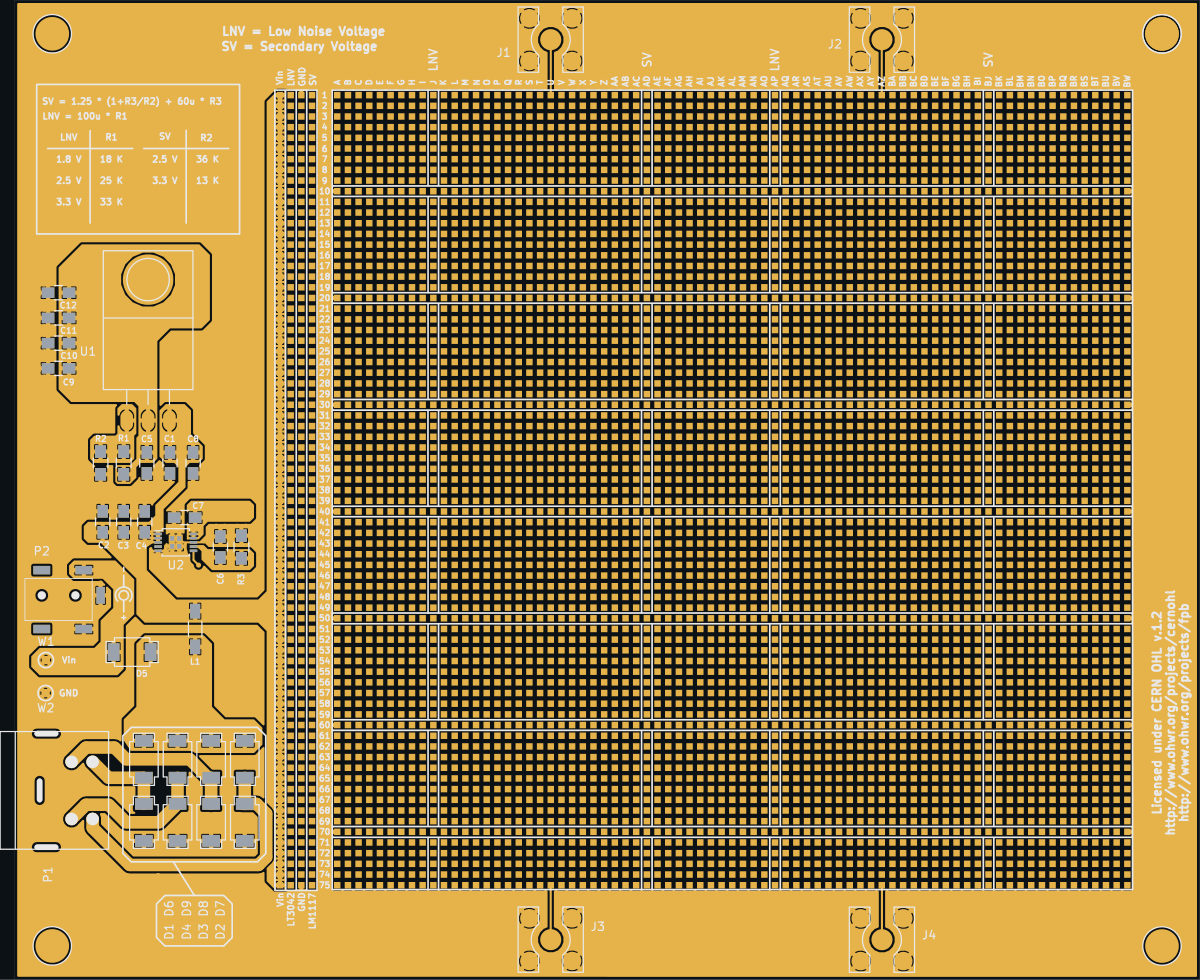
R19 TDC DEL A FILTER (OHWR0066 R1) is an open-hardware circuit board from the CERN Open Hardware Repository, designed in KiCad EDA: a 4-layer board of 141 × 116.5 mm with 6140 components and 18 nets, published under CERN-OHL-1.2.
review 91% walked · 10 findings: 1 blocker · 5 major · 4 minor
Open in the interactive viewerRead the full review
Design review
Probe recorded 10 findings: 1 blocker · 5 major · 4 minor on this design. Each is shown here with its reasoning; the full review links every one to the pins, nets and datasheet pages it rests on.
- CopperShortBetweenNetsblockerOpen
GND and P5V0 copper touch on B.CU, at (91.15, -101.56): the two nets are shorted in the copper as exported
GND and P5V0 copper touch on B.CU, at (91.15, -101.56): the two nets are shorted in the copper as exported. Where: B.CU at (91.15, -101.56) (one net's copper edge lies in the other's copper). The netlist still puts the two nets apart, so every connectivity check passes; the copper the fab builds joins them. The usual cause is a pour filled before the other net's via or pad was placed (or moved), so it runs through it without a clearance: refill the zones, check the CAD tool's DRC is clean, and export again. copper-near at a site shows both nets' copper at distance 0.
At short:GND|P5V0
LM1117 U1 output stability: only 4.7 uF ceramics on its output, datasheet requires a minimum 10 uF tantalum
The LM1117 U1 output (P3V3) has only 4.7 µF ceramics, while the datasheet requires a minimum 10 µF tantalum for stability.
The numbers
Quantity Value Source Capacitors on P3V3 C5, C9, C10, C11, C12, each 4u7 on footprint C_0805_HandSoldering (ceramic by footprint); no MPN or dielectric in the BOM netlist: P3V3; BOM LM1117 output requirement 'A minimum of 10-µF tantalum capacitor is required', to improve transient response and stability LM1117 datasheet, p.1 Why it matters
The LM1117 is an older NPN-pass LDO whose stability relies on the output capacitor's ESR, which a ceramic does not provide. Five 4.7 µF ceramics give enough capacitance but near-zero ESR, and the LM1117 family is known to oscillate with low-ESR output capacitance alone.
Suggested fix: fit a 10 µF tantalum on P3V3, or add series resistance per the datasheet's output-capacitor section.
LM1117-ADJ U1 has no minimum load: its 13k/13k feedback divider draws about 0.1 mA against a 5 mA minimum load current
The LM1117-ADJ U1 on P3V3 has no minimum load: its 13k/13k feedback divider draws about 96 µA, against a minimum load current of 1.7 mA typical and 5 mA maximum, so with nothing fitted on the pad matrix the output is not guaranteed to stay in regulation.
The numbers
Quantity Value Source Feedback divider R1 13k (P3V3 / U1 VOUT to ADJ), R2 13k (ADJ to GND); no other resistor loads P3V3 netlist: Net-(R1-Pad2); BOM P3V3, typical 1.25 V × (1 + 13k/13k) + 60 µA × 13k ≈ 3.28 V LM1117 datasheet p.11 (Fig. 8-1), p.5, p.6 Divider current (through R1) VREF / R1 = 1.25 V / 13 kΩ = 96 µA derived LM1117-ADJ minimum load current 1.7 mA typical at 25 °C, 5 mA maximum over 0 °C to 125 °C ('the minimum output current required to maintain regulation') LM1117 datasheet p.6 Usual R1 (output to adjust) 'normally in the range of 100 Ω to 200 Ω', which provides that load LM1117 datasheet p.15 The divider current is set by VREF across R1 alone, so this holds whatever the output voltage is; it does not depend on the P3V3 value.
Why it matters
The pad-matrix board is often powered with nothing fitted on P3V3, which is exactly the no-load case: the regulator then runs 50× below its guaranteed minimum load, and the output can rise out of regulation.
Options:
- scale the divider down: for 3.3 V, R1 = 124 Ω and R2 = 205 Ω gives 1.25 × (1 + 205/124) + 60 µA × 205 Ω ≈ 3.33 V and draws about 10 mA; this also makes the output nearly independent of the adjust-pin current, which with 13k in R2 contributes 0.78 V typical
- or add a bleed resistor on P3V3 that draws at least 5 mA (for example 620 Ω at 3.3 V ≈ 5.3 mA)
A GND via overlaps the P5V0 track on B.CU at (91.15, -101.56): 5 V shorted to ground in the exported copper
On B.CU at (91.15, -101.56) mm, a GND stitching via sits on the edge of the wide P5V0 track and its land overlaps the track, so P5V0 is shorted to GND in the copper as exported.
The piece image of the site (B.CU, 88.7-93.7 x -104.1 to -99.1 mm, seen from the bottom) shows the via land inside the track's clearance and overlapping the track edge. The neighbouring GND vias keep their clearance.
If the fabricated board matches this export, the 5 V rail is shorted at power-up. A DRC after zone refill should flag this. Moving the via clears it.
- PartLifecyclemajorOpen
5-1814400-1 on 4 placements (J1, J2, J3, J4): the distributor catalogue reports "Obsolete" for TE Connectivity AMP Connectors's 5-1814400-1
5-1814400-1 on 4 placements (J1, J2, J3, J4): the distributor catalogue reports "Obsolete" for TE Connectivity AMP Connectors's 5-1814400-1 — a sourcing/longevity risk to confirm against the MANUFACTURER before acting. This board's BOM names no manufacturer for it, so whether that is the fitted maker's product was not checked. A distributor delisting is not the same claim as the part being unavailable; check the vendor's own lifecycle/product-change notice for the status and any named successor. Re-read the source: GET /api/odb/parts/5-1814400-1/providers (which provider said it, the maker and part number it matched, its own words, and when we asked). THE LAST BUY DATE HAS PASSED (2020-03-01, 2,450 day(s) ago), so this is a substitution rather than a buy. The distributor reports NONE left. No approved alternate is recorded for this position.
At J1
- FiducialMissingmajorOpen
The top side carries 16 SMT component(s) and no fiducial was found on it
The top side carries 16 SMT component(s) but no fiducial was found on it — a placement machine has no optical reference to align to. Probe found no pad labelled .pad_usage=g_fiducial/l_fiducial (basis pad_usage); no single-pad, netless, undrilled component whose 0.5-3 mm round pad has a concentric solder-mask opening at least 1.5x its diameter with no other copper inside it (basis geometry); and no component whose refdes starts FID or whose part or package name contains FIDUCIAL (basis footprint-name). If your library names fiducials something Probe does not recognise, mark this benign — disposition_finding(rule='FiducialMissing', entity='top', status='benign', reason=…) — the name match only ever silences this check, it never asserts anything. If the side really has no fiducial, say so with status='confirmed': that answers the finding and keeps it gating release.
At top
LT3042 U2 output capacitor C7 is 4.7 uF nominal, exactly the datasheet minimum, with no DC-bias or tolerance margin
The LT3042 U2 output capacitor C7 is 4.7 µF nominal, exactly the datasheet minimum, so DC bias and tolerance put the effective value below it.
The numbers
Quantity Value Source Capacitance on P1V8 (U2 OUT pin 10, OUTS pin 9) C7 = 4u7, 0805 (C_0805_HandSoldering), the only capacitor; no MPN or dielectric in the BOM netlist: P1V8; BOM LT3042 minimum output capacitor 4.7 µF ceramic LT3042 datasheet, p.1 0805 MLCC tolerance -10 to -20 %, plus loss with DC bias statement The same pattern is recorded on the sister ADC board as OBS-117.
Why it matters
Below the minimum the LT3042 loses phase margin, and its noise and PSRR figures no longer hold. That matters on a board meant for prototyping low-noise filters.
Suggested fix: fit 10 µF (or two 4.7 µF) on P1V8.
The nine SOD-128 Schottky diodes D1 to D9 carry no cathode mark on the top silkscreen
The nine SOD-128 Schottky diodes D1 to D9 have no cathode mark on the top silkscreen, on a hand-assembled board where a reversed bridge diode shorts the input.
Where it is
- D1 to D9 are PMEG3050EP (SOD-128): D5 is the input reverse-polarity diode, and D1-D4/D6-D9 form the double bridge.
- On the top silkscreen (F.SILKS, input region x 60-110, y -160 to -75) each diode is a plain two-pad outline with no bar, dot or triangle marking the cathode.
- The bridge diodes are named only in a grouped legend box: 'D1 D6 / D4 D9 / D3 D8 / D2 D7'.
The same omission is recorded on the sister ADC board as OBS-118.
Why it matters
This board is hand-assembled (HandSoldering footprints, THT regulator), and a reversed diode in the bridge shorts the input on one polarity.
Suggested fix: add a cathode bar to the SOD-128 footprint silk.
Sheet note allows 20 V input, but the LM1117 U1 on that input is rated 15 V operating (20 V absolute maximum)
The sheet note allows a 20 V input, but the LM1117 U1 fed from that input is rated 15 V maximum operating and 20 V absolute maximum, so the documented range takes it past its operating limit and up to its absolute maximum.
The numbers
Quantity Value Source Documented input 'Maximum Vin = + 20 V, Minimum Vin = + 2 V (if LM1117 not used)' schematic sheet 1, note near P2 U1 VIN (pin 3) on P5V0, the rectified input after D5 or the D1-D9 bridge and ferrite L1, with no other regulator in front netlist; schematic sheet 1 LM1117 recommended input, maximum 15 V LM1117 datasheet p.4 LM1117 absolute maximum input 20 V LM1117 datasheet p.4 U1 output (P3V3), typical 1.25 V × (1 + 13k/13k) + 60 µA × 13k ≈ 3.28 V LM1117 datasheet p.11 (Fig. 8-1), p.5, p.6; BOM R1 = R2 = 13k Dissipation at 20 V in, 3.28 V out (20 − 3.28) V × 10 mA ≈ 167 mW per 10 mA of load, in the TO-220 with no heatsink shown derived Why it matters
Between 15 V and 20 V the LM1117 is outside its recommended operating conditions, and at 20 V there is no margin at all to the absolute maximum rating. The input diode drop helps a little but is not a design margin.
Options: limit the documented input to 15 V (the LT3042 U2 on the same rail is fine to 20 V, 22 V absolute), or note that U1 must be removed above 15 V.
The note already says the 2 V minimum applies 'if LM1117 not used', so the author considered the LM1117 optional; the maximum needs the same caveat.
LM1117-ADJ U1: P3V3 rests on the adjust-pin current; 13k in R2 lets it range from 3.28 V typical to about 4.1 V at the datasheet's 120 uA maximum
P3V3 on the LM1117-ADJ U1 is set mostly by the regulator's adjust-pin current, not by its divider: with R2 = 13 kΩ the 60 µA typical IADJ supplies 0.78 V of the 3.28 V, and the datasheet's 120 µA maximum takes the rail to about 4.1 V, so the '3.3 V' row of the pad matrix is only 3.3 V for a typical part.
Where it is
U1 LM1117T-ADJ/NOPB: VOUT (pin 2) on P3V3, ADJ (pin 1) on Net-(R1-Pad2), VIN (pin 3) on P5V0. R1 13k runs from P3V3 to ADJ and R2 13k from ADJ to GND, the same positions as R1 and R2 in the datasheet's Figure 8-1. The sheet states 'The default configuration gives 3.3V (from the LM1117)' and uses the formula 'Vout = 1.25 * (1+R3/R2) + 60u * R3', so it relies on the typical 60 µA.
The numbers
Quantity Value Source Output equation VOUT = VREF × (1 + R2/R1) + IADJ × R2 LM1117 datasheet p.11, Figure 8-1 R1 (VOUT to ADJ), R2 (ADJ to GND) 13 kΩ, 13 kΩ; tolerance not stated in the BOM, so not included below BOM; netlist Net-(R1-Pad2) VREF 1.238 / 1.25 / 1.262 V at 25 °C; 1.225 V to 1.27 V over 0 °C to 125 °C (10 mA ≤ IOUT ≤ 800 mA) LM1117 datasheet p.5 IADJ 60 µA typical at 25 °C; 120 µA maximum over 0 °C to 125 °C; no minimum given LM1117 datasheet p.6 IADJ change with load and line 0.2 µA typical at 25 °C; 5 µA maximum over 0 °C to 125 °C (10 mA ≤ IOUT ≤ 800 mA, 1.4 V ≤ VIN − VOUT ≤ 10 V) LM1117 datasheet p.6 Divider term VREF × (1 + 13k/13k) 2 × VREF = 2.45 V min, 2.50 V typ, 2.54 V max derived IADJ term IADJ × 13 kΩ 0.78 V typical (24 % of the output); 1.56 V at 120 µA derived P3V3, typical 2.50 + 0.78 = 3.28 V derived P3V3, upper bound 2.54 + 1.56 = 4.10 V (2.50 + 1.56 = 4.06 V at typical VREF) derived P3V3, lower bound the datasheet gives no IADJ minimum, so the only bound it supports is IADJ → 0: 2 × 1.225 = 2.45 V derived P3V3 at typical IADJ, VREF limits 2.45 + 0.78 = 3.23 V to 2.54 + 0.78 = 3.32 V derived Shift with load / line 5 µA × 13 kΩ = 65 mV worst case (0.2 µA × 13 kΩ = 2.6 mV typical) derived Same term with the datasheet's resistor class R1 'normally in the range of 100 Ω to 200 Ω'; with R1 = 124 Ω and R2 ≈ 205 Ω for 3.3 V, 120 µA × 205 Ω ≈ 25 mV LM1117 datasheet p.15; derived The datasheet explains why the term is normally ignored: IADJ 'is very small (60 µA) compared to the I1' (p.11). Here I1 = VREF / R1 = 1.25 V / 13 kΩ ≈ 96 µA, the same order as IADJ, so that assumption does not hold.
What P3V3 feeds
On this board P3V3 reaches only U1 VOUT, R1, the output capacitors C5, C9, C10, C11, C12 and 231 single-pad footprints of the prototyping pad matrix, none of which is a BOM part (netlist, net P3V3). No fitted device takes its supply from P3V3, so no fitted part is exposed and there is no load datasheet on file to compare against. The exposure is whatever a user builds on the matrix against the '3.3 V' row, which the documents on file cannot bound.
At the upper end the regulator may also run out of headroom: with P5V0 at 5 V, VIN − VOUT at 4.06 V out is 0.94 V, below the 1.1 V to 1.3 V dropout on p.6, so the rail would then follow the input rather than the divider. P5V0 comes from the external input through diodes, so its actual level is not fixed by the design.
Relation to other observations
- OBS-112 (refuted) claimed 2.5 V from an arithmetic slip; its refutation confirms 3.28 V typical and names this spread as a separate question. This observation is that question.
- OBS-470 is the minimum-load problem of the same divider and OBS-471 the 20 V input note. Neither is about output accuracy.
- Scaling the divider down, as OBS-470 suggests (for example R1 = 124 Ω, R2 = 205 Ω), also removes this spread: the IADJ term falls from 0.78 V to about 12 mV typical.
Main parts
| Part number | Maker | Description | Where |
|---|---|---|---|
| LM1117T-ADJ/NOPB | U1 | ||
| LT3042EMSE#PBF | U2 | ||
| PJ-075DH-SMT-TR | P2 | ||
| 5-1814400-1 | J1, J2, J3, J4 | ||
| PMEG3050EP | Schematic note: 'All Schottky diodes are NXP PMEG3050EP' (BOM value D_Schottky); MPN added by Claude walker (Cern session) | D1, D2, D3, D4, D5, D6 and 3 more | |
| BLM41PG181SN1 | Ferrite bead Murata BLM41PG181SN1 | L1 |
About this design
- Design
- R19 TDC DEL A FILTER — OHWR0066 R1
- Designed in
- KiCad EDA
- Board
- 4 copper layers, 141 × 116.5 mm, 6140 components, 18 nets
- Licence
- CERN-OHL-1.2
- Source
- https://gitlab.com/ohwr/project/r19-tdc-del-a at commit
3fa327631793 - Attribution
- CERN Open Hardware Repository, project ohwr/project/r19-tdc-del-a (commit 3fa327631793eebdf42d263f79ed5e8637f62ac9, 2025-04-12). Licence: CERN-OHL-1.2. Source: https://gitlab.com/ohwr/project/r19-tdc-del-a. This is a snapshot of the copy published on the OHWR GitLab pages (R1), not CERN's released record. CERN's source of truth is EDMS (https://edms.cern.ch), and the current release may be newer.
- Reviewed with
- Probe by E# (E-Sharp AB)