 Probe

RATOPUS DCDC STAGE
OHWR0088 · revision R5
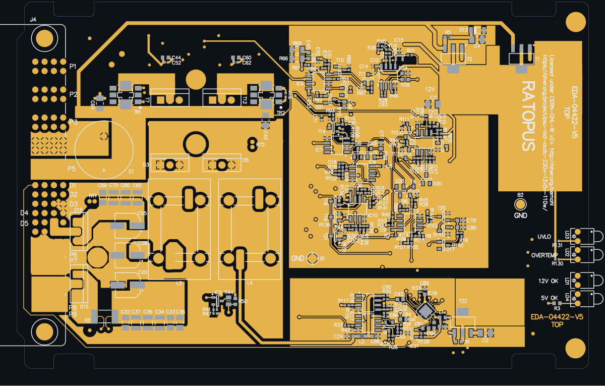
RATOPUS DCDC STAGE (OHWR0088 R5) is an open-hardware circuit board from its public repository, designed in Altium Designer: a 4-layer board of 156 × 100 mm with 294 components and 130 nets, published under CERN-OHL-W-2.0.
review 86% walked · 14 findings: 1 blocker · 6 major · 7 minor (31 items)
Open in the interactive viewerRead the full review
Design review
Probe recorded 14 findings: 1 blocker · 6 major · 7 minor (31 items) on this design. Each is shown here with its reasoning; the full review links every one to the pins, nets and datasheet pages it rests on.
- NetCopperSplitblockerOpen
NetCopperSplit: 3 boards×3
Refuted once, awaiting a second check · Claude walker W2 (Cern session)
At split:NetC5_2, split:NetC6_2, split:P5V
Each finding, with its own headline
split:NetC5_2NetC5_2's copper is in 2 pieces: L3.1 is not connected to the rest of the net
NetC5_2's copper is in 2 pieces: L3.1 is not connected to the rest of the net. Piece 1: C23.2, C5.2, D3.2, IC8.6, R22.1 and T7.3, on TOP_LAYER, L3 and BOTTOM_LAYER, 3 drill(s), over (111.78, 119.71) to (124.2, 160.85). Piece 2: L3.1, on TOP_LAYER, over (122, 119.71) to (124.2, 125.21). The export files every one of these pins under the net, so every connectivity check passes; the copper the fab builds leaves them apart. Usually a pour island that touches only one via of its own net, or a track ending short of its copper: join the piece to the net and export again.
split:NetC6_2NetC6_2's copper is in 2 pieces: L4.1 is not connected to the rest of the net
NetC6_2's copper is in 2 pieces: L4.1 is not connected to the rest of the net. Piece 1: C58.2, C6.2, D5.2, IC9.6, R67.1 and T12.3, on TOP_LAYER, L3 and BOTTOM_LAYER, 3 drill(s), over (130.98, 119.71) to (143.4, 160.85). Piece 2: L4.1, on TOP_LAYER, over (141.2, 119.71) to (143.4, 125.21). The export files every one of these pins under the net, so every connectivity check passes; the copper the fab builds leaves them apart. Usually a pour island that touches only one via of its own net, or a track ending short of its copper: join the piece to the net and export again.
split:P5VP5V's copper is in 3 pieces: D14.2, R3.2, R49.1 and R97.1 and 1 other piece(s) are not connected to the rest of the net
P5V's copper is in 3 pieces: D14.2, R3.2, R49.1 and R97.1 and 1 other piece(s) are not connected to the rest of the net. Piece 1: C43.1, C55.1, C65.1, C66.1, C67.1, C68.1, C69.2, C70.1 and 5 more pin(s), on TOP_LAYER, L3 and BOTTOM_LAYER, 16 drill(s), 356.31 mm2 of pour, over (91.36, 103.11) to (138.28, 122.71). Piece 2: D14.2, R3.2, R49.1 and R97.1, on TOP_LAYER, L3 and BOTTOM_LAYER, 5 drill(s), over (135.97, 93.51) to (223.2, 131.73). Piece 3: C24.2, L2.1 and L4.2, on TOP_LAYER, over (135.97, 82.8) to (169.98, 108.7). The export files every one of these pins under the net, so every connectivity check passes; the copper the fab builds leaves them apart. Usually a pour island that touches only one via of its own net, or a track ending short of its copper: join the piece to the net and export again.
AD8512 op-amps run single-supply with inputs below their guaranteed input range; IC18 runs at 5.3 V, under the specified supply
The AD8512 JFET op-amps (IC1, IC2, IC6, IC10, IC14, IC17, IC18) run from a single supply with GND as V-, and most of their inputs sit 1-2.5 V above GND, below the input range the datasheet guarantees. IC18 also runs from 5.3 V, under the specified supply range. The 12 V and 5 V error amplifiers and the monitoring buffers therefore work only on typical behaviour.
What the datasheet guarantees
Specification Value Source Supply "Dual-supply operation: ±5 V to ±15 V"; PSRR specified over ±4.5 V to ±18 V (9 V total minimum) AD8510/12/13 Rev. H, p.1 and p.3 Input voltage range at ±5 V -2.0 V to +2.5 V, i.e. from V- + 3.0 V to V+ - 2.5 V p.3 Input voltage range at ±15 V -13.5 V to +13.0 V, i.e. from V- + 1.5 V to V+ - 2.0 V p.4 What the board asks
Amplifier Supply (V- = GND) Inputs Source IC1B, 12 V error amp B10V, about 12.3 V 2.5 V (IC15 reference) sheet 2 IC6A, 5 V error amp B10V 2.5 V (IC22 reference) sheet 4 IC1A, P12V sense B10V P12V x 2.2k / 12.7k = about 2.1 V sheet 2 IC2A / IC14A, OCP / OVP comparators B10V about 0.74 V / about 1.0-1.2 V sheet 6 IC17A, M_12V buffer B10V P12V x 2k / 12k = about 2.0 V sheet 8 IC17B, 12 V current sense B10V, about 12.3 V CSENSE_12V+/- at about 12.3 V, above V+ - 2 V sheet 8 IC18A/B, M_5V and M_I5V buffers P5VA, 5.3 V single, below the 9 V minimum about 2.0 V sheet 8 Why it matters
A JFET-input amplifier with inputs below its specified common-mode range can lose gain and offset accuracy and, at temperature extremes, saturate. The board's 12 V and 5 V output regulation (IC1B, IC6A) and its over-current, over-voltage and under-voltage thresholds depend on these amplifiers. IC18 runs outside its rated supply, so the AD7291's 5 V voltage and current readings (M_5V, M_I5V) have no datasheet basis. A rail-to-rail-input single-supply op-amp, or a negative rail for the AD8512s, would put every input inside a guaranteed range.
In the crate, the management I2C and P_RST arrive at 3.3 V from the system board, above this AD7291's VDRIVE + 0.3 V (about 3.2 V) input limit
In the DI/OT crate (OHWR-DIOT-CRATE-V3 build 2), the system board OHWR0083 R5 DIOT SB ZU pulls the management I2C (M_SCL/M_SDA) up to its 3.3 V rail and drives P_RST from a 3.3 V FPGA bank, while this board's AD7291 (IC16) runs its digital I/O from VDRIVE = P3V3 at about 2.9 V. Every high level on SDA, SCL and PD/RST therefore sits above the AD7291's absolute maximum of VDRIVE + 0.3 V.
This confirms with the assembled crate what [OBS-587] could only anticipate on this board alone ("a pull-up to 3.3 V elsewhere in the crate would sit at or above that limit").
The path
``
mermaid graph LR SB["SB ZU R5: IC52 MIO62/63 (bank 502, 3.3 V), R329/R368 4k7 to P3V3, IC42 LTC4311 on P3V3"] -->|M_SCL / M_SDA| BP["Main backplane J2 A7/B7"] SB2["SB ZU R5: IC52.E6 (HD bank 93, 3.3 V) via R264 22R"] -->|P_RST| BP BP --> FI["Front Interface J3 / J2"] --> PBP["Power backplane J4 → J1/J2 A1, A5, B5"] PBP --> AD["This board: IC16 AD7291 SCL 15, SDA 14, PD/RST 17 (VDRIVE 16 = P3V3, 2.9 V)"]``The numbers
Quantity Value Source I2C high level 3.3 V: 4.7 k pull-ups (R329, R368) and the LTC4311 accelerator (IC42) all on the system board's P3V3 OHWR0083 R5 netlist P_RST high level 3.3 V push-pull: IC52.E6, HD bank 93, VCCO = P3V3, no pull resistor OHWR0083 R5 netlist and IC52 bank map VDRIVE on this board P3V3 = about 2.9 V (Zener D13 BZV55-B3V6 + emitter follower T22 BCP56) netlist; [OBS-587] AD7291 digital input limit −0.3 V to VDRIVE + 0.3 V, i.e. about 3.2 V here AD7291 Rev. C, Table 4, p.6 Margin 3.3 V − 3.2 V = 0.1 V over, more with the system board's 3.3 V at its upper tolerance or a low Zener derived Why it matters
- The excess forward-biases the AD7291's input protection on every high bit and every idle-high bus period, both PSU slots at once (PSU0 and PSU1 share the bus and P_RST).
- The injected current has nowhere to go but P3V3, which is an emitter follower: it can source but not sink, so the injection lifts the AD7291's own supply. R33 (2 k, ADC_RST_N to P3V3) adds a further path from the 3.3 V-driven P_RST into the same rail.
- Raising this board's P3V3 to 3.3 V (the fix proposed in [OBS-587]) removes the overstress. Otherwise an I2C level translator and a series resistor or divider on P_RST would.
- AssemblySeammajorOpen
AssemblySeam: 2 nets×2
e.g. “Nothing sources DC_RTN1 (OHWR-DIOT-CRATE-V3)” · 2 different statements
At P24V
Each finding, with its own headline
P24VNothing sources DC_RTN1 (OHWR-DIOT-CRATE-V3)
Every board this rail reaches receives it (PBP DC_RTN1, ACDC0 VRECT, PSU0 P24V), no declared member sources it, and it leaves the build through no other connector.
Found by the seam review of OHWR-DIOT-CRATE-V3 build 2 (M9-rail-direction, across seam:16, seam:18), where this board sits as PSU0. On the assembly it is STALE: decided refuted by Claude interconnect reviewer (Cern session): Refuted for the real crate. DC_RTN1 carries VRECT (+24 V) of the RaToPUSv2 AC/DC stage seated as ACDC0, produced on that board by the D1 (DST2080C) / D2 (DSTF3060CR) full-wave bridge from the 2x 18 V secondaries of its off-board toroid TR1 (Multicomp MCTA160/18), which enter on its J3 (CERN schematic EDA-04862-V2-0 sheet 1). The transformer is now seated as declared member TR0 (supply, no copper). No MCTA160/18 datasheet or pinout is on file, so no connection diagram is declared and the engine cannot see it source; in addition the bridge rule does not admit VRECT (CERN BUG-072). The polarity of this feed against spec Table 3 is raised separately in OBS-581.
P24VNothing sources DC_RTN2 (OHWR-DIOT-CRATE-V3)
Every board this rail reaches receives it (PBP DC_RTN2, ACDC1 VRECT, PSU1 P24V), no declared member sources it, and it leaves the build through no other connector.
Found by the seam review of OHWR-DIOT-CRATE-V3 build 2 (M9-rail-direction, across seam:17, seam:19), where this board sits as PSU1. On the assembly it is STALE: decided refuted by Claude interconnect reviewer (Cern session): Refuted for the real crate. DC_RTN2 carries VRECT (+24 V) of the RaToPUSv2 AC/DC stage seated as ACDC1, produced on that board by the D1 (DST2080C) / D2 (DSTF3060CR) full-wave bridge from the 2x 18 V secondaries of its off-board toroid TR1 (Multicomp MCTA160/18), which enter on its J3 (CERN schematic EDA-04862-V2-0 sheet 1). The transformer is now seated as declared member TR1 (supply, no copper). No MCTA160/18 datasheet or pinout is on file, so no connection diagram is declared and the engine cannot see it source; in addition the bridge rule does not admit VRECT (CERN BUG-072). The polarity of this feed against spec Table 3 is raised separately in OBS-581.
- BomLayoutMismatchmajorOpen
BomLayoutMismatch: 2 components×2
Checked by the review, stands · Claude walker C (Cern session) — Checked: NT1 and NT2 are Altium Net Tie footprints (sheet 3 'NetTie' symbols on CSENSE_12V+ and CSENSE_12V- at the R2 shunt), copper bridges that keep the Kelvin sense nets separate from P12V/P12V_OUT. A net tie is not an assembled part, so CERN's BOM correctly has no line for it. The disagreement is real but expected; left for the owner.
At NT1, NT2
Each finding, with its own headline
- NT1'NT1' is placed in the layout but absent from the BOM.
- NT2'NT2' is placed in the layout but absent from the BOM.
- PartLifecyclemajorOpen
PartLifecycle: 2 part numbers×2
2 Obsolete · on 9 placements
At D7, IC1
Each finding, with its own headline
D7BAT54C on 2 placements (D7, D8): the distributor catalogue reports "Obsolete" for onsemi's BAT54C
BAT54C on 2 placements (D7, D8): the distributor catalogue reports "Obsolete" for onsemi's BAT54C — a sourcing/longevity risk to confirm against the MANUFACTURER before acting. This board's BOM names FAIRCHILD SEMICONDUCTOR, and that is one line with onsemi: ON Semiconductor completed its acquisition of Fairchild Semiconductor on 2016-09-19 and renamed itself onsemi on 2021-08-05. A distributor delisting is not the same claim as the part being unavailable; check the vendor's own lifecycle/product-change notice for the status and any named successor. Re-read the source: GET /api/odb/parts/BAT54C/providers (which provider said it, the maker and part number it matched, its own words, and when we asked). THE LAST BUY DATE HAS PASSED (2018-09-30, 2,968 day(s) ago), so this is a substitution rather than a buy. The distributor reports 54,983 left. No approved alternate is recorded for this position.
IC1AD8512AR on 7 placements (IC1, IC10, IC14, IC17, IC18, IC2, IC6): the distributor catalogue reports "Obsolete" for Analog Devices Inc.'s AD8512AR
AD8512AR on 7 placements (IC1, IC10, IC14, IC17, IC18, IC2, IC6): the distributor catalogue reports "Obsolete" for Analog Devices Inc.'s AD8512AR — a sourcing/longevity risk to confirm against the MANUFACTURER before acting. That is the maker this board's BOM names (ANALOG DEVICES). A distributor delisting is not the same claim as the part being unavailable; check the vendor's own lifecycle/product-change notice for the status and any named successor. Re-read the source: GET /api/odb/parts/AD8512AR/providers (which provider said it, the maker and part number it matched, its own words, and when we asked). THE LAST BUY DATE HAS PASSED (2012-10-27, 5,132 day(s) ago), so this is a substitution rather than a buy. The distributor reports NONE left. No approved alternate is recorded for this position.
- ReferencePlaneDiscontinuitymajorOpen
ReferencePlaneDiscontinuity: 9 boards×9
Checked by the review, stands · Claude walker C (Cern session) — Checked: every crossing is on a slow control or analog net of a 160-200 kHz power supply: CSENSE_12V+/- (the shunt Kelvin pair to IC17B), the PTC divider nodes NetC27_2/NetC30_2 (with 100 nF), 12V_BPSD (filtered by R145 10k / C78 10uF), NetLD1_2 (LED), MM_SCL (I2C), NetR82_2 (frequency foldback), and nets on L3 crossing tracks routed through the bottom GND pour. None carries a fast edge for which a return-path detour matters at these frequencies; the long CSENSE crossing is a differential low-frequency sense pair. Not refutable with a citation; left for the owner.
At void:GND@BOTTOM_LAYER:149.55,129.47, void:GND@BOTTOM_LAYER:149.55,132.67, void:GND@BOTTOM_LAYER:149.68,99.76, void:GND@BOTTOM_LAYER:hole 154.48,113.47|158.83,131.93, void:GND@BOTTOM_LAYER:hole 155.73,111.67|156.99,126.52, void:GND@BOTTOM_LAYER:hole 156.49,152.88|159.95,156.35 and 3 more
Each finding, with its own headline
void:GND@BOTTOM_LAYER:149.55,129.47'NetC30_2' crosses where the outline of the GND plane on BOTTOM_LAYER is drawn back, at 1 place, the longest 2.42 mm (fastest: NetC30_2 at 100 ps 10-90 %, ASSUMED)
Along 'NetC30_2' on L3, the GND plane on BOTTOM_LAYER has 2.42 mm under the track with no copper, at (149.55, 129.47), the same plane on both sides. No single drill's anti-pad and no landing explains it: a clearance is excused only when it holds a drill and is drawn round it, or the track ends in it on the net's own pad or via, or runs through its own via's clearance and no farther. The return current detours round the void. No hole cleared it: the outline of the pour at x 80.3..206.56, y 81.86..170.65 is drawn back there. One decision covers the void: whether these tracks may cross it, or the plane should be filled under them. 0 of the 1 crossing(s) have a plane on the track's other side at most twice as far away as the broken one (to first order each plane beside a stripline carries a share of the return inversely proportional to its distance from the track). The rest leave most or all of the return to the break, so the finding is a warning.
- 'NetC30_2' on L3 at (149.55, 129.47), 2.42 mm over no copper; other side: GND on L2-GND, 0.92 mm from the track against 0.25 mm to BOTTOM_LAYER: 79% of the return on BOTTOM_LAYER
Every site is a row of this finding's evidence, keyed by net, layers and position. GET /api/odb/boards/92/reference-planes?group=void%3AGND%40BOTTOM_LAYER%3A149.55%2C129.47 serves each with its own layer_image region; all of them lie in x 147.69..151.4, y 127.61..131.32 mm (board frame, Y up).
Read from the copper as drawn on the reference layer, along each track's centreline at exact breakpoints. The reference is the copper beside the track, never the layer's type or name. Whether it matters depends on each signal's edge rate, which nothing on file states for these nets: a slow static line crosses a split harmlessly, a fast edge does not.
void:GND@BOTTOM_LAYER:149.55,132.67'NetC27_2' crosses where the outline of the GND plane on BOTTOM_LAYER is drawn back, at 1 place, the longest 2.42 mm (fastest: NetC27_2 at 100 ps 10-90 %, ASSUMED)
Along 'NetC27_2' on L3, the GND plane on BOTTOM_LAYER has 2.42 mm under the track with no copper, at (149.55, 132.67), the same plane on both sides. No single drill's anti-pad and no landing explains it: a clearance is excused only when it holds a drill and is drawn round it, or the track ends in it on the net's own pad or via, or runs through its own via's clearance and no farther. The return current detours round the void. No hole cleared it: the outline of the pour at x 80.3..206.56, y 81.86..170.65 is drawn back there. One decision covers the void: whether these tracks may cross it, or the plane should be filled under them. 0 of the 1 crossing(s) have a plane on the track's other side at most twice as far away as the broken one (to first order each plane beside a stripline carries a share of the return inversely proportional to its distance from the track). The rest leave most or all of the return to the break, so the finding is a warning.
- 'NetC27_2' on L3 at (149.55, 132.67), 2.42 mm over no copper; other side: GND on L2-GND, 0.92 mm from the track against 0.25 mm to BOTTOM_LAYER: 79% of the return on BOTTOM_LAYER
Every site is a row of this finding's evidence, keyed by net, layers and position. GET /api/odb/boards/92/reference-planes?group=void%3AGND%40BOTTOM_LAYER%3A149.55%2C132.67 serves each with its own layer_image region; all of them lie in x 147.69..151.4, y 130.82..134.53 mm (board frame, Y up).
Read from the copper as drawn on the reference layer, along each track's centreline at exact breakpoints. The reference is the copper beside the track, never the layer's type or name. Whether it matters depends on each signal's edge rate, which nothing on file states for these nets: a slow static line crosses a split harmlessly, a fast edge does not.
void:GND@BOTTOM_LAYER:149.68,99.76'NetLD1_2' crosses where the outline of the GND plane on BOTTOM_LAYER is drawn back, at 1 place, the longest 2.8 mm (fastest: NetLD1_2 at 100 ps 10-90 %, ASSUMED)
Along 'NetLD1_2' on L3, the GND plane on BOTTOM_LAYER has 2.8 mm under the track with no copper, at (149.68, 99.76), the same plane on both sides. No single drill's anti-pad and no landing explains it: a clearance is excused only when it holds a drill and is drawn round it, or the track ends in it on the net's own pad or via, or runs through its own via's clearance and no farther. The return current detours round the void. No hole cleared it: the outline of the pour at x 80.3..206.56, y 81.86..170.65 is drawn back there. One decision covers the void: whether these tracks may cross it, or the plane should be filled under them. 0 of the 1 crossing(s) have a plane on the track's other side at most twice as far away as the broken one (to first order each plane beside a stripline carries a share of the return inversely proportional to its distance from the track). The rest leave most or all of the return to the break, so the finding is a warning.
- 'NetLD1_2' on L3 at (149.68, 99.76), 2.8 mm over no copper; other side: GND on L2-GND, 0.92 mm from the track against 0.25 mm to BOTTOM_LAYER: 79% of the return on BOTTOM_LAYER
Every site is a row of this finding's evidence, keyed by net, layers and position. GET /api/odb/boards/92/reference-planes?group=void%3AGND%40BOTTOM_LAYER%3A149.68%2C99.76 serves each with its own layer_image region; all of them lie in x 147.69..151.67, y 97.77..101.75 mm (board frame, Y up).
Read from the copper as drawn on the reference layer, along each track's centreline at exact breakpoints. The reference is the copper beside the track, never the layer's type or name. Whether it matters depends on each signal's edge rate, which nothing on file states for these nets: a slow static line crosses a split harmlessly, a fast edge does not.
void:GND@BOTTOM_LAYER:hole 154.48,113.47|158.83,131.933 nets cross one void in the GND plane on BOTTOM_LAYER at 3 places, the longest 2.51 mm; 3 over tracks of other nets routed inside it (fastest: NetC27_2 at 100 ps 10-90 %, ASSUMED)
Along 'NetC27_2' on L3, the GND plane on BOTTOM_LAYER has 2.51 mm under the track with copper of P5V, not a plane, at (154.94, 126.53), the same plane on both sides. No single drill's anti-pad and no landing explains it: a clearance is excused only when it holds a drill and is drawn round it, or the track ends in it on the net's own pad or via, or runs through its own via's clearance and no farther. The return current detours round the void. 3 of the crossings pass over tracks of other nets routed inside the hole on the reference layer: the plane is absent there, and those tracks stand in it. 1 of them run ALONG the bare copper, parallel to its edges, rather than across it (the longest 1.5 mm). 3 places on 3 net(s) cross it, listed below, the longest first. What cleared it: the hole at x 154.48..158.83, y 113.47..131.93. One decision covers the void: whether these tracks may cross it, or the plane should be filled under them. 0 of the 3 crossing(s) have a plane on the track's other side at most twice as far away as the broken one (to first order each plane beside a stripline carries a share of the return inversely proportional to its distance from the track). The rest leave most or all of the return to the break, so the finding is a warning.
- 'NetC27_2' on L3 at (154.94, 126.53), 2.51 mm, running ALONG the bare copper for 1.5 mm, not across it over copper of P5V, not a plane; other side: GND on L2-GND, 0.92 mm from the track against 0.25 mm to BOTTOM_LAYER: 79% of the return on BOTTOM_LAYER
- 'NetC30_2' on L3 at (155.08, 123.93), 1.02 mm over copper of P5V, not a plane; other side: GND on L2-GND, 0.92 mm from the track against 0.25 mm to BOTTOM_LAYER: 79% of the return on BOTTOM_LAYER
- '12V_BPSD' on L3 at (155.26, 128.36), 0.72 mm over copper of P5V, not a plane; other side: GND on L2-GND, 0.92 mm from the track against 0.25 mm to BOTTOM_LAYER: 79% of the return on BOTTOM_LAYER
Every site is a row of this finding's evidence, keyed by net, layers and position. GET /api/odb/boards/92/reference-planes?group=void%3AGND%40BOTTOM_LAYER%3Ahole%20154.48%2C113.47%7C158.83%2C131.93 serves each with its own layer_image region; all of them lie in x 153.72..156.52, y 122.57..129.62 mm (board frame, Y up).
Read from the copper as drawn on the reference layer, along each track's centreline at exact breakpoints. The reference is the copper beside the track, never the layer's type or name. Whether it matters depends on each signal's edge rate, which nothing on file states for these nets: a slow static line crosses a split harmlessly, a fast edge does not.
void:GND@BOTTOM_LAYER:hole 155.73,111.67|156.99,126.522 nets cross one void in the GND plane on BOTTOM_LAYER at 2 places, the longest 0.79 mm; 2 over tracks of other nets routed inside it (fastest: NetC27_2 at 100 ps 10-90 %, ASSUMED)
Along 'NetC27_2' on L3, the GND plane on BOTTOM_LAYER has 0.79 mm under the track with copper of 12V_BPSD, not a plane, at (156.36, 124.52), the same plane on both sides. No single drill's anti-pad and no landing explains it: a clearance is excused only when it holds a drill and is drawn round it, or the track ends in it on the net's own pad or via, or runs through its own via's clearance and no farther. The return current detours round the void. 2 of the crossings pass over tracks of other nets routed inside the hole on the reference layer: the plane is absent there, and those tracks stand in it. 2 places on 2 net(s) cross it, listed below, the longest first. What cleared it: the hole at x 155.73..156.99, y 111.67..126.52. One decision covers the void: whether these tracks may cross it, or the plane should be filled under them. 0 of the 2 crossing(s) have a plane on the track's other side at most twice as far away as the broken one (to first order each plane beside a stripline carries a share of the return inversely proportional to its distance from the track). The rest leave most or all of the return to the break, so the finding is a warning.
- 'NetC27_2' on L3 at (156.36, 124.52), 0.79 mm over copper of 12V_BPSD, not a plane; other side: GND on L2-GND, 0.92 mm from the track against 0.25 mm to BOTTOM_LAYER: 79% of the return on BOTTOM_LAYER
- 'NetC30_2' on L3 at (156.36, 123.21), 0.71 mm over copper of 12V_BPSD, not a plane; other side: GND on L2-GND, 0.92 mm from the track against 0.25 mm to BOTTOM_LAYER: 79% of the return on BOTTOM_LAYER
Every site is a row of this finding's evidence, keyed by net, layers and position. GET /api/odb/boards/92/reference-planes?group=void%3AGND%40BOTTOM_LAYER%3Ahole%20155.73%2C111.67%7C156.99%2C126.52 serves each with its own layer_image region; all of them lie in x 155..157.72, y 122.21..125.72 mm (board frame, Y up).
Read from the copper as drawn on the reference layer, along each track's centreline at exact breakpoints. The reference is the copper beside the track, never the layer's type or name. Whether it matters depends on each signal's edge rate, which nothing on file states for these nets: a slow static line crosses a split harmlessly, a fast edge does not.
void:GND@BOTTOM_LAYER:hole 156.49,152.88|159.95,156.35'NetR82_2' crosses one void in the GND plane on BOTTOM_LAYER at 1 place, the longest 1.04 mm (fastest: NetR82_2 at 100 ps 10-90 %, ASSUMED)
Along 'NetR82_2' on L3, the GND plane on BOTTOM_LAYER has 1.04 mm under the track with no copper, at (157.13, 155.05), the same plane on both sides. No single drill's anti-pad and no landing explains it: a clearance is excused only when it holds a drill and is drawn round it, or the track ends in it on the net's own pad or via, or runs through its own via's clearance and no farther. The return current detours round the void. 1 of them run ALONG the bare copper, parallel to its edges, rather than across it (the longest 0.47 mm). What cleared it: the hole at x 156.49..159.95, y 152.88..156.35. One decision covers the void: whether these tracks may cross it, or the plane should be filled under them. 0 of the 1 crossing(s) have a plane on the track's other side at most twice as far away as the broken one (to first order each plane beside a stripline carries a share of the return inversely proportional to its distance from the track). The rest leave most or all of the return to the break, so the finding is a warning.
- 'NetR82_2' on L3 at (157.13, 155.05), 1.04 mm, running ALONG the bare copper for 0.47 mm, not across it over no copper; other side: GND on L2-GND, 0.92 mm from the track against 0.25 mm to BOTTOM_LAYER: 79% of the return on BOTTOM_LAYER
Every site is a row of this finding's evidence, keyed by net, layers and position. GET /api/odb/boards/92/reference-planes?group=void%3AGND%40BOTTOM_LAYER%3Ahole%20156.49%2C152.88%7C159.95%2C156.35 serves each with its own layer_image region; all of them lie in x 155.59..158.61, y 153.99..156.05 mm (board frame, Y up).
Read from the copper as drawn on the reference layer, along each track's centreline at exact breakpoints. The reference is the copper beside the track, never the layer's type or name. Whether it matters depends on each signal's edge rate, which nothing on file states for these nets: a slow static line crosses a split harmlessly, a fast edge does not.
void:GND@BOTTOM_LAYER:hole 157.08,116.28|158.29,125.1'NetC30_2' crosses one void in the GND plane on BOTTOM_LAYER at 1 place, the longest 0.67 mm; 1 over tracks of other nets routed inside it (fastest: NetC30_2 at 100 ps 10-90 %, ASSUMED)
Along 'NetC30_2' on L3, the GND plane on BOTTOM_LAYER has 0.67 mm under the track with copper of NetC27_2, not a plane, at (157.69, 123.21), the same plane on both sides. No single drill's anti-pad and no landing explains it: a clearance is excused only when it holds a drill and is drawn round it, or the track ends in it on the net's own pad or via, or runs through its own via's clearance and no farther. The return current detours round the void. 1 of the crossings pass over tracks of other nets routed inside the hole on the reference layer: the plane is absent there, and those tracks stand in it. What cleared it: the hole at x 157.08..158.29, y 116.28..125.1. One decision covers the void: whether these tracks may cross it, or the plane should be filled under them. 0 of the 1 crossing(s) have a plane on the track's other side at most twice as far away as the broken one (to first order each plane beside a stripline carries a share of the return inversely proportional to its distance from the track). The rest leave most or all of the return to the break, so the finding is a warning.
- 'NetC30_2' on L3 at (157.69, 123.21), 0.67 mm over copper of NetC27_2, not a plane; other side: GND on L2-GND, 0.92 mm from the track against 0.25 mm to BOTTOM_LAYER: 79% of the return on BOTTOM_LAYER
Every site is a row of this finding's evidence, keyed by net, layers and position. GET /api/odb/boards/92/reference-planes?group=void%3AGND%40BOTTOM_LAYER%3Ahole%20157.08%2C116.28%7C158.29%2C125.1 serves each with its own layer_image region; all of them lie in x 156.35..159.02, y 122.21..124.21 mm (board frame, Y up).
Read from the copper as drawn on the reference layer, along each track's centreline at exact breakpoints. The reference is the copper beside the track, never the layer's type or name. Whether it matters depends on each signal's edge rate, which nothing on file states for these nets: a slow static line crosses a split harmlessly, a fast edge does not.
void:GND@BOTTOM_LAYER:relief'NetR82_2' crosses the thermal reliefs of the GND plane on BOTTOM_LAYER at 1 place, the longest 0.57 mm (fastest: NetR82_2 at 100 ps 10-90 %, ASSUMED)
The GND plane on BOTTOM_LAYER is drawn back round copper of its own net - pads spoked into it, in thermal reliefs - and tracks cross those reliefs: over the bare ring either side of the pad or spoke the return has no plane under it, and finds its way round through the spokes. 1 place(s) on 1 net(s), each the relief's bare stretches either side of that copper counted together, the longest 0.57 mm. One decision covers the pour's reliefs: whether tracks may cross them, or the reliefs or the routing should keep them apart. 0 of the 1 crossing(s) have a plane on the track's other side at most twice as far away as the broken one (to first order each plane beside a stripline carries a share of the return inversely proportional to its distance from the track). The rest leave most or all of the return to the break, so the finding is a warning.
- 'NetR82_2' on L3 at (159.48, 155.78), 0.57 mm over no copper; other side: GND on L2-GND, 0.92 mm from the track against 0.25 mm to BOTTOM_LAYER: 79% of the return on BOTTOM_LAYER
Every site is a row of this finding's evidence, keyed by net, layers and position. GET /api/odb/boards/92/reference-planes?group=void%3AGND%40BOTTOM_LAYER%3Arelief serves each with its own layer_image region; all of them lie in x 158.38..160.95, y 154.68..157.25 mm (board frame, Y up).
Read from the copper as drawn on the reference layer, along each track's centreline at exact breakpoints. The reference is the copper beside the track, never the layer's type or name. Whether it matters depends on each signal's edge rate, which nothing on file states for these nets: a slow static line crosses a split harmlessly, a fast edge does not.
void:routed@BOTTOM_LAYER|L312 nets on L3 cross the tracks routed through the GND pour on BOTTOM_LAYER at 25 places, the longest 153.38 mm; 6 run ALONG the cut round another net's track (fastest: NetC11_2 at 100 ps 10-90 %, ASSUMED)
The GND pour on BOTTOM_LAYER is cleared round tracks routed through it, and tracks on L3, which take that pour as their reference, cross them: for the width of each cut the return has no plane under it and detours round the cut. 25 place(s) on 12 net(s). 6 of the crossings run ALONG the cut round another net's track rather than across it, parallel to its edges (the longest 147.36 mm): over or right beside that track, broadside to it as well as off the plane. One decision covers the layer pair: whether these layers may take a pour their own tracks cut as the reference, or the routing or the stackup should give the tracks a plane that is not cut where they cross. 0 of the 25 crossing(s) have a plane on the track's other side at most twice as far away as the broken one (to first order each plane beside a stripline carries a share of the return inversely proportional to its distance from the track). The rest leave most or all of the return to the break, so the finding is a warning.
- 'MM_SDA' on L3 at (142.27, 81.36), 153.38 mm, running ALONG the bare copper for 147.36 mm, not across it over copper of MM_A0, MM_A1, not a plane, to the end of the track; other side: GND on L2-GND, 0.92 mm from the track against 0.25 mm to BOTTOM_LAYER: 79% of the return on BOTTOM_LAYER
- 'MM_SCL' on L3 at (142.25, 81.97), 138.13 mm, running ALONG the bare copper for 135.51 mm, not across it over copper of MM_A1, not a plane; other side: GND on L2-GND, 0.92 mm from the track against 0.25 mm to BOTTOM_LAYER: 79% of the return on BOTTOM_LAYER
- '12V_BPSD' on L3 at (106.67, 146.12), 41.6 mm, running ALONG the bare copper for 29.97 mm, not across it over copper of NetC5_2, NetC6_2, not a plane; other side: GND on L2-GND, 0.92 mm from the track against 0.25 mm to BOTTOM_LAYER: 79% of the return on BOTTOM_LAYER
- 'NetC27_2' on L3 at (107.55, 144.88), 36.9 mm, running ALONG the bare copper for 27.86 mm, not across it over copper of NetC5_2, NetC6_2, not a plane; other side: GND on L2-GND, 0.92 mm from the track against 0.25 mm to BOTTOM_LAYER: 79% of the return on BOTTOM_LAYER
- 'NetLD1_2' on L3 at (160.4, 100.99), 35.23 mm, running ALONG the bare copper for 30.42 mm, not across it over copper of B10V, 5V_IOUT, P5V, not a plane, to the end of the track; other side: GND on L2-GND, 0.92 mm from the track against 0.25 mm to BOTTOM_LAYER: 79% of the return on BOTTOM_LAYER
- '5V_IOUT' on L3 at (175.7, 119.7), 8.21 mm, running ALONG the bare copper for 7.33 mm, not across it over copper of 5VREF2, not a plane; other side: GND on L2-GND, 0.92 mm from the track against 0.25 mm to BOTTOM_LAYER: 79% of the return on BOTTOM_LAYER
- '12V_CS' on L3 at (176.15, 143.15), 1.65 mm over copper of B10V, not a plane; other side: GND on L2-GND, 0.92 mm from the track against 0.25 mm to BOTTOM_LAYER: 79% of the return on BOTTOM_LAYER
- '5V_IOUT' on L3 at (175.1, 114.75), 1.61 mm over copper of 5VREF1, not a plane, to the end of the track; other side: GND on L2-GND, 0.92 mm from the track against 0.25 mm to BOTTOM_LAYER: 79% of the return on BOTTOM_LAYER
- '12V_CS' on L3 at (180.23, 133.67), 1.37 mm over copper of B10V, not a plane, to the end of the track; other side: GND on L2-GND, 0.92 mm from the track against 0.25 mm to BOTTOM_LAYER: 79% of the return on BOTTOM_LAYER
- '12V_BPSD' on L3 at (168.46, 109.65), 1.31 mm over copper of B10V, not a plane; other side: GND on L2-GND, 0.92 mm from the track against 0.25 mm to BOTTOM_LAYER: 79% of the return on BOTTOM_LAYER
- 'M_12V' on L3 at (172.15, 98.21), 1.31 mm over copper of B10V, not a plane; other side: GND on L2-GND, 0.92 mm from the track against 0.25 mm to BOTTOM_LAYER: 79% of the return on BOTTOM_LAYER
- 'NetIC14_1' on L3 at (167.71, 110.4), 1.31 mm over copper of B10V, not a plane; other side: GND on L2-GND, 0.92 mm from the track against 0.25 mm to BOTTOM_LAYER: 79% of the return on BOTTOM_LAYER
- and 13 more
Every site is a row of this finding's evidence, keyed by net, layers and position. GET /api/odb/boards/92/reference-planes?group=void%3Arouted%40BOTTOM_LAYER%7CL3 serves each with its own layer_image region; all of them lie in x 77.2..197.4, y 80.36..154.5 mm (board frame, Y up).
Read from the copper as drawn on the reference layer, along each track's centreline at exact breakpoints. The reference is the copper beside the track, never the layer's type or name. Whether it matters depends on each signal's edge rate, which nothing on file states for these nets: a slow static line crosses a split harmlessly, a fast edge does not.
P3V3 is a Zener-follower at about 2.9 V, not 3.3 V: little margin above the AD7291's 2.8 V minimum, and VDRIVE at 2.9 V caps the monitoring I2C at about 3.2 V
P3V3, which powers the AD7291 monitor IC16 (VDD through L1, and VDRIVE directly), is generated by Zener D13 BZV55-B3V6 and emitter follower T22 BCP56, so it sits about one base-emitter drop below 3.6 V, roughly 2.9 V, not the 3.3 V its name suggests.
The numbers
Quantity Value Source D13 Zener voltage, BZV55-B3V6 3.53 V to 3.67 V BZV55 series datasheet, p. 4 P3V3 at T22's emitter 3.6 V minus V_BE (about 0.6-0.7 V at 25 C, more when cold) = about 2.9 V sheet 8 (D13, T22, R1 1k6 from P24V) AD7291 VDD range 2.8 V to 3.6 V AD7291 Rev. C, p. 3 AD7291 digital input limit -0.3 V to VDRIVE + 0.3 V AD7291 Rev. C, p. 6 Why it matters
- The AD7291 runs about 0.1 V above its minimum VDD at room temperature. With the Zener at its low limit and a cold BCP56, P3V3 can fall below 2.8 V.
- VDRIVE (pin 16) is on the same 2.9 V rail. That puts the absolute maximum on SDA, SCL and PD/RST at about 3.2 V. MM_SDA and MM_SCL are the crate's management I2C (J4 A5/B5) and have no pull-ups on this board. A pull-up to 3.3 V elsewhere in the crate would sit at or above that limit.
Either a 3.9 V Zener, or a regulator that delivers 3.3 V, would restore the margin and match the rail's name.
AD7291 internal reference is on at power-up while the external TL1431 shunt (IC21) also drives VREF; the shunt is biased at about 0.2 mA
The AD7291 monitor IC16 powers up with its internal 2.5 V reference enabled and driving VREF, while the board also ties an external 2.5 V shunt, IC21 TL1431, straight onto that pin (M_VREF). Until firmware sets EXT_REF, two references fight on one node, and the shunt is biased at only about 0.2 mA.
What the datasheet says
Fact Source "On power-up, the internal reference is enabled." AD7291 Rev. C, p. 14 The internal reference is available at VREF and can source up to 2 mA AD7291 Rev. C, p. 14 EXT_REF (command register D4) = 1 selects an external reference, 2 V to 2.5 V AD7291 Rev. C, p. 17 What the board does
Item Value Source M_VREF IC21 TL1431ACL3T, cathode tied to REF (2.5 V shunt), C94 100 nF + C87 10 uF sheet 8 Shunt bias R129 2k from P3V3A (about 2.9 V, OBS-587): (2.9 - 2.5) / 2k = about 0.2 mA sheet 8 Why it matters
- Before EXT_REF is set (power-up, after every reset, after any firmware that leaves the default), the AD7291's buffered internal reference drives VREF against the TL1431. Whichever sits lower sinks the other's current, so the converter's full scale is set by the contention, not by either reference alone.
- After EXT_REF is set, the TL1431 alone holds VREF, but at about 0.2 mA of cathode current. TL431-class shunts need a minimum cathode current to regulate. The TL1431's own figure could not be put on file (its datasheet is unobtainable here), so whether 0.2 mA is enough is open.
Either drop IC21 and use the internal reference, or keep IC21 with a cathode current inside its datasheet range and state the EXT_REF requirement for firmware.
The crate's P_RST lands on the AD7291 PD/RST pin, where any low longer than 100 ns is a full power-down, not a reset: the crate does not state P_RST's polarity or pulse width
The crate distributes P_RST from the system board to both PSU slots (spec Table 4 names it P_RST, with no active-low suffix; on the system board it is MON_BUS.P_RST). On this board it becomes ADC_RST_N and goes straight to IC16 AD7291 PD/RST, which resets only on a low pulse of 1 ns to 100 ns and powers the converter down for any longer low. Unless the system board's firmware produces exactly that, P_RST either never resets the monitor or switches it off.
The facts
Point Value Source Crate name P_RST (Table 4, pin 9) DI/OT Crate spec v3.1, p.9 Driver system board IC52.E6, an FPGA GPIO in HD bank 93, through 22 Ω, no pull resistor OHWR0083 R5 netlist Receiver IC16 AD7291 PD/RST (pin 17), pulled up by R33 2 k to P3V3 this board's netlist PD/RST behaviour reset on a low pulse of 1 ns to 100 ns; beyond 100 ns the device enters full power-down AD7291 Rev. C, p.7 Why it matters
An FPGA GPIO driven by firmware, through five boards and three connectors, will not naturally produce a 1 ns to 100 ns pulse. A level-style "reset asserted" (any width over 100 ns) puts both PSU monitors into full power-down, and a line left idle low keeps them there. If P_RST is meant as a reset, a pulse shaper on this board, or a spec note fixing polarity and width for the system board's firmware, would make the behaviour defined.
IC7 (TL2843B, 5 V channel) has no bypass capacitor on its VREF output 5VREF2, unlike IC4 (C53) and TI's own circuit (0.1 uF)
The 5 V channel's PWM controller IC7 (TL2843BDR-8) has nothing but resistors and a diode on its 5 V reference output (pin 8, net 5VREF2), although that reference also feeds the RT/CT timing resistor R109. The 12 V channel's identical controller IC4 has C53 (10 nF) on its VREF, and TI's circuit for the part bypasses VREF with 0.1 uF.
What is on each reference
Controller VREF net Capacitors on the net Other loads Source IC4 TL2843B (12 V channel, sheet 2) 5VREF1 C53 10 nF at the pin; also C50 100 nF, C17, C22 10 nF R71 15k (RT), dividers, RT1/RT2 netlist; schematic sheet 2 IC7 TL2843B (5 V channel, sheet 4) 5VREF2 none R109 10k (RT), R37 39k, R99 1M, D29 netlist; schematic sheet 4 What the vendor draws
TI SLVS610C, section 7.3 (p16): "Timing and bypass capacitors should be connected close to the GND terminal in a single-point ground"; Figure 7-6 on the same page draws 0.1 uF from VREF to GND. That is TI's test fixture rather than a numbered requirement, so this is raised as a question for the designer: the oscillator's RT/CT charging current on IC7 is drawn from an unbypassed reference, where IC4's is not. If the omission is deliberate (the cap left off for a reason on the 5 V stage), saying so closes this.
- DecapViaFanoutminorOpen
C7 on 'B10V': its rail pad reaches its via over 2.24 mm of track, adding about 0.77 nH to its loop, past Probe's 0.5 nH starting value; put the vias at the pads (a 10 uF bulk capacitor: its inductance matters only far above the band it serves)
C7 on 'B10V': its rail pad reaches its via over 2.24 mm of track, adding about 0.77 nH to its loop, past Probe's 0.5 nH starting value; put the vias at the pads (a 10 uF bulk capacitor: its inductance matters only far above the band it serves). C7.2 (rail) runs 2.24 mm along its copper to its nearest via, 1.24 mm past the 1 mm beside the pad: 0.77 nH; C7.1 (ground) not measured: the pad sits in a pour of its net on its own layer, which has no track length to measure. Each run past the pad as one conductor of a pair 2.80 mm apart (the pad pitch), 0.2 l ln(D/R) nH with R 0.127 mm (the track's width is not read): 0.77 nH in all. Put the vias at the pads (or in them), one per pad at least, the rail's and the ground's close together; the capacitor's own inductance as mounted is 1.15 nH (pad 0.20 nH + no via of the first net within 1 mm of its pad: the study's 0.6 nH per mm of 0.25 mm depth, ASSUMED). 0.5 nH is Probe's starting value, about the whole mounted inductance of a well-mounted 0402.
At C7
- DecapViaFanoutminorOpen
DecapViaFanout: 2 components×2
2 checked by the review by Claude walker X2 (cern-01 session) — 2 different reasons
At C44, C60
Each finding, with its own headline
C44C44 on 'B10V': its rail pad reaches its via over 2.12 mm of track, adding about 0.57 nH to its loop, past Probe's 0.5 nH starting value; put the vias at the pads (a 10 uF bulk capacitor: its inductance matters only far above the band it serves)
C44 on 'B10V': its rail pad reaches its via over 2.12 mm of track, adding about 0.57 nH to its loop, past Probe's 0.5 nH starting value; put the vias at the pads (a 10 uF bulk capacitor: its inductance matters only far above the band it serves). C44.2 (rail) runs 2.12 mm along its copper to its nearest via, 1.12 mm past the 1 mm beside the pad: 0.57 nH; C44.1 (ground) not measured: the pad sits in a pour of its net on its own layer, which has no track length to measure. Each run past the pad as one conductor of a pair 1.60 mm apart (the pad pitch), 0.2 l ln(D/R) nH with R 0.127 mm (the track's width is not read): 0.57 nH in all. Put the vias at the pads (or in them), one per pad at least, the rail's and the ground's close together; the capacitor's own inductance as mounted is 0.76 nH (pad 0.10 nH + no via of the first net within 1 mm of its pad: the study's 0.6 nH per mm of 0.25 mm depth, ASSUMED). 0.5 nH is Probe's starting value, about the whole mounted inductance of a well-mounted 0402.
C60C60 on 'B10V': its rail pad reaches its via over 2.29 mm of track, adding about 0.65 nH to its loop, past Probe's 0.5 nH starting value; put the vias at the pads (a 10 uF bulk capacitor: its inductance matters only far above the band it serves)
C60 on 'B10V': its rail pad reaches its via over 2.29 mm of track, adding about 0.65 nH to its loop, past Probe's 0.5 nH starting value; put the vias at the pads (a 10 uF bulk capacitor: its inductance matters only far above the band it serves). C60.2 (rail) runs 2.29 mm along its copper to its nearest via, 1.29 mm past the 1 mm beside the pad: 0.65 nH; C60.1 (ground) not measured: the pad sits in a pour of its net on its own layer, which has no track length to measure. Each run past the pad as one conductor of a pair 1.60 mm apart (the pad pitch), 0.2 l ln(D/R) nH with R 0.127 mm (the track's width is not read): 0.65 nH in all. Put the vias at the pads (or in them), one per pad at least, the rail's and the ground's close together; the capacitor's own inductance as mounted is 0.76 nH (pad 0.10 nH + no via of the first net within 1 mm of its pad: the study's 0.6 nH per mm of 0.25 mm depth, ASSUMED). 0.5 nH is Probe's starting value, about the whole mounted inductance of a well-mounted 0402.
- ReferencePlaneDiscontinuityminorOpen
ReferencePlaneDiscontinuity: 4 boards×4
Checked by the review, stands · Claude walker C (Cern session) — Checked: every crossing is on a slow control or analog net of a 160-200 kHz power supply: CSENSE_12V+/- (the shunt Kelvin pair to IC17B), the PTC divider nodes NetC27_2/NetC30_2 (with 100 nF), 12V_BPSD (filtered by R145 10k / C78 10uF), NetLD1_2 (LED), MM_SCL (I2C), NetR82_2 (frequency foldback), and nets on L3 crossing tracks routed through the bottom GND pour. None carries a fast edge for which a return-path detour matters at these frequencies; the long CSENSE crossing is a differential low-frequency sense pair. Not refutable with a citation; left for the owner.
At void:GND@BOTTOM_LAYER:125.83,82.61, void:GND@BOTTOM_LAYER:125.97,83.01, void:GND@BOTTOM_LAYER:149.55,134.08, void:GND@BOTTOM_LAYER:81.15,111.9
Each finding, with its own headline
void:GND@BOTTOM_LAYER:125.83,82.61'CSENSE_12V-' crosses where the outline of the GND plane on BOTTOM_LAYER is drawn back, at 1 place, the longest 50.29 mm (fastest: CSENSE_12V- at 20 ns 10-90 %, suggested by its name)
Along 'CSENSE_12V-' on L3, the GND plane on BOTTOM_LAYER has 50.29 mm under the track with no copper, at (125.83, 82.61), the same plane on both sides. No single drill's anti-pad and no landing explains it: a clearance is excused only when it holds a drill and is drawn round it, or the track ends in it on the net's own pad or via, or runs through its own via's clearance and no farther. The return current detours round the void. 1 of them run ALONG the bare copper, parallel to its edges, rather than across it (the longest 49.68 mm). No hole cleared it: the outline of the pour at x 80.3..206.56, y 81.86..170.65 is drawn back there. One decision covers the void: whether these tracks may cross it, or the plane should be filled under them. 0 of the 1 crossing(s) have a plane on the track's other side at most twice as far away as the broken one (to first order each plane beside a stripline carries a share of the return inversely proportional to its distance from the track). The rest leave most or all of the return to the break, so the finding is a warning.
- 'CSENSE_12V-' on L3 at (125.83, 82.61), 50.29 mm, running ALONG the bare copper for 49.68 mm, not across it over no copper; other side: GND on L2-GND, 0.92 mm from the track against 0.25 mm to BOTTOM_LAYER: 79% of the return on BOTTOM_LAYER
Every site is a row of this finding's evidence, keyed by net, layers and position. GET /api/odb/boards/92/reference-planes?group=void%3AGND%40BOTTOM_LAYER%3A125.83%2C82.61 serves each with its own layer_image region; all of them lie in x 99.56..151.67, y 81.61..84.04 mm (board frame, Y up).
Read from the copper as drawn on the reference layer, along each track's centreline at exact breakpoints. The reference is the copper beside the track, never the layer's type or name. Whether it matters depends on each signal's edge rate, which nothing on file states for these nets: a slow static line crosses a split harmlessly, a fast edge does not.
void:GND@BOTTOM_LAYER:125.97,83.01'CSENSE_12V+' crosses where the outline of the GND plane on BOTTOM_LAYER is drawn back, at 1 place, the longest 49.44 mm (fastest: CSENSE_12V+ at 20 ns 10-90 %, suggested by its name)
Along 'CSENSE_12V+' on L3, the GND plane on BOTTOM_LAYER has 49.44 mm under the track with no copper, at (125.97, 83.01), the same plane on both sides. No single drill's anti-pad and no landing explains it: a clearance is excused only when it holds a drill and is drawn round it, or the track ends in it on the net's own pad or via, or runs through its own via's clearance and no farther. The return current detours round the void. 1 of them run ALONG the bare copper, parallel to its edges, rather than across it (the longest 49.4 mm). No hole cleared it: the outline of the pour at x 80.3..206.56, y 81.86..170.65 is drawn back there. One decision covers the void: whether these tracks may cross it, or the plane should be filled under them. 0 of the 1 crossing(s) have a plane on the track's other side at most twice as far away as the broken one (to first order each plane beside a stripline carries a share of the return inversely proportional to its distance from the track). The rest leave most or all of the return to the break, so the finding is a warning.
- 'CSENSE_12V+' on L3 at (125.97, 83.01), 49.44 mm, running ALONG the bare copper for 49.4 mm, not across it over no copper; other side: GND on L2-GND, 0.92 mm from the track against 0.25 mm to BOTTOM_LAYER: 79% of the return on BOTTOM_LAYER
Every site is a row of this finding's evidence, keyed by net, layers and position. GET /api/odb/boards/92/reference-planes?group=void%3AGND%40BOTTOM_LAYER%3A125.97%2C83.01 serves each with its own layer_image region; all of them lie in x 100.24..151.67, y 82.01..84.04 mm (board frame, Y up).
Read from the copper as drawn on the reference layer, along each track's centreline at exact breakpoints. The reference is the copper beside the track, never the layer's type or name. Whether it matters depends on each signal's edge rate, which nothing on file states for these nets: a slow static line crosses a split harmlessly, a fast edge does not.
void:GND@BOTTOM_LAYER:149.55,134.08'12V_BPSD' crosses where the outline of the GND plane on BOTTOM_LAYER is drawn back, at 1 place, the longest 2.42 mm (fastest: 12V_BPSD at 20 ns 10-90 %, suggested by its name)
Along '12V_BPSD' on L3, the GND plane on BOTTOM_LAYER has 2.42 mm under the track with no copper, at (149.55, 134.08), the same plane on both sides. No single drill's anti-pad and no landing explains it: a clearance is excused only when it holds a drill and is drawn round it, or the track ends in it on the net's own pad or via, or runs through its own via's clearance and no farther. The return current detours round the void. No hole cleared it: the outline of the pour at x 80.3..206.56, y 81.86..170.65 is drawn back there. One decision covers the void: whether these tracks may cross it, or the plane should be filled under them. 0 of the 1 crossing(s) have a plane on the track's other side at most twice as far away as the broken one (to first order each plane beside a stripline carries a share of the return inversely proportional to its distance from the track). The rest leave most or all of the return to the break, so the finding is a warning.
- '12V_BPSD' on L3 at (149.55, 134.08), 2.42 mm over no copper; other side: GND on L2-GND, 0.92 mm from the track against 0.25 mm to BOTTOM_LAYER: 79% of the return on BOTTOM_LAYER
Every site is a row of this finding's evidence, keyed by net, layers and position. GET /api/odb/boards/92/reference-planes?group=void%3AGND%40BOTTOM_LAYER%3A149.55%2C134.08 serves each with its own layer_image region; all of them lie in x 147.69..151.4, y 132.23..135.93 mm (board frame, Y up).
Read from the copper as drawn on the reference layer, along each track's centreline at exact breakpoints. The reference is the copper beside the track, never the layer's type or name. Whether it matters depends on each signal's edge rate, which nothing on file states for these nets: a slow static line crosses a split harmlessly, a fast edge does not.
void:GND@BOTTOM_LAYER:81.15,111.9'MM_SCL' crosses where the outline of the GND plane on BOTTOM_LAYER is drawn back, at 1 place, the longest 0.63 mm (fastest: MM_SCL at 10 ns 10-90 %, suggested by its name)
Along 'MM_SCL' on L3, the GND plane on BOTTOM_LAYER has 0.63 mm under the track with no copper, at (81.15, 111.9), the same plane on both sides. No single drill's anti-pad and no landing explains it: a clearance is excused only when it holds a drill and is drawn round it, or the track ends in it on the net's own pad or via, or runs through its own via's clearance and no farther. The return current detours round the void. No hole cleared it: the outline of the pour at x 80.3..206.56, y 81.86..170.65 is drawn back there. One decision covers the void: whether these tracks may cross it, or the plane should be filled under them. 0 of the 1 crossing(s) have a plane on the track's other side at most twice as far away as the broken one (to first order each plane beside a stripline carries a share of the return inversely proportional to its distance from the track). The rest leave most or all of the return to the break, so the finding is a warning.
- 'MM_SCL' on L3 at (81.15, 111.9), 0.63 mm over no copper; other side: GND on L2-GND, 0.92 mm from the track against 0.25 mm to BOTTOM_LAYER: 79% of the return on BOTTOM_LAYER
Every site is a row of this finding's evidence, keyed by net, layers and position. GET /api/odb/boards/92/reference-planes?group=void%3AGND%40BOTTOM_LAYER%3A81.15%2C111.9 serves each with its own layer_image region; all of them lie in x 79.84..82.46, y 110.9..112.9 mm (board frame, Y up).
Read from the copper as drawn on the reference layer, along each track's centreline at exact breakpoints. The reference is the copper beside the track, never the layer's type or name. Whether it matters depends on each signal's edge rate, which nothing on file states for these nets: a slow static line crosses a split harmlessly, a fast edge does not.
Main parts
| Part number | Maker | Description | Where |
|---|---|---|---|
| 51939-667 | AMPHENOL | Thru-Hole, Lead 3.43mm, PowerBlade Right Angled Power Connector 3ACP 2P 24S 4P Contacts | J4 |
| AD7291BCP | ANALOG DEVICES | 8-Channel, I2C, 12-Bit SAR ADC with Temperature Sensor | IC16 |
| BC807-25 | NXP SEMICONDUCTORS | PNP Transistor | T10 |
| BZV55-B13 | NEXPERIA | Zener Diode | D12 |
| BZV55-B3V6 | NEXPERIA | Zener Diode | D13 |
| CC0402_1UF_25V_10%_X5R | GENERIC | Non-polarised capacitor | C84 |
| CC0402_2.2NF_50V_10%_X7R | GENERIC | Non-polarised capacitor | C19 |
| CC0402_470PF_50V_10%_X7R | GENERIC | Non-polarised capacitor | C51 |
| CC0402_560PF_50V_5%_X7R | GENERIC | Non-polarised capacitor | C12 |
| CC0603_4.7nF_50V_5%_C0G | GENERIC | Non-polarised capacitor | C45 |
| CC1206_2.2NF_200V_10%_X7R | GENERIC | Non-polarised capacitor | C5 |
| CC1206_560PF_100V_5%_NP0 | GENERIC | Non-polarised capacitor | C6 |
| EEU-FR1V222B | PANASONIC | Polarised capacitor | C1 |
| ERJT06J561V | PANASONIC | Resistor - 5% | R44 |
| R0402_180K_1%_0.0625W_100PPM | GENERIC | Resistor - 1% | R47 |
| R0402_18K_1%_0.0625W_100PPM | GENERIC | Resistor - 1% | R97 |
| R0402_1K8_1%_0.0625W_100PPM | GENERIC | Resistor - 1% | R28 |
| R0402_2K4_1%_0.0625W_100PPM | GENERIC | Resistor - 1% | R43 |
| R0402_330K_1%_0.0625W_100PPM | GENERIC | Resistor - 1% | R85 |
| R0402_470K_1%_0.0625W_100PPM | GENERIC | Resistor - 1% | R158 |
| R0402_470R_1%_0.0625W_100PPM | GENERIC | Resistor - 1% | R108 |
| R0402_820R_1%_0.0625W_100PPM | GENERIC | Resistor - 1% | R107 |
| R0402_9K1_1%_0.0625W_100PPM | GENERIC | Resistor - 1% | R105 |
| R0603_1K6_1%_0.1W_100PPM | GENERIC | Resistor - 1% | R1 |
| R0603_3K9_1%_0.1W_100PPM | GENERIC | Resistor - 1% | R5 |
| R1206_22R_1%_0.25W_100PPM | GENERIC | Resistor - 1% | R19 |
| R1206_8R2_1%_0.25W_200PPM | GENERIC | Resistor - 1% | R66 |
| TL431BQDBZ | NXP SEMICONDUCTORS | Precision Reference 1=Cathode 2=Adj 3=Anode | IC3 |
| WSL2512R0100FEA | VISHAY DALE | Resistor - 1% | R2 |
| 18713 | FONDEX | Single Terminal Socket | B1, B2 |
| 32208706 | YAGEO | 2 Pin Temperature Sensor | RT1, RT2 |
| 551-0207F | DIALIGHT | LED Green 1C 2A | LD1, LD4 |
| 551-0407F | DIALIGHT | LED Red 1C 2A | LD2, LD3 |
| AGP2923-223KL | COILCRAFT | Inductor With Core | L3, L4 |
| BAT54C | FAIRCHILD SEMICONDUCTOR | Dual Common Cathode Schottky Diodes | D7, D8 |
| BCP53 | NXP SEMICONDUCTORS | PNP Transistor | T1, T2 |
| BCP56 | NXP SEMICONDUCTORS | NPN Transistor | T22, T9 |
| BLM18PG121SN1D | MURATA | L1, L2 | |
| CC0402_15NF_16V_10%_X7R | GENERIC | Non-polarised capacitor | C41, C54 |
| CC0402_220PF_50V_5%_C0G | GENERIC | Non-polarised capacitor | C39, C59 |
About this design
- Design
- RATOPUS DCDC STAGE — OHWR0088 R5
- Designed in
- Altium Designer
- Board
- 4 copper layers, 156 × 100 mm, 294 components, 130 nets
- Licence
- CERN-OHL-W-2.0
- Source
- https://edms.cern.ch/item/EDA-04422-V5-0/0 at commit
EDMS EDA-044 - Attribution
- CERN EDMS item EDA-04422-V5-0 'RaToPUS DC/DC Stage': document 3162594 v.1, retrieved 2026-10-18T13:12:12Z. CERN EDA-04422 V5, RaToPUS DC/DC Stage (RaToPUSv2). Copyright CERN 2019-2024. Licence: CERN OHL-W v2.0+. Project: https://ohwr.org/project/psu-rad-acdc-230v-12v5v-110w
- Reviewed with
- Probe by E# (E-Sharp AB)