 Probe

RATOPUS POWER
OHWR0048 · revision R1
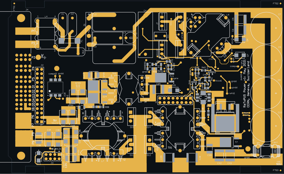
RATOPUS POWER (OHWR0048 R1) is an open-hardware circuit board from the CERN Open Hardware Repository, designed in Altium Designer: a 4-layer board of 160 × 100 mm with 268 components and 161 nets, published under CERN-OHL-W-2.0.
review 89% walked · 23 findings: 1 blocker · 14 major · 8 minor (41 items)
Open in the interactive viewerRead the full review
Design review
Probe recorded 23 findings: 1 blocker · 14 major · 8 minor (41 items) on this design. Each is shown here with its reasoning; the full review links every one to the pins, nets and datasheet pages it rests on.
- NetCopperSplitblockerOpen
Vout1's copper is in 2 pieces: IC3.2 and R41.2 are not connected to the rest of the net
Vout1's copper is in 2 pieces: IC3.2 and R41.2 are not connected to the rest of the net. Piece 1: C29.2, C30.2, C31.2, C32.2, C33.2, C34.1, C35.1, C36.1 and 13 more pin(s), on TOP_LAYER, PLANE_1, PLANE_2 and BOTTOM_LAYER, 9 drill(s), 27.57 mm2 of pour, over (4.1, 0.48) to (91.45, 33.76). Piece 2: IC3.2 and R41.2, on BOTTOM_LAYER, over (11.72, 11.4) to (17.08, 17.21). The export files every one of these pins under the net, so every connectivity check passes; the copper the fab builds leaves them apart. Usually a pour island that touches only one via of its own net, or a track ending short of its copper: join the piece to the net and export again.
At split:Vout1
Mains varistor RV1 (S14K250) is rated 250 V RMS continuous, below the upper tolerance of the 230 V RMS input
The mains varistor RV1 (S14K250) is rated 250 V RMS continuous, below the 253 V RMS top of the +/-10 % band on the board's 230 V RMS input. Run above that rating it leaks, heats, ages faster and can fail short, blowing F1.
Where it is
RV1 (B72214S0251K101 / S14K250) sits across line and neut after F1 and the common-mode choke L4, ahead of bridge D1 (sheet 3, AC/DC).
The numbers
Quantity Value Source Stated input 230 V RMS nominal ("AC Power In Nom. 230Vrms"; "230Vac From J4E") schematic sheet 3; top sheet Mains tolerance +/-10 % IEC 60038 / EN 50160 Top of the band 230 V x 1.1 = 253 V RMS derived RV1 maximum continuous operating voltage 250 V RMS (320 V DC) TDK SIOV datasheet, S14K250 row, p.9 Why it matters
A varistor run above its maximum continuous voltage leaks more, heats and ages faster, and in the limit fails short, which here would blow F1.
Fix: the next step up in the same family (S14K275, 275 V RMS) is the usual choice for 230 V lines. If the input is known to stay within 250 V RMS, record that and this can be dispositioned.
No fiducials on the bottom side, although it carries about 177 SMT parts (IC2, IC4-IC7, SOT-23s, 0805s)
There are no fiducials on the bottom side, although it carries about 177 SMT parts (IC2, IC4-IC7, SOT-23s, 0805s). A pick-and-place pass on the bottom has no board-level alignment marks.
What is on the board
The three fiducials are all top-side footprints (FIDUCIAL_TOP_C100-200): FTG1 (3.5, 98.5 mm), FTG2 (158.5, 98.5 mm), FTG3 (158.5, 1.5 mm). The bottom copper/mask render shows no fiducial at those corners or anywhere else.
Side Resistors Capacitors Diodes Transistors ICs Fiducials Source Top 12 26 3 (FTG1-FTG3) placement contract Bottom 98 47 16 9 7 (incl. IC2, IC4, IC5, IC6, IC7 in SOIC-8 and SOT-23) 0 placement contract Why it matters
The bottom carries most of the SMT assembly, so the assembler must align on pads or on panel fiducials. No part needs local fiducials (finest pitch 0.95 mm SOT-23 / 1.27 mm SOIC).
Fix: add two or three bottom-side global fiducials, or confirm that panel-rail fiducials are used.
IC7 (5 V flyback TL2843B) has no bypass capacitor on its 5 V VREF pin (refd2); the sibling controllers IC2 and IC4 each have 100 nF
IC7's 5 V reference output (pin 8, net refd2) has no local bypass capacitor, while the two sibling TL2843B controllers on this board each have 100 nF on theirs.
What is on refd2
Member Role IC7 pin 8 VREF, 5 V output R109 10k to RT/CT (rtctd2), with C82 1 nF timing cap R101 22k pull-up for the opto IC8 collector (compd2) R99 1M / D29 soft-start network (ssd2) J1 pin 12 to the RaToPUS Control Board (hand-fitted header) No capacitor is on the net on this board.
Siblings
Controller VREF net Bypass IC2 refa C18 100 nF IC4 refd1 C50 100 nF + C53 10 nF IC7 refd2 none Why it matters
The TI TL284xB application circuits show 0.1 uF on VREF. VREF supplies the pulsed charging current of the oscillator timing capacitor and the opto collector current; without local bypass, switching-frequency noise reaches RT/CT and COMP, which shows up as jitter or erratic duty cycle in the 5 V converter.
Fix
Add 100 nF X7R from refd2 to GND_D at IC7 pin 8, as on IC2 and IC4. If the Control Board places a capacitor on refd2 through J1 pin 12, that is not local to IC7 and does not replace it.
IC2 start-up bias (T4 source follower on 13 V zener D5, then D6) reaches only about 8.5 V at worst-case tolerances, below the TL2843B 9 V maximum start threshold
At worst-case tolerances, IC2's start-up supply (Vcca) reaches about 8.5 V, below the TL2843B's 9.0 V maximum start threshold, so a unit at that corner may stay in UVLO and never start. Typical margin is about 1 V.
The start-up path
IC2 is powered only by the bootstrap bias during start-up; the auxiliary winding bias (D8, T5, D10, D9) works only once IC2 is switching (sheet 3: 'Operates when Vdc>40V').
``
mermaid flowchart LR rect --> R23R26["R23 + R26 (2 x 100k)"] --> D5["D5 BZV55-B13 on T4 gate"] D5 --> T4["T4 IPA80R280P7 source follower"] --> Vcc1a --> D6["D6 PMLL4148L"] --> R32["R32 10R"] --> Vcca["Vcca = IC2 VCC"]``Vcca = Vz(D5) - Vgs(T4) - Vf(D6)
Tolerance stack
Term Typical Worst case Source Vz, D5 BZV55-B13 13.0 V 12.7 V min (at 5 mA; lower at the ~1.5 mA D5 actually runs at) BZV55 p5 Vgs(th), T4 3.0 V 3.5 V max (at 0.36 mA) IPA80R280P7 p4 Vf, D6 ~0.6 V 0.72 V max (at 5 mA) PMLL4148L p3 Vcca ~9.4 V ~8.5 V TLx843B start threshold 8.4 V 9.0 V max TL284xB p7 Suggested action
Check the margin against the real zener current and T4's transfer curve. A higher zener voltage, or taking the D6 drop out of the start-up path, restores it.
Mains bridge D1: BOM orders GBU6B (100 V) while the schematic and the BOM value say GBU6J (600 V)
The input bridge rectifier D1 of the RaToPUS 230 VAC supply is ordered as GBU6B, a 100 V part, while its BOM value and the schematic both say GBU6J (600 V). On a 230 VAC line the bridge sees about 325 V peak (more with line tolerance and surges clamped only at the 250 VAC varistor RV1); a GBU6B fitted from the MPN column would break down at first power-up.
Item Value Source D1 BOM row MPN GBU6B (FAIRCHILD), value GBU6J, 'Bridge Rectifier' BOM Schematic D1 GBU6J schematic sheet 3 GBU6B V_RRM / max RMS input 100 V / 70 V onsemi GBU6A-GBU6M data sheet p2 GBU6J V_RRM / max RMS input 600 V / 420 V same table Bridge input line / neut from J3 via F1, L4 (common-mode choke), RV1 250 VAC netlist 230 VAC peak about 325 V (about 360 V at +10 %) computed The BOM's MPN column should read GBU6J (or a higher grade). The PFC/buck stage board OHWR0049 carries the same mismatch (OBS-505).
KEMET T495 tantalums C34-C37 run at 60% of rated on the 12 V output, above KEMET's own 50% limit
C34-C37 (KEMET T495D686K020, 68 uF 20 V MnO2 tantalum) sit on the 12 V output Vout1 at 60% of their rated voltage, above the 50% maximum application voltage KEMET recommends for T495 up to 85 C; MnO2 tantalum that is under-derated can fail short and ignite.
The numbers
Quantity Value Source Rated voltage 20 V BOM T495D686K020ATE070; datasheet Operating voltage 12 V (Vout1) schematic sheet 2: 'Output: 12V, 8.33A, 100W' Applied / rated 60% arithmetic KEMET recommended max application voltage, -55 to 85 C 50% of VR KEMET T495 datasheet p.19, Recommended Voltage Derating Guidelines KEMET recommended max, 85 to 125 C 33% of VR same, p.19 Why it matters
An MnO2 tantalum on a low-impedance node (a 100 W converter output) is the case KEMET's derating exists for: the dielectric fails short and the part can burn. A 25 V or 35 V part (or a polymer type) would meet the guideline at 12 V.
Orientation
The parts are correctly oriented (+ on Vout1, other plate on GND_O); only the voltage margin is short.
BAT54C went end-of-life (Obsolete)
Vendor (DigiKey) lifecycle for BAT54C (onsemi's listing) changed from "Active" to "Obsolete" since this board was reviewed. Placed as D27, D9. A sourcing/longevity risk; consider a replacement before production.
IC5 NCP5183 high-side supply (VB-HB) sits at or below its UVLO turn-on maximum: Vccd1 is 10 V at start-up and 10.4 V running, less D23's drop
IC5 (NCP5183, 12 V active-clamp forward) has its bootstrap supply VB-HB at or below the VB UVLO turn-on maximum of 9.8 V: Vccd1 is labelled 10 V at start-up and 10.4 V running, and D23 drops a silicon diode's forward voltage before VB. A worst-case NCP5183 can hold the clamp MOSFET T7 gate off.
The supply chain across both boards
``
mermaid flowchart LR A["Vcci 10.4 V (bootstrap bias, start-up)"] -->|"D1A BAT54C"| V["Vccd1: 10V/10.4V (OHWR0047 sheet 1)"] B["Vaux1 10.8 V (auxiliary bias, running)"] -->|"D1B BAT54C"| V V -->|"J1 pin 6"| C["IC5 VCC (pin 5)"] V -->|"R81 0R, D23 ES1D"| D["IC5 VB (pin 8), C62 330 nF to HB"]``Numbers against the NCP5183 limits
Quantity Start-up Running Source Vccd1 10.0 V 10.4 V OHWR0047 R1 RATOPUS CONTROL sheet 1, label "10V/10.4V" at the D1 output VB-HB = Vccd1 - VF(D23) at 0.92 V 9.1 V 9.5 V ES1D VF 0.92 V at 1 A, ES1D p.2 VB-HB at an optimistic 0.4 V drop 9.6 V 10.0 V ES1D Fig. 2 starts at 0.4 V VB UVLO rising (min/typ/max) 7.8 / 8.8 / 9.8 V NCP5183/D p.4 VB UVLO falling (min/typ/max) 7.2 / 8.3 / 9.1 V NCP5183/D p.4 Recommended VB-HB 10 V minimum NCP5183/D p.3 VCC = Vccd1 vs VCC UVLO rising max 9.8 V +0.2 V +0.6 V NCP5183/D p.4 (VCC side holds, just) Why it matters
At start-up, VB-HB is below the 9.8 V turn-on maximum for any forward drop above 0.2 V. With the datasheet's 0.92 V it sits at the 9.1 V turn-off maximum. Even while running, it stays below the 10 V recommended minimum. A typical part (8.8 V) starts, but a part at the limit keeps DRVH low. The active clamp T7 is then never switched and reset relies on its body diode into C39. Raising Vccd1, or feeding VB through a Schottky, restores margin. The C62 droop (about 0.16 V per cycle) comes on top of this.
- concernCON-001majorOpen
[eol:BAT54C:Obsolete] BAT54C lifecycle changed from "Active" to "Obsolete" since this board was reviewed: OHWR0048 R1 RATOPUS POWER. A sourcing and longevity risk. Should this be replaced before the next build?
- PartLifecyclemajorOpen
BAT54C on 2 placements (D27, D9): the distributor catalogue reports "Obsolete" for onsemi's BAT54C
BAT54C on 2 placements (D27, D9): the distributor catalogue reports "Obsolete" for onsemi's BAT54C — a sourcing/longevity risk to confirm against the MANUFACTURER before acting. This board's BOM names FAIRCHILD SEMICONDUCTOR, and that is one line with onsemi: ON Semiconductor completed its acquisition of Fairchild Semiconductor on 2016-09-19 and renamed itself onsemi on 2021-08-05. A distributor delisting is not the same claim as the part being unavailable; check the vendor's own lifecycle/product-change notice for the status and any named successor. Re-read the source: GET /api/odb/parts/BAT54C/providers (which provider said it, the maker and part number it matched, its own words, and when we asked). THE LAST BUY DATE HAS PASSED (2018-09-30, 2,968 day(s) ago), so this is a substitution rather than a buy. The distributor reports 54,983 left. No approved alternate is recorded for this position.
At D27
- DecapViaFanoutmajorOpen
DecapViaFanout: 6 components×6
Checked by the review, stands · Claude walker W1 (Cern session) — Checked: fan-out lengths read from the copper stand; the 0.5 nH limit is Probe's starting value, not a TL2843 requirement. Left for the owner.
At C17, C50, C53, C56, C58, C79
Each finding, with its own headline
C17C17 on 'Vcca': its rail pad reaches its via over 1.38 mm of track and its ground pad over 1.91 mm, adding about 0.68 nH to its loop, past Probe's 0.5 nH starting value; put the vias at the pads
C17 on 'Vcca': its rail pad reaches its via over 1.38 mm of track and its ground pad over 1.91 mm, adding about 0.68 nH to its loop, past Probe's 0.5 nH starting value; put the vias at the pads. C17.1 (rail) runs 1.38 mm along its copper to its nearest via, 0.38 mm past the 1 mm beside the pad: 0.20 nH; C17.2 (ground) runs 1.91 mm along its copper to its nearest via, 0.91 mm past the 1 mm beside the pad: 0.48 nH. Each run past the pad as one conductor of a pair 1.80 mm apart (the pad pitch), 0.2 l ln(D/R) nH with R 0.127 mm (the track's width is not read): 0.68 nH in all. Put the vias at the pads (or in them), one per pad at least, the rail's and the ground's close together; the capacitor's own inductance as mounted is 0.84 nH (pad 0.10 nH + no via of the first net within 1 mm of its pad: the study's 0.6 nH per mm of 0.38 mm depth, ASSUMED). 0.5 nH is Probe's starting value, about the whole mounted inductance of a well-mounted 0402.
C50C50 on 'refd1': its rail pad reaches its via over 1.68 mm of track and its ground pad over 1.57 mm, adding about 0.66 nH to its loop, past Probe's 0.5 nH starting value; put the vias at the pads
C50 on 'refd1': its rail pad reaches its via over 1.68 mm of track and its ground pad over 1.57 mm, adding about 0.66 nH to its loop, past Probe's 0.5 nH starting value; put the vias at the pads. C50.2 (rail) runs 1.68 mm along its copper to its nearest via, 0.68 mm past the 1 mm beside the pad: 0.36 nH; C50.1 (ground) runs 1.57 mm along its copper to its nearest via, 0.57 mm past the 1 mm beside the pad: 0.30 nH. Each run past the pad as one conductor of a pair 1.80 mm apart (the pad pitch), 0.2 l ln(D/R) nH with R 0.127 mm (the track's width is not read): 0.66 nH in all. Put the vias at the pads (or in them), one per pad at least, the rail's and the ground's close together; the capacitor's own inductance as mounted is 0.76 nH (pad 0.10 nH + no via of the first net within 1 mm of its pad: the study's 0.6 nH per mm of 0.25 mm depth, ASSUMED). 0.5 nH is Probe's starting value, about the whole mounted inductance of a well-mounted 0402.
C53C53 on 'refd1': its rail pad reaches its via over 5.01 mm of track and its ground pad over 1.75 mm, adding about 2.52 nH to its loop, past Probe's 0.5 nH starting value; put the vias at the pads
C53 on 'refd1': its rail pad reaches its via over 5.01 mm of track and its ground pad over 1.75 mm, adding about 2.52 nH to its loop, past Probe's 0.5 nH starting value; put the vias at the pads. C53.1 (rail) runs 5.01 mm along its copper to its nearest via, 4.01 mm past the 1 mm beside the pad: 2.13 nH; C53.2 (ground) runs 1.75 mm along its copper to its nearest via, 0.75 mm past the 1 mm beside the pad: 0.40 nH. Each run past the pad as one conductor of a pair 1.80 mm apart (the pad pitch), 0.2 l ln(D/R) nH with R 0.127 mm (the track's width is not read): 2.52 nH in all. Put the vias at the pads (or in them), one per pad at least, the rail's and the ground's close together; the capacitor's own inductance as mounted is 0.76 nH (pad 0.10 nH + no via of the first net within 1 mm of its pad: the study's 0.6 nH per mm of 0.25 mm depth, ASSUMED). 0.5 nH is Probe's starting value, about the whole mounted inductance of a well-mounted 0402.
C56C56 on 'Vccd1': its rail pad reaches its via over 4.69 mm of track, adding about 1.96 nH to its loop, past Probe's 0.5 nH starting value; put the vias at the pads
C56 on 'Vccd1': its rail pad reaches its via over 4.69 mm of track, adding about 1.96 nH to its loop, past Probe's 0.5 nH starting value; put the vias at the pads. C56.2 (rail) runs 4.69 mm along its copper to its nearest via, 3.69 mm past the 1 mm beside the pad: 1.96 nH; C56.1 (ground) not measured: the pad sits in a pour of its net on its own layer, which has no track length to measure. Each run past the pad as one conductor of a pair 1.80 mm apart (the pad pitch), 0.2 l ln(D/R) nH with R 0.127 mm (the track's width is not read): 1.96 nH in all. Put the vias at the pads (or in them), one per pad at least, the rail's and the ground's close together; the capacitor's own inductance as mounted is 0.84 nH (pad 0.10 nH + no via of the first net within 1 mm of its pad: the study's 0.6 nH per mm of 0.38 mm depth, ASSUMED). 0.5 nH is Probe's starting value, about the whole mounted inductance of a well-mounted 0402.
C58C58 on 'Vccd1': its rail pad reaches its via over 1.75 mm of track and its ground pad over 1.84 mm, adding about 0.84 nH to its loop, past Probe's 0.5 nH starting value; put the vias at the pads
C58 on 'Vccd1': its rail pad reaches its via over 1.75 mm of track and its ground pad over 1.84 mm, adding about 0.84 nH to its loop, past Probe's 0.5 nH starting value; put the vias at the pads. C58.2 (rail) runs 1.75 mm along its copper to its nearest via, 0.75 mm past the 1 mm beside the pad: 0.40 nH; C58.1 (ground) runs 1.84 mm along its copper to its nearest via, 0.84 mm past the 1 mm beside the pad: 0.45 nH. Each run past the pad as one conductor of a pair 1.80 mm apart (the pad pitch), 0.2 l ln(D/R) nH with R 0.127 mm (the track's width is not read): 0.84 nH in all. Put the vias at the pads (or in them), one per pad at least, the rail's and the ground's close together; the capacitor's own inductance as mounted is 0.84 nH (pad 0.10 nH + no via of the first net within 1 mm of its pad: the study's 0.6 nH per mm of 0.38 mm depth, ASSUMED). 0.5 nH is Probe's starting value, about the whole mounted inductance of a well-mounted 0402.
C79C79 on 'Vccd2': its rail pad reaches its via over 2.19 mm of track, adding about 0.75 nH to its loop, past Probe's 0.5 nH starting value; put the vias at the pads
C79 on 'Vccd2': its rail pad reaches its via over 2.19 mm of track, adding about 0.75 nH to its loop, past Probe's 0.5 nH starting value; put the vias at the pads. C79.2 (rail) runs 2.19 mm along its copper to its nearest via, 1.19 mm past the 1 mm beside the pad: 0.75 nH; C79.1 (ground) not measured: its own track joins it to IC7.5 (2.48 mm) before any via: it serves that pin directly, and its loop does not run through its vias. Each run past the pad as one conductor of a pair 3.00 mm apart (the pad pitch), 0.2 l ln(D/R) nH with R 0.127 mm (the track's width is not read): 0.75 nH in all. Put the vias at the pads (or in them), one per pad at least, the rail's and the ground's close together; the capacitor's own inductance as mounted is 1.23 nH (pad 0.20 nH + no via of the first net within 1 mm of its pad: the study's 0.6 nH per mm of 0.38 mm depth, ASSUMED). 0.5 nH is Probe's starting value, about the whole mounted inductance of a well-mounted 0402.
- PartLifecyclemajorOpen
PartLifecycle: 3 part numbers×3
3 Obsolete · on 7 placements
At C1, C32, L1
Each finding, with its own headline
C1DE2F3KY103MA3BM02F on 2 placements (C1, C2): the distributor catalogue reports "Obsolete" for Murata Electronics's DE2F3KY103MA3BM02F
DE2F3KY103MA3BM02F on 2 placements (C1, C2): the distributor catalogue reports "Obsolete" for Murata Electronics's DE2F3KY103MA3BM02F — a sourcing/longevity risk to confirm against the MANUFACTURER before acting. That is the maker this board's BOM names (MURATA). A distributor delisting is not the same claim as the part being unavailable; check the vendor's own lifecycle/product-change notice for the status and any named successor. Re-read the source: GET /api/odb/parts/DE2F3KY103MA3BM02F/providers (which provider said it, the maker and part number it matched, its own words, and when we asked). THE LAST BUY DATE HAS PASSED (2024-03-31, 959 day(s) ago), so this is a substitution rather than a buy. The distributor reports NONE left. No approved alternate is recorded for this position.
C32CKG45NX7S2A106M500JH on 4 placements (C32, C33, C38, C69): the distributor catalogue reports "Obsolete" for TDK's CKG45NX7S2A106M500JH
CKG45NX7S2A106M500JH on 4 placements (C32, C33, C38, C69): the distributor catalogue reports "Obsolete" for TDK's CKG45NX7S2A106M500JH — a sourcing/longevity risk to confirm against the MANUFACTURER before acting. That is the maker this board's BOM names (TDK). A distributor delisting is not the same claim as the part being unavailable; check the vendor's own lifecycle/product-change notice for the status and any named successor. Re-read the source: GET /api/odb/parts/CKG45NX7S2A106M500JH/providers (which provider said it, the maker and part number it matched, its own words, and when we asked). No approved alternate is recorded for this position.
L1B82144B2473J000 on L1: the distributor catalogue reports "Obsolete" for TDK's B82144B2473J000
B82144B2473J000 on L1: the distributor catalogue reports "Obsolete" for TDK's B82144B2473J000 — a sourcing/longevity risk to confirm against the MANUFACTURER before acting. That is the maker this board's BOM names (TDK). A distributor delisting is not the same claim as the part being unavailable; check the vendor's own lifecycle/product-change notice for the status and any named successor. Re-read the source: GET /api/odb/parts/B82144B2473J000/providers (which provider said it, the maker and part number it matched, its own words, and when we asked). THE LAST BUY DATE HAS PASSED (2026-08-31, 76 day(s) ago), so this is a substitution rather than a buy. The distributor reports 384 left. No approved alternate is recorded for this position.
- ReferencePlaneDiscontinuitymajorOpen
ReferencePlaneDiscontinuity: 8 boards×8
Checked by the review, stands · Claude walker W1 (Cern session) — Checked: splits, voids and reference changes read from the copper stand; they sit on slow PWM, timing and sense nets of ~100 kHz converters, and no datasheet or app note on file sets a limit. Left for the owner.
At along@PLANE_2:GND_C|GND_D, split@PLANE_2:GND_C|GND_D, split@PLANE_2:GND_D|rect, void:GND_C@PLANE_2:106.76,73.96, void:GND_D@PLANE_2:52.22,61.65, void:GND_D@PLANE_2:96.61,65.13, void:routed@BOTTOM_LAYER|PLANE_2, void:routed@PLANE_1|TOP_LAYER
Each finding, with its own headline
along@PLANE_2:GND_C|GND_D'rtcta' runs ALONG the split between the GND_C and GND_D planes on PLANE_2 at 1 place, the longest 5.08 mm; the impedance rises from 43 ohm to 52 ohm there at worst, 9.1 % of each edge reflected (fastest: rtcta at 100 ps 10-90 %, ASSUMED)
On PLANE_2 the GND_C and GND_D planes part, and 'rtcta' runs down the slot between them at 1 place(s), rather than across it. This is not a crossing: the return still follows the track, in the plane on its other side and in the slot's edges, so it does not detour. What changes is the track's own impedance. With the plane gone from under it on this side for that length, its field reaches further, to the slot's edges and to the next plane beyond, so its capacitance falls and its impedance rises; every edge travelling down it is partly reflected where it enters the stretch and again where it leaves, by (Z2 - Z1)/(Z2 + Z1). The longer the stretch against the edge's rise, the more of the edge sees the full step. A crossing is generally the worse fault; a mismatch is not free. Over solid plane each track is 43 ohm; along the slot 52 ohm, reflecting up to 9.1 % of each edge (a method-of-moments field solve of the cross-section, one dielectric; were the slot's edges to carry none of the return, up to 54 ohm). No place stays within 10 %, the tolerance controlled impedance is commonly built to (the stackup states none), so the finding is a warning. One decision covers the split line's slot: whether these tracks may run down it, or should be moved over solid plane.
- 'rtcta' on BOTTOM_LAYER at (118.73, 58.55), 6.41 mm, running ALONG the split for 5.08 mm, not across it, 43 ohm over solid plane, 52 ohm along it: 9.1 % of each edge reflected; other side: none: the signal layer is outermost
Every site is a row of this finding's evidence, keyed by net, layers and position. GET /api/odb/boards/49/reference-planes?group=along%40PLANE_2%3AGND_C%7CGND_D serves each with its own layer_image region; all of them lie in x 115.36..121.53, y 55.76..62.48 mm (board frame, Y up).
Read from the copper as drawn on the reference layer, along each track's centreline at exact breakpoints. The reference is the copper beside the track, never the layer's type or name. Whether it matters depends on each signal's edge rate, which nothing on file states for these nets: a slow static line crosses a split harmlessly, a fast edge does not.
split@PLANE_2:GND_C|GND_D4 nets cross the split between the GND_C and GND_D planes on PLANE_2 at 4 places, with no plane on the track's other side (fastest: csd2 at 100 ps 10-90 %, ASSUMED)
On PLANE_2 the GND_C and GND_D planes part, and 4 nets cross from one to the other at 4 place(s). The return current cannot follow a track across; it detours to wherever the two planes are joined (a stitching capacitor, or the source), and the loop it opens radiates and couples. One decision covers the boundary: whether it is stitched near these crossings, or the nets crossing it are slow enough not to care. Tracks that run ALONG this split, down the slot rather than across it, are a finding of their own: theirs is an impedance step, not a detour. At 0 of the 4 crossing(s) the track's other neighbour carries a plane, which the return can use there; 4 are on an outer layer, with no other neighbour. No crossing has a plane on the track's other side, so the whole return meets the break.
- 'csd2' on BOTTOM_LAYER at (95.5, 66.38), 1.85 mm; other side: none: the signal layer is outermost
- 'ipk2' on BOTTOM_LAYER at (105.45, 57.29), 4.05 mm; other side: none: the signal layer is outermost
- 'isns' on BOTTOM_LAYER at (109.02, 74.6), 5 mm; other side: none: the signal layer is outermost
- 'rtcta' on BOTTOM_LAYER at (114.4, 55.78), 1.1 mm; other side: none: the signal layer is outermost
Every site is a row of this finding's evidence, keyed by net, layers and position. GET /api/odb/boards/49/reference-planes?group=split%40PLANE_2%3AGND_C%7CGND_D serves each with its own layer_image region; all of them lie in x 94.4..115.4, y 54.23..78.62 mm (board frame, Y up).
Read from the copper as drawn on the reference layer, along each track's centreline at exact breakpoints. The reference is the copper beside the track, never the layer's type or name. Whether it matters depends on each signal's edge rate, which nothing on file states for these nets: a slow static line crosses a split harmlessly, a fast edge does not.
split@PLANE_2:GND_D|rect'hin' crosses the split between the GND_D and rect planes on PLANE_2 at 1 place, with no plane on the track's other side (fastest: hin at 100 ps 10-90 %, ASSUMED)
On PLANE_2 the GND_D and rect planes part, and 'hin' crosses from one to the other at 1 place(s). The return current cannot follow a track across; it detours to wherever the two planes are joined (a stitching capacitor, or the source), and the loop it opens radiates and couples. One decision covers the boundary: whether it is stitched near these crossings, or the nets crossing it are slow enough not to care. Tracks that run ALONG this split, down the slot rather than across it, are a finding of their own: theirs is an impedance step, not a detour. At 0 of the 1 crossing(s) the track's other neighbour carries a plane, which the return can use there; 1 are on an outer layer, with no other neighbour. No crossing has a plane on the track's other side, so the whole return meets the break.
- 'hin' on BOTTOM_LAYER at (141.75, 39.96), 7.89 mm; other side: none: the signal layer is outermost
Every site is a row of this finding's evidence, keyed by net, layers and position. GET /api/odb/boards/49/reference-planes?group=split%40PLANE_2%3AGND_D%7Crect serves each with its own layer_image region; all of them lie in x 140.55..142.75, y 35.1..44.83 mm (board frame, Y up).
Read from the copper as drawn on the reference layer, along each track's centreline at exact breakpoints. The reference is the copper beside the track, never the layer's type or name. Whether it matters depends on each signal's edge rate, which nothing on file states for these nets: a slow static line crosses a split harmlessly, a fast edge does not.
void:GND_C@PLANE_2:106.76,73.96'pwma' crosses where the outline of the GND_C plane on PLANE_2 is drawn back, at 1 place, the longest 11.51 mm (fastest: pwma at 100 ps 10-90 %, ASSUMED)
Along 'pwma' on BOTTOM_LAYER, the GND_C plane on PLANE_2 has 11.51 mm under the track with no copper, at (106.76, 73.96), the same plane on both sides. No single drill's anti-pad and no landing explains it: a clearance is excused only when it holds a drill and is drawn round it, or the track ends in it on the net's own pad or via, or runs through its own via's clearance and no farther. The return current detours round the void. 1 of them run ALONG the bare copper, parallel to its edges, rather than across it (the longest 6.05 mm). No hole cleared it: the outline of the pour at x 97.63..132.1, y 56.33..89.3 is drawn back there. One decision covers the void: whether these tracks may cross it, or the plane should be filled under them. No crossing has a plane on the track's other side, so the whole return meets the break.
- 'pwma' on BOTTOM_LAYER at (106.76, 73.96), 11.51 mm, running ALONG the bare copper for 6.05 mm, not across it over no copper; other side: none: the signal layer is outermost
Every site is a row of this finding's evidence, keyed by net, layers and position. GET /api/odb/boards/49/reference-planes?group=void%3AGND_C%40PLANE_2%3A106.76%2C73.96 serves each with its own layer_image region; all of them lie in x 102.55..110.98, y 67.7..78.55 mm (board frame, Y up).
Read from the copper as drawn on the reference layer, along each track's centreline at exact breakpoints. The reference is the copper beside the track, never the layer's type or name. Whether it matters depends on each signal's edge rate, which nothing on file states for these nets: a slow static line crosses a split harmlessly, a fast edge does not.
void:GND_D@PLANE_2:52.22,61.65'compd2' crosses where the outline of the GND_D plane on PLANE_2 is drawn back, at 1 place, the longest 47.72 mm (fastest: compd2 at 100 ps 10-90 %, ASSUMED)
Along 'compd2' on BOTTOM_LAYER, the GND_D plane on PLANE_2 has 47.72 mm under the track with copper of GND_D, not a plane, at (52.22, 61.65), running to the end of the track. No single drill's anti-pad and no landing explains it: a clearance is excused only when it holds a drill and is drawn round it, or the track ends in it on the net's own pad or via, or runs through its own via's clearance and no farther. The return current detours round the void. 1 of them run ALONG the bare copper, parallel to its edges, rather than across it (the longest 41.21 mm). No hole cleared it: the outline of the pour at x 72.98..74.95, y 60.08..61.5 is drawn back there. One decision covers the void: whether these tracks may cross it, or the plane should be filled under them. No crossing has a plane on the track's other side, so the whole return meets the break.
- 'compd2' on BOTTOM_LAYER at (52.22, 61.65), 47.72 mm, running ALONG the bare copper for 41.21 mm, not across it over copper of GND_D, not a plane, to the end of the track; other side: none: the signal layer is outermost
Every site is a row of this finding's evidence, keyed by net, layers and position. GET /api/odb/boards/49/reference-planes?group=void%3AGND_D%40PLANE_2%3A52.22%2C61.65 serves each with its own layer_image region; all of them lie in x 26.38..73.98, y 55.35..62.65 mm (board frame, Y up).
Read from the copper as drawn on the reference layer, along each track's centreline at exact breakpoints. The reference is the copper beside the track, never the layer's type or name. Whether it matters depends on each signal's edge rate, which nothing on file states for these nets: a slow static line crosses a split harmlessly, a fast edge does not.
void:GND_D@PLANE_2:96.61,65.13'csd2' crosses where the outline of the GND_D plane on PLANE_2 is drawn back, at 1 place, the longest 1.93 mm (fastest: csd2 at 100 ps 10-90 %, ASSUMED)
Along 'csd2' on BOTTOM_LAYER, the GND_D plane on PLANE_2 has 1.93 mm under the track with no copper, at (96.61, 65.13), the same plane on both sides. No single drill's anti-pad and no landing explains it: a clearance is excused only when it holds a drill and is drawn round it, or the track ends in it on the net's own pad or via, or runs through its own via's clearance and no farther. The return current detours round the void. 1 of them run ALONG the bare copper, parallel to its edges, rather than across it (the longest 0.94 mm). No hole cleared it: the outline of the pour at x 51.45..148.63, y 6.13..67.73 is drawn back there. One decision covers the void: whether these tracks may cross it, or the plane should be filled under them. No crossing has a plane on the track's other side, so the whole return meets the break.
- 'csd2' on BOTTOM_LAYER at (96.61, 65.13), 1.93 mm, running ALONG the bare copper for 0.94 mm, not across it over no copper; other side: none: the signal layer is outermost
Every site is a row of this finding's evidence, keyed by net, layers and position. GET /api/odb/boards/49/reference-planes?group=void%3AGND_D%40PLANE_2%3A96.61%2C65.13 serves each with its own layer_image region; all of them lie in x 94.9..98.68, y 63.78..66.13 mm (board frame, Y up).
Read from the copper as drawn on the reference layer, along each track's centreline at exact breakpoints. The reference is the copper beside the track, never the layer's type or name. Whether it matters depends on each signal's edge rate, which nothing on file states for these nets: a slow static line crosses a split harmlessly, a fast edge does not.
void:routed@BOTTOM_LAYER|PLANE_2'pwma' on BOTTOM_LAYER crosses the tracks routed through the GND_C pour on PLANE_2 at 1 place, the longest 1.46 mm (fastest: pwma at 100 ps 10-90 %, ASSUMED)
The GND_C pour on PLANE_2 is cleared round tracks routed through it, and tracks on BOTTOM_LAYER, which take that pour as their reference, cross them: for the width of each cut the return has no plane under it and detours round the cut. 1 place(s) on 1 net(s). One decision covers the layer pair: whether these layers may take a pour their own tracks cut as the reference, or the routing or the stackup should give the tracks a plane that is not cut where they cross. No crossing has a plane on the track's other side, so the whole return meets the break.
- 'pwma' on BOTTOM_LAYER at (103.55, 78.9), 1.46 mm over copper of isns, not a plane; other side: none: the signal layer is outermost
Every site is a row of this finding's evidence, keyed by net, layers and position. GET /api/odb/boards/49/reference-planes?group=void%3Arouted%40BOTTOM_LAYER%7CPLANE_2 serves each with its own layer_image region; all of them lie in x 102.55..104.55, y 77.17..80.63 mm (board frame, Y up).
Read from the copper as drawn on the reference layer, along each track's centreline at exact breakpoints. The reference is the copper beside the track, never the layer's type or name. Whether it matters depends on each signal's edge rate, which nothing on file states for these nets: a slow static line crosses a split harmlessly, a fast edge does not.
void:routed@PLANE_1|TOP_LAYER'ipk1' on TOP_LAYER crosses the tracks routed through the Vcca pour on PLANE_1 at 1 place, the longest 21.43 mm; 1 runs ALONG the cut round another net's track (fastest: ipk1 at 100 ps 10-90 %, ASSUMED)
The Vcca pour on PLANE_1 is cleared round tracks routed through it, and tracks on TOP_LAYER, which take that pour as their reference, cross them: for the width of each cut the return has no plane under it and detours round the cut. 1 place(s) on 1 net(s). 1 of the crossings run ALONG the cut round another net's track rather than across it, parallel to its edges (the longest 12.85 mm): over or right beside that track, broadside to it as well as off the plane. One decision covers the layer pair: whether these layers may take a pour their own tracks cut as the reference, or the routing or the stackup should give the tracks a plane that is not cut where they cross. No crossing has a plane on the track's other side, so the whole return meets the break.
- 'ipk1' on TOP_LAYER at (105.9, 53.89), 21.43 mm, running ALONG the bare copper for 12.85 mm, not across it over copper of Vdc, not a plane, to the end of the track; other side: none: the signal layer is outermost
Every site is a row of this finding's evidence, keyed by net, layers and position. GET /api/odb/boards/49/reference-planes?group=void%3Arouted%40PLANE_1%7CTOP_LAYER serves each with its own layer_image region; all of them lie in x 99.99..108.9, y 42.46..62.45 mm (board frame, Y up).
Read from the copper as drawn on the reference layer, along each track's centreline at exact breakpoints. The reference is the copper beside the track, never the layer's type or name. Whether it matters depends on each signal's edge rate, which nothing on file states for these nets: a slow static line crosses a split harmlessly, a fast edge does not.
- FiducialMissingmajorOpen
The bottom side carries 177 SMT component(s) and no fiducial was found on it
The bottom side carries 177 SMT component(s) but no fiducial was found on it — a placement machine has no optical reference to align to. Probe found no pad labelled .pad_usage=g_fiducial/l_fiducial (basis pad_usage); no single-pad, netless, undrilled component whose 0.5-3 mm round pad has a concentric solder-mask opening at least 1.5x its diameter with no other copper inside it (basis geometry); and no component whose refdes starts FID or whose part or package name contains FIDUCIAL (basis footprint-name). The other side has 3, found by geometry (1), footprint-name (2). If your library names fiducials something Probe does not recognise, mark this benign — disposition_finding(rule='FiducialMissing', entity='bottom', status='benign', reason=…) — the name match only ever silences this check, it never asserts anything. If the side really has no fiducial, say so with status='confirmed': that answers the finding and keeps it gating release.
At bottom
12 V output TVS D13 (SMBJ12A) has a 12 V working standoff: equal to the nominal Vout1, so no margin above it
The 12 V output TVS D13 (SMBJ12A) has a 12 V working standoff, equal to the nominal Vout1, so any positive tolerance, ripple or overshoot puts it above its rated standoff. If Vout1 never exceeds 12.0 V, this can be dispositioned.
The numbers
D13 (onsemi SMBJ12A) clamps Vout1 to GND_O next to J4.
Quantity Value Source Vout1 nominal 12 V, 100 W ("Vout1 12 V, 100W") schematic sheet 2 D13 working peak reverse voltage 12 V SMBJ12A datasheet, p.1 Leakage 5 uA max, specified only up to 12 V SMBJ12A datasheet, p.2 Breakdown at 1 mA 13.2 V min / 14.3 V max SMBJ12A datasheet, p.2 IC3/LD1 indicator threshold lights above about 11.3 V board indicator circuit Why it matters
The output's nominal voltage is exactly the TVS standoff. Any positive regulation tolerance, ripple or load-release overshoot puts D13 above its rated standoff, where leakage is not specified and, toward 13.2 V, the part starts to conduct and dissipate.
The IC3/LD1 indicator shows the output is expected above 11.3 V, but not how far above 12 V it may go.
Fix: a part whose standoff is above the output's maximum would keep the clamp out of normal operation. If Vout1 is regulated so it never exceeds 12.0 V, this can be dispositioned.
Three schematic design notes lost their key words to spreadsheet '#NAME?' errors (R79 slope note, Vdc and PFC cold-point notes)
Three schematic design notes lost their key words to spreadsheet "#NAME?" errors: the R79 slope note and the Vdc cold-point note on sheet 2, and the PFC cold-point note on sheet 3.
"#NAME?" is the error a spreadsheet shows when a cell starting with "=" (for example an arrow "=>") is evaluated. The damaged notes:
- Sheet 2 (12V DC/DC): "NOTE: Lower R79 #NAME? Greater slope compensation". The relation between R79 and the slope is lost. The slope-compensation network drawn beside it is R84/R87, with no R79 on this sheet.
- Sheet 2 (12V DC/DC): "Vdc node is a cold point from EMI perspective and a heat sink for transformer primary winding #NAME? Use as large area of copper as possible".
- Sheet 3 (AC/DC): "... heat sink for the PFC inductor winding #NAME? Use as large Cu area as possible".
These notes carry layout and tuning intent that a reviewer or re-spinner needs.
Fix: retype them without the leading "=".
Five bottom-side reference designators are mirrored and read backwards: D8, D21, IC3, C30, C58
Five bottom-side reference designators are mirrored and read backwards on the real board: D8, D21, IC3, C30 and C58.
In a bottom-view render of BOTTOM_OVERLAY, where correctly placed bottom text reads normally, these five are drawn mirrored while every neighbour (R44, R47, R73, R85, C59, C31, C25) reads correctly.
- Affected: D8, D21, IC3, C30, C58
- C58 sits beside a correctly drawn C59; IC3 is the LM4041 that drives LD1.
This slows rework and inspection and invites misidentification. Text size is otherwise at the printable floor: bottom designators measure about 0.8-0.85 mm cap height with about 0.1 mm stroke.
Fix: re-mirror the five labels.
Schematic title blocks say 'Sheet 1 of 1' on all four sheets of the published set, although the design has four sheets numbered 1-4
Every sheet of the RaToPUS Power v1 schematic set says "Sheet 1 of 1" in its title block, although the set has four sheets (Number 1-4), so a printed or single-page copy cannot tell a reader that sheets are missing.
What the title blocks say
Sheet (file) Number field Sheet field Source Top (1-top.schdoc) 1 1 of 1 designer PDF p.4; Probe schematic p.4 AC/DC (2-ac-dc.schdoc) 2 1 of 1 designer PDF p.3; Probe schematic p.3 12V DC/DC (3-dc-dc-12v.schdoc) 3 1 of 1 designer PDF p.2; Probe schematic p.2 5V DC/DC (4-dc-dc-5v.schdoc) 4 1 of 1 designer PDF p.1; Probe schematic p.1 The designer's published PDF (
ratopus/RaToPUS-Power-v1-May-2021/RaToPUS-Power-v1-May-2021.pdfin the OHWR repository psu-rad-acdc-230v-12v5v-110w, commit aa0f8b8) reads, for example, "Number: 4 Revision: 1 ... Date: 04/06/2021 Time: 15:38:44 Sheet 1 of 1". Each sheet is still identifiable by its title, Number field, revision, designer and CERN address.What this finding no longer claims
The earlier wording (OBS-85) also said the date field showed a print date instead of a release date, and that the logos rendered as "Cannot open file C:\DIOT_RTPS\..." errors. Neither is in the designer's document:
- The schematic PDF on the Probe box was re-exported from the Altium sources by the CERN conversion on 2026-09-22. Its File field shows the conversion machine's path (
C:\tmp\claude\cern\ohwr\repos\...). The logo errors appear because the logo images sit at the designer's local path, which does not exist on that machine. - The designer's own PDF has no such error text (none of its pages contains "Cannot open") and a date of 04/06/2021, consistent with the May 2021 release.
Fix: set the sheet-count parameters (sheet number and sheet total) so that each sheet reads n of 4.
- The schematic PDF on the Probe box was re-exported from the Altium sources by the CERN conversion on 2026-09-22. Its File field shows the conversion machine's path (
- ReferencePlaneDiscontinuityminorOpen
3 nets change reference between GND_D and Vccd1 at 5 vias, none with a reference that continues across (fastest: csd1 at 100 ps 10-90 %, ASSUMED)
At 5 via(s), on 3 net(s), the signal leaves a layer referenced by one of GND_D and Vccd1 for a layer referenced by the other, and no plane references both layers. Different nets: no via can carry the return across; only decoupling between the two planes near the via can. The capacitor carrying the return across was measured at each via, at the knee of the crossing net's edge against 50 ohm assumed: 5 served. Every site is served, so the finding is the lower tier (info). 5 of them at an ASSUMED edge (no edge on file for the net): state one (net_timing_state) and it is re-read. One decision covers the pair: whether GND_D and Vccd1 are decoupled to each other near these vias. A via whose layers have more references than these two is a site of each pair it joins. None is partial: at every one, no reference continues across the via.
- 'lin' at (136.87, 33.63), TOP_LAYER -> BOTTOM_LAYER: Vccd1 on PLANE_1 to GND_D on PLANE_2; pure, no reference continues across; stitching served, 25.5 mm of track past the via on BOTTOM_LAYER: At the 5 GHz knee of a 100 ps edge (100 ps 10-90 %, assumed: no edge is on file for the net) no capacitor carries the return; only the planes do. GND_D on PLANE_2 and Vccd1 on PLANE_1 are adjacent, 0.127 mm apart: their own capacitance carries the return. Served.
- 'lin' at (140.33, 33.35), TOP_LAYER -> BOTTOM_LAYER: Vccd1 on PLANE_1 to GND_D on PLANE_2; pure, no reference continues across; stitching served, 25.5 mm of track past the via on BOTTOM_LAYER: At the 5 GHz knee of a 100 ps edge (100 ps 10-90 %, assumed: no edge is on file for the net) no capacitor carries the return; only the planes do. GND_D on PLANE_2 and Vccd1 on PLANE_1 are adjacent, 0.127 mm apart: their own capacitance carries the return. Served.
- 'hin' at (136.46, 34.9), TOP_LAYER -> BOTTOM_LAYER: Vccd1 on PLANE_1 to GND_D on PLANE_2; pure, no reference continues across; stitching served, 25.2 mm of track past the via on BOTTOM_LAYER: At the 5 GHz knee of a 100 ps edge (100 ps 10-90 %, assumed: no edge is on file for the net) no capacitor carries the return; only the planes do. GND_D on PLANE_2 and Vccd1 on PLANE_1 are adjacent, 0.127 mm apart: their own capacitance carries the return. Served.
- 'hin' at (140.35, 34.9), TOP_LAYER -> BOTTOM_LAYER: Vccd1 on PLANE_1 to GND_D on PLANE_2; pure, no reference continues across; stitching served, 25.2 mm of track past the via on BOTTOM_LAYER: At the 5 GHz knee of a 100 ps edge (100 ps 10-90 %, assumed: no edge is on file for the net) no capacitor carries the return; only the planes do. GND_D on PLANE_2 and Vccd1 on PLANE_1 are adjacent, 0.127 mm apart: their own capacitance carries the return. Served.
- 'csd1' at (111.32, 48.97), TOP_LAYER -> BOTTOM_LAYER: Vccd1 on PLANE_1 to GND_D on PLANE_2; pure, no reference continues across; stitching served, 21.5 mm of track past the via on BOTTOM_LAYER: At the 5 GHz knee of a 100 ps edge (100 ps 10-90 %, assumed: no edge is on file for the net) no capacitor carries the return; only the planes do. GND_D on PLANE_2 and Vccd1 on PLANE_1 are adjacent, 0.127 mm apart: their own capacitance carries the return. Served.
Every site is a row of this finding's evidence, keyed by net, layers and position. GET /api/odb/boards/49/reference-planes?group=refchange%3AGND_D%7CVccd1 serves each with its own layer_image region; all of them lie in x 109.32..142.35, y 31.35..50.97 mm (board frame, Y up).
The reference on each layer is the first plane the track meets leaving the via, anti-pads and the net's own copper skipped. Whether it matters depends on each signal's edge rate, which nothing on file states for these nets: a slow static line crosses a split harmlessly, a fast edge does not.
At refchange:GND_D|Vccd1
- DecapViaFanoutminorOpen
C59 on 'Vccd1': its rail pad reaches its via over 4.25 mm of track and its ground pad over 4.67 mm, adding about 4.28 nH to its loop, past Probe's 0.5 nH starting value; put the vias at the pads (a 10 uF bulk capacitor: its inductance matters only far above the band it serves)
C59 on 'Vccd1': its rail pad reaches its via over 4.25 mm of track and its ground pad over 4.67 mm, adding about 4.28 nH to its loop, past Probe's 0.5 nH starting value; put the vias at the pads (a 10 uF bulk capacitor: its inductance matters only far above the band it serves). C59.2 (rail) runs 4.25 mm along its copper to its nearest via, 3.25 mm past the 1 mm beside the pad: 2.01 nH; C59.1 (ground) runs 4.67 mm along its copper to its nearest via, 3.67 mm past the 1 mm beside the pad: 2.27 nH. Each run past the pad as one conductor of a pair 2.80 mm apart (the pad pitch), 0.2 l ln(D/R) nH with R 0.127 mm (the track's width is not read): 4.28 nH in all. Put the vias at the pads (or in them), one per pad at least, the rail's and the ground's close together; the capacitor's own inductance as mounted is 1.23 nH (pad 0.20 nH + no via of the first net within 1 mm of its pad: the study's 0.6 nH per mm of 0.38 mm depth, ASSUMED). 0.5 nH is Probe's starting value, about the whole mounted inductance of a well-mounted 0402.
At C59
- ConnectorDomainMixedminorOpen
ConnectorDomainMixed: 4 components×4
4 checked by the review by Claude walker W1 (Cern session) — 4 different reasons
At J1, J2, J3, J4
Each finding, with its own headline
J1J1 takes 5 different supplies off the board on one connector: Vdc (50.0 V), 13p7v (13.7 V), Vcci (10.4 V), refd1 (5.0 V), refd2 (5.0 V)
J1 carries 5 different supplies out of the board on one connector: Vdc (50.0 V) on 1, 13p7v (13.7 V) on 10, Vcci (10.4 V) on 14, refd1 (5.0 V) on 7, refd2 (5.0 V) on 12. Declare the intent. Two rails on one connector is ordinary in a docking or power-distribution interface and a hazard in a signal one, and the difference is not visible from the netlist — but note that adjacent contacts at different voltages are exactly what a mirrored, reversed or off-by-one cable shorts together, so the cost of getting the mating wrong is a rail collision rather than a dead signal. If this is a standard connector, declare its family (connector_family_declare) and file the standard's contact map: supplies on the contacts it assigns to power are then not reported.
J2J2 takes 2 different supplies off the board on one connector: Vout1 (12.0 V), Vout2 (5.0 V)
J2 carries 2 different supplies out of the board on one connector: Vout1 (12.0 V) on 1, Vout2 (5.0 V) on 3. Declare the intent. Two rails on one connector is ordinary in a docking or power-distribution interface and a hazard in a signal one, and the difference is not visible from the netlist — but note that adjacent contacts at different voltages are exactly what a mirrored, reversed or off-by-one cable shorts together, so the cost of getting the mating wrong is a rail collision rather than a dead signal. If this is a standard connector, declare its family (connector_family_declare) and file the standard's contact map: supplies on the contacts it assigns to power are then not reported.
J3J3 takes 2 different supplies off the board on one connector: Vout1 (12.0 V), Vout2 (5.0 V)
J3 carries 2 different supplies out of the board on one connector: Vout1 (12.0 V) on 1, Vout2 (5.0 V) on 7. Declare the intent. Two rails on one connector is ordinary in a docking or power-distribution interface and a hazard in a signal one, and the difference is not visible from the netlist — but note that adjacent contacts at different voltages are exactly what a mirrored, reversed or off-by-one cable shorts together, so the cost of getting the mating wrong is a rail collision rather than a dead signal. If this is a standard connector, declare its family (connector_family_declare) and file the standard's contact map: supplies on the contacts it assigns to power are then not reported.
J4J4 takes 2 different supplies off the board on one connector: Vout1 (12.0 V), Vout2 (5.0 V)
J4 carries 2 different supplies out of the board on one connector: Vout1 (12.0 V) on P8/P9, Vout2 (5.0 V) on C5/C6/D6. Declare the intent. Two rails on one connector is ordinary in a docking or power-distribution interface and a hazard in a signal one, and the difference is not visible from the netlist — but note that adjacent contacts at different voltages are exactly what a mirrored, reversed or off-by-one cable shorts together, so the cost of getting the mating wrong is a rail collision rather than a dead signal. If this is a standard connector, declare its family (connector_family_declare) and file the standard's contact map: supplies on the contacts it assigns to power are then not reported.
- ReferencePlaneDiscontinuityminorOpen
ReferencePlaneDiscontinuity: 2 boards×2
Checked by the review, stands · Claude walker W1 (Cern session) — Checked: splits, voids and reference changes read from the copper stand; they sit on slow PWM, timing and sense nets of ~100 kHz converters, and no datasheet or app note on file sets a limit. Left for the owner.
At refchange:GND_C|Vcca, refchange:GND_D|Vccd2
Each finding, with its own headline
refchange:GND_C|Vcca'pwma' changes reference between GND_C and Vcca at 2 vias, none with a reference that continues across (fastest: pwma at 100 ps 10-90 %, ASSUMED)
At 2 via(s), on 1 net(s), the signal leaves a layer referenced by one of GND_C and Vcca for a layer referenced by the other, and no plane references both layers. Different nets: no via can carry the return across; only decoupling between the two planes near the via can. The capacitor carrying the return across was measured at each via, at the knee of the crossing net's edge against 50 ohm assumed: 2 served. Every site is served, so the finding is the lower tier (info). 2 of them at an ASSUMED edge (no edge on file for the net): state one (net_timing_state) and it is re-read. One decision covers the pair: whether GND_C and Vcca are decoupled to each other near these vias. A via whose layers have more references than these two is a site of each pair it joins. None is partial: at every one, no reference continues across the via.
- 'pwma' at (109.97, 62.68), TOP_LAYER -> BOTTOM_LAYER: Vcca on PLANE_1 to GND_C on PLANE_2; pure, no reference continues across; stitching served, 35.5 mm of track past the via on BOTTOM_LAYER: At the 5 GHz knee of a 100 ps edge (100 ps 10-90 %, assumed: no edge is on file for the net) no capacitor carries the return; only the planes do. GND_C on PLANE_2 and Vcca on PLANE_1 are adjacent, 0.127 mm apart: their own capacitance carries the return. Served.
- 'pwma' at (109.97, 66.75), TOP_LAYER -> BOTTOM_LAYER: Vcca on PLANE_1 to GND_C on PLANE_2; pure, no reference continues across; stitching served, 35.5 mm of track past the via on BOTTOM_LAYER: At the 5 GHz knee of a 100 ps edge (100 ps 10-90 %, assumed: no edge is on file for the net) no capacitor carries the return; only the planes do. GND_C on PLANE_2 and Vcca on PLANE_1 are adjacent, 0.127 mm apart: their own capacitance carries the return. Served.
Every site is a row of this finding's evidence, keyed by net, layers and position. GET /api/odb/boards/49/reference-planes?group=refchange%3AGND_C%7CVcca serves each with its own layer_image region; all of them lie in x 107.97..111.97, y 60.68..68.75 mm (board frame, Y up).
The reference on each layer is the first plane the track meets leaving the via, anti-pads and the net's own copper skipped. Whether it matters depends on each signal's edge rate, which nothing on file states for these nets: a slow static line crosses a split harmlessly, a fast edge does not.
refchange:GND_D|Vccd2'csd2_uf' changes reference between GND_D and Vccd2 at a via, none with a reference that continues across (fastest: csd2_uf at 100 ps 10-90 %, ASSUMED)
At 1 via(s), on 1 net(s), the signal leaves a layer referenced by one of GND_D and Vccd2 for a layer referenced by the other, and no plane references both layers. Different nets: no via can carry the return across; only decoupling between the two planes near the via can. The capacitor carrying the return across was measured at each via, at the knee of the crossing net's edge against 50 ohm assumed: 1 served. Every site is served, so the finding is the lower tier (info). 1 of them at an ASSUMED edge (no edge on file for the net): state one (net_timing_state) and it is re-read. One decision covers the pair: whether GND_D and Vccd2 are decoupled to each other near these vias. A via whose layers have more references than these two is a site of each pair it joins. None is partial: at every one, no reference continues across the via.
- 'csd2_uf' at (90.92, 63.7), TOP_LAYER -> BOTTOM_LAYER: Vccd2 on PLANE_1 to GND_D on PLANE_2; pure, no reference continues across; stitching served, 3.2 mm of track past the via on BOTTOM_LAYER: At the 5 GHz knee of a 100 ps edge (100 ps 10-90 %, assumed: no edge is on file for the net) no capacitor carries the return; only the planes do. GND_D on PLANE_2 and Vccd2 on PLANE_1 are adjacent, 0.127 mm apart: their own capacitance carries the return. Served.
Every site is a row of this finding's evidence, keyed by net, layers and position. GET /api/odb/boards/49/reference-planes?group=refchange%3AGND_D%7CVccd2 serves each with its own layer_image region; all of them lie in x 88.92..92.92, y 61.7..65.7 mm (board frame, Y up).
The reference on each layer is the first plane the track meets leaving the via, anti-pads and the net's own copper skipped. Whether it matters depends on each signal's edge rate, which nothing on file states for these nets: a slow static line crosses a split harmlessly, a fast edge does not.
Main parts
| Part number | Maker | Description | Where |
|---|---|---|---|
| 170uH_5%_RM6 | CERN | CERN 10W Flyback Transformer | TR3 |
| 217-36CTRE6 | WAKEFIELD-VETTE | Heat Sink With 2 pads | HS4 |
| 4N35SR2M | ON SEMICONDUCTOR | Single Optocoupler with Base | IC8 |
| 51939-667 | AMPHENOL | Thru-Hole, Lead 3.43mm, PowerBlade Right Angled Power Connector 3ACP 2P 24S 4P Contacts | J4 |
| B59721A0100A062 | EPCOS / TDK | Thermistor NTC (Positive Temperature Coefficient) | RT1 |
| B72214S0251K101 or S14K250 | EPCOS / TDK | Varistor | RV1 |
| BC807-25 | NXP SEMICONDUCTORS | PNP Transistor | T10 |
| BZV55-B12 | NEXPERIA | Zener Diode | D10 |
| BZV55-B13 | NEXPERIA | Zener Diode | D5 |
| GBU6B | FAIRCHILD SEMICONDUCTOR | Bridge Rectifier 1+ 2AC 3AC 4- | D1 |
| HCRANQS | CERN | R2E-DCDC ACF Power Transformer [48V; 12V] | TR1 |
| IPB320N20N3GATMA1 | INFINEON | N-CHANNEL MOSFET WITH DIODE | T8 |
| KPH-1608CGCK | KINGBRIGHT | LED Green 1C 2A | LD1 |
| NCP5183DR2G | ON SEMICONDUCTOR | High Voltage High Current (4.3A), High and Low Side Driver | IC5 |
| PA1005.070QNL | PULSE | SMT Current Sense Transformer | TR2 |
| PMLL4148L | NXP SEMICONDUCTORS | Diode | D6 |
| SF-3812TL100T-2 | BOURNS | Fuse | F1 |
| SMBJ75A | FAIRCHILD SEMICONDUCTOR | Transient Voltage Suppressor Diode (Uni-Directional) | D4 |
| TSW-104-23-L-D | SAMTEC | Connector 8 Male | J3 |
| TSW-108-23-L-D | SAMTEC | Connector 16 Male | J1 |
| TSW-113-23-L-D | SAMTEC | Connector 26 Male | J2 |
| ZXGD3005E6TA | DIODES INCORPORATED | 25V 10A Gate Driver in SOT26 | IC1 |
| BAT54C | FAIRCHILD SEMICONDUCTOR | Dual Common Cathode Schottky Diodes | D27, D9 |
| FMMT597 | DIODES INCORPORATED | PNP Transistor | T2, T3 |
| IPA80R280P7 | INFINEON | 800V 17A CoolMOS™ P7 N-Channel Power MOSFET | T1, T4 |
| IPD600N25N3 G | INFINEON | N-CHANNEL MOSFET WITH DIODE | T13, T7 |
| LM4041DIM3-ADJ/NOPB | TEXAS INSTRUMENTS | Precision Reference 1=Adj 2=Cathode 3=Anode | IC3, IC6 |
| RBR10BM30AFH | ROHM SEMICONDUCTOR | Dual Common Cathode Schottky Diodes | D24, D25 |
| STPSC10H065DI | ST MICROELECTRONICS | Schottky Diode | D2, D3 |
| SMBJ12A | FAIRCHILD SEMICONDUCTOR | Zener Diode | D13, D31, D7 |
| TL2843BDR-8 | TEXAS INSTRUMENTS | High-Performance Current-Mode PWM Controllers, -40°C to 85°C | IC2, IC4, IC7 |
| DST3060LC | LITTELFUSE | Dual Common Cathode Diodes | D11, D12, D14, D15 |
| ES1D | FAIRCHILD SEMICONDUCTOR | Diode | D16, D19, D23, D28 |
| BC817-25 | NXP SEMICONDUCTORS | NPN Transistor | T11, T12, T14, T5, T6, T9 |
| BAV99 | FAIRCHILD SEMICONDUCTOR | Serial Diode | D17, D18, D20, D21, D22, D26 and 3 more |
| 117uH_3%_RM10 | CERN | PFC Buck AC-DC Power Inductor | L6 |
| 1206CS-221XGE | COILCRAFT | Inductor With Core | L8 |
| 744821201 | WURTH ELEKTRONIK | Inductor Common Mode | L5 |
| B32923C3105M000 | EPCOS | Non-polarised capacitor | C4 |
| B82144B2473J000 | TDK | Inductor With Core | L1 |
About this design
- Design
- RATOPUS POWER — OHWR0048 R1
- Designed in
- Altium Designer
- Board
- 4 copper layers, 160 × 100 mm, 268 components, 161 nets
- Licence
- CERN-OHL-W-2.0
- Source
- https://gitlab.com/ohwr/project/psu-rad-acdc-230v-12v5v-110w at commit
aa0f8b805fdf - Attribution
- CERN Open Hardware Repository, project ohwr/project/psu-rad-acdc-230v-12v5v-110w (commit aa0f8b805fdf947458e09c4c64a58de31cbf2940, 2025-04-10). Licence: CERN-OHL-W-2.0. Source: https://gitlab.com/ohwr/project/psu-rad-acdc-230v-12v5v-110w. This is a snapshot of the copy published on the OHWR GitLab pages (R1), not CERN's released record. CERN's source of truth is EDMS (https://edms.cern.ch), and the current release may be newer.
- Reviewed with
- Probe by E# (E-Sharp AB)