 Probe

RF MUX 8CH DUE2SATA
OHWR0072 · revision R1
RF MUX 8CH DUE2SATA (OHWR0072 R1) is an open-hardware circuit board from the CERN Open Hardware Repository, designed in KiCad EDA: a 2-layer board of 48 × 45 mm with 9 components and 35 nets, published under CERN-OHL-1.2.
review complete · 1 item need the designer's input · 3 findings: 1 major · 2 minor (16 items)
Open in the interactive viewerRead the full review
Design review
Probe recorded 3 findings: 1 major · 2 minor (16 items) on this design. Each is shown here with its reasoning; the full review links every one to the pins, nets and datasheet pages it rests on.
- ReferencePlaneDiscontinuitymajorOpen
ReferencePlaneDiscontinuity: 14 boards×14
e.g. “'G_~{CS}' crosses where the outline of the GND plane on F.CU is drawn back, at 1 place, the longest 0.36 mm (fastest: G_~{CS} at 100 ps 10-90 %, ASSUMED)” · 9 different statements
At void:GND@F.CU:123.11,-89.33, void:GND@F.CU:126.47,-92.08, void:GND@F.CU:127.34,-71.03, void:GND@F.CU:127.34,-82.97, void:GND@F.CU:127.95,-71.64, void:GND@F.CU:127.95,-82.36 and 8 more
Each finding, with its own headline
void:GND@F.CU:123.11,-89.33'C_~{CS}' crosses where the outline of the GND plane on F.CU is drawn back, at 1 place, the longest 1.01 mm (fastest: C_~{CS} at 100 ps 10-90 %, ASSUMED)
Along 'C_~{CS}' on B.CU, the GND plane on F.CU has 1.01 mm under the track with no copper, at (123.11, -89.33), running to the end of the track. No single drill's anti-pad and no landing explains it: a clearance is excused only when it holds a drill and is drawn round it, or the track ends in it on the net's own pad or via, or runs through its own via's clearance and no farther. The return current detours round the void. No hole cleared it: the outline of the pour at x 110.5..157.5, y -104.5..-60.5 is drawn back there. One decision covers the void: whether these tracks may cross it, or the plane should be filled under them. No crossing has a plane on the track's other side, so the whole return meets the break.
- 'C_~{CS}' on B.CU at (123.11, -89.33), 1.01 mm over no copper, to the end of the track; other side: none: the signal layer is outermost
Every site is a row of this finding's evidence, keyed by net, layers and position. GET /api/odb/boards/73/reference-planes?group=void%3AGND%40F.CU%3A123.11%2C-89.33 serves each with its own layer_image region; all of them lie in x 121.54..124.29, y -91..-88.16 mm (board frame, Y up).
Read from the copper as drawn on the reference layer, along each track's centreline at exact breakpoints. The reference is the copper beside the track, never the layer's type or name. Whether it matters depends on each signal's edge rate, which nothing on file states for these nets: a slow static line crosses a split harmlessly, a fast edge does not.
void:GND@F.CU:126.47,-92.08'D_SO' crosses where the outline of the GND plane on F.CU is drawn back, at 1 place, the longest 1.87 mm (fastest: D_SO at 100 ps 10-90 %, ASSUMED)
Along 'D_SO' on B.CU, the GND plane on F.CU has 1.87 mm under the track with no copper, at (126.47, -92.08), the same plane on both sides. No single drill's anti-pad and no landing explains it: a clearance is excused only when it holds a drill and is drawn round it, or the track ends in it on the net's own pad or via, or runs through its own via's clearance and no farther. The return current detours round the void. No hole cleared it: the outline of the pour at x 110.5..157.5, y -104.5..-60.5 is drawn back there. One decision covers the void: whether these tracks may cross it, or the plane should be filled under them. No crossing has a plane on the track's other side, so the whole return meets the break.
- 'D_SO' on B.CU at (126.47, -92.08), 1.87 mm over no copper; other side: none: the signal layer is outermost
Every site is a row of this finding's evidence, keyed by net, layers and position. GET /api/odb/boards/73/reference-planes?group=void%3AGND%40F.CU%3A126.47%2C-92.08 serves each with its own layer_image region; all of them lie in x 124.7..128.47, y -93.08..-90.85 mm (board frame, Y up).
Read from the copper as drawn on the reference layer, along each track's centreline at exact breakpoints. The reference is the copper beside the track, never the layer's type or name. Whether it matters depends on each signal's edge rate, which nothing on file states for these nets: a slow static line crosses a split harmlessly, a fast edge does not.
void:GND@F.CU:127.34,-71.03'B_SO' crosses where the outline of the GND plane on F.CU is drawn back, at 1 place, the longest 0.36 mm (fastest: B_SO at 100 ps 10-90 %, ASSUMED)
Along 'B_SO' on B.CU, the GND plane on F.CU has 0.36 mm under the track with no copper, at (127.34, -71.03), the same plane on both sides. No single drill's anti-pad and no landing explains it: a clearance is excused only when it holds a drill and is drawn round it, or the track ends in it on the net's own pad or via, or runs through its own via's clearance and no farther. The return current detours round the void. No hole cleared it: the outline of the pour at x 110.5..157.5, y -104.5..-60.5 is drawn back there. One decision covers the void: whether these tracks may cross it, or the plane should be filled under them. No crossing has a plane on the track's other side, so the whole return meets the break.
- 'B_SO' on B.CU at (127.34, -71.03), 0.36 mm over no copper; other side: none: the signal layer is outermost
Every site is a row of this finding's evidence, keyed by net, layers and position. GET /api/odb/boards/73/reference-planes?group=void%3AGND%40F.CU%3A127.34%2C-71.03 serves each with its own layer_image region; all of them lie in x 126.21..128.47, y -72.16..-69.9 mm (board frame, Y up).
Read from the copper as drawn on the reference layer, along each track's centreline at exact breakpoints. The reference is the copper beside the track, never the layer's type or name. Whether it matters depends on each signal's edge rate, which nothing on file states for these nets: a slow static line crosses a split harmlessly, a fast edge does not.
void:GND@F.CU:127.34,-82.97'C_SO' crosses where the outline of the GND plane on F.CU is drawn back, at 1 place, the longest 0.36 mm (fastest: C_SO at 100 ps 10-90 %, ASSUMED)
Along 'C_SO' on B.CU, the GND plane on F.CU has 0.36 mm under the track with no copper, at (127.34, -82.97), the same plane on both sides. No single drill's anti-pad and no landing explains it: a clearance is excused only when it holds a drill and is drawn round it, or the track ends in it on the net's own pad or via, or runs through its own via's clearance and no farther. The return current detours round the void. No hole cleared it: the outline of the pour at x 110.5..157.5, y -104.5..-60.5 is drawn back there. One decision covers the void: whether these tracks may cross it, or the plane should be filled under them. No crossing has a plane on the track's other side, so the whole return meets the break.
- 'C_SO' on B.CU at (127.34, -82.97), 0.36 mm over no copper; other side: none: the signal layer is outermost
Every site is a row of this finding's evidence, keyed by net, layers and position. GET /api/odb/boards/73/reference-planes?group=void%3AGND%40F.CU%3A127.34%2C-82.97 serves each with its own layer_image region; all of them lie in x 126.21..128.47, y -84.1..-81.85 mm (board frame, Y up).
Read from the copper as drawn on the reference layer, along each track's centreline at exact breakpoints. The reference is the copper beside the track, never the layer's type or name. Whether it matters depends on each signal's edge rate, which nothing on file states for these nets: a slow static line crosses a split harmlessly, a fast edge does not.
void:GND@F.CU:127.95,-71.64'B_SO' crosses where the outline of the GND plane on F.CU is drawn back, at 1 place, the longest 0.36 mm (fastest: B_SO at 100 ps 10-90 %, ASSUMED)
Along 'B_SO' on B.CU, the GND plane on F.CU has 0.36 mm under the track with no copper, at (127.95, -71.64), the same plane on both sides. No single drill's anti-pad and no landing explains it: a clearance is excused only when it holds a drill and is drawn round it, or the track ends in it on the net's own pad or via, or runs through its own via's clearance and no farther. The return current detours round the void. No hole cleared it: the outline of the pour at x 110.5..157.5, y -104.5..-60.5 is drawn back there. One decision covers the void: whether these tracks may cross it, or the plane should be filled under them. No crossing has a plane on the track's other side, so the whole return meets the break.
- 'B_SO' on B.CU at (127.95, -71.64), 0.36 mm over no copper; other side: none: the signal layer is outermost
Every site is a row of this finding's evidence, keyed by net, layers and position. GET /api/odb/boards/73/reference-planes?group=void%3AGND%40F.CU%3A127.95%2C-71.64 serves each with its own layer_image region; all of them lie in x 126.83..129.08, y -72.77..-70.52 mm (board frame, Y up).
Read from the copper as drawn on the reference layer, along each track's centreline at exact breakpoints. The reference is the copper beside the track, never the layer's type or name. Whether it matters depends on each signal's edge rate, which nothing on file states for these nets: a slow static line crosses a split harmlessly, a fast edge does not.
void:GND@F.CU:127.95,-82.36'C_SO' crosses where the outline of the GND plane on F.CU is drawn back, at 1 place, the longest 0.36 mm (fastest: C_SO at 100 ps 10-90 %, ASSUMED)
Along 'C_SO' on B.CU, the GND plane on F.CU has 0.36 mm under the track with no copper, at (127.95, -82.36), the same plane on both sides. No single drill's anti-pad and no landing explains it: a clearance is excused only when it holds a drill and is drawn round it, or the track ends in it on the net's own pad or via, or runs through its own via's clearance and no farther. The return current detours round the void. No hole cleared it: the outline of the pour at x 110.5..157.5, y -104.5..-60.5 is drawn back there. One decision covers the void: whether these tracks may cross it, or the plane should be filled under them. No crossing has a plane on the track's other side, so the whole return meets the break.
- 'C_SO' on B.CU at (127.95, -82.36), 0.36 mm over no copper; other side: none: the signal layer is outermost
Every site is a row of this finding's evidence, keyed by net, layers and position. GET /api/odb/boards/73/reference-planes?group=void%3AGND%40F.CU%3A127.95%2C-82.36 serves each with its own layer_image region; all of them lie in x 126.83..129.08, y -83.49..-81.23 mm (board frame, Y up).
Read from the copper as drawn on the reference layer, along each track's centreline at exact breakpoints. The reference is the copper beside the track, never the layer's type or name. Whether it matters depends on each signal's edge rate, which nothing on file states for these nets: a slow static line crosses a split harmlessly, a fast edge does not.
void:GND@F.CU:127.95,-91.37'D_SO' crosses where the outline of the GND plane on F.CU is drawn back, at 1 place, the longest 0.35 mm (fastest: D_SO at 100 ps 10-90 %, ASSUMED)
Along 'D_SO' on B.CU, the GND plane on F.CU has 0.35 mm under the track with no copper, at (127.95, -91.37), the same plane on both sides. No single drill's anti-pad and no landing explains it: a clearance is excused only when it holds a drill and is drawn round it, or the track ends in it on the net's own pad or via, or runs through its own via's clearance and no farther. The return current detours round the void. No hole cleared it: the outline of the pour at x 110.5..157.5, y -104.5..-60.5 is drawn back there. One decision covers the void: whether these tracks may cross it, or the plane should be filled under them. No crossing has a plane on the track's other side, so the whole return meets the break.
- 'D_SO' on B.CU at (127.95, -91.37), 0.35 mm over no copper; other side: none: the signal layer is outermost
Every site is a row of this finding's evidence, keyed by net, layers and position. GET /api/odb/boards/73/reference-planes?group=void%3AGND%40F.CU%3A127.95%2C-91.37 serves each with its own layer_image region; all of them lie in x 126.83..129.08, y -92.49..-90.24 mm (board frame, Y up).
Read from the copper as drawn on the reference layer, along each track's centreline at exact breakpoints. The reference is the copper beside the track, never the layer's type or name. Whether it matters depends on each signal's edge rate, which nothing on file states for these nets: a slow static line crosses a split harmlessly, a fast edge does not.
void:GND@F.CU:141.04,-65.96'F_SI' crosses where the outline of the GND plane on F.CU is drawn back, at 1 place, the longest 0.28 mm (fastest: F_SI at 100 ps 10-90 %, ASSUMED)
Along 'F_SI' on B.CU, the GND plane on F.CU has 0.28 mm under the track with no copper, at (141.04, -65.96), the same plane on both sides. No single drill's anti-pad and no landing explains it: a clearance is excused only when it holds a drill and is drawn round it, or the track ends in it on the net's own pad or via, or runs through its own via's clearance and no farther. The return current detours round the void. No hole cleared it: the outline of the pour at x 110.5..157.5, y -104.5..-60.5 is drawn back there. One decision covers the void: whether these tracks may cross it, or the plane should be filled under them. No crossing has a plane on the track's other side, so the whole return meets the break.
- 'F_SI' on B.CU at (141.04, -65.96), 0.28 mm over no copper; other side: none: the signal layer is outermost
Every site is a row of this finding's evidence, keyed by net, layers and position. GET /api/odb/boards/73/reference-planes?group=void%3AGND%40F.CU%3A141.04%2C-65.96 serves each with its own layer_image region; all of them lie in x 139.94..142.14, y -67.06..-64.86 mm (board frame, Y up).
Read from the copper as drawn on the reference layer, along each track's centreline at exact breakpoints. The reference is the copper beside the track, never the layer's type or name. Whether it matters depends on each signal's edge rate, which nothing on file states for these nets: a slow static line crosses a split harmlessly, a fast edge does not.
void:GND@F.CU:141.05,-71.64'G_~{CS}' crosses where the outline of the GND plane on F.CU is drawn back, at 1 place, the longest 0.36 mm (fastest: G_~{CS} at 100 ps 10-90 %, ASSUMED)
Along 'G_~{CS}' on B.CU, the GND plane on F.CU has 0.36 mm under the track with no copper, at (141.05, -71.64), the same plane on both sides. No single drill's anti-pad and no landing explains it: a clearance is excused only when it holds a drill and is drawn round it, or the track ends in it on the net's own pad or via, or runs through its own via's clearance and no farther. The return current detours round the void. No hole cleared it: the outline of the pour at x 110.5..157.5, y -104.5..-60.5 is drawn back there. One decision covers the void: whether these tracks may cross it, or the plane should be filled under them. No crossing has a plane on the track's other side, so the whole return meets the break.
- 'G_~{CS}' on B.CU at (141.05, -71.64), 0.36 mm over no copper; other side: none: the signal layer is outermost
Every site is a row of this finding's evidence, keyed by net, layers and position. GET /api/odb/boards/73/reference-planes?group=void%3AGND%40F.CU%3A141.05%2C-71.64 serves each with its own layer_image region; all of them lie in x 139.92..142.18, y -72.77..-70.52 mm (board frame, Y up).
Read from the copper as drawn on the reference layer, along each track's centreline at exact breakpoints. The reference is the copper beside the track, never the layer's type or name. Whether it matters depends on each signal's edge rate, which nothing on file states for these nets: a slow static line crosses a split harmlessly, a fast edge does not.
void:GND@F.CU:141.05,-73.36'G_~{CS}' crosses where the outline of the GND plane on F.CU is drawn back, at 1 place, the longest 0.36 mm (fastest: G_~{CS} at 100 ps 10-90 %, ASSUMED)
Along 'G_~{CS}' on B.CU, the GND plane on F.CU has 0.36 mm under the track with no copper, at (141.05, -73.36), the same plane on both sides. No single drill's anti-pad and no landing explains it: a clearance is excused only when it holds a drill and is drawn round it, or the track ends in it on the net's own pad or via, or runs through its own via's clearance and no farther. The return current detours round the void. No hole cleared it: the outline of the pour at x 110.5..157.5, y -104.5..-60.5 is drawn back there. One decision covers the void: whether these tracks may cross it, or the plane should be filled under them. No crossing has a plane on the track's other side, so the whole return meets the break.
- 'G_~{CS}' on B.CU at (141.05, -73.36), 0.36 mm over no copper; other side: none: the signal layer is outermost
Every site is a row of this finding's evidence, keyed by net, layers and position. GET /api/odb/boards/73/reference-planes?group=void%3AGND%40F.CU%3A141.05%2C-73.36 serves each with its own layer_image region; all of them lie in x 139.92..142.18, y -74.49..-72.23 mm (board frame, Y up).
Read from the copper as drawn on the reference layer, along each track's centreline at exact breakpoints. The reference is the copper beside the track, never the layer's type or name. Whether it matters depends on each signal's edge rate, which nothing on file states for these nets: a slow static line crosses a split harmlessly, a fast edge does not.
void:GND@F.CU:141.66,-71.03'G_~{CS}' crosses where the outline of the GND plane on F.CU is drawn back, at 1 place, the longest 0.36 mm (fastest: G_~{CS} at 100 ps 10-90 %, ASSUMED)
Along 'G_~{CS}' on B.CU, the GND plane on F.CU has 0.36 mm under the track with no copper, at (141.66, -71.03), the same plane on both sides. No single drill's anti-pad and no landing explains it: a clearance is excused only when it holds a drill and is drawn round it, or the track ends in it on the net's own pad or via, or runs through its own via's clearance and no farther. The return current detours round the void. No hole cleared it: the outline of the pour at x 110.5..157.5, y -104.5..-60.5 is drawn back there. One decision covers the void: whether these tracks may cross it, or the plane should be filled under them. No crossing has a plane on the track's other side, so the whole return meets the break.
- 'G_~{CS}' on B.CU at (141.66, -71.03), 0.36 mm over no copper; other side: none: the signal layer is outermost
Every site is a row of this finding's evidence, keyed by net, layers and position. GET /api/odb/boards/73/reference-planes?group=void%3AGND%40F.CU%3A141.66%2C-71.03 serves each with its own layer_image region; all of them lie in x 140.54..142.79, y -72.16..-69.9 mm (board frame, Y up).
Read from the copper as drawn on the reference layer, along each track's centreline at exact breakpoints. The reference is the copper beside the track, never the layer's type or name. Whether it matters depends on each signal's edge rate, which nothing on file states for these nets: a slow static line crosses a split harmlessly, a fast edge does not.
void:GND@F.CU:141.66,-73.97'G_~{CS}' crosses where the outline of the GND plane on F.CU is drawn back, at 1 place, the longest 0.36 mm (fastest: G_~{CS} at 100 ps 10-90 %, ASSUMED)
Along 'G_~{CS}' on B.CU, the GND plane on F.CU has 0.36 mm under the track with no copper, at (141.66, -73.97), the same plane on both sides. No single drill's anti-pad and no landing explains it: a clearance is excused only when it holds a drill and is drawn round it, or the track ends in it on the net's own pad or via, or runs through its own via's clearance and no farther. The return current detours round the void. No hole cleared it: the outline of the pour at x 110.5..157.5, y -104.5..-60.5 is drawn back there. One decision covers the void: whether these tracks may cross it, or the plane should be filled under them. No crossing has a plane on the track's other side, so the whole return meets the break.
- 'G_~{CS}' on B.CU at (141.66, -73.97), 0.36 mm over no copper; other side: none: the signal layer is outermost
Every site is a row of this finding's evidence, keyed by net, layers and position. GET /api/odb/boards/73/reference-planes?group=void%3AGND%40F.CU%3A141.66%2C-73.97 serves each with its own layer_image region; all of them lie in x 140.54..142.79, y -75.1..-72.85 mm (board frame, Y up).
Read from the copper as drawn on the reference layer, along each track's centreline at exact breakpoints. The reference is the copper beside the track, never the layer's type or name. Whether it matters depends on each signal's edge rate, which nothing on file states for these nets: a slow static line crosses a split harmlessly, a fast edge does not.
void:GND@F.CU:143.56,-65.94'F_~{CS}' crosses where the outline of the GND plane on F.CU is drawn back, at 1 place, the longest 0.57 mm (fastest: F_~{CS} at 100 ps 10-90 %, ASSUMED)
Along 'F_~{CS}' on B.CU, the GND plane on F.CU has 0.57 mm under the track with no copper, at (143.56, -65.94), the same plane on both sides. No single drill's anti-pad and no landing explains it: a clearance is excused only when it holds a drill and is drawn round it, or the track ends in it on the net's own pad or via, or runs through its own via's clearance and no farther. The return current detours round the void. No hole cleared it: the outline of the pour at x 110.5..157.5, y -104.5..-60.5 is drawn back there. One decision covers the void: whether these tracks may cross it, or the plane should be filled under them. No crossing has a plane on the track's other side, so the whole return meets the break.
- 'F_~{CS}' on B.CU at (143.56, -65.94), 0.57 mm over no copper; other side: none: the signal layer is outermost
Every site is a row of this finding's evidence, keyed by net, layers and position. GET /api/odb/boards/73/reference-planes?group=void%3AGND%40F.CU%3A143.56%2C-65.94 serves each with its own layer_image region; all of them lie in x 142.36..144.76, y -67.14..-64.74 mm (board frame, Y up).
Read from the copper as drawn on the reference layer, along each track's centreline at exact breakpoints. The reference is the copper beside the track, never the layer's type or name. Whether it matters depends on each signal's edge rate, which nothing on file states for these nets: a slow static line crosses a split harmlessly, a fast edge does not.
void:GND@F.CU:147.02,-80.19'G_SI' crosses where the outline of the GND plane on F.CU is drawn back, at 1 place, the longest 1.82 mm (fastest: G_SI at 100 ps 10-90 %, ASSUMED)
Along 'G_SI' on B.CU, the GND plane on F.CU has 1.82 mm under the track with no copper, at (147.02, -80.19), running to the end of the track. No single drill's anti-pad and no landing explains it: a clearance is excused only when it holds a drill and is drawn round it, or the track ends in it on the net's own pad or via, or runs through its own via's clearance and no farther. The return current detours round the void. No hole cleared it: the outline of the pour at x 110.5..157.5, y -104.5..-60.5 is drawn back there. One decision covers the void: whether these tracks may cross it, or the plane should be filled under them. No crossing has a plane on the track's other side, so the whole return meets the break.
- 'G_SI' on B.CU at (147.02, -80.19), 1.82 mm over no copper, to the end of the track; other side: none: the signal layer is outermost
Every site is a row of this finding's evidence, keyed by net, layers and position. GET /api/odb/boards/73/reference-planes?group=void%3AGND%40F.CU%3A147.02%2C-80.19 serves each with its own layer_image region; all of them lie in x 145.7..148.73, y -82..-78.87 mm (board frame, Y up).
Read from the copper as drawn on the reference layer, along each track's centreline at exact breakpoints. The reference is the copper beside the track, never the layer's type or name. Whether it matters depends on each signal's edge rate, which nothing on file states for these nets: a slow static line crosses a split harmlessly, a fast edge does not.
Schematic pin-mapping notes print the overbar markup literally ("30 ~{CS" / "31} SCLK")
The two free-text notes that give the Arduino Due pin numbers beside J107 and J104 split KiCad's overbar markup across two lines, so they print as "30 ~{CS" and "31} SCLK" (and "42 ~{CS" / "43} SCLK") instead of an overbarred CS.
Note as printed Intended Where 30 ~{CS / 31} SCLK / 32 SI / 33 SO 30 = /CS, 31 = SCLK, 32 = SI, 33 = SO sheet 1, below J107 42 ~{CS / 43} SCLK / 44 SI / 45 SO 42 = /CS, 43 = SCLK, 44 = SI, 45 = SO sheet 1, below J104 Source: schematic sheet 1 (due2sata.kicad_sch, Rev 1, 2018-02-02), read at 4x zoom. The meaning is still recoverable, but a reader can take "31}" for a pin name. The net labels themselves (A_CS ... H_CS with overbar) render correctly.
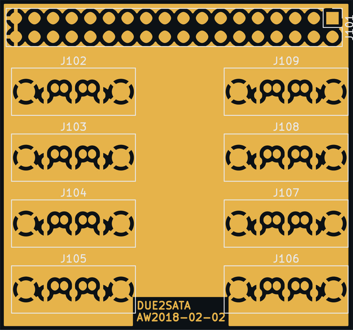
J101 designator is printed across the board edge (x 157.0-158.1 mm against an outline at 158.0 mm)
The rotated "J101" silk designator sits at the right-hand board edge and runs about 0.1 mm past the outline, so the routed edge will clip it or the fab will drop it.
Item Value Source Board outline, right edge x = 158.0 mm layout outlineRegion "J101" text extent x ~157.0 to ~158.1 mm, character height ~1.1 mm F.SILKSCREEN render at 122 px/mm, region x 150-158.2, y -66..-60 Copper pour edge ~157.6 mm F.CU render, same region Every other designator (J102-J109) is well inside the board and legible at ~1.2 mm. J101 is the only header and the one a user has to orient against the Arduino Due, so the label matters most there; pin 1 is still identifiable from the square pad and the silk corner box.
About this design
- Design
- RF MUX 8CH DUE2SATA — OHWR0072 R1
- Designed in
- KiCad EDA
- Board
- 2 copper layers, 48 × 45 mm, 9 components, 35 nets
- Licence
- CERN-OHL-1.2
- Source
- https://gitlab.com/ohwr/project/rf-mux-8ch at commit
c9a22e0867b6 - Attribution
- CERN Open Hardware Repository, project ohwr/project/rf-mux-8ch (commit c9a22e0867b6d2760bffcc8af0910b146cf221cb, 2025-04-10). Licence: CERN-OHL-1.2. Source: https://gitlab.com/ohwr/project/rf-mux-8ch. This is a snapshot of the copy published on the OHWR GitLab pages (R1), not CERN's released record. CERN's source of truth is EDMS (https://edms.cern.ch), and the current release may be newer.
- Reviewed with
- Probe by E# (E-Sharp AB)