 Probe

RF MUX 8CH
OHWR0071 · revision R1
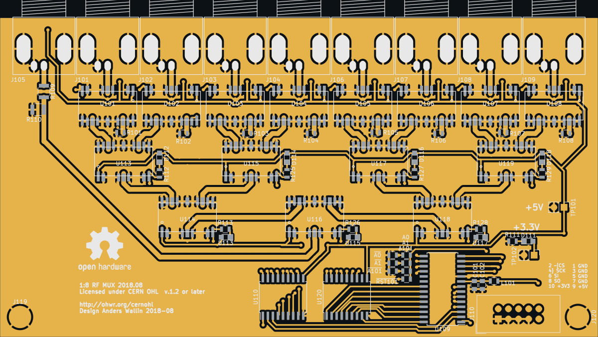
RF MUX 8CH (OHWR0071 R1) is an open-hardware circuit board from the CERN Open Hardware Repository, designed in KiCad EDA: a 2-layer board of 150 × 80 mm with 554 components and 94 nets, published under CERN-OHL-1.2.
review 96% walked · 8 findings: 3 major · 5 minor (24 items)
Open in the interactive viewerRead the full review
Design review
Probe recorded 8 findings: 3 major · 5 minor (24 items) on this design. Each is shown here with its reasoning; the full review links every one to the pins, nets and datasheet pages it rests on.
MCP23S17 U109 address straps: A0/~{A0}, A1/~{A1}, A101/~{A101} are all 0R in the layout, shorting +3V3VDC to GND three times
Conclusion
In the layout this board was ingested from (mux/rf_mux_8ch_v2.kicad_pcb), each MCP23S17 (U109) address pin has two strap resistors. One goes to +3V3VDC (A0, A1, A101) and one goes to GND (~{A0}, ~{A1}, ~{A101}). All six carry the value 0R, and none is marked do-not-place. Built as the layout states, each pair is a 0-ohm path from +3V3VDC to GND, so the 3.3 V supply from J110 pin 10 is shorted three times over.
The schematic (mux/rf_mux_8ch_v2.kicad_sch) populates these differently. It draws the same straps as R101/R103/R106 (to +3V3VDC, value DNI) and R102/R104/R107 (to GND, value 0R). That selects address 000, which matches the sheet note 'SPI ADDRESS BITS Software default is "000"'. The layout's values were never brought in line with that.
What sits between what
``
mermaid graph LR V33[+3V3VDC from J110.10] --> A0[A0 0R] --> N0[U109.15 A0] --> nA0[~A0 0R] --> G[GND] V33 --> A1[A1 0R] --> N1[U109.16 A1] --> nA1[~A1 0R] --> G V33 --> A2[A101 0R] --> N2[U109.17 A2] --> nA2[~A101 0R] --> G``Limit / actual / margin
Item Limit or intent Layout (as ingested) Margin Strap pair per address pin exactly one of the two fitted (the datasheet requires the pin to be externally biased) both fitted, 0R + 0R none: 0-ohm short from +3V3VDC to GND Pairs affected 0 3 (A0/~{A0}, A1/~{A1}, A101/~{A101}) Schematic population +3V3 side DNI, GND side 0R (address 000) all 0R layout values out of sync with the schematic Why it matters
The MCP23S17 datasheet requires the address pins to be biased even when hardware addressing is off (IOCON.HAEN = 0). A board assembled from the layout's values cannot power its 3.3 V domain; the controller's 3.3 V output on the IDC cable is shorted. The earlier layouts in mux/old (2018.11, 2020.09) mark all six straps DNI, which leaves A0-A2 floating, so none of the released layouts carries the schematic's population.
Fix
Mark A0, A1 and A101 (the +3V3VDC side) as DNP in the layout, or set their values to DNI to match the schematic.
- FiducialMissingmajorOpen
FiducialMissing: 2 boards×2
2 checked by the review by evaluation@esharp.se — 2 different reasons
At bottom, top
Each finding, with its own headline
bottomThe bottom side carries 18 SMT component(s) and no fiducial was found on it
The bottom side carries 18 SMT component(s) but no fiducial was found on it — a placement machine has no optical reference to align to. Probe found no pad labelled .pad_usage=g_fiducial/l_fiducial (basis pad_usage); no single-pad, netless, undrilled component whose 0.5-3 mm round pad has a concentric solder-mask opening at least 1.5x its diameter with no other copper inside it (basis geometry); and no component whose refdes starts FID or whose part or package name contains FIDUCIAL (basis footprint-name). If your library names fiducials something Probe does not recognise, mark this benign — disposition_finding(rule='FiducialMissing', entity='bottom', status='benign', reason=…) — the name match only ever silences this check, it never asserts anything. If the side really has no fiducial, say so with status='confirmed': that answers the finding and keeps it gating release.
topThe top side carries 35 SMT component(s) and no fiducial was found on it
The top side carries 35 SMT component(s) but no fiducial was found on it — a placement machine has no optical reference to align to. Probe found no pad labelled .pad_usage=g_fiducial/l_fiducial (basis pad_usage); no single-pad, netless, undrilled component whose 0.5-3 mm round pad has a concentric solder-mask opening at least 1.5x its diameter with no other copper inside it (basis geometry); and no component whose refdes starts FID or whose part or package name contains FIDUCIAL (basis footprint-name). If your library names fiducials something Probe does not recognise, mark this benign — disposition_finding(rule='FiducialMissing', entity='top', status='benign', reason=…) — the name match only ever silences this check, it never asserts anything. If the side really has no fiducial, say so with status='confirmed': that answers the finding and keeps it gating release.
- ReferencePlaneDiscontinuitymajorOpen
ReferencePlaneDiscontinuity: 16 boards×16
e.g. “'COL12' crosses where the outline of the GND plane on F.CU is drawn back, at 1 place, the longest 0.51 mm (fastest: COL12 at 100 ps 10-90 %, ASSUMED)” · 14 different statements
At nostitch:GND@B.CU|F.CU, void:GND@B.CU:152.39,-117.5, void:GND@F.CU:116.15,-86.15, void:GND@F.CU:125.5,-107.75, void:GND@F.CU:130.15,-76.38, void:GND@F.CU:160.75,-78 and 10 more
Each finding, with its own headline
nostitch:GND@B.CU|F.CU25 nets change between GND on B.CU and GND on F.CU at 29 vias, and no via of GND joins the two layers (fastest: /SI at 100 ps 10-90 %, ASSUMED)
29 via(s) take a signal from a layer referenced by GND on B.CU to one referenced by GND on F.CU, and no via of GND lands a pad on both layers (or spans them where the plane covers its drill), so nothing on the board carries the return from one to the other. One decision covers the pair of layers: stitch GND between them, or accept it for these nets.
- '/SCK' at (185, -107.5), F.CU -> B.CU: GND on B.CU and on F.CU; pure, no reference continues across
- '/SI' at (185.51, -106.02), F.CU -> B.CU: GND on B.CU and on F.CU; pure, no reference continues across
- '/SO' at (186, -105), F.CU -> B.CU: GND on B.CU and on F.CU; pure, no reference continues across
- '/~{CS}' at (184.05, -108.55), F.CU -> B.CU: GND on B.CU and on F.CU; pure, no reference continues across
- 'COL1' at (79, -63), F.CU -> B.CU: GND on B.CU and on F.CU; pure, no reference continues across
- 'COL1' at (125.5, -108.5), F.CU -> B.CU: GND on B.CU and on F.CU; pure, no reference continues across
- 'COL10' at (129.5, -87), F.CU -> B.CU: GND on B.CU and on F.CU; pure, no reference continues across
- 'COL10' at (133, -108.5), F.CU -> B.CU: GND on B.CU and on F.CU; pure, no reference continues across
- 'COL11' at (144.5, -108.5), F.CU -> B.CU: GND on B.CU and on F.CU; pure, no reference continues across
- 'COL12' at (148.5, -108.5), F.CU -> B.CU: GND on B.CU and on F.CU; pure, no reference continues across
- 'COL12' at (193.5, -87), F.CU -> B.CU: GND on B.CU and on F.CU; pure, no reference continues across
- 'COL13' at (129.5, -108.5), F.CU -> B.CU: GND on B.CU and on F.CU; pure, no reference continues across
- and 17 more
Every site is a row of this finding's evidence, keyed by net, layers and position. GET /api/odb/boards/72/reference-planes?group=nostitch%3AGND%40B.CU%7CF.CU serves each with its own layer_image region; all of them lie in x 77..195.5, y -124..-61 mm (board frame, Y up).
The reference on each layer is the first plane the track meets leaving the via, anti-pads and the net's own copper skipped. Whether it matters depends on each signal's edge rate, which nothing on file states for these nets: a slow static line crosses a split harmlessly, a fast edge does not.
void:GND@B.CU:152.39,-117.5'Net-(U109-Pad26)' crosses where the outline of the GND plane on B.CU is drawn back, at 1 place, the longest 5.83 mm (fastest: Net-(U109-Pad26) at 100 ps 10-90 %, ASSUMED)
Along 'Net-(U109-Pad26)' on F.CU, the GND plane on B.CU has 5.83 mm under the track with no copper, at (152.39, -117.5), the same plane on both sides. No single drill's anti-pad and no landing explains it: a clearance is excused only when it holds a drill and is drawn round it, or the track ends in it on the net's own pad or via, or runs through its own via's clearance and no farther. The return current detours round the void. 1 of them run ALONG the bare copper, parallel to its edges, rather than across it (the longest 5.23 mm). No hole cleared it: the outline of the pour at x 60.01..209.99, y -124.99..-45.01 is drawn back there. One decision covers the void: whether these tracks may cross it, or the plane should be filled under them. No crossing has a plane on the track's other side, so the whole return meets the break.
- 'Net-(U109-Pad26)' on F.CU at (152.39, -117.5), 5.83 mm, running ALONG the bare copper for 5.23 mm, not across it over no copper; other side: none: the signal layer is outermost
Every site is a row of this finding's evidence, keyed by net, layers and position. GET /api/odb/boards/72/reference-planes?group=void%3AGND%40B.CU%3A152.39%2C-117.5 serves each with its own layer_image region; all of them lie in x 148.56..156.21, y -118.71..-116.5 mm (board frame, Y up).
Read from the copper as drawn on the reference layer, along each track's centreline at exact breakpoints. The reference is the copper beside the track, never the layer's type or name. Whether it matters depends on each signal's edge rate, which nothing on file states for these nets: a slow static line crosses a split harmlessly, a fast edge does not.
void:GND@F.CU:116.15,-86.15'COL3' crosses where the outline of the GND plane on F.CU is drawn back, at 1 place, the longest 1.02 mm (fastest: COL3 at 100 ps 10-90 %, ASSUMED)
Along 'COL3' on B.CU, the GND plane on F.CU has 1.02 mm under the track with no copper, at (116.15, -86.15), the same plane on both sides. No single drill's anti-pad and no landing explains it: a clearance is excused only when it holds a drill and is drawn round it, or the track ends in it on the net's own pad or via, or runs through its own via's clearance and no farther. The return current detours round the void. No hole cleared it: the outline of the pour at x 60.01..209.99, y -124.99..-45.01 is drawn back there. One decision covers the void: whether these tracks may cross it, or the plane should be filled under them. No crossing has a plane on the track's other side, so the whole return meets the break.
- 'COL3' on B.CU at (116.15, -86.15), 1.02 mm over no copper; other side: none: the signal layer is outermost
Every site is a row of this finding's evidence, keyed by net, layers and position. GET /api/odb/boards/72/reference-planes?group=void%3AGND%40F.CU%3A116.15%2C-86.15 serves each with its own layer_image region; all of them lie in x 114.79..117.51, y -87.51..-84.79 mm (board frame, Y up).
Read from the copper as drawn on the reference layer, along each track's centreline at exact breakpoints. The reference is the copper beside the track, never the layer's type or name. Whether it matters depends on each signal's edge rate, which nothing on file states for these nets: a slow static line crosses a split harmlessly, a fast edge does not.
void:GND@F.CU:125.5,-107.75'COL2' crosses where the outline of the GND plane on F.CU is drawn back, at 1 place, the longest 1.04 mm (fastest: COL2 at 100 ps 10-90 %, ASSUMED)
Along 'COL2' on B.CU, the GND plane on F.CU has 1.04 mm under the track with no copper, at (125.5, -107.75), the same plane on both sides. No single drill's anti-pad and no landing explains it: a clearance is excused only when it holds a drill and is drawn round it, or the track ends in it on the net's own pad or via, or runs through its own via's clearance and no farther. The return current detours round the void. No hole cleared it: the outline of the pour at x 60.01..209.99, y -124.99..-45.01 is drawn back there. One decision covers the void: whether these tracks may cross it, or the plane should be filled under them. No crossing has a plane on the track's other side, so the whole return meets the break.
- 'COL2' on B.CU at (125.5, -107.75), 1.04 mm over no copper; other side: none: the signal layer is outermost
Every site is a row of this finding's evidence, keyed by net, layers and position. GET /api/odb/boards/72/reference-planes?group=void%3AGND%40F.CU%3A125.5%2C-107.75 serves each with its own layer_image region; all of them lie in x 123.98..127.02, y -108.75..-106.75 mm (board frame, Y up).
Read from the copper as drawn on the reference layer, along each track's centreline at exact breakpoints. The reference is the copper beside the track, never the layer's type or name. Whether it matters depends on each signal's edge rate, which nothing on file states for these nets: a slow static line crosses a split harmlessly, a fast edge does not.
void:GND@F.CU:130.15,-76.38'COL4' crosses where the outline of the GND plane on F.CU is drawn back, at 1 place, the longest 1.25 mm (fastest: COL4 at 100 ps 10-90 %, ASSUMED)
Along 'COL4' on B.CU, the GND plane on F.CU has 1.25 mm under the track with no copper, at (130.15, -76.38), the same plane on both sides. No single drill's anti-pad and no landing explains it: a clearance is excused only when it holds a drill and is drawn round it, or the track ends in it on the net's own pad or via, or runs through its own via's clearance and no farther. The return current detours round the void. 1 of them run ALONG the bare copper, parallel to its edges, rather than across it (the longest 0.92 mm). No hole cleared it: the outline of the pour at x 60.01..209.99, y -124.99..-45.01 is drawn back there. One decision covers the void: whether these tracks may cross it, or the plane should be filled under them. No crossing has a plane on the track's other side, so the whole return meets the break.
- 'COL4' on B.CU at (130.15, -76.38), 1.25 mm, running ALONG the bare copper for 0.92 mm, not across it over no copper; other side: none: the signal layer is outermost
Every site is a row of this finding's evidence, keyed by net, layers and position. GET /api/odb/boards/72/reference-planes?group=void%3AGND%40F.CU%3A130.15%2C-76.38 serves each with its own layer_image region; all of them lie in x 129.15..131.15, y -78..-74.75 mm (board frame, Y up).
Read from the copper as drawn on the reference layer, along each track's centreline at exact breakpoints. The reference is the copper beside the track, never the layer's type or name. Whether it matters depends on each signal's edge rate, which nothing on file states for these nets: a slow static line crosses a split harmlessly, a fast edge does not.
void:GND@F.CU:160.75,-78'COL6' crosses where the outline of the GND plane on F.CU is drawn back, at 1 place, the longest 1.07 mm (fastest: COL6 at 100 ps 10-90 %, ASSUMED)
Along 'COL6' on B.CU, the GND plane on F.CU has 1.07 mm under the track with no copper, at (160.75, -78), the same plane on both sides. No single drill's anti-pad and no landing explains it: a clearance is excused only when it holds a drill and is drawn round it, or the track ends in it on the net's own pad or via, or runs through its own via's clearance and no farther. The return current detours round the void. No hole cleared it: the outline of the pour at x 60.01..209.99, y -124.99..-45.01 is drawn back there. One decision covers the void: whether these tracks may cross it, or the plane should be filled under them. No crossing has a plane on the track's other side, so the whole return meets the break.
- 'COL6' on B.CU at (160.75, -78), 1.07 mm over no copper; other side: none: the signal layer is outermost
Every site is a row of this finding's evidence, keyed by net, layers and position. GET /api/odb/boards/72/reference-planes?group=void%3AGND%40F.CU%3A160.75%2C-78 serves each with its own layer_image region; all of them lie in x 159.5..162, y -79.61..-76.75 mm (board frame, Y up).
Read from the copper as drawn on the reference layer, along each track's centreline at exact breakpoints. The reference is the copper beside the track, never the layer's type or name. Whether it matters depends on each signal's edge rate, which nothing on file states for these nets: a slow static line crosses a split harmlessly, a fast edge does not.
void:GND@F.CU:162.15,-76.18'COL6' crosses where the outline of the GND plane on F.CU is drawn back, at 1 place, the longest 1.42 mm (fastest: COL6 at 100 ps 10-90 %, ASSUMED)
Along 'COL6' on B.CU, the GND plane on F.CU has 1.42 mm under the track with no copper, at (162.15, -76.18), the same plane on both sides. No single drill's anti-pad and no landing explains it: a clearance is excused only when it holds a drill and is drawn round it, or the track ends in it on the net's own pad or via, or runs through its own via's clearance and no farther. The return current detours round the void. 1 of them run ALONG the bare copper, parallel to its edges, rather than across it (the longest 0.55 mm). No hole cleared it: the outline of the pour at x 60.01..209.99, y -124.99..-45.01 is drawn back there. One decision covers the void: whether these tracks may cross it, or the plane should be filled under them. No crossing has a plane on the track's other side, so the whole return meets the break.
- 'COL6' on B.CU at (162.15, -76.18), 1.42 mm, running ALONG the bare copper for 0.55 mm, not across it over no copper; other side: none: the signal layer is outermost
Every site is a row of this finding's evidence, keyed by net, layers and position. GET /api/odb/boards/72/reference-planes?group=void%3AGND%40F.CU%3A162.15%2C-76.18 serves each with its own layer_image region; all of them lie in x 160.75..163.15, y -78..-74.75 mm (board frame, Y up).
Read from the copper as drawn on the reference layer, along each track's centreline at exact breakpoints. The reference is the copper beside the track, never the layer's type or name. Whether it matters depends on each signal's edge rate, which nothing on file states for these nets: a slow static line crosses a split harmlessly, a fast edge does not.
void:GND@F.CU:164.05,-92.5'COL12' crosses where the outline of the GND plane on F.CU is drawn back, at 1 place, the longest 0.51 mm (fastest: COL12 at 100 ps 10-90 %, ASSUMED)
Along 'COL12' on B.CU, the GND plane on F.CU has 0.51 mm under the track with no copper, at (164.05, -92.5), the same plane on both sides. No single drill's anti-pad and no landing explains it: a clearance is excused only when it holds a drill and is drawn round it, or the track ends in it on the net's own pad or via, or runs through its own via's clearance and no farther. The return current detours round the void. No hole cleared it: the outline of the pour at x 60.01..209.99, y -124.99..-45.01 is drawn back there. One decision covers the void: whether these tracks may cross it, or the plane should be filled under them. No crossing has a plane on the track's other side, so the whole return meets the break.
- 'COL12' on B.CU at (164.05, -92.5), 0.51 mm over no copper; other side: none: the signal layer is outermost
Every site is a row of this finding's evidence, keyed by net, layers and position. GET /api/odb/boards/72/reference-planes?group=void%3AGND%40F.CU%3A164.05%2C-92.5 serves each with its own layer_image region; all of them lie in x 162.79..165.3, y -93.5..-91.5 mm (board frame, Y up).
Read from the copper as drawn on the reference layer, along each track's centreline at exact breakpoints. The reference is the copper beside the track, never the layer's type or name. Whether it matters depends on each signal's edge rate, which nothing on file states for these nets: a slow static line crosses a split harmlessly, a fast edge does not.
void:GND@F.CU:165.34,-92.5'COL12' crosses where the outline of the GND plane on F.CU is drawn back, at 1 place, the longest 0.67 mm (fastest: COL12 at 100 ps 10-90 %, ASSUMED)
Along 'COL12' on B.CU, the GND plane on F.CU has 0.67 mm under the track with no copper, at (165.34, -92.5), the same plane on both sides. No single drill's anti-pad and no landing explains it: a clearance is excused only when it holds a drill and is drawn round it, or the track ends in it on the net's own pad or via, or runs through its own via's clearance and no farther. The return current detours round the void. No hole cleared it: the outline of the pour at x 60.01..209.99, y -124.99..-45.01 is drawn back there. One decision covers the void: whether these tracks may cross it, or the plane should be filled under them. No crossing has a plane on the track's other side, so the whole return meets the break.
- 'COL12' on B.CU at (165.34, -92.5), 0.67 mm over no copper; other side: none: the signal layer is outermost
Every site is a row of this finding's evidence, keyed by net, layers and position. GET /api/odb/boards/72/reference-planes?group=void%3AGND%40F.CU%3A165.34%2C-92.5 serves each with its own layer_image region; all of them lie in x 164..166.67, y -93.5..-91.5 mm (board frame, Y up).
Read from the copper as drawn on the reference layer, along each track's centreline at exact breakpoints. The reference is the copper beside the track, never the layer's type or name. Whether it matters depends on each signal's edge rate, which nothing on file states for these nets: a slow static line crosses a split harmlessly, a fast edge does not.
void:GND@F.CU:176.67,-92.5'COL12' crosses where the outline of the GND plane on F.CU is drawn back, at 1 place, the longest 0.67 mm (fastest: COL12 at 100 ps 10-90 %, ASSUMED)
Along 'COL12' on B.CU, the GND plane on F.CU has 0.67 mm under the track with no copper, at (176.67, -92.5), the same plane on both sides. No single drill's anti-pad and no landing explains it: a clearance is excused only when it holds a drill and is drawn round it, or the track ends in it on the net's own pad or via, or runs through its own via's clearance and no farther. The return current detours round the void. No hole cleared it: the outline of the pour at x 60.01..209.99, y -124.99..-45.01 is drawn back there. One decision covers the void: whether these tracks may cross it, or the plane should be filled under them. No crossing has a plane on the track's other side, so the whole return meets the break.
- 'COL12' on B.CU at (176.67, -92.5), 0.67 mm over no copper; other side: none: the signal layer is outermost
Every site is a row of this finding's evidence, keyed by net, layers and position. GET /api/odb/boards/72/reference-planes?group=void%3AGND%40F.CU%3A176.67%2C-92.5 serves each with its own layer_image region; all of them lie in x 175.33..178, y -93.5..-91.5 mm (board frame, Y up).
Read from the copper as drawn on the reference layer, along each track's centreline at exact breakpoints. The reference is the copper beside the track, never the layer's type or name. Whether it matters depends on each signal's edge rate, which nothing on file states for these nets: a slow static line crosses a split harmlessly, a fast edge does not.
void:GND@F.CU:177.96,-92.5'COL12' crosses where the outline of the GND plane on F.CU is drawn back, at 1 place, the longest 0.51 mm (fastest: COL12 at 100 ps 10-90 %, ASSUMED)
Along 'COL12' on B.CU, the GND plane on F.CU has 0.51 mm under the track with no copper, at (177.96, -92.5), the same plane on both sides. No single drill's anti-pad and no landing explains it: a clearance is excused only when it holds a drill and is drawn round it, or the track ends in it on the net's own pad or via, or runs through its own via's clearance and no farther. The return current detours round the void. No hole cleared it: the outline of the pour at x 60.01..209.99, y -124.99..-45.01 is drawn back there. One decision covers the void: whether these tracks may cross it, or the plane should be filled under them. No crossing has a plane on the track's other side, so the whole return meets the break.
- 'COL12' on B.CU at (177.96, -92.5), 0.51 mm over no copper; other side: none: the signal layer is outermost
Every site is a row of this finding's evidence, keyed by net, layers and position. GET /api/odb/boards/72/reference-planes?group=void%3AGND%40F.CU%3A177.96%2C-92.5 serves each with its own layer_image region; all of them lie in x 176.7..179.21, y -93.5..-91.5 mm (board frame, Y up).
Read from the copper as drawn on the reference layer, along each track's centreline at exact breakpoints. The reference is the copper beside the track, never the layer's type or name. Whether it matters depends on each signal's edge rate, which nothing on file states for these nets: a slow static line crosses a split harmlessly, a fast edge does not.
void:GND@F.CU:189.16,-78.34'COL8' crosses where the outline of the GND plane on F.CU is drawn back, at 1 place, the longest 0.38 mm (fastest: COL8 at 100 ps 10-90 %, ASSUMED)
Along 'COL8' on B.CU, the GND plane on F.CU has 0.38 mm under the track with no copper, at (189.16, -78.34), the same plane on both sides. No single drill's anti-pad and no landing explains it: a clearance is excused only when it holds a drill and is drawn round it, or the track ends in it on the net's own pad or via, or runs through its own via's clearance and no farther. The return current detours round the void. No hole cleared it: the outline of the pour at x 60.01..209.99, y -124.99..-45.01 is drawn back there. One decision covers the void: whether these tracks may cross it, or the plane should be filled under them. No crossing has a plane on the track's other side, so the whole return meets the break.
- 'COL8' on B.CU at (189.16, -78.34), 0.38 mm over no copper; other side: none: the signal layer is outermost
Every site is a row of this finding's evidence, keyed by net, layers and position. GET /api/odb/boards/72/reference-planes?group=void%3AGND%40F.CU%3A189.16%2C-78.34 serves each with its own layer_image region; all of them lie in x 188.02..190.29, y -79.48..-77.21 mm (board frame, Y up).
Read from the copper as drawn on the reference layer, along each track's centreline at exact breakpoints. The reference is the copper beside the track, never the layer's type or name. Whether it matters depends on each signal's edge rate, which nothing on file states for these nets: a slow static line crosses a split harmlessly, a fast edge does not.
void:GND@F.CU:95.25,-85.79'COL2' crosses where the outline of the GND plane on F.CU is drawn back, at 1 place, the longest 1.09 mm (fastest: COL2 at 100 ps 10-90 %, ASSUMED)
Along 'COL2' on B.CU, the GND plane on F.CU has 1.09 mm under the track with no copper, at (95.25, -85.79), the same plane on both sides. No single drill's anti-pad and no landing explains it: a clearance is excused only when it holds a drill and is drawn round it, or the track ends in it on the net's own pad or via, or runs through its own via's clearance and no farther. The return current detours round the void. 1 of them run ALONG the bare copper, parallel to its edges, rather than across it (the longest 0.71 mm). No hole cleared it: the outline of the pour at x 60.01..209.99, y -124.99..-45.01 is drawn back there. One decision covers the void: whether these tracks may cross it, or the plane should be filled under them. No crossing has a plane on the track's other side, so the whole return meets the break.
- 'COL2' on B.CU at (95.25, -85.79), 1.09 mm, running ALONG the bare copper for 0.71 mm, not across it over no copper; other side: none: the signal layer is outermost
Every site is a row of this finding's evidence, keyed by net, layers and position. GET /api/odb/boards/72/reference-planes?group=void%3AGND%40F.CU%3A95.25%2C-85.79 serves each with its own layer_image region; all of them lie in x 94.25..96.25, y -87.34..-84.25 mm (board frame, Y up).
Read from the copper as drawn on the reference layer, along each track's centreline at exact breakpoints. The reference is the copper beside the track, never the layer's type or name. Whether it matters depends on each signal's edge rate, which nothing on file states for these nets: a slow static line crosses a split harmlessly, a fast edge does not.
void:GND@F.CU:copper of +3V3VDC'/~{CS}' crosses where the GND plane on F.CU is drawn back round copper of +3V3VDC, at 1 place, the longest 2.32 mm (fastest: /~{CS} at 100 ps 10-90 %, ASSUMED)
Along '/~{CS}' on B.CU, the GND plane on F.CU has 2.32 mm under the track with copper of +3V3VDC, not a plane, at (185, -111), the same plane on both sides. No single drill's anti-pad and no landing explains it: a clearance is excused only when it holds a drill and is drawn round it, or the track ends in it on the net's own pad or via, or runs through its own via's clearance and no farther. The return current detours round the void. 1 of them run ALONG the bare copper, parallel to its edges, rather than across it (the longest 1.3 mm). No hole cleared it: the outline of the pour at x 60.01..209.99, y -124.99..-45.01 is drawn back there. One decision covers the void: whether these tracks may cross it, or the plane should be filled under them. No crossing has a plane on the track's other side, so the whole return meets the break.
- '/~{CS}' on B.CU at (185, -111), 2.32 mm, running ALONG the bare copper for 1.3 mm, not across it over copper of +3V3VDC, not a plane; other side: none: the signal layer is outermost
Every site is a row of this finding's evidence, keyed by net, layers and position. GET /api/odb/boards/72/reference-planes?group=void%3AGND%40F.CU%3Acopper%20of%20%2B3V3VDC serves each with its own layer_image region; all of them lie in x 184..186, y -113.16..-108.84 mm (board frame, Y up).
Read from the copper as drawn on the reference layer, along each track's centreline at exact breakpoints. The reference is the copper beside the track, never the layer's type or name. Whether it matters depends on each signal's edge rate, which nothing on file states for these nets: a slow static line crosses a split harmlessly, a fast edge does not.
void:GND@F.CU:relief'COL2' crosses the thermal reliefs of the GND plane on F.CU at 1 place, the longest 1.15 mm (fastest: COL2 at 100 ps 10-90 %, ASSUMED)
The GND plane on F.CU is drawn back round copper of its own net - pads spoked into it, in thermal reliefs - and tracks cross those reliefs: over the bare ring either side of the pad or spoke the return has no plane under it, and finds its way round through the spokes. 1 place(s) on 1 net(s), each the relief's bare stretches either side of that copper counted together, the longest 1.15 mm. One decision covers the pour's reliefs: whether tracks may cross them, or the reliefs or the routing should keep them apart. No crossing has a plane on the track's other side, so the whole return meets the break.
- 'COL2' on B.CU at (95.44, -84.46), 1.15 mm, running ALONG the bare copper for 0.61 mm, not across it over no copper; other side: none: the signal layer is outermost
Every site is a row of this finding's evidence, keyed by net, layers and position. GET /api/odb/boards/72/reference-planes?group=void%3AGND%40F.CU%3Arelief serves each with its own layer_image region; all of them lie in x 94.25..96.65, y -85.75..-82.49 mm (board frame, Y up).
Read from the copper as drawn on the reference layer, along each track's centreline at exact breakpoints. The reference is the copper beside the track, never the layer's type or name. Whether it matters depends on each signal's edge rate, which nothing on file states for these nets: a slow static line crosses a split harmlessly, a fast edge does not.
void:routed@B.CU|F.CUTracks on B.CU and F.CU cross each other at 59 places, each layer the other's reference with its pour cleared round its own tracks, the longest 42.42 mm; 24 run ALONG the cut round another net's track (fastest: /SI at 100 ps 10-90 %, ASSUMED)
B.CU and F.CU each carry a pour and routed tracks, and each is the other's nearest reference. Wherever a track on one crosses a track on the other, the pour under it is cleared round that other track, so for the width of the cut the return has no plane under it and detours round the cut. 59 place(s) on 41 net(s), 24 of them seen from both tracks (each counted once). 24 of the crossings run ALONG the cut round another net's track rather than across it, parallel to its edges (the longest 40.41 mm): over or right beside that track, broadside to it as well as off the plane. One decision covers the layer pair: whether these layers may take a pour their own tracks cut as the reference, or the routing or the stackup should give the tracks a plane that is not cut where they cross. No crossing has a plane on the track's other side, so the whole return meets the break.
- one crossing of two tracks, seen from each: 'Net-(U109-Pad1)' on B.CU at (146.65, -123.5), 42.41 mm, running ALONG the bare copper for 40.14 mm, not across it over copper of Net-(U109-Pad2), not a plane; other side: none: the signal layer is outermost / 'Net-(U109-Pad2)' on F.CU at (146.8, -123), 42.42 mm, running ALONG the bare copper for 40.41 mm, not across it over copper of Net-(U109-Pad1), not a plane; other side: none: the signal layer is outermost
- one crossing of two tracks, seen from each: 'Net-(U109-Pad21)' on F.CU at (156.38, -112.36), 26.01 mm, running ALONG the bare copper for 18.45 mm, not across it over copper of Net-(U109-Pad8), Net-(U109-Pad4), Net-(U109-Pad5), Net-(U109-Pad6), Net-(U109-Pad7), not a plane, to the end of the track; other side: none: the signal layer is outermost / 'Net-(U109-Pad22)' on F.CU at (156.79, -113.63), 23.38 mm, running ALONG the bare copper for 17.62 mm, not across it over copper of Net-(U109-Pad4), Net-(U109-Pad5), Net-(U109-Pad6), Net-(U109-Pad7), not a plane, to the end of the track; other side: none: the signal layer is outermost / 'Net-(U109-Pad23)' on F.CU at (156.66, -114.91), 21.84 mm, running ALONG the bare copper for 17.88 mm, not across it over copper of Net-(U109-Pad6), Net-(U109-Pad4), Net-(U109-Pad5), not a plane, to the end of the track; other side: none: the signal layer is outermost / 'Net-(U109-Pad24)' on F.CU at (156.38, -116.17), 20.62 mm, running ALONG the bare copper for 18.45 mm, not across it over copper of Net-(U109-Pad5), Net-(U109-Pad4), not a plane, to the end of the track; other side: none: the signal layer is outermost / 'Net-(U109-Pad25)' on F.CU at (161.43, -117.44), 19.24 mm, running ALONG the bare copper for 17.44 mm, not across it over copper of Net-(U109-Pad4), not a plane, to the end of the track; other side: none: the signal layer is outermost / 'Net-(U109-Pad4)' on B.CU at (162.03, -117), 25.57 mm, running ALONG the bare copper for 18.06 mm, not across it over copper of Net-(U109-Pad25), Net-(U109-Pad24), Net-(U109-Pad23), Net-(U109-Pad22), Net-(U109-Pad21), not a plane; other side: none: the signal layer is outermost / 'Net-(U109-Pad5)' on B.CU at (156.38, -116), 24.59 mm, running ALONG the bare copper for 19.59 mm, not across it over copper of Net-(U109-Pad24), Net-(U109-Pad23), Net-(U109-Pad22), Net-(U109-Pad21), not a plane; other side: none: the signal layer is outermost / 'Net-(U109-Pad6)' on B.CU at (156.66, -115), 23.59 mm, running ALONG the bare copper for 18.89 mm, not across it over copper of Net-(U109-Pad23), Net-(U109-Pad22), Net-(U109-Pad21), not a plane; other side: none: the signal layer is outermost / 'Net-(U109-Pad7)' on B.CU at (158.2, -114), 22.6 mm, running ALONG the bare copper for 18 mm, not across it over copper of Net-(U109-Pad22), Net-(U109-Pad21), not a plane; other side: none: the signal layer is outermost / 'Net-(U109-Pad8)' on B.CU at (156.38, -112.5), 21.1 mm, running ALONG the bare copper for 19.55 mm, not across it over copper of Net-(U109-Pad21), not a plane; other side: none: the signal layer is outermost
- 'COL14' on B.CU at (170.85, -101.5), 23.52 mm, running ALONG the bare copper for 21.5 mm, not across it over copper of +5VDC, not a plane, to the end of the track; other side: none: the signal layer is outermost
- 'COL13' on B.CU at (121, -102.5), 13.81 mm, running ALONG the bare copper for 12 mm, not across it over copper of +5VDC, not a plane, to the end of the track; other side: none: the signal layer is outermost
- 'COL5' on B.CU at (140.48, -106.02), 8.84 mm, running ALONG the bare copper for 6.22 mm, not across it over copper of +5VDC, not a plane; other side: none: the signal layer is outermost
- one crossing of two tracks, seen from each: 'COL4' on B.CU at (130.15, -71), 5.39 mm, running ALONG the bare copper for 2.35 mm, not across it over copper of GND, Net-(U104-Pad14), not a plane; other side: none: the signal layer is outermost / 'Net-(U104-Pad14)' on F.CU at (130.61, -73.11), 1.9 mm over copper of COL4, not a plane; other side: none: the signal layer is outermost
- one crossing of two tracks, seen from each: 'COL6' on B.CU at (162.15, -71), 5.39 mm, running ALONG the bare copper for 2 mm, not across it over copper of Net-(U106-Pad14), GND, not a plane; other side: none: the signal layer is outermost / 'Net-(U106-Pad14)' on F.CU at (162.61, -73.11), 1.9 mm over copper of COL6, not a plane; other side: none: the signal layer is outermost
- one crossing of two tracks, seen from each: 'Net-(U109-Pad4)' on B.CU at (131.75, -117), 5.31 mm over copper of Net-(U109-Pad8), Net-(U109-Pad7), Net-(U109-Pad6), Net-(U109-Pad5), not a plane, to the end of the track; other side: none: the signal layer is outermost / 'Net-(U109-Pad5)' on B.CU at (134.27, -116), 4.31 mm over copper of Net-(U109-Pad8), Net-(U109-Pad7), Net-(U109-Pad6), not a plane, to the end of the track; other side: none: the signal layer is outermost / 'Net-(U109-Pad5)' on F.CU at (131, -117.46), 1.31 mm over copper of Net-(U109-Pad4), not a plane, to the end of the track; other side: none: the signal layer is outermost / 'Net-(U109-Pad6)' on B.CU at (134.27, -115), 2.81 mm over copper of Net-(U109-Pad8), Net-(U109-Pad7), not a plane, to the end of the track; other side: none: the signal layer is outermost / 'Net-(U109-Pad6)' on F.CU at (132.5, -116.5), 2.31 mm over copper of Net-(U109-Pad5), Net-(U109-Pad4), not a plane, to the end of the track; other side: none: the signal layer is outermost / 'Net-(U109-Pad7)' on B.CU at (135.46, -114), 1.31 mm over copper of Net-(U109-Pad8), not a plane, to the end of the track; other side: none: the signal layer is outermost / 'Net-(U109-Pad7)' on F.CU at (133.54, -115.5), 3.53 mm, running ALONG the bare copper for 1.26 mm, not across it over copper of Net-(U109-Pad6), Net-(U109-Pad5), Net-(U109-Pad4), not a plane, to the end of the track; other side: none: the signal layer is outermost / 'Net-(U109-Pad8)' on F.CU at (135, -114.5), 4.31 mm over copper of Net-(U109-Pad7), Net-(U109-Pad6), Net-(U109-Pad5), Net-(U109-Pad4), not a plane, to the end of the track; other side: none: the signal layer is outermost
- one crossing of two tracks, seen from each: 'COL2' on B.CU at (95.65, -77.11), 5.28 mm, running ALONG the bare copper for 2.15 mm, not across it over copper of Net-(U102-Pad14), not a plane; other side: none: the signal layer is outermost / 'Net-(U102-Pad14)' on F.CU at (95.07, -75.22), 1.43 mm over copper of COL2, not a plane; other side: none: the signal layer is outermost
- one crossing of two tracks, seen from each: 'COL6' on B.CU at (148.35, -101.15), 5.25 mm over copper of Net-(D115-Pad1), +5VDC, not a plane; other side: none: the signal layer is outermost / 'Net-(D115-Pad1)' on F.CU at (149.4, -99.45), 0.99 mm over copper of COL6, not a plane, to the end of the track; other side: none: the signal layer is outermost
- 'COL4' on B.CU at (130.15, -78.48), 5.15 mm, running ALONG the bare copper for 2.68 mm, not across it over copper of +5VDC, not a plane; other side: none: the signal layer is outermost
- one crossing of two tracks, seen from each: 'COL8' on B.CU at (191, -74.96), 4.92 mm over copper of Net-(U108-Pad14), GND, not a plane, to the end of the track; other side: none: the signal layer is outermost / 'Net-(U108-Pad14)' on F.CU at (191.51, -74.5), 3.84 mm, running ALONG the bare copper for 1.15 mm, not across it over copper of COL8, not a plane; other side: none: the signal layer is outermost
- and 47 more
Every site is a row of this finding's evidence, keyed by net, layers and position. GET /api/odb/boards/72/reference-planes?group=void%3Arouted%40B.CU%7CF.CU serves each with its own layer_image region; all of them lie in x 77.29..193.62, y -124.5..-60.92 mm (board frame, Y up).
Read from the copper as drawn on the reference layer, along each track's centreline at exact breakpoints. The reference is the copper beside the track, never the layer's type or name. Whether it matters depends on each signal's edge rate, which nothing on file states for these nets: a slow static line crosses a split harmlessly, a fast edge does not.
RF relay U102 (channel 2 input): layout net Net-(U102-Pad21) isolates pins 21/22 from GND, unlike the schematic and the other 14 HF3 relays
Conclusion
The ingested layout (mux/rf_mux_8ch_v2.kicad_pcb) has a net, Net-(U102-Pad21), that joins pads 21 and 22 of relay U102 (TE HF3, the channel-2 input relay behind BNC J102) and nothing else. It is one short F.Cu trace between the two pads. The schematic puts both pins on GND, and every other HF3 relay on the board has pins 21 and 22 on GND in the layout (U101, U103-U108, U113-U119). The two layouts in mux/old (2018.11, 2020.09) have no such net either. The layout and the schematic disagree here, and U102 is the only relay affected.
What sits between what
``
mermaid flowchart LR subgraph L["Layout"] P21["U102.21"] --- T["0.4 mm trace, Net-(U102-Pad21)"] --- P22["U102.22"] end GND["GND: pins 21/22 of the other 14 relays"] -. "no connection" .- P21``Limit / actual / margin
Item Schematic Layout Margin U102.21 GND Net-(U102-Pad21) not joined to GND U102.22 GND Net-(U102-Pad21) not joined to GND Pins 21/22 on the other relays GND GND (14 of 14) - Impact
The designer's symbol names these pins GND. If they are RF grounds of the 50-ohm relay, as that name suggests, channel 2 may show poorer return loss or isolation than the other seven channels. What is on file cannot confirm or size this: the only TE document held for the HF3 (1462051-2) is the dimensional customer drawing, which numbers pins 21 and 22 but does not state their function. The TE HF3 datasheet is needed.
Fix
Re-sync the layout from the schematic so that U102 pads 21 and 22 join GND.
No fiducials on either side, although both sides carry SMD parts (54 top, 18 bottom)
Conclusion
The layout has no fiducial on either side: no fiducial footprint, no pad flagged as one, and no bare-copper fiducial in the render. Both sides still need machine placement of SMD parts:
Side SMD placements Finest pitch Fiducials Top 54: 39 footprints with attr smd (U109 SOIC-28W, U110/U120 SOIC-18W, 0805 passives and LEDs) plus the 15 HF3 relays, whose pads are SMD although the footprint attribute says through_hole 1.27 mm 0 Bottom 18 (D101-D109 0805 LEDs, R114-R117, R120-R124 0805) 0805 0 ``
mermaid graph LR PnP[pick-and-place vision] -->|needs| F[global fiducials per side, or panel fiducials] F -.absent on board.- B[board top and bottom]``Risk
Without fiducials, automated placement has to align on board edges or tooling holes, or on fiducials the assembler adds to a panel frame. The pitches here (1.27 mm SOIC, 0805, HF3 gull-wing) tolerate that better than fine-pitch parts, so this is a minor manufacturability point rather than a functional one. It becomes a real problem only if the board is assembled as a single, unpanelised piece.
Fix
Add three global fiducials per side, or state in the fabrication notes that panel fiducials are to be used.
Schematic and layout are different revisions (schematic Rev 2018.11 with 2020-09 changes; layout and silkscreen 2018.08), and the schematic title block has no date
Conclusion
The files published as the current design do not describe the same revision:
File Title / revision Date mux/rf_mux_8ch_v2.kicad_sch (sheet 1 of 1) "1:8 RF Multiplexer - 2018.11", Rev 2018.11; revision notes up to "2020-09: optional SMA-connectors" empty mux/rf_mux_8ch_v2.kicad_pcb (the layout ingested here) "1:8 RF Multiplexer - 2018.08"; silkscreen "1:8 RF MUX 2018.08" 2018-02-06 The two also differ in content. The schematic has the SMA option connectors J111-J119 and relay K1 (HF3-53); the layout has U116 and no SMA footprints. The address straps are R101-R107 in the schematic and A0/~{A0} etc. in the layout, and the terminations are 49R9 in the schematic against 50R in the layout. Two electrical consequences are filed separately: OBS-150 (address-strap values) and OBS-151 (U102 pins 21/22).
``
mermaid graph LR SCH[schematic Rev 2018.11 + 2020-09 notes] -. not in sync .- PCB[layout 2018.08] PCB --> FAB[fabrication/assembly data]``Risk
Someone building from the repository cannot tell which schematic matches the layout, and the empty date field gives no tie-breaker. A BOM generated from one file and assembly data from the other gives different populations, and that is how the address-strap short in OBS-150 arises.
Fix
Update the layout from the schematic (or tag matching pairs), and fill in the schematic date and a revision that matches the layout's title block and silkscreen.
Silkscreen body outline of all 15 HF3 relay footprints (U101-U108, U113-U119) runs across every relay pad
Conclusion
The custom footprint awallinKiCadFootprints:SPDT_TE_HF3 draws its F.SilkS body rectangle at y = +/-3.6 mm, exactly the 7.2 mm housing width on TE drawing 1462051-2. Its SMD pads are centred at y = +/-3.0 mm and are 2.0-2.5 mm long, spanning about 2.0 to 4.0 mm. The 0.15 mm silk line therefore crosses every pad of every relay: 16 pads on each of the 15 placements U101-U108 and U113-U119, 240 pads in all. The layout's plot settings have subtractmaskfromsilk = false, so the design does not ask for silk to be clipped from the mask openings. The ODB++ that Probe renders shows the ink across the pads.
Where
Item Value Silk line (footprint frame) y = +/-3.6 mm, 0.15 mm stroke (= housing edge, 7.2 mm per TE 1462051-2) Pad extent (footprint frame) y about 2.0-4.0 mm (pads 0.7/0.9 x 2.0-2.5 mm at y = +/-3.0) Overlap the line lies inside every pad, about 0.6 mm from its inner end Placements U101, U102, U103, U104, U105, U106, U107, U108, U113, U114, U115, U116, U117, U118, U119 ``
mermaid graph TB S[F.SilkS body rectangle y=+/-3.6 mm = housing edge] -->|crosses| P[relay SMD pads y 2.0..4.0 mm] P --> J[solder joints of the RF contacts and coil]``Risk
Silk ink on a pad can stop paste wetting across the whole pad or lift the part slightly. On these relays that includes the RF COM/NO/NC pads and the ground pads. Many fabs clip silk from pads by default and the defect then never reaches copper, but the design data does not ask for it.
Fix
Move the footprint's body outline outside the pad rows (for example y = +/-4.2 mm), or draw it only between the pad groups, and enable silk clipping at plot.
Reference designators of all 15 HF3 relays (U101-U108, U113-U119) are printed inside the relay body outline and are hidden once the relays are fitted
Conclusion
The SPDT_TE_HF3 footprint places its reference text at the footprint centre, (0, 0.5) mm, on F.SilkS. That is inside the 14.6 x 7.2 mm body rectangle, and the relay housing covers it. On the assembled board none of the 15 relay designators can be read: U101-U108 (input relays) and U113-U119 (tree relays). All other designators on the top side sit outside their parts and measure 1.0 mm cap height with a 0.15 mm stroke, which is printable.
Placement group Designator position Visible after assembly U101-U108, U113-U119 (HF3 relays) footprint centre, inside the body outline no Other top-side parts (SOIC, 0805, BNC, headers) beside the part, 1.0 mm / 0.15 mm yes ``
mermaid graph LR T[refdes text at footprint centre] --> B[under the relay housing] B --> X[not readable after assembly or during rework]``Risk
Fault-finding and rework on an assembled board, for example replacing one relay of the 15 or probing a channel, has to rely on the assembly drawing rather than the board. The 15 relays look identical, and their tree position (input relays U101-U108, tree relays U113-U119) is what an engineer needs to identify.
Fix
Move the relay designators outside the body outline, for example between the relay rows.
Main parts
| Part number | Maker | Description | Where |
|---|---|---|---|
| MCP23S17 | U109 | ||
| ULN2803A | U110, U120 |
About this design
- Design
- RF MUX 8CH — OHWR0071 R1
- Designed in
- KiCad EDA
- Board
- 2 copper layers, 150 × 80 mm, 554 components, 94 nets
- Licence
- CERN-OHL-1.2
- Source
- https://gitlab.com/ohwr/project/rf-mux-8ch at commit
c9a22e0867b6 - Attribution
- CERN Open Hardware Repository, project ohwr/project/rf-mux-8ch (commit c9a22e0867b6d2760bffcc8af0910b146cf221cb, 2025-04-10). Licence: CERN-OHL-1.2. Source: https://gitlab.com/ohwr/project/rf-mux-8ch. This is a snapshot of the copy published on the OHWR GitLab pages (R1), not CERN's released record. CERN's source of truth is EDMS (https://edms.cern.ch), and the current release may be newer.
- Reviewed with
- Probe by E# (E-Sharp AB)