 Probe

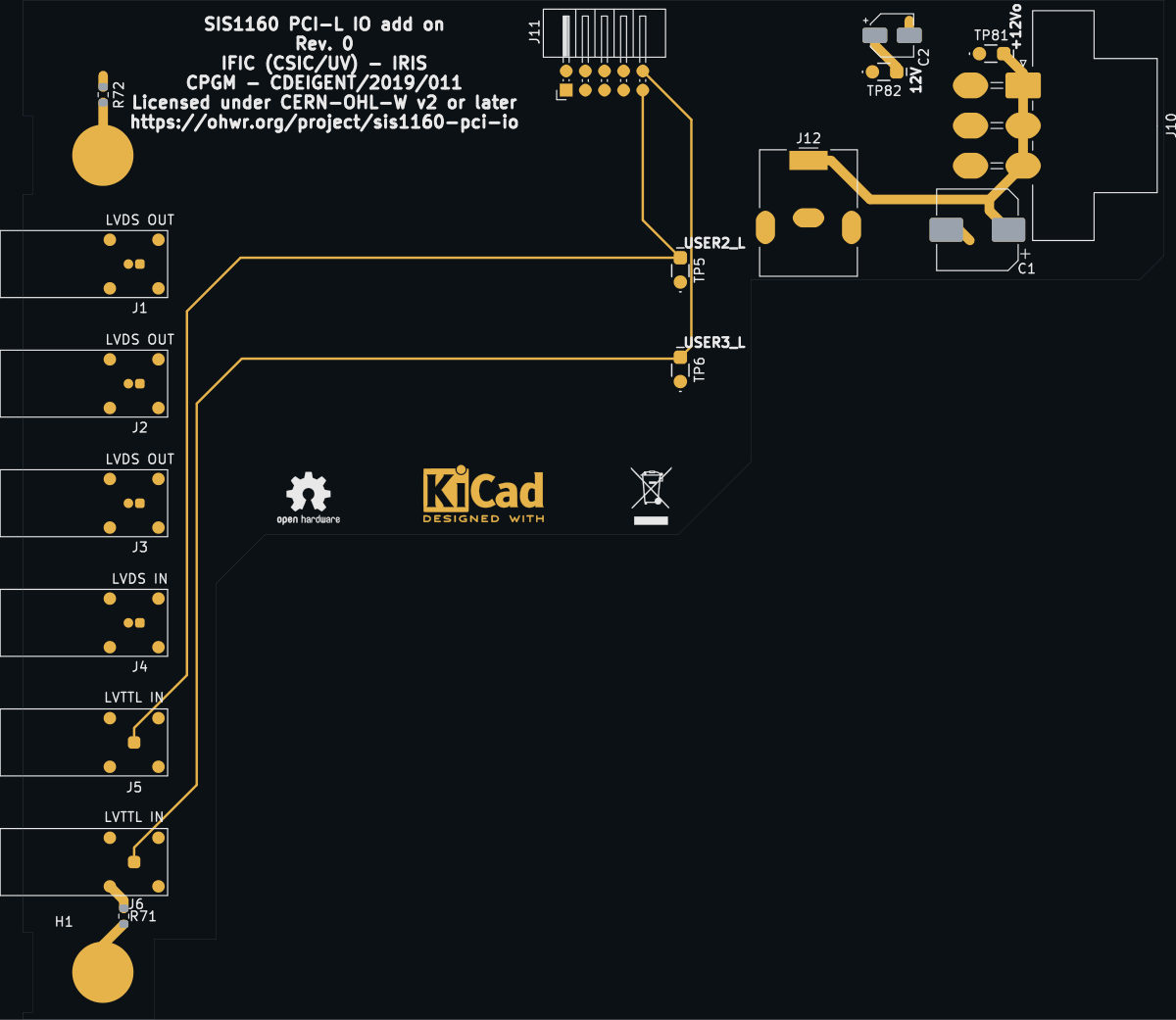
SIS1160 PCI IO
OHWR0080 · revision R1
SIS1160 PCI IO (OHWR0080 R1) is an open-hardware circuit board from the CERN Open Hardware Repository, designed in KiCad EDA: a 4-layer board of 119.3 × 106.6 mm with 21 components and 18 nets, published under CERN-OHL-W-2.0.
review complete · 7 findings: 1 blocker · 2 major · 4 minor (10 items)
Open in the interactive viewerRead the full review
Design review
Probe recorded 7 findings: 1 blocker · 2 major · 4 minor (10 items) on this design. Each is shown here with its reasoning; the full review links every one to the pins, nets and datasheet pages it rests on.
- NetCopperSplitblockerOpen
NetCopperSplit: 2 boards×2
e.g. “GND's copper is in 2 pieces: R71.2 is not connected to the rest of the net” · 2 different statements
At split:/MP, split:GND
Each finding, with its own headline
split:/MP/MP's copper is in 2 pieces: R71.1 is not connected to the rest of the net
/MP's copper is in 2 pieces: R71.1 is not connected to the rest of the net. Piece 1: H1.MP and R72.1, on F.CU, IN1.CU, IN2.CU and B.CU, 1 drill(s), over (1.42, -3.2) to (11.68, 91.43). Piece 2: R71.1, on F.CU, over (5.28, -3.2) to (11.68, 5.53). The export files every one of these pins under the net, so every connectivity check passes; the copper the fab builds leaves them apart. Usually a pour island that touches only one via of its own net, or a track ending short of its copper: join the piece to the net and export again.
split:GNDGND's copper is in 2 pieces: R71.2 is not connected to the rest of the net
GND's copper is in 2 pieces: R71.2 is not connected to the rest of the net. Piece 1: C1.2, C2.2, J1.3, J10.4, J10.6, J12.2, J12.MP, J2.3 and 10 more pin(s), on F.CU, IN1.CU, IN2.CU and B.CU, 17 drill(s), 5834.37 mm2 of pour, over (1.52, 3.56) to (119.35, 101.35). Piece 2: R71.2, on F.CU, over (8.56, 6.15) to (11.17, 9.63). The export files every one of these pins under the net, so every connectivity check passes; the copper the fab builds leaves them apart. Usually a pour island that touches only one via of its own net, or a track ending short of its copper: join the piece to the net and export again.
- CapVoltageDeratingmajorOpen
CapVoltageDerating: 2 components×2
2 checked by the review by Claude walker W4 (Cern session) — 2 different reasons
At C1, C2
Each finding, with its own headline
C1C1 sits on a 12 V rail and its voltage rating is not in the BOM
C1: on a 12 V rail but its voltage rating is not stated in the BOM — add it so the rating can be compared to the rail at all. No datasheet is on file for this part; the BOM short-spec is the source.
C2C2 sits on a 12 V rail and its voltage rating is not in the BOM
C2: on a 12 V rail but its voltage rating is not stated in the BOM — add it so the rating can be compared to the rail at all. No datasheet is on file for this part; the BOM short-spec is the source.
- PartLifecyclemajorOpen
IRLML5203 on Q1: the distributor catalogue reports "Obsolete" for Infineon Technologies's IRLML5203
IRLML5203 on Q1: the distributor catalogue reports "Obsolete" for Infineon Technologies's IRLML5203 — a sourcing/longevity risk to confirm against the MANUFACTURER before acting. This board's BOM names no manufacturer for it, so whether that is the fitted maker's product was not checked. A distributor delisting is not the same claim as the part being unavailable; check the vendor's own lifecycle/product-change notice for the status and any named successor. Re-read the source: GET /api/odb/parts/IRLML5203/providers (which provider said it, the maker and part number it matched, its own words, and when we asked). No approved alternate is recorded for this position.
At Q1
C1 (470 uF polarised electrolytic) sits before the Q1 reverse-polarity MOSFET, so a reversed DC jack J12 reverse-biases it
The 470 uF polarised electrolytic C1 sits on the input side of the reverse-polarity MOSFET Q1, so a reversed supply on the DC jack J12 reverse-biases the very part the protection should cover.
Where it is
``
mermaid flowchart LR J10["J10 PEG 6-pin, keyed<br/>pins 1-3"] --> N["PEG+12Vo"] J12["J12 DC jack, centre pin 1<br/>alternative power supply connector"] --> N N --> C1["C1 470 uF 16 V<br/>polarised electrolytic"] N -- "Q1 drain" --> Q1["Q1 IRLML5203 P-MOSFET<br/>gate via R73 100k to GND"] Q1 -- "source, /12Vs" --> FB1["FB1"] --> P["+12V<br/>C2, TP82"]``- Q1 is the board's reverse-polarity protection; the schematic links a Verpolschutz (reverse-polarity protection) reference, lothar-miller.de.
- C1 is a Nichicon UWT1C471MNL1GS polarised aluminium electrolytic (CP_Elec_8x10 footprint), drawn on PEG+12Vo under DECOUPLING on sheet 1 (BoardIO.kicad_sch).
Why it matters
If a centre-negative adaptor is plugged into J12, Q1 blocks the load side as intended but C1 sees the full reversed supply. Polarised aluminium electrolytics are not rated for sustained reverse voltage, so the part the protection should cover is exposed. J10 is keyed, so the exposure is mainly through J12.
The C1 datasheet is not on file, so no reverse-voltage figure is quoted; the concern rests on C1 being a polarised aluminium electrolytic, which the schematic and footprint state. Moving C1 to the protected side (+12V, after Q1) or using a non-polarised part would close this. Minor: needs a reversed supply to bite.
No fiducials on either side of the SIS1160 PCI IO, which carries SMT parts on both sides
The SIS1160 PCI IO has SMT parts on both sides but no fiducials, global or local, in the exported design data.
- Top: C1 CP_Elec_8x10, C2 CP_Elec_4x5.4, R71, R72 0603.
- Bottom: Q1 SOT-23, R73 0603, FB1 SRU1028.
- No pad carries a fiducial usage attribute (
.pad_usage=g_fiducial/l_fiducial) and no component reads as a fiducial by refdes or part name. - The schematic items FID1-FID3 are "BoardOutline", "Logo KiCAD" and "Logo Trash", graphics rather than fiducial marks.
Automatic pick-and-place normally aligns on at least two or three global fiducials per populated side. The finest pitch here is SOT-23 / 0603, so the placement risk is low and hand or vision-less assembly is plausible; if the assembler's panel carries the fiducials this is covered at panel level, but that is not visible in the design data. Minor.
J6 refdes silk overlaps pad 2 (GND) of R71 by about 0.05 mm on the top side
The J6 designator on the top silkscreen runs about 0.05 mm into pad 2 (GND) of R71.
The hook of the "J" in the J6 designator ends on the edge of R71 pad 2 (0603, net GND, connected to J6 pin 2, next to the PCIe bracket mounting hole H1; R71 pin 1 goes to H1 /MP). Rendered at 400 px/mm (F.CU + F.MASK + F.SILKSCREEN, region x 10-12, y 6-8 mm), the silk stroke (about 0.15 mm wide) end cap runs about 0.05 mm into the pad/mask opening. The "R71" designator beside it clears the pad by about 0.2 mm.
Silk printed onto a solder pad can lift the joint or leave ink in the fillet. Most fabricators clip silk to the mask opening, which would trim the stroke, but the data as drawn puts ink on the pad. Cosmetic-to-minor: nudging the J6 designator up clears it. All other designators on both sides were checked at the same scale and clear their pads.
- FiducialMissingminorOpen
FiducialMissing: 2 boards×2
2 checked by the review by evaluation@esharp.se — 2 different reasons
At bottom, top
Each finding, with its own headline
bottomThe bottom side carries 3 SMT component(s) and no fiducial was found on it
The bottom side carries 3 SMT component(s) but no fiducial was found on it — a placement machine has no optical reference to align to. Probe found no pad labelled .pad_usage=g_fiducial/l_fiducial (basis pad_usage); no single-pad, netless, undrilled component whose 0.5-3 mm round pad has a concentric solder-mask opening at least 1.5x its diameter with no other copper inside it (basis geometry); and no component whose refdes starts FID or whose part or package name contains FIDUCIAL (basis footprint-name). If your library names fiducials something Probe does not recognise, mark this benign — disposition_finding(rule='FiducialMissing', entity='bottom', status='benign', reason=…) — the name match only ever silences this check, it never asserts anything. If the side really has no fiducial, say so with status='confirmed': that answers the finding and keeps it gating release. Graded minor: the side carries only 3 SMT part(s) (at most 5), which a placement machine can usually align on their own pads; a fine-pitch part among them would still want one.
topThe top side carries 4 SMT component(s) and no fiducial was found on it
The top side carries 4 SMT component(s) but no fiducial was found on it — a placement machine has no optical reference to align to. Probe found no pad labelled .pad_usage=g_fiducial/l_fiducial (basis pad_usage); no single-pad, netless, undrilled component whose 0.5-3 mm round pad has a concentric solder-mask opening at least 1.5x its diameter with no other copper inside it (basis geometry); and no component whose refdes starts FID or whose part or package name contains FIDUCIAL (basis footprint-name). If your library names fiducials something Probe does not recognise, mark this benign — disposition_finding(rule='FiducialMissing', entity='top', status='benign', reason=…) — the name match only ever silences this check, it never asserts anything. If the side really has no fiducial, say so with status='confirmed': that answers the finding and keeps it gating release. Graded minor: the side carries only 4 SMT part(s) (at most 5), which a placement machine can usually align on their own pads; a fine-pitch part among them would still want one.
Main parts
| Part number | Maker | Description | Where |
|---|---|---|---|
| IRLML5203 | Q1 |
About this design
- Design
- SIS1160 PCI IO — OHWR0080 R1
- Designed in
- KiCad EDA
- Board
- 4 copper layers, 119.3 × 106.6 mm, 21 components, 18 nets
- Licence
- CERN-OHL-W-2.0
- Source
- https://gitlab.com/ohwr/project/sis1160-pci-io at commit
4f89f905d2c1 - Attribution
- CERN Open Hardware Repository, project ohwr/project/sis1160-pci-io (commit 4f89f905d2c1988a26e911dad8fa3322a2e95cd2, 2025-04-08). Licence: CERN-OHL-W-2.0. Source: https://gitlab.com/ohwr/project/sis1160-pci-io. This is a snapshot of the copy published on the OHWR GitLab pages (R1), not CERN's released record. CERN's source of truth is EDMS (https://edms.cern.ch), and the current release may be newer.
- Reviewed with
- Probe by E# (E-Sharp AB)