 Probe

USB RELAY BOX1
OHWR0025 · revision R1
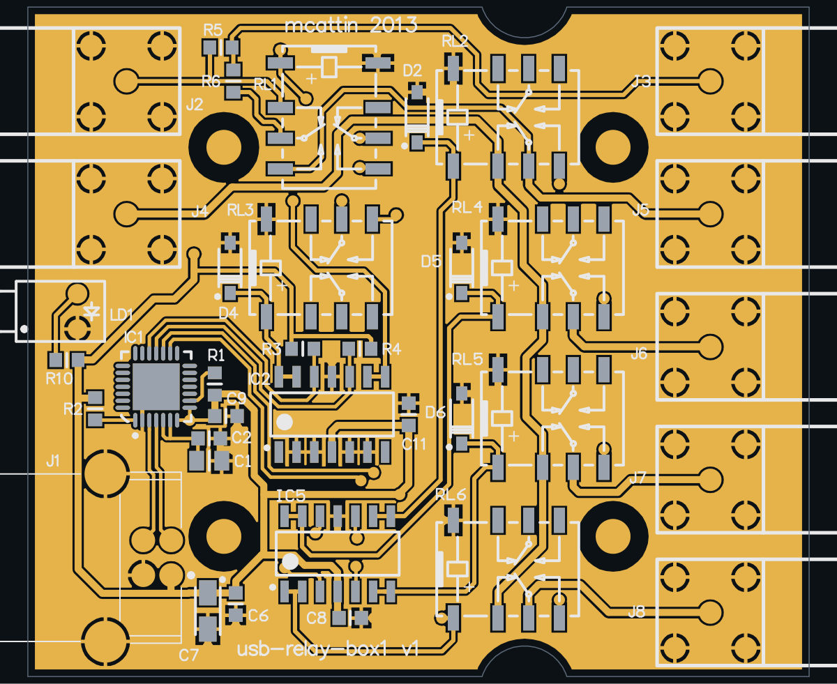
USB RELAY BOX1 (OHWR0025 R1) is an open-hardware circuit board from the CERN Open Hardware Repository, designed in Altium Designer: a 2-layer board of 56 × 48 mm with 52 components and 36 nets, published under GPL-2.0-only.
review 86% walked · 13 findings: 9 major · 4 minor (26 items)
Open in the interactive viewerRead the full review
Design review
Probe recorded 13 findings: 9 major · 4 minor (26 items) on this design. Each is shown here with its reasoning; the full review links every one to the pins, nets and datasheet pages it rests on.
ADR445 5 V reference is powered from USB VBUS, below its 5.5 V minimum input
The ADR445 5.000 V reference IC4 is powered from USB VBUS (+5V), below its 5.5 V minimum input, so VREF cannot be regulated to 5.000 V on this board.
Where it is
``
mermaid flowchart LR J1["J1 pin 1<br/>USB VBUS"] -- "+5V" --> IC4["IC4 ADR445BRZ<br/>VIN pin 2"] IC4 -- "VOUT pin 6" --> VREF["VREF"]``No other supply source is on the board.
The numbers
Quantity Value Source ADR445 supply operating range 5.5 V to 18 V ADR445 datasheet, p.7 Supply on this board +5V = USB VBUS netlist: J1 pin 1, IC4 pin 2 LMV324 op-amp outputs cannot guarantee the 21 mA the G6K relay coils need
The G6K relay coils RL1-RL6 are driven directly from LMV324 op-amp outputs (IC2C, IC2D, IC5A-IC5D), which guarantee only 5 mA of source current where each coil needs 21 mA.
Where it is
Each coil is driven from an op-amp output with the coil return to GND, e.g. RL3 pin 1 (NetD4_1) from IC2 pin 14 (IC2D output), RL3 pin 8 on GND.
Relay Driver RL1 IC2C RL3 IC2D RL2, RL4, RL5, RL6 IC5A-IC5D The numbers
Quantity Value Source G6K-2F-Y-5VDC coil current 21.1 mA at 5 V (237 ohm coil) G6K datasheet, p.3 Must-operate voltage 80% of rated G6K datasheet, p.3 LMV324 guaranteed output short-circuit sourcing current 5 mA min at 25 C LMV324 datasheet, p.7 Relay coils exceed the USB bus-power budget, with three relays always energised even in suspend
The relay coils exceed the USB bus-power budget: the 74HCT139 half IC3B has its enable 2E grounded, so three of RL2/RL4/RL5/RL6 are energised whenever VBUS is present, even in suspend.
Why three coils are always on
- IC3B's enable 2E (IC3 pin 15) is tied to GND, so exactly one of its active-LOW outputs 2Y0 to 2Y3 (pins 12, 11, 10, 9) is low and the other three are high at all times (74HCT139 datasheet, p.1).
- Through IC5, those three high outputs energise three of RL2, RL4, RL5, RL6 whenever VBUS is present.
- RL1 and RL3 add 21 mA each when GPIO0 and GPIO1 are high.
The numbers
Quantity Value Source G6K-2F-Y-5VDC coil current 21.1 mA at 5 V G6K datasheet, p.3 Three standing coils about 63 mA derived CP2103 supply current 20 mA typ, 26 mA max CP2103 datasheet, p.5 Standing total: three coils, CP2103, ADR445 (3 mA) and the op-amps about 90 mA derived With RL1 and RL3 on as well about 130 mA derived USB 2.0 limit before configuration / low-power function 100 mA USB 2.0 specification, section 7.2.1 USB 2.0 limit in suspend 2.5 mA USB 2.0 specification, section 7.2.1 - ReferencePlaneDiscontinuitymajorOpen
9 nets cross one void in the GND plane on BOTTOM_LAYER and the GND plane on TOP_LAYER at 13 places, the longest 6.19 mm; 16 over tracks of other nets routed inside it (fastest: AWG at 100 ps 10-90 %, ASSUMED)
Along 'AWG' on TOP_LAYER, the GND plane on BOTTOM_LAYER has 6.19 mm under the track with copper of NetC12_1, not a plane, at (30.7, 46.1), the same plane on both sides. No single drill's anti-pad and no landing explains it: a clearance is excused only when it holds a drill and is drawn round it, or the track ends in it on the net's own pad or via, or runs through its own via's clearance and no farther. The return current detours round the void. 16 of the crossings pass over tracks of other nets routed inside the hole on the reference layer: the plane is absent there, and those tracks stand in it. 7 of them run ALONG the bare copper, parallel to its edges, rather than across it (the longest 6.19 mm). 13 places on 9 net(s) cross it, listed below, the longest first. What cleared it: the hole at x 12.59..46.04, y 10.99..48.21 and the hole at x 36.75..51.28, y 9.35..13.21 and the hole at x 39.95..51.28, y 18.99..22.25 and the hole at x 39.95..51.28, y 28.88..33.05 and the hole at x 4.4..51.28, y 7.69..48.57. One decision covers the void: whether these tracks may cross it, or the plane should be filled under them. No crossing has a plane on the track's other side, so the whole return meets the break.
- 'AWG' on TOP_LAYER at (30.7, 46.1), 6.19 mm, running ALONG the bare copper for 6.19 mm, not across it over copper of NetC12_1, not a plane; other side: none: the signal layer is outermost
- one crossing of two tracks, seen from each: 'NetJ5_1' on TOP_LAYER at (37.3, 43.78), 5.72 mm, running ALONG the bare copper for 1.54 mm, not across it over copper of VREF_OUT, +5V, not a plane; other side: none: the signal layer is outermost / 'VREF_OUT' on BOTTOM_LAYER at (35.92, 46.34), 0.87 mm over copper of NetJ5_1, not a plane; other side: none: the signal layer is outermost
- 'NetD1_1' on TOP_LAYER at (21.43, 35.97), 3.25 mm, running ALONG the bare copper for 1.65 mm, not across it over copper of +5V, not a plane; other side: none: the signal layer is outermost
- one crossing of two tracks, seen from each: 'NetJ5_1' on TOP_LAYER at (42.39, 40.51), 0.93 mm over copper of VREF_OUT, not a plane; other side: none: the signal layer is outermost / 'VREF_OUT' on BOTTOM_LAYER at (42.7, 39), 3 mm, running ALONG the bare copper for 1.95 mm, not across it over copper of NetJ5_1, not a plane; other side: none: the signal layer is outermost
- 'AWG' on TOP_LAYER at (35.1, 43.9), 2.55 mm, running ALONG the bare copper for 0.93 mm, not across it over copper of +5V, not a plane; other side: none: the signal layer is outermost
- 'NetD1_1' on TOP_LAYER at (24.3, 35.3), 2.16 mm, running ALONG the bare copper for 1.86 mm, not across it over unnetted copper; other side: none: the signal layer is outermost
- 'NetJ3_1' on TOP_LAYER at (36.1, 47.9), 2.16 mm, running ALONG the bare copper for 2.16 mm, not across it over unnetted copper; other side: none: the signal layer is outermost
- 'NetD2_1' on TOP_LAYER at (31, 34.6), 1.61 mm over copper of +5V, not a plane; other side: none: the signal layer is outermost
- 'NetD1_1' on TOP_LAYER at (27.01, 33.5), 1.26 mm over copper of +5V, not a plane; other side: none: the signal layer is outermost
- one crossing of two tracks, seen from each: 'NetJ7_1' on TOP_LAYER at (41.44, 19.4), 1.16 mm over copper of VREF_OUT, not a plane; other side: none: the signal layer is outermost / 'VREF_OUT' on BOTTOM_LAYER at (41.02, 19.42), 1.05 mm over copper of NetJ7_1, not a plane; other side: none: the signal layer is outermost
- one crossing of two tracks, seen from each: 'AWG' on TOP_LAYER at (33.36, 46.1), 1.07 mm over copper of VREF_OUT, not a plane; other side: none: the signal layer is outermost / 'VREF_OUT' on BOTTOM_LAYER at (33.7, 46), 0.85 mm over copper of AWG, not a plane; other side: none: the signal layer is outermost
- one crossing of two tracks, seen from each: 'NetJ6_1' on TOP_LAYER at (42.39, 29.83), 0.93 mm over copper of VREF_OUT, not a plane; other side: none: the signal layer is outermost / 'VREF_OUT' on BOTTOM_LAYER at (42.7, 29.83), 0.82 mm over copper of NetJ6_1, not a plane; other side: none: the signal layer is outermost
- and 1 more
Every site is a row of this finding's evidence, keyed by net, layers and position. GET /api/odb/boards/3/reference-planes?group=void%3AGND%40BOTTOM_LAYER%3Ahole%2012.59%2C10.99%7C46.04%2C48.21 serves each with its own layer_image region; all of them lie in x 19.4..44.17, y 11.39..48.9 mm (board frame, Y up).
Read from the copper as drawn on the reference layer, along each track's centreline at exact breakpoints. The reference is the copper beside the track, never the layer's type or name. Whether it matters depends on each signal's edge rate, which nothing on file states for these nets: a slow static line crosses a split harmlessly, a fast edge does not.
At void:GND@BOTTOM_LAYER:hole 12.59,10.99|46.04,48.21
- EsdProtectorPlacementmajorOpen
EsdProtectorPlacement: 3 components×3
Checked by the review, stands · Claude walker W4 (Cern session) — Checked (W4, fleet re-walk): the placement is measured from the copper as stated (D3.2 on 'D_N': D3.2 hangs 1.85 mm off the line (limit 1 mm, default; D3.3 on 'D_P': D3.3 hangs 1.75 mm off the line (limit 1 mm, default; D3.4 on '+5V': 1 via(s) between J1.1 and D3.4). Protector placement guidance (on the line, near the connector, no vias/stubs) is layout practice from protector app notes; its effect depends on the ESD event and the protected part's rating, not on file here. Left open for the owner.
At D3
Each finding, with its own headline
D3D3.2 on 'D_N': D3.2 hangs 1.85 mm off the line (limit 1 mm, default
D3 (PRTR5V0U2X) protects 'D_N' at J1.2. Along the copper: 1.85 mm of track from the contact, 0 via(s) before it, on a 1.85 mm branch off the line; the line runs 9.05 mm on to IC1.4; D3 sits at J1, within 0.34 mm of the nearest place outside it to the contact: the track to it is mostly the escape out of J1's own pins, which no placement shortens.
D3.2 hangs 1.85 mm off the line (limit 1 mm, default: no datasheet figure on file): the line carries the strike past it while the clamp is reached through the branch.
Measured on the copper the ODB states: tracks, the pads they land on, and the netlist's vias. Not a straight line between centroids.
D3D3.3 on 'D_P': D3.3 hangs 1.75 mm off the line (limit 1 mm, default
D3 (PRTR5V0U2X) protects 'D_P' at J1.3. Along the copper: 1.75 mm of track from the contact, 0 via(s) before it, on a 1.75 mm branch off the line; the line runs 9.05 mm on to IC1.3; D3 sits at J1, within 0 mm of the nearest place outside it to the contact: the track to it is mostly the escape out of J1's own pins, which no placement shortens.
D3.3 hangs 1.75 mm off the line (limit 1 mm, default: no datasheet figure on file): the line carries the strike past it while the clamp is reached through the branch.
Measured on the copper the ODB states: tracks, the pads they land on, and the netlist's vias. Not a straight line between centroids.
D3D3.4 on '+5V': 1 via(s) between J1.1 and D3.4
D3 (PRTR5V0U2X) protects '+5V' at J1.1. Along the copper: 33 mm of track from the contact, 1 via(s) before it, on a 29.18 mm branch off the line; the line runs 3.82 mm on to C7.1; D3 sits 2.84 mm farther from the contact than the nearest place outside J1.
1 via(s) between J1.1 and D3.4: the strike reaches an inner layer before it is clamped. D3.4 hangs 29.18 mm off the line (limit 1 mm, default: no datasheet figure on file): the line carries the strike past it while the clamp is reached through the branch.
Measured on the copper the ODB states: tracks, the pads they land on, and the netlist's vias. Not a straight line between centroids.
- FiducialMissingmajorOpen
FiducialMissing: 2 boards×2
2 checked by the review by Claude walker (cern session) — 2 different reasons
At bottom, top
Each finding, with its own headline
bottomThe bottom side carries 16 SMT component(s) and no fiducial was found on it
The bottom side carries 16 SMT component(s) but no fiducial was found on it — a placement machine has no optical reference to align to. Probe found no pad labelled .pad_usage=g_fiducial/l_fiducial (basis pad_usage); no single-pad, netless, undrilled component whose 0.5-3 mm round pad has a concentric solder-mask opening at least 1.5x its diameter with no other copper inside it (basis geometry); and no component whose refdes starts FID or whose part or package name contains FIDUCIAL (basis footprint-name). If your library names fiducials something Probe does not recognise, mark this benign — disposition_finding(rule='FiducialMissing', entity='bottom', status='benign', reason=…) — the name match only ever silences this check, it never asserts anything. If the side really has no fiducial, say so with status='confirmed': that answers the finding and keeps it gating release.
topThe top side carries 27 SMT component(s) and no fiducial was found on it
The top side carries 27 SMT component(s) but no fiducial was found on it — a placement machine has no optical reference to align to. Probe found no pad labelled .pad_usage=g_fiducial/l_fiducial (basis pad_usage); no single-pad, netless, undrilled component whose 0.5-3 mm round pad has a concentric solder-mask opening at least 1.5x its diameter with no other copper inside it (basis geometry); and no component whose refdes starts FID or whose part or package name contains FIDUCIAL (basis footprint-name). If your library names fiducials something Probe does not recognise, mark this benign — disposition_finding(rule='FiducialMissing', entity='top', status='benign', reason=…) — the name match only ever silences this check, it never asserts anything. If the side really has no fiducial, say so with status='confirmed': that answers the finding and keeps it gating release.
- SinglePointNetmajorOpen
IC1.24 (RXD) is an IC input left unconnected
Pin IC1.24 (RXD) is an IC INPUT left UNCONNECTED (on the no-connect bucket). Marked no-connect by the designer, but an input normally needs a defined level - confirm it is truly meant to float. If the datasheet defines this input left open (an internal pull, "read as low when left floating", or a tri-level input whose open state is one of its settings), file it on the pin as if_unused (pull_up, pull_down or may_float) with submit_pin_behavior, citing the page, and this finding clears.
At IC1.24
- PartLifecyclemajorOpen
LMV324ID on 2 placements (IC2, IC5): the distributor catalogue reports "Obsolete" for Texas Instruments's LMV324ID
LMV324ID on 2 placements (IC2, IC5): the distributor catalogue reports "Obsolete" for Texas Instruments's LMV324ID — a sourcing/longevity risk to confirm against the MANUFACTURER before acting. This board's BOM names no manufacturer for it, so whether that is the fitted maker's product was not checked. A distributor delisting is not the same claim as the part being unavailable; check the vendor's own lifecycle/product-change notice for the status and any named successor. Re-read the source: GET /api/odb/parts/LMV324ID/providers (which provider said it, the maker and part number it matched, its own words, and when we asked). THE LAST BUY DATE HAS PASSED (2024-02-23, 996 day(s) ago), so this is a substitution rather than a buy. The distributor reports NONE left. No approved alternate is recorded for this position.
At IC2
- ReferencePlaneDiscontinuitymajorOpen
ReferencePlaneDiscontinuity: 11 boards×11
11 checked by the review by Claude walker W4 (Cern session) — 11 different reasons
At void:GND@BOTTOM_LAYER:hole 18.56,11.22|26.9,21.54, void:GND@BOTTOM_LAYER:hole 19.69,39.59|22.05,48.34, void:GND@BOTTOM_LAYER:hole 26.91,11.22|30.51,19.97, void:GND@BOTTOM_LAYER:hole 30.35,9.68|32.33,12.98, void:GND@BOTTOM_LAYER:hole 37.09,41.52|37.72,42.13, void:GND@BOTTOM_LAYER:hole 8.84,19|13.71,25.29 and 5 more
Each finding, with its own headline
void:GND@BOTTOM_LAYER:hole 18.56,11.22|26.9,21.544 nets cross one void in the GND plane on BOTTOM_LAYER and the GND plane on TOP_LAYER at 3 places, the longest 5.21 mm; 3 over tracks of other nets routed inside it (fastest: NetD2_1 at 100 ps 10-90 %, ASSUMED)
Along 'NetD5_1' on TOP_LAYER, the GND plane on BOTTOM_LAYER has 5.21 mm under the track with copper of NetIC3_10, not a plane, at (21.07, 16.81), running to the end of the track. No single drill's anti-pad and no landing explains it: a clearance is excused only when it holds a drill and is drawn round it, or the track ends in it on the net's own pad or via, or runs through its own via's clearance and no farther. The return current detours round the void. 3 of the crossings pass over tracks of other nets routed inside the hole on the reference layer: the plane is absent there, and those tracks stand in it. 3 of them run ALONG the bare copper, parallel to its edges, rather than across it (the longest 3.15 mm). 3 places on 4 net(s) cross it, listed below, the longest first. What cleared it: the hole at x 18.56..26.9, y 11.22..21.54 and the hole at x 4.4..51.28, y 7.69..48.57. One decision covers the void: whether these tracks may cross it, or the plane should be filled under them. No crossing has a plane on the track's other side, so the whole return meets the break.
- one crossing of two tracks, seen from each: 'NetD5_1' on TOP_LAYER at (21.07, 16.81), 5.21 mm, running ALONG the bare copper for 3.15 mm, not across it over copper of NetIC3_10, not a plane, to the end of the track; other side: none: the signal layer is outermost / 'NetIC3_10' on BOTTOM_LAYER at (20.43, 17.47), 0.31 mm over copper of NetD5_1, not a plane, to the end of the track; other side: none: the signal layer is outermost / 'NetIC3_10' on BOTTOM_LAYER at (21.5, 15.31), 3.84 mm, running ALONG the bare copper for 0.66 mm, not across it over copper of NetD5_1, +5V, not a plane; other side: none: the signal layer is outermost
- 'NetD7_1' on TOP_LAYER at (20.56, 11.91), 2.35 mm, running ALONG the bare copper for 1.87 mm, not across it over unnetted copper, to the end of the track; other side: none: the signal layer is outermost
- 'NetD2_1' on TOP_LAYER at (26.32, 17.7), 0.51 mm over copper of GND, not a plane, to the end of the track; other side: none: the signal layer is outermost
Every site is a row of this finding's evidence, keyed by net, layers and position. GET /api/odb/boards/3/reference-planes?group=void%3AGND%40BOTTOM_LAYER%3Ahole%2018.56%2C11.22%7C26.9%2C21.54 serves each with its own layer_image region; all of them lie in x 18.8..27.66, y 10.22..18.7 mm (board frame, Y up).
Read from the copper as drawn on the reference layer, along each track's centreline at exact breakpoints. The reference is the copper beside the track, never the layer's type or name. Whether it matters depends on each signal's edge rate, which nothing on file states for these nets: a slow static line crosses a split harmlessly, a fast edge does not.
void:GND@BOTTOM_LAYER:hole 19.69,39.59|22.05,48.343 nets cross one void in the GND plane on BOTTOM_LAYER and the GND plane on TOP_LAYER at 2 places, the longest 1.03 mm; 4 over tracks of other nets routed inside it (fastest: AWG at 100 ps 10-90 %, ASSUMED)
Along 'AWG' on TOP_LAYER, the GND plane on BOTTOM_LAYER has 1.03 mm under the track with copper of NetD1_1, not a plane, at (20.94, 41.3), the same plane on both sides. No single drill's anti-pad and no landing explains it: a clearance is excused only when it holds a drill and is drawn round it, or the track ends in it on the net's own pad or via, or runs through its own via's clearance and no farther. The return current detours round the void. 4 of the crossings pass over tracks of other nets routed inside the hole on the reference layer: the plane is absent there, and those tracks stand in it. 2 places on 3 net(s) cross it, listed below, the longest first. What cleared it: the hole at x 19.69..22.05, y 39.59..48.34 and the hole at x 4.4..51.28, y 7.69..48.57. One decision covers the void: whether these tracks may cross it, or the plane should be filled under them. No crossing has a plane on the track's other side, so the whole return meets the break.
- one crossing of two tracks, seen from each: 'AWG' on TOP_LAYER at (20.94, 41.3), 1.03 mm over copper of NetD1_1, not a plane; other side: none: the signal layer is outermost / 'NetD1_1' on BOTTOM_LAYER at (21.3, 41.38), 0.95 mm over copper of AWG, not a plane; other side: none: the signal layer is outermost
- one crossing of two tracks, seen from each: 'NetD1_1' on BOTTOM_LAYER at (21.3, 42.6), 0.62 mm over copper of NetJ5_1, not a plane; other side: none: the signal layer is outermost / 'NetJ5_1' on TOP_LAYER at (20.99, 42.6), 0.98 mm over copper of NetD1_1, not a plane; other side: none: the signal layer is outermost
Every site is a row of this finding's evidence, keyed by net, layers and position. GET /api/odb/boards/3/reference-planes?group=void%3AGND%40BOTTOM_LAYER%3Ahole%2019.69%2C39.59%7C22.05%2C48.34 serves each with its own layer_image region; all of them lie in x 19.74..22.77, y 39.89..43.91 mm (board frame, Y up).
Read from the copper as drawn on the reference layer, along each track's centreline at exact breakpoints. The reference is the copper beside the track, never the layer's type or name. Whether it matters depends on each signal's edge rate, which nothing on file states for these nets: a slow static line crosses a split harmlessly, a fast edge does not.
void:GND@BOTTOM_LAYER:hole 26.91,11.22|30.51,19.973 nets cross one void in the GND plane on BOTTOM_LAYER at 5 places, the longest 2.3 mm; 3 over tracks of other nets routed inside it (fastest: NetD2_1 at 100 ps 10-90 %, ASSUMED)
Along 'NetD2_1' on TOP_LAYER, the GND plane on BOTTOM_LAYER has 2.3 mm under the track with copper of GND, +5V, not a plane, at (28.05, 17.7), the same plane on both sides. No single drill's anti-pad and no landing explains it: a clearance is excused only when it holds a drill and is drawn round it, or the track ends in it on the net's own pad or via, or runs through its own via's clearance and no farther. The return current detours round the void. 3 of the crossings pass over tracks of other nets routed inside the hole on the reference layer: the plane is absent there, and those tracks stand in it. 1 of them run ALONG the bare copper, parallel to its edges, rather than across it (the longest 0.54 mm). 5 places on 3 net(s) cross it, listed below, the longest first. What cleared it: the hole at x 26.91..30.51, y 11.22..19.97. One decision covers the void: whether these tracks may cross it, or the plane should be filled under them. No crossing has a plane on the track's other side, so the whole return meets the break.
- 'NetD2_1' on TOP_LAYER at (28.05, 17.7), 2.3 mm, running ALONG the bare copper for 0.54 mm, not across it over copper of GND, +5V, not a plane; other side: none: the signal layer is outermost
- 'NetD6_1' on TOP_LAYER at (27.42, 12.3), 1.75 mm over copper of GND, +5V, not a plane, to the end of the track; other side: none: the signal layer is outermost
- 'NetD5_1' on TOP_LAYER at (28.05, 16.45), 1.66 mm over copper of +5V, not a plane; other side: none: the signal layer is outermost
- 'NetD5_1' on TOP_LAYER at (29.35, 17.75), 1.44 mm over copper of +5V, not a plane; other side: none: the signal layer is outermost
- 'NetD6_1' on TOP_LAYER at (27.25, 12.3), 0.51 mm over copper of GND, not a plane, to the end of the track; other side: none: the signal layer is outermost
Every site is a row of this finding's evidence, keyed by net, layers and position. GET /api/odb/boards/3/reference-planes?group=void%3AGND%40BOTTOM_LAYER%3Ahole%2026.91%2C11.22%7C30.51%2C19.97 serves each with its own layer_image region; all of them lie in x 25.91..30.75, y 11.3..19.27 mm (board frame, Y up).
Read from the copper as drawn on the reference layer, along each track's centreline at exact breakpoints. The reference is the copper beside the track, never the layer's type or name. Whether it matters depends on each signal's edge rate, which nothing on file states for these nets: a slow static line crosses a split harmlessly, a fast edge does not.
void:GND@BOTTOM_LAYER:hole 30.35,9.68|32.33,12.98'NetD6_1' crosses one void in the GND plane on BOTTOM_LAYER at 1 place, the longest 1.41 mm (fastest: NetD6_1 at 100 ps 10-90 %, ASSUMED)
Along 'NetD6_1' on TOP_LAYER, the GND plane on BOTTOM_LAYER has 1.41 mm under the track with copper of NetD7_1, not a plane, at (31.62, 12.3), the same plane on both sides. No single drill's anti-pad and no landing explains it: a clearance is excused only when it holds a drill and is drawn round it, or the track ends in it on the net's own pad or via, or runs through its own via's clearance and no farther. The return current detours round the void. 1 of them run ALONG the bare copper, parallel to its edges, rather than across it (the longest 1.41 mm). What cleared it: the hole at x 30.35..32.33, y 9.68..12.98. One decision covers the void: whether these tracks may cross it, or the plane should be filled under them. No crossing has a plane on the track's other side, so the whole return meets the break.
- 'NetD6_1' on TOP_LAYER at (31.62, 12.3), 1.41 mm, running ALONG the bare copper for 1.41 mm, not across it over copper of NetD7_1, not a plane; other side: none: the signal layer is outermost
Every site is a row of this finding's evidence, keyed by net, layers and position. GET /api/odb/boards/3/reference-planes?group=void%3AGND%40BOTTOM_LAYER%3Ahole%2030.35%2C9.68%7C32.33%2C12.98 serves each with its own layer_image region; all of them lie in x 29.92..33.33, y 11.3..13.3 mm (board frame, Y up).
Read from the copper as drawn on the reference layer, along each track's centreline at exact breakpoints. The reference is the copper beside the track, never the layer's type or name. Whether it matters depends on each signal's edge rate, which nothing on file states for these nets: a slow static line crosses a split harmlessly, a fast edge does not.
void:GND@BOTTOM_LAYER:hole 37.09,41.52|37.72,42.13'NetJ5_1' crosses one void in the GND plane on BOTTOM_LAYER at 1 place, the longest 0.6 mm (fastest: NetJ5_1 at 100 ps 10-90 %, ASSUMED)
Along 'NetJ5_1' on TOP_LAYER, the GND plane on BOTTOM_LAYER has 0.6 mm under the track with no copper, at (37.3, 41.83), the same plane on both sides. No single drill's anti-pad and no landing explains it: a clearance is excused only when it holds a drill and is drawn round it, or the track ends in it on the net's own pad or via, or runs through its own via's clearance and no farther. The return current detours round the void. 1 of them run ALONG the bare copper, parallel to its edges, rather than across it (the longest 0.6 mm). What cleared it: the hole at x 37.09..37.72, y 41.52..42.13. One decision covers the void: whether these tracks may cross it, or the plane should be filled under them. No crossing has a plane on the track's other side, so the whole return meets the break.
- 'NetJ5_1' on TOP_LAYER at (37.3, 41.83), 0.6 mm, running ALONG the bare copper for 0.6 mm, not across it over no copper; other side: none: the signal layer is outermost
Every site is a row of this finding's evidence, keyed by net, layers and position. GET /api/odb/boards/3/reference-planes?group=void%3AGND%40BOTTOM_LAYER%3Ahole%2037.09%2C41.52%7C37.72%2C42.13 serves each with its own layer_image region; all of them lie in x 36.3..38.3, y 40.52..43.13 mm (board frame, Y up).
Read from the copper as drawn on the reference layer, along each track's centreline at exact breakpoints. The reference is the copper beside the track, never the layer's type or name. Whether it matters depends on each signal's edge rate, which nothing on file states for these nets: a slow static line crosses a split harmlessly, a fast edge does not.
void:GND@BOTTOM_LAYER:hole 8.84,19|13.71,25.292 nets cross one void in the GND plane on BOTTOM_LAYER at 3 places, the longest 1.66 mm; 2 over tracks of other nets routed inside it (fastest: D_N at 100 ps 10-90 %, ASSUMED)
Along 'D_P' on TOP_LAYER, the GND plane on BOTTOM_LAYER has 1.66 mm under the track with copper of +5V, not a plane, at (10.1, 21.68), the same plane on both sides. No single drill's anti-pad and no landing explains it: a clearance is excused only when it holds a drill and is drawn round it, or the track ends in it on the net's own pad or via, or runs through its own via's clearance and no farther. The return current detours round the void. 2 of the crossings pass over tracks of other nets routed inside the hole on the reference layer: the plane is absent there, and those tracks stand in it. 1 of them run ALONG the bare copper, parallel to its edges, rather than across it (the longest 1.21 mm). 3 places on 2 net(s) cross it, listed below, the longest first. What cleared it: the hole at x 8.84..13.71, y 19..25.29. One decision covers the void: whether these tracks may cross it, or the plane should be filled under them. No crossing has a plane on the track's other side, so the whole return meets the break.
- 'D_P' on TOP_LAYER at (10.1, 21.68), 1.66 mm over copper of +5V, not a plane; other side: none: the signal layer is outermost
- 'D_N' on TOP_LAYER at (10.61, 22.19), 1.61 mm over copper of +5V, not a plane; other side: none: the signal layer is outermost
- 'D_P' on TOP_LAYER at (10.42, 19.61), 1.21 mm, running ALONG the bare copper for 1.21 mm, not across it over no copper; other side: none: the signal layer is outermost
Every site is a row of this finding's evidence, keyed by net, layers and position. GET /api/odb/boards/3/reference-planes?group=void%3AGND%40BOTTOM_LAYER%3Ahole%208.84%2C19%7C13.71%2C25.29 serves each with its own layer_image region; all of them lie in x 9.1..11.61, y 18..23.99 mm (board frame, Y up).
Read from the copper as drawn on the reference layer, along each track's centreline at exact breakpoints. The reference is the copper beside the track, never the layer's type or name. Whether it matters depends on each signal's edge rate, which nothing on file states for these nets: a slow static line crosses a split harmlessly, a fast edge does not.
void:GND@TOP_LAYER:hole 38.95,16.35|40.05,18.45'VREF_OUT' crosses one void in the GND plane on TOP_LAYER at 1 place, the longest 2.33 mm (fastest: VREF_OUT at 100 ps 10-90 %, ASSUMED)
Along 'VREF_OUT' on BOTTOM_LAYER, the GND plane on TOP_LAYER has 2.33 mm under the track with unnetted copper, at (39.5, 17.2), the same plane on both sides. No single drill's anti-pad and no landing explains it: a clearance is excused only when it holds a drill and is drawn round it, or the track ends in it on the net's own pad or via, or runs through its own via's clearance and no farther. The return current detours round the void. 1 of them run ALONG the bare copper, parallel to its edges, rather than across it (the longest 1.55 mm). What cleared it: the hole at x 38.95..40.05, y 16.35..18.45. One decision covers the void: whether these tracks may cross it, or the plane should be filled under them. No crossing has a plane on the track's other side, so the whole return meets the break.
- 'VREF_OUT' on BOTTOM_LAYER at (39.5, 17.2), 2.33 mm, running ALONG the bare copper for 1.55 mm, not across it over unnetted copper; other side: none: the signal layer is outermost
Every site is a row of this finding's evidence, keyed by net, layers and position. GET /api/odb/boards/3/reference-planes?group=void%3AGND%40TOP_LAYER%3Ahole%2038.95%2C16.35%7C40.05%2C18.45 serves each with its own layer_image region; all of them lie in x 38.5..41.05, y 15.35..19.45 mm (board frame, Y up).
Read from the copper as drawn on the reference layer, along each track's centreline at exact breakpoints. The reference is the copper beside the track, never the layer's type or name. Whether it matters depends on each signal's edge rate, which nothing on file states for these nets: a slow static line crosses a split harmlessly, a fast edge does not.
void:GND@TOP_LAYER:hole 4.4,7.69|51.28,48.575 nets cross one void in the GND plane on TOP_LAYER at 5 places, the longest 4.73 mm; 5 over tracks of other nets routed inside it (fastest: NetC12_1 at 100 ps 10-90 %, ASSUMED)
Along 'NetC12_1' on BOTTOM_LAYER, the GND plane on TOP_LAYER has 4.73 mm under the track with copper of AWG, not a plane, at (27.65, 46.3), running to the end of the track. No single drill's anti-pad and no landing explains it: a clearance is excused only when it holds a drill and is drawn round it, or the track ends in it on the net's own pad or via, or runs through its own via's clearance and no farther. The return current detours round the void. 5 of the crossings pass over tracks of other nets routed inside the hole on the reference layer: the plane is absent there, and those tracks stand in it. 1 of them run ALONG the bare copper, parallel to its edges, rather than across it (the longest 4.07 mm). 5 places on 5 net(s) cross it, listed below, the longest first. What cleared it: the hole at x 4.4..51.28, y 7.69..48.57. One decision covers the void: whether these tracks may cross it, or the plane should be filled under them. No crossing has a plane on the track's other side, so the whole return meets the break.
- 'NetC12_1' on BOTTOM_LAYER at (27.65, 46.3), 4.73 mm, running ALONG the bare copper for 4.07 mm, not across it over copper of AWG, not a plane, to the end of the track; other side: none: the signal layer is outermost
- 'GPIO3' on BOTTOM_LAYER at (24.76, 19.74), 1.43 mm over copper of +5V, not a plane, to the end of the track; other side: none: the signal layer is outermost
- 'GPIO2' on BOTTOM_LAYER at (25.51, 19.23), 0.91 mm over copper of +5V, not a plane; other side: none: the signal layer is outermost
- 'NetIC3_9' on BOTTOM_LAYER at (19.81, 14.9), 0.91 mm over copper of +5V, not a plane, to the end of the track; other side: none: the signal layer is outermost
- 'NetD7_1' on BOTTOM_LAYER at (31.62, 12.07), 0.18 mm over copper of NetD6_1, not a plane, to the end of the track; other side: none: the signal layer is outermost
Every site is a row of this finding's evidence, keyed by net, layers and position. GET /api/odb/boards/3/reference-planes?group=void%3AGND%40TOP_LAYER%3Ahole%204.4%2C7.69%7C51.28%2C48.57 serves each with its own layer_image region; all of them lie in x 18.81..32.62, y 10.99..47.34 mm (board frame, Y up).
Read from the copper as drawn on the reference layer, along each track's centreline at exact breakpoints. The reference is the copper beside the track, never the layer's type or name. Whether it matters depends on each signal's edge rate, which nothing on file states for these nets: a slow static line crosses a split harmlessly, a fast edge does not.
void:GND@TOP_LAYER:hole 42.14,20.15|43.26,23.06'VREF_OUT' crosses one void in the GND plane on TOP_LAYER at 1 place, the longest 0.37 mm (fastest: VREF_OUT at 100 ps 10-90 %, ASSUMED)
Along 'VREF_OUT' on BOTTOM_LAYER, the GND plane on TOP_LAYER has 0.37 mm under the track with no copper, at (42.23, 20.63), the same plane on both sides. No single drill's anti-pad and no landing explains it: a clearance is excused only when it holds a drill and is drawn round it, or the track ends in it on the net's own pad or via, or runs through its own via's clearance and no farther. The return current detours round the void. What cleared it: the hole at x 42.14..43.26, y 20.15..23.06. One decision covers the void: whether these tracks may cross it, or the plane should be filled under them. No crossing has a plane on the track's other side, so the whole return meets the break.
- 'VREF_OUT' on BOTTOM_LAYER at (42.23, 20.63), 0.37 mm over no copper; other side: none: the signal layer is outermost
Every site is a row of this finding's evidence, keyed by net, layers and position. GET /api/odb/boards/3/reference-planes?group=void%3AGND%40TOP_LAYER%3Ahole%2042.14%2C20.15%7C43.26%2C23.06 serves each with its own layer_image region; all of them lie in x 41.15..43.7, y 19.55..24.06 mm (board frame, Y up).
Read from the copper as drawn on the reference layer, along each track's centreline at exact breakpoints. The reference is the copper beside the track, never the layer's type or name. Whether it matters depends on each signal's edge rate, which nothing on file states for these nets: a slow static line crosses a split harmlessly, a fast edge does not.
void:GND@TOP_LAYER:hole 42.14,30.95|43.26,33.86'VREF_OUT' crosses one void in the GND plane on TOP_LAYER at 1 place, the longest 0.31 mm (fastest: VREF_OUT at 100 ps 10-90 %, ASSUMED)
Along 'VREF_OUT' on BOTTOM_LAYER, the GND plane on TOP_LAYER has 0.31 mm under the track with no copper, at (42.7, 33.78), the same plane on both sides. No single drill's anti-pad and no landing explains it: a clearance is excused only when it holds a drill and is drawn round it, or the track ends in it on the net's own pad or via, or runs through its own via's clearance and no farther. The return current detours round the void. What cleared it: the hole at x 42.14..43.26, y 30.95..33.86. One decision covers the void: whether these tracks may cross it, or the plane should be filled under them. No crossing has a plane on the track's other side, so the whole return meets the break.
- 'VREF_OUT' on BOTTOM_LAYER at (42.7, 33.78), 0.31 mm over no copper; other side: none: the signal layer is outermost
Every site is a row of this finding's evidence, keyed by net, layers and position. GET /api/odb/boards/3/reference-planes?group=void%3AGND%40TOP_LAYER%3Ahole%2042.14%2C30.95%7C43.26%2C33.86 serves each with its own layer_image region; all of them lie in x 41.7..43.7, y 29.95..34.86 mm (board frame, Y up).
Read from the copper as drawn on the reference layer, along each track's centreline at exact breakpoints. The reference is the copper beside the track, never the layer's type or name. Whether it matters depends on each signal's edge rate, which nothing on file states for these nets: a slow static line crosses a split harmlessly, a fast edge does not.
void:GND@TOP_LAYER:hole 42.15,27.15|43.25,29.25'VREF_OUT' crosses one void in the GND plane on TOP_LAYER at 1 place, the longest 2.1 mm (fastest: VREF_OUT at 100 ps 10-90 %, ASSUMED)
Along 'VREF_OUT' on BOTTOM_LAYER, the GND plane on TOP_LAYER has 2.1 mm under the track with unnetted copper, at (42.7, 28.2), the same plane on both sides. No single drill's anti-pad and no landing explains it: a clearance is excused only when it holds a drill and is drawn round it, or the track ends in it on the net's own pad or via, or runs through its own via's clearance and no farther. The return current detours round the void. 1 of them run ALONG the bare copper, parallel to its edges, rather than across it (the longest 2.1 mm). What cleared it: the hole at x 42.15..43.25, y 27.15..29.25. One decision covers the void: whether these tracks may cross it, or the plane should be filled under them. No crossing has a plane on the track's other side, so the whole return meets the break.
- 'VREF_OUT' on BOTTOM_LAYER at (42.7, 28.2), 2.1 mm, running ALONG the bare copper for 2.1 mm, not across it over unnetted copper; other side: none: the signal layer is outermost
Every site is a row of this finding's evidence, keyed by net, layers and position. GET /api/odb/boards/3/reference-planes?group=void%3AGND%40TOP_LAYER%3Ahole%2042.15%2C27.15%7C43.25%2C29.25 serves each with its own layer_image region; all of them lie in x 41.7..43.7, y 26.15..30.25 mm (board frame, Y up).
Read from the copper as drawn on the reference layer, along each track's centreline at exact breakpoints. The reference is the copper beside the track, never the layer's type or name. Whether it matters depends on each signal's edge rate, which nothing on file states for these nets: a slow static line crosses a split harmlessly, a fast edge does not.
Assembly-variant note does not match the BOM and names a resistor that does not exist
The assembly-variant note does not match the BOM: the BOM fits R5, R6 and R7 together, which builds neither documented variant, and the note names an R13 that does not exist.
The note against the BOM
Source R5 R6 R7 Optional parts Note, fmc-adc version fitted not mounted fitted R9, R11, R13 Note, fmc-fd and fmc-tdc version not mounted fitted not mounted R9, R11, R13 Released BOM fitted fitted fitted - The design has no R13: the divider is R9, R11, R12.
Title block has a placeholder document number and checker, and its revision differs from the silkscreen
The schematic title block has a placeholder document number (EDA-XXXXX-VX-X) and checker ("*"), and its revision v3 differs from the silkscreen's v1.
Where What it says Title block, the only schematic sheet Document USB controlled relay box, EDA-XXXXX-VX-X, Check.by "*", Rev v3 PCB silkscreen (top overlay) usb-relay-box1 v1 Calibration voltages produced by the VREF divider and relays are not stated anywhere
The calibration voltages produced on VREF_OUT by the R9/R11/R12 divider and relays RL1/RL3 are not stated anywhere on the schematic.
Where it is
``
mermaid flowchart LR VREF["VREF"] --> R9["R9 270k<br/>shorted by RL3"] R9 --> R11["R11 27k<br/>shorted by RL1"] R11 --> N["NetC12_1"] N --> R12["R12 3k to GND"] N --> IC6["IC6 buffer pin 3"] IC6 --> OUT["VREF_OUT"]``The schematic gives no note of the resulting output levels.
No fiducials on either side of the board
No fiducials on either side of the board, although it carries the 0.5 mm pitch QFN IC1 (CP2103) and parts on both sides.
Neither the top nor the bottom copper, paste or overlay shows a fiducial mark. IC1's footprint is QFN50P500X500X100-29N (0.5 mm pitch).
Main parts
| Part number | Maker | Description | Where |
|---|---|---|---|
| 292304-1 | 4 Pin + 1 Shield USB Receptacle | J1 | |
| 551-1307F | LED Green 1C 2A | LD1 | |
| 74HCT139D | Dual 2-to-4 line decoder/demultiplexer | IC3 | |
| AD8628ARZ | Operational Amplifier | IC6 | |
| ADR445BRZ | 5V Ultralow Noise, LDO XFET Voltage References with Current Sink and Source | IC4 | |
| CP2103 | USB to UART bridge (Silicon Labs CP2103) | IC1 | |
| PRTR5V0U2X | Ultra Low Capacitance Double Rail-to-Rail ESD Protection Diode | D3 | |
| LMV324ID | Quad Operational Amplifier | IC2, IC5 | |
| G6K-2F-Y-5VDC | DPDT Subminiature Relay, G6K-2 Serie | RL1, RL2, RL3, RL4, RL5, RL6 | |
| MBR0540T1G | Schottky Diode | D1, D2, D4, D5, D6, D7 | |
| EPL.00.250.NTN | J2, J3, J4, J5, J6, J7, J8 |
About this design
- Design
- USB RELAY BOX1 — OHWR0025 R1
- Designed in
- Altium Designer
- Board
- 2 copper layers, 56 × 48 mm, 52 components, 36 nets
- Licence
- GPL-2.0-only
- Source
- https://gitlab.com/ohwr/project/usb-relay-box1 at commit
5f3e3ae41096 - Attribution
- CERN Open Hardware Repository, project usb-relay-box1 (path pcb/), commit 5f3e3ae4109660423426967d994eedf31174bf44 (2025-04-09). Licence: GPL-2.0-only (stated repository-wide in .ohwr.yaml). Source: https://gitlab.com/ohwr/project/usb-relay-box1. This is a snapshot of the copy published on the OHWR GitLab pages (R1), not CERN's released record. CERN's source of truth is EDMS (https://edms.cern.ch), and the current release may be newer.
- Reviewed with
- Probe by E# (E-Sharp AB)