 Probe

UTCA RTM 8 SFP
OHWR0029 · revision R1
UTCA RTM 8 SFP (OHWR0029 R1) is an open-hardware circuit board from the CERN Open Hardware Repository, designed in Altium Designer: a 4-layer board of 182.5 × 148.5 mm with 363 components and 312 nets, published under CERN-OHL-1.1.
review 91% walked · 13 findings: 5 major · 8 minor (67 items)
Open in the interactive viewerRead the full review
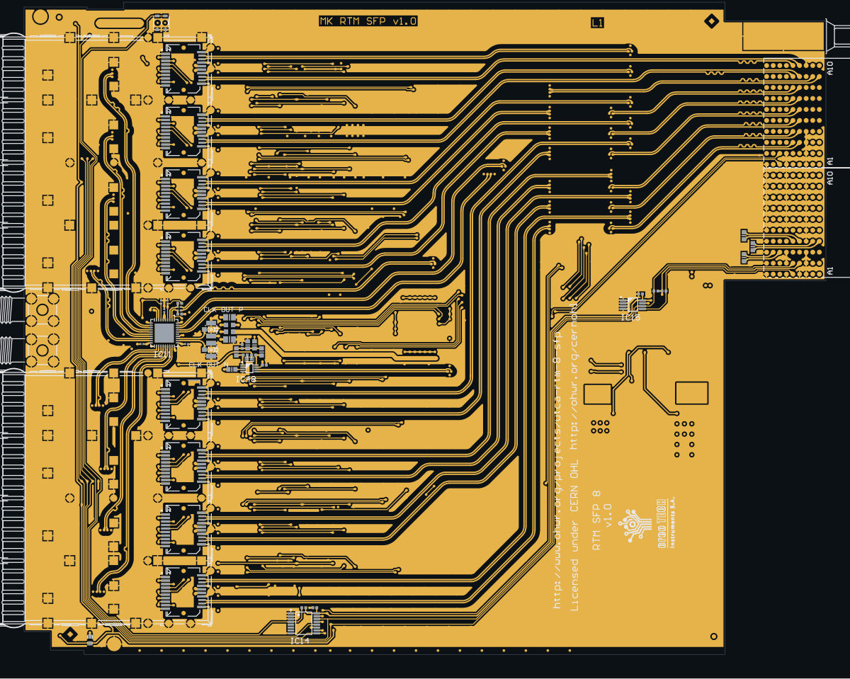
Design review
Probe recorded 13 findings: 5 major · 8 minor (67 items) on this design. Each is shown here with its reasoning; the full review links every one to the pins, nets and datasheet pages it rests on.
100 R pull-downs R2/R3/R4/R5/R13 on the serial-register control lines RTM_IO2..RTM_IO6 need about 23 mA per line from the host to reach a 74HC04 logic high
The 100 R pull-downs R2, R3, R4, R5 and R13 on the serial-register control lines RTM_IO2..RTM_IO6 need about 23 mA per line from the off-board host to reach a 74HC04 (IC1) logic high, about 115 mA for the five lines.
The lines
Each host-driven line goes straight to a 74HC04 input with a 100 R (R0603_100R_1%) resistor to GND, and nothing else on the net.
Net Schematic name (sheet 6) Connector pin IC1 input Pull-down RTM_IO2 REG_OEn J6.C7 pin 11 R5 RTM_IO3 REG_CLKn J6.C8 pin 3 R13 RTM_IO4 REG_STRn J6.C9 pin 9 R2 RTM_IO5 REG_DINn J6.C10 pin 5 R3 RTM_IO6 REG_PL J2.A1 pin 1 R4 Source: netlist; schematic sheet 6.
The numbers
Quantity Value Source 74HC04 VIH min 1.5 V at VCC = 2.0 V; 3.15 V at VCC = 4.5 V; 4.2 V at VCC = 6.0 V; about 0.7 x VCC 74HC04 datasheet, p.5 P3V3 rail 0.758 x (1 + 4.3/1.3) = 3.27 V (IC16 VFB2 on R53 4k3 / R18 1k3, TEST2 tied to V5FILT) TPS53126 datasheet, p.5; netlist; derived VIH on that rail roughly 2.3 V derived Current per line held high 2.3 V / 100 R = 23 mA derived Five lines about 115 mA, continuously while high derived Why it matters
100 R is a termination value, not a bias value. As a pull-down it is a DC load most FPGA/CPLD LVCMOS33 outputs are not rated to drive to a valid high (typical maximum drive settings are 12-24 mA, with VOH specified at far lower current). The clock line (RTM_IO3/REG_CLKn) must also slew that load at the shift rate.
If the host cannot meet it, REG_OEn/REG_STRn/REG_CLKn/REG_DINn/REG_PL never read high, the register chain cannot be loaded, and OE/STROBE stay in their power-up state. The host is off-board (the AMC), so whether its drivers can source 23 mA per pin is a requirement question.
Suggested fix: a 10 k (or 4.7 k) pull-down would give the same default with negligible load. Worth the designer confirming the value is intended.
P3V3 converter current limit (R246 5k1 on TRIP2) leaves no margin over the designer's own >5 A load estimate for eight 2 W SFP+ modules
The guaranteed current limit on P3V3 (~5.0 A at 25 C) is no higher than the designer's own load estimate (>5 A), so a board fully loaded with 2 W SFP+ modules can run into current limit.
What sets the limit
IC16 TPS53126 channel 2 makes P3V3 (VO2 pin 6) with low-side FET IRF9910 Q2 in T6 (sheet 3 note 'B - Q2 - Low'), L1 1.5 uH, 700 kHz (TEST2 tied to V5FILT), Vin 12 V. Limit per TPS53126 p.16 eq.13: IOCL = VTRIP / RDS(on) + Iripple / 2, with VTRIP = R246 x ITRIP.
Quantity Min / worst Typ Source ITRIP 8.5 uA 10 uA TPS53126 p.6 VTRIP = 5.1 k x ITRIP 43.4 mV 51 mV R246 5k1 Q2 RDS(on) at VGS 4.5 V, 25 C 11.3 mOhm (max) 9.1 mOhm IRF9910 p.2 Iripple p-p = (12 - 3.27) x 3.27 / (1.5 uH x 700 kHz x 12 V) 2.27 A 2.27 A calc IOCL 4.97 A 6.7 A eq.13 Designer's load estimate (sheet 3) >5 A ('SFP max 2W ... *8 = 4.8A, clocks 200mA, total I >5A') schematic Why it matters
The estimated load sits at or above the guaranteed minimum limit before the OCP compensation offset (-15..+15 mV at 25 C, p.6), inductor tolerance and frequency variation are counted.
- PartLifecyclemajorOpen
PartLifecycle: 3 part numbers×3
2 Obsolete, 1 Discontinued at DigiKey · on 5 placements
At IC14, J3, T5
Each finding, with its own headline
IC14PCA9554DB on IC14: the distributor catalogue reports "Obsolete" for Texas Instruments's PCA9554DB
PCA9554DB on IC14: the distributor catalogue reports "Obsolete" for Texas Instruments's PCA9554DB — a sourcing/longevity risk to confirm against the MANUFACTURER before acting. This board's BOM names no manufacturer for it, so whether that is the fitted maker's product was not checked. A distributor delisting is not the same claim as the part being unavailable; check the vendor's own lifecycle/product-change notice for the status and any named successor. Re-read the source: GET /api/odb/parts/PCA9554DB/providers (which provider said it, the maker and part number it matched, its own words, and when we asked). THE LAST BUY DATE HAS PASSED (2024-03-28, 962 day(s) ago), so this is a substitution rather than a buy. The distributor reports 25,904 left. No approved alternate is recorded for this position.
J385_SMA-50-0-101/111_NE on 2 placements (J3, J4): the distributor catalogue reports "Obsolete" for Huber+Suhner, Inc.'s 85_SMA-50-0-101/111_NE
85_SMA-50-0-101/111_NE on 2 placements (J3, J4): the distributor catalogue reports "Obsolete" for Huber+Suhner, Inc.'s 85_SMA-50-0-101/111_NE — a sourcing/longevity risk to confirm against the MANUFACTURER before acting. That is the maker this board's BOM names (HUBER+SUHNER). A distributor delisting is not the same claim as the part being unavailable; check the vendor's own lifecycle/product-change notice for the status and any named successor. Re-read the source: GET /api/odb/parts/85_SMA-50-0-101/111_NE/providers (which provider said it, the maker and part number it matched, its own words, and when we asked). THE LAST BUY DATE HAS PASSED (2025-12-31, 319 day(s) ago), so this is a substitution rather than a buy. The distributor reports NONE left. No approved alternate is recorded for this position.
T5IRF9910Pbf on 2 placements (T5, T6): the distributor catalogue reports "Discontinued at DigiKey" for Infineon Technologies's IRF9910PBF
IRF9910Pbf on 2 placements (T5, T6): the distributor catalogue reports "Discontinued at DigiKey" for Infineon Technologies's IRF9910PBF — a sourcing/longevity risk to confirm against the MANUFACTURER before acting. This board's BOM names INTERNATIONAL RECTIFIER, and that is one line with Infineon Technologies: Infineon completed its acquisitions of International Rectifier on 2015-01-13 and Cypress Semiconductor on 2020-04-16. A distributor delisting is not the same claim as the part being unavailable; check the vendor's own lifecycle/product-change notice for the status and any named successor. Re-read the source: GET /api/odb/parts/IRF9910Pbf/providers (which provider said it, the maker and part number it matched, its own words, and when we asked). No approved alternate is recorded for this position.
- ReferencePlaneDiscontinuitymajorOpen
ReferencePlaneDiscontinuity: 41 boards×41
41 checked by the review by Claude walker W4 (Cern session) — 12 different reasons
At gap:MIDPLANE_1:hole -8.99,77.41|-8.74,84.62, gap:MIDPLANE_1:hole -8.99,84.37|-5.73,87.63, gap:MIDPLANE_2:hole -110.78,101.34|-110.52,105.91, gap:MIDPLANE_2:hole -110.78,110.24|-110.52,114.81, gap:MIDPLANE_2:hole -110.78,115.59|-110.52,120.16, gap:MIDPLANE_2:hole -110.78,124.49|-110.52,129.06 and 35 more
Each finding, with its own headline
gap:MIDPLANE_1:hole -8.99,77.41|-8.74,84.62'NetIC12_1' crosses one gap in MIDPLANE_1's negative-plane field at 1 place, the longest 0.25 mm (fastest: NetIC12_1 at 100 ps 10-90 %, ASSUMED)
Along 'NetIC12_1' on TOP_LAYER, MIDPLANE_1 is a negative layer (copper everywhere inside the profile), and its field is cleared for 0.25 mm under the track at (-8.87, 83.7). The layer does not state the nets either side, so whether this is a split between two planes or a void in one is not said; either way the return current has to go round it. What cleared it: the hole at x -8.99..-8.74, y 77.41..84.62. One decision covers the void: whether these tracks may cross it, or the plane should be filled under them. No crossing has a plane on the track's other side, so the whole return meets the break.
- 'NetIC12_1' on TOP_LAYER at (-8.87, 83.7), 0.25 mm; other side: none: the signal layer is outermost
Every site is a row of this finding's evidence, keyed by net, layers and position. GET /api/odb/boards/31/reference-planes?group=gap%3AMIDPLANE_1%3Ahole%20-8.99%2C77.41%7C-8.74%2C84.62 serves each with its own layer_image region; all of them lie in x -9.99..-7.74, y 82.7..84.7 mm (board frame, Y up).
Read from the copper as drawn on the reference layer, along each track's centreline at exact breakpoints. The reference is the copper beside the track, never the layer's type or name. Whether it matters depends on each signal's edge rate, which nothing on file states for these nets: a slow static line crosses a split harmlessly, a fast edge does not.
gap:MIDPLANE_1:hole -8.99,84.37|-5.73,87.63'NetIC12_2' crosses one gap in MIDPLANE_1's negative-plane field at 1 place, the longest 0.36 mm (fastest: NetIC12_2 at 100 ps 10-90 %, ASSUMED)
Along 'NetIC12_2' on TOP_LAYER, MIDPLANE_1 is a negative layer (copper everywhere inside the profile), and its field is cleared for 0.36 mm under the track at (-8.77, 84.59). The layer does not state the nets either side, so whether this is a split between two planes or a void in one is not said; either way the return current has to go round it. What cleared it: the hole at x -8.99..-5.73, y 84.37..87.63. One decision covers the void: whether these tracks may cross it, or the plane should be filled under them. No crossing has a plane on the track's other side, so the whole return meets the break.
- 'NetIC12_2' on TOP_LAYER at (-8.77, 84.59), 0.36 mm; other side: none: the signal layer is outermost
Every site is a row of this finding's evidence, keyed by net, layers and position. GET /api/odb/boards/31/reference-planes?group=gap%3AMIDPLANE_1%3Ahole%20-8.99%2C84.37%7C-5.73%2C87.63 serves each with its own layer_image region; all of them lie in x -9.95..-7.59, y 83.59..85.59 mm (board frame, Y up).
Read from the copper as drawn on the reference layer, along each track's centreline at exact breakpoints. The reference is the copper beside the track, never the layer's type or name. Whether it matters depends on each signal's edge rate, which nothing on file states for these nets: a slow static line crosses a split harmlessly, a fast edge does not.
gap:MIDPLANE_2:hole -110.78,101.34|-110.52,105.913 nets cross one gap in MIDPLANE_2's negative-plane field at 3 places, the longest 0.25 mm (fastest: SFP_LED1_3 at 100 ps 10-90 %, ASSUMED)
Along 'SFP_LED1_3' on BOTTOM_LAYER, MIDPLANE_2 is a negative layer (copper everywhere inside the profile), and its field is cleared for 0.25 mm under the track at (-110.65, 103.91). The layer does not state the nets either side, so whether this is a split between two planes or a void in one is not said; either way the return current has to go round it. 3 places on 3 net(s) cross it, listed below, the longest first. What cleared it: the hole at x -110.78..-110.52, y 101.34..105.91. One decision covers the void: whether these tracks may cross it, or the plane should be filled under them. No crossing has a plane on the track's other side, so the whole return meets the break.
- 'SFP_LED1_3' on BOTTOM_LAYER at (-110.65, 103.91), 0.25 mm; other side: none: the signal layer is outermost
- 'SFP_TXDISABLE3' on BOTTOM_LAYER at (-110.65, 103.2), 0.25 mm; other side: none: the signal layer is outermost
- 'SFP_TXFAULT3' on BOTTOM_LAYER at (-110.65, 103.56), 0.25 mm; other side: none: the signal layer is outermost
Every site is a row of this finding's evidence, keyed by net, layers and position. GET /api/odb/boards/31/reference-planes?group=gap%3AMIDPLANE_2%3Ahole%20-110.78%2C101.34%7C-110.52%2C105.91 serves each with its own layer_image region; all of them lie in x -111.78..-109.52, y 102.2..104.91 mm (board frame, Y up).
Read from the copper as drawn on the reference layer, along each track's centreline at exact breakpoints. The reference is the copper beside the track, never the layer's type or name. Whether it matters depends on each signal's edge rate, which nothing on file states for these nets: a slow static line crosses a split harmlessly, a fast edge does not.
gap:MIDPLANE_2:hole -110.78,110.24|-110.52,114.814 nets cross one gap in MIDPLANE_2's negative-plane field at 4 places, the longest 0.25 mm (fastest: SFP_DETECTN2 at 100 ps 10-90 %, ASSUMED)
Along 'SFP_DETECTN2' on BOTTOM_LAYER, MIDPLANE_2 is a negative layer (copper everywhere inside the profile), and its field is cleared for 0.25 mm under the track at (-110.65, 111.88). The layer does not state the nets either side, so whether this is a split between two planes or a void in one is not said; either way the return current has to go round it. 4 places on 4 net(s) cross it, listed below, the longest first. What cleared it: the hole at x -110.78..-110.52, y 110.24..114.81. One decision covers the void: whether these tracks may cross it, or the plane should be filled under them. No crossing has a plane on the track's other side, so the whole return meets the break.
- 'SFP_DETECTN2' on BOTTOM_LAYER at (-110.65, 111.88), 0.25 mm; other side: none: the signal layer is outermost
- 'SFP_LOS2' on BOTTOM_LAYER at (-110.65, 112.24), 0.25 mm; other side: none: the signal layer is outermost
- 'SFP_RS0_2' on BOTTOM_LAYER at (-110.65, 112.95), 0.25 mm; other side: none: the signal layer is outermost
- 'SFP_RS1_2' on BOTTOM_LAYER at (-110.65, 112.6), 0.25 mm; other side: none: the signal layer is outermost
Every site is a row of this finding's evidence, keyed by net, layers and position. GET /api/odb/boards/31/reference-planes?group=gap%3AMIDPLANE_2%3Ahole%20-110.78%2C110.24%7C-110.52%2C114.81 serves each with its own layer_image region; all of them lie in x -111.78..-109.52, y 110.88..113.95 mm (board frame, Y up).
Read from the copper as drawn on the reference layer, along each track's centreline at exact breakpoints. The reference is the copper beside the track, never the layer's type or name. Whether it matters depends on each signal's edge rate, which nothing on file states for these nets: a slow static line crosses a split harmlessly, a fast edge does not.
gap:MIDPLANE_2:hole -110.78,115.59|-110.52,120.162 nets cross one gap in MIDPLANE_2's negative-plane field at 2 places, the longest 0.25 mm (fastest: SFP_TXFAULT2 at 100 ps 10-90 %, ASSUMED)
Along 'SFP_TXDISABLE2' on BOTTOM_LAYER, MIDPLANE_2 is a negative layer (copper everywhere inside the profile), and its field is cleared for 0.25 mm under the track at (-110.65, 117.25). The layer does not state the nets either side, so whether this is a split between two planes or a void in one is not said; either way the return current has to go round it. 2 places on 2 net(s) cross it, listed below, the longest first. What cleared it: the hole at x -110.78..-110.52, y 115.59..120.16. One decision covers the void: whether these tracks may cross it, or the plane should be filled under them. No crossing has a plane on the track's other side, so the whole return meets the break.
- 'SFP_TXDISABLE2' on BOTTOM_LAYER at (-110.65, 117.25), 0.25 mm; other side: none: the signal layer is outermost
- 'SFP_TXFAULT2' on BOTTOM_LAYER at (-110.65, 117.61), 0.25 mm; other side: none: the signal layer is outermost
Every site is a row of this finding's evidence, keyed by net, layers and position. GET /api/odb/boards/31/reference-planes?group=gap%3AMIDPLANE_2%3Ahole%20-110.78%2C115.59%7C-110.52%2C120.16 serves each with its own layer_image region; all of them lie in x -111.78..-109.52, y 116.25..118.61 mm (board frame, Y up).
Read from the copper as drawn on the reference layer, along each track's centreline at exact breakpoints. The reference is the copper beside the track, never the layer's type or name. Whether it matters depends on each signal's edge rate, which nothing on file states for these nets: a slow static line crosses a split harmlessly, a fast edge does not.
gap:MIDPLANE_2:hole -110.78,124.49|-110.52,129.064 nets cross one gap in MIDPLANE_2's negative-plane field at 4 places, the longest 0.25 mm (fastest: SFP_DETECTN1 at 100 ps 10-90 %, ASSUMED)
Along 'SFP_RS1_1' on BOTTOM_LAYER, MIDPLANE_2 is a negative layer (copper everywhere inside the profile), and its field is cleared for 0.25 mm under the track at (-110.65, 126.58). The layer does not state the nets either side, so whether this is a split between two planes or a void in one is not said; either way the return current has to go round it. 4 places on 4 net(s) cross it, listed below, the longest first. What cleared it: the hole at x -110.78..-110.52, y 124.49..129.06. One decision covers the void: whether these tracks may cross it, or the plane should be filled under them. No crossing has a plane on the track's other side, so the whole return meets the break.
- 'SFP_DETECTN1' on BOTTOM_LAYER at (-110.65, 127.29), 0.25 mm; other side: none: the signal layer is outermost
- 'SFP_LOS1' on BOTTOM_LAYER at (-110.65, 126.22), 0.25 mm; other side: none: the signal layer is outermost
- 'SFP_RS0_1' on BOTTOM_LAYER at (-110.65, 126.94), 0.25 mm; other side: none: the signal layer is outermost
- 'SFP_RS1_1' on BOTTOM_LAYER at (-110.65, 126.58), 0.25 mm; other side: none: the signal layer is outermost
Every site is a row of this finding's evidence, keyed by net, layers and position. GET /api/odb/boards/31/reference-planes?group=gap%3AMIDPLANE_2%3Ahole%20-110.78%2C124.49%7C-110.52%2C129.06 serves each with its own layer_image region; all of them lie in x -111.78..-109.52, y 125.22..128.29 mm (board frame, Y up).
Read from the copper as drawn on the reference layer, along each track's centreline at exact breakpoints. The reference is the copper beside the track, never the layer's type or name. Whether it matters depends on each signal's edge rate, which nothing on file states for these nets: a slow static line crosses a split harmlessly, a fast edge does not.
gap:MIDPLANE_2:hole -110.78,129.84|-110.52,134.413 nets cross one gap in MIDPLANE_2's negative-plane field at 3 places, the longest 0.25 mm (fastest: SFP_LED1_1 at 100 ps 10-90 %, ASSUMED)
Along 'SFP_TXFAULT1' on BOTTOM_LAYER, MIDPLANE_2 is a negative layer (copper everywhere inside the profile), and its field is cleared for 0.25 mm under the track at (-110.65, 132.57). The layer does not state the nets either side, so whether this is a split between two planes or a void in one is not said; either way the return current has to go round it. 3 places on 3 net(s) cross it, listed below, the longest first. What cleared it: the hole at x -110.78..-110.52, y 129.84..134.41. One decision covers the void: whether these tracks may cross it, or the plane should be filled under them. No crossing has a plane on the track's other side, so the whole return meets the break.
- 'SFP_LED1_1' on BOTTOM_LAYER at (-110.65, 132.22), 0.25 mm; other side: none: the signal layer is outermost
- 'SFP_TXDISABLE1' on BOTTOM_LAYER at (-110.65, 131.86), 0.25 mm; other side: none: the signal layer is outermost
- 'SFP_TXFAULT1' on BOTTOM_LAYER at (-110.65, 132.57), 0.25 mm; other side: none: the signal layer is outermost
Every site is a row of this finding's evidence, keyed by net, layers and position. GET /api/odb/boards/31/reference-planes?group=gap%3AMIDPLANE_2%3Ahole%20-110.78%2C129.84%7C-110.52%2C134.41 serves each with its own layer_image region; all of them lie in x -111.78..-109.52, y 130.86..133.57 mm (board frame, Y up).
Read from the copper as drawn on the reference layer, along each track's centreline at exact breakpoints. The reference is the copper beside the track, never the layer's type or name. Whether it matters depends on each signal's edge rate, which nothing on file states for these nets: a slow static line crosses a split harmlessly, a fast edge does not.
gap:MIDPLANE_2:hole -110.78,81.74|-110.52,86.314 nets cross one gap in MIDPLANE_2's negative-plane field at 4 places, the longest 0.25 mm (fastest: SFP_DETECTN4 at 100 ps 10-90 %, ASSUMED)
Along 'SFP_RS1_4' on BOTTOM_LAYER, MIDPLANE_2 is a negative layer (copper everywhere inside the profile), and its field is cleared for 0.25 mm under the track at (-110.65, 84.1). The layer does not state the nets either side, so whether this is a split between two planes or a void in one is not said; either way the return current has to go round it. 4 places on 4 net(s) cross it, listed below, the longest first. What cleared it: the hole at x -110.78..-110.52, y 81.74..86.31. One decision covers the void: whether these tracks may cross it, or the plane should be filled under them. No crossing has a plane on the track's other side, so the whole return meets the break.
- 'SFP_DETECTN4' on BOTTOM_LAYER at (-110.65, 83.38), 0.25 mm; other side: none: the signal layer is outermost
- 'SFP_LOS4' on BOTTOM_LAYER at (-110.65, 83.74), 0.25 mm; other side: none: the signal layer is outermost
- 'SFP_RS0_4' on BOTTOM_LAYER at (-110.65, 84.45), 0.25 mm; other side: none: the signal layer is outermost
- 'SFP_RS1_4' on BOTTOM_LAYER at (-110.65, 84.1), 0.25 mm; other side: none: the signal layer is outermost
Every site is a row of this finding's evidence, keyed by net, layers and position. GET /api/odb/boards/31/reference-planes?group=gap%3AMIDPLANE_2%3Ahole%20-110.78%2C81.74%7C-110.52%2C86.31 serves each with its own layer_image region; all of them lie in x -111.78..-109.52, y 82.38..85.45 mm (board frame, Y up).
Read from the copper as drawn on the reference layer, along each track's centreline at exact breakpoints. The reference is the copper beside the track, never the layer's type or name. Whether it matters depends on each signal's edge rate, which nothing on file states for these nets: a slow static line crosses a split harmlessly, a fast edge does not.
gap:MIDPLANE_2:hole -110.78,87.09|-110.52,91.662 nets cross one gap in MIDPLANE_2's negative-plane field at 2 places, the longest 0.25 mm (fastest: SFP_TXFAULT4 at 100 ps 10-90 %, ASSUMED)
Along 'SFP_TXFAULT4' on BOTTOM_LAYER, MIDPLANE_2 is a negative layer (copper everywhere inside the profile), and its field is cleared for 0.25 mm under the track at (-110.65, 89.74). The layer does not state the nets either side, so whether this is a split between two planes or a void in one is not said; either way the return current has to go round it. 2 places on 2 net(s) cross it, listed below, the longest first. What cleared it: the hole at x -110.78..-110.52, y 87.09..91.66. One decision covers the void: whether these tracks may cross it, or the plane should be filled under them. No crossing has a plane on the track's other side, so the whole return meets the break.
- 'SFP_TXDISABLE4' on BOTTOM_LAYER at (-110.65, 89.26), 0.25 mm; other side: none: the signal layer is outermost
- 'SFP_TXFAULT4' on BOTTOM_LAYER at (-110.65, 89.74), 0.25 mm; other side: none: the signal layer is outermost
Every site is a row of this finding's evidence, keyed by net, layers and position. GET /api/odb/boards/31/reference-planes?group=gap%3AMIDPLANE_2%3Ahole%20-110.78%2C87.09%7C-110.52%2C91.66 serves each with its own layer_image region; all of them lie in x -111.78..-109.52, y 88.26..90.74 mm (board frame, Y up).
Read from the copper as drawn on the reference layer, along each track's centreline at exact breakpoints. The reference is the copper beside the track, never the layer's type or name. Whether it matters depends on each signal's edge rate, which nothing on file states for these nets: a slow static line crosses a split harmlessly, a fast edge does not.
gap:MIDPLANE_2:hole -110.78,95.99|-110.52,100.564 nets cross one gap in MIDPLANE_2's negative-plane field at 4 places, the longest 0.25 mm (fastest: SFP_DETECTN3 at 100 ps 10-90 %, ASSUMED)
Along 'SFP_LOS3' on BOTTOM_LAYER, MIDPLANE_2 is a negative layer (copper everywhere inside the profile), and its field is cleared for 0.25 mm under the track at (-110.65, 97.99). The layer does not state the nets either side, so whether this is a split between two planes or a void in one is not said; either way the return current has to go round it. 4 places on 4 net(s) cross it, listed below, the longest first. What cleared it: the hole at x -110.78..-110.52, y 95.99..100.56. One decision covers the void: whether these tracks may cross it, or the plane should be filled under them. No crossing has a plane on the track's other side, so the whole return meets the break.
- 'SFP_DETECTN3' on BOTTOM_LAYER at (-110.65, 97.63), 0.25 mm; other side: none: the signal layer is outermost
- 'SFP_LOS3' on BOTTOM_LAYER at (-110.65, 97.99), 0.25 mm; other side: none: the signal layer is outermost
- 'SFP_RS0_3' on BOTTOM_LAYER at (-110.65, 98.7), 0.25 mm; other side: none: the signal layer is outermost
- 'SFP_RS1_3' on BOTTOM_LAYER at (-110.65, 98.35), 0.25 mm; other side: none: the signal layer is outermost
Every site is a row of this finding's evidence, keyed by net, layers and position. GET /api/odb/boards/31/reference-planes?group=gap%3AMIDPLANE_2%3Ahole%20-110.78%2C95.99%7C-110.52%2C100.56 serves each with its own layer_image region; all of them lie in x -111.78..-109.52, y 96.63..99.7 mm (board frame, Y up).
Read from the copper as drawn on the reference layer, along each track's centreline at exact breakpoints. The reference is the copper beside the track, never the layer's type or name. Whether it matters depends on each signal's edge rate, which nothing on file states for these nets: a slow static line crosses a split harmlessly, a fast edge does not.
gap:MIDPLANE_2:hole -110.79,10.71|-110.54,15.284 nets cross one gap in MIDPLANE_2's negative-plane field at 4 places, the longest 0.25 mm (fastest: SFP_TXFAULT8 at 100 ps 10-90 %, ASSUMED)
Along 'SFP_I2C_1.SCL' on BOTTOM_LAYER, MIDPLANE_2 is a negative layer (copper everywhere inside the profile), and its field is cleared for 0.25 mm under the track at (-110.66, 13.26). The layer does not state the nets either side, so whether this is a split between two planes or a void in one is not said; either way the return current has to go round it. 4 places on 4 net(s) cross it, listed below, the longest first. What cleared it: the hole at x -110.79..-110.54, y 10.71..15.28. One decision covers the void: whether these tracks may cross it, or the plane should be filled under them. No crossing has a plane on the track's other side, so the whole return meets the break.
- 'SFP_I2C_1.SCL' on BOTTOM_LAYER at (-110.66, 13.26), 0.25 mm; other side: none: the signal layer is outermost
- 'SFP_I2C_1.SDA' on BOTTOM_LAYER at (-110.66, 13.61), 0.25 mm; other side: none: the signal layer is outermost
- 'SFP_TXDISABLE8' on BOTTOM_LAYER at (-110.66, 12.54), 0.25 mm; other side: none: the signal layer is outermost
- 'SFP_TXFAULT8' on BOTTOM_LAYER at (-110.66, 12.9), 0.25 mm; other side: none: the signal layer is outermost
Every site is a row of this finding's evidence, keyed by net, layers and position. GET /api/odb/boards/31/reference-planes?group=gap%3AMIDPLANE_2%3Ahole%20-110.79%2C10.71%7C-110.54%2C15.28 serves each with its own layer_image region; all of them lie in x -111.79..-109.54, y 11.54..14.61 mm (board frame, Y up).
Read from the copper as drawn on the reference layer, along each track's centreline at exact breakpoints. The reference is the copper beside the track, never the layer's type or name. Whether it matters depends on each signal's edge rate, which nothing on file states for these nets: a slow static line crosses a split harmlessly, a fast edge does not.
gap:MIDPLANE_2:hole -110.79,19.61|-110.54,24.184 nets cross one gap in MIDPLANE_2's negative-plane field at 4 places, the longest 0.25 mm (fastest: SFP_DETECTN7 at 100 ps 10-90 %, ASSUMED)
Along 'SFP_DETECTN7' on BOTTOM_LAYER, MIDPLANE_2 is a negative layer (copper everywhere inside the profile), and its field is cleared for 0.25 mm under the track at (-110.66, 21.25). The layer does not state the nets either side, so whether this is a split between two planes or a void in one is not said; either way the return current has to go round it. 4 places on 4 net(s) cross it, listed below, the longest first. What cleared it: the hole at x -110.79..-110.54, y 19.61..24.18. One decision covers the void: whether these tracks may cross it, or the plane should be filled under them. No crossing has a plane on the track's other side, so the whole return meets the break.
- 'SFP_DETECTN7' on BOTTOM_LAYER at (-110.66, 21.25), 0.25 mm; other side: none: the signal layer is outermost
- 'SFP_LOS7' on BOTTOM_LAYER at (-110.66, 21.61), 0.25 mm; other side: none: the signal layer is outermost
- 'SFP_RS0_7' on BOTTOM_LAYER at (-110.66, 22.32), 0.25 mm; other side: none: the signal layer is outermost
- 'SFP_RS1_7' on BOTTOM_LAYER at (-110.66, 21.97), 0.25 mm; other side: none: the signal layer is outermost
Every site is a row of this finding's evidence, keyed by net, layers and position. GET /api/odb/boards/31/reference-planes?group=gap%3AMIDPLANE_2%3Ahole%20-110.79%2C19.61%7C-110.54%2C24.18 serves each with its own layer_image region; all of them lie in x -111.79..-109.54, y 20.25..23.32 mm (board frame, Y up).
Read from the copper as drawn on the reference layer, along each track's centreline at exact breakpoints. The reference is the copper beside the track, never the layer's type or name. Whether it matters depends on each signal's edge rate, which nothing on file states for these nets: a slow static line crosses a split harmlessly, a fast edge does not.
gap:MIDPLANE_2:hole -110.79,24.96|-110.54,29.534 nets cross one gap in MIDPLANE_2's negative-plane field at 4 places, the longest 0.25 mm (fastest: SFP_TXFAULT7 at 100 ps 10-90 %, ASSUMED)
Along 'SFP_I2C_2.SDA' on BOTTOM_LAYER, MIDPLANE_2 is a negative layer (copper everywhere inside the profile), and its field is cleared for 0.25 mm under the track at (-110.66, 27.86). The layer does not state the nets either side, so whether this is a split between two planes or a void in one is not said; either way the return current has to go round it. 4 places on 4 net(s) cross it, listed below, the longest first. What cleared it: the hole at x -110.79..-110.54, y 24.96..29.53. One decision covers the void: whether these tracks may cross it, or the plane should be filled under them. No crossing has a plane on the track's other side, so the whole return meets the break.
- 'SFP_I2C_2.SCL' on BOTTOM_LAYER at (-110.66, 27.5), 0.25 mm; other side: none: the signal layer is outermost
- 'SFP_I2C_2.SDA' on BOTTOM_LAYER at (-110.66, 27.86), 0.25 mm; other side: none: the signal layer is outermost
- 'SFP_TXDISABLE7' on BOTTOM_LAYER at (-110.66, 26.79), 0.25 mm; other side: none: the signal layer is outermost
- 'SFP_TXFAULT7' on BOTTOM_LAYER at (-110.66, 27.15), 0.25 mm; other side: none: the signal layer is outermost
Every site is a row of this finding's evidence, keyed by net, layers and position. GET /api/odb/boards/31/reference-planes?group=gap%3AMIDPLANE_2%3Ahole%20-110.79%2C24.96%7C-110.54%2C29.53 serves each with its own layer_image region; all of them lie in x -111.79..-109.54, y 25.79..28.86 mm (board frame, Y up).
Read from the copper as drawn on the reference layer, along each track's centreline at exact breakpoints. The reference is the copper beside the track, never the layer's type or name. Whether it matters depends on each signal's edge rate, which nothing on file states for these nets: a slow static line crosses a split harmlessly, a fast edge does not.
gap:MIDPLANE_2:hole -110.79,33.86|-110.54,38.434 nets cross one gap in MIDPLANE_2's negative-plane field at 4 places, the longest 0.25 mm (fastest: SFP_DETECTN6 at 100 ps 10-90 %, ASSUMED)
Along 'SFP_DETECTN6' on BOTTOM_LAYER, MIDPLANE_2 is a negative layer (copper everywhere inside the profile), and its field is cleared for 0.25 mm under the track at (-110.66, 35.5). The layer does not state the nets either side, so whether this is a split between two planes or a void in one is not said; either way the return current has to go round it. 4 places on 4 net(s) cross it, listed below, the longest first. What cleared it: the hole at x -110.79..-110.54, y 33.86..38.43. One decision covers the void: whether these tracks may cross it, or the plane should be filled under them. No crossing has a plane on the track's other side, so the whole return meets the break.
- 'SFP_DETECTN6' on BOTTOM_LAYER at (-110.66, 35.5), 0.25 mm; other side: none: the signal layer is outermost
- 'SFP_LOS6' on BOTTOM_LAYER at (-110.66, 35.86), 0.25 mm; other side: none: the signal layer is outermost
- 'SFP_RS0_6' on BOTTOM_LAYER at (-110.66, 36.57), 0.25 mm; other side: none: the signal layer is outermost
- 'SFP_RS1_6' on BOTTOM_LAYER at (-110.66, 36.22), 0.25 mm; other side: none: the signal layer is outermost
Every site is a row of this finding's evidence, keyed by net, layers and position. GET /api/odb/boards/31/reference-planes?group=gap%3AMIDPLANE_2%3Ahole%20-110.79%2C33.86%7C-110.54%2C38.43 serves each with its own layer_image region; all of them lie in x -111.79..-109.54, y 34.5..37.57 mm (board frame, Y up).
Read from the copper as drawn on the reference layer, along each track's centreline at exact breakpoints. The reference is the copper beside the track, never the layer's type or name. Whether it matters depends on each signal's edge rate, which nothing on file states for these nets: a slow static line crosses a split harmlessly, a fast edge does not.
gap:MIDPLANE_2:hole -110.79,39.21|-110.54,43.784 nets cross one gap in MIDPLANE_2's negative-plane field at 4 places, the longest 0.25 mm (fastest: SFP_TXFAULT6 at 100 ps 10-90 %, ASSUMED)
Along 'SFP_I2C_3.SCL' on BOTTOM_LAYER, MIDPLANE_2 is a negative layer (copper everywhere inside the profile), and its field is cleared for 0.25 mm under the track at (-110.66, 41.75). The layer does not state the nets either side, so whether this is a split between two planes or a void in one is not said; either way the return current has to go round it. 4 places on 4 net(s) cross it, listed below, the longest first. What cleared it: the hole at x -110.79..-110.54, y 39.21..43.78. One decision covers the void: whether these tracks may cross it, or the plane should be filled under them. No crossing has a plane on the track's other side, so the whole return meets the break.
- 'SFP_I2C_3.SCL' on BOTTOM_LAYER at (-110.66, 41.75), 0.25 mm; other side: none: the signal layer is outermost
- 'SFP_I2C_3.SDA' on BOTTOM_LAYER at (-110.66, 42.11), 0.25 mm; other side: none: the signal layer is outermost
- 'SFP_TXDISABLE6' on BOTTOM_LAYER at (-110.66, 41.04), 0.25 mm; other side: none: the signal layer is outermost
- 'SFP_TXFAULT6' on BOTTOM_LAYER at (-110.66, 41.4), 0.25 mm; other side: none: the signal layer is outermost
Every site is a row of this finding's evidence, keyed by net, layers and position. GET /api/odb/boards/31/reference-planes?group=gap%3AMIDPLANE_2%3Ahole%20-110.79%2C39.21%7C-110.54%2C43.78 serves each with its own layer_image region; all of them lie in x -111.79..-109.54, y 40.04..43.11 mm (board frame, Y up).
Read from the copper as drawn on the reference layer, along each track's centreline at exact breakpoints. The reference is the copper beside the track, never the layer's type or name. Whether it matters depends on each signal's edge rate, which nothing on file states for these nets: a slow static line crosses a split harmlessly, a fast edge does not.
gap:MIDPLANE_2:hole -110.79,48.11|-110.54,52.684 nets cross one gap in MIDPLANE_2's negative-plane field at 4 places, the longest 0.25 mm (fastest: SFP_DETECTN5 at 100 ps 10-90 %, ASSUMED)
Along 'SFP_DETECTN5' on BOTTOM_LAYER, MIDPLANE_2 is a negative layer (copper everywhere inside the profile), and its field is cleared for 0.25 mm under the track at (-110.66, 49.75). The layer does not state the nets either side, so whether this is a split between two planes or a void in one is not said; either way the return current has to go round it. 4 places on 4 net(s) cross it, listed below, the longest first. What cleared it: the hole at x -110.79..-110.54, y 48.11..52.68. One decision covers the void: whether these tracks may cross it, or the plane should be filled under them. No crossing has a plane on the track's other side, so the whole return meets the break.
- 'SFP_DETECTN5' on BOTTOM_LAYER at (-110.66, 49.75), 0.25 mm; other side: none: the signal layer is outermost
- 'SFP_LOS5' on BOTTOM_LAYER at (-110.66, 50.11), 0.25 mm; other side: none: the signal layer is outermost
- 'SFP_RS0_5' on BOTTOM_LAYER at (-110.66, 50.82), 0.25 mm; other side: none: the signal layer is outermost
- 'SFP_RS1_5' on BOTTOM_LAYER at (-110.66, 50.47), 0.25 mm; other side: none: the signal layer is outermost
Every site is a row of this finding's evidence, keyed by net, layers and position. GET /api/odb/boards/31/reference-planes?group=gap%3AMIDPLANE_2%3Ahole%20-110.79%2C48.11%7C-110.54%2C52.68 serves each with its own layer_image region; all of them lie in x -111.79..-109.54, y 48.75..51.82 mm (board frame, Y up).
Read from the copper as drawn on the reference layer, along each track's centreline at exact breakpoints. The reference is the copper beside the track, never the layer's type or name. Whether it matters depends on each signal's edge rate, which nothing on file states for these nets: a slow static line crosses a split harmlessly, a fast edge does not.
gap:MIDPLANE_2:hole -110.79,5.36|-110.54,9.934 nets cross one gap in MIDPLANE_2's negative-plane field at 4 places, the longest 0.25 mm (fastest: SFP_DETECTN8 at 100 ps 10-90 %, ASSUMED)
Along 'SFP_LOS8' on BOTTOM_LAYER, MIDPLANE_2 is a negative layer (copper everywhere inside the profile), and its field is cleared for 0.25 mm under the track at (-110.66, 7.36). The layer does not state the nets either side, so whether this is a split between two planes or a void in one is not said; either way the return current has to go round it. 4 places on 4 net(s) cross it, listed below, the longest first. What cleared it: the hole at x -110.79..-110.54, y 5.36..9.93. One decision covers the void: whether these tracks may cross it, or the plane should be filled under them. No crossing has a plane on the track's other side, so the whole return meets the break.
- 'SFP_DETECTN8' on BOTTOM_LAYER at (-110.66, 7), 0.25 mm; other side: none: the signal layer is outermost
- 'SFP_LOS8' on BOTTOM_LAYER at (-110.66, 7.36), 0.25 mm; other side: none: the signal layer is outermost
- 'SFP_RS0_8' on BOTTOM_LAYER at (-110.66, 8.07), 0.25 mm; other side: none: the signal layer is outermost
- 'SFP_RS1_8' on BOTTOM_LAYER at (-110.66, 7.72), 0.25 mm; other side: none: the signal layer is outermost
Every site is a row of this finding's evidence, keyed by net, layers and position. GET /api/odb/boards/31/reference-planes?group=gap%3AMIDPLANE_2%3Ahole%20-110.79%2C5.36%7C-110.54%2C9.93 serves each with its own layer_image region; all of them lie in x -111.79..-109.54, y 6..9.07 mm (board frame, Y up).
Read from the copper as drawn on the reference layer, along each track's centreline at exact breakpoints. The reference is the copper beside the track, never the layer's type or name. Whether it matters depends on each signal's edge rate, which nothing on file states for these nets: a slow static line crosses a split harmlessly, a fast edge does not.
gap:MIDPLANE_2:hole -110.79,53.46|-110.54,58.034 nets cross one gap in MIDPLANE_2's negative-plane field at 4 places, the longest 0.25 mm (fastest: SFP_TXFAULT5 at 100 ps 10-90 %, ASSUMED)
Along 'SFP_TXDISABLE5' on BOTTOM_LAYER, MIDPLANE_2 is a negative layer (copper everywhere inside the profile), and its field is cleared for 0.25 mm under the track at (-110.66, 55.29). The layer does not state the nets either side, so whether this is a split between two planes or a void in one is not said; either way the return current has to go round it. 4 places on 4 net(s) cross it, listed below, the longest first. What cleared it: the hole at x -110.79..-110.54, y 53.46..58.03. One decision covers the void: whether these tracks may cross it, or the plane should be filled under them. No crossing has a plane on the track's other side, so the whole return meets the break.
- 'SFP_I2C_4.SCL' on BOTTOM_LAYER at (-110.66, 56), 0.25 mm; other side: none: the signal layer is outermost
- 'SFP_I2C_4.SDA' on BOTTOM_LAYER at (-110.66, 56.36), 0.25 mm; other side: none: the signal layer is outermost
- 'SFP_TXDISABLE5' on BOTTOM_LAYER at (-110.66, 55.29), 0.25 mm; other side: none: the signal layer is outermost
- 'SFP_TXFAULT5' on BOTTOM_LAYER at (-110.66, 55.65), 0.25 mm; other side: none: the signal layer is outermost
Every site is a row of this finding's evidence, keyed by net, layers and position. GET /api/odb/boards/31/reference-planes?group=gap%3AMIDPLANE_2%3Ahole%20-110.79%2C53.46%7C-110.54%2C58.03 serves each with its own layer_image region; all of them lie in x -111.79..-109.54, y 54.29..57.36 mm (board frame, Y up).
Read from the copper as drawn on the reference layer, along each track's centreline at exact breakpoints. The reference is the copper beside the track, never the layer's type or name. Whether it matters depends on each signal's edge rate, which nothing on file states for these nets: a slow static line crosses a split harmlessly, a fast edge does not.
gap:MIDPLANE_2:hole -119.08,120.41|-111.03,120.67'SFP_LED1_2' crosses one gap in MIDPLANE_2's negative-plane field at 1 place, the longest 0.36 mm (fastest: SFP_LED1_2 at 100 ps 10-90 %, ASSUMED)
Along 'SFP_LED1_2' on BOTTOM_LAYER, MIDPLANE_2 is a negative layer (copper everywhere inside the profile), and its field is cleared for 0.36 mm under the track at (-115.69, 120.54). The layer does not state the nets either side, so whether this is a split between two planes or a void in one is not said; either way the return current has to go round it. What cleared it: the hole at x -119.08..-111.03, y 120.41..120.67. One decision covers the void: whether these tracks may cross it, or the plane should be filled under them. No crossing has a plane on the track's other side, so the whole return meets the break.
- 'SFP_LED1_2' on BOTTOM_LAYER at (-115.69, 120.54), 0.36 mm; other side: none: the signal layer is outermost
Every site is a row of this finding's evidence, keyed by net, layers and position. GET /api/odb/boards/31/reference-planes?group=gap%3AMIDPLANE_2%3Ahole%20-119.08%2C120.41%7C-111.03%2C120.67 serves each with its own layer_image region; all of them lie in x -116.82..-114.56, y 119.41..121.67 mm (board frame, Y up).
Read from the copper as drawn on the reference layer, along each track's centreline at exact breakpoints. The reference is the copper beside the track, never the layer's type or name. Whether it matters depends on each signal's edge rate, which nothing on file states for these nets: a slow static line crosses a split harmlessly, a fast edge does not.
gap:MIDPLANE_2:hole -119.08,91.91|-111.03,92.17'SFP_LED1_4' crosses one gap in MIDPLANE_2's negative-plane field at 1 place, the longest 0.36 mm (fastest: SFP_LED1_4 at 100 ps 10-90 %, ASSUMED)
Along 'SFP_LED1_4' on BOTTOM_LAYER, MIDPLANE_2 is a negative layer (copper everywhere inside the profile), and its field is cleared for 0.36 mm under the track at (-115.51, 92.04). The layer does not state the nets either side, so whether this is a split between two planes or a void in one is not said; either way the return current has to go round it. What cleared it: the hole at x -119.08..-111.03, y 91.91..92.17. One decision covers the void: whether these tracks may cross it, or the plane should be filled under them. No crossing has a plane on the track's other side, so the whole return meets the break.
- 'SFP_LED1_4' on BOTTOM_LAYER at (-115.51, 92.04), 0.36 mm; other side: none: the signal layer is outermost
Every site is a row of this finding's evidence, keyed by net, layers and position. GET /api/odb/boards/31/reference-planes?group=gap%3AMIDPLANE_2%3Ahole%20-119.08%2C91.91%7C-111.03%2C92.17 serves each with its own layer_image region; all of them lie in x -116.64..-114.38, y 90.91..93.17 mm (board frame, Y up).
Read from the copper as drawn on the reference layer, along each track's centreline at exact breakpoints. The reference is the copper beside the track, never the layer's type or name. Whether it matters depends on each signal's edge rate, which nothing on file states for these nets: a slow static line crosses a split harmlessly, a fast edge does not.
gap:MIDPLANE_2:hole -119.09,15.53|-111.05,15.79'SFP_LED1_8' crosses one gap in MIDPLANE_2's negative-plane field at 1 place, the longest 0.36 mm (fastest: SFP_LED1_8 at 100 ps 10-90 %, ASSUMED)
Along 'SFP_LED1_8' on BOTTOM_LAYER, MIDPLANE_2 is a negative layer (copper everywhere inside the profile), and its field is cleared for 0.36 mm under the track at (-115.62, 15.66). The layer does not state the nets either side, so whether this is a split between two planes or a void in one is not said; either way the return current has to go round it. What cleared it: the hole at x -119.09..-111.05, y 15.53..15.79. One decision covers the void: whether these tracks may cross it, or the plane should be filled under them. No crossing has a plane on the track's other side, so the whole return meets the break.
- 'SFP_LED1_8' on BOTTOM_LAYER at (-115.62, 15.66), 0.36 mm; other side: none: the signal layer is outermost
Every site is a row of this finding's evidence, keyed by net, layers and position. GET /api/odb/boards/31/reference-planes?group=gap%3AMIDPLANE_2%3Ahole%20-119.09%2C15.53%7C-111.05%2C15.79 serves each with its own layer_image region; all of them lie in x -116.75..-114.49, y 14.53..16.79 mm (board frame, Y up).
Read from the copper as drawn on the reference layer, along each track's centreline at exact breakpoints. The reference is the copper beside the track, never the layer's type or name. Whether it matters depends on each signal's edge rate, which nothing on file states for these nets: a slow static line crosses a split harmlessly, a fast edge does not.
gap:MIDPLANE_2:hole -119.09,29.78|-111.05,30.04'SFP_LED1_7' crosses one gap in MIDPLANE_2's negative-plane field at 1 place, the longest 0.36 mm (fastest: SFP_LED1_7 at 100 ps 10-90 %, ASSUMED)
Along 'SFP_LED1_7' on BOTTOM_LAYER, MIDPLANE_2 is a negative layer (copper everywhere inside the profile), and its field is cleared for 0.36 mm under the track at (-115.99, 29.91). The layer does not state the nets either side, so whether this is a split between two planes or a void in one is not said; either way the return current has to go round it. What cleared it: the hole at x -119.09..-111.05, y 29.78..30.04. One decision covers the void: whether these tracks may cross it, or the plane should be filled under them. No crossing has a plane on the track's other side, so the whole return meets the break.
- 'SFP_LED1_7' on BOTTOM_LAYER at (-115.99, 29.91), 0.36 mm; other side: none: the signal layer is outermost
Every site is a row of this finding's evidence, keyed by net, layers and position. GET /api/odb/boards/31/reference-planes?group=gap%3AMIDPLANE_2%3Ahole%20-119.09%2C29.78%7C-111.05%2C30.04 serves each with its own layer_image region; all of them lie in x -117.12..-114.86, y 28.78..31.04 mm (board frame, Y up).
Read from the copper as drawn on the reference layer, along each track's centreline at exact breakpoints. The reference is the copper beside the track, never the layer's type or name. Whether it matters depends on each signal's edge rate, which nothing on file states for these nets: a slow static line crosses a split harmlessly, a fast edge does not.
gap:MIDPLANE_2:hole -119.09,44.03|-111.05,44.29'SFP_LED1_6' crosses one gap in MIDPLANE_2's negative-plane field at 1 place, the longest 0.36 mm (fastest: SFP_LED1_6 at 100 ps 10-90 %, ASSUMED)
Along 'SFP_LED1_6' on BOTTOM_LAYER, MIDPLANE_2 is a negative layer (copper everywhere inside the profile), and its field is cleared for 0.36 mm under the track at (-116.55, 44.16). The layer does not state the nets either side, so whether this is a split between two planes or a void in one is not said; either way the return current has to go round it. What cleared it: the hole at x -119.09..-111.05, y 44.03..44.29. One decision covers the void: whether these tracks may cross it, or the plane should be filled under them. No crossing has a plane on the track's other side, so the whole return meets the break.
- 'SFP_LED1_6' on BOTTOM_LAYER at (-116.55, 44.16), 0.36 mm; other side: none: the signal layer is outermost
Every site is a row of this finding's evidence, keyed by net, layers and position. GET /api/odb/boards/31/reference-planes?group=gap%3AMIDPLANE_2%3Ahole%20-119.09%2C44.03%7C-111.05%2C44.29 serves each with its own layer_image region; all of them lie in x -117.68..-115.42, y 43.03..45.29 mm (board frame, Y up).
Read from the copper as drawn on the reference layer, along each track's centreline at exact breakpoints. The reference is the copper beside the track, never the layer's type or name. Whether it matters depends on each signal's edge rate, which nothing on file states for these nets: a slow static line crosses a split harmlessly, a fast edge does not.
gap:MIDPLANE_2:hole -119.09,58.28|-111.05,58.54'SFP_LED1_5' crosses one gap in MIDPLANE_2's negative-plane field at 1 place, the longest 0.36 mm (fastest: SFP_LED1_5 at 100 ps 10-90 %, ASSUMED)
Along 'SFP_LED1_5' on BOTTOM_LAYER, MIDPLANE_2 is a negative layer (copper everywhere inside the profile), and its field is cleared for 0.36 mm under the track at (-115.6, 58.41). The layer does not state the nets either side, so whether this is a split between two planes or a void in one is not said; either way the return current has to go round it. What cleared it: the hole at x -119.09..-111.05, y 58.28..58.54. One decision covers the void: whether these tracks may cross it, or the plane should be filled under them. No crossing has a plane on the track's other side, so the whole return meets the break.
- 'SFP_LED1_5' on BOTTOM_LAYER at (-115.6, 58.41), 0.36 mm; other side: none: the signal layer is outermost
Every site is a row of this finding's evidence, keyed by net, layers and position. GET /api/odb/boards/31/reference-planes?group=gap%3AMIDPLANE_2%3Ahole%20-119.09%2C58.28%7C-111.05%2C58.54 serves each with its own layer_image region; all of them lie in x -116.73..-114.47, y 57.28..59.54 mm (board frame, Y up).
Read from the copper as drawn on the reference layer, along each track's centreline at exact breakpoints. The reference is the copper beside the track, never the layer's type or name. Whether it matters depends on each signal's edge rate, which nothing on file states for these nets: a slow static line crosses a split harmlessly, a fast edge does not.
gap:MIDPLANE_2:hole -119.58,101.32|-119.32,105.923 nets cross one gap in MIDPLANE_2's negative-plane field at 3 places, the longest 0.25 mm (fastest: SFP_LED1_3 at 100 ps 10-90 %, ASSUMED)
Along 'SFP_TXDISABLE3' on BOTTOM_LAYER, MIDPLANE_2 is a negative layer (copper everywhere inside the profile), and its field is cleared for 0.25 mm under the track at (-119.45, 103.2). The layer does not state the nets either side, so whether this is a split between two planes or a void in one is not said; either way the return current has to go round it. 3 places on 3 net(s) cross it, listed below, the longest first. What cleared it: the hole at x -119.58..-119.32, y 101.32..105.92. One decision covers the void: whether these tracks may cross it, or the plane should be filled under them. No crossing has a plane on the track's other side, so the whole return meets the break.
- 'SFP_LED1_3' on BOTTOM_LAYER at (-119.45, 103.91), 0.25 mm; other side: none: the signal layer is outermost
- 'SFP_TXDISABLE3' on BOTTOM_LAYER at (-119.45, 103.2), 0.25 mm; other side: none: the signal layer is outermost
- 'SFP_TXFAULT3' on BOTTOM_LAYER at (-119.45, 103.56), 0.25 mm; other side: none: the signal layer is outermost
Every site is a row of this finding's evidence, keyed by net, layers and position. GET /api/odb/boards/31/reference-planes?group=gap%3AMIDPLANE_2%3Ahole%20-119.58%2C101.32%7C-119.32%2C105.92 serves each with its own layer_image region; all of them lie in x -120.58..-118.32, y 102.2..104.91 mm (board frame, Y up).
Read from the copper as drawn on the reference layer, along each track's centreline at exact breakpoints. The reference is the copper beside the track, never the layer's type or name. Whether it matters depends on each signal's edge rate, which nothing on file states for these nets: a slow static line crosses a split harmlessly, a fast edge does not.
gap:MIDPLANE_2:hole -119.58,110.23|-119.32,114.834 nets cross one gap in MIDPLANE_2's negative-plane field at 4 places, the longest 0.25 mm (fastest: SFP_DETECTN2 at 100 ps 10-90 %, ASSUMED)
Along 'SFP_RS1_2' on BOTTOM_LAYER, MIDPLANE_2 is a negative layer (copper everywhere inside the profile), and its field is cleared for 0.25 mm under the track at (-119.45, 113.24). The layer does not state the nets either side, so whether this is a split between two planes or a void in one is not said; either way the return current has to go round it. 4 places on 4 net(s) cross it, listed below, the longest first. What cleared it: the hole at x -119.58..-119.32, y 110.23..114.83. One decision covers the void: whether these tracks may cross it, or the plane should be filled under them. No crossing has a plane on the track's other side, so the whole return meets the break.
- 'SFP_DETECTN2' on BOTTOM_LAYER at (-119.45, 112.53), 0.25 mm; other side: none: the signal layer is outermost
- 'SFP_LOS2' on BOTTOM_LAYER at (-119.45, 112.89), 0.25 mm; other side: none: the signal layer is outermost
- 'SFP_RS0_2' on BOTTOM_LAYER at (-119.45, 113.6), 0.25 mm; other side: none: the signal layer is outermost
- 'SFP_RS1_2' on BOTTOM_LAYER at (-119.45, 113.24), 0.25 mm; other side: none: the signal layer is outermost
Every site is a row of this finding's evidence, keyed by net, layers and position. GET /api/odb/boards/31/reference-planes?group=gap%3AMIDPLANE_2%3Ahole%20-119.58%2C110.23%7C-119.32%2C114.83 serves each with its own layer_image region; all of them lie in x -120.58..-118.32, y 111.53..114.6 mm (board frame, Y up).
Read from the copper as drawn on the reference layer, along each track's centreline at exact breakpoints. The reference is the copper beside the track, never the layer's type or name. Whether it matters depends on each signal's edge rate, which nothing on file states for these nets: a slow static line crosses a split harmlessly, a fast edge does not.
gap:MIDPLANE_2:hole -119.58,115.57|-119.32,120.173 nets cross one gap in MIDPLANE_2's negative-plane field at 3 places, the longest 0.25 mm (fastest: SFP_LED1_2 at 100 ps 10-90 %, ASSUMED)
Along 'SFP_TXDISABLE2' on BOTTOM_LAYER, MIDPLANE_2 is a negative layer (copper everywhere inside the profile), and its field is cleared for 0.25 mm under the track at (-119.45, 117.25). The layer does not state the nets either side, so whether this is a split between two planes or a void in one is not said; either way the return current has to go round it. 3 places on 3 net(s) cross it, listed below, the longest first. What cleared it: the hole at x -119.58..-119.32, y 115.57..120.17. One decision covers the void: whether these tracks may cross it, or the plane should be filled under them. No crossing has a plane on the track's other side, so the whole return meets the break.
- 'SFP_LED1_2' on BOTTOM_LAYER at (-119.45, 118.42), 0.25 mm; other side: none: the signal layer is outermost
- 'SFP_TXDISABLE2' on BOTTOM_LAYER at (-119.45, 117.25), 0.25 mm; other side: none: the signal layer is outermost
- 'SFP_TXFAULT2' on BOTTOM_LAYER at (-119.45, 117.61), 0.25 mm; other side: none: the signal layer is outermost
Every site is a row of this finding's evidence, keyed by net, layers and position. GET /api/odb/boards/31/reference-planes?group=gap%3AMIDPLANE_2%3Ahole%20-119.58%2C115.57%7C-119.32%2C120.17 serves each with its own layer_image region; all of them lie in x -120.58..-118.32, y 116.25..119.42 mm (board frame, Y up).
Read from the copper as drawn on the reference layer, along each track's centreline at exact breakpoints. The reference is the copper beside the track, never the layer's type or name. Whether it matters depends on each signal's edge rate, which nothing on file states for these nets: a slow static line crosses a split harmlessly, a fast edge does not.
gap:MIDPLANE_2:hole -119.58,124.48|-119.32,129.084 nets cross one gap in MIDPLANE_2's negative-plane field at 4 places, the longest 0.25 mm (fastest: SFP_DETECTN1 at 100 ps 10-90 %, ASSUMED)
Along 'SFP_RS1_1' on BOTTOM_LAYER, MIDPLANE_2 is a negative layer (copper everywhere inside the profile), and its field is cleared for 0.25 mm under the track at (-119.45, 127.41). The layer does not state the nets either side, so whether this is a split between two planes or a void in one is not said; either way the return current has to go round it. 4 places on 4 net(s) cross it, listed below, the longest first. What cleared it: the hole at x -119.58..-119.32, y 124.48..129.08. One decision covers the void: whether these tracks may cross it, or the plane should be filled under them. No crossing has a plane on the track's other side, so the whole return meets the break.
- 'SFP_DETECTN1' on BOTTOM_LAYER at (-119.45, 128.21), 0.25 mm; other side: none: the signal layer is outermost
- 'SFP_LOS1' on BOTTOM_LAYER at (-119.45, 127.05), 0.25 mm; other side: none: the signal layer is outermost
- 'SFP_RS0_1' on BOTTOM_LAYER at (-119.45, 127.85), 0.25 mm; other side: none: the signal layer is outermost
- 'SFP_RS1_1' on BOTTOM_LAYER at (-119.45, 127.41), 0.25 mm; other side: none: the signal layer is outermost
Every site is a row of this finding's evidence, keyed by net, layers and position. GET /api/odb/boards/31/reference-planes?group=gap%3AMIDPLANE_2%3Ahole%20-119.58%2C124.48%7C-119.32%2C129.08 serves each with its own layer_image region; all of them lie in x -120.58..-118.32, y 126.05..129.21 mm (board frame, Y up).
Read from the copper as drawn on the reference layer, along each track's centreline at exact breakpoints. The reference is the copper beside the track, never the layer's type or name. Whether it matters depends on each signal's edge rate, which nothing on file states for these nets: a slow static line crosses a split harmlessly, a fast edge does not.
gap:MIDPLANE_2:hole -119.58,129.82|-119.32,134.423 nets cross one gap in MIDPLANE_2's negative-plane field at 3 places, the longest 0.25 mm (fastest: SFP_LED1_1 at 100 ps 10-90 %, ASSUMED)
Along 'SFP_TXDISABLE1' on BOTTOM_LAYER, MIDPLANE_2 is a negative layer (copper everywhere inside the profile), and its field is cleared for 0.25 mm under the track at (-119.45, 131.86). The layer does not state the nets either side, so whether this is a split between two planes or a void in one is not said; either way the return current has to go round it. 3 places on 3 net(s) cross it, listed below, the longest first. What cleared it: the hole at x -119.58..-119.32, y 129.82..134.42. One decision covers the void: whether these tracks may cross it, or the plane should be filled under them. No crossing has a plane on the track's other side, so the whole return meets the break.
- 'SFP_LED1_1' on BOTTOM_LAYER at (-119.45, 132.22), 0.25 mm; other side: none: the signal layer is outermost
- 'SFP_TXDISABLE1' on BOTTOM_LAYER at (-119.45, 131.86), 0.25 mm; other side: none: the signal layer is outermost
- 'SFP_TXFAULT1' on BOTTOM_LAYER at (-119.45, 132.57), 0.25 mm; other side: none: the signal layer is outermost
Every site is a row of this finding's evidence, keyed by net, layers and position. GET /api/odb/boards/31/reference-planes?group=gap%3AMIDPLANE_2%3Ahole%20-119.58%2C129.82%7C-119.32%2C134.42 serves each with its own layer_image region; all of them lie in x -120.58..-118.32, y 130.86..133.57 mm (board frame, Y up).
Read from the copper as drawn on the reference layer, along each track's centreline at exact breakpoints. The reference is the copper beside the track, never the layer's type or name. Whether it matters depends on each signal's edge rate, which nothing on file states for these nets: a slow static line crosses a split harmlessly, a fast edge does not.
gap:MIDPLANE_2:hole -119.58,81.73|-119.32,86.334 nets cross one gap in MIDPLANE_2's negative-plane field at 4 places, the longest 0.25 mm (fastest: SFP_DETECTN4 at 100 ps 10-90 %, ASSUMED)
Along 'SFP_RS0_4' on BOTTOM_LAYER, MIDPLANE_2 is a negative layer (copper everywhere inside the profile), and its field is cleared for 0.25 mm under the track at (-119.45, 85.32). The layer does not state the nets either side, so whether this is a split between two planes or a void in one is not said; either way the return current has to go round it. 4 places on 4 net(s) cross it, listed below, the longest first. What cleared it: the hole at x -119.58..-119.32, y 81.73..86.33. One decision covers the void: whether these tracks may cross it, or the plane should be filled under them. No crossing has a plane on the track's other side, so the whole return meets the break.
- 'SFP_DETECTN4' on BOTTOM_LAYER at (-119.45, 84.25), 0.25 mm; other side: none: the signal layer is outermost
- 'SFP_LOS4' on BOTTOM_LAYER at (-119.45, 84.61), 0.25 mm; other side: none: the signal layer is outermost
- 'SFP_RS0_4' on BOTTOM_LAYER at (-119.45, 85.32), 0.25 mm; other side: none: the signal layer is outermost
- 'SFP_RS1_4' on BOTTOM_LAYER at (-119.45, 84.96), 0.25 mm; other side: none: the signal layer is outermost
Every site is a row of this finding's evidence, keyed by net, layers and position. GET /api/odb/boards/31/reference-planes?group=gap%3AMIDPLANE_2%3Ahole%20-119.58%2C81.73%7C-119.32%2C86.33 serves each with its own layer_image region; all of them lie in x -120.58..-118.32, y 83.25..86.32 mm (board frame, Y up).
Read from the copper as drawn on the reference layer, along each track's centreline at exact breakpoints. The reference is the copper beside the track, never the layer's type or name. Whether it matters depends on each signal's edge rate, which nothing on file states for these nets: a slow static line crosses a split harmlessly, a fast edge does not.
gap:MIDPLANE_2:hole -119.58,87.07|-119.32,91.673 nets cross one gap in MIDPLANE_2's negative-plane field at 3 places, the longest 0.25 mm (fastest: SFP_LED1_4 at 100 ps 10-90 %, ASSUMED)
Along 'SFP_LED1_4' on BOTTOM_LAYER, MIDPLANE_2 is a negative layer (copper everywhere inside the profile), and its field is cleared for 0.25 mm under the track at (-119.45, 89.92). The layer does not state the nets either side, so whether this is a split between two planes or a void in one is not said; either way the return current has to go round it. 3 places on 3 net(s) cross it, listed below, the longest first. What cleared it: the hole at x -119.58..-119.32, y 87.07..91.67. One decision covers the void: whether these tracks may cross it, or the plane should be filled under them. No crossing has a plane on the track's other side, so the whole return meets the break.
- 'SFP_LED1_4' on BOTTOM_LAYER at (-119.45, 89.92), 0.25 mm; other side: none: the signal layer is outermost
- 'SFP_TXDISABLE4' on BOTTOM_LAYER at (-119.45, 88.31), 0.25 mm; other side: none: the signal layer is outermost
- 'SFP_TXFAULT4' on BOTTOM_LAYER at (-119.45, 89.11), 0.25 mm; other side: none: the signal layer is outermost
Every site is a row of this finding's evidence, keyed by net, layers and position. GET /api/odb/boards/31/reference-planes?group=gap%3AMIDPLANE_2%3Ahole%20-119.58%2C87.07%7C-119.32%2C91.67 serves each with its own layer_image region; all of them lie in x -120.58..-118.32, y 87.31..90.92 mm (board frame, Y up).
Read from the copper as drawn on the reference layer, along each track's centreline at exact breakpoints. The reference is the copper beside the track, never the layer's type or name. Whether it matters depends on each signal's edge rate, which nothing on file states for these nets: a slow static line crosses a split harmlessly, a fast edge does not.
gap:MIDPLANE_2:hole -119.58,95.98|-119.32,100.584 nets cross one gap in MIDPLANE_2's negative-plane field at 4 places, the longest 0.25 mm (fastest: SFP_DETECTN3 at 100 ps 10-90 %, ASSUMED)
Along 'SFP_DETECTN3' on BOTTOM_LAYER, MIDPLANE_2 is a negative layer (copper everywhere inside the profile), and its field is cleared for 0.25 mm under the track at (-119.45, 98.49). The layer does not state the nets either side, so whether this is a split between two planes or a void in one is not said; either way the return current has to go round it. 4 places on 4 net(s) cross it, listed below, the longest first. What cleared it: the hole at x -119.58..-119.32, y 95.98..100.58. One decision covers the void: whether these tracks may cross it, or the plane should be filled under them. No crossing has a plane on the track's other side, so the whole return meets the break.
- 'SFP_DETECTN3' on BOTTOM_LAYER at (-119.45, 98.49), 0.25 mm; other side: none: the signal layer is outermost
- 'SFP_LOS3' on BOTTOM_LAYER at (-119.45, 98.85), 0.25 mm; other side: none: the signal layer is outermost
- 'SFP_RS0_3' on BOTTOM_LAYER at (-119.45, 99.56), 0.25 mm; other side: none: the signal layer is outermost
- 'SFP_RS1_3' on BOTTOM_LAYER at (-119.45, 99.2), 0.25 mm; other side: none: the signal layer is outermost
Every site is a row of this finding's evidence, keyed by net, layers and position. GET /api/odb/boards/31/reference-planes?group=gap%3AMIDPLANE_2%3Ahole%20-119.58%2C95.98%7C-119.32%2C100.58 serves each with its own layer_image region; all of them lie in x -120.58..-118.32, y 97.49..100.56 mm (board frame, Y up).
Read from the copper as drawn on the reference layer, along each track's centreline at exact breakpoints. The reference is the copper beside the track, never the layer's type or name. Whether it matters depends on each signal's edge rate, which nothing on file states for these nets: a slow static line crosses a split harmlessly, a fast edge does not.
gap:MIDPLANE_2:hole -119.59,10.69|-119.34,15.294 nets cross one gap in MIDPLANE_2's negative-plane field at 4 places, the longest 0.25 mm (fastest: SFP_LED1_8 at 100 ps 10-90 %, ASSUMED)
Along 'SFP_TXFAULT8' on BOTTOM_LAYER, MIDPLANE_2 is a negative layer (copper everywhere inside the profile), and its field is cleared for 0.25 mm under the track at (-119.46, 12.28). The layer does not state the nets either side, so whether this is a split between two planes or a void in one is not said; either way the return current has to go round it. 4 places on 4 net(s) cross it, listed below, the longest first. What cleared it: the hole at x -119.59..-119.34, y 10.69..15.29. One decision covers the void: whether these tracks may cross it, or the plane should be filled under them. No crossing has a plane on the track's other side, so the whole return meets the break.
- 'SFP_I2C_1.SDA' on BOTTOM_LAYER at (-119.46, 13.5), 0.25 mm; other side: none: the signal layer is outermost
- 'SFP_LED1_8' on BOTTOM_LAYER at (-119.46, 13.86), 0.25 mm; other side: none: the signal layer is outermost
- 'SFP_TXDISABLE8' on BOTTOM_LAYER at (-119.46, 11.93), 0.25 mm; other side: none: the signal layer is outermost
- 'SFP_TXFAULT8' on BOTTOM_LAYER at (-119.46, 12.28), 0.25 mm; other side: none: the signal layer is outermost
Every site is a row of this finding's evidence, keyed by net, layers and position. GET /api/odb/boards/31/reference-planes?group=gap%3AMIDPLANE_2%3Ahole%20-119.59%2C10.69%7C-119.34%2C15.29 serves each with its own layer_image region; all of them lie in x -120.59..-118.34, y 10.93..14.86 mm (board frame, Y up).
Read from the copper as drawn on the reference layer, along each track's centreline at exact breakpoints. The reference is the copper beside the track, never the layer's type or name. Whether it matters depends on each signal's edge rate, which nothing on file states for these nets: a slow static line crosses a split harmlessly, a fast edge does not.
gap:MIDPLANE_2:hole -119.59,19.6|-119.34,24.24 nets cross one gap in MIDPLANE_2's negative-plane field at 4 places, the longest 0.25 mm (fastest: SFP_DETECTN7 at 100 ps 10-90 %, ASSUMED)
Along 'SFP_RS0_7' on BOTTOM_LAYER, MIDPLANE_2 is a negative layer (copper everywhere inside the profile), and its field is cleared for 0.25 mm under the track at (-119.46, 22.32). The layer does not state the nets either side, so whether this is a split between two planes or a void in one is not said; either way the return current has to go round it. 4 places on 4 net(s) cross it, listed below, the longest first. What cleared it: the hole at x -119.59..-119.34, y 19.6..24.2. One decision covers the void: whether these tracks may cross it, or the plane should be filled under them. No crossing has a plane on the track's other side, so the whole return meets the break.
- 'SFP_DETECTN7' on BOTTOM_LAYER at (-119.46, 21.25), 0.25 mm; other side: none: the signal layer is outermost
- 'SFP_LOS7' on BOTTOM_LAYER at (-119.46, 21.61), 0.25 mm; other side: none: the signal layer is outermost
- 'SFP_RS0_7' on BOTTOM_LAYER at (-119.46, 22.32), 0.25 mm; other side: none: the signal layer is outermost
- 'SFP_RS1_7' on BOTTOM_LAYER at (-119.46, 21.97), 0.25 mm; other side: none: the signal layer is outermost
Every site is a row of this finding's evidence, keyed by net, layers and position. GET /api/odb/boards/31/reference-planes?group=gap%3AMIDPLANE_2%3Ahole%20-119.59%2C19.6%7C-119.34%2C24.2 serves each with its own layer_image region; all of them lie in x -120.59..-118.34, y 20.25..23.32 mm (board frame, Y up).
Read from the copper as drawn on the reference layer, along each track's centreline at exact breakpoints. The reference is the copper beside the track, never the layer's type or name. Whether it matters depends on each signal's edge rate, which nothing on file states for these nets: a slow static line crosses a split harmlessly, a fast edge does not.
gap:MIDPLANE_2:hole -119.59,24.94|-119.34,29.544 nets cross one gap in MIDPLANE_2's negative-plane field at 4 places, the longest 0.25 mm (fastest: SFP_LED1_7 at 100 ps 10-90 %, ASSUMED)
Along 'SFP_LED1_7' on BOTTOM_LAYER, MIDPLANE_2 is a negative layer (copper everywhere inside the profile), and its field is cleared for 0.25 mm under the track at (-119.46, 28.11). The layer does not state the nets either side, so whether this is a split between two planes or a void in one is not said; either way the return current has to go round it. 4 places on 4 net(s) cross it, listed below, the longest first. What cleared it: the hole at x -119.59..-119.34, y 24.94..29.54. One decision covers the void: whether these tracks may cross it, or the plane should be filled under them. No crossing has a plane on the track's other side, so the whole return meets the break.
- 'SFP_I2C_2.SDA' on BOTTOM_LAYER at (-119.46, 27.75), 0.25 mm; other side: none: the signal layer is outermost
- 'SFP_LED1_7' on BOTTOM_LAYER at (-119.46, 28.11), 0.25 mm; other side: none: the signal layer is outermost
- 'SFP_TXDISABLE7' on BOTTOM_LAYER at (-119.46, 26.18), 0.25 mm; other side: none: the signal layer is outermost
- 'SFP_TXFAULT7' on BOTTOM_LAYER at (-119.46, 26.53), 0.25 mm; other side: none: the signal layer is outermost
Every site is a row of this finding's evidence, keyed by net, layers and position. GET /api/odb/boards/31/reference-planes?group=gap%3AMIDPLANE_2%3Ahole%20-119.59%2C24.94%7C-119.34%2C29.54 serves each with its own layer_image region; all of them lie in x -120.59..-118.34, y 25.18..29.11 mm (board frame, Y up).
Read from the copper as drawn on the reference layer, along each track's centreline at exact breakpoints. The reference is the copper beside the track, never the layer's type or name. Whether it matters depends on each signal's edge rate, which nothing on file states for these nets: a slow static line crosses a split harmlessly, a fast edge does not.
gap:MIDPLANE_2:hole -119.59,33.85|-119.34,38.454 nets cross one gap in MIDPLANE_2's negative-plane field at 4 places, the longest 0.25 mm (fastest: SFP_DETECTN6 at 100 ps 10-90 %, ASSUMED)
Along 'SFP_RS1_6' on BOTTOM_LAYER, MIDPLANE_2 is a negative layer (copper everywhere inside the profile), and its field is cleared for 0.25 mm under the track at (-119.46, 36.1). The layer does not state the nets either side, so whether this is a split between two planes or a void in one is not said; either way the return current has to go round it. 4 places on 4 net(s) cross it, listed below, the longest first. What cleared it: the hole at x -119.59..-119.34, y 33.85..38.45. One decision covers the void: whether these tracks may cross it, or the plane should be filled under them. No crossing has a plane on the track's other side, so the whole return meets the break.
- 'SFP_DETECTN6' on BOTTOM_LAYER at (-119.46, 35.39), 0.25 mm; other side: none: the signal layer is outermost
- 'SFP_LOS6' on BOTTOM_LAYER at (-119.46, 35.74), 0.25 mm; other side: none: the signal layer is outermost
- 'SFP_RS0_6' on BOTTOM_LAYER at (-119.46, 36.45), 0.25 mm; other side: none: the signal layer is outermost
- 'SFP_RS1_6' on BOTTOM_LAYER at (-119.46, 36.1), 0.25 mm; other side: none: the signal layer is outermost
Every site is a row of this finding's evidence, keyed by net, layers and position. GET /api/odb/boards/31/reference-planes?group=gap%3AMIDPLANE_2%3Ahole%20-119.59%2C33.85%7C-119.34%2C38.45 serves each with its own layer_image region; all of them lie in x -120.59..-118.34, y 34.39..37.45 mm (board frame, Y up).
Read from the copper as drawn on the reference layer, along each track's centreline at exact breakpoints. The reference is the copper beside the track, never the layer's type or name. Whether it matters depends on each signal's edge rate, which nothing on file states for these nets: a slow static line crosses a split harmlessly, a fast edge does not.
gap:MIDPLANE_2:hole -119.59,39.19|-119.34,43.794 nets cross one gap in MIDPLANE_2's negative-plane field at 4 places, the longest 0.25 mm (fastest: SFP_LED1_6 at 100 ps 10-90 %, ASSUMED)
Along 'SFP_LED1_6' on BOTTOM_LAYER, MIDPLANE_2 is a negative layer (copper everywhere inside the profile), and its field is cleared for 0.25 mm under the track at (-119.46, 42.36). The layer does not state the nets either side, so whether this is a split between two planes or a void in one is not said; either way the return current has to go round it. 4 places on 4 net(s) cross it, listed below, the longest first. What cleared it: the hole at x -119.59..-119.34, y 39.19..43.79. One decision covers the void: whether these tracks may cross it, or the plane should be filled under them. No crossing has a plane on the track's other side, so the whole return meets the break.
- 'SFP_I2C_3.SDA' on BOTTOM_LAYER at (-119.46, 42), 0.25 mm; other side: none: the signal layer is outermost
- 'SFP_LED1_6' on BOTTOM_LAYER at (-119.46, 42.36), 0.25 mm; other side: none: the signal layer is outermost
- 'SFP_TXDISABLE6' on BOTTOM_LAYER at (-119.46, 40.43), 0.25 mm; other side: none: the signal layer is outermost
- 'SFP_TXFAULT6' on BOTTOM_LAYER at (-119.46, 40.78), 0.25 mm; other side: none: the signal layer is outermost
Every site is a row of this finding's evidence, keyed by net, layers and position. GET /api/odb/boards/31/reference-planes?group=gap%3AMIDPLANE_2%3Ahole%20-119.59%2C39.19%7C-119.34%2C43.79 serves each with its own layer_image region; all of them lie in x -120.59..-118.34, y 39.43..43.36 mm (board frame, Y up).
Read from the copper as drawn on the reference layer, along each track's centreline at exact breakpoints. The reference is the copper beside the track, never the layer's type or name. Whether it matters depends on each signal's edge rate, which nothing on file states for these nets: a slow static line crosses a split harmlessly, a fast edge does not.
gap:MIDPLANE_2:hole -119.59,48.1|-119.34,52.74 nets cross one gap in MIDPLANE_2's negative-plane field at 4 places, the longest 0.25 mm (fastest: SFP_DETECTN5 at 100 ps 10-90 %, ASSUMED)
Along 'SFP_RS0_5' on BOTTOM_LAYER, MIDPLANE_2 is a negative layer (copper everywhere inside the profile), and its field is cleared for 0.25 mm under the track at (-119.46, 50.82). The layer does not state the nets either side, so whether this is a split between two planes or a void in one is not said; either way the return current has to go round it. 4 places on 4 net(s) cross it, listed below, the longest first. What cleared it: the hole at x -119.59..-119.34, y 48.1..52.7. One decision covers the void: whether these tracks may cross it, or the plane should be filled under them. No crossing has a plane on the track's other side, so the whole return meets the break.
- 'SFP_DETECTN5' on BOTTOM_LAYER at (-119.46, 49.75), 0.25 mm; other side: none: the signal layer is outermost
- 'SFP_LOS5' on BOTTOM_LAYER at (-119.46, 50.11), 0.25 mm; other side: none: the signal layer is outermost
- 'SFP_RS0_5' on BOTTOM_LAYER at (-119.46, 50.82), 0.25 mm; other side: none: the signal layer is outermost
- 'SFP_RS1_5' on BOTTOM_LAYER at (-119.46, 50.47), 0.25 mm; other side: none: the signal layer is outermost
Every site is a row of this finding's evidence, keyed by net, layers and position. GET /api/odb/boards/31/reference-planes?group=gap%3AMIDPLANE_2%3Ahole%20-119.59%2C48.1%7C-119.34%2C52.7 serves each with its own layer_image region; all of them lie in x -120.59..-118.34, y 48.75..51.82 mm (board frame, Y up).
Read from the copper as drawn on the reference layer, along each track's centreline at exact breakpoints. The reference is the copper beside the track, never the layer's type or name. Whether it matters depends on each signal's edge rate, which nothing on file states for these nets: a slow static line crosses a split harmlessly, a fast edge does not.
gap:MIDPLANE_2:hole -119.59,5.35|-119.34,9.954 nets cross one gap in MIDPLANE_2's negative-plane field at 4 places, the longest 0.25 mm (fastest: SFP_DETECTN8 at 100 ps 10-90 %, ASSUMED)
Along 'SFP_DETECTN8' on BOTTOM_LAYER, MIDPLANE_2 is a negative layer (copper everywhere inside the profile), and its field is cleared for 0.25 mm under the track at (-119.46, 7). The layer does not state the nets either side, so whether this is a split between two planes or a void in one is not said; either way the return current has to go round it. 4 places on 4 net(s) cross it, listed below, the longest first. What cleared it: the hole at x -119.59..-119.34, y 5.35..9.95. One decision covers the void: whether these tracks may cross it, or the plane should be filled under them. No crossing has a plane on the track's other side, so the whole return meets the break.
- 'SFP_DETECTN8' on BOTTOM_LAYER at (-119.46, 7), 0.25 mm; other side: none: the signal layer is outermost
- 'SFP_LOS8' on BOTTOM_LAYER at (-119.46, 7.36), 0.25 mm; other side: none: the signal layer is outermost
- 'SFP_RS0_8' on BOTTOM_LAYER at (-119.46, 8.07), 0.25 mm; other side: none: the signal layer is outermost
- 'SFP_RS1_8' on BOTTOM_LAYER at (-119.46, 7.72), 0.25 mm; other side: none: the signal layer is outermost
Every site is a row of this finding's evidence, keyed by net, layers and position. GET /api/odb/boards/31/reference-planes?group=gap%3AMIDPLANE_2%3Ahole%20-119.59%2C5.35%7C-119.34%2C9.95 serves each with its own layer_image region; all of them lie in x -120.59..-118.34, y 6..9.07 mm (board frame, Y up).
Read from the copper as drawn on the reference layer, along each track's centreline at exact breakpoints. The reference is the copper beside the track, never the layer's type or name. Whether it matters depends on each signal's edge rate, which nothing on file states for these nets: a slow static line crosses a split harmlessly, a fast edge does not.
gap:MIDPLANE_2:hole -119.59,53.44|-119.34,58.044 nets cross one gap in MIDPLANE_2's negative-plane field at 4 places, the longest 0.25 mm (fastest: SFP_LED1_5 at 100 ps 10-90 %, ASSUMED)
Along 'SFP_LED1_5' on BOTTOM_LAYER, MIDPLANE_2 is a negative layer (copper everywhere inside the profile), and its field is cleared for 0.25 mm under the track at (-119.46, 56.61). The layer does not state the nets either side, so whether this is a split between two planes or a void in one is not said; either way the return current has to go round it. 4 places on 4 net(s) cross it, listed below, the longest first. What cleared it: the hole at x -119.59..-119.34, y 53.44..58.04. One decision covers the void: whether these tracks may cross it, or the plane should be filled under them. No crossing has a plane on the track's other side, so the whole return meets the break.
- 'SFP_I2C_4.SDA' on BOTTOM_LAYER at (-119.46, 56.25), 0.25 mm; other side: none: the signal layer is outermost
- 'SFP_LED1_5' on BOTTOM_LAYER at (-119.46, 56.61), 0.25 mm; other side: none: the signal layer is outermost
- 'SFP_TXDISABLE5' on BOTTOM_LAYER at (-119.46, 54.68), 0.25 mm; other side: none: the signal layer is outermost
- 'SFP_TXFAULT5' on BOTTOM_LAYER at (-119.46, 55.03), 0.25 mm; other side: none: the signal layer is outermost
Every site is a row of this finding's evidence, keyed by net, layers and position. GET /api/odb/boards/31/reference-planes?group=gap%3AMIDPLANE_2%3Ahole%20-119.59%2C53.44%7C-119.34%2C58.04 serves each with its own layer_image region; all of them lie in x -120.59..-118.34, y 53.68..57.61 mm (board frame, Y up).
Read from the copper as drawn on the reference layer, along each track's centreline at exact breakpoints. The reference is the copper beside the track, never the layer's type or name. Whether it matters depends on each signal's edge rate, which nothing on file states for these nets: a slow static line crosses a split harmlessly, a fast edge does not.
gap:MIDPLANE_2:hole -129.36,65.87|-110.86,66.13'NetC5_1' crosses one gap in MIDPLANE_2's negative-plane field at 1 place, the longest 0.25 mm (fastest: NetC5_1 at 100 ps 10-90 %, ASSUMED)
Along 'NetC5_1' on BOTTOM_LAYER, MIDPLANE_2 is a negative layer (copper everywhere inside the profile), and its field is cleared for 0.25 mm under the track at (-119.8, 66). The layer does not state the nets either side, so whether this is a split between two planes or a void in one is not said; either way the return current has to go round it. What cleared it: the hole at x -129.36..-110.86, y 65.87..66.13. One decision covers the void: whether these tracks may cross it, or the plane should be filled under them. No crossing has a plane on the track's other side, so the whole return meets the break.
- 'NetC5_1' on BOTTOM_LAYER at (-119.8, 66), 0.25 mm; other side: none: the signal layer is outermost
Every site is a row of this finding's evidence, keyed by net, layers and position. GET /api/odb/boards/31/reference-planes?group=gap%3AMIDPLANE_2%3Ahole%20-129.36%2C65.87%7C-110.86%2C66.13 serves each with its own layer_image region; all of them lie in x -120.8..-118.8, y 64.87..67.13 mm (board frame, Y up).
Read from the copper as drawn on the reference layer, along each track's centreline at exact breakpoints. The reference is the copper beside the track, never the layer's type or name. Whether it matters depends on each signal's edge rate, which nothing on file states for these nets: a slow static line crosses a split harmlessly, a fast edge does not.
- SinglePointNetmajorOpen
SinglePointNet: 3 findings (2 nets, 1 pin)×3
3 checked by the review by Claude walker (cern session) — 2 different reasons
At IC12.5, NetC5_1, NetIC11_1
Each finding, with its own headline
IC12.5IC12.5 (A2) is an IC input left unconnected
Pin IC12.5 (A2) is an IC INPUT left UNCONNECTED (on the no-connect bucket). Marked no-connect by the designer, but an input normally needs a defined level - confirm it is truly meant to float. If the datasheet defines this input left open (an internal pull, "read as low when left floating", or a tri-level input whose open state is one of its settings), file it on the pin as if_unused (pull_up, pull_down or may_float) with submit_pin_behavior, citing the page, and this finding clears.
NetC5_1'NetC5_1' continues through C5 to J4.1, a board connector contact
Net 'NetC5_1' is not single-point: it continues through the fitted series part(s) C5 to J4.1, which is a board CONNECTOR contact. The node (NetC5_1, NetC5_2) enters the board there and terminates at no device on this board. ABSTAINED, not benign: whether a dead-ended host contact is acceptable depends on what the MATING side drives on it, which is not visible from this board. Ingest the mating board, or record the interface contract for that contact, to settle it.
NetIC11_1'NetIC11_1' continues through R391 to J2.C1, a board connector contact
Net 'NetIC11_1' is not single-point: it continues through the fitted series part(s) R391 to J2.C1, which is a board CONNECTOR contact. The node (NetIC11_1, RTM_IO8) enters the board there and terminates at no device on this board. ABSTAINED, not benign: whether a dead-ended host contact is acceptable depends on what the MATING side drives on it, which is not visible from this board. Ingest the mating board, or record the interface contract for that contact, to settle it.
SFP control shift registers (IC3/IC4/IC6/IC8/IC10) drive TX_DISABLE, RS0/RS1 and all 16 SFP LEDs from undefined data at power-up: OE and STROBE default active
The five 74HC4094 SFP control shift registers (IC3, IC4, IC6, IC8, IC10) drive TX_DISABLE, RS0/RS1 and all 16 SFP LEDs from undefined data at power-up, because OE and STROBE default active when the host is not yet driving.
The control path
The OE (pin 15) and STROBE (pin 1) of all five registers come from inverters on IC1, whose inputs are pulled to GND by 100 R.
``
mermaid flowchart LR A["RTM_IO2 REG_OEn<br/>R5 100 R to GND"] --> B["IC1 5A pin 11<br/>5Y pin 10"] B -- "NetIC1_10, high" --> R["IC3 IC4 IC6 IC8 IC10<br/>OE pin 15, STROBE pin 1"] C["RTM_IO4 REG_STRn<br/>R2 100 R to GND"] --> D["IC1 4A pin 9<br/>4Y pin 8"] D -- "NetIC1_8, high" --> R``With the host not yet driving (AMC FPGA unconfigured, or no AMC), REG_OEn and REG_STRn read low, so OE and STROBE are both high.
What the registers drive
- SFP_TXDISABLE1-8 (to J5x pin 3), e.g. IC3.4 = SFP_TXDISABLE1 to J5H.3
- SFP_RS0/RS1_1-8
- BSS138 gates of LD1A-H and LD2A-H, e.g. IC8.11 = SFP_LED1_8 to T2A (LD1A); IC10.4-7/11-14 = SFP_LED2_1..8 to the T1x gates
Why it matters
Per the 74HC4094 datasheet (p.10), the storage register is loaded from the shift register while STROBE is high and appears on the outputs while OE is high. The shift register has no reset input (p.3), so the outputs present power-up content until the host shifts and strobes a word: TX_DISABLE, rate select and the LED gates are in an undefined state at power-up.
The active-low naming and the pull-downs make "outputs enabled, latch transparent" the default. That is the opposite of the usual safe default, where outputs stay high-Z until firmware loads a known word, and the modules' own TX_DISABLE pull-ups and the 10 k gate pull-downs R10x/R12x would then give TX disabled and LEDs off.
Class-1 SFP lasers make this a determinism issue more than a safety one, but a random rate select or TX enable before firmware is worth the designer confirming as intended.
Suggested fix: a pull-up on REG_OEn (or removing the inverter on OE) would give a defined state.
Temperature sensor IC12 (LM75A) address pin A2 (pin 5) is left floating, so its I2C address is undefined (0x48 or 0x4C)
The address pin A2 (pin 5) of the LM75A temperature sensor IC12 is left floating, so its I2C address is undefined: 0x48 or 0x4C depending on how the CMOS input settles.
Where it is
Part A2 (pin 5) A1 (pin 6) A0 (pin 7) Address Source IC12 LM75AIM unconnected ($NONE$, stub on sheet 15) GND GND 0x48 or 0x4C netlist; schematic sheet 15 IC13 LM75A GND GND P3V3MP 0x49 netlist IC14 PCA9554 GND GND GND 0x20 netlist IC15 24LC64 GND GND GND 0x50 netlist All four share the management I2C bus (SDA NetIC12_1 / SCL NetIC12_2 to J6 D1/D2).
The LM75A datasheet defines A2-A0 as user-set address inputs, to be tied to ground (0) or +VS (1) (p.3); the slave address is 1001 A2 A1 A0 (p.11). The sheet note "LM75 A6-A3 = 1001" shows the designer intended fixed addresses.
Why it matters
- There is no collision either way, but firmware cannot know which address IC12 has, and it may change with noise or temperature.
- A floating input can also draw extra supply current.
Fix: one connection. A2 to GND gives 0x48, matching the pattern of IC13, which differs only in A0.
P2V5 converter current limit is programmed outside the TPS53126's specified range: R54 1k3 on TRIP1 gives about 13 mV against a 30-300 mV setting range
The P2V5 converter's current limit is programmed outside the TPS53126's specified range: R54 = 1k3 on TRIP1 of IC16 gives about 13 mV against a 30-300 mV setting range, so the cycle-by-cycle limit on P2V5 is not guaranteed.
The numbers
IC16 TPS53126 channel 1 produces P2V5 (VO1 pin 1, VFB1 pin 2 on R195 6k8 / R248 3k0 = 2.48 V).
Quantity Value Source TRIP1 (pin 18) to GND R54 = 1k3 netlist TRIP source current 10 uA (8.5-11.5 uA) TPS53126 datasheet, p.6 VTRIP on channel 1 1.3 k x 10 uA = 13 mV (11-15 mV) derived Specified setting range VTRIP(TRIPx-GND) 30 mV to 300 mV TPS53126 datasheet, p.6 OCP compensation offset (at VTRIP = 60 mV) -15..+15 mV at 25 C; -20..+20 mV over temperature TPS53126 datasheet, p.6 Channel 2 (P3V3), TRIP2 (pin 13) R246 5k1, so 51 mV, inside the range netlist; derived At 13 mV the offset is as large as the setting. Channel 2 sits inside the range, which suggests R54 is not a deliberate choice.
Why it matters
On this build the only load on P2V5 (through L20 to P2V5_CLEAN) is IC11 CDCLVD1212, which is marked not mounted (BOM "nm (CDCLVD1212RHAT)"). So the practical consequence today is small: an unloaded rail with an ill-defined limit.
If IC11 is fitted, or P2V5 is used elsewhere, the limit may sit anywhere from near zero (nuisance limiting, failure to start with 120 uF to charge) to several amps.
Fix: a TRIP1 resistor of 3 k or more (>= 30 mV) would put the setting back inside the specified range.
Schematic title blocks carry no revision, designer, checker or document number on any of the 15 sheets
The schematic title blocks carry no revision, designer, checker or document number on any of the 15 sheets, so the drawing cannot be tied by revision to the board, whose copper reads "MK RTM SFP v1.0".
What the title blocks hold
Sheets: pages 1-15, Clock Distribution, I2C Switch, PWR, RTM Connectors, RTM SFP TOP, Serial Registers, eight SFP channel sheets, USER IO IPMI.
- Empty on every sheet: Rev, Designer, Drawn by, Check.by, Document.
- Filled: project name "uTCA RTM 8 SFP+", sheet title, file name ("<name>.SchDoc"), sheet number ("x of 8"), a print date of 2026-09-22, "Creotech Instruments S.A.", Size A3.
The 2026-09-22 print date is the PDF generation date, not a design-change date.
Why it matters
For an open-hardware release that other people build and modify, a schematic with no revision or author cannot be matched to a PCB/BOM revision or traced back to its source.
Fix: fill Rev (matching "v1.0" on the board) and Designer/Document on the SchDoc templates.
Both sides DO carry fiducials: FTG1-FTG8 are fiducial footprints the FiducialMissing rule does not recognise (refdes FTG, BOM text 'Use only in PCB')
Both sides do carry fiducials: FTG1-FTG8 are fiducial footprints that the FiducialMissing rule does not recognise, because it matches only refdes FID* or part name FIDUCIAL. The two FiducialMissing rows can be closed on this evidence.
The fiducials
Refdes Side Position (mm) Package Source FTG2 top (-149.0, 141.0) FIDUCIAL_TOP_C100-200 placement FTG3 top (-146.5, 0.5) FIDUCIAL_TOP_S100-200 placement FTG5 top (-0.5, 140.1) FIDUCIAL_TOP_S100-200 placement FTG6 top (0, 0) FIDUCIAL_TOP_C100-200 placement FTG1 bottom (-146.5, 0.5) fiducial placement FTG4 bottom (0, 0) fiducial placement FTG7 bottom (-0.5, 140.1) fiducial placement FTG8 bottom (-149.0, 141.0) fiducial placement - They sit at three corners plus a fourth point on each side, and are visible as copper marks on the top-layer render.
- They are correctly DNP in the BOM ("Use only in PCB", dnp=true): nothing is assembled on them.
- The rule misses the FTG refdes; the package name does say FIDUCIAL.
Local fiducials
No local fiducials are present at the 0.5 mm-pitch QFNs (IC16, IC39), which most assembly houses do not require at that pitch. Whether they are wanted is the assembler's call.
Only ICs carry reference designators in silk: the ~290 passives, LEDs, FETs, connectors and inductors (e.g. R1A, LD1A, T2A, J5A-H, L1, F1) have none
Only the ICs carry reference designators in silk. The roughly 290 passives, LEDs, FETs, connectors and inductors (e.g. R1A, LD1A, T2A, J5A-J5H, L1, F1) have none, and no assembly drawing is in the released package on file.
What is labelled
The bottom overlay has 828 features for 305 bottom-side parts.
- Bottom, labelled: IC1-IC10, IC12, IC13, IC16, IC39. Nothing else.
- Bottom, no text: the LD1x/LD2x LEDs, their R1x/R11x 330 R, the T1x/T2x BSS138s, R10x/R12x, the 0402/0805 decoupling, T5/T6, L1/L2 and F1.
- Top, labelled: IC11, IC14, IC15, IC48.
- Top, no text: J5A-J5H, Cage1/2, J3/J4, J12/J13, PB1 and LED17.
Source: layer render, bottom paste+silk at 11-80 px/mm (whole board, regions (-157..-125, 0..35) and LD1A), and top paste+silk region (-130..-105, 0..25) at 40 px/mm.
Pin-1/polarity marks are present, so assembly orientation is not affected.
Why it matters
Omitting passive designators is a legitimate density choice when an assembly drawing is supplied, but none is in the released package on file. On an open-hardware board that others assemble, rework and debug, with eight identical SFP channels and letter-suffixed designators, a missing designator makes it hard to find, for example, R12C or the LED of channel 5.
Worth the designer confirming an assembly drawing exists, or adding designators where space allows.
- ConnectorDomainMixedminorOpen
J6 takes 2 different supplies off the board on one connector: NetF1_1 (12.0 V), P3V3MP (3.3 V)
J6 carries 2 different supplies out of the board on one connector: NetF1_1 (12.0 V) on A1/A2/B1/B2, P3V3MP (3.3 V) on C2. Declare the intent. Two rails on one connector is ordinary in a docking or power-distribution interface and a hazard in a signal one, and the difference is not visible from the netlist — but note that adjacent contacts at different voltages are exactly what a mirrored, reversed or off-by-one cable shorts together, so the cost of getting the mating wrong is a rail collision rather than a dead signal. If this is a standard connector, declare its family (connector_family_declare) and file the standard's contact map: supplies on the contacts it assigns to power are then not reported.
At J6
- ReferencePlaneDiscontinuityminorOpen
ReferencePlaneDiscontinuity: 11 boards×11
11 checked by the review by Claude walker W4 (Cern session) — 9 different reasons
At gap:MIDPLANE_2:hole -119.08,109.73|-111.03,109.99, gap:MIDPLANE_2:hole -119.08,123.98|-111.03,124.24, gap:MIDPLANE_2:hole -119.08,81.23|-111.03,81.49, gap:MIDPLANE_2:hole -119.08,95.48|-111.03,95.74, gap:MIDPLANE_2:hole -119.18,73.34|-114.39,78.13, gap:MIDPLANE_2:hole -141.1,77.87|-118.92,78.13 and 5 more
Each finding, with its own headline
gap:MIDPLANE_2:hole -119.08,109.73|-111.03,109.992 nets cross one gap in MIDPLANE_2's negative-plane field at 2 places, the longest 0.36 mm (fastest: SFP_I2C_7.SCL at 10 ns 10-90 %, suggested by its name)
Along 'SFP_I2C_7.SCL' on BOTTOM_LAYER, MIDPLANE_2 is a negative layer (copper everywhere inside the profile), and its field is cleared for 0.36 mm under the track at (-115.65, 109.86). The layer does not state the nets either side, so whether this is a split between two planes or a void in one is not said; either way the return current has to go round it. 2 places on 2 net(s) cross it, listed below, the longest first. What cleared it: the hole at x -119.08..-111.03, y 109.73..109.99. One decision covers the void: whether these tracks may cross it, or the plane should be filled under them. No crossing has a plane on the track's other side, so the whole return meets the break.
- 'SFP_I2C_7.SCL' on BOTTOM_LAYER at (-115.65, 109.86), 0.36 mm; other side: none: the signal layer is outermost
- 'SFP_I2C_7.SDA' on BOTTOM_LAYER at (-115.12, 109.86), 0.36 mm; other side: none: the signal layer is outermost
Every site is a row of this finding's evidence, keyed by net, layers and position. GET /api/odb/boards/31/reference-planes?group=gap%3AMIDPLANE_2%3Ahole%20-119.08%2C109.73%7C-111.03%2C109.99 serves each with its own layer_image region; all of them lie in x -116.78..-113.99, y 108.73..110.99 mm (board frame, Y up).
Read from the copper as drawn on the reference layer, along each track's centreline at exact breakpoints. The reference is the copper beside the track, never the layer's type or name. Whether it matters depends on each signal's edge rate, which nothing on file states for these nets: a slow static line crosses a split harmlessly, a fast edge does not.
gap:MIDPLANE_2:hole -119.08,123.98|-111.03,124.242 nets cross one gap in MIDPLANE_2's negative-plane field at 2 places, the longest 0.36 mm (fastest: SFP_I2C_8.SCL at 10 ns 10-90 %, suggested by its name)
Along 'SFP_I2C_8.SCL' on BOTTOM_LAYER, MIDPLANE_2 is a negative layer (copper everywhere inside the profile), and its field is cleared for 0.36 mm under the track at (-117.95, 124.11). The layer does not state the nets either side, so whether this is a split between two planes or a void in one is not said; either way the return current has to go round it. 2 places on 2 net(s) cross it, listed below, the longest first. What cleared it: the hole at x -119.08..-111.03, y 123.98..124.24. One decision covers the void: whether these tracks may cross it, or the plane should be filled under them. No crossing has a plane on the track's other side, so the whole return meets the break.
- 'SFP_I2C_8.SCL' on BOTTOM_LAYER at (-117.95, 124.11), 0.36 mm; other side: none: the signal layer is outermost
- 'SFP_I2C_8.SDA' on BOTTOM_LAYER at (-116.97, 124.11), 0.36 mm; other side: none: the signal layer is outermost
Every site is a row of this finding's evidence, keyed by net, layers and position. GET /api/odb/boards/31/reference-planes?group=gap%3AMIDPLANE_2%3Ahole%20-119.08%2C123.98%7C-111.03%2C124.24 serves each with its own layer_image region; all of them lie in x -119.08..-115.84, y 122.98..125.24 mm (board frame, Y up).
Read from the copper as drawn on the reference layer, along each track's centreline at exact breakpoints. The reference is the copper beside the track, never the layer's type or name. Whether it matters depends on each signal's edge rate, which nothing on file states for these nets: a slow static line crosses a split harmlessly, a fast edge does not.
gap:MIDPLANE_2:hole -119.08,81.23|-111.03,81.492 nets cross one gap in MIDPLANE_2's negative-plane field at 2 places, the longest 5.3 mm (fastest: SFP_I2C_5.SCL at 10 ns 10-90 %, suggested by its name)
Along 'SFP_I2C_5.SCL' on BOTTOM_LAYER, MIDPLANE_2 is a negative layer (copper everywhere inside the profile), and its field is cleared for 5.3 mm under the track at (-113.59, 81.24). The layer does not state the nets either side, so whether this is a split between two planes or a void in one is not said; either way the return current has to go round it. 1 of them run ALONG the bare copper, parallel to its edges, rather than across it (the longest 4.95 mm). 2 places on 2 net(s) cross it, listed below, the longest first. What cleared it: the hole at x -119.08..-111.03, y 81.23..81.49. One decision covers the void: whether these tracks may cross it, or the plane should be filled under them. No crossing has a plane on the track's other side, so the whole return meets the break.
- 'SFP_I2C_5.SCL' on BOTTOM_LAYER at (-113.59, 81.24), 5.3 mm, running ALONG the bare copper for 4.95 mm, not across it; other side: none: the signal layer is outermost
- 'SFP_I2C_5.SDA' on BOTTOM_LAYER at (-116.97, 81.36), 0.36 mm; other side: none: the signal layer is outermost
Every site is a row of this finding's evidence, keyed by net, layers and position. GET /api/odb/boards/31/reference-planes?group=gap%3AMIDPLANE_2%3Ahole%20-119.08%2C81.23%7C-111.03%2C81.49 serves each with its own layer_image region; all of them lie in x -118.1..-110.12, y 80.23..82.49 mm (board frame, Y up).
Read from the copper as drawn on the reference layer, along each track's centreline at exact breakpoints. The reference is the copper beside the track, never the layer's type or name. Whether it matters depends on each signal's edge rate, which nothing on file states for these nets: a slow static line crosses a split harmlessly, a fast edge does not.
gap:MIDPLANE_2:hole -119.08,95.48|-111.03,95.742 nets cross one gap in MIDPLANE_2's negative-plane field at 2 places, the longest 0.36 mm (fastest: SFP_I2C_6.SCL at 10 ns 10-90 %, suggested by its name)
Along 'SFP_I2C_6.SDA' on BOTTOM_LAYER, MIDPLANE_2 is a negative layer (copper everywhere inside the profile), and its field is cleared for 0.36 mm under the track at (-113.39, 95.61). The layer does not state the nets either side, so whether this is a split between two planes or a void in one is not said; either way the return current has to go round it. 2 places on 2 net(s) cross it, listed below, the longest first. What cleared it: the hole at x -119.08..-111.03, y 95.48..95.74. One decision covers the void: whether these tracks may cross it, or the plane should be filled under them. No crossing has a plane on the track's other side, so the whole return meets the break.
- 'SFP_I2C_6.SCL' on BOTTOM_LAYER at (-112.88, 95.61), 0.36 mm; other side: none: the signal layer is outermost
- 'SFP_I2C_6.SDA' on BOTTOM_LAYER at (-113.39, 95.61), 0.36 mm; other side: none: the signal layer is outermost
Every site is a row of this finding's evidence, keyed by net, layers and position. GET /api/odb/boards/31/reference-planes?group=gap%3AMIDPLANE_2%3Ahole%20-119.08%2C95.48%7C-111.03%2C95.74 serves each with its own layer_image region; all of them lie in x -114.51..-111.76, y 94.48..96.74 mm (board frame, Y up).
Read from the copper as drawn on the reference layer, along each track's centreline at exact breakpoints. The reference is the copper beside the track, never the layer's type or name. Whether it matters depends on each signal's edge rate, which nothing on file states for these nets: a slow static line crosses a split harmlessly, a fast edge does not.
gap:MIDPLANE_2:hole -119.18,73.34|-114.39,78.134 nets cross one gap in MIDPLANE_2's negative-plane field at 4 places, the longest 0.36 mm (fastest: RTM_IO10 at 2 ns 10-90 %, suggested by its name)
Along 'RTM_IO10' on BOTTOM_LAYER, MIDPLANE_2 is a negative layer (copper everywhere inside the profile), and its field is cleared for 0.36 mm under the track at (-118.16, 77.11). The layer does not state the nets either side, so whether this is a split between two planes or a void in one is not said; either way the return current has to go round it. 4 places on 4 net(s) cross it, listed below, the longest first. What cleared it: the hole at x -119.18..-114.39, y 73.34..78.13. One decision covers the void: whether these tracks may cross it, or the plane should be filled under them. No crossing has a plane on the track's other side, so the whole return meets the break.
- 'RTM_IO10' on BOTTOM_LAYER at (-118.16, 77.11), 0.36 mm; other side: none: the signal layer is outermost
- 'RTM_IO11' on BOTTOM_LAYER at (-118.87, 77.82), 0.36 mm; other side: none: the signal layer is outermost
- 'RTM_IO9' on BOTTOM_LAYER at (-118.52, 77.47), 0.36 mm; other side: none: the signal layer is outermost
- 'RTM_IO8' on BOTTOM_LAYER at (-117.27, 76.22), 0.25 mm; other side: none: the signal layer is outermost
Every site is a row of this finding's evidence, keyed by net, layers and position. GET /api/odb/boards/31/reference-planes?group=gap%3AMIDPLANE_2%3Ahole%20-119.18%2C73.34%7C-114.39%2C78.13 serves each with its own layer_image region; all of them lie in x -120.05..-116.18, y 75.13..78.82 mm (board frame, Y up).
Read from the copper as drawn on the reference layer, along each track's centreline at exact breakpoints. The reference is the copper beside the track, never the layer's type or name. Whether it matters depends on each signal's edge rate, which nothing on file states for these nets: a slow static line crosses a split harmlessly, a fast edge does not.
gap:MIDPLANE_2:hole -141.1,77.87|-118.92,78.132 nets cross one gap in MIDPLANE_2's negative-plane field at 4 places, the longest 0.36 mm (fastest: RTM_IO11 at 2 ns 10-90 %, suggested by its name)
Along 'RTM_IO11' on BOTTOM_LAYER, MIDPLANE_2 is a negative layer (copper everywhere inside the profile), and its field is cleared for 0.36 mm under the track at (-133.61, 78). The layer does not state the nets either side, so whether this is a split between two planes or a void in one is not said; either way the return current has to go round it. 4 places on 2 net(s) cross it, listed below, the longest first. What cleared it: the hole at x -141.1..-118.92, y 77.87..78.13. One decision covers the void: whether these tracks may cross it, or the plane should be filled under them. No crossing has a plane on the track's other side, so the whole return meets the break.
- 'RTM_IO11' on BOTTOM_LAYER at (-133.61, 78), 0.36 mm; other side: none: the signal layer is outermost
- 'RTM_IO11' on BOTTOM_LAYER at (-140.49, 78), 0.36 mm; other side: none: the signal layer is outermost
- 'RTM_IO9' on BOTTOM_LAYER at (-134.11, 78), 0.36 mm; other side: none: the signal layer is outermost
- 'RTM_IO9' on BOTTOM_LAYER at (-139.59, 78), 0.36 mm; other side: none: the signal layer is outermost
Every site is a row of this finding's evidence, keyed by net, layers and position. GET /api/odb/boards/31/reference-planes?group=gap%3AMIDPLANE_2%3Ahole%20-141.1%2C77.87%7C-118.92%2C78.13 serves each with its own layer_image region; all of them lie in x -141.62..-132.48, y 76.87..79.13 mm (board frame, Y up).
Read from the copper as drawn on the reference layer, along each track's centreline at exact breakpoints. The reference is the copper beside the track, never the layer's type or name. Whether it matters depends on each signal's edge rate, which nothing on file states for these nets: a slow static line crosses a split harmlessly, a fast edge does not.
void:NetC219E_1@MIDPLANE_2:hole -120.44,82.8|-119.39,83.85'SFP_I2C_5.SCL' crosses one void in the NetC219E_1 plane on MIDPLANE_2 at 1 place, the longest 0.82 mm (fastest: SFP_I2C_5.SCL at 10 ns 10-90 %, suggested by its name)
Along 'SFP_I2C_5.SCL' on BOTTOM_LAYER, the NetC219E_1 plane on MIDPLANE_2 has 0.82 mm under the track with no copper, at (-119.72, 83.51), running to the end of the track. No single drill's anti-pad and no landing explains it: a clearance is excused only when it holds a drill and is drawn round it, or the track ends in it on the net's own pad or via, or runs through its own via's clearance and no farther. The return current detours round the void. What cleared it: the hole at x -120.44..-119.39, y 82.8..83.85. One decision covers the void: whether these tracks may cross it, or the plane should be filled under them. No crossing has a plane on the track's other side, so the whole return meets the break.
- 'SFP_I2C_5.SCL' on BOTTOM_LAYER at (-119.72, 83.51), 0.82 mm over no copper, to the end of the track; other side: none: the signal layer is outermost
Every site is a row of this finding's evidence, keyed by net, layers and position. GET /api/odb/boards/31/reference-planes?group=void%3ANetC219E_1%40MIDPLANE_2%3Ahole%20-120.44%2C82.8%7C-119.39%2C83.85 serves each with its own layer_image region; all of them lie in x -120.91..-118.32, y 82.32..84.88 mm (board frame, Y up).
Read from the copper as drawn on the reference layer, along each track's centreline at exact breakpoints. The reference is the copper beside the track, never the layer's type or name. Whether it matters depends on each signal's edge rate, which nothing on file states for these nets: a slow static line crosses a split harmlessly, a fast edge does not.
void:NetC219F_1@MIDPLANE_2:hole -120.44,97.05|-119.39,98.1'SFP_I2C_6.SCL' crosses one void in the NetC219F_1 plane on MIDPLANE_2 at 1 place, the longest 0.82 mm (fastest: SFP_I2C_6.SCL at 10 ns 10-90 %, suggested by its name)
Along 'SFP_I2C_6.SCL' on BOTTOM_LAYER, the NetC219F_1 plane on MIDPLANE_2 has 0.82 mm under the track with no copper, at (-119.72, 97.76), running to the end of the track. No single drill's anti-pad and no landing explains it: a clearance is excused only when it holds a drill and is drawn round it, or the track ends in it on the net's own pad or via, or runs through its own via's clearance and no farther. The return current detours round the void. What cleared it: the hole at x -120.44..-119.39, y 97.05..98.1. One decision covers the void: whether these tracks may cross it, or the plane should be filled under them. No crossing has a plane on the track's other side, so the whole return meets the break.
- 'SFP_I2C_6.SCL' on BOTTOM_LAYER at (-119.72, 97.76), 0.82 mm over no copper, to the end of the track; other side: none: the signal layer is outermost
Every site is a row of this finding's evidence, keyed by net, layers and position. GET /api/odb/boards/31/reference-planes?group=void%3ANetC219F_1%40MIDPLANE_2%3Ahole%20-120.44%2C97.05%7C-119.39%2C98.1 serves each with its own layer_image region; all of them lie in x -120.91..-118.32, y 96.57..99.14 mm (board frame, Y up).
Read from the copper as drawn on the reference layer, along each track's centreline at exact breakpoints. The reference is the copper beside the track, never the layer's type or name. Whether it matters depends on each signal's edge rate, which nothing on file states for these nets: a slow static line crosses a split harmlessly, a fast edge does not.
void:NetC219G_1@MIDPLANE_2:hole -120.44,111.3|-119.39,112.35'SFP_I2C_7.SCL' crosses one void in the NetC219G_1 plane on MIDPLANE_2 at 1 place, the longest 0.82 mm (fastest: SFP_I2C_7.SCL at 10 ns 10-90 %, suggested by its name)
Along 'SFP_I2C_7.SCL' on BOTTOM_LAYER, the NetC219G_1 plane on MIDPLANE_2 has 0.82 mm under the track with no copper, at (-119.72, 111.63), running to the end of the track. No single drill's anti-pad and no landing explains it: a clearance is excused only when it holds a drill and is drawn round it, or the track ends in it on the net's own pad or via, or runs through its own via's clearance and no farther. The return current detours round the void. What cleared it: the hole at x -120.44..-119.39, y 111.3..112.35. One decision covers the void: whether these tracks may cross it, or the plane should be filled under them. No crossing has a plane on the track's other side, so the whole return meets the break.
- 'SFP_I2C_7.SCL' on BOTTOM_LAYER at (-119.72, 111.63), 0.82 mm over no copper, to the end of the track; other side: none: the signal layer is outermost
Every site is a row of this finding's evidence, keyed by net, layers and position. GET /api/odb/boards/31/reference-planes?group=void%3ANetC219G_1%40MIDPLANE_2%3Ahole%20-120.44%2C111.3%7C-119.39%2C112.35 serves each with its own layer_image region; all of them lie in x -120.91..-118.32, y 110.27..112.82 mm (board frame, Y up).
Read from the copper as drawn on the reference layer, along each track's centreline at exact breakpoints. The reference is the copper beside the track, never the layer's type or name. Whether it matters depends on each signal's edge rate, which nothing on file states for these nets: a slow static line crosses a split harmlessly, a fast edge does not.
void:NetC219H_1@MIDPLANE_2:hole -120.44,125.55|-119.39,126.6'SFP_I2C_8.SCL' crosses one void in the NetC219H_1 plane on MIDPLANE_2 at 1 place, the longest 0.83 mm (fastest: SFP_I2C_8.SCL at 10 ns 10-90 %, suggested by its name)
Along 'SFP_I2C_8.SCL' on BOTTOM_LAYER, the NetC219H_1 plane on MIDPLANE_2 has 0.83 mm under the track with no copper, at (-119.72, 125.88), running to the end of the track. No single drill's anti-pad and no landing explains it: a clearance is excused only when it holds a drill and is drawn round it, or the track ends in it on the net's own pad or via, or runs through its own via's clearance and no farther. The return current detours round the void. What cleared it: the hole at x -120.44..-119.39, y 125.55..126.6. One decision covers the void: whether these tracks may cross it, or the plane should be filled under them. No crossing has a plane on the track's other side, so the whole return meets the break.
- 'SFP_I2C_8.SCL' on BOTTOM_LAYER at (-119.72, 125.88), 0.83 mm over no copper, to the end of the track; other side: none: the signal layer is outermost
Every site is a row of this finding's evidence, keyed by net, layers and position. GET /api/odb/boards/31/reference-planes?group=void%3ANetC219H_1%40MIDPLANE_2%3Ahole%20-120.44%2C125.55%7C-119.39%2C126.6 serves each with its own layer_image region; all of them lie in x -120.91..-118.32, y 124.48..127.07 mm (board frame, Y up).
Read from the copper as drawn on the reference layer, along each track's centreline at exact breakpoints. The reference is the copper beside the track, never the layer's type or name. Whether it matters depends on each signal's edge rate, which nothing on file states for these nets: a slow static line crosses a split harmlessly, a fast edge does not.
void:P3V3_CLEAN@MIDPLANE_2:hole -142.53,66.82|-142.27,76.7'RTM_IO11' crosses one void in the P3V3_CLEAN plane on MIDPLANE_2 at 1 place, the longest 7.17 mm (fastest: RTM_IO11 at 2 ns 10-90 %, suggested by its name)
Along 'RTM_IO11' on BOTTOM_LAYER, the P3V3_CLEAN plane on MIDPLANE_2 has 7.17 mm under the track with no copper, at (-142.4, 72.69), the same plane on both sides. No single drill's anti-pad and no landing explains it: a clearance is excused only when it holds a drill and is drawn round it, or the track ends in it on the net's own pad or via, or runs through its own via's clearance and no farther. The return current detours round the void. 1 of them run ALONG the bare copper, parallel to its edges, rather than across it (the longest 6.81 mm). What cleared it: the hole at x -142.53..-142.27, y 66.82..76.7. One decision covers the void: whether these tracks may cross it, or the plane should be filled under them. No crossing has a plane on the track's other side, so the whole return meets the break.
- 'RTM_IO11' on BOTTOM_LAYER at (-142.4, 72.69), 7.17 mm, running ALONG the bare copper for 6.81 mm, not across it over no copper; other side: none: the signal layer is outermost
Every site is a row of this finding's evidence, keyed by net, layers and position. GET /api/odb/boards/31/reference-planes?group=void%3AP3V3_CLEAN%40MIDPLANE_2%3Ahole%20-142.53%2C66.82%7C-142.27%2C76.7 serves each with its own layer_image region; all of them lie in x -143.4..-141.27, y 68.15..77.22 mm (board frame, Y up).
Read from the copper as drawn on the reference layer, along each track's centreline at exact breakpoints. The reference is the copper beside the track, never the layer's type or name. Whether it matters depends on each signal's edge rate, which nothing on file states for these nets: a slow static line crosses a split harmlessly, a fast edge does not.
Main parts
| Part number | Maker | Description | Where |
|---|---|---|---|
| 24LC64-I/MS | MICROCHIP TECHNOLOGY | 64K I2C Serial EEPROM | IC15 |
| 570BBC000121DG | SILICON LABS | Any-Rate I2C Programmable XO Oscillator Si570 Serie | OSC1 |
| 74HC04D | NXP SEMICONDUCTORS | Hex Inverter | IC1 |
| FIN1101K8X | LVDS TO LVDS repeater3.3V | IC48 | |
| HDT0001 | C&K | Push-Button Switch SPDT | PB1 |
| LED0603-P-RW120 or LYN971-Z | LED 0603 red | LED17 | |
| MAX7357ETG+ | 8-channel I2C-bus multiplexer with reset, INT and timeout | IC39 | |
| PCA9554DB | 8-bit I2C-bus SMBus I/O port with interrupt | IC14 | |
| SMD150F-2 | TYCO ELECTRONICS | Fuse | F1 |
| TPS53126RGET | TEXAS INSTRUMENTS | Dual Synchronous Step-Down Controller For Low Voltage Power Rails | IC16 |
| 2007132-1 | TYCO ELECTRONICS | SFP+ 1x4 Cage (46 Pins) | Cage1, Cage2 |
| 85_SMA-50-0-101/111_NE | HUBER+SUHNER | J3, J4 | |
| IRF9910Pbf | INTERNATIONAL RECTIFIER | Dual SO-8 MOSFET For POL Cconverter | T5, T6 |
| LM75AIM | I2C temperature sensor | IC12, IC13 | |
| U.FL-R-SMT-1(10) | HIROSE (HRS) | J12, J13 | |
| 74HC165D | NXP SEMICONDUCTORS | 8-Bit Parallel-In/Serial Out Shift Register | IC2, IC5, IC7, IC9 |
| 74HC4094D | shift register | IC10, IC3, IC4, IC6, IC8 | |
| 1888247-1 | TYCO ELECTRONICS | 20 Position SFP+ Connector (Small Form-factor Pluggable) | J5A, J5B, J5C, J5D, J5E, J5F, J5G, J5H |
| HSMC-C120 | AVAGO TECHNOLOGIES | LED Red Avago C120 | LD2A, LD2B, LD2C, LD2D, LD2E, LD2F, LD2G, LD2H |
| HSME-C120 | AVAGO TECHNOLOGIES | LED Green Avago C120 | LD1A, LD1B, LD1C, LD1D, LD1E, LD1F, LD1G, LD1H |
| BSS138LT1G | ON SEMICONDUCTOR | N-CHANNEL MOSFET WITH DIODE | T1A, T1B, T1C, T1D, T1E, T1F and 10 more |
| R0603_3K_1%_0.1W_100PPM | GENERIC | Resistor - 1% | R248 |
| CC0603_100NF_50V_10%_X7R | GENERIC | Non-polarised capacitor | C11, C280 |
| CC0603_1uF_16V_10%_X7R | GENERIC | Non-polarised capacitor | C386, C84 |
| IHLP2525CZER1R5M01 | VISHAY DALE | Inductor With Magnetic core | L1, L2 |
| MPZ1608R391A | TDK | Inductor | L19, L20 |
| R0603_1K3_1%_0.1W_100PPM | GENERIC | Resistor - 1% | R18, R54 |
| R0603_4K3_1%_0.1W_100PPM | GENERIC | Resistor - 1% | R391, R53 |
| R0603_6K8_1%_0.1W_100PPM | GENERIC | Resistor - 1% | R17, R195 |
| CC1206_10uF_16V_10%_X7R | GENERIC | Non-polarised capacitor | C10, C12, C14, C9 |
| R0402_49R9_1%_0.0625W_100PPM | GENERIC | Resistor - 1% | R312, R313, R314, R315 |
| R1206_1M_1%_0.25W_100PPM | GENERIC | Resistor - 1% | R19, R20, R21, R22 |
| R0603_100R_1%_0.1W_100PPM | GENERIC | Resistor - 1% | R13, R2, R3, R4, R5, R6 |
| R0603_0R_JUMPER | GENERIC | Resistor - 1% | R107A, R107B, R107C, R107D, R107E, R107F, R107G, R107H |
| R0603_5K1_1%_0.1W_100PPM | GENERIC | Resistor - 1% | R23, R24, R246, R25, R26, R27 and 4 more |
| CC1206_22UF_10V_10%_X7R | GENERIC | Non-polarised capacitor | C15, C176, C179, C180, C181, C182 and 5 more |
| CC0201_100NF_6.3V_10%_X5R | GENERIC | Non-polarised capacitor | C391, C392, C393, C394, C395, C396 and 6 more |
| BLM21PG221SN1D | MURATA | Inductor | L11A, L11B, L11C, L11D, L11E, L11F and 10 more |
| R0603_330R_1%_0.1W_100PPM | GENERIC | Resistor - 1% | R11A, R11B, R11C, R11D, R11E, R11F and 13 more |
| CC0805_10UF_10V_10%_X7R | GENERIC | Non-polarised capacitor | C13A, C13B, C13C, C13D, C13E, C13F and 20 more |
About this design
- Design
- UTCA RTM 8 SFP — OHWR0029 R1
- Designed in
- Altium Designer
- Board
- 4 copper layers, 182.5 × 148.5 mm, 363 components, 312 nets
- Licence
- CERN-OHL-1.1
- Source
- https://gitlab.com/ohwr/project/utca-rtm-8-sfp at commit
39c351266e93 - Attribution
- CERN Open Hardware Repository, project ohwr/project/utca-rtm-8-sfp (commit 39c351266e93bbd1d63f426c85dfa18e61e17c00, 2025-04-09). Licence: CERN-OHL-1.1. Source: https://gitlab.com/ohwr/project/utca-rtm-8-sfp. This is a snapshot of the copy published on the OHWR GitLab pages (R1), not CERN's released record. CERN's source of truth is EDMS (https://edms.cern.ch), and the current release may be newer.
- Reviewed with
- Probe by E# (E-Sharp AB)