 Probe

VIDEO FPGA HDMI DVI ETHERNET
OHWR0028 · revision R1
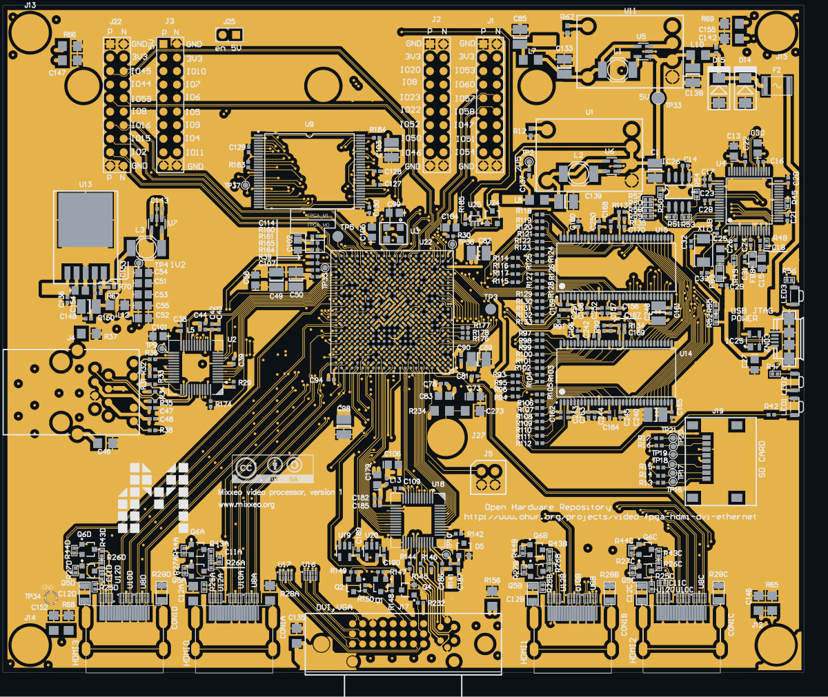
VIDEO FPGA HDMI DVI ETHERNET (OHWR0028 R1) is an open-hardware circuit board from the CERN Open Hardware Repository, designed in Altium Designer: a 6-layer board of 150.3 × 125.3 mm with 503 components and 475 nets, published under CERN-OHL-1.1.
review 87% walked · 21 findings: 2 blocker · 11 major · 8 minor (184 items)
Open in the interactive viewerRead the full review
Design review
Probe recorded 21 findings: 2 blocker · 11 major · 8 minor (184 items) on this design. Each is shown here with its reasoning; the full review links every one to the pins, nets and datasheet pages it rests on.
- NetCopperSplitblockerOpen
1V2's copper is in 2 pieces: C50.1 is not connected to the rest of the net
1V2's copper is in 2 pieces: C50.1 is not connected to the rest of the net. Piece 1: C151.2, C49.1, C51.1, C52.1, C53.1, C54.1, C55.1, C56.1 and 34 more pin(s), on TOP, IN1, IN2 and BOTTOM, 34 drill(s), 432.43 mm2 of pour, over (-1.4, -56.06) to (56.8, -39.06). Piece 2: C50.1, on TOP, over (33.51, -46.4) to (36.21, -44.8). The export files every one of these pins under the net, so every connectivity check passes; the copper the fab builds leaves them apart. Usually a pour island that touches only one via of its own net, or a track ending short of its copper: join the piece to the net and export again.
At split:1V2
- NetCopperSplitblockerOpen
NetCopperSplit: 5 boards×5
e.g. “DVI-I_SHIELD's copper is in 4 pieces: R156.2 and 2 other piece(s) are not connected to the rest of the net” · 5 different statements
At split:DVI-I_SHIELD, split:ETHSHIELD, split:NETC147_2, split:NETC152_2, split:NETC155_2
Each finding, with its own headline
split:DVI-I_SHIELDDVI-I_SHIELD's copper is in 4 pieces: R156.2 and 2 other piece(s) are not connected to the rest of the net
DVI-I_SHIELD's copper is in 4 pieces: R156.2 and 2 other piece(s) are not connected to the rest of the net. Piece 1: C135.2, on TOP, IN1, IN2 and BOTTOM, 5 drill(s), 48.63 mm2 of pour, over (34.1, -117.55) to (46.25, -111.26). Piece 2: R156.2, on TOP, IN1, IN2 and BOTTOM, 2 drill(s), over (70.79, -107.32) to (72.59, -104.74). Piece 3: J17.25, on TOP, IN1, IN2 and BOTTOM, 1 drill(s), over (37.73, -114.54) to (41.54, -110.73). Piece 4: J17.26, on TOP, IN1, IN2 and BOTTOM, 1 drill(s), over (68.46, -114.54) to (72.27, -110.73). The export files every one of these pins under the net, so every connectivity check passes; the copper the fab builds leaves them apart. Usually a pour island that touches only one via of its own net, or a track ending short of its copper: join the piece to the net and export again.
split:ETHSHIELDETHSHIELD's copper is in 3 pieces: J4.13 and 1 other piece(s) are not connected to the rest of the net
ETHSHIELD's copper is in 3 pieces: J4.13 and 1 other piece(s) are not connected to the rest of the net. Piece 1: C46.2 and J4.14, on TOP, IN1, IN2 and BOTTOM, 1 drill(s), over (-7.22, -75.83) to (-1.55, -72.17). Piece 2: J4.13, on TOP, IN1, IN2 and BOTTOM, 1 drill(s), over (-7.22, -58.56) to (-5.09, -56.43). Piece 3: R37.2, on TOP, over (-6.2, -55.26) to (-4.6, -53.46). The export files every one of these pins under the net, so every connectivity check passes; the copper the fab builds leaves them apart. Usually a pour island that touches only one via of its own net, or a track ending short of its copper: join the piece to the net and export again.
split:NETC147_2NETC147_2's copper is in 2 pieces: C147.2 is not connected to the rest of the net
NETC147_2's copper is in 2 pieces: C147.2 is not connected to the rest of the net. Piece 1: J13.1 and R66.2, on TOP, IN1, IN2 and BOTTOM, 2 drill(s), 2.19 mm2 of pour, over (-18.5, -1.59) to (-8.15, 5.64). Piece 2: C147.2, on TOP, IN1, IN2 and BOTTOM, 1 drill(s), over (-10.6, -3.95) to (-8.15, -2.15). The export files every one of these pins under the net, so every connectivity check passes; the copper the fab builds leaves them apart. Usually a pour island that touches only one via of its own net, or a track ending short of its copper: join the piece to the net and export again.
split:NETC152_2NETC152_2's copper is in 3 pieces: C152.2 and 1 other piece(s) are not connected to the rest of the net
NETC152_2's copper is in 3 pieces: C152.2 and 1 other piece(s) are not connected to the rest of the net. Piece 1: R68.2, on TOP, over (-8.68, -110.89) to (-6.88, -109.29). Piece 2: C152.2, on TOP, over (-11.48, -110.89) to (-9.68, -109.29). Piece 3: J14.1, on TOP, IN1, IN2 and BOTTOM, 1 drill(s), over (-18.5, -116.36) to (-10.22, -109.36). The export files every one of these pins under the net, so every connectivity check passes; the copper the fab builds leaves them apart. Usually a pour island that touches only one via of its own net, or a track ending short of its copper: join the piece to the net and export again.
split:NETC155_2NETC155_2's copper is in 2 pieces: C155.2 is not connected to the rest of the net
NETC155_2's copper is in 2 pieces: C155.2 is not connected to the rest of the net. Piece 1: J15.1 and R69.2, on TOP, IN1, IN2 and BOTTOM, 3 drill(s), 2.52 mm2 of pour, over (117.25, -1.36) to (128.5, 5.64). Piece 2: C155.2, on TOP, IN1, IN2 and BOTTOM, 1 drill(s), over (117.25, 0.11) to (119.95, 1.91). The export files every one of these pins under the net, so every connectivity check passes; the copper the fab builds leaves them apart. Usually a pour island that touches only one via of its own net, or a track ending short of its copper: join the piece to the net and export again.
- ReferencePlaneDiscontinuitymajorOpen
155 nets change reference between 3V3 and GND at 267 vias; 57 of them partial (fastest: DVI-I_B_N at 100 ps 10-90 %, ASSUMED)
At 267 via(s), on 155 net(s), the signal leaves a layer referenced by one of 3V3 and GND for a layer referenced by the other, and no plane references both layers. Different nets: no via can carry the return across; only decoupling between the two planes near the via can. The capacitor carrying the return across was measured at each via, at the knee of the crossing net's edge against 50 ohm assumed: 2 served, 265 with none. 267 of them at an ASSUMED edge (no edge on file for the net): state one (net_timing_state) and it is re-read. One decision covers the pair: whether 3V3 and GND are decoupled to each other near these vias. A via whose layers have more references than these two is a site of each pair it joins. 57 of them are partial: another reference continues across through a stitching via of its net, so only part of the return has nowhere to go. The pure ones are listed first, then the partial ones with the farthest stitching via first.
- 'HDMI2_SCL' at (97.28, -99.32), TOP -> BOTTOM: GND on GND to 3V3 on PWR; pure, no reference continues across; stitching none, 103.1 mm of track past the via on BOTTOM: At the 5 GHz knee of a 100 ps edge (10 ns 10-90 %, assumed: no edge is on file for the net) no capacitor carries the return; only the planes do. 3V3 and GND are not a thin pair (at most 0.2 mm), so their own capacitance does not carry the return. To serve it, change layers across the same plane, or move the signal to a layer referenced to ground. None.
- 'HDMI2_SCL' at (47.88, -59.31), TOP -> BOTTOM: GND on GND to 3V3 on PWR; pure, no reference continues across; stitching none, 103.1 mm of track past the via on BOTTOM: At the 5 GHz knee of a 100 ps edge (10 ns 10-90 %, assumed: no edge is on file for the net) no capacitor carries the return; only the planes do. 3V3 and GND are not a thin pair (at most 0.2 mm), so their own capacitance does not carry the return. To serve it, change layers across the same plane, or move the signal to a layer referenced to ground. Measured for reference: C74 (470 nF 0402) 1.9 mm away: 1.15 nH in the 1.070 mm cavity + 0.30 nH ESL + 1.16 nH mounting (pad 0.07 nH (vias beside the pads) + 1 via pair(s) at 1.00 mm pitch, 0.20 mm drill, 1.18 mm to the farther plane): 81.8 ohm at the knee, 164 % of 50 ohm (assumed track impedance). None.
- 'SD_DAT0' at (101.73, -75.44), TOP -> IN2: GND on GND to GND on IN1, 3V3 on PWR; partial, GND continues through a via of GND 4.78 mm away; stitching none, 102.4 mm of track past the via on IN2: At the 5 GHz knee of a 100 ps edge (100 ps 10-90 %, assumed: no edge is on file for the net) no capacitor carries the return; only the planes do. 3V3 and GND are not a thin pair (at most 0.2 mm), so their own capacitance does not carry the return. To serve it, change layers across the same plane, or move the signal to a layer referenced to ground. None.
- 'SD_DAT1' at (101.22, -76.41), TOP -> IN2: GND on GND to GND on IN1, 3V3 on PWR; partial, GND continues through a via of GND 3.69 mm away; stitching none, 101.1 mm of track past the via on IN2: At the 5 GHz knee of a 100 ps edge (100 ps 10-90 %, assumed: no edge is on file for the net) no capacitor carries the return; only the planes do. 3V3 and GND are not a thin pair (at most 0.2 mm), so their own capacitance does not carry the return. To serve it, change layers across the same plane, or move the signal to a layer referenced to ground. None.
- 'SD_DAT3' at (101.86, -78.03), TOP -> IN2: GND on GND to GND on IN1, 3V3 on PWR; partial, GND continues through a via of GND 2.7 mm away; stitching none, 96.8 mm of track past the via on IN2: At the 5 GHz knee of a 100 ps edge (100 ps 10-90 %, assumed: no edge is on file for the net) no capacitor carries the return; only the planes do. 3V3 and GND are not a thin pair (at most 0.2 mm), so their own capacitance does not carry the return. To serve it, change layers across the same plane, or move the signal to a layer referenced to ground. None.
- 'SD_DAT2' at (101.25, -78.69), TOP -> IN2: GND on GND to GND on IN1, 3V3 on PWR; partial, GND continues through a via of GND 1.81 mm away; stitching none, 93.9 mm of track past the via on IN2: At the 5 GHz knee of a 100 ps edge (100 ps 10-90 %, assumed: no edge is on file for the net) no capacitor carries the return; only the planes do. 3V3 and GND are not a thin pair (at most 0.2 mm), so their own capacitance does not carry the return. To serve it, change layers across the same plane, or move the signal to a layer referenced to ground. None.
- 'SD_CLK' at (104.12, -77.07), TOP -> IN2: GND on GND to GND on IN1, 3V3 on PWR; partial, GND continues through a via of GND 5.09 mm away; stitching none, 93.8 mm of track past the via on IN2: At the 5 GHz knee of a 100 ps edge (1 ns 10-90 %, assumed: no edge is on file for the net) no capacitor carries the return; only the planes do. 3V3 and GND are not a thin pair (at most 0.2 mm), so their own capacitance does not carry the return. To serve it, change layers across the same plane, or move the signal to a layer referenced to ground. None.
- 'HDMI2_TMDS0_N' at (53.88, -42.3), TOP -> IN2: GND on GND to 3V3 on PWR; pure, no reference continues across; stitching none, 92.5 mm of track past the via on IN2: At the 5 GHz knee of a 100 ps edge (100 ps 10-90 %, assumed: no edge is on file for the net) no capacitor carries the return; only the planes do. 3V3 and GND are not a thin pair (at most 0.2 mm), so their own capacitance does not carry the return. To serve it, change layers across the same plane, or move the signal to a layer referenced to ground. None.
- 'HDMI2_TMDS0_N' at (99.93, -87.94), TOP -> IN2: GND on GND to GND on IN1, 3V3 on PWR; partial, GND continues through a via of GND 1.9 mm away; stitching none, 92.5 mm of track past the via on IN2: At the 5 GHz knee of a 100 ps edge (100 ps 10-90 %, assumed: no edge is on file for the net) no capacitor carries the return; only the planes do. 3V3 and GND are not a thin pair (at most 0.2 mm), so their own capacitance does not carry the return. To serve it, change layers across the same plane, or move the signal to a layer referenced to ground. None.
- 'HDMI2_TMDS0_P' at (53.88, -43.31), TOP -> IN2: GND on GND to 3V3 on PWR; pure, no reference continues across; stitching none, 92.2 mm of track past the via on IN2: At the 5 GHz knee of a 100 ps edge (100 ps 10-90 %, assumed: no edge is on file for the net) no capacitor carries the return; only the planes do. 3V3 and GND are not a thin pair (at most 0.2 mm), so their own capacitance does not carry the return. To serve it, change layers across the same plane, or move the signal to a layer referenced to ground. None.
- 'HDMI2_TMDS0_P' at (99.48, -87.5), TOP -> IN2: GND on GND to GND on IN1, 3V3 on PWR; partial, GND continues through a via of GND 2.37 mm away; stitching none, 92.2 mm of track past the via on IN2: At the 5 GHz knee of a 100 ps edge (100 ps 10-90 %, assumed: no edge is on file for the net) no capacitor carries the return; only the planes do. 3V3 and GND are not a thin pair (at most 0.2 mm), so their own capacitance does not carry the return. To serve it, change layers across the same plane, or move the signal to a layer referenced to ground. None.
- 'HDMI2_TMDS_CLK_N' at (104.68, -90.91), TOP -> IN2: GND on GND to GND on IN1, 3V3 on PWR; partial, GND continues through a via of GND 3.93 mm away; stitching none, 92.1 mm of track past the via on IN2: At the 5 GHz knee of a 100 ps edge (1 ns 10-90 %, assumed: no edge is on file for the net) no capacitor carries the return; only the planes do. 3V3 and GND are not a thin pair (at most 0.2 mm), so their own capacitance does not carry the return. To serve it, change layers across the same plane, or move the signal to a layer referenced to ground. None.
- and 255 more
Every site is a row of this finding's evidence, keyed by net, layers and position. GET /api/odb/boards/30/reference-planes?group=refchange%3A3V3%7CGND serves each with its own layer_image region; all of them lie in x -3.56..114.73, y -104.76..-4.81 mm (board frame, Y up).
The reference on each layer is the first plane the track meets leaving the via, anti-pads and the net's own copper skipped. Whether it matters depends on each signal's edge rate, which nothing on file states for these nets: a slow static line crosses a split harmlessly, a fast edge does not.
At refchange:3V3|GND
- DecapOrdermajorOpen
DecapOrder: 3 findings (2 components, 1 pin)×3
3 checked by the review by Claude walker W4 (Cern session) — 3 different reasons
At U14, U15, U22.R21
Each finding, with its own headline
U14U14 supply pins 3, 55 on '2V5': the smallest capacitor C163 sits 4.3 mm away, behind C243 at 1.8 mm
U14 supply pins 3, 55 on '2V5': the smallest capacitor C163 sits 4.3 mm away, behind C243 at 1.8 mm. U14.3: the smallest value, C163 (10 nF), is 4.3 mm from the pin and C243 (100 nF) 1.8 mm: the high-frequency part sits behind more inductance than the bulk part, which needs it least. U14.55: the smallest value, C166 (10 nF), is 4.2 mm from the pin and C242 (100 nF) 1.3 mm: the high-frequency part sits behind more inductance than the bulk part, which needs it least. Swap them, or bring the smallest value to the pin: it serves the fastest current and is the one the loop inductance defeats. Distances are pad centre to pin centre in the board plane. The 5 mm radius, the 10x value step and the 1 mm / 1.5x tie tolerance are Probe's starting values.
U15U15 supply pins 15, 55 on '2V5': the smallest capacitor C158 sits 4.6 mm away, behind C157 at 2.1 mm
U15 supply pins 15, 55 on '2V5': the smallest capacitor C158 sits 4.6 mm away, behind C157 at 2.1 mm. U15.15: the smallest value, C158 (10 nF), is 4.6 mm from the pin and C157 (100 nF) 2.1 mm: the high-frequency part sits behind more inductance than the bulk part, which needs it least. U15.55: the smallest value, C160 (10 nF), is 4.4 mm from the pin and C250 (100 nF) 2.1 mm: the high-frequency part sits behind more inductance than the bulk part, which needs it least. Swap them, or bring the smallest value to the pin: it serves the fastest current and is the one the loop inductance defeats. Distances are pad centre to pin centre in the board plane. The 5 mm radius, the 10x value step and the 1 mm / 1.5x tie tolerance are Probe's starting values.
U22.R21U22 supply pin R21 on '3V3': the smallest capacitor C113 sits 3.5 mm away, behind C86 at 0.4 mm
U22 supply pin R21 on '3V3': the smallest capacitor C113 sits 3.5 mm away, behind C86 at 0.4 mm. U22.R21: the smallest value, C113 (470 nF), is 3.5 mm from the pin and C86 (4.7 uF) 0.4 mm: the high-frequency part sits behind more inductance than the bulk part, which needs it least. Swap them, or bring the smallest value to the pin: it serves the fastest current and is the one the loop inductance defeats. Distances are pad centre to pin centre in the board plane. The 5 mm radius, the 10x value step and the 1 mm / 1.5x tie tolerance are Probe's starting values.
- DecapViaFanoutmajorOpen
DecapViaFanout: 9 components×9
9 checked by the review by Claude walker W4 (Cern session) — 9 different reasons
At C100, C10B, C10D, C117, C136, C137 and 3 more
Each finding, with its own headline
C100C100 on '3V3': its rail pad reaches its via over 2.26 mm of track, adding about 0.68 nH to its loop, past Probe's 0.5 nH starting value; put the vias at the pads
C100 on '3V3': its rail pad reaches its via over 2.26 mm of track, adding about 0.68 nH to its loop, past Probe's 0.5 nH starting value; put the vias at the pads. C100.1 (rail) runs 2.26 mm along its copper to its nearest via, 1.26 mm past the 1 mm beside the pad: 0.68 nH; C100.2 (ground) not measured: the pad sits in a pour of its net on its own layer, which has no track length to measure. Each run past the pad as one conductor of a pair 1.90 mm apart (the pad pitch), 0.2 l ln(D/R) nH with R 0.127 mm (the track's width is not read): 0.68 nH in all. Put the vias at the pads (or in them), one per pad at least, the rail's and the ground's close together; the capacitor's own inductance as mounted is 0.68 nH (pad 0.10 nH + no via of the first net within 1 mm of its pad: the study's 0.6 nH per mm of 0.11 mm depth, ASSUMED). 0.5 nH is Probe's starting value, about the whole mounted inductance of a well-mounted 0402.
C10BC10B on '3V3': its rail pad reaches its via over 2.90 mm of track, adding about 0.74 nH to its loop, past Probe's 0.5 nH starting value; put the vias at the pads
C10B on '3V3': its rail pad reaches its via over 2.90 mm of track, adding about 0.74 nH to its loop, past Probe's 0.5 nH starting value; put the vias at the pads. C10B.2 (rail) runs 2.90 mm along its copper to its nearest via, 1.90 mm past the 1 mm beside the pad: 0.74 nH; C10B.1 (ground) not measured: the pad sits in a pour of its net on its own layer, which has no track length to measure. Each run past the pad as one conductor of a pair 0.90 mm apart (the pad pitch), 0.2 l ln(D/R) nH with R 0.127 mm (the track's width is not read): 0.74 nH in all. Put the vias at the pads (or in them), one per pad at least, the rail's and the ground's close together; the capacitor's own inductance as mounted is 0.44 nH (pad 0.07 nH + no via of the first net within 1 mm of its pad: the study's 0.6 nH per mm of 0.11 mm depth, ASSUMED). 0.5 nH is Probe's starting value, about the whole mounted inductance of a well-mounted 0402.
C10DC10D on '3V3': its rail pad reaches its via over 3.80 mm of track, adding about 1.10 nH to its loop, past Probe's 0.5 nH starting value; put the vias at the pads
C10D on '3V3': its rail pad reaches its via over 3.80 mm of track, adding about 1.10 nH to its loop, past Probe's 0.5 nH starting value; put the vias at the pads. C10D.2 (rail) runs 3.80 mm along its copper to its nearest via, 2.80 mm past the 1 mm beside the pad: 1.10 nH; C10D.1 (ground) not measured: the pad sits in a pour of its net on its own layer, which has no track length to measure. Each run past the pad as one conductor of a pair 0.90 mm apart (the pad pitch), 0.2 l ln(D/R) nH with R 0.127 mm (the track's width is not read): 1.10 nH in all. Put the vias at the pads (or in them), one per pad at least, the rail's and the ground's close together; the capacitor's own inductance as mounted is 0.44 nH (pad 0.07 nH + no via of the first net within 1 mm of its pad: the study's 0.6 nH per mm of 0.11 mm depth, ASSUMED). 0.5 nH is Probe's starting value, about the whole mounted inductance of a well-mounted 0402.
C117C117 on '3V3': its rail pad reaches its via over 3.71 mm of track, adding about 1.13 nH to its loop, past Probe's 0.5 nH starting value; put the vias at the pads
C117 on '3V3': its rail pad reaches its via over 3.71 mm of track, adding about 1.13 nH to its loop, past Probe's 0.5 nH starting value; put the vias at the pads. C117.2 (rail) runs 3.71 mm along its copper to its nearest via, 2.71 mm past the 1 mm beside the pad: 1.13 nH; C117.1 (ground) not measured: the pad sits in a pour of its net on its own layer, which has no track length to measure. Each run past the pad as one conductor of a pair 1.02 mm apart (the pad pitch), 0.2 l ln(D/R) nH with R 0.127 mm (the track's width is not read): 1.13 nH in all. Put the vias at the pads (or in them), one per pad at least, the rail's and the ground's close together; the capacitor's own inductance as mounted is 0.44 nH (pad 0.07 nH + no via of the first net within 1 mm of its pad: the study's 0.6 nH per mm of 0.11 mm depth, ASSUMED). 0.5 nH is Probe's starting value, about the whole mounted inductance of a well-mounted 0402.
C136C136 on 'NETC136_2': its rail pad reaches its via over 3.04 mm of track, adding about 0.85 nH to its loop, past Probe's 0.5 nH starting value; put the vias at the pads
C136 on 'NETC136_2': its rail pad reaches its via over 3.04 mm of track, adding about 0.85 nH to its loop, past Probe's 0.5 nH starting value; put the vias at the pads. C136.2 (rail) runs 3.04 mm along its copper to its nearest via, 2.04 mm past the 1 mm beside the pad: 0.85 nH; C136.1 (ground) not measured: the pad sits in a pour of its net on its own layer, which has no track length to measure. Each run past the pad as one conductor of a pair 1.02 mm apart (the pad pitch), 0.2 l ln(D/R) nH with R 0.127 mm (the track's width is not read): 0.85 nH in all. Put the vias at the pads (or in them), one per pad at least, the rail's and the ground's close together; the capacitor's own inductance as mounted is 0.44 nH (pad 0.07 nH + no via of the first net within 1 mm of its pad: the study's 0.6 nH per mm of 0.11 mm depth, ASSUMED). 0.5 nH is Probe's starting value, about the whole mounted inductance of a well-mounted 0402.
C137C137 on '2V5': its rail pad reaches its via over 6.00 mm of track, adding about 2.08 nH to its loop, past Probe's 0.5 nH starting value; put the vias at the pads
C137 on '2V5': its rail pad reaches its via over 6.00 mm of track, adding about 2.08 nH to its loop, past Probe's 0.5 nH starting value; put the vias at the pads. C137.2 (rail) runs at least 6.00 mm along its copper to its nearest via, 5.00 mm past the 1 mm beside the pad: 2.08 nH; C137.1 (ground) not measured: the pad sits in a pour of its net on its own layer, which has no track length to measure. Each run past the pad as one conductor of a pair 1.02 mm apart (the pad pitch), 0.2 l ln(D/R) nH with R 0.127 mm (the track's width is not read): 2.08 nH in all. Put the vias at the pads (or in them), one per pad at least, the rail's and the ground's close together; the capacitor's own inductance as mounted is 1.14 nH (pad 0.07 nH + no via of the first net within 1 mm of its pad: the study's 0.6 nH per mm of 1.29 mm depth, ASSUMED). 0.5 nH is Probe's starting value, about the whole mounted inductance of a well-mounted 0402.
C14C14 on '3V3': its rail pad reaches its via over 3.59 mm of track, adding about 1.08 nH to its loop, past Probe's 0.5 nH starting value; put the vias at the pads
C14 on '3V3': its rail pad reaches its via over 3.59 mm of track, adding about 1.08 nH to its loop, past Probe's 0.5 nH starting value; put the vias at the pads. C14.2 (rail) runs 3.59 mm along its copper to its nearest via, 2.59 mm past the 1 mm beside the pad: 1.08 nH; C14.1 (ground) not measured: the pad sits in a pour of its net on its own layer, which has no track length to measure. Each run past the pad as one conductor of a pair 1.02 mm apart (the pad pitch), 0.2 l ln(D/R) nH with R 0.127 mm (the track's width is not read): 1.08 nH in all. Put the vias at the pads (or in them), one per pad at least, the rail's and the ground's close together; the capacitor's own inductance as mounted is 1.14 nH (pad 0.07 nH + no via of the first net within 1 mm of its pad: the study's 0.6 nH per mm of 1.29 mm depth, ASSUMED). 0.5 nH is Probe's starting value, about the whole mounted inductance of a well-mounted 0402.
C31C31 on '3V3': its rail pad reaches its via over 2.64 mm of track, adding about 0.68 nH to its loop, past Probe's 0.5 nH starting value; put the vias at the pads
C31 on '3V3': its rail pad reaches its via over 2.64 mm of track, adding about 0.68 nH to its loop, past Probe's 0.5 nH starting value; put the vias at the pads. C31.2 (rail) runs 2.64 mm along its copper to its nearest via, 1.64 mm past the 1 mm beside the pad: 0.68 nH; C31.1 (ground) not measured: the pad sits in a pour of its net on its own layer, which has no track length to measure. Each run past the pad as one conductor of a pair 1.02 mm apart (the pad pitch), 0.2 l ln(D/R) nH with R 0.127 mm (the track's width is not read): 0.68 nH in all. Put the vias at the pads (or in them), one per pad at least, the rail's and the ground's close together; the capacitor's own inductance as mounted is 1.14 nH (pad 0.07 nH + no via of the first net within 1 mm of its pad: the study's 0.6 nH per mm of 1.29 mm depth, ASSUMED). 0.5 nH is Probe's starting value, about the whole mounted inductance of a well-mounted 0402.
C88C88 on '3V3': its rail pad reaches its via over 6.00 mm of track, adding about 2.71 nH to its loop, past Probe's 0.5 nH starting value; put the vias at the pads
C88 on '3V3': its rail pad reaches its via over 6.00 mm of track, adding about 2.71 nH to its loop, past Probe's 0.5 nH starting value; put the vias at the pads. C88.1 (rail) runs at least 6.00 mm along its copper to its nearest via, 5.00 mm past the 1 mm beside the pad: 2.71 nH; C88.2 (ground) not measured: the pad sits in a pour of its net on its own layer, which has no track length to measure. Each run past the pad as one conductor of a pair 1.90 mm apart (the pad pitch), 0.2 l ln(D/R) nH with R 0.127 mm (the track's width is not read): 2.71 nH in all. Put the vias at the pads (or in them), one per pad at least, the rail's and the ground's close together; the capacitor's own inductance as mounted is 0.68 nH (pad 0.10 nH + no via of the first net within 1 mm of its pad: the study's 0.6 nH per mm of 0.11 mm depth, ASSUMED). 0.5 nH is Probe's starting value, about the whole mounted inductance of a well-mounted 0402.
- EsdProtectorPlacementmajorOpen
EsdProtectorPlacement: 18 components×18
18 checked by the review by Claude walker W4 (Cern session) — 3 different reasons
At IC25, U21, U23
Each finding, with its own headline
IC25IC25.2 on 'USB_N': IC25.2 hangs 1.08 mm off the line (limit 1 mm, default
IC25 (PRTR5V0U2X) protects 'USB_N' at CON2.2. Along the copper: 4.06 mm of track from the contact, 0 via(s) before it, on a 1.08 mm branch off the line; the line runs 28.02 mm on to U4.7; IC25 sits 1.68 mm farther from the contact than the nearest place outside CON2.
IC25.2 hangs 1.08 mm off the line (limit 1 mm, default: no datasheet figure on file): the line carries the strike past it while the clamp is reached through the branch.
Measured on the copper the ODB states: tracks, the pads they land on, and the netlist's vias. Not a straight line between centroids.
IC25IC25.4 on '5V_USB': 4 via(s) between CON2.1 and IC25.4
IC25 (PRTR5V0U2X) protects '5V_USB' at CON2.1. Along the copper: 12.95 mm of track from the contact, 4 via(s) before it, on a 8.5 mm branch off the line; the line runs 5.39 mm on to C27.1; IC25 sits 1.68 mm farther from the contact than the nearest place outside CON2.
4 via(s) between CON2.1 and IC25.4: the strike reaches an inner layer before it is clamped. IC25.4 hangs 8.5 mm off the line (limit 1 mm, default: no datasheet figure on file): the line carries the strike past it while the clamp is reached through the branch. IC25 joins the line 4.45 mm from CON2.1 on a 5.39 mm run to C27.1: nearer the far end than the contact, so the surge travels most of the line before it is clamped.
Measured on the copper the ODB states: tracks, the pads they land on, and the netlist's vias. Not a straight line between centroids.
U21U21.1 on 'A_VSYNC': U21.1 hangs 6.6 mm off the line (limit 1 mm, default
U21 (RCLAMP0524P.TCT) protects 'A_VSYNC' at J17.8. Along the copper: 6.6 mm of track from the contact, 0 via(s) before it, on a 6.6 mm branch off the line; the line runs 19.41 mm on to U20.4; U21 sits at J17, within 1.09 mm of the nearest place outside it to the contact: the track to it is mostly the escape out of J17's own pins, which no placement shortens.
U21.1 hangs 6.6 mm off the line (limit 1 mm, default: no datasheet figure on file): the line carries the strike past it while the clamp is reached through the branch.
Measured on the copper the ODB states: tracks, the pads they land on, and the netlist's vias. Not a straight line between centroids.
U21U21.10 on 'A_VSYNC': U21.10 hangs 5.73 mm off the line (limit 1 mm, default
U21 (RCLAMP0524P.TCT) protects 'A_VSYNC' at J17.8. Along the copper: 5.73 mm of track from the contact, 0 via(s) before it, on a 5.73 mm branch off the line; the line runs 19.41 mm on to U20.4; U21 sits at J17, within 1.09 mm of the nearest place outside it to the contact: the track to it is mostly the escape out of J17's own pins, which no placement shortens.
U21.10 hangs 5.73 mm off the line (limit 1 mm, default: no datasheet figure on file): the line carries the strike past it while the clamp is reached through the branch.
Measured on the copper the ODB states: tracks, the pads they land on, and the netlist's vias. Not a straight line between centroids.
U21U21.2 on 'HPD': U21.2 hangs 9.32 mm off the line (limit 1 mm, default
U21 (RCLAMP0524P.TCT) protects 'HPD' at J17.16. Along the copper: 9.32 mm of track from the contact, 0 via(s) before it, on a 9.32 mm branch off the line; the line runs 6.27 mm on to R232.2; U21 sits at J17, within 0.72 mm of the nearest place outside it to the contact: the track to it is mostly the escape out of J17's own pins, which no placement shortens.
U21.2 hangs 9.32 mm off the line (limit 1 mm, default: no datasheet figure on file): the line carries the strike past it while the clamp is reached through the branch.
Measured on the copper the ODB states: tracks, the pads they land on, and the netlist's vias. Not a straight line between centroids.
U21U21.4 on 'DDC_DATA': U21.4 hangs 7.11 mm off the line (limit 1 mm, default
U21 (RCLAMP0524P.TCT) protects 'DDC_DATA' at J17.7. Along the copper: 7.11 mm of track from the contact, 0 via(s) before it, on a 7.11 mm branch off the line; the line runs 7.86 mm on to R148.1; U21 sits 2.66 mm farther from the contact than the nearest place outside J17.
U21.4 hangs 7.11 mm off the line (limit 1 mm, default: no datasheet figure on file): the line carries the strike past it while the clamp is reached through the branch.
Measured on the copper the ODB states: tracks, the pads they land on, and the netlist's vias. Not a straight line between centroids.
U21U21.5 on 'DDC_CLK': U21.5 hangs 8.51 mm off the line (limit 1 mm, default
U21 (RCLAMP0524P.TCT) protects 'DDC_CLK' at J17.6. Along the copper: 8.51 mm of track from the contact, 0 via(s) before it, on a 8.51 mm branch off the line; the line runs 10.29 mm on to R150.2; U21 sits 4.42 mm farther from the contact than the nearest place outside J17.
U21.5 hangs 8.51 mm off the line (limit 1 mm, default: no datasheet figure on file): the line carries the strike past it while the clamp is reached through the branch.
Measured on the copper the ODB states: tracks, the pads they land on, and the netlist's vias. Not a straight line between centroids.
U21U21.6 on 'DDC_CLK': U21.6 hangs 7.64 mm off the line (limit 1 mm, default
U21 (RCLAMP0524P.TCT) protects 'DDC_CLK' at J17.6. Along the copper: 7.64 mm of track from the contact, 0 via(s) before it, on a 7.64 mm branch off the line; the line runs 10.29 mm on to R150.2; U21 sits 4.42 mm farther from the contact than the nearest place outside J17.
U21.6 hangs 7.64 mm off the line (limit 1 mm, default: no datasheet figure on file): the line carries the strike past it while the clamp is reached through the branch.
Measured on the copper the ODB states: tracks, the pads they land on, and the netlist's vias. Not a straight line between centroids.
U21U21.7 on 'DDC_DATA': U21.7 hangs 6.24 mm off the line (limit 1 mm, default
U21 (RCLAMP0524P.TCT) protects 'DDC_DATA' at J17.7. Along the copper: 6.24 mm of track from the contact, 0 via(s) before it, on a 6.24 mm branch off the line; the line runs 7.86 mm on to R148.1; U21 sits 2.66 mm farther from the contact than the nearest place outside J17.
U21.7 hangs 6.24 mm off the line (limit 1 mm, default: no datasheet figure on file): the line carries the strike past it while the clamp is reached through the branch.
Measured on the copper the ODB states: tracks, the pads they land on, and the netlist's vias. Not a straight line between centroids.
U21U21.9 on 'HPD': U21.9 hangs 8.45 mm off the line (limit 1 mm, default
U21 (RCLAMP0524P.TCT) protects 'HPD' at J17.16. Along the copper: 8.45 mm of track from the contact, 0 via(s) before it, on a 8.45 mm branch off the line; the line runs 6.27 mm on to R232.2; U21 sits at J17, within 0.72 mm of the nearest place outside it to the contact: the track to it is mostly the escape out of J17's own pins, which no placement shortens.
U21.9 hangs 8.45 mm off the line (limit 1 mm, default: no datasheet figure on file): the line carries the strike past it while the clamp is reached through the branch.
Measured on the copper the ODB states: tracks, the pads they land on, and the netlist's vias. Not a straight line between centroids.
U23U23.1 on 'A_HSYNC': U23.1 hangs 6.6 mm off the line (limit 1 mm, default
U23 (RCLAMP0524P.TCT) protects 'A_HSYNC' at J17.C4. Along the copper: 6.6 mm of track from the contact, 0 via(s) before it, on a 6.6 mm branch off the line; the line runs 33.41 mm on to U19.4; U23 sits at J17, within 0 mm of the nearest place outside it to the contact: the track to it is mostly the escape out of J17's own pins, which no placement shortens.
U23.1 hangs 6.6 mm off the line (limit 1 mm, default: no datasheet figure on file): the line carries the strike past it while the clamp is reached through the branch.
Measured on the copper the ODB states: tracks, the pads they land on, and the netlist's vias. Not a straight line between centroids.
U23U23.10 on 'A_HSYNC': U23.10 hangs 5.73 mm off the line (limit 1 mm, default
U23 (RCLAMP0524P.TCT) protects 'A_HSYNC' at J17.C4. Along the copper: 5.73 mm of track from the contact, 0 via(s) before it, on a 5.73 mm branch off the line; the line runs 33.41 mm on to U19.4; U23 sits at J17, within 0 mm of the nearest place outside it to the contact: the track to it is mostly the escape out of J17's own pins, which no placement shortens.
U23.10 hangs 5.73 mm off the line (limit 1 mm, default: no datasheet figure on file): the line carries the strike past it while the clamp is reached through the branch.
Measured on the copper the ODB states: tracks, the pads they land on, and the netlist's vias. Not a straight line between centroids.
U23U23.2 on 'ANALOG_B': U23.2 hangs 8.69 mm off the line (limit 1 mm, default
U23 (RCLAMP0524P.TCT) protects 'ANALOG_B' at J17.C3. Along the copper: 8.69 mm of track from the contact, 0 via(s) before it, on a 8.69 mm branch off the line; the line runs 16.91 mm on to R144.2; U23 sits at J17, within 0.04 mm of the nearest place outside it to the contact: the track to it is mostly the escape out of J17's own pins, which no placement shortens.
U23.2 hangs 8.69 mm off the line (limit 1 mm, default: no datasheet figure on file): the line carries the strike past it while the clamp is reached through the branch.
Measured on the copper the ODB states: tracks, the pads they land on, and the netlist's vias. Not a straight line between centroids.
U23U23.4 on 'ANALOG_G': U23.4 hangs 3.42 mm off the line (limit 1 mm, default
U23 (RCLAMP0524P.TCT) protects 'ANALOG_G' at J17.C2. Along the copper: 3.42 mm of track from the contact, 0 via(s) before it, on a 3.42 mm branch off the line; the line runs 17.67 mm on to R145.2; U23 sits at J17, within 0 mm of the nearest place outside it to the contact: the track to it is mostly the escape out of J17's own pins, which no placement shortens.
U23.4 hangs 3.42 mm off the line (limit 1 mm, default: no datasheet figure on file): the line carries the strike past it while the clamp is reached through the branch.
Measured on the copper the ODB states: tracks, the pads they land on, and the netlist's vias. Not a straight line between centroids.
U23U23.5 on 'ANALOG_R': U23.5 hangs 5.03 mm off the line (limit 1 mm, default
U23 (RCLAMP0524P.TCT) protects 'ANALOG_R' at J17.C1. Along the copper: 5.03 mm of track from the contact, 0 via(s) before it, on a 5.03 mm branch off the line; the line runs 12.62 mm on to R146.2; U23 sits at J17, within 0.52 mm of the nearest place outside it to the contact: the track to it is mostly the escape out of J17's own pins, which no placement shortens.
U23.5 hangs 5.03 mm off the line (limit 1 mm, default: no datasheet figure on file): the line carries the strike past it while the clamp is reached through the branch.
Measured on the copper the ODB states: tracks, the pads they land on, and the netlist's vias. Not a straight line between centroids.
U23U23.6 on 'ANALOG_R': U23.6 hangs 4.16 mm off the line (limit 1 mm, default
U23 (RCLAMP0524P.TCT) protects 'ANALOG_R' at J17.C1. Along the copper: 4.16 mm of track from the contact, 0 via(s) before it, on a 4.16 mm branch off the line; the line runs 12.62 mm on to R146.2; U23 sits at J17, within 0.52 mm of the nearest place outside it to the contact: the track to it is mostly the escape out of J17's own pins, which no placement shortens.
U23.6 hangs 4.16 mm off the line (limit 1 mm, default: no datasheet figure on file): the line carries the strike past it while the clamp is reached through the branch.
Measured on the copper the ODB states: tracks, the pads they land on, and the netlist's vias. Not a straight line between centroids.
U23U23.7 on 'ANALOG_G': U23.7 hangs 2.55 mm off the line (limit 1 mm, default
U23 (RCLAMP0524P.TCT) protects 'ANALOG_G' at J17.C2. Along the copper: 2.55 mm of track from the contact, 0 via(s) before it, on a 2.55 mm branch off the line; the line runs 17.67 mm on to R145.2; U23 sits at J17, within 0 mm of the nearest place outside it to the contact: the track to it is mostly the escape out of J17's own pins, which no placement shortens.
U23.7 hangs 2.55 mm off the line (limit 1 mm, default: no datasheet figure on file): the line carries the strike past it while the clamp is reached through the branch.
Measured on the copper the ODB states: tracks, the pads they land on, and the netlist's vias. Not a straight line between centroids.
U23U23.9 on 'ANALOG_B': U23.9 hangs 7.82 mm off the line (limit 1 mm, default
U23 (RCLAMP0524P.TCT) protects 'ANALOG_B' at J17.C3. Along the copper: 7.82 mm of track from the contact, 0 via(s) before it, on a 7.82 mm branch off the line; the line runs 16.91 mm on to R144.2; U23 sits at J17, within 0.04 mm of the nearest place outside it to the contact: the track to it is mostly the escape out of J17's own pins, which no placement shortens.
U23.9 hangs 7.82 mm off the line (limit 1 mm, default: no datasheet figure on file): the line carries the strike past it while the clamp is reached through the branch.
Measured on the copper the ODB states: tracks, the pads they land on, and the netlist's vias. Not a straight line between centroids.
- EsdProtectorPlacementmajorOpen
EsdProtectorPlacement: 2 components×2
Checked by the review, stands · Claude walker W4 (Cern session) — Checked (W4, fleet re-walk): the placement is measured from the copper as stated (U12B.4 on 'HDMI_P5VB': U12B.4 hangs 2.4 mm off the line (limit 1 mm, default; U12B.6 on 'HDMI_HPDB': U12B joins the line 3.27 mm from CON1B.19 on a 5.42 mm run to R25B.1; U12B.7 on 'HDMI_P5VB': U12B.7 hangs 3.27 mm off the line (limit 1 mm, default). Protector placement guidance (on the line, near the connector, no vias/stubs) is layout practice from protector app notes; its effect depends on the ESD event and the protected part's rating, not on file here. Left open for the owner.
At U12B
Each finding, with its own headline
U12BU12B.4 on 'HDMI_P5VB': U12B.4 hangs 2.4 mm off the line (limit 1 mm, default
U12B (RCLAMP0524P.TCT) protects 'HDMI_P5VB' at CON1B.18. Along the copper: 2.4 mm of track from the contact, 0 via(s) before it, on a 2.4 mm branch off the line; the line runs 2.87 mm on to C11B.1; U12B sits at CON1B, within 0.72 mm of the nearest place outside it to the contact: the track to it is mostly the escape out of CON1B's own pins, which no placement shortens.
U12B.4 hangs 2.4 mm off the line (limit 1 mm, default: no datasheet figure on file): the line carries the strike past it while the clamp is reached through the branch.
Measured on the copper the ODB states: tracks, the pads they land on, and the netlist's vias. Not a straight line between centroids.
U12BU12B.7 on 'HDMI_P5VB': U12B.7 hangs 3.27 mm off the line (limit 1 mm, default
U12B (RCLAMP0524P.TCT) protects 'HDMI_P5VB' at CON1B.18. Along the copper: 3.27 mm of track from the contact, 0 via(s) before it, on a 3.27 mm branch off the line; the line runs 2.87 mm on to C11B.1; U12B sits at CON1B, within 0.72 mm of the nearest place outside it to the contact: the track to it is mostly the escape out of CON1B's own pins, which no placement shortens.
U12B.7 hangs 3.27 mm off the line (limit 1 mm, default: no datasheet figure on file): the line carries the strike past it while the clamp is reached through the branch.
Measured on the copper the ODB states: tracks, the pads they land on, and the netlist's vias. Not a straight line between centroids.
- FiducialMissingmajorOpen
FiducialMissing: 2 boards×2
Checked by the review, stands · Claude walker (cern session) — Stands: no fiducial component on either side in the design data; recorded as OBS-299.
At bottom, top
Each finding, with its own headline
bottomThe bottom side carries 92 SMT component(s) and no fiducial was found on it
The bottom side carries 92 SMT component(s) but no fiducial was found on it — a placement machine has no optical reference to align to. Probe found no pad labelled .pad_usage=g_fiducial/l_fiducial (basis pad_usage); no single-pad, netless, undrilled component whose 0.5-3 mm round pad has a concentric solder-mask opening at least 1.5x its diameter with no other copper inside it (basis geometry); and no component whose refdes starts FID or whose part or package name contains FIDUCIAL (basis footprint-name). If your library names fiducials something Probe does not recognise, mark this benign — disposition_finding(rule='FiducialMissing', entity='bottom', status='benign', reason=…) — the name match only ever silences this check, it never asserts anything. If the side really has no fiducial, say so with status='confirmed': that answers the finding and keeps it gating release.
topThe top side carries 262 SMT component(s) and no fiducial was found on it
The top side carries 262 SMT component(s) but no fiducial was found on it — a placement machine has no optical reference to align to. Probe found no pad labelled .pad_usage=g_fiducial/l_fiducial (basis pad_usage); no single-pad, netless, undrilled component whose 0.5-3 mm round pad has a concentric solder-mask opening at least 1.5x its diameter with no other copper inside it (basis geometry); and no component whose refdes starts FID or whose part or package name contains FIDUCIAL (basis footprint-name). If your library names fiducials something Probe does not recognise, mark this benign — disposition_finding(rule='FiducialMissing', entity='top', status='benign', reason=…) — the name match only ever silences this check, it never asserts anything. If the side really has no fiducial, say so with status='confirmed': that answers the finding and keeps it gating release.
- PartLifecyclemajorOpen
PartLifecycle: 5 part numbers×5
4 Obsolete, 1 Discontinued at DigiKey · on 23 placements
At IC26, Q1, U10A, U14, U18
Each finding, with its own headline
IC26CAT93C46VI-GT3 on IC26: the distributor catalogue reports "Obsolete" for onsemi's CAT93C46VI-GT3
CAT93C46VI-GT3 on IC26: the distributor catalogue reports "Obsolete" for onsemi's CAT93C46VI-GT3 — a sourcing/longevity risk to confirm against the MANUFACTURER before acting. This board's BOM names no manufacturer for it, so whether that is the fitted maker's product was not checked. A distributor delisting is not the same claim as the part being unavailable; check the vendor's own lifecycle/product-change notice for the status and any named successor. Re-read the source: GET /api/odb/parts/CAT93C46VI-GT3/providers (which provider said it, the maker and part number it matched, its own words, and when we asked). THE LAST BUY DATE HAS PASSED (2019-10-12, 2,591 day(s) ago), so this is a substitution rather than a buy. The distributor reports 192,214 left. No approved alternate is recorded for this position.
Q12N7002MTF on 3 placements (Q1, Q2, Q4): the distributor catalogue reports "Obsolete" for onsemi's 2N7002MTF
2N7002MTF on 3 placements (Q1, Q2, Q4): the distributor catalogue reports "Obsolete" for onsemi's 2N7002MTF — a sourcing/longevity risk to confirm against the MANUFACTURER before acting. This board's BOM names no manufacturer for it, so whether that is the fitted maker's product was not checked. A distributor delisting is not the same claim as the part being unavailable; check the vendor's own lifecycle/product-change notice for the status and any named successor. Re-read the source: GET /api/odb/parts/2N7002MTF/providers (which provider said it, the maker and part number it matched, its own words, and when we asked). No approved alternate is recorded for this position.
U10ARCLAMP0524P.TCT on 16 placements (U10A, U10B, U10C, U10D, U12A, U12B, U12C, U12D, …): the distributor catalogue reports "Obsolete" for Semtech Corporation's RCLAMP0524P.TCT
RCLAMP0524P.TCT on 16 placements (U10A, U10B, U10C, U10D, U12A, U12B, U12C, U12D, …): the distributor catalogue reports "Obsolete" for Semtech Corporation's RCLAMP0524P.TCT — a sourcing/longevity risk to confirm against the MANUFACTURER before acting. This board's BOM names no manufacturer for it, so whether that is the fitted maker's product was not checked. A distributor delisting is not the same claim as the part being unavailable; check the vendor's own lifecycle/product-change notice for the status and any named successor. Re-read the source: GET /api/odb/parts/RCLAMP0524P.TCT/providers (which provider said it, the maker and part number it matched, its own words, and when we asked). THE LAST BUY DATE HAS PASSED (2022-09-15, 1,522 day(s) ago), so this is a substitution rather than a buy. The distributor reports NONE left. No approved alternate is recorded for this position.
U14MT46V32M16P-5B:F on 2 placements (U14, U15): the distributor catalogue reports "Obsolete" for Micron Technology Inc.'s MT46V32M16P-5B:F
MT46V32M16P-5B:F on 2 placements (U14, U15): the distributor catalogue reports "Obsolete" for Micron Technology Inc.'s MT46V32M16P-5B:F — a sourcing/longevity risk to confirm against the MANUFACTURER before acting. This board's BOM names no manufacturer for it, so whether that is the fitted maker's product was not checked. A distributor delisting is not the same claim as the part being unavailable; check the vendor's own lifecycle/product-change notice for the status and any named successor. Re-read the source: GET /api/odb/parts/MT46V32M16P-5B:F/providers (which provider said it, the maker and part number it matched, its own words, and when we asked). No approved alternate is recorded for this position.
U18ADV7125KSTZ140 on U18: the distributor catalogue reports "Discontinued at DigiKey" for Analog Devices Inc.'s ADV7125KSTZ140
ADV7125KSTZ140 on U18: the distributor catalogue reports "Discontinued at DigiKey" for Analog Devices Inc.'s ADV7125KSTZ140 — a sourcing/longevity risk to confirm against the MANUFACTURER before acting. This board's BOM names no manufacturer for it, so whether that is the fitted maker's product was not checked. A distributor delisting is not the same claim as the part being unavailable; check the vendor's own lifecycle/product-change notice for the status and any named successor. Re-read the source: GET /api/odb/parts/ADV7125KSTZ140/providers (which provider said it, the maker and part number it matched, its own words, and when we asked). No approved alternate is recorded for this position.
- PolarityMarkmajorOpen
PolarityMark: 5 components×5
e.g. “U8A's silk marks no corner: pin 1 cannot be told from pad 6” · 2 different statements
At U22, U8A, U8B, U8C, U8D
Each finding, with its own headline
U22U22's silk marks no corner: pin 1 cannot be told from pad AB22
U22 (fpga) has to show pin A1. Around the part, after setting aside any vectorised designator text: 48.03 mm of silk by A1 against 49.1 mm by AB22. A hand fit, a rework or an inspection reads orientation off the silk; with nothing there, a reversed or rotated part looks exactly as right as a correct one. Measured from the silk geometry; a mark drawn only on the assembly drawing is not on the board.
U8AU8A's silk marks no corner: pin 1 cannot be told from pad 6
U8A (protection) has to show pin 1. Around the part, after setting aside any vectorised designator text: 8.76 mm of silk by 1 against 6.94 mm by 6. A hand fit, a rework or an inspection reads orientation off the silk; with nothing there, a reversed or rotated part looks exactly as right as a correct one. Measured from the silk geometry; a mark drawn only on the assembly drawing is not on the board.
U8BU8B's silk marks no corner: pin 1 cannot be told from pad 6
U8B (protection) has to show pin 1. Around the part, after setting aside any vectorised designator text: 8.76 mm of silk by 1 against 6.94 mm by 6. A hand fit, a rework or an inspection reads orientation off the silk; with nothing there, a reversed or rotated part looks exactly as right as a correct one. Measured from the silk geometry; a mark drawn only on the assembly drawing is not on the board.
U8CU8C's silk marks no corner: pin 1 cannot be told from pad 6
U8C (protection) has to show pin 1. Around the part, after setting aside any vectorised designator text: 8.76 mm of silk by 1 against 6.94 mm by 6. A hand fit, a rework or an inspection reads orientation off the silk; with nothing there, a reversed or rotated part looks exactly as right as a correct one. Measured from the silk geometry; a mark drawn only on the assembly drawing is not on the board.
U8DU8D's silk marks no corner: pin 1 cannot be told from pad 6
U8D (protection) has to show pin 1. Around the part, after setting aside any vectorised designator text: 8.76 mm of silk by 1 against 6.94 mm by 6. A hand fit, a rework or an inspection reads orientation off the silk; with nothing there, a reversed or rotated part looks exactly as right as a correct one. Measured from the silk geometry; a mark drawn only on the assembly drawing is not on the board.
- PolarityMarkmajorOpen
PolarityMark: 6 components×6
6 checked by the review by Claude walker W4 (Cern session) — 6 different reasons
At IC25, IC26, U10A, U10B, U10C, U10D
Each finding, with its own headline
IC25IC25's silk marks no corner: pin 1 cannot be told from pad 3
IC25 (protection) has to show pin 1. Around the part, after setting aside any vectorised designator text: 2.48 mm of silk by 1 against 2.2 mm by 3. A hand fit, a rework or an inspection reads orientation off the silk; with nothing there, a reversed or rotated part looks exactly as right as a correct one. Measured from the silk geometry; a mark drawn only on the assembly drawing is not on the board.
IC26IC26's silk marks no corner: pin 1 cannot be told from pad 5
IC26 (eeprom) has to show pin 1. Around the part, after setting aside any vectorised designator text: 10.82 mm of silk by 1 against 10.33 mm by 5. A hand fit, a rework or an inspection reads orientation off the silk; with nothing there, a reversed or rotated part looks exactly as right as a correct one. Measured from the silk geometry; a mark drawn only on the assembly drawing is not on the board.
U10AU10A's silk marks pad 6, not pin 1
U10A (protection) has to show pin 1. Around the part, after setting aside any vectorised designator text: 6.49 mm of silk by 1 against 10 mm by 6. A hand fit, a rework or an inspection reads orientation off the silk; with nothing there, a reversed or rotated part looks exactly as right as a correct one. Measured from the silk geometry; a mark drawn only on the assembly drawing is not on the board.
U10BU10B's silk marks pad 6, not pin 1
U10B (protection) has to show pin 1. Around the part, after setting aside any vectorised designator text: 6.49 mm of silk by 1 against 10 mm by 6. A hand fit, a rework or an inspection reads orientation off the silk; with nothing there, a reversed or rotated part looks exactly as right as a correct one. Measured from the silk geometry; a mark drawn only on the assembly drawing is not on the board.
U10CU10C's silk marks pad 6, not pin 1
U10C (protection) has to show pin 1. Around the part, after setting aside any vectorised designator text: 6.5 mm of silk by 1 against 10 mm by 6. A hand fit, a rework or an inspection reads orientation off the silk; with nothing there, a reversed or rotated part looks exactly as right as a correct one. Measured from the silk geometry; a mark drawn only on the assembly drawing is not on the board.
U10DU10D's silk marks pad 6, not pin 1
U10D (protection) has to show pin 1. Around the part, after setting aside any vectorised designator text: 6.5 mm of silk by 1 against 10 mm by 6. A hand fit, a rework or an inspection reads orientation off the silk; with nothing there, a reversed or rotated part looks exactly as right as a correct one. Measured from the silk geometry; a mark drawn only on the assembly drawing is not on the board.
- ReferencePlaneDiscontinuitymajorOpen
ReferencePlaneDiscontinuity: 19 boards×19
19 checked by the review by Claude walker W4 (Cern session) — 13 different reasons
At along@IN1:1V2|GND, refchange:2V5|GND, split@PWR:2V5|3V3, void:GND@GND:hole -5.22,-109.21|-3.81,-106, void:GND@GND:hole -5.22,-114.87|-3.81,-112.26, void:GND@GND:hole 113.77,-109.21|115.18,-106 and 13 more
Each finding, with its own headline
along@IN1:1V2|GND2 nets run ALONG the split between the 1V2 and GND planes on IN1 at 2 places, the longest 8.84 mm; the impedance rises from 60 ohm to 60 ohm there at worst, 0 % of each edge reflected (fastest: DVI-I_R_P at 100 ps 10-90 %, ASSUMED)
On IN1 the 1V2 and GND planes part, and 2 nets run down the slot between them at 2 place(s), rather than across it. This is not a crossing: the return still follows the track, in the plane on its other side and in the slot's edges, so it does not detour. What changes is the track's own impedance. With the plane gone from under it on this side for that length, its field reaches further, to the slot's edges and to the next plane beyond, so its capacitance falls and its impedance rises; every edge travelling down it is partly reflected where it enters the stretch and again where it leaves, by (Z2 - Z1)/(Z2 + Z1). The longer the stretch against the edge's rise, the more of the edge sees the full step. A crossing is generally the worse fault; a mismatch is not free. Over solid plane each track is 60 ohm; along the slot 60 ohm, reflecting up to 0 % of each edge (a method-of-moments field solve of the cross-section, one dielectric; were the slot's edges to carry none of the return, up to 61 ohm). At 1 place(s) the impedance cannot be said: the slot's two edges were not both read beside the track. At 1 of the 2 place(s) the rise is within 10 %, the tolerance controlled impedance is commonly built to (the stackup states none); the rest exceed it or cannot be said, so the finding is a warning. One decision covers the split line's slot: whether these tracks may run down it, or should be moved over solid plane.
- 'DVI-I_R_P' on IN2 at (42.5, -43.39), 3.43 mm, running ALONG the split for 2.11 mm, not across it, impedance not said: the slot's two edges were not both read beside the track; other side: 3V3 on PWR, 0.18 mm from the track against 0.71 mm to IN1: 20% of the return on IN1
- 'HDMI2_TMDS2_P' on IN2 at (63.98, -47.25), 13.61 mm, running ALONG the split for 8.84 mm, not across it, 60 ohm over solid plane, 60 ohm along it: 0 % of each edge reflected; other side: 2V5 on PWR, 0.18 mm from the track against 0.71 mm to IN1: 20% of the return on IN1
Every site is a row of this finding's evidence, keyed by net, layers and position. GET /api/odb/boards/30/reference-planes?group=along%40IN1%3A1V2%7CGND serves each with its own layer_image region; all of them lie in x 40.56..69.81, y -49.43..-41.45 mm (board frame, Y up).
Read from the copper as drawn on the reference layer, along each track's centreline at exact breakpoints. The reference is the copper beside the track, never the layer's type or name. Whether it matters depends on each signal's edge rate, which nothing on file states for these nets: a slow static line crosses a split harmlessly, a fast edge does not.
refchange:2V5|GND45 nets change reference between 2V5 and GND at 48 vias; 2 of them partial (fastest: HDMI2_HPD_NOTIF at 100 ps 10-90 %, ASSUMED)
At 48 via(s), on 45 net(s), the signal leaves a layer referenced by one of 2V5 and GND for a layer referenced by the other, and no plane references both layers. Different nets: no via can carry the return across; only decoupling between the two planes near the via can. The capacitor carrying the return across was measured at each via, at the knee of the crossing net's edge against 50 ohm assumed: 48 with none. 48 of them at an ASSUMED edge (no edge on file for the net): state one (net_timing_state) and it is re-read. One decision covers the pair: whether 2V5 and GND are decoupled to each other near these vias. A via whose layers have more references than these two is a site of each pair it joins. 2 of them are partial: another reference continues across through a stitching via of its net, so only part of the return has nowhere to go. The pure ones are listed first, then the partial ones with the farthest stitching via first.
- 'SD_DAT1' at (58.87, -52.16), TOP -> IN2: GND on GND to 2V5 on PWR; pure, no reference continues across; stitching none, 101.1 mm of track past the via on IN2: At the 5 GHz knee of a 100 ps edge (100 ps 10-90 %, assumed: no edge is on file for the net) no capacitor carries the return; only the planes do. 2V5 and GND are not a thin pair (at most 0.2 mm), so their own capacitance does not carry the return. To serve it, change layers across the same plane, or move the signal to a layer referenced to ground. None.
- 'SD_DAT3' at (59.88, -52.2), TOP -> IN2: GND on GND to 2V5 on PWR; pure, no reference continues across; stitching none, 96.8 mm of track past the via on IN2: At the 5 GHz knee of a 100 ps edge (100 ps 10-90 %, assumed: no edge is on file for the net) no capacitor carries the return; only the planes do. 2V5 and GND are not a thin pair (at most 0.2 mm), so their own capacitance does not carry the return. To serve it, change layers across the same plane, or move the signal to a layer referenced to ground. None.
- 'SD_DAT2' at (63.93, -48.8), TOP -> IN2: GND on GND to GND on IN1, 2V5 on PWR; partial, GND continues through a via of GND 2.07 mm away; stitching none, 93.9 mm of track past the via on IN2: At the 5 GHz knee of a 100 ps edge (100 ps 10-90 %, assumed: no edge is on file for the net) no capacitor carries the return; only the planes do. 2V5 and GND are not a thin pair (at most 0.2 mm), so their own capacitance does not carry the return. To serve it, change layers across the same plane, or move the signal to a layer referenced to ground. None.
- 'SD_CLK' at (61.88, -52.35), TOP -> IN2: GND on GND to 2V5 on PWR; pure, no reference continues across; stitching none, 93.8 mm of track past the via on IN2: At the 5 GHz knee of a 100 ps edge (1 ns 10-90 %, assumed: no edge is on file for the net) no capacitor carries the return; only the planes do. 2V5 and GND are not a thin pair (at most 0.2 mm), so their own capacitance does not carry the return. To serve it, change layers across the same plane, or move the signal to a layer referenced to ground. None.
- 'SD_CMD' at (69.65, -51.16), TOP -> IN2: GND on GND to 2V5 on PWR; pure, no reference continues across; stitching none, 85.5 mm of track past the via on IN2: At the 5 GHz knee of a 100 ps edge (100 ps 10-90 %, assumed: no edge is on file for the net) no capacitor carries the return; only the planes do. 2V5 and GND are not a thin pair (at most 0.2 mm), so their own capacitance does not carry the return. To serve it, change layers across the same plane, or move the signal to a layer referenced to ground. None.
- 'NETR84_2' at (101.41, -42.42), TOP -> BOTTOM: GND on GND to 2V5 on PWR; pure, no reference continues across; stitching none, 56.2 mm of track past the via on BOTTOM: At the 5 GHz knee of a 100 ps edge (100 ps 10-90 %, assumed: no edge is on file for the net) no capacitor carries the return; only the planes do. 2V5 and GND are not a thin pair (at most 0.2 mm), so their own capacitance does not carry the return. To serve it, change layers across the same plane, or move the signal to a layer referenced to ground. None.
- 'NETR87_2' at (98.19, -43.69), TOP -> BOTTOM: GND on GND to 2V5 on PWR; pure, no reference continues across; stitching none, 53.4 mm of track past the via on BOTTOM: At the 5 GHz knee of a 100 ps edge (100 ps 10-90 %, assumed: no edge is on file for the net) no capacitor carries the return; only the planes do. 2V5 and GND are not a thin pair (at most 0.2 mm), so their own capacitance does not carry the return. To serve it, change layers across the same plane, or move the signal to a layer referenced to ground. None.
- 'NETR72_2' at (102.94, -42.42), TOP -> BOTTOM: GND on GND to 2V5 on PWR; pure, no reference continues across; stitching none, 52.6 mm of track past the via on BOTTOM: At the 5 GHz knee of a 100 ps edge (100 ps 10-90 %, assumed: no edge is on file for the net) no capacitor carries the return; only the planes do. 2V5 and GND are not a thin pair (at most 0.2 mm), so their own capacitance does not carry the return. To serve it, change layers across the same plane, or move the signal to a layer referenced to ground. None.
- 'NETR88_2' at (97.53, -44.96), TOP -> BOTTOM: GND on GND to 2V5 on PWR; pure, no reference continues across; stitching none, 51.8 mm of track past the via on BOTTOM: At the 5 GHz knee of a 100 ps edge (100 ps 10-90 %, assumed: no edge is on file for the net) no capacitor carries the return; only the planes do. 2V5 and GND are not a thin pair (at most 0.2 mm), so their own capacitance does not carry the return. To serve it, change layers across the same plane, or move the signal to a layer referenced to ground. None.
- 'NETR71_2' at (102.3, -42.68), TOP -> BOTTOM: GND on GND to 2V5 on PWR; pure, no reference continues across; stitching none, 51.3 mm of track past the via on BOTTOM: At the 5 GHz knee of a 100 ps edge (100 ps 10-90 %, assumed: no edge is on file for the net) no capacitor carries the return; only the planes do. 2V5 and GND are not a thin pair (at most 0.2 mm), so their own capacitance does not carry the return. To serve it, change layers across the same plane, or move the signal to a layer referenced to ground. None.
- 'NETR86_2' at (98.87, -44.84), TOP -> BOTTOM: GND on GND to 2V5 on PWR; pure, no reference continues across; stitching none, 50.4 mm of track past the via on BOTTOM: At the 5 GHz knee of a 100 ps edge (100 ps 10-90 %, assumed: no edge is on file for the net) no capacitor carries the return; only the planes do. 2V5 and GND are not a thin pair (at most 0.2 mm), so their own capacitance does not carry the return. To serve it, change layers across the same plane, or move the signal to a layer referenced to ground. None.
- 'NETR81_2' at (102.09, -43.69), TOP -> BOTTOM: GND on GND to 2V5 on PWR; pure, no reference continues across; stitching none, 47.5 mm of track past the via on BOTTOM: At the 5 GHz knee of a 100 ps edge (100 ps 10-90 %, assumed: no edge is on file for the net) no capacitor carries the return; only the planes do. 2V5 and GND are not a thin pair (at most 0.2 mm), so their own capacitance does not carry the return. To serve it, change layers across the same plane, or move the signal to a layer referenced to ground. None.
- and 36 more
Every site is a row of this finding's evidence, keyed by net, layers and position. GET /api/odb/boards/30/reference-planes?group=refchange%3A2V5%7CGND serves each with its own layer_image region; all of them lie in x 55.9..111.03, y -66.24..-40.42 mm (board frame, Y up).
The reference on each layer is the first plane the track meets leaving the via, anti-pads and the net's own copper skipped. Whether it matters depends on each signal's edge rate, which nothing on file states for these nets: a slow static line crosses a split harmlessly, a fast edge does not.
split@PWR:2V5|3V333 nets cross the split between the 2V5 and 3V3 planes on PWR at 55 places; 12 with a plane on the track's other side (fastest: HDMI2_HPD_NOTIF at 100 ps 10-90 %, ASSUMED)
On PWR the 2V5 and 3V3 planes part, and 33 nets cross from one to the other at 55 place(s). The return current cannot follow a track across; it detours to wherever the two planes are joined (a stitching capacitor, or the source), and the loop it opens radiates and couples. One decision covers the boundary: whether it is stitched near these crossings, or the nets crossing it are slow enough not to care. Tracks that run ALONG this split, down the slot rather than across it, are a finding of their own: theirs is an impedance step, not a detour. At 12 of the 55 crossing(s) the track's other neighbour carries a plane, which the return can use there; 28 are on an outer layer, with no other neighbour. 0 of the 55 crossing(s) have a plane on the track's other side at most twice as far away as the broken one (to first order each plane beside a stripline carries a share of the return inversely proportional to its distance from the track). The rest leave most or all of the return to the break, so the finding is a warning.
- 'HDMI2_HPD_NOTIF' on IN2 at (61.45, -58.85), 0.36 mm; other side: no plane on IN1
- 'HDMI2_TMDS0_N' on IN2 at (65.26, -37.09), 0.36 mm; other side: GND on IN1, 0.71 mm from the track against 0.18 mm to PWR: 80% of the return on PWR
- 'HDMI2_TMDS0_N' on IN2 at (80.04, -62.1), 0.36 mm; other side: no plane on IN1
- 'HDMI2_TMDS0_P' on IN2 at (64.86, -37.09), 0.36 mm; other side: GND on IN1, 0.71 mm from the track against 0.18 mm to PWR: 80% of the return on PWR
- 'HDMI2_TMDS0_P' on IN2 at (79.76, -61.96), 0.25 mm; other side: no plane on IN1
- 'HDMI2_TMDS1_N' on IN2 at (72.37, -37.55), 0.25 mm; other side: GND on IN1, 0.71 mm from the track against 0.18 mm to PWR: 80% of the return on PWR
- 'HDMI2_TMDS1_N' on IN2 at (81.56, -63.62), 0.36 mm; other side: no plane on IN1
- 'HDMI2_TMDS1_P' on IN2 at (72.18, -37.75), 0.25 mm; other side: GND on IN1, 0.71 mm from the track against 0.18 mm to PWR: 80% of the return on PWR
- 'HDMI2_TMDS1_P' on IN2 at (81.28, -63.34), 0.36 mm; other side: no plane on IN1
- 'HDMI2_TMDS2_N' on IN2 at (59.39, -46.79), 0.35 mm; other side: no plane on IN1
- 'HDMI2_TMDS2_N' on IN2 at (78.92, -61.96), 0.25 mm; other side: no plane on IN1
- 'HDMI2_TMDS2_P' on IN2 at (59.44, -47.4), 0.36 mm; other side: no plane on IN1
- and 43 more
Every site is a row of this finding's evidence, keyed by net, layers and position. GET /api/odb/boards/30/reference-planes?group=split%40PWR%3A2V5%7C3V3 serves each with its own layer_image region; all of them lie in x 56.51..110.88, y -74.03..-34.18 mm (board frame, Y up).
Read from the copper as drawn on the reference layer, along each track's centreline at exact breakpoints. The reference is the copper beside the track, never the layer's type or name. Whether it matters depends on each signal's edge rate, which nothing on file states for these nets: a slow static line crosses a split harmlessly, a fast edge does not.
void:GND@GND:hole -5.22,-109.21|-3.81,-106'NetC12D_2' crosses one void in the GND plane on GND at 1 place, the longest 3.26 mm (fastest: NetC12D_2 at 100 ps 10-90 %, ASSUMED)
Along 'NetC12D_2' on TOP, the GND plane on GND has 3.26 mm under the track with no copper, at (-4.52, -108.41), the same plane on both sides. No single drill's anti-pad and no landing explains it: a clearance is excused only when it holds a drill and is drawn round it, or the track ends in it on the net's own pad or via, or runs through its own via's clearance and no farther. The return current detours round the void. 1 of them run ALONG the bare copper, parallel to its edges, rather than across it (the longest 1.72 mm). What cleared it: the hole at x -5.22..-3.81, y -109.21..-106. One decision covers the void: whether these tracks may cross it, or the plane should be filled under them. No crossing has a plane on the track's other side, so the whole return meets the break.
- 'NetC12D_2' on TOP at (-4.52, -108.41), 3.26 mm, running ALONG the bare copper for 1.72 mm, not across it over no copper; other side: none: the signal layer is outermost
Every site is a row of this finding's evidence, keyed by net, layers and position. GET /api/odb/boards/30/reference-planes?group=void%3AGND%40GND%3Ahole%20-5.22%2C-109.21%7C-3.81%2C-106 serves each with its own layer_image region; all of them lie in x -5.77..-3.52, y -110.21..-105.05 mm (board frame, Y up).
Read from the copper as drawn on the reference layer, along each track's centreline at exact breakpoints. The reference is the copper beside the track, never the layer's type or name. Whether it matters depends on each signal's edge rate, which nothing on file states for these nets: a slow static line crosses a split harmlessly, a fast edge does not.
void:GND@GND:hole -5.22,-114.87|-3.81,-112.26'NetC12D_2' crosses one void in the GND plane on GND at 1 place, the longest 2.01 mm (fastest: NetC12D_2 at 100 ps 10-90 %, ASSUMED)
Along 'NetC12D_2' on TOP, the GND plane on GND has 2.01 mm under the track with no copper, at (-4.52, -112.92), the same plane on both sides. No single drill's anti-pad and no landing explains it: a clearance is excused only when it holds a drill and is drawn round it, or the track ends in it on the net's own pad or via, or runs through its own via's clearance and no farther. The return current detours round the void. What cleared it: the hole at x -5.22..-3.81, y -114.87..-112.26. One decision covers the void: whether these tracks may cross it, or the plane should be filled under them. No crossing has a plane on the track's other side, so the whole return meets the break.
- 'NetC12D_2' on TOP at (-4.52, -112.92), 2.01 mm over no copper; other side: none: the signal layer is outermost
Every site is a row of this finding's evidence, keyed by net, layers and position. GET /api/odb/boards/30/reference-planes?group=void%3AGND%40GND%3Ahole%20-5.22%2C-114.87%7C-3.81%2C-112.26 serves each with its own layer_image region; all of them lie in x -5.52..-2.81, y -114.57..-111.26 mm (board frame, Y up).
Read from the copper as drawn on the reference layer, along each track's centreline at exact breakpoints. The reference is the copper beside the track, never the layer's type or name. Whether it matters depends on each signal's edge rate, which nothing on file states for these nets: a slow static line crosses a split harmlessly, a fast edge does not.
void:GND@GND:hole 113.77,-109.21|115.18,-106'NetC12C_2' crosses one void in the GND plane on GND at 1 place, the longest 3.21 mm (fastest: NetC12C_2 at 100 ps 10-90 %, ASSUMED)
Along 'NetC12C_2' on TOP, the GND plane on GND has 3.21 mm under the track with no copper, at (114.48, -106.81), the same plane on both sides. No single drill's anti-pad and no landing explains it: a clearance is excused only when it holds a drill and is drawn round it, or the track ends in it on the net's own pad or via, or runs through its own via's clearance and no farther. The return current detours round the void. 1 of them run ALONG the bare copper, parallel to its edges, rather than across it (the longest 1.81 mm). What cleared it: the hole at x 113.77..115.18, y -109.21..-106. One decision covers the void: whether these tracks may cross it, or the plane should be filled under them. No crossing has a plane on the track's other side, so the whole return meets the break.
- 'NetC12C_2' on TOP at (114.48, -106.81), 3.21 mm, running ALONG the bare copper for 1.81 mm, not across it over no copper; other side: none: the signal layer is outermost
Every site is a row of this finding's evidence, keyed by net, layers and position. GET /api/odb/boards/30/reference-planes?group=void%3AGND%40GND%3Ahole%20113.77%2C-109.21%7C115.18%2C-106 serves each with its own layer_image region; all of them lie in x 113.48..115.48, y -110.21..-105 mm (board frame, Y up).
Read from the copper as drawn on the reference layer, along each track's centreline at exact breakpoints. The reference is the copper beside the track, never the layer's type or name. Whether it matters depends on each signal's edge rate, which nothing on file states for these nets: a slow static line crosses a split harmlessly, a fast edge does not.
void:GND@GND:hole 113.77,-114.87|115.18,-112.26'NetC12C_2' crosses one void in the GND plane on GND at 1 place, the longest 2.01 mm (fastest: NetC12C_2 at 100 ps 10-90 %, ASSUMED)
Along 'NetC12C_2' on TOP, the GND plane on GND has 2.01 mm under the track with no copper, at (114.48, -112.92), the same plane on both sides. No single drill's anti-pad and no landing explains it: a clearance is excused only when it holds a drill and is drawn round it, or the track ends in it on the net's own pad or via, or runs through its own via's clearance and no farther. The return current detours round the void. What cleared it: the hole at x 113.77..115.18, y -114.87..-112.26. One decision covers the void: whether these tracks may cross it, or the plane should be filled under them. No crossing has a plane on the track's other side, so the whole return meets the break.
- 'NetC12C_2' on TOP at (114.48, -112.92), 2.01 mm over no copper; other side: none: the signal layer is outermost
Every site is a row of this finding's evidence, keyed by net, layers and position. GET /api/odb/boards/30/reference-planes?group=void%3AGND%40GND%3Ahole%20113.77%2C-114.87%7C115.18%2C-112.26 serves each with its own layer_image region; all of them lie in x 112.77..115.48, y -114.57..-111.26 mm (board frame, Y up).
Read from the copper as drawn on the reference layer, along each track's centreline at exact breakpoints. The reference is the copper beside the track, never the layer's type or name. Whether it matters depends on each signal's edge rate, which nothing on file states for these nets: a slow static line crosses a split harmlessly, a fast edge does not.
void:GND@GND:hole 15.3,-109.24|16.71,-106.03'NetC12A_2' crosses one void in the GND plane on GND at 1 place, the longest 3.21 mm (fastest: NetC12A_2 at 100 ps 10-90 %, ASSUMED)
Along 'NetC12A_2' on TOP, the GND plane on GND has 3.21 mm under the track with no copper, at (16.01, -108.43), the same plane on both sides. No single drill's anti-pad and no landing explains it: a clearance is excused only when it holds a drill and is drawn round it, or the track ends in it on the net's own pad or via, or runs through its own via's clearance and no farther. The return current detours round the void. 1 of them run ALONG the bare copper, parallel to its edges, rather than across it (the longest 2.02 mm). What cleared it: the hole at x 15.3..16.71, y -109.24..-106.03. One decision covers the void: whether these tracks may cross it, or the plane should be filled under them. No crossing has a plane on the track's other side, so the whole return meets the break.
- 'NetC12A_2' on TOP at (16.01, -108.43), 3.21 mm, running ALONG the bare copper for 2.02 mm, not across it over no copper; other side: none: the signal layer is outermost
Every site is a row of this finding's evidence, keyed by net, layers and position. GET /api/odb/boards/30/reference-planes?group=void%3AGND%40GND%3Ahole%2015.3%2C-109.24%7C16.71%2C-106.03 serves each with its own layer_image region; all of them lie in x 15.01..17.01, y -110.24..-105.03 mm (board frame, Y up).
Read from the copper as drawn on the reference layer, along each track's centreline at exact breakpoints. The reference is the copper beside the track, never the layer's type or name. Whether it matters depends on each signal's edge rate, which nothing on file states for these nets: a slow static line crosses a split harmlessly, a fast edge does not.
void:GND@GND:hole 15.3,-114.9|16.71,-112.29'NetC12A_2' crosses one void in the GND plane on GND at 1 place, the longest 2.01 mm (fastest: NetC12A_2 at 100 ps 10-90 %, ASSUMED)
Along 'NetC12A_2' on TOP, the GND plane on GND has 2.01 mm under the track with no copper, at (16.01, -112.94), the same plane on both sides. No single drill's anti-pad and no landing explains it: a clearance is excused only when it holds a drill and is drawn round it, or the track ends in it on the net's own pad or via, or runs through its own via's clearance and no farther. The return current detours round the void. What cleared it: the hole at x 15.3..16.71, y -114.9..-112.29. One decision covers the void: whether these tracks may cross it, or the plane should be filled under them. No crossing has a plane on the track's other side, so the whole return meets the break.
- 'NetC12A_2' on TOP at (16.01, -112.94), 2.01 mm over no copper; other side: none: the signal layer is outermost
Every site is a row of this finding's evidence, keyed by net, layers and position. GET /api/odb/boards/30/reference-planes?group=void%3AGND%40GND%3Ahole%2015.3%2C-114.9%7C16.71%2C-112.29 serves each with its own layer_image region; all of them lie in x 15.01..17.71, y -114.59..-111.29 mm (board frame, Y up).
Read from the copper as drawn on the reference layer, along each track's centreline at exact breakpoints. The reference is the copper beside the track, never the layer's type or name. Whether it matters depends on each signal's edge rate, which nothing on file states for these nets: a slow static line crosses a split harmlessly, a fast edge does not.
void:GND@GND:hole 29.8,-109.24|31.21,-106.03'NetC12A_2' crosses one void in the GND plane on GND at 1 place, the longest 3.21 mm (fastest: NetC12A_2 at 100 ps 10-90 %, ASSUMED)
Along 'NetC12A_2' on TOP, the GND plane on GND has 3.21 mm under the track with no copper, at (30.51, -108.43), the same plane on both sides. No single drill's anti-pad and no landing explains it: a clearance is excused only when it holds a drill and is drawn round it, or the track ends in it on the net's own pad or via, or runs through its own via's clearance and no farther. The return current detours round the void. 1 of them run ALONG the bare copper, parallel to its edges, rather than across it (the longest 2.02 mm). What cleared it: the hole at x 29.8..31.21, y -109.24..-106.03. One decision covers the void: whether these tracks may cross it, or the plane should be filled under them. No crossing has a plane on the track's other side, so the whole return meets the break.
- 'NetC12A_2' on TOP at (30.51, -108.43), 3.21 mm, running ALONG the bare copper for 2.02 mm, not across it over no copper; other side: none: the signal layer is outermost
Every site is a row of this finding's evidence, keyed by net, layers and position. GET /api/odb/boards/30/reference-planes?group=void%3AGND%40GND%3Ahole%2029.8%2C-109.24%7C31.21%2C-106.03 serves each with its own layer_image region; all of them lie in x 29.51..31.51, y -110.24..-105.03 mm (board frame, Y up).
Read from the copper as drawn on the reference layer, along each track's centreline at exact breakpoints. The reference is the copper beside the track, never the layer's type or name. Whether it matters depends on each signal's edge rate, which nothing on file states for these nets: a slow static line crosses a split harmlessly, a fast edge does not.
void:GND@GND:hole 29.8,-114.9|31.21,-112.29'NetC12A_2' crosses one void in the GND plane on GND at 1 place, the longest 2.01 mm (fastest: NetC12A_2 at 100 ps 10-90 %, ASSUMED)
Along 'NetC12A_2' on TOP, the GND plane on GND has 2.01 mm under the track with no copper, at (30.51, -112.94), the same plane on both sides. No single drill's anti-pad and no landing explains it: a clearance is excused only when it holds a drill and is drawn round it, or the track ends in it on the net's own pad or via, or runs through its own via's clearance and no farther. The return current detours round the void. What cleared it: the hole at x 29.8..31.21, y -114.9..-112.29. One decision covers the void: whether these tracks may cross it, or the plane should be filled under them. No crossing has a plane on the track's other side, so the whole return meets the break.
- 'NetC12A_2' on TOP at (30.51, -112.94), 2.01 mm over no copper; other side: none: the signal layer is outermost
Every site is a row of this finding's evidence, keyed by net, layers and position. GET /api/odb/boards/30/reference-planes?group=void%3AGND%40GND%3Ahole%2029.8%2C-114.9%7C31.21%2C-112.29 serves each with its own layer_image region; all of them lie in x 28.8..31.51, y -114.59..-111.29 mm (board frame, Y up).
Read from the copper as drawn on the reference layer, along each track's centreline at exact breakpoints. The reference is the copper beside the track, never the layer's type or name. Whether it matters depends on each signal's edge rate, which nothing on file states for these nets: a slow static line crosses a split harmlessly, a fast edge does not.
void:GND@GND:hole 78.83,-109.29|80.23,-106.08'NetC12B_2' crosses one void in the GND plane on GND at 1 place, the longest 3.26 mm (fastest: NetC12B_2 at 100 ps 10-90 %, ASSUMED)
Along 'NetC12B_2' on TOP, the GND plane on GND has 3.26 mm under the track with no copper, at (79.53, -108.49), the same plane on both sides. No single drill's anti-pad and no landing explains it: a clearance is excused only when it holds a drill and is drawn round it, or the track ends in it on the net's own pad or via, or runs through its own via's clearance and no farther. The return current detours round the void. 1 of them run ALONG the bare copper, parallel to its edges, rather than across it (the longest 1.72 mm). What cleared it: the hole at x 78.83..80.23, y -109.29..-106.08. One decision covers the void: whether these tracks may cross it, or the plane should be filled under them. No crossing has a plane on the track's other side, so the whole return meets the break.
- 'NetC12B_2' on TOP at (79.53, -108.49), 3.26 mm, running ALONG the bare copper for 1.72 mm, not across it over no copper; other side: none: the signal layer is outermost
Every site is a row of this finding's evidence, keyed by net, layers and position. GET /api/odb/boards/30/reference-planes?group=void%3AGND%40GND%3Ahole%2078.83%2C-109.29%7C80.23%2C-106.08 serves each with its own layer_image region; all of them lie in x 78.27..80.53, y -110.29..-105.13 mm (board frame, Y up).
Read from the copper as drawn on the reference layer, along each track's centreline at exact breakpoints. The reference is the copper beside the track, never the layer's type or name. Whether it matters depends on each signal's edge rate, which nothing on file states for these nets: a slow static line crosses a split harmlessly, a fast edge does not.
void:GND@GND:hole 78.83,-114.95|80.23,-112.34'NetC12B_2' crosses one void in the GND plane on GND at 1 place, the longest 2.01 mm (fastest: NetC12B_2 at 100 ps 10-90 %, ASSUMED)
Along 'NetC12B_2' on TOP, the GND plane on GND has 2.01 mm under the track with no copper, at (79.53, -112.99), the same plane on both sides. No single drill's anti-pad and no landing explains it: a clearance is excused only when it holds a drill and is drawn round it, or the track ends in it on the net's own pad or via, or runs through its own via's clearance and no farther. The return current detours round the void. What cleared it: the hole at x 78.83..80.23, y -114.95..-112.34. One decision covers the void: whether these tracks may cross it, or the plane should be filled under them. No crossing has a plane on the track's other side, so the whole return meets the break.
- 'NetC12B_2' on TOP at (79.53, -112.99), 2.01 mm over no copper; other side: none: the signal layer is outermost
Every site is a row of this finding's evidence, keyed by net, layers and position. GET /api/odb/boards/30/reference-planes?group=void%3AGND%40GND%3Ahole%2078.83%2C-114.95%7C80.23%2C-112.34 serves each with its own layer_image region; all of them lie in x 78.53..81.23, y -114.64..-111.34 mm (board frame, Y up).
Read from the copper as drawn on the reference layer, along each track's centreline at exact breakpoints. The reference is the copper beside the track, never the layer's type or name. Whether it matters depends on each signal's edge rate, which nothing on file states for these nets: a slow static line crosses a split harmlessly, a fast edge does not.
void:GND@GND:hole 9.28,-109.21|10.69,-106'NetC12D_2' crosses one void in the GND plane on GND at 1 place, the longest 3.26 mm (fastest: NetC12D_2 at 100 ps 10-90 %, ASSUMED)
Along 'NetC12D_2' on TOP, the GND plane on GND has 3.26 mm under the track with no copper, at (9.99, -108.41), the same plane on both sides. No single drill's anti-pad and no landing explains it: a clearance is excused only when it holds a drill and is drawn round it, or the track ends in it on the net's own pad or via, or runs through its own via's clearance and no farther. The return current detours round the void. 1 of them run ALONG the bare copper, parallel to its edges, rather than across it (the longest 1.59 mm). What cleared it: the hole at x 9.28..10.69, y -109.21..-106. One decision covers the void: whether these tracks may cross it, or the plane should be filled under them. No crossing has a plane on the track's other side, so the whole return meets the break.
- 'NetC12D_2' on TOP at (9.99, -108.41), 3.26 mm, running ALONG the bare copper for 1.59 mm, not across it over no copper; other side: none: the signal layer is outermost
Every site is a row of this finding's evidence, keyed by net, layers and position. GET /api/odb/boards/30/reference-planes?group=void%3AGND%40GND%3Ahole%209.28%2C-109.21%7C10.69%2C-106 serves each with its own layer_image region; all of them lie in x 8.66..10.99, y -110.21..-105.09 mm (board frame, Y up).
Read from the copper as drawn on the reference layer, along each track's centreline at exact breakpoints. The reference is the copper beside the track, never the layer's type or name. Whether it matters depends on each signal's edge rate, which nothing on file states for these nets: a slow static line crosses a split harmlessly, a fast edge does not.
void:GND@GND:hole 9.28,-114.87|10.69,-112.26'NetC12D_2' crosses one void in the GND plane on GND at 1 place, the longest 2.01 mm (fastest: NetC12D_2 at 100 ps 10-90 %, ASSUMED)
Along 'NetC12D_2' on TOP, the GND plane on GND has 2.01 mm under the track with no copper, at (9.99, -112.92), the same plane on both sides. No single drill's anti-pad and no landing explains it: a clearance is excused only when it holds a drill and is drawn round it, or the track ends in it on the net's own pad or via, or runs through its own via's clearance and no farther. The return current detours round the void. What cleared it: the hole at x 9.28..10.69, y -114.87..-112.26. One decision covers the void: whether these tracks may cross it, or the plane should be filled under them. No crossing has a plane on the track's other side, so the whole return meets the break.
- 'NetC12D_2' on TOP at (9.99, -112.92), 2.01 mm over no copper; other side: none: the signal layer is outermost
Every site is a row of this finding's evidence, keyed by net, layers and position. GET /api/odb/boards/30/reference-planes?group=void%3AGND%40GND%3Ahole%209.28%2C-114.87%7C10.69%2C-112.26 serves each with its own layer_image region; all of them lie in x 8.28..10.99, y -114.57..-111.26 mm (board frame, Y up).
Read from the copper as drawn on the reference layer, along each track's centreline at exact breakpoints. The reference is the copper beside the track, never the layer's type or name. Whether it matters depends on each signal's edge rate, which nothing on file states for these nets: a slow static line crosses a split harmlessly, a fast edge does not.
void:GND@GND:hole 93.33,-109.29|94.73,-106.08'NetC12B_2' crosses one void in the GND plane on GND at 1 place, the longest 3.21 mm (fastest: NetC12B_2 at 100 ps 10-90 %, ASSUMED)
Along 'NetC12B_2' on TOP, the GND plane on GND has 3.21 mm under the track with no copper, at (94.03, -108.49), the same plane on both sides. No single drill's anti-pad and no landing explains it: a clearance is excused only when it holds a drill and is drawn round it, or the track ends in it on the net's own pad or via, or runs through its own via's clearance and no farther. The return current detours round the void. 1 of them run ALONG the bare copper, parallel to its edges, rather than across it (the longest 2.02 mm). What cleared it: the hole at x 93.33..94.73, y -109.29..-106.08. One decision covers the void: whether these tracks may cross it, or the plane should be filled under them. No crossing has a plane on the track's other side, so the whole return meets the break.
- 'NetC12B_2' on TOP at (94.03, -108.49), 3.21 mm, running ALONG the bare copper for 2.02 mm, not across it over no copper; other side: none: the signal layer is outermost
Every site is a row of this finding's evidence, keyed by net, layers and position. GET /api/odb/boards/30/reference-planes?group=void%3AGND%40GND%3Ahole%2093.33%2C-109.29%7C94.73%2C-106.08 serves each with its own layer_image region; all of them lie in x 93.03..95.03, y -110.29..-105.08 mm (board frame, Y up).
Read from the copper as drawn on the reference layer, along each track's centreline at exact breakpoints. The reference is the copper beside the track, never the layer's type or name. Whether it matters depends on each signal's edge rate, which nothing on file states for these nets: a slow static line crosses a split harmlessly, a fast edge does not.
void:GND@GND:hole 93.33,-114.95|94.73,-112.34'NetC12B_2' crosses one void in the GND plane on GND at 1 place, the longest 2.01 mm (fastest: NetC12B_2 at 100 ps 10-90 %, ASSUMED)
Along 'NetC12B_2' on TOP, the GND plane on GND has 2.01 mm under the track with no copper, at (94.03, -112.99), the same plane on both sides. No single drill's anti-pad and no landing explains it: a clearance is excused only when it holds a drill and is drawn round it, or the track ends in it on the net's own pad or via, or runs through its own via's clearance and no farther. The return current detours round the void. What cleared it: the hole at x 93.33..94.73, y -114.95..-112.34. One decision covers the void: whether these tracks may cross it, or the plane should be filled under them. No crossing has a plane on the track's other side, so the whole return meets the break.
- 'NetC12B_2' on TOP at (94.03, -112.99), 2.01 mm over no copper; other side: none: the signal layer is outermost
Every site is a row of this finding's evidence, keyed by net, layers and position. GET /api/odb/boards/30/reference-planes?group=void%3AGND%40GND%3Ahole%2093.33%2C-114.95%7C94.73%2C-112.34 serves each with its own layer_image region; all of them lie in x 92.33..95.03, y -114.64..-111.34 mm (board frame, Y up).
Read from the copper as drawn on the reference layer, along each track's centreline at exact breakpoints. The reference is the copper beside the track, never the layer's type or name. Whether it matters depends on each signal's edge rate, which nothing on file states for these nets: a slow static line crosses a split harmlessly, a fast edge does not.
void:GND@GND:hole 99.27,-109.21|100.68,-106'NetC12C_2' crosses one void in the GND plane on GND at 1 place, the longest 3.26 mm (fastest: NetC12C_2 at 100 ps 10-90 %, ASSUMED)
Along 'NetC12C_2' on TOP, the GND plane on GND has 3.26 mm under the track with no copper, at (99.98, -108.41), the same plane on both sides. No single drill's anti-pad and no landing explains it: a clearance is excused only when it holds a drill and is drawn round it, or the track ends in it on the net's own pad or via, or runs through its own via's clearance and no farther. The return current detours round the void. 1 of them run ALONG the bare copper, parallel to its edges, rather than across it (the longest 1.54 mm). What cleared it: the hole at x 99.27..100.68, y -109.21..-106. One decision covers the void: whether these tracks may cross it, or the plane should be filled under them. No crossing has a plane on the track's other side, so the whole return meets the break.
- 'NetC12C_2' on TOP at (99.98, -108.41), 3.26 mm, running ALONG the bare copper for 1.54 mm, not across it over no copper; other side: none: the signal layer is outermost
Every site is a row of this finding's evidence, keyed by net, layers and position. GET /api/odb/boards/30/reference-planes?group=void%3AGND%40GND%3Ahole%2099.27%2C-109.21%7C100.68%2C-106 serves each with its own layer_image region; all of them lie in x 98.72..100.98, y -110.21..-105.05 mm (board frame, Y up).
Read from the copper as drawn on the reference layer, along each track's centreline at exact breakpoints. The reference is the copper beside the track, never the layer's type or name. Whether it matters depends on each signal's edge rate, which nothing on file states for these nets: a slow static line crosses a split harmlessly, a fast edge does not.
void:GND@GND:hole 99.27,-114.87|100.68,-112.26'NetC12C_2' crosses one void in the GND plane on GND at 1 place, the longest 2.01 mm (fastest: NetC12C_2 at 100 ps 10-90 %, ASSUMED)
Along 'NetC12C_2' on TOP, the GND plane on GND has 2.01 mm under the track with no copper, at (99.98, -112.92), the same plane on both sides. No single drill's anti-pad and no landing explains it: a clearance is excused only when it holds a drill and is drawn round it, or the track ends in it on the net's own pad or via, or runs through its own via's clearance and no farther. The return current detours round the void. What cleared it: the hole at x 99.27..100.68, y -114.87..-112.26. One decision covers the void: whether these tracks may cross it, or the plane should be filled under them. No crossing has a plane on the track's other side, so the whole return meets the break.
- 'NetC12C_2' on TOP at (99.98, -112.92), 2.01 mm over no copper; other side: none: the signal layer is outermost
Every site is a row of this finding's evidence, keyed by net, layers and position. GET /api/odb/boards/30/reference-planes?group=void%3AGND%40GND%3Ahole%2099.27%2C-114.87%7C100.68%2C-112.26 serves each with its own layer_image region; all of them lie in x 98.98..101.68, y -114.57..-111.26 mm (board frame, Y up).
Read from the copper as drawn on the reference layer, along each track's centreline at exact breakpoints. The reference is the copper beside the track, never the layer's type or name. Whether it matters depends on each signal's edge rate, which nothing on file states for these nets: a slow static line crosses a split harmlessly, a fast edge does not.
- SilkOverPadmajorOpen
SilkOverPad: 60 components×60
60 checked by the review by Claude walker W4 (Cern session) — 60 different reasons
At C1, C12A, C12B, C12C, C12D, C19 and 54 more
Each finding, with its own headline
C1Silk on 1 pad(s) of C1: 1
C1: silkscreen lies inside the solder-mask opening of pad 1 (top, 0.17 mm of silk). The fabricator clips silk off exposed copper, so that part of the marking is lost; where it is not clipped it is printed into the solder joint.
C12ASilk on 1 pad(s) of C12A: 2
C12A: silkscreen lies inside the solder-mask opening of pad 2 (top, 0.28 mm of silk). The fabricator clips silk off exposed copper, so that part of the marking is lost; where it is not clipped it is printed into the solder joint.
C12BSilk on 2 pad(s) of C12B: 1, 2
C12B: silkscreen lies inside the solder-mask opening of pad 1 (top, 5.03 mm of silk), pad 2 (top, 5.03 mm of silk). The fabricator clips silk off exposed copper, so that part of the marking is lost; where it is not clipped it is printed into the solder joint.
C12CSilk on 2 pad(s) of C12C: 1, 2
C12C: silkscreen lies inside the solder-mask opening of pad 1 (top, 5.03 mm of silk), pad 2 (top, 5.03 mm of silk). The fabricator clips silk off exposed copper, so that part of the marking is lost; where it is not clipped it is printed into the solder joint.
C12DSilk on 2 pad(s) of C12D: 1, 2
C12D: silkscreen lies inside the solder-mask opening of pad 1 (top, 5.03 mm of silk), pad 2 (top, 5.03 mm of silk). The fabricator clips silk off exposed copper, so that part of the marking is lost; where it is not clipped it is printed into the solder joint.
C19Silk on 1 pad(s) of C19: 1
C19: silkscreen lies inside the solder-mask opening of pad 1 (top, 0.55 mm of silk). The fabricator clips silk off exposed copper, so that part of the marking is lost; where it is not clipped it is printed into the solder joint.
C33Silk on 1 pad(s) of C33: 1
C33: silkscreen lies inside the solder-mask opening of pad 1 (top, 0.08 mm of silk). The fabricator clips silk off exposed copper, so that part of the marking is lost; where it is not clipped it is printed into the solder joint.
CON1ASilk on 4 pad(s) of CON1A: 20, 21, 22, 23
CON1A: silkscreen lies inside the solder-mask opening of pad 20 (top, 0.54 mm of silk), pad 21 (top, 0.66 mm of silk), pad 22 (top, 0.06 mm of silk), pad 23 (top, 0.06 mm of silk). The fabricator clips silk off exposed copper, so that part of the marking is lost; where it is not clipped it is printed into the solder joint.
CON1BSilk on 4 pad(s) of CON1B: 20, 21, 22, 23
CON1B: silkscreen lies inside the solder-mask opening of pad 20 (top, 0.54 mm of silk), pad 21 (top, 0.66 mm of silk), pad 22 (top, 0.06 mm of silk), pad 23 (top, 0.06 mm of silk). The fabricator clips silk off exposed copper, so that part of the marking is lost; where it is not clipped it is printed into the solder joint.
CON1CSilk on 4 pad(s) of CON1C: 20, 21, 22, 23
CON1C: silkscreen lies inside the solder-mask opening of pad 20 (top, 0.54 mm of silk), pad 21 (top, 0.66 mm of silk), pad 22 (top, 0.06 mm of silk), pad 23 (top, 0.06 mm of silk). The fabricator clips silk off exposed copper, so that part of the marking is lost; where it is not clipped it is printed into the solder joint.
CON1DSilk on 4 pad(s) of CON1D: 20, 21, 22, 23
CON1D: silkscreen lies inside the solder-mask opening of pad 20 (top, 0.54 mm of silk), pad 21 (top, 0.66 mm of silk), pad 22 (top, 0.06 mm of silk), pad 23 (top, 0.06 mm of silk). The fabricator clips silk off exposed copper, so that part of the marking is lost; where it is not clipped it is printed into the solder joint.
D5Silk on 1 pad(s) of D5: K
D5: silkscreen lies inside the solder-mask opening of pad K (top, 0.27 mm of silk). The fabricator clips silk off exposed copper, so that part of the marking is lost; where it is not clipped it is printed into the solder joint.
F2Silk on 2 pad(s) of F2: 1, 2
F2: silkscreen lies inside the solder-mask opening of pad 1 (top, 2.32 mm of silk), pad 2 (top, 2.32 mm of silk). The fabricator clips silk off exposed copper, so that part of the marking is lost; where it is not clipped it is printed into the solder joint.
FB8Silk on 2 pad(s) of FB8: 1, 2
FB8: silkscreen lies inside the solder-mask opening of pad 1 (top, 1.42 mm of silk), pad 2 (top, 1.42 mm of silk). The fabricator clips silk off exposed copper, so that part of the marking is lost; where it is not clipped it is printed into the solder joint.
FB9Silk on 2 pad(s) of FB9: 1, 2
FB9: silkscreen lies inside the solder-mask opening of pad 1 (top, 1.42 mm of silk), pad 2 (top, 1.42 mm of silk). The fabricator clips silk off exposed copper, so that part of the marking is lost; where it is not clipped it is printed into the solder joint.
J12Silk on 1 pad(s) of J12: 1
J12: silkscreen lies inside the solder-mask opening of pad 1 (top, 1.37 mm of silk). The fabricator clips silk off exposed copper, so that part of the marking is lost; where it is not clipped it is printed into the solder joint.
L1Silk on 2 pad(s) of L1: 1, 2
L1: silkscreen lies inside the solder-mask opening of pad 1 (top, 0.8 mm of silk), pad 2 (top, 0.84 mm of silk). The fabricator clips silk off exposed copper, so that part of the marking is lost; where it is not clipped it is printed into the solder joint.
L2Silk on 2 pad(s) of L2: 1, 2
L2: silkscreen lies inside the solder-mask opening of pad 1 (top, 0.8 mm of silk), pad 2 (top, 0.84 mm of silk). The fabricator clips silk off exposed copper, so that part of the marking is lost; where it is not clipped it is printed into the solder joint.
L3Silk on 2 pad(s) of L3: 1, 2
L3: silkscreen lies inside the solder-mask opening of pad 1 (top, 0.8 mm of silk), pad 2 (top, 0.84 mm of silk). The fabricator clips silk off exposed copper, so that part of the marking is lost; where it is not clipped it is printed into the solder joint.
LED1Silk on 2 pad(s) of LED1: A, K
LED1: silkscreen lies inside the solder-mask opening of pad A (top, 0.76 mm of silk), pad K (top, 0.73 mm of silk). The fabricator clips silk off exposed copper, so that part of the marking is lost; where it is not clipped it is printed into the solder joint.
LED2Silk on 2 pad(s) of LED2: A, K
LED2: silkscreen lies inside the solder-mask opening of pad A (top, 0.76 mm of silk), pad K (top, 0.73 mm of silk). The fabricator clips silk off exposed copper, so that part of the marking is lost; where it is not clipped it is printed into the solder joint.
LED3Silk on 2 pad(s) of LED3: A, K
LED3: silkscreen lies inside the solder-mask opening of pad A (top, 0.76 mm of silk), pad K (top, 0.73 mm of silk). The fabricator clips silk off exposed copper, so that part of the marking is lost; where it is not clipped it is printed into the solder joint.
R160Silk on 2 pad(s) of R160: 1, 2
R160: silkscreen lies inside the solder-mask opening of pad 1 (top, 1.1 mm of silk), pad 2 (top, 1.1 mm of silk). The fabricator clips silk off exposed copper, so that part of the marking is lost; where it is not clipped it is printed into the solder joint.
R161Silk on 2 pad(s) of R161: 1, 2
R161: silkscreen lies inside the solder-mask opening of pad 1 (top, 1.1 mm of silk), pad 2 (top, 1.1 mm of silk). The fabricator clips silk off exposed copper, so that part of the marking is lost; where it is not clipped it is printed into the solder joint.
R28BSilk on 2 pad(s) of R28B: 1, 2
R28B: silkscreen lies inside the solder-mask opening of pad 1 (top, 5.03 mm of silk), pad 2 (top, 5.03 mm of silk). The fabricator clips silk off exposed copper, so that part of the marking is lost; where it is not clipped it is printed into the solder joint.
R28CSilk on 2 pad(s) of R28C: 1, 2
R28C: silkscreen lies inside the solder-mask opening of pad 1 (top, 5.03 mm of silk), pad 2 (top, 5.03 mm of silk). The fabricator clips silk off exposed copper, so that part of the marking is lost; where it is not clipped it is printed into the solder joint.
R28DSilk on 2 pad(s) of R28D: 1, 2
R28D: silkscreen lies inside the solder-mask opening of pad 1 (top, 5.03 mm of silk), pad 2 (top, 5.03 mm of silk). The fabricator clips silk off exposed copper, so that part of the marking is lost; where it is not clipped it is printed into the solder joint.
TP10Silk on 1 pad(s) of TP10: 1
TP10: silkscreen lies inside the solder-mask opening of pad 1 (top, 2.09 mm of silk). The fabricator clips silk off exposed copper, so that part of the marking is lost; where it is not clipped it is printed into the solder joint.
TP16Silk on 1 pad(s) of TP16: 1
TP16: silkscreen lies inside the solder-mask opening of pad 1 (top, 2.09 mm of silk). The fabricator clips silk off exposed copper, so that part of the marking is lost; where it is not clipped it is printed into the solder joint.
TP17Silk on 1 pad(s) of TP17: 1
TP17: silkscreen lies inside the solder-mask opening of pad 1 (top, 2.09 mm of silk). The fabricator clips silk off exposed copper, so that part of the marking is lost; where it is not clipped it is printed into the solder joint.
TP18Silk on 1 pad(s) of TP18: 1
TP18: silkscreen lies inside the solder-mask opening of pad 1 (top, 2.09 mm of silk). The fabricator clips silk off exposed copper, so that part of the marking is lost; where it is not clipped it is printed into the solder joint.
TP19Silk on 1 pad(s) of TP19: 1
TP19: silkscreen lies inside the solder-mask opening of pad 1 (top, 2.09 mm of silk). The fabricator clips silk off exposed copper, so that part of the marking is lost; where it is not clipped it is printed into the solder joint.
TP2Silk on 1 pad(s) of TP2: 1
TP2: silkscreen lies inside the solder-mask opening of pad 1 (top, 2.09 mm of silk). The fabricator clips silk off exposed copper, so that part of the marking is lost; where it is not clipped it is printed into the solder joint.
TP20Silk on 1 pad(s) of TP20: 1
TP20: silkscreen lies inside the solder-mask opening of pad 1 (top, 2.09 mm of silk). The fabricator clips silk off exposed copper, so that part of the marking is lost; where it is not clipped it is printed into the solder joint.
TP21Silk on 1 pad(s) of TP21: 1
TP21: silkscreen lies inside the solder-mask opening of pad 1 (top, 2.09 mm of silk). The fabricator clips silk off exposed copper, so that part of the marking is lost; where it is not clipped it is printed into the solder joint.
TP33Silk on 1 pad(s) of TP33: 1
TP33: silkscreen lies inside the solder-mask opening of pad 1 (top, 7.17 mm of silk). The fabricator clips silk off exposed copper, so that part of the marking is lost; where it is not clipped it is printed into the solder joint.
TP34Silk on 1 pad(s) of TP34: 1
TP34: silkscreen lies inside the solder-mask opening of pad 1 (top, 7.17 mm of silk). The fabricator clips silk off exposed copper, so that part of the marking is lost; where it is not clipped it is printed into the solder joint.
TP35Silk on 1 pad(s) of TP35: 1
TP35: silkscreen lies inside the solder-mask opening of pad 1 (top, 2.09 mm of silk). The fabricator clips silk off exposed copper, so that part of the marking is lost; where it is not clipped it is printed into the solder joint.
TP36Silk on 1 pad(s) of TP36: 1
TP36: silkscreen lies inside the solder-mask opening of pad 1 (top, 2.09 mm of silk). The fabricator clips silk off exposed copper, so that part of the marking is lost; where it is not clipped it is printed into the solder joint.
TP37Silk on 1 pad(s) of TP37: 1
TP37: silkscreen lies inside the solder-mask opening of pad 1 (top, 2.09 mm of silk). The fabricator clips silk off exposed copper, so that part of the marking is lost; where it is not clipped it is printed into the solder joint.
TP4Silk on 1 pad(s) of TP4: 1
TP4: silkscreen lies inside the solder-mask opening of pad 1 (top, 2.69 mm of silk). The fabricator clips silk off exposed copper, so that part of the marking is lost; where it is not clipped it is printed into the solder joint.
TP9Silk on 1 pad(s) of TP9: 1
TP9: silkscreen lies inside the solder-mask opening of pad 1 (top, 2.09 mm of silk). The fabricator clips silk off exposed copper, so that part of the marking is lost; where it is not clipped it is printed into the solder joint.
U10ASilk on 10 pad(s) of U10A: 1, 10, 2, 3, 4, 5 and 4 more
U10A: silkscreen lies inside the solder-mask opening of pad 1 (top, 1.5 mm of silk), pad 10 (top, 1.48 mm of silk), pad 2 (top, 0.56 mm of silk), pad 3 (top, 0.7 mm of silk), pad 4 (top, 0.54 mm of silk), pad 5 (top, 1.5 mm of silk), pad 6 (top, 1.48 mm of silk), pad 7 (top, 0.56 mm of silk), pad 8 (top, 0.7 mm of silk), pad 9 (top, 0.54 mm of silk). The fabricator clips silk off exposed copper, so that part of the marking is lost; where it is not clipped it is printed into the solder joint.
U10BSilk on 10 pad(s) of U10B: 1, 10, 2, 3, 4, 5 and 4 more
U10B: silkscreen lies inside the solder-mask opening of pad 1 (top, 1.5 mm of silk), pad 10 (top, 1.48 mm of silk), pad 2 (top, 0.56 mm of silk), pad 3 (top, 0.7 mm of silk), pad 4 (top, 0.54 mm of silk), pad 5 (top, 1.5 mm of silk), pad 6 (top, 1.48 mm of silk), pad 7 (top, 0.56 mm of silk), pad 8 (top, 0.7 mm of silk), pad 9 (top, 0.54 mm of silk). The fabricator clips silk off exposed copper, so that part of the marking is lost; where it is not clipped it is printed into the solder joint.
U10CSilk on 10 pad(s) of U10C: 1, 10, 2, 3, 4, 5 and 4 more
U10C: silkscreen lies inside the solder-mask opening of pad 1 (top, 1.48 mm of silk), pad 10 (top, 1.48 mm of silk), pad 2 (top, 0.56 mm of silk), pad 3 (top, 0.7 mm of silk), pad 4 (top, 0.54 mm of silk), pad 5 (top, 1.48 mm of silk), pad 6 (top, 1.48 mm of silk), pad 7 (top, 0.56 mm of silk), pad 8 (top, 0.7 mm of silk), pad 9 (top, 0.54 mm of silk). The fabricator clips silk off exposed copper, so that part of the marking is lost; where it is not clipped it is printed into the solder joint.
U10DSilk on 10 pad(s) of U10D: 1, 10, 2, 3, 4, 5 and 4 more
U10D: silkscreen lies inside the solder-mask opening of pad 1 (top, 1.48 mm of silk), pad 10 (top, 1.48 mm of silk), pad 2 (top, 0.56 mm of silk), pad 3 (top, 0.7 mm of silk), pad 4 (top, 0.54 mm of silk), pad 5 (top, 1.48 mm of silk), pad 6 (top, 1.48 mm of silk), pad 7 (top, 0.56 mm of silk), pad 8 (top, 0.7 mm of silk), pad 9 (top, 0.54 mm of silk). The fabricator clips silk off exposed copper, so that part of the marking is lost; where it is not clipped it is printed into the solder joint.
U12ASilk on 10 pad(s) of U12A: 1, 10, 2, 3, 4, 5 and 4 more
U12A: silkscreen lies inside the solder-mask opening of pad 1 (top, 1.48 mm of silk), pad 10 (top, 1.5 mm of silk), pad 2 (top, 0.56 mm of silk), pad 3 (top, 0.7 mm of silk), pad 4 (top, 0.54 mm of silk), pad 5 (top, 1.48 mm of silk), pad 6 (top, 1.5 mm of silk), pad 7 (top, 0.56 mm of silk), pad 8 (top, 0.7 mm of silk), pad 9 (top, 0.54 mm of silk). The fabricator clips silk off exposed copper, so that part of the marking is lost; where it is not clipped it is printed into the solder joint.
U12BSilk on 10 pad(s) of U12B: 1, 10, 2, 3, 4, 5 and 4 more
U12B: silkscreen lies inside the solder-mask opening of pad 1 (top, 1.48 mm of silk), pad 10 (top, 1.5 mm of silk), pad 2 (top, 0.56 mm of silk), pad 3 (top, 0.7 mm of silk), pad 4 (top, 0.54 mm of silk), pad 5 (top, 1.48 mm of silk), pad 6 (top, 1.5 mm of silk), pad 7 (top, 0.56 mm of silk), pad 8 (top, 0.7 mm of silk), pad 9 (top, 0.54 mm of silk). The fabricator clips silk off exposed copper, so that part of the marking is lost; where it is not clipped it is printed into the solder joint.
U12CSilk on 10 pad(s) of U12C: 1, 10, 2, 3, 4, 5 and 4 more
U12C: silkscreen lies inside the solder-mask opening of pad 1 (top, 1.48 mm of silk), pad 10 (top, 1.48 mm of silk), pad 2 (top, 0.56 mm of silk), pad 3 (top, 0.7 mm of silk), pad 4 (top, 0.54 mm of silk), pad 5 (top, 1.48 mm of silk), pad 6 (top, 1.48 mm of silk), pad 7 (top, 0.56 mm of silk), pad 8 (top, 0.7 mm of silk), pad 9 (top, 0.54 mm of silk). The fabricator clips silk off exposed copper, so that part of the marking is lost; where it is not clipped it is printed into the solder joint.
U12DSilk on 10 pad(s) of U12D: 1, 10, 2, 3, 4, 5 and 4 more
U12D: silkscreen lies inside the solder-mask opening of pad 1 (top, 1.48 mm of silk), pad 10 (top, 1.48 mm of silk), pad 2 (top, 0.56 mm of silk), pad 3 (top, 0.7 mm of silk), pad 4 (top, 0.54 mm of silk), pad 5 (top, 1.48 mm of silk), pad 6 (top, 1.48 mm of silk), pad 7 (top, 0.56 mm of silk), pad 8 (top, 0.7 mm of silk), pad 9 (top, 0.54 mm of silk). The fabricator clips silk off exposed copper, so that part of the marking is lost; where it is not clipped it is printed into the solder joint.
U14Silk on 2 pad(s) of U14: 5, 6
U14: silkscreen lies inside the solder-mask opening of pad 5 (top, 0.35 mm of silk), pad 6 (top, 0.22 mm of silk). The fabricator clips silk off exposed copper, so that part of the marking is lost; where it is not clipped it is printed into the solder joint.
U16Silk on 10 pad(s) of U16: 1, 10, 2, 3, 4, 5 and 4 more
U16: silkscreen lies inside the solder-mask opening of pad 1 (top, 1.5 mm of silk), pad 10 (top, 1.48 mm of silk), pad 2 (top, 0.56 mm of silk), pad 3 (top, 0.7 mm of silk), pad 4 (top, 0.54 mm of silk), pad 5 (top, 1.5 mm of silk), pad 6 (top, 1.48 mm of silk), pad 7 (top, 0.56 mm of silk), pad 8 (top, 0.7 mm of silk), pad 9 (top, 0.54 mm of silk). The fabricator clips silk off exposed copper, so that part of the marking is lost; where it is not clipped it is printed into the solder joint.
U17Silk on 10 pad(s) of U17: 1, 10, 2, 3, 4, 5 and 4 more
U17: silkscreen lies inside the solder-mask opening of pad 1 (top, 1.5 mm of silk), pad 10 (top, 1.48 mm of silk), pad 2 (top, 0.56 mm of silk), pad 3 (top, 0.7 mm of silk), pad 4 (top, 0.54 mm of silk), pad 5 (top, 1.5 mm of silk), pad 6 (top, 1.48 mm of silk), pad 7 (top, 0.56 mm of silk), pad 8 (top, 0.7 mm of silk), pad 9 (top, 0.54 mm of silk). The fabricator clips silk off exposed copper, so that part of the marking is lost; where it is not clipped it is printed into the solder joint.
U18Silk on 8 pad(s) of U18: 1, 12, 13, 24, 25, 36 and 2 more
U18: silkscreen lies inside the solder-mask opening of pad 1 (top, 0.18 mm of silk), pad 12 (top, 0.06 mm of silk), pad 13 (top, 0.06 mm of silk), pad 24 (top, 0.06 mm of silk), pad 25 (top, 0.1 mm of silk), pad 36 (top, 0.06 mm of silk), pad 37 (top, 0.06 mm of silk), pad 48 (top, 0.06 mm of silk). The fabricator clips silk off exposed copper, so that part of the marking is lost; where it is not clipped it is printed into the solder joint.
U2Silk on 8 pad(s) of U2: 1, 12, 13, 24, 25, 36 and 2 more
U2: silkscreen lies inside the solder-mask opening of pad 1 (top, 0.18 mm of silk), pad 12 (top, 0.06 mm of silk), pad 13 (top, 0.06 mm of silk), pad 24 (top, 0.06 mm of silk), pad 25 (top, 0.1 mm of silk), pad 36 (top, 0.06 mm of silk), pad 37 (top, 0.06 mm of silk), pad 48 (top, 0.06 mm of silk). The fabricator clips silk off exposed copper, so that part of the marking is lost; where it is not clipped it is printed into the solder joint.
U25Silk on 5 pad(s) of U25: 1, 2, 3, 4, 5
U25: silkscreen lies inside the solder-mask opening of pad 1 (top, 0.8 mm of silk), pad 2 (top, 1.1 mm of silk), pad 3 (top, 0.8 mm of silk), pad 4 (top, 0.8 mm of silk), pad 5 (top, 0.8 mm of silk). The fabricator clips silk off exposed copper, so that part of the marking is lost; where it is not clipped it is printed into the solder joint.
U8ASilk on 10 pad(s) of U8A: 1, 10, 2, 3, 4, 5 and 4 more
U8A: silkscreen lies inside the solder-mask opening of pad 1 (top, 1.48 mm of silk), pad 10 (top, 1.5 mm of silk), pad 2 (top, 0.56 mm of silk), pad 3 (top, 0.7 mm of silk), pad 4 (top, 0.54 mm of silk), pad 5 (top, 1.48 mm of silk), pad 6 (top, 1.5 mm of silk), pad 7 (top, 0.56 mm of silk), pad 8 (top, 0.7 mm of silk), pad 9 (top, 0.54 mm of silk). The fabricator clips silk off exposed copper, so that part of the marking is lost; where it is not clipped it is printed into the solder joint.
U8BSilk on 10 pad(s) of U8B: 1, 10, 2, 3, 4, 5 and 4 more
U8B: silkscreen lies inside the solder-mask opening of pad 1 (top, 1.48 mm of silk), pad 10 (top, 1.5 mm of silk), pad 2 (top, 0.56 mm of silk), pad 3 (top, 0.7 mm of silk), pad 4 (top, 0.54 mm of silk), pad 5 (top, 1.48 mm of silk), pad 6 (top, 1.48 mm of silk), pad 7 (top, 0.56 mm of silk), pad 8 (top, 0.7 mm of silk), pad 9 (top, 0.54 mm of silk). The fabricator clips silk off exposed copper, so that part of the marking is lost; where it is not clipped it is printed into the solder joint.
U8CSilk on 10 pad(s) of U8C: 1, 10, 2, 3, 4, 5 and 4 more
U8C: silkscreen lies inside the solder-mask opening of pad 1 (top, 1.5 mm of silk), pad 10 (top, 1.48 mm of silk), pad 2 (top, 0.56 mm of silk), pad 3 (top, 0.7 mm of silk), pad 4 (top, 0.54 mm of silk), pad 5 (top, 1.5 mm of silk), pad 6 (top, 1.48 mm of silk), pad 7 (top, 0.56 mm of silk), pad 8 (top, 0.7 mm of silk), pad 9 (top, 0.54 mm of silk). The fabricator clips silk off exposed copper, so that part of the marking is lost; where it is not clipped it is printed into the solder joint.
U8DSilk on 10 pad(s) of U8D: 1, 10, 2, 3, 4, 5 and 4 more
U8D: silkscreen lies inside the solder-mask opening of pad 1 (top, 1.5 mm of silk), pad 10 (top, 1.48 mm of silk), pad 2 (top, 0.56 mm of silk), pad 3 (top, 0.7 mm of silk), pad 4 (top, 0.54 mm of silk), pad 5 (top, 1.5 mm of silk), pad 6 (top, 1.48 mm of silk), pad 7 (top, 0.56 mm of silk), pad 8 (top, 0.7 mm of silk), pad 9 (top, 0.54 mm of silk). The fabricator clips silk off exposed copper, so that part of the marking is lost; where it is not clipped it is printed into the solder joint.
HSYNC/VSYNC buffers U19/U20 run from 5V while driven by 3.3 V FPGA outputs, with little threshold margin
HSYNC/VSYNC buffers U19/U20 (SN74LVC1G17) run from 5V while driven by 3.3 V FPGA outputs, leaving little threshold margin.
Where it is
Buffer VCC (pin 5) Input A (pin 2) Output Y (pin 4) U19 5V VGA_HSYNC, from U22 bank 0 A_HSYNC to DVI-I J17 C4 U20 5V VGA_VSYNC, from U22 bank 0 A_VSYNC to J17 pin 8 U22 bank 0 VCCO balls are on 3V3 (UG385 Table 2-9 bank map).
The numbers
Quantity Value Source LVC1G17 VT+ max at VCC = 4.5 V 2.74 V SN74LVC1G17 datasheet, p.6 LVC1G17 VT+ max at VCC = 5.5 V 3.33 V SN74LVC1G17 datasheet, p.6 VT+ at the 5V rail maximum (USB VBUS up to 5.25 V) about 3.2 V derived FPGA high level at most its 3.3 V supply; 3.23 V at the low end of the PTH04000W tolerance derived No fiducials on either side of the board
The board has no fiducials on either side, although it places a 1.0 mm-pitch BGA, TSOP memories and 0.5 mm LQFPs.
The ODB has no fiducial component (no FID* refdes or FIDUCIAL part) and no pad with a fiducial pad-usage attribute on TOP or BOTTOM. The FiducialMissing rule reports none on either side.
- Top, 262 SMT parts: U22 XC6SLX45 FGG484 BGA (1.0 mm pitch), U14/U15 TSOP66 DDR, U9 TSOP56 flash, several 0.5 mm LQFPs.
- Bottom: 92 SMT parts.
Schematic title blocks carry no revision, designer or checker
The schematic title blocks carry no revision, designer or checker, so nothing on the drawing says which revision it is.
On all 14 pages (11 sheets):
- Empty: Rev shows the unfilled parameter '*'; Designer, Drawn by and Check.by are blank.
- Filled: only the project MIXXEO, the document name, file name and 'Sheet n of 11' (e.g. page 11: Document Power, File Power.SchDoc, Sheet 9 of 11, Size A3; page 1: Document MIXXEO-top, Sheet 1 of 11).
The board is released on OHWR as R1.
Three 100 uF / 6.3 V tantalums on 3V3 (C85, C98, C103) run at 52 % of rated, above the 50 % MnO2 derating guideline
C85, C98 and C103 (100 uF / 6.3 V tantalum, electrolyte not stated) decouple FPGA banks on the 3V3 rail at 3.3 V = 52 % of rated, just above the 50 % that MnO2 tantalum makers recommend up to 85 C.
Operating point
Part Rail Applied / rated Source C85 (BANK1 decoupling) 3V3 3.3 / 6.3 V = 52 % netlist; schematic note "100uF 6.3V tantal" C98 (BANK2 decoupling) 3V3 3.3 / 6.3 V = 52 % netlist; schematic C103 (BANK3 decoupling) 3V3 3.3 / 6.3 V = 52 % netlist; schematic The same 6.3 V part on 2V5 and 1V2 (C69, C82, C240, C248, C49, C50) is at 40 % or less and inside the guideline.
The guideline
MnO2 tantalum: about 50-60 % of rated up to 85 C (KEMET; Kyocera AVX TDS-PTNO-0024 1.2.2; Vishay doc 40246 citing EIA-809); KEMET's own series datasheets state 50 % (T495 p.19, "Recommended Voltage Derating Guidelines"). With no part number in the BOM the chemistry is unknown, so the MnO2 figure applies as the worst case. A 10 V part, or a polymer tantalum (90 % category for parts up to 10 V), would remove the question.
Pads left unconnected in the exported copper: C50.1 on 1V2 ends 0.17 mm short of its track; similar isolated pads on ETHSHIELD, DVI-I_SHIELD and NETC152_2
In the exported copper, several passive pads touch nothing: C50.1 (a 1V2 decoupling capacitor) sits 0.174 mm from the end of its TOP-layer track, with no via, so C50 decouples nothing. The same pattern (a lone pad on TOP, no drill) shows on R37.2 (ETHSHIELD), R156.2 (DVI-I_SHIELD) and R68.2 / C152.2 (NETC152_2).
Net Isolated piece Layer Rest of the net 1V2 C50.1 TOP, no drill 42 pins, pour on TOP, IN1, IN2, BOTTOM; nearest copper 0.174 mm away ETHSHIELD R37.2 TOP, no drill C46.2 + J4.14; J4.13 DVI-I_SHIELD R156.2 TOP C135.2 pour; J17.25; J17.26 NETC152_2 R68.2, C152.2 TOP J14.1 Why it matters
If the gerbers match this export, these parts are open at one end. For C50 the loss is one decoupling capacitor. For the shield networks, the RC between the connector shell and ground is not connected, so the shell floats. A DRC on unconnected items after a zone refill would show whether the tracks really stop short or whether the export dropped a connection.
- ReferencePlaneDiscontinuityminorOpen
129 nets cross one void in the GND plane on IN1 and the GND plane on IN2 at 29 places, the longest 28.31 mm; 255 over tracks of other nets routed inside it (fastest: DVI-I_B_N at 100 ps 10-90 %, ASSUMED)
Along 'HDMI2_TMDS1_N' on IN2, the GND plane on IN1 has 28.31 mm under the track with copper of LED1, TCK, TMS, TDI, TDO, not a plane, at (81.56, -59.19), the same plane on both sides. No single drill's anti-pad and no landing explains it: a clearance is excused only when it holds a drill and is drawn round it, or the track ends in it on the net's own pad or via, or runs through its own via's clearance and no farther. The return current detours round the void. 255 of the crossings pass over tracks of other nets routed inside the hole on the reference layer: the plane is absent there, and those tracks stand in it. 111 of them run ALONG the bare copper, parallel to its edges, rather than across it (the longest 24.36 mm). 29 places on 129 net(s) cross it, listed below, the longest first. What cleared it: the hole at x -13.19..111.38, y -110.4..3.09 and the hole at x -3.82..122.17, y -114.11..3.38 and the hole at x 20.55..23.53, y -65.12..-48.93. One decision covers the void: whether these tracks may cross it, or the plane should be filled under them. Every crossing has a plane on the track's other side at most twice as far away as the broken one, so at most 20% of the return meets the break and the rest follows the track on that plane (to first order each plane beside a stripline carries a share of the return inversely proportional to its distance from the track). The finding is the lower tier (info).
- one crossing of two tracks, seen from each: 'HDMI2_TMDS0_N' on IN2 at (73.1, -42.49), 8.03 mm, running ALONG the bare copper for 0.87 mm, not across it over copper of LED1, SDRAM_DQ10, SDRAM_DQ9, SDRAM_DQ7, SDRAM_DQ8, SDRAM_DQM1, SDRAM_DQM0, not a plane, to the end of the track; other side: 2V5 on PWR, 0.18 mm from the track against 0.71 mm to IN1: 20% of the return on IN1 / 'HDMI2_TMDS0_N' on IN2 at (80.04, -55.91), 24.89 mm, running ALONG the bare copper for 20.12 mm, not across it over copper of LED1, TDO, TDI, TMS, TCK, not a plane; other side: 2V5 on PWR, 0.18 mm from the track against 0.71 mm to IN1: 20% of the return on IN1 / 'HDMI2_TMDS0_P' on IN2 at (73.13, -42.91), 8.03 mm over copper of LED1, SDRAM_DQ10, SDRAM_DQ9, SDRAM_DQ7, SDRAM_DQ8, SDRAM_DQM1, SDRAM_DQM0, not a plane, to the end of the track; other side: 2V5 on PWR, 0.18 mm from the track against 0.71 mm to IN1: 20% of the return on IN1 / 'HDMI2_TMDS0_P' on IN2 at (79.76, -55.9), 24.42 mm, running ALONG the bare copper for 19.64 mm, not across it over copper of LED1, TDO, TDI, TMS, TCK, SDRAM_DQ23, not a plane; other side: 2V5 on PWR, 0.18 mm from the track against 0.71 mm to IN1: 20% of the return on IN1 / 'HDMI2_TMDS1_N' on IN2 at (81.56, -59.19), 28.31 mm, running ALONG the bare copper for 24.12 mm, not across it over copper of LED1, TCK, TMS, TDI, TDO, not a plane; other side: 2V5 on PWR, 0.18 mm from the track against 0.71 mm to IN1: 20% of the return on IN1 / 'HDMI2_TMDS1_P' on IN2 at (81.28, -58.87), 28.08 mm, running ALONG the bare copper for 23.86 mm, not across it over copper of LED1, TCK, TMS, TDI, TDO, not a plane; other side: 2V5 on PWR, 0.18 mm from the track against 0.71 mm to IN1: 20% of the return on IN1 / 'HDMI2_TMDS2_N' on IN2 at (78.92, -59.26), 19.91 mm, running ALONG the bare copper for 8.7 mm, not across it over copper of SDRAM_DQ23, SDRAM_DQ22, SDRAM_DQ25, SDRAM_DQ24, SDRAM_DQ27, SDRAM_DQ21, SDRAM_DQ16, SDRAM_DQ19, SDRAM_DQ17, SDRAM_DQ20, SDRAM_DQ18, not a plane; other side: 2V5 on PWR, 0.18 mm from the track against 0.71 mm to IN1: 20% of the return on IN1 / 'HDMI2_TMDS2_P' on IN2 at (78.64, -59.8), 19.68 mm, running ALONG the bare copper for 8.54 mm, not across it over copper of SDRAM_DQ23, SDRAM_DQ22, SDRAM_DQ25, SDRAM_DQ24, SDRAM_DQ27, SDRAM_DQ26, SDRAM_DQ18, SDRAM_DQ21, SDRAM_DQ16, SDRAM_DQ19, SDRAM_DQ17, SDRAM_DQ20, not a plane; other side: 2V5 on PWR, 0.18 mm from the track against 0.71 mm to IN1: 20% of the return on IN1 / 'LED1' on IN1 at (69.36, -40.99), 3.49 mm over copper of HDMI2_TMDS0_P, HDMI2_TMDS0_N, not a plane; other side: GND on GND, 0.18 mm from the track against 0.71 mm to IN2: 20% of the return on IN2 / 'LED1' on IN1 at (79.82, -44.46), 2.32 mm over copper of HDMI2_TMDS1_P, HDMI2_TMDS1_N, not a plane; other side: GND on GND, 0.18 mm from the track against 0.71 mm to IN2: 20% of the return on IN2 / 'LED1' on IN1 at (79.82, -55.88), 23.28 mm, running ALONG the bare copper for 20.16 mm, not across it over copper of HDMI2_TMDS0_P, HDMI2_TMDS0_N, not a plane; other side: GND on GND, 0.18 mm from the track against 0.71 mm to IN2: 20% of the return on IN2 / 'SDRAM_DQ10' on IN1 at (70.66, -42.06), 6.39 mm, running ALONG the bare copper for 1.09 mm, not across it over copper of FPGA_VREF, HDMI2_TMDS0_P, HDMI2_TMDS0_N, not a plane; other side: GND on GND, 0.18 mm from the track against 0.71 mm to IN2: 20% of the return on IN2 / 'SDRAM_DQ16' on IN1 at (61.35, -51.6), 10.76 mm, running ALONG the bare copper for 3.35 mm, not across it over copper of FPGA_VREF, SD_DAT3, SD_CLK, SD_DAT1, SD_DAT0, not a plane, to the end of the track; other side: GND on GND, 0.18 mm from the track against 0.71 mm to IN2: 20% of the return on IN2 / 'SDRAM_DQ16' on IN1 at (74.12, -57.17), 7.7 mm, running ALONG the bare copper for 3.12 mm, not across it over copper of SD_DAT0, SD_DAT1, SD_CLK, SD_DAT3, SD_DAT2, SD_CMD, not a plane; other side: GND on GND, 0.18 mm from the track against 0.71 mm to IN2: 20% of the return on IN2 / 'SDRAM_DQ16' on IN1 at (77.75, -66.76), 6.39 mm, running ALONG the bare copper for 1.38 mm, not across it over copper of HDMI2_TMDS2_P, HDMI2_TMDS2_N, not a plane, to the end of the track; other side: GND on GND, 0.18 mm from the track against 0.71 mm to IN2: 20% of the return on IN2 / 'SDRAM_DQ17' on IN1 at (60.44, -53.81), 10.03 mm, running ALONG the bare copper for 5.15 mm, not across it over copper of FPGA_VREF, SD_DAT0, not a plane, to the end of the track; other side: GND on GND, 0.18 mm from the track against 0.71 mm to IN2: 20% of the return on IN2 / 'SDRAM_DQ17' on IN1 at (75, -61.55), 10.26 mm, running ALONG the bare copper for 5.72 mm, not across it over copper of SD_DAT0, SD_DAT1, SD_CLK, SD_DAT3, SD_DAT2, SD_CMD, not a plane; other side: GND on GND, 0.18 mm from the track against 0.71 mm to IN2: 20% of the return on IN2 / 'SDRAM_DQ17' on IN1 at (76.59, -68.15), 3.75 mm over copper of HDMI2_TMDS2_P, HDMI2_TMDS2_N, not a plane, to the end of the track; other side: GND on GND, 0.18 mm from the track against 0.71 mm to IN2: 20% of the return on IN2 / 'SDRAM_DQ18' on IN1 at (64.23, -54.07), 7.41 mm, running ALONG the bare copper for 3.32 mm, not across it over copper of SD_DAT3, SD_DAT1, SD_DAT0, not a plane, to the end of the track; other side: GND on GND, 0.18 mm from the track against 0.71 mm to IN2: 20% of the return on IN2 / 'SDRAM_DQ18' on IN1 at (73.63, -57.44), 7.3 mm, running ALONG the bare copper for 2.96 mm, not across it over copper of SD_DAT0, SD_DAT1, SD_CLK, SD_DAT3, SD_DAT2, SD_CMD, not a plane; other side: GND on GND, 0.18 mm from the track against 0.71 mm to IN2: 20% of the return on IN2 / 'SDRAM_DQ18' on IN1 at (76.91, -67.19), 3.35 mm over copper of HDMI2_TMDS2_P, HDMI2_TMDS2_N, not a plane, to the end of the track; other side: GND on GND, 0.18 mm from the track against 0.71 mm to IN2: 20% of the return on IN2 / 'SDRAM_DQ19' on IN1 at (65.97, -54.22), 3.36 mm over copper of SD_DAT3, SD_CLK, SD_DAT1, SD_DAT0, not a plane, to the end of the track; other side: GND on GND, 0.18 mm from the track against 0.71 mm to IN2: 20% of the return on IN2 / 'SDRAM_DQ19' on IN1 at (68.95, -55.63), 4.33 mm over copper of SD_DAT0, SD_DAT1, SD_CLK, SD_DAT3, SD_DAT2, SD_CMD, not a plane; other side: GND on GND, 0.18 mm from the track against 0.71 mm to IN2: 20% of the return on IN2 / 'SDRAM_DQ19' on IN1 at (77.97, -66.6), 6.35 mm, running ALONG the bare copper for 2.51 mm, not across it over copper of HDMI2_TMDS2_P, HDMI2_TMDS2_N, not a plane, to the end of the track; other side: GND on GND, 0.18 mm from the track against 0.71 mm to IN2: 20% of the return on IN2 / 'SDRAM_DQ20' on IN1 at (75.25, -61.35), 10.69 mm, running ALONG the bare copper for 6.29 mm, not across it over copper of SD_DAT0, SD_DAT1, SD_CLK, SD_DAT3, SD_DAT2, SD_CMD, not a plane; other side: GND on GND, 0.18 mm from the track against 0.71 mm to IN2: 20% of the return on IN2 / 'SDRAM_DQ20' on IN1 at (77.06, -67.98), 4.35 mm over copper of HDMI2_TMDS2_P, HDMI2_TMDS2_N, not a plane, to the end of the track; other side: GND on GND, 0.18 mm from the track against 0.71 mm to IN2: 20% of the return on IN2 / 'SDRAM_DQ21' on IN1 at (64.35, -53.82), 7.71 mm, running ALONG the bare copper for 2.82 mm, not across it over copper of FPGA_VREF, SD_DAT3, SD_DAT1, SD_CLK, SD_DAT0, not a plane, to the end of the track; other side: GND on GND, 0.18 mm from the track against 0.71 mm to IN2: 20% of the return on IN2 / 'SDRAM_DQ21' on IN1 at (74.06, -57.49), 7.5 mm, running ALONG the bare copper for 3.04 mm, not across it over copper of SD_DAT0, SD_DAT1, SD_CLK, SD_DAT3, SD_DAT2, SD_CMD, not a plane; other side: GND on GND, 0.18 mm from the track against 0.71 mm to IN2: 20% of the return on IN2 / 'SDRAM_DQ21' on IN1 at (76.99, -66.64), 2.86 mm over copper of HDMI2_TMDS2_P, HDMI2_TMDS2_N, not a plane, to the end of the track; other side: GND on GND, 0.18 mm from the track against 0.71 mm to IN2: 20% of the return on IN2 / 'SDRAM_DQ22' on IN1 at (71.22, -52.58), 3.79 mm over copper of SD_DAT2, SD_CMD, not a plane, to the end of the track; other side: GND on GND, 0.18 mm from the track against 0.71 mm to IN2: 20% of the return on IN2 / 'SDRAM_DQ22' on IN1 at (73.84, -52.58), 2.32 mm over copper of HDMI2_TMDS2_P, HDMI2_TMDS2_N, not a plane; other side: GND on GND, 0.18 mm from the track against 0.71 mm to IN2: 20% of the return on IN2 / 'SDRAM_DQ22' on IN1 at (78.55, -59.49), 7.91 mm, running ALONG the bare copper for 5.83 mm, not across it over copper of HDMI2_TMDS2_P, HDMI2_TMDS2_N, not a plane; other side: GND on GND, 0.18 mm from the track against 0.71 mm to IN2: 20% of the return on IN2 / 'SDRAM_DQ22' on IN1 at (78.55, -65.99), 3.65 mm over copper of HDMI2_TMDS2_P, HDMI2_TMDS2_N, not a plane, to the end of the track; other side: GND on GND, 0.18 mm from the track against 0.71 mm to IN2: 20% of the return on IN2 / 'SDRAM_DQ23' on IN1 at (72.32, -52.33), 6.18 mm, running ALONG the bare copper for 0.61 mm, not across it over copper of SD_DAT2, SD_CMD, HDMI2_TMDS2_P, HDMI2_TMDS2_N, not a plane, to the end of the track; other side: GND on GND, 0.18 mm from the track against 0.71 mm to IN2: 20% of the return on IN2 / 'SDRAM_DQ23' on IN1 at (78.81, -59.24), 10.54 mm, running ALONG the bare copper for 8.57 mm, not across it over copper of HDMI2_TMDS2_N, HDMI2_TMDS0_P, not a plane, to the end of the track; other side: GND on GND, 0.18 mm from the track against 0.71 mm to IN2: 20% of the return on IN2 / 'SDRAM_DQ24' on IN1 at (69.07, -53.09), 4.51 mm, running ALONG the bare copper for 0.44 mm, not across it over copper of SD_DAT3, SD_DAT2, SD_CMD, not a plane, to the end of the track; other side: GND on GND, 0.18 mm from the track against 0.71 mm to IN2: 20% of the return on IN2 / 'SDRAM_DQ24' on IN1 at (78.04, -58.66), 11.21 mm, running ALONG the bare copper for 7.02 mm, not across it over copper of HDMI2_TMDS2_P, HDMI2_TMDS2_N, not a plane, to the end of the track; other side: GND on GND, 0.18 mm from the track against 0.71 mm to IN2: 20% of the return on IN2 / 'SDRAM_DQ25' on IN1 at (69.18, -52.84), 3.16 mm over copper of SD_DAT2, SD_CMD, not a plane, to the end of the track; other side: GND on GND, 0.18 mm from the track against 0.71 mm to IN2: 20% of the return on IN2 / 'SDRAM_DQ25' on IN1 at (74.09, -52.84), 2.32 mm over copper of HDMI2_TMDS2_P, HDMI2_TMDS2_N, not a plane; other side: GND on GND, 0.18 mm from the track against 0.71 mm to IN2: 20% of the return on IN2 / 'SDRAM_DQ25' on IN1 at (78.3, -59.11), 6.56 mm, running ALONG the bare copper for 4.84 mm, not across it over copper of HDMI2_TMDS2_P, HDMI2_TMDS2_N, not a plane, to the end of the track; other side: GND on GND, 0.18 mm from the track against 0.71 mm to IN2: 20% of the return on IN2 / 'SDRAM_DQ26' on IN1 at (69.32, -53.6), 5.73 mm, running ALONG the bare copper for 0.58 mm, not across it over copper of SD_DAT3, SD_CLK, SD_DAT1, SD_DAT2, SD_CMD, not a plane, to the end of the track; other side: GND on GND, 0.18 mm from the track against 0.71 mm to IN2: 20% of the return on IN2 / 'SDRAM_DQ26' on IN1 at (76.58, -54.55), 5.98 mm, running ALONG the bare copper for 2.94 mm, not across it over copper of HDMI2_TMDS2_P, not a plane; other side: GND on GND, 0.18 mm from the track against 0.71 mm to IN2: 20% of the return on IN2 / 'SDRAM_DQ27' on IN1 at (69.19, -53.34), 4.74 mm, running ALONG the bare copper for 0.37 mm, not across it over copper of SD_DAT3, SD_CLK, SD_DAT2, SD_CMD, not a plane, to the end of the track; other side: GND on GND, 0.18 mm from the track against 0.71 mm to IN2: 20% of the return on IN2 / 'SDRAM_DQ27' on IN1 at (76.77, -54.36), 6.37 mm, running ALONG the bare copper for 3.1 mm, not across it over copper of HDMI2_TMDS2_P, HDMI2_TMDS2_N, not a plane; other side: GND on GND, 0.18 mm from the track against 0.71 mm to IN2: 20% of the return on IN2 / 'SDRAM_DQ28' on IN1 at (65.6, -52.07), 7.18 mm, running ALONG the bare copper for 0.71 mm, not across it over copper of SD_DAT3, SD_CLK, SD_DAT1, SD_DAT0, SD_DAT2, SD_CMD, not a plane, to the end of the track; other side: GND on GND, 0.18 mm from the track against 0.71 mm to IN2: 20% of the return on IN2 / 'SDRAM_DQ29' on IN1 at (70.17, -53.85), 5.96 mm, running ALONG the bare copper for 0.53 mm, not across it over copper of SD_DAT3, SD_CLK, SD_DAT1, SD_DAT0, SD_DAT2, SD_CMD, not a plane, to the end of the track; other side: GND on GND, 0.18 mm from the track against 0.71 mm to IN2: 20% of the return on IN2 / 'SDRAM_DQ30' on IN1 at (64.58, -52.01), 3.82 mm over copper of SD_DAT3, SD_CLK, SD_DAT1, SD_DAT0, not a plane, to the end of the track; other side: GND on GND, 0.18 mm from the track against 0.71 mm to IN2: 20% of the return on IN2 / 'SDRAM_DQ30' on IN1 at (68.7, -55.38), 4.33 mm over copper of SD_DAT0, SD_DAT1, SD_CLK, SD_DAT3, SD_DAT2, SD_CMD, not a plane; other side: GND on GND, 0.18 mm from the track against 0.71 mm to IN2: 20% of the return on IN2 / 'SDRAM_DQ31' on IN1 at (66.73, -54.22), 3.13 mm over copper of SD_DAT3, SD_CLK, SD_DAT1, SD_DAT0, not a plane, to the end of the track; other side: GND on GND, 0.18 mm from the track against 0.71 mm to IN2: 20% of the return on IN2 / 'SDRAM_DQ31' on IN1 at (68.45, -55.12), 4.33 mm over copper of SD_DAT0, SD_DAT1, SD_CLK, SD_DAT3, SD_DAT2, SD_CMD, not a plane; other side: GND on GND, 0.18 mm from the track against 0.71 mm to IN2: 20% of the return on IN2 / 'SDRAM_DQ7' on IN1 at (70.4, -43.08), 7.18 mm, running ALONG the bare copper for 2.33 mm, not across it over copper of FPGA_VREF, HDMI2_TMDS0_P, HDMI2_TMDS0_N, not a plane; other side: GND on GND, 0.18 mm from the track against 0.71 mm to IN2: 20% of the return on IN2 / 'SDRAM_DQ8' on IN1 at (64.87, -45.28), 13.28 mm, running ALONG the bare copper for 8.13 mm, not across it over copper of FPGA_VREF, HDMI2_TMDS0_P, HDMI2_TMDS0_N, not a plane, to the end of the track; other side: GND on GND, 0.18 mm from the track against 0.71 mm to IN2: 20% of the return on IN2 / 'SDRAM_DQ9' on IN1 at (70.76, -42.34), 6.34 mm, running ALONG the bare copper for 2.41 mm, not across it over copper of FPGA_VREF, HDMI2_TMDS0_P, HDMI2_TMDS0_N, not a plane; other side: GND on GND, 0.18 mm from the track against 0.71 mm to IN2: 20% of the return on IN2 / 'SDRAM_DQM0' on IN1 at (74.49, -44.99), 2.16 mm over copper of HDMI2_TMDS0_P, HDMI2_TMDS0_N, not a plane, to the end of the track; other side: GND on GND, 0.18 mm from the track against 0.71 mm to IN2: 20% of the return on IN2 / 'SDRAM_DQM1' on IN1 at (74.23, -45.01), 3.82 mm, running ALONG the bare copper for 0.84 mm, not across it over copper of HDMI2_TMDS0_N, HDMI2_TMDS0_P, not a plane, to the end of the track; other side: GND on GND, 0.18 mm from the track against 0.71 mm to IN2: 20% of the return on IN2 / 'SDRAM_DQM2' on IN1 at (73.73, -60.63), 8.84 mm, running ALONG the bare copper for 4.23 mm, not across it over copper of SD_DAT0, SD_DAT1, SD_CLK, SD_DAT3, SD_CMD, SD_DAT2, not a plane, to the end of the track; other side: GND on GND, 0.18 mm from the track against 0.71 mm to IN2: 20% of the return on IN2 / 'SDRAM_DQM3' on IN1 at (73.22, -60.47), 6.93 mm, running ALONG the bare copper for 3.86 mm, not across it over copper of SD_DAT0, SD_DAT1, SD_DAT2, SD_DAT3, SD_CLK, not a plane, to the end of the track; other side: GND on GND, 0.18 mm from the track against 0.71 mm to IN2: 20% of the return on IN2 / 'SDRAM_DQS2' on IN1 at (74.74, -61.29), 9.83 mm, running ALONG the bare copper for 4.96 mm, not across it over copper of SD_DAT0, SD_DAT1, SD_CLK, SD_DAT3, SD_DAT2, SD_CMD, not a plane; other side: GND on GND, 0.18 mm from the track against 0.71 mm to IN2: 20% of the return on IN2 / 'SDRAM_DQS3' on IN1 at (74.23, -60.78), 7.24 mm, running ALONG the bare copper for 4.29 mm, not across it over copper of SD_DAT0, SD_DAT1, SD_CLK, SD_DAT3, SD_DAT2, not a plane, to the end of the track; other side: GND on GND, 0.18 mm from the track against 0.71 mm to IN2: 20% of the return on IN2 / 'SD_CLK' on IN2 at (73.46, -60.46), 18.23 mm, running ALONG the bare copper for 6.2 mm, not across it over copper of SDRAM_DQ16, SDRAM_DQ21, SDRAM_DQ19, SDRAM_DQ30, SDRAM_DQ31, SDRAM_DQ28, SDRAM_DQ29, SDRAM_DQ26, SDRAM_DQ27, SDRAM_DQ18, SDRAM_DQ20, SDRAM_DQ17, SDRAM_DQS2, SDRAM_DQM3, SDRAM_DQM2, SDRAM_DQS3, not a plane, to the end of the track; other side: 2V5 on PWR, 0.18 mm from the track against 0.71 mm to IN1: 20% of the return on IN1 / 'SD_CMD' on IN2 at (74.74, -61.23), 16.55 mm, running ALONG the bare copper for 6.77 mm, not across it over copper of SDRAM_DQ28, SDRAM_DQ29, SDRAM_DQ26, SDRAM_DQ27, SDRAM_DQ24, SDRAM_DQ25, SDRAM_DQ22, SDRAM_DQ23, SDRAM_DQ31, SDRAM_DQ30, SDRAM_DQ19, SDRAM_DQ16, SDRAM_DQ21, SDRAM_DQ18, SDRAM_DQM2, SDRAM_DQS2, SDRAM_DQ17, SDRAM_DQ20, not a plane, to the end of the track; other side: 2V5 on PWR, 0.18 mm from the track against 0.71 mm to IN1: 20% of the return on IN1 / 'SD_DAT0' on IN2 at (72.95, -60.29), 19.59 mm, running ALONG the bare copper for 8.27 mm, not across it over copper of SDRAM_DQ17, SDRAM_DQ20, SDRAM_DQ18, SDRAM_DQ21, SDRAM_DQ16, SDRAM_DQ19, SDRAM_DQ30, SDRAM_DQ31, SDRAM_DQ28, SDRAM_DQ29, SDRAM_DQS2, SDRAM_DQS3, SDRAM_DQM2, SDRAM_DQM3, not a plane, to the end of the track; other side: 2V5 on PWR, 0.18 mm from the track against 0.71 mm to IN1: 20% of the return on IN1 / 'SD_DAT1' on IN2 at (73.21, -60.4), 20.47 mm, running ALONG the bare copper for 7.27 mm, not across it over copper of SDRAM_DQ20, SDRAM_DQ18, SDRAM_DQ21, SDRAM_DQ16, SDRAM_DQ19, SDRAM_DQ30, SDRAM_DQ31, SDRAM_DQ28, SDRAM_DQ29, SDRAM_DQ26, SDRAM_DQ17, SDRAM_DQS2, SDRAM_DQS3, SDRAM_DQM2, SDRAM_DQM3, not a plane, to the end of the track; other side: 2V5 on PWR, 0.18 mm from the track against 0.71 mm to IN1: 20% of the return on IN1 / 'SD_DAT2' on IN2 at (73.97, -60.63), 18.27 mm, running ALONG the bare copper for 5.72 mm, not across it over copper of FPGA_VREF, SDRAM_DQ28, SDRAM_DQ29, SDRAM_DQ26, SDRAM_DQ27, SDRAM_DQ24, SDRAM_DQ25, SDRAM_DQ22, SDRAM_DQ23, SDRAM_DQ31, SDRAM_DQ30, SDRAM_DQ19, SDRAM_DQ16, SDRAM_DQ21, SDRAM_DQ18, SDRAM_DQ20, SDRAM_DQM3, SDRAM_DQM2, SDRAM_DQ17, SDRAM_DQS3, SDRAM_DQS2, not a plane; other side: 2V5 on PWR, 0.18 mm from the track against 0.71 mm to IN1: 20% of the return on IN1 / 'SD_DAT3' on IN2 at (73.71, -60.57), 21.45 mm, running ALONG the bare copper for 6.91 mm, not across it over copper of SDRAM_DQ18, SDRAM_DQ21, SDRAM_DQ16, SDRAM_DQ19, SDRAM_DQ30, SDRAM_DQ31, SDRAM_DQ28, SDRAM_DQ29, SDRAM_DQ26, SDRAM_DQ27, SDRAM_DQ24, SDRAM_DQ20, SDRAM_DQ17, SDRAM_DQM3, SDRAM_DQM2, SDRAM_DQS3, SDRAM_DQS2, not a plane, to the end of the track; other side: 2V5 on PWR, 0.18 mm from the track against 0.71 mm to IN1: 20% of the return on IN1 / 'TCK' on IN1 at (80.42, -45.06), 2.32 mm over copper of HDMI2_TMDS1_P, HDMI2_TMDS1_N, not a plane; other side: GND on GND, 0.18 mm from the track against 0.71 mm to IN2: 20% of the return on IN2 / 'TCK' on IN1 at (80.42, -59.38), 22.96 mm, running ALONG the bare copper for 21.15 mm, not across it over copper of HDMI2_TMDS0_P, HDMI2_TMDS0_N, not a plane; other side: GND on GND, 0.18 mm from the track against 0.71 mm to IN2: 20% of the return on IN2 / 'TDI' on IN1 at (81.11, -58.66), 27.93 mm, running ALONG the bare copper for 23.73 mm, not across it over copper of HDMI2_TMDS0_P, HDMI2_TMDS0_N, HDMI2_TMDS1_P, HDMI2_TMDS1_N, not a plane; other side: GND on GND, 0.18 mm from the track against 0.71 mm to IN2: 20% of the return on IN2 / 'TDO' on IN1 at (81.41, -58.77), 28.22 mm, running ALONG the bare copper for 24.36 mm, not across it over copper of HDMI2_TMDS0_P, HDMI2_TMDS0_N, HDMI2_TMDS1_P, HDMI2_TMDS1_N, not a plane; other side: GND on GND, 0.18 mm from the track against 0.71 mm to IN2: 20% of the return on IN2 / 'TMS' on IN1 at (80.85, -58.36), 27.62 mm, running ALONG the bare copper for 23.28 mm, not across it over copper of HDMI2_TMDS0_P, HDMI2_TMDS0_N, HDMI2_TMDS1_P, HDMI2_TMDS1_N, not a plane; other side: GND on GND, 0.18 mm from the track against 0.71 mm to IN2: 20% of the return on IN2
- one crossing of two tracks, seen from each: 'DVI-I_B_N' on IN2 at (29.19, -57.52), 4.64 mm over copper of ETH_TXC, ETH_RXC, ETH_INT_N, ETH_TX1, GND, ETH_CLK, ETH_TXER, ETH_TX0, ETH_TXEN, ETH_TX2, ETH_TX3, not a plane; other side: 3V3 on PWR, 0.18 mm from the track against 0.71 mm to IN1: 20% of the return on IN1 / 'DVI-I_B_N' on IN2 at (29.19, -59.24), 3.55 mm over copper of HDMI0_HPD_EN, HDMI0_SCL, HDMI0_SDA, HDMI3_HPD_NOTIF, not a plane; other side: 3V3 on PWR, 0.18 mm from the track against 0.71 mm to IN1: 20% of the return on IN1 / 'DVI-I_B_P' on IN2 at (29.47, -57.52), 4.64 mm over copper of ETH_TXC, ETH_RXC, ETH_INT_N, ETH_TX1, GND, ETH_CLK, ETH_TXER, ETH_TX0, ETH_TXEN, ETH_TX2, ETH_TX3, not a plane; other side: 3V3 on PWR, 0.18 mm from the track against 0.71 mm to IN1: 20% of the return on IN1 / 'DVI-I_B_P' on IN2 at (29.47, -59.17), 3.13 mm over copper of HDMI0_HPD_EN, HDMI0_SCL, HDMI0_SDA, HDMI3_HPD_NOTIF, not a plane; other side: 3V3 on PWR, 0.18 mm from the track against 0.71 mm to IN1: 20% of the return on IN1 / 'DVI-I_CLK_N' on IN2 at (27.94, -57.52), 4.64 mm over copper of ETH_TXC, ETH_RXC, ETH_INT_N, ETH_TX1, GND, ETH_CLK, ETH_TXER, ETH_TX0, ETH_TXEN, ETH_TX2, ETH_TX3, not a plane; other side: 3V3 on PWR, 0.18 mm from the track against 0.71 mm to IN1: 20% of the return on IN1 / 'DVI-I_CLK_P' on IN2 at (28.22, -57.52), 4.64 mm over copper of ETH_TXC, ETH_RXC, ETH_INT_N, ETH_TX1, GND, ETH_CLK, ETH_TXER, ETH_TX0, ETH_TXEN, ETH_TX2, ETH_TX3, not a plane; other side: 3V3 on PWR, 0.18 mm from the track against 0.71 mm to IN1: 20% of the return on IN1 / 'DVI-I_CLK_P' on IN2 at (28.22, -59.74), 4.49 mm over copper of HDMI0_HPD_EN, HDMI0_SCL, HDMI0_SDA, HDMI3_HPD_NOTIF, not a plane; other side: 3V3 on PWR, 0.18 mm from the track against 0.71 mm to IN1: 20% of the return on IN1 / 'DVI-I_G_N' on IN2 at (30.53, -53.49), 4.64 mm over copper of ETH_TXC, ETH_RXC, ETH_INT_N, ETH_TX1, GND, ETH_CLK, ETH_TXER, ETH_TX0, ETH_TXEN, ETH_TX2, ETH_TX3, not a plane; other side: 3V3 on PWR, 0.18 mm from the track against 0.71 mm to IN1: 20% of the return on IN1 / 'DVI-I_G_N' on IN2 at (30.53, -60.37), 2.52 mm over copper of HDMI0_HPD_EN, HDMI0_SCL, HDMI0_SDA, HDMI3_HPD_NOTIF, not a plane; other side: 3V3 on PWR, 0.18 mm from the track against 0.71 mm to IN1: 20% of the return on IN1 / 'DVI-I_G_P' on IN2 at (30.81, -58.06), 7.34 mm over copper of HDMI0_HPD_EN, HDMI0_SCL, HDMI0_SDA, HDMI3_HPD_NOTIF, ETH_TXC, ETH_RXC, ETH_INT_N, ETH_TX1, GND, ETH_CLK, ETH_TXER, ETH_TX0, ETH_TXEN, ETH_TX2, ETH_TX3, not a plane; other side: 3V3 on PWR, 0.18 mm from the track against 0.71 mm to IN1: 20% of the return on IN1 / 'DVI-I_R_N' on IN2 at (32.01, -58.06), 7.3 mm over copper of HDMI0_HPD_EN, HDMI0_SCL, HDMI0_SDA, HDMI3_HPD_NOTIF, ETH_TXC, ETH_RXC, ETH_INT_N, ETH_TX1, GND, ETH_CLK, ETH_TXER, ETH_TX0, ETH_TXEN, ETH_TX2, ETH_TX3, not a plane; other side: 3V3 on PWR, 0.18 mm from the track against 0.71 mm to IN1: 20% of the return on IN1 / 'DVI-I_R_P' on IN2 at (32.29, -58.06), 7.3 mm over copper of HDMI0_HPD_EN, HDMI0_SCL, HDMI0_SDA, HDMI3_HPD_NOTIF, ETH_TXC, ETH_RXC, ETH_INT_N, ETH_TX1, GND, ETH_CLK, ETH_TXER, ETH_TX0, ETH_TXEN, ETH_TX2, ETH_TX3, not a plane; other side: 3V3 on PWR, 0.18 mm from the track against 0.71 mm to IN1: 20% of the return on IN1 / 'ETH_CLK' on IN1 at (39.31, -52.46), 18.49 mm, running ALONG the bare copper for 6.57 mm, not across it over copper of DVI-I_CLK_N, DVI-I_CLK_P, DVI-I_B_N, DVI-I_B_P, DVI-I_G_N, DVI-I_G_P, DVI-I_R_N, DVI-I_R_P, HDMI3_TMDS1_N, HDMI3_TMDS1_P, HDMI3_TMDS0_N, HDMI3_TMDS0_P, HDMI3_TMDS2_N, HDMI3_TMDS2_P, not a plane, to the end of the track; other side: GND on GND, 0.18 mm from the track against 0.71 mm to IN2: 20% of the return on IN2 / 'ETH_INT_N' on IN1 at (38.04, -54.24), 19.6 mm, running ALONG the bare copper for 5.96 mm, not across it over copper of DVI-I_CLK_N, DVI-I_CLK_P, DVI-I_B_N, DVI-I_B_P, DVI-I_G_N, DVI-I_G_P, DVI-I_R_N, DVI-I_R_P, HDMI3_TMDS1_N, HDMI3_TMDS1_P, HDMI3_TMDS0_N, HDMI3_TMDS0_P, HDMI3_TMDS2_N, HDMI3_TMDS2_P, HDMI0_TMDS_CLK_N, not a plane, to the end of the track; other side: GND on GND, 0.18 mm from the track against 0.71 mm to IN2: 20% of the return on IN2 / 'ETH_RXC' on IN1 at (38.1, -54.55), 15.89 mm, running ALONG the bare copper for 3.51 mm, not across it over copper of DVI-I_CLK_N, DVI-I_CLK_P, DVI-I_B_N, DVI-I_B_P, DVI-I_G_N, DVI-I_G_P, DVI-I_R_N, DVI-I_R_P, HDMI3_TMDS1_N, HDMI3_TMDS1_P, HDMI3_TMDS0_N, HDMI3_TMDS0_P, HDMI3_TMDS2_N, HDMI3_TMDS2_P, not a plane, to the end of the track; other side: GND on GND, 0.18 mm from the track against 0.71 mm to IN2: 20% of the return on IN2 / 'ETH_TX0' on IN1 at (32.93, -54.61), 9.17 mm over copper of DVI-I_CLK_N, DVI-I_CLK_P, DVI-I_B_N, DVI-I_B_P, DVI-I_G_N, DVI-I_G_P, DVI-I_R_N, DVI-I_R_P, HDMI3_TMDS1_N, HDMI3_TMDS1_P, HDMI3_TMDS0_N, HDMI3_TMDS0_P, not a plane; other side: GND on GND, 0.18 mm from the track against 0.71 mm to IN2: 20% of the return on IN2 / 'ETH_TX0' on IN1 at (43.62, -49.53), 2.97 mm, running ALONG the bare copper for 1.51 mm, not across it over copper of HDMI3_TMDS2_N, not a plane, to the end of the track; other side: GND on GND, 0.18 mm from the track against 0.71 mm to IN2: 20% of the return on IN2 / 'ETH_TX1' on IN1 at (37.86, -54.03), 23.91 mm, running ALONG the bare copper for 8.68 mm, not across it over copper of DVI-I_CLK_N, DVI-I_CLK_P, DVI-I_B_N, DVI-I_B_P, DVI-I_G_N, DVI-I_G_P, DVI-I_R_N, DVI-I_R_P, HDMI3_TMDS1_N, HDMI3_TMDS1_P, HDMI3_TMDS0_N, HDMI3_TMDS0_P, HDMI3_TMDS2_N, HDMI3_TMDS2_P, not a plane, to the end of the track; other side: GND on GND, 0.18 mm from the track against 0.71 mm to IN2: 20% of the return on IN2 / 'ETH_TX2' on IN1 at (32.93, -54.11), 9.27 mm over copper of DVI-I_CLK_N, DVI-I_CLK_P, DVI-I_B_N, DVI-I_B_P, DVI-I_G_N, DVI-I_G_P, DVI-I_R_N, DVI-I_R_P, HDMI3_TMDS1_N, HDMI3_TMDS1_P, HDMI3_TMDS0_N, HDMI3_TMDS0_P, not a plane; other side: GND on GND, 0.18 mm from the track against 0.71 mm to IN2: 20% of the return on IN2 / 'ETH_TX3' on IN1 at (34.38, -53.45), 9.32 mm over copper of DVI-I_CLK_N, DVI-I_CLK_P, DVI-I_B_N, DVI-I_B_P, DVI-I_G_N, DVI-I_G_P, DVI-I_R_N, DVI-I_R_P, HDMI3_TMDS1_N, HDMI3_TMDS1_P, HDMI3_TMDS0_N, HDMI3_TMDS0_P, not a plane; other side: GND on GND, 0.18 mm from the track against 0.71 mm to IN2: 20% of the return on IN2 / 'ETH_TXC' on IN1 at (38.04, -55), 13.54 mm, running ALONG the bare copper for 1.72 mm, not across it over copper of DVI-I_CLK_N, DVI-I_CLK_P, DVI-I_B_N, DVI-I_B_P, DVI-I_G_N, DVI-I_G_P, DVI-I_R_N, DVI-I_R_P, HDMI3_TMDS1_N, HDMI3_TMDS1_P, HDMI3_TMDS0_N, HDMI3_TMDS0_P, HDMI3_TMDS2_N, HDMI3_TMDS2_P, not a plane, to the end of the track; other side: GND on GND, 0.18 mm from the track against 0.71 mm to IN2: 20% of the return on IN2 / 'ETH_TXEN' on IN1 at (32.93, -54.36), 9.22 mm over copper of DVI-I_CLK_N, DVI-I_CLK_P, DVI-I_B_N, DVI-I_B_P, DVI-I_G_N, DVI-I_G_P, DVI-I_R_N, DVI-I_R_P, HDMI3_TMDS1_N, HDMI3_TMDS1_P, HDMI3_TMDS0_N, HDMI3_TMDS0_P, not a plane; other side: GND on GND, 0.18 mm from the track against 0.71 mm to IN2: 20% of the return on IN2 / 'ETH_TXER' on IN1 at (36.26, -53.09), 11.22 mm, running ALONG the bare copper for 1.59 mm, not across it over copper of DVI-I_CLK_N, DVI-I_CLK_P, DVI-I_B_N, DVI-I_B_P, DVI-I_G_N, DVI-I_G_P, DVI-I_R_N, DVI-I_R_P, HDMI3_TMDS1_N, HDMI3_TMDS1_P, HDMI3_TMDS0_N, HDMI3_TMDS0_P, not a plane; other side: GND on GND, 0.18 mm from the track against 0.71 mm to IN2: 20% of the return on IN2 / 'ETH_TXER' on IN1 at (42.09, -50.31), 7.42 mm, running ALONG the bare copper for 4.34 mm, not across it over copper of HDMI3_TMDS2_N, not a plane, to the end of the track; other side: GND on GND, 0.18 mm from the track against 0.71 mm to IN2: 20% of the return on IN2 / 'HDMI0_HPD_EN' on IN1 at (42.33, -56.72), 22.97 mm, running ALONG the bare copper for 5.14 mm, not across it over copper of DVI-I_CLK_N, DVI-I_CLK_P, DVI-I_B_N, DVI-I_B_P, DVI-I_G_N, DVI-I_G_P, DVI-I_R_N, DVI-I_R_P, HDMI3_TMDS1_N, HDMI3_TMDS1_P, HDMI3_TMDS0_N, HDMI3_TMDS0_P, HDMI3_TMDS2_N, HDMI3_TMDS2_P, HDMI0_TMDS_CLK_N, HDMI0_TMDS_CLK_P, HDMI0_TMDS2_P, HDMI0_TMDS2_N, not a plane, to the end of the track; other side: GND on GND, 0.18 mm from the track against 0.71 mm to IN2: 20% of the return on IN2 / 'HDMI0_SCL' on IN1 at (41.78, -56.46), 19.51 mm, running ALONG the bare copper for 4.7 mm, not across it over copper of DVI-I_CLK_N, DVI-I_CLK_P, DVI-I_B_N, DVI-I_B_P, DVI-I_G_N, DVI-I_G_P, DVI-I_R_N, DVI-I_R_P, HDMI3_TMDS1_N, HDMI3_TMDS1_P, HDMI3_TMDS0_N, HDMI3_TMDS0_P, HDMI3_TMDS2_N, HDMI3_TMDS2_P, HDMI0_TMDS_CLK_N, HDMI0_TMDS_CLK_P, HDMI0_TMDS2_P, HDMI0_TMDS2_N, not a plane, to the end of the track; other side: GND on GND, 0.18 mm from the track against 0.71 mm to IN2: 20% of the return on IN2 / 'HDMI0_SDA' on IN1 at (41.09, -56.19), 24.07 mm, running ALONG the bare copper for 7.98 mm, not across it over copper of DVI-I_CLK_N, DVI-I_CLK_P, DVI-I_B_N, DVI-I_B_P, DVI-I_G_N, DVI-I_G_P, DVI-I_R_N, DVI-I_R_P, HDMI3_TMDS1_N, HDMI3_TMDS1_P, HDMI3_TMDS0_N, HDMI3_TMDS0_P, HDMI3_TMDS2_N, HDMI3_TMDS2_P, HDMI0_TMDS_CLK_N, HDMI0_TMDS_CLK_P, HDMI0_TMDS2_P, HDMI0_TMDS2_N, not a plane, to the end of the track; other side: GND on GND, 0.18 mm from the track against 0.71 mm to IN2: 20% of the return on IN2 / 'HDMI0_TMDS2_N' on IN2 at (41.9, -56.54), 9.89 mm, running ALONG the bare copper for 5.95 mm, not across it over copper of HDMI0_HPD_EN, HDMI0_SCL, HDMI0_SDA, not a plane, to the end of the track; other side: 3V3 on PWR, 0.18 mm from the track against 0.71 mm to IN1: 20% of the return on IN1 / 'HDMI0_TMDS2_P' on IN2 at (41.75, -56.27), 11.78 mm, running ALONG the bare copper for 7.35 mm, not across it over copper of HDMI0_HPD_EN, HDMI0_SCL, HDMI0_SDA, HDMI3_HPD_NOTIF, not a plane, to the end of the track; other side: 3V3 on PWR, 0.18 mm from the track against 0.71 mm to IN1: 20% of the return on IN1 / 'HDMI0_TMDS_CLK_N' on IN2 at (41.3, -54.49), 12.94 mm, running ALONG the bare copper for 6.02 mm, not across it over copper of HDMI0_HPD_EN, HDMI0_SCL, HDMI0_SDA, HDMI3_HPD_NOTIF, UART_RX, UART_TX, ETH_INT_N, not a plane, to the end of the track; other side: 3V3 on PWR, 0.18 mm from the track against 0.71 mm to IN1: 20% of the return on IN1 / 'HDMI0_TMDS_CLK_P' on IN2 at (41.5, -54.77), 10.84 mm, running ALONG the bare copper for 4.71 mm, not across it over copper of UART_TX, HDMI0_HPD_EN, HDMI0_SCL, HDMI0_SDA, HDMI3_HPD_NOTIF, UART_RX, not a plane, to the end of the track; other side: 3V3 on PWR, 0.18 mm from the track against 0.71 mm to IN1: 20% of the return on IN1 / 'HDMI3_HPD_NOTIF' on IN1 at (45.03, -53.78), 22.91 mm, running ALONG the bare copper for 6.48 mm, not across it over copper of DVI-I_CLK_N, DVI-I_CLK_P, DVI-I_B_N, DVI-I_B_P, DVI-I_G_N, DVI-I_G_P, DVI-I_R_N, DVI-I_R_P, HDMI3_TMDS1_N, HDMI3_TMDS1_P, HDMI3_TMDS0_N, HDMI3_TMDS0_P, HDMI3_TMDS2_N, HDMI3_TMDS2_P, HDMI0_TMDS_CLK_N, HDMI0_TMDS_CLK_P, HDMI0_TMDS2_P, not a plane, to the end of the track; other side: GND on GND, 0.18 mm from the track against 0.71 mm to IN2: 20% of the return on IN2 / 'HDMI3_TMDS0_N' on IN2 at (34.86, -52.45), 8.46 mm over copper of HDMI0_HPD_EN, HDMI0_SCL, HDMI0_SDA, HDMI3_HPD_NOTIF, UART_RX, UART_TX, ETH_TXC, ETH_RXC, ETH_INT_N, ETH_TX1, GND, ETH_CLK, ETH_TXER, ETH_TX0, ETH_TXEN, ETH_TX2, ETH_TX3, not a plane; other side: 3V3 on PWR, 0.18 mm from the track against 0.71 mm to IN1: 20% of the return on IN1 / 'HDMI3_TMDS0_P' on IN2 at (35.14, -52.17), 8.74 mm over copper of HDMI0_HPD_EN, HDMI0_SCL, HDMI0_SDA, HDMI3_HPD_NOTIF, UART_RX, UART_TX, ETH_TXC, ETH_RXC, ETH_INT_N, ETH_TX1, GND, ETH_CLK, ETH_TXER, ETH_TX0, ETH_TXEN, ETH_TX2, ETH_TX3, not a plane; other side: 3V3 on PWR, 0.18 mm from the track against 0.71 mm to IN1: 20% of the return on IN1 / 'HDMI3_TMDS1_N' on IN2 at (33.57, -58.49), 7.3 mm over copper of HDMI0_HPD_EN, HDMI0_SCL, HDMI0_SDA, HDMI3_HPD_NOTIF, UART_RX, UART_TX, ETH_TXC, ETH_RXC, ETH_INT_N, ETH_TX1, GND, ETH_CLK, ETH_TXER, ETH_TX0, ETH_TXEN, ETH_TX2, ETH_TX3, not a plane; other side: 3V3 on PWR, 0.18 mm from the track against 0.71 mm to IN1: 20% of the return on IN1 / 'HDMI3_TMDS1_P' on IN2 at (33.85, -58.49), 7.45 mm over copper of HDMI0_HPD_EN, HDMI0_SCL, HDMI0_SDA, HDMI3_HPD_NOTIF, UART_RX, UART_TX, ETH_TXC, ETH_RXC, ETH_INT_N, ETH_TX1, GND, ETH_CLK, ETH_TXER, ETH_TX0, ETH_TXEN, ETH_TX2, ETH_TX3, not a plane; other side: 3V3 on PWR, 0.18 mm from the track against 0.71 mm to IN1: 20% of the return on IN1 / 'HDMI3_TMDS2_N' on IN2 at (39.26, -52.71), 18.07 mm, running ALONG the bare copper for 7.64 mm, not across it over copper of HDMI0_HPD_EN, HDMI0_SCL, HDMI0_SDA, HDMI3_HPD_NOTIF, UART_RX, UART_TX, ETH_TXC, ETH_RXC, ETH_INT_N, ETH_TX1, GND, ETH_CLK, ETH_TXER, ETH_TX0, not a plane, to the end of the track; other side: 3V3 on PWR, 0.18 mm from the track against 0.71 mm to IN1: 20% of the return on IN1 / 'HDMI3_TMDS2_P' on IN2 at (43.83, -50.75), 19.09 mm, running ALONG the bare copper for 9.38 mm, not across it over copper of HDMI0_HPD_EN, HDMI0_SCL, HDMI0_SDA, HDMI3_HPD_NOTIF, UART_RX, UART_TX, ETH_TXC, ETH_RXC, ETH_INT_N, ETH_TX1, GND, ETH_CLK, not a plane, to the end of the track; other side: 3V3 on PWR, 0.18 mm from the track against 0.71 mm to IN1: 20% of the return on IN1
- one crossing of two tracks, seen from each: 'HDMI2_TMDS2_N' on IN2 at (63.98, -46.97), 16.77 mm, running ALONG the bare copper for 9.1 mm, not across it over copper of SDRAM_DQ3, SDRAM_DQ4, SDRAM_DQ5, SDRAM_DQ12, SDRAM_DQ6, SDRAM_DQ14, SDRAM_DQ11, SDRAM_DQ13, not a plane, to the end of the track; other side: 2V5 on PWR, 0.18 mm from the track against 0.71 mm to IN1: 20% of the return on IN1 / 'SDRAM_DQ11' on IN1 at (64.15, -47.5), 14.04 mm, running ALONG the bare copper for 7.94 mm, not across it over copper of HDMI2_TMDS2_P, HDMI2_TMDS2_N, NetTP3_1, FPGA_VREF, not a plane, to the end of the track; other side: GND on GND, 0.18 mm from the track against 0.71 mm to IN2: 20% of the return on IN2 / 'SDRAM_DQ13' on IN1 at (64.35, -47.76), 16.14 mm, running ALONG the bare copper for 8.53 mm, not across it over copper of HDMI2_TMDS2_P, HDMI2_TMDS2_N, NetTP3_1, FPGA_VREF, not a plane, to the end of the track; other side: GND on GND, 0.18 mm from the track against 0.71 mm to IN2: 20% of the return on IN2 / 'SDRAM_DQ3' on IN1 at (61.94, -42.8), 11.5 mm, running ALONG the bare copper for 2.35 mm, not across it over copper of HDMI2_TMDS2_N, not a plane, to the end of the track; other side: GND on GND, 0.18 mm from the track against 0.71 mm to IN2: 20% of the return on IN2 / 'SDRAM_DQ4' on IN1 at (61.36, -43.79), 7.33 mm, running ALONG the bare copper for 1.52 mm, not across it over copper of HDMI2_TMDS2_N, not a plane, to the end of the track; other side: GND on GND, 0.18 mm from the track against 0.71 mm to IN2: 20% of the return on IN2
- one crossing of two tracks, seen from each: 'HDMI2_TMDS0_N' on IN2 at (54.46, -37.3), 14.01 mm, running ALONG the bare copper for 7.22 mm, not across it over copper of IO_L52N, IO_L52P, IO_L50N, IO_L50P, IO_L46P, IO_L46N, IO_L53N, IO_L53P, IO_L60N, IO_L60P, not a plane, to the end of the track; other side: 3V3 on PWR, 0.18 mm from the track against 0.71 mm to IN1: 20% of the return on IN1 / 'HDMI2_TMDS0_P' on IN2 at (54.74, -37.39), 14.38 mm, running ALONG the bare copper for 7.44 mm, not across it over copper of IO_L52N, IO_L52P, IO_L50N, IO_L50P, IO_L46P, IO_L46N, IO_L53N, IO_L53P, IO_L60N, IO_L60P, not a plane, to the end of the track; other side: 3V3 on PWR, 0.18 mm from the track against 0.71 mm to IN1: 20% of the return on IN1 / 'HDMI2_TMDS_CLK_P' on IN2 at (59.75, -31.67), 1.92 mm over copper of IO_L60N, IO_L60P, not a plane, to the end of the track; other side: 3V3 on PWR, 0.18 mm from the track against 0.71 mm to IN1: 20% of the return on IN1 / 'IO_L46N' on IN1 at (57.34, -36.54), 10.9 mm, running ALONG the bare copper for 4.45 mm, not across it over copper of HDMI2_TMDS0_P, HDMI2_TMDS0_N, IO_L44N, IO_L44P, IO_L47N, IO_L47P, IO_L51N, IO_L51P, not a plane, to the end of the track; other side: GND on GND, 0.18 mm from the track against 0.71 mm to IN2: 20% of the return on IN2 / 'IO_L46P' on IN1 at (57.09, -36.71), 9.64 mm, running ALONG the bare copper for 4.15 mm, not across it over copper of HDMI2_TMDS0_P, HDMI2_TMDS0_N, IO_L44N, IO_L44P, IO_L47N, IO_L47P, not a plane, to the end of the track; other side: GND on GND, 0.18 mm from the track against 0.71 mm to IN2: 20% of the return on IN2 / 'IO_L47P' on IN2 at (56.2, -39.71), 9.05 mm, running ALONG the bare copper for 2.59 mm, not across it over copper of IO_L50P, IO_L46P, IO_L46N, IO_L53N, IO_L53P, IO_L60N, IO_L60P, not a plane, to the end of the track; other side: 3V3 on PWR, 0.18 mm from the track against 0.71 mm to IN1: 20% of the return on IN1 / 'IO_L50N' on IN1 at (55.81, -38.89), 10.39 mm, running ALONG the bare copper for 6.1 mm, not across it over copper of IO_L44P, IO_L44N, HDMI2_TMDS0_P, HDMI2_TMDS0_N, not a plane, to the end of the track; other side: GND on GND, 0.18 mm from the track against 0.71 mm to IN2: 20% of the return on IN2 / 'IO_L50P' on IN1 at (56.06, -38.89), 11.41 mm, running ALONG the bare copper for 6.65 mm, not across it over copper of IO_L47P, IO_L44P, IO_L44N, HDMI2_TMDS0_P, HDMI2_TMDS0_N, not a plane, to the end of the track; other side: GND on GND, 0.18 mm from the track against 0.71 mm to IN2: 20% of the return on IN2 / 'IO_L51N' on IN2 at (57.83, -39.36), 9.19 mm, running ALONG the bare copper for 3.5 mm, not across it over copper of IO_L53N, IO_L53P, IO_L46N, IO_L60N, IO_L60P, not a plane, to the end of the track; other side: 3V3 on PWR, 0.18 mm from the track against 0.71 mm to IN1: 20% of the return on IN1 / 'IO_L51P' on IN2 at (58.24, -39.82), 10.18 mm, running ALONG the bare copper for 4.93 mm, not across it over copper of IO_L60N, IO_L53N, IO_L53P, IO_L46N, IO_L60P, not a plane, to the end of the track; other side: 3V3 on PWR, 0.18 mm from the track against 0.71 mm to IN1: 20% of the return on IN1 / 'IO_L52N' on IN1 at (54.54, -37.32), 11 mm, running ALONG the bare copper for 9.07 mm, not across it over copper of HDMI2_TMDS0_N, HDMI2_TMDS0_P, not a plane, to the end of the track; other side: GND on GND, 0.18 mm from the track against 0.71 mm to IN2: 20% of the return on IN2 / 'IO_L52P' on IN1 at (54.89, -37.34), 12.66 mm, running ALONG the bare copper for 8.44 mm, not across it over copper of HDMI2_TMDS0_P, HDMI2_TMDS0_N, IO_L59N, not a plane, to the end of the track; other side: GND on GND, 0.18 mm from the track against 0.71 mm to IN2: 20% of the return on IN2 / 'IO_L53N' on IN1 at (58.47, -35.45), 8.75 mm, running ALONG the bare copper for 2.63 mm, not across it over copper of HDMI2_TMDS0_N, HDMI2_TMDS0_P, IO_L51P, IO_L51N, IO_L47N, IO_L47P, not a plane, to the end of the track; other side: GND on GND, 0.18 mm from the track against 0.71 mm to IN2: 20% of the return on IN2 / 'IO_L53P' on IN1 at (59.36, -40.37), 9.97 mm, running ALONG the bare copper for 1.48 mm, not across it over copper of HDMI2_TMDS0_N, HDMI2_TMDS0_P, IO_L51N, IO_L47N, IO_L47P, IO_L51P, not a plane, to the end of the track; other side: GND on GND, 0.18 mm from the track against 0.71 mm to IN2: 20% of the return on IN2 / 'IO_L54N' on IN2 at (60.62, -38.92), 1.86 mm over copper of IO_L60N, IO_L60P, not a plane, to the end of the track; other side: 3V3 on PWR, 0.18 mm from the track against 0.71 mm to IN1: 20% of the return on IN1 / 'IO_L54P' on IN2 at (60.75, -39.15), 3.5 mm, running ALONG the bare copper for 1.27 mm, not across it over copper of IO_L60N, IO_L60P, not a plane, to the end of the track; other side: 3V3 on PWR, 0.18 mm from the track against 0.71 mm to IN1: 20% of the return on IN1 / 'IO_L60N' on IN1 at (58.87, -32.07), 1.69 mm over copper of HDMI2_TMDS_CLK_P, HDMI2_TMDS_CLK_N, not a plane; other side: GND on GND, 0.18 mm from the track against 0.71 mm to IN2: 20% of the return on IN2 / 'IO_L60N' on IN1 at (59.21, -34.94), 15.46 mm, running ALONG the bare copper for 3.88 mm, not across it over copper of IO_L51P, HDMI2_TMDS0_N, IO_L51N, IO_L47N, IO_L47P, HDMI2_TMDS0_P, IO_L54P, IO_L54N, not a plane, to the end of the track; other side: GND on GND, 0.18 mm from the track against 0.71 mm to IN2: 20% of the return on IN2 / 'IO_L60P' on IN1 at (59.24, -32.64), 9.59 mm, running ALONG the bare copper for 0.9 mm, not across it over copper of HDMI2_TMDS_CLK_P, HDMI2_TMDS_CLK_N, HDMI2_TMDS0_N, IO_L47N, IO_L47P, HDMI2_TMDS0_P, IO_L51N, IO_L51P, IO_L54N, IO_L54P, not a plane; other side: GND on GND, 0.18 mm from the track against 0.71 mm to IN2: 20% of the return on IN2
- one crossing of two tracks, seen from each: 'IO_L22N' on IN1 at (53.92, -26.2), 1.36 mm over copper of SW_RESET_N, not a plane; other side: GND on GND, 0.18 mm from the track against 0.71 mm to IN2: 20% of the return on IN2 / 'IO_L22P' on IN1 at (54.18, -26.2), 1.35 mm over copper of SW_RESET_N, not a plane; other side: GND on GND, 0.18 mm from the track against 0.71 mm to IN2: 20% of the return on IN2 / 'IO_L46N' on IN1 at (57.07, -25.24), 1.36 mm over copper of SW_RESET_N, not a plane; other side: GND on GND, 0.18 mm from the track against 0.71 mm to IN2: 20% of the return on IN2 / 'IO_L46P' on IN1 at (56.79, -25.24), 1.4 mm over copper of SW_RESET_N, not a plane; other side: GND on GND, 0.18 mm from the track against 0.71 mm to IN2: 20% of the return on IN2 / 'IO_L50N' on IN1 at (55.86, -25.97), 1.34 mm over copper of SW_RESET_N, not a plane; other side: GND on GND, 0.18 mm from the track against 0.71 mm to IN2: 20% of the return on IN2 / 'IO_L50P' on IN1 at (56.14, -25.97), 1.34 mm over copper of SW_RESET_N, not a plane; other side: GND on GND, 0.18 mm from the track against 0.71 mm to IN2: 20% of the return on IN2 / 'IO_L52N' on IN1 at (54.81, -26.03), 1.46 mm over copper of SW_RESET_N, not a plane; other side: GND on GND, 0.18 mm from the track against 0.71 mm to IN2: 20% of the return on IN2 / 'IO_L52P' on IN1 at (55.09, -25.97), 1.34 mm over copper of SW_RESET_N, not a plane; other side: GND on GND, 0.18 mm from the track against 0.71 mm to IN2: 20% of the return on IN2 / 'IO_L53N' on IN1 at (57.78, -25.97), 1.46 mm over copper of SW_RESET_N, not a plane; other side: GND on GND, 0.18 mm from the track against 0.71 mm to IN2: 20% of the return on IN2 / 'IO_L53P' on IN1 at (58.05, -25.97), 1.51 mm over copper of SW_RESET_N, not a plane; other side: GND on GND, 0.18 mm from the track against 0.71 mm to IN2: 20% of the return on IN2 / 'IO_L60N' on IN1 at (61.68, -26.14), 5.46 mm, running ALONG the bare copper for 3.57 mm, not across it over copper of SW_RESET_N, not a plane; other side: GND on GND, 0.18 mm from the track against 0.71 mm to IN2: 20% of the return on IN2 / 'IO_L60P' on IN1 at (64.76, -25.24), 1.89 mm over copper of SW_RESET_N, not a plane; other side: GND on GND, 0.18 mm from the track against 0.71 mm to IN2: 20% of the return on IN2 / 'SW_RESET_N' on IN2 at (61.01, -25.61), 14.23 mm, running ALONG the bare copper for 4.88 mm, not across it over copper of IO_L23P, IO_L23N, IO_L22N, IO_L22P, IO_L52N, IO_L52P, IO_L50N, IO_L50P, IO_L46P, IO_L46N, IO_L53N, IO_L53P, IO_L60N, IO_L60P, not a plane; other side: 3V3 on PWR, 0.18 mm from the track against 0.71 mm to IN1: 20% of the return on IN1
- one crossing of two tracks, seen from each: 'HDMI1_TMDS2_N' on IN2 at (47.92, -63.52), 8.26 mm, running ALONG the bare copper for 3.5 mm, not across it over copper of TCK, TMS, TDI, TDO, not a plane; other side: 3V3 on PWR, 0.18 mm from the track against 0.71 mm to IN1: 20% of the return on IN1 / 'HDMI1_TMDS2_P' on IN2 at (48.2, -63.4), 4.55 mm, running ALONG the bare copper for 2.54 mm, not across it over copper of TCK, not a plane; other side: 3V3 on PWR, 0.18 mm from the track against 0.71 mm to IN1: 20% of the return on IN1 / 'TCK' on IN1 at (48.35, -59.9), 13.6 mm, running ALONG the bare copper for 4.83 mm, not across it over copper of HDMI1_TMDS2_N, HDMI1_TMDS2_P, not a plane; other side: GND on GND, 0.18 mm from the track against 0.71 mm to IN2: 20% of the return on IN2
- one crossing of two tracks, seen from each: 'IO_L5N' on IN1 at (18.23, -14.06), 1.81 mm over copper of IO_L8P, IO_L8N, not a plane; other side: GND on GND, 0.18 mm from the track against 0.71 mm to IN2: 20% of the return on IN2 / 'IO_L8N' on IN2 at (12.15, -13.77), 11.65 mm, running ALONG the bare copper for 4.28 mm, not across it over copper of IO_L5N, IO_L5P, IO_L6N, IO_L6P, not a plane; other side: 3V3 on PWR, 0.18 mm from the track against 0.71 mm to IN1: 20% of the return on IN1 / 'IO_L8P' on IN2 at (12.18, -14.05), 11.48 mm, running ALONG the bare copper for 4.38 mm, not across it over copper of IO_L5N, IO_L5P, IO_L6N, IO_L6P, not a plane; other side: 3V3 on PWR, 0.18 mm from the track against 0.71 mm to IN1: 20% of the return on IN1
- one crossing of two tracks, seen from each: 'IO_L10N' on IN1 at (40.39, -23.61), 5.54 mm, running ALONG the bare copper for 3.15 mm, not across it over copper of IO_L8P, IO_L8N, not a plane; other side: GND on GND, 0.18 mm from the track against 0.71 mm to IN2: 20% of the return on IN2 / 'IO_L10P' on IN1 at (40.13, -24.1), 5.54 mm, running ALONG the bare copper for 3.2 mm, not across it over copper of IO_L8P, IO_L8N, not a plane; other side: GND on GND, 0.18 mm from the track against 0.71 mm to IN2: 20% of the return on IN2 / 'IO_L7N' on IN1 at (38.75, -20.38), 2.29 mm over copper of IO_L8P, IO_L8N, not a plane; other side: GND on GND, 0.18 mm from the track against 0.71 mm to IN2: 20% of the return on IN2 / 'IO_L7P' on IN1 at (39, -20.63), 2.29 mm over copper of IO_L8P, IO_L8N, not a plane; other side: GND on GND, 0.18 mm from the track against 0.71 mm to IN2: 20% of the return on IN2 / 'IO_L8N' on IN2 at (40.22, -23.96), 7.4 mm, running ALONG the bare copper for 3.19 mm, not across it over copper of IO_L7N, IO_L7P, IO_L10P, IO_L10N, not a plane; other side: 3V3 on PWR, 0.18 mm from the track against 0.71 mm to IN1: 20% of the return on IN1 / 'IO_L8P' on IN2 at (39.94, -24.11), 7.46 mm, running ALONG the bare copper for 3.25 mm, not across it over copper of IO_L7N, IO_L7P, IO_L10P, IO_L10N, not a plane; other side: 3V3 on PWR, 0.18 mm from the track against 0.71 mm to IN1: 20% of the return on IN1
- one crossing of two tracks, seen from each: 'HDMI2_TMDS_CLK_N' on IN2 at (79.36, -38.87), 5.27 mm, running ALONG the bare copper for 1.77 mm, not across it over copper of TCK, TMS, TDI, TDO, not a plane; other side: 2V5 on PWR, 0.18 mm from the track against 0.71 mm to IN1: 20% of the return on IN1 / 'HDMI2_TMDS_CLK_P' on IN2 at (79.18, -39.09), 5.83 mm, running ALONG the bare copper for 1.56 mm, not across it over copper of LED1, TCK, TMS, TDI, TDO, not a plane; other side: 2V5 on PWR, 0.18 mm from the track against 0.71 mm to IN1: 20% of the return on IN1 / 'LED1' on IN1 at (79.21, -39.15), 3.6 mm, running ALONG the bare copper for 1.84 mm, not across it over copper of HDMI2_TMDS_CLK_P, not a plane; other side: GND on GND, 0.18 mm from the track against 0.71 mm to IN2: 20% of the return on IN2 / 'TCK' on IN1 at (80.42, -40.86), 2.32 mm over copper of HDMI2_TMDS_CLK_P, HDMI2_TMDS_CLK_N, not a plane; other side: GND on GND, 0.18 mm from the track against 0.71 mm to IN2: 20% of the return on IN2 / 'TDI' on IN1 at (81.11, -41.55), 2.32 mm over copper of HDMI2_TMDS_CLK_P, HDMI2_TMDS_CLK_N, not a plane; other side: GND on GND, 0.18 mm from the track against 0.71 mm to IN2: 20% of the return on IN2 / 'TDO' on IN1 at (81.41, -41.85), 2.32 mm over copper of HDMI2_TMDS_CLK_P, HDMI2_TMDS_CLK_N, not a plane; other side: GND on GND, 0.18 mm from the track against 0.71 mm to IN2: 20% of the return on IN2 / 'TMS' on IN1 at (80.85, -41.29), 2.32 mm over copper of HDMI2_TMDS_CLK_P, HDMI2_TMDS_CLK_N, not a plane; other side: GND on GND, 0.18 mm from the track against 0.71 mm to IN2: 20% of the return on IN2
- one crossing of two tracks, seen from each: 'IO_L5N' on IN1 at (37.55, -31.72), 3.66 mm over copper of SW_RESET_N, NETC136_2, not a plane; other side: GND on GND, 0.18 mm from the track against 0.71 mm to IN2: 20% of the return on IN2 / 'IO_L5P' on IN1 at (39.24, -33.05), 3.59 mm over copper of SW_RESET_N, NETC136_2, not a plane; other side: GND on GND, 0.18 mm from the track against 0.71 mm to IN2: 20% of the return on IN2 / 'IO_L6N' on IN1 at (41.65, -33.74), 5.67 mm, running ALONG the bare copper for 2.09 mm, not across it over copper of SW_RESET_N, NETC136_2, not a plane; other side: GND on GND, 0.18 mm from the track against 0.71 mm to IN2: 20% of the return on IN2 / 'IO_L6P' on IN1 at (41.75, -33.48), 5.67 mm, running ALONG the bare copper for 2.09 mm, not across it over copper of SW_RESET_N, NETC136_2, not a plane; other side: GND on GND, 0.18 mm from the track against 0.71 mm to IN2: 20% of the return on IN2 / 'IO_L7N' on IN1 at (41.89, -32.69), 5.75 mm, running ALONG the bare copper for 2.16 mm, not across it over copper of SW_RESET_N, NETC136_2, not a plane; other side: GND on GND, 0.18 mm from the track against 0.71 mm to IN2: 20% of the return on IN2 / 'IO_L7P' on IN1 at (41.99, -32.44), 5.75 mm, running ALONG the bare copper for 2.16 mm, not across it over copper of SW_RESET_N, NETC136_2, not a plane; other side: GND on GND, 0.18 mm from the track against 0.71 mm to IN2: 20% of the return on IN2 / 'SW_RESET_N' on IN2 at (37.45, -32.11), 4.15 mm over copper of IO_L5N, IO_L5P, IO_L6N, IO_L6P, IO_L7N, IO_L7P, not a plane, to the end of the track; other side: 3V3 on PWR, 0.18 mm from the track against 0.71 mm to IN1: 20% of the return on IN1
- one crossing of two tracks, seen from each: 'HDMI2_TMDS1_N' on IN2 at (74.1, -39.27), 5.05 mm over copper of LED1, SDRAM_DQ10, SDRAM_DQ9, SDRAM_DQ7, SDRAM_DQ8, not a plane; other side: 2V5 on PWR, 0.18 mm from the track against 0.71 mm to IN1: 20% of the return on IN1 / 'HDMI2_TMDS1_P' on IN2 at (73.7, -39.27), 5.05 mm over copper of LED1, SDRAM_DQ10, SDRAM_DQ9, SDRAM_DQ7, SDRAM_DQ8, not a plane; other side: 2V5 on PWR, 0.18 mm from the track against 0.71 mm to IN1: 20% of the return on IN1 / 'LED1' on IN1 at (73.9, -38.54), 2.32 mm over copper of HDMI2_TMDS1_P, HDMI2_TMDS1_N, not a plane; other side: GND on GND, 0.18 mm from the track against 0.71 mm to IN2: 20% of the return on IN2 / 'SDRAM_DQ10' on IN1 at (75.37, -40.01), 2.32 mm over copper of HDMI2_TMDS1_P, HDMI2_TMDS1_N, not a plane; other side: GND on GND, 0.18 mm from the track against 0.71 mm to IN2: 20% of the return on IN2 / 'SDRAM_DQ7' on IN1 at (75.88, -40.52), 2.32 mm over copper of HDMI2_TMDS1_P, HDMI2_TMDS1_N, not a plane; other side: GND on GND, 0.18 mm from the track against 0.71 mm to IN2: 20% of the return on IN2 / 'SDRAM_DQ8' on IN1 at (76.13, -40.77), 2.32 mm over copper of HDMI2_TMDS1_P, HDMI2_TMDS1_N, not a plane; other side: GND on GND, 0.18 mm from the track against 0.71 mm to IN2: 20% of the return on IN2 / 'SDRAM_DQ9' on IN1 at (75.62, -40.26), 2.32 mm over copper of HDMI2_TMDS1_P, HDMI2_TMDS1_N, not a plane; other side: GND on GND, 0.18 mm from the track against 0.71 mm to IN2: 20% of the return on IN2
- one crossing of two tracks, seen from each: 'IO_L20N' on IN1 at (46.65, -27.91), 1.93 mm over copper of SW_RESET_N, not a plane; other side: GND on GND, 0.18 mm from the track against 0.71 mm to IN2: 20% of the return on IN2 / 'IO_L20P' on IN1 at (46.37, -26.71), 4.9 mm over copper of SW_RESET_N, not a plane; other side: GND on GND, 0.18 mm from the track against 0.71 mm to IN2: 20% of the return on IN2 / 'SW_RESET_N' on IN2 at (46, -29.1), 2.21 mm over copper of IO_L20P, IO_L20N, not a plane; other side: 3V3 on PWR, 0.18 mm from the track against 0.71 mm to IN1: 20% of the return on IN1
- and 17 more
Every site is a row of this finding's evidence, keyed by net, layers and position. GET /api/odb/boards/30/reference-planes?group=void%3AGND%40IN1%3Ahole%20-3.82%2C-114.11%7C122.17%2C3.38 serves each with its own layer_image region; all of them lie in x 8.18..92.66, y -100.23..-12.77 mm (board frame, Y up).
Read from the copper as drawn on the reference layer, along each track's centreline at exact breakpoints. The reference is the copper beside the track, never the layer's type or name. Whether it matters depends on each signal's edge rate, which nothing on file states for these nets: a slow static line crosses a split harmlessly, a fast edge does not.
At void:GND@IN1:hole -3.82,-114.11|122.17,3.38
- DecapViaFanoutminorOpen
DecapViaFanout: 9 components×9
9 checked by the review by Claude walker W4 (Cern session) — 9 different reasons
At C10A, C114, C143, C27, C288, C69 and 3 more
Each finding, with its own headline
C10AC10A on '3V3': its rail pad reaches its via over 2.32 mm of track, adding about 0.52 nH to its loop, past Probe's 0.5 nH starting value; put the vias at the pads (within a quarter of the starting value)
C10A on '3V3': its rail pad reaches its via over 2.32 mm of track, adding about 0.52 nH to its loop, past Probe's 0.5 nH starting value; put the vias at the pads (within a quarter of the starting value). C10A.2 (rail) runs 2.32 mm along its copper to its nearest via, 1.32 mm past the 1 mm beside the pad: 0.52 nH; C10A.1 (ground) not measured: the pad sits in a pour of its net on its own layer, which has no track length to measure. Each run past the pad as one conductor of a pair 0.90 mm apart (the pad pitch), 0.2 l ln(D/R) nH with R 0.127 mm (the track's width is not read): 0.52 nH in all. Put the vias at the pads (or in them), one per pad at least, the rail's and the ground's close together; the capacitor's own inductance as mounted is 0.44 nH (pad 0.07 nH + no via of the first net within 1 mm of its pad: the study's 0.6 nH per mm of 0.11 mm depth, ASSUMED). 0.5 nH is Probe's starting value, about the whole mounted inductance of a well-mounted 0402.
C114C114 on '3V3': its rail pad reaches its via over 2.41 mm of track, adding about 0.59 nH to its loop, past Probe's 0.5 nH starting value; put the vias at the pads (within a quarter of the starting value)
C114 on '3V3': its rail pad reaches its via over 2.41 mm of track, adding about 0.59 nH to its loop, past Probe's 0.5 nH starting value; put the vias at the pads (within a quarter of the starting value). C114.2 (rail) runs 2.41 mm along its copper to its nearest via, 1.41 mm past the 1 mm beside the pad: 0.59 nH; C114.1 (ground) not measured: the pad sits in a pour of its net on its own layer, which has no track length to measure. Each run past the pad as one conductor of a pair 1.02 mm apart (the pad pitch), 0.2 l ln(D/R) nH with R 0.127 mm (the track's width is not read): 0.59 nH in all. Put the vias at the pads (or in them), one per pad at least, the rail's and the ground's close together; the capacitor's own inductance as mounted is 1.14 nH (pad 0.07 nH + no via of the first net within 1 mm of its pad: the study's 0.6 nH per mm of 1.29 mm depth, ASSUMED). 0.5 nH is Probe's starting value, about the whole mounted inductance of a well-mounted 0402.
C143C143 on '5V': its rail pad reaches its via over 2.29 mm of track, adding about 0.54 nH to its loop, past Probe's 0.5 nH starting value; put the vias at the pads (within a quarter of the starting value)
C143 on '5V': its rail pad reaches its via over 2.29 mm of track, adding about 0.54 nH to its loop, past Probe's 0.5 nH starting value; put the vias at the pads (within a quarter of the starting value). C143.2 (rail) runs 2.29 mm along its copper to its nearest via, 1.29 mm past the 1 mm beside the pad: 0.54 nH; C143.1 (ground) not measured: the pad sits in a pour of its net on its own layer, which has no track length to measure. Each run past the pad as one conductor of a pair 1.02 mm apart (the pad pitch), 0.2 l ln(D/R) nH with R 0.127 mm (the track's width is not read): 0.54 nH in all. Put the vias at the pads (or in them), one per pad at least, the rail's and the ground's close together; the capacitor's own inductance as mounted is 0.44 nH (pad 0.07 nH + no via of the first net within 1 mm of its pad: the study's 0.6 nH per mm of 0.11 mm depth, ASSUMED). 0.5 nH is Probe's starting value, about the whole mounted inductance of a well-mounted 0402.
C27C27 on '5V_USB': its rail pad reaches its via over 3.85 mm of track, adding about 1.54 nH to its loop, past Probe's 0.5 nH starting value; put the vias at the pads (a 10 uF bulk capacitor: its inductance matters only far above the band it serves)
C27 on '5V_USB': its rail pad reaches its via over 3.85 mm of track, adding about 1.54 nH to its loop, past Probe's 0.5 nH starting value; put the vias at the pads (a 10 uF bulk capacitor: its inductance matters only far above the band it serves). C27.1 (rail) runs 3.85 mm along its copper to its nearest via, 2.85 mm past the 1 mm beside the pad: 1.54 nH; C27.2 (ground) not measured: the pad sits in a pour of its net on its own layer, which has no track length to measure. Each run past the pad as one conductor of a pair 1.90 mm apart (the pad pitch), 0.2 l ln(D/R) nH with R 0.127 mm (the track's width is not read): 1.54 nH in all. Put the vias at the pads (or in them), one per pad at least, the rail's and the ground's close together; the capacitor's own inductance as mounted is 0.68 nH (pad 0.10 nH + no via of the first net within 1 mm of its pad: the study's 0.6 nH per mm of 0.11 mm depth, ASSUMED). 0.5 nH is Probe's starting value, about the whole mounted inductance of a well-mounted 0402.
C288C288 on '5V': its rail pad reaches its via over 3.47 mm of track, adding about 1.43 nH to its loop, past Probe's 0.5 nH starting value; put the vias at the pads (a 10 uF bulk capacitor: its inductance matters only far above the band it serves)
C288 on '5V': its rail pad reaches its via over 3.47 mm of track, adding about 1.43 nH to its loop, past Probe's 0.5 nH starting value; put the vias at the pads (a 10 uF bulk capacitor: its inductance matters only far above the band it serves). C288.2 (rail) runs 3.47 mm along its copper to its nearest via, 2.47 mm past the 1 mm beside the pad: 1.43 nH; C288.1 (ground) not measured: the pad sits in a pour of its net on its own layer, which has no track length to measure. Each run past the pad as one conductor of a pair 2.29 mm apart (the pad pitch), 0.2 l ln(D/R) nH with R 0.127 mm (the track's width is not read): 1.43 nH in all. Put the vias at the pads (or in them), one per pad at least, the rail's and the ground's close together; the capacitor's own inductance as mounted is 1.59 nH (pad 0.15 nH + no via of the first net within 1 mm of its pad: the study's 0.6 nH per mm of 1.29 mm depth, ASSUMED). 0.5 nH is Probe's starting value, about the whole mounted inductance of a well-mounted 0402.
C69C69 on '2V5': its rail pad reaches its via over 1.91 mm of track, adding about 0.56 nH to its loop, past Probe's 0.5 nH starting value; put the vias at the pads (a 100 uF bulk capacitor: its inductance matters only far above the band it serves)
C69 on '2V5': its rail pad reaches its via over 1.91 mm of track, adding about 0.56 nH to its loop, past Probe's 0.5 nH starting value; put the vias at the pads (a 100 uF bulk capacitor: its inductance matters only far above the band it serves). C69.1 (rail) runs 1.91 mm along its copper to its nearest via, 0.91 mm past the 1 mm beside the pad: 0.56 nH; C69.2 (ground) not measured: the pad sits in a pour of its net on its own layer, which has no track length to measure. Each run past the pad as one conductor of a pair 2.80 mm apart (the pad pitch), 0.2 l ln(D/R) nH with R 0.127 mm (the track's width is not read): 0.56 nH in all. Put the vias at the pads (or in them), one per pad at least, the rail's and the ground's close together; the capacitor's own inductance as mounted is 1.77 nH (pad 0.20 nH + no via of the first net within 1 mm of its pad: the study's 0.6 nH per mm of 1.29 mm depth, ASSUMED). 0.5 nH is Probe's starting value, about the whole mounted inductance of a well-mounted 0402.
C83C83 on '2V5': its rail pad reaches its via over 2.03 mm of track, adding about 0.56 nH to its loop, past Probe's 0.5 nH starting value; put the vias at the pads (within a quarter of the starting value)
C83 on '2V5': its rail pad reaches its via over 2.03 mm of track, adding about 0.56 nH to its loop, past Probe's 0.5 nH starting value; put the vias at the pads (within a quarter of the starting value). C83.1 (rail) runs 2.03 mm along its copper to its nearest via, 1.03 mm past the 1 mm beside the pad: 0.56 nH; C83.2 (ground) not measured: the pad sits in a pour of its net on its own layer, which has no track length to measure. Each run past the pad as one conductor of a pair 1.90 mm apart (the pad pitch), 0.2 l ln(D/R) nH with R 0.127 mm (the track's width is not read): 0.56 nH in all. Put the vias at the pads (or in them), one per pad at least, the rail's and the ground's close together; the capacitor's own inductance as mounted is 1.38 nH (pad 0.10 nH + no via of the first net within 1 mm of its pad: the study's 0.6 nH per mm of 1.29 mm depth, ASSUMED). 0.5 nH is Probe's starting value, about the whole mounted inductance of a well-mounted 0402.
C85C85 on '3V3': its rail pad reaches its via over 3.79 mm of track, adding about 1.73 nH to its loop, past Probe's 0.5 nH starting value; put the vias at the pads (a 100 uF bulk capacitor: its inductance matters only far above the band it serves)
C85 on '3V3': its rail pad reaches its via over 3.79 mm of track, adding about 1.73 nH to its loop, past Probe's 0.5 nH starting value; put the vias at the pads (a 100 uF bulk capacitor: its inductance matters only far above the band it serves). C85.1 (rail) runs 3.79 mm along its copper to its nearest via, 2.79 mm past the 1 mm beside the pad: 1.73 nH; C85.2 (ground) not measured: the pad sits in a pour of its net on its own layer, which has no track length to measure. Each run past the pad as one conductor of a pair 2.80 mm apart (the pad pitch), 0.2 l ln(D/R) nH with R 0.127 mm (the track's width is not read): 1.73 nH in all. Put the vias at the pads (or in them), one per pad at least, the rail's and the ground's close together; the capacitor's own inductance as mounted is 1.77 nH (pad 0.20 nH + no via of the first net within 1 mm of its pad: the study's 0.6 nH per mm of 1.29 mm depth, ASSUMED). 0.5 nH is Probe's starting value, about the whole mounted inductance of a well-mounted 0402.
C93C93 on '3V3': its rail pad reaches its via over 2.32 mm of track, adding about 0.55 nH to its loop, past Probe's 0.5 nH starting value; put the vias at the pads (within a quarter of the starting value)
C93 on '3V3': its rail pad reaches its via over 2.32 mm of track, adding about 0.55 nH to its loop, past Probe's 0.5 nH starting value; put the vias at the pads (within a quarter of the starting value). C93.2 (rail) runs 2.32 mm along its copper to its nearest via, 1.32 mm past the 1 mm beside the pad: 0.55 nH; C93.1 (ground) not measured: the pad sits in a pour of its net on its own layer, which has no track length to measure. Each run past the pad as one conductor of a pair 1.02 mm apart (the pad pitch), 0.2 l ln(D/R) nH with R 0.127 mm (the track's width is not read): 0.55 nH in all. Put the vias at the pads (or in them), one per pad at least, the rail's and the ground's close together; the capacitor's own inductance as mounted is 0.44 nH (pad 0.07 nH + no via of the first net within 1 mm of its pad: the study's 0.6 nH per mm of 0.11 mm depth, ASSUMED). 0.5 nH is Probe's starting value, about the whole mounted inductance of a well-mounted 0402.
- ReferencePlaneDiscontinuityminorOpen
ReferencePlaneDiscontinuity: 33 boards×33
33 checked by the review by Claude walker W4 (Cern session) — 33 different reasons
At along@PWR:2V5|3V3, merged:-0.31,-69.81|-0.31,-67.27, merged:-5,-7.86|2.54,-5.08, merged:10,-12.7|12.54,-2.54, merged:10,-20.32|12.54,-15.24, merged:102.28,-32.24|102.43,-30.15 and 27 more
Each finding, with its own headline
along@PWR:2V5|3V3'HDMI2_TMDS_CLK_N' runs ALONG the split between the 2V5 and 3V3 planes on PWR at 1 place, the longest 5.74 mm; the impedance rises from 60 ohm to 63 ohm there at worst, 2.3 % of each edge reflected (fastest: HDMI2_TMDS_CLK_N at 1 ns 10-90 %, suggested by its name)
On PWR the 2V5 and 3V3 planes part, and 'HDMI2_TMDS_CLK_N' runs down the slot between them at 1 place(s), rather than across it. This is not a crossing: the return still follows the track, in the plane on its other side and in the slot's edges, so it does not detour. What changes is the track's own impedance. With the plane gone from under it on this side for that length, its field reaches further, to the slot's edges and to the next plane beyond, so its capacitance falls and its impedance rises; every edge travelling down it is partly reflected where it enters the stretch and again where it leaves, by (Z2 - Z1)/(Z2 + Z1). The longer the stretch against the edge's rise, the more of the edge sees the full step. A crossing is generally the worse fault; a mismatch is not free. Over solid plane each track is 60 ohm; along the slot 63 ohm, reflecting up to 2.3 % of each edge (a method-of-moments field solve of the cross-section, one dielectric; were the slot's edges to carry none of the return, up to 71 ohm). At every place the rise is within 10 %, the tolerance controlled impedance is commonly built to (the stackup states none), so the finding is the lower tier (info). One decision covers the split line's slot: whether these tracks may run down it, or should be moved over solid plane.
- 'HDMI2_TMDS_CLK_N' on IN2 at (82.88, -67.13), 6.39 mm, running ALONG the split for 5.74 mm, not across it, 60 ohm over solid plane, 63 ohm along it: 2.3 % of each edge reflected; other side: GND on IN1, 0.71 mm from the track against 0.18 mm to PWR: 80% of the return on PWR
Every site is a row of this finding's evidence, keyed by net, layers and position. GET /api/odb/boards/30/reference-planes?group=along%40PWR%3A2V5%7C3V3 serves each with its own layer_image region; all of them lie in x 81.88..84.1, y -72.06..-63.76 mm (board frame, Y up).
Read from the copper as drawn on the reference layer, along each track's centreline at exact breakpoints. The reference is the copper beside the track, never the layer's type or name. Whether it matters depends on each signal's edge rate, which nothing on file states for these nets: a slow static line crosses a split harmlessly, a fast edge does not.
merged:-0.31,-69.81|-0.31,-67.27'NETJ4_7' crosses between the drills at (-0.31, -69.81) and (-0.31, -67.27), whose anti-pads run together in the GND plane on IN2 (fastest: NETJ4_7 at 100 ps 10-90 %, ASSUMED)
Along 'NETJ4_7' on IN1, the GND plane on IN2 is cleared round the drills at (-0.31, -69.81) and (-0.31, -67.27), and the two clearances run together: the straight line from one drill to the other is bare all the way, and the track crosses it, over 1.3 mm of bare stretch at (-0.31, -68.67). Past one drill's anti-pad the return flows round on either side; here it cannot pass between the drills and detours round the whole merged clearance - the slot a row of pins or vias cuts in a plane. Every crossing has a plane on the track's other side at most twice as far away as the broken one, so at most 20% of the return meets the break and the rest follows the track on that plane (to first order each plane beside a stripline carries a share of the return inversely proportional to its distance from the track). The finding is the lower tier (info).
- 'NETJ4_7' on IN1 at (-0.31, -68.67), 1.3 mm between the drills at (-0.31, -69.81) and (-0.31, -67.27) in IN2; other side: GND on GND, 0.18 mm from the track against 0.71 mm to IN2: 20% of the return on IN2
Every site is a row of this finding's evidence, keyed by net, layers and position. GET /api/odb/boards/30/reference-planes?group=merged%3A-0.31%2C-69.81%7C-0.31%2C-67.27 serves each with its own layer_image region; all of them lie in x -1.96..1.34, y -69.67..-67.67 mm (board frame, Y up).
Read from the copper as drawn on the reference layer, along each track's centreline at exact breakpoints. The reference is the copper beside the track, never the layer's type or name. Whether it matters depends on each signal's edge rate, which nothing on file states for these nets: a slow static line crosses a split harmlessly, a fast edge does not.
merged:-5,-7.86|2.54,-5.08'IO_L8P' crosses between the drills at (2.54, -15.24) and (2.54, -12.7), whose anti-pads run together in the GND plane on IN1 (fastest: IO_L8P at 100 ps 10-90 %, ASSUMED)
Along 'IO_L8P' on IN2, the GND plane on IN1 is cleared round the drills at (2.54, -15.24) and (2.54, -12.7), and the two clearances run together: the straight line from one drill to the other is bare all the way, and the track crosses it, over 3.43 mm of bare stretch at (2.14, -13.64). Past one drill's anti-pad the return flows round on either side; here it cannot pass between the drills and detours round the whole merged clearance - the slot a row of pins or vias cuts in a plane. Every crossing has a plane on the track's other side at most twice as far away as the broken one, so at most 20% of the return meets the break and the rest follows the track on that plane (to first order each plane beside a stripline carries a share of the return inversely proportional to its distance from the track). The finding is the lower tier (info).
- 'IO_L8P' on IN2 at (2.14, -13.64), 3.43 mm between the drills at (2.54, -15.24) and (2.54, -12.7) in IN1; other side: 3V3 on PWR, 0.18 mm from the track against 0.71 mm to IN1: 20% of the return on IN1
Every site is a row of this finding's evidence, keyed by net, layers and position. GET /api/odb/boards/30/reference-planes?group=merged%3A-5%2C-7.86%7C2.54%2C-5.08 serves each with its own layer_image region; all of them lie in x -1..4.7, y -14.64..-11.7 mm (board frame, Y up).
Read from the copper as drawn on the reference layer, along each track's centreline at exact breakpoints. The reference is the copper beside the track, never the layer's type or name. Whether it matters depends on each signal's edge rate, which nothing on file states for these nets: a slow static line crosses a split harmlessly, a fast edge does not.
merged:10,-12.7|12.54,-2.544 nets cross the slot of 11 drills from (10, -12.7) to (12.54, -2.54), whose anti-pads run together in the GND plane on IN2, between 2 pairs of drills (fastest: IO_L10P at 100 ps 10-90 %, ASSUMED)
The GND plane on IN2 is cleared round a field of 11 drills from (10, -12.7) to (12.54, -2.54), and the clearances run together: the straight line from one drill to the next is bare all the way. 4 nets cross between drills of it at 4 place(s), each listed below with its two drills. Past one drill's anti-pad the return flows round on either side; here it cannot pass between the drills and detours round the whole merged clearance - the slot a row of pins or vias cuts in a plane. One decision covers the slot: whether these tracks may cross it, or the clearances should leave copper between the drills. Every crossing has a plane on the track's other side at most twice as far away as the broken one, so at most 20% of the return meets the break and the rest follows the track on that plane (to first order each plane beside a stripline carries a share of the return inversely proportional to its distance from the track). The finding is the lower tier (info).
- 'IO_L10P' on IN1 at (12.28, -6.2), 3.7 mm between the drills at (12.54, -5.08) and (12.54, -7.62) in IN2; other side: GND on GND, 0.18 mm from the track against 0.71 mm to IN2: 20% of the return on IN2
- 'IO_L5P' on IN1 at (12.11, -11.63), 3.82 mm between the drills at (12.54, -10.16) and (12.54, -12.7) in IN2; other side: GND on GND, 0.18 mm from the track against 0.71 mm to IN2: 20% of the return on IN2
- 'IO_L6N' on IN1 at (12.16, -11.28), 3.72 mm between the drills at (12.54, -10.16) and (12.54, -12.7) in IN2; other side: GND on GND, 0.18 mm from the track against 0.71 mm to IN2: 20% of the return on IN2
- 'IO_L7P' on IN1 at (12.14, -6.55), 3.75 mm between the drills at (12.54, -5.08) and (12.54, -7.62) in IN2; other side: GND on GND, 0.18 mm from the track against 0.71 mm to IN2: 20% of the return on IN2
Every site is a row of this finding's evidence, keyed by net, layers and position. GET /api/odb/boards/30/reference-planes?group=merged%3A10%2C-12.7%7C12.54%2C-2.54 serves each with its own layer_image region; all of them lie in x 9..14.84, y -13.7..-4.08 mm (board frame, Y up).
Read from the copper as drawn on the reference layer, along each track's centreline at exact breakpoints. The reference is the copper beside the track, never the layer's type or name. Whether it matters depends on each signal's edge rate, which nothing on file states for these nets: a slow static line crosses a split harmlessly, a fast edge does not.
merged:10,-20.32|12.54,-15.242 nets cross the slot of 6 drills from (10, -20.32) to (12.54, -15.24), whose anti-pads run together in the GND plane on IN2, between 2 pairs of drills (fastest: IO_L4P at 100 ps 10-90 %, ASSUMED)
The GND plane on IN2 is cleared round a field of 6 drills from (10, -20.32) to (12.54, -15.24), and the clearances run together: the straight line from one drill to the next is bare all the way. 2 nets cross between drills of it at 2 place(s), each listed below with its two drills. Past one drill's anti-pad the return flows round on either side; here it cannot pass between the drills and detours round the whole merged clearance - the slot a row of pins or vias cuts in a plane. One decision covers the slot: whether these tracks may cross it, or the clearances should leave copper between the drills. Every crossing has a plane on the track's other side at most twice as far away as the broken one, so at most 20% of the return meets the break and the rest follows the track on that plane (to first order each plane beside a stripline carries a share of the return inversely proportional to its distance from the track). The finding is the lower tier (info).
- 'IO_L4P' on IN1 at (12.07, -18.72), 3.78 mm between the drills at (12.54, -17.78) and (12.54, -20.32) in IN2; other side: GND on GND, 0.18 mm from the track against 0.71 mm to IN2: 20% of the return on IN2
- 'IO_L9P' on IN1 at (12.16, -16.33), 3.7 mm between the drills at (12.54, -15.24) and (12.54, -17.78) in IN2; other side: GND on GND, 0.18 mm from the track against 0.71 mm to IN2: 20% of the return on IN2
Every site is a row of this finding's evidence, keyed by net, layers and position. GET /api/odb/boards/30/reference-planes?group=merged%3A10%2C-20.32%7C12.54%2C-15.24 serves each with its own layer_image region; all of them lie in x 9..14.86, y -19.72..-14.24 mm (board frame, Y up).
Read from the copper as drawn on the reference layer, along each track's centreline at exact breakpoints. The reference is the copper beside the track, never the layer's type or name. Whether it matters depends on each signal's edge rate, which nothing on file states for these nets: a slow static line crosses a split harmlessly, a fast edge does not.
merged:102.28,-32.24|102.43,-30.15'NetR59_2' crosses between the drills at (102.33, -31.25) and (102.43, -30.15), whose anti-pads run together in the GND plane on IN2 (fastest: NetR59_2 at 100 ps 10-90 %, ASSUMED)
Along 'NetR59_2' on IN1, the GND plane on IN2 is cleared round the drills at (102.33, -31.25) and (102.43, -30.15), and the two clearances run together: the straight line from one drill to the other is bare all the way, and the track crosses it, over 2.86 mm of bare stretch at (101.87, -31.47). Past one drill's anti-pad the return flows round on either side; here it cannot pass between the drills and detours round the whole merged clearance - the slot a row of pins or vias cuts in a plane. Every crossing has a plane on the track's other side at most twice as far away as the broken one, so at most 20% of the return meets the break and the rest follows the track on that plane (to first order each plane beside a stripline carries a share of the return inversely proportional to its distance from the track). The finding is the lower tier (info).
- 'NetR59_2' on IN1 at (101.87, -31.47), 2.86 mm between the drills at (102.33, -31.25) and (102.43, -30.15) in IN2; other side: GND on GND, 0.18 mm from the track against 0.71 mm to IN2: 20% of the return on IN2
Every site is a row of this finding's evidence, keyed by net, layers and position. GET /api/odb/boards/30/reference-planes?group=merged%3A102.28%2C-32.24%7C102.43%2C-30.15 serves each with its own layer_image region; all of them lie in x 100.79..104.16, y -33.24..-29.79 mm (board frame, Y up).
Read from the copper as drawn on the reference layer, along each track's centreline at exact breakpoints. The reference is the copper beside the track, never the layer's type or name. Whether it matters depends on each signal's edge rate, which nothing on file states for these nets: a slow static line crosses a split harmlessly, a fast edge does not.
merged:16.32,-54.49|18.23,-55.12'ETH_TX0' crosses between the drills at (17.46, -54.61) and (18.23, -55.12), whose anti-pads run together in the GND plane on IN2 (fastest: ETH_TX0 at 1 ns 10-90 %, suggested by its name)
Along 'ETH_TX0' on IN1, the GND plane on IN2 is cleared round the drills at (17.46, -54.61) and (18.23, -55.12), and the two clearances run together: the straight line from one drill to the other is bare all the way, and the track crosses it, over 1.91 mm of bare stretch at (18.5, -54.61). Past one drill's anti-pad the return flows round on either side; here it cannot pass between the drills and detours round the whole merged clearance - the slot a row of pins or vias cuts in a plane. Every crossing has a plane on the track's other side at most twice as far away as the broken one, so at most 20% of the return meets the break and the rest follows the track on that plane (to first order each plane beside a stripline carries a share of the return inversely proportional to its distance from the track). The finding is the lower tier (info).
- 'ETH_TX0' on IN1 at (18.5, -54.61), 1.91 mm between the drills at (17.46, -54.61) and (18.23, -55.12) in IN2; other side: GND on GND, 0.18 mm from the track against 0.71 mm to IN2: 20% of the return on IN2
Every site is a row of this finding's evidence, keyed by net, layers and position. GET /api/odb/boards/30/reference-planes?group=merged%3A16.32%2C-54.49%7C18.23%2C-55.12 serves each with its own layer_image region; all of them lie in x 15.96..19.91, y -56.12..-53.61 mm (board frame, Y up).
Read from the copper as drawn on the reference layer, along each track's centreline at exact breakpoints. The reference is the copper beside the track, never the layer's type or name. Whether it matters depends on each signal's edge rate, which nothing on file states for these nets: a slow static line crosses a split harmlessly, a fast edge does not.
merged:31.36,-62.03|32.73,-61.882 nets cross between the drills at (31.36, -62.03) and (32.73, -61.88), whose anti-pads run together in the GND plane on IN1 (fastest: DVI-I_R_N at 100 ps 10-90 %, ASSUMED)
The GND plane on IN1 is cleared round the drills at (31.36, -62.03) and (32.73, -61.88), and the clearances run together: the straight line from one drill to the next is bare all the way. 2 nets cross between drills of it at 2 place(s), each listed below with its two drills. Past one drill's anti-pad the return flows round on either side; here it cannot pass between the drills and detours round the whole merged clearance - the slot a row of pins or vias cuts in a plane. One decision covers the slot: whether these tracks may cross it, or the clearances should leave copper between the drills. Every crossing has a plane on the track's other side at most twice as far away as the broken one, so at most 20% of the return meets the break and the rest follows the track on that plane (to first order each plane beside a stripline carries a share of the return inversely proportional to its distance from the track). The finding is the lower tier (info).
- 'DVI-I_R_N' on IN2 at (32, -61.88), 1.2 mm between the drills at (31.36, -62.03) and (32.73, -61.88) in IN1; other side: 3V3 on PWR, 0.18 mm from the track against 0.71 mm to IN1: 20% of the return on IN1
- 'DVI-I_R_P' on IN2 at (32.29, -61.42), 1.47 mm between the drills at (31.36, -62.03) and (32.73, -61.88) in IN1; other side: 3V3 on PWR, 0.18 mm from the track against 0.71 mm to IN1: 20% of the return on IN1
Every site is a row of this finding's evidence, keyed by net, layers and position. GET /api/odb/boards/30/reference-planes?group=merged%3A31.36%2C-62.03%7C32.73%2C-61.88 serves each with its own layer_image region; all of them lie in x 31..33.29, y -63.61..-60.15 mm (board frame, Y up).
Read from the copper as drawn on the reference layer, along each track's centreline at exact breakpoints. The reference is the copper beside the track, never the layer's type or name. Whether it matters depends on each signal's edge rate, which nothing on file states for these nets: a slow static line crosses a split harmlessly, a fast edge does not.
merged:33.42,-61.93|34.67,-61.622 nets cross between the drills at (33.42, -61.93) and (34.67, -61.62), whose anti-pads run together in the GND plane on IN1 (fastest: HDMI3_TMDS1_N at 100 ps 10-90 %, ASSUMED)
The GND plane on IN1 is cleared round the drills at (33.42, -61.93) and (34.67, -61.62), and the clearances run together: the straight line from one drill to the next is bare all the way. 2 nets cross between drills of it at 2 place(s), each listed below with its two drills. Past one drill's anti-pad the return flows round on either side; here it cannot pass between the drills and detours round the whole merged clearance - the slot a row of pins or vias cuts in a plane. One decision covers the slot: whether these tracks may cross it, or the clearances should leave copper between the drills. Every crossing has a plane on the track's other side at most twice as far away as the broken one, so at most 20% of the return meets the break and the rest follows the track on that plane (to first order each plane beside a stripline carries a share of the return inversely proportional to its distance from the track). The finding is the lower tier (info).
- 'HDMI3_TMDS1_N' on IN2 at (33.87, -61.68), 1.35 mm between the drills at (33.42, -61.93) and (34.67, -61.62) in IN1; other side: 3V3 on PWR, 0.18 mm from the track against 0.71 mm to IN1: 20% of the return on IN1
- 'HDMI3_TMDS1_P' on IN2 at (34.15, -61.51), 1.68 mm between the drills at (33.42, -61.93) and (34.67, -61.62) in IN1; other side: 3V3 on PWR, 0.18 mm from the track against 0.71 mm to IN1: 20% of the return on IN1
Every site is a row of this finding's evidence, keyed by net, layers and position. GET /api/odb/boards/30/reference-planes?group=merged%3A33.42%2C-61.93%7C34.67%2C-61.62 serves each with its own layer_image region; all of them lie in x 32.87..35.54, y -63.47..-59.95 mm (board frame, Y up).
Read from the copper as drawn on the reference layer, along each track's centreline at exact breakpoints. The reference is the copper beside the track, never the layer's type or name. Whether it matters depends on each signal's edge rate, which nothing on file states for these nets: a slow static line crosses a split harmlessly, a fast edge does not.
merged:39.21,-71.35|40.97,-70.26'HDMI0_TMDS2_P' crosses between the drills at (39.21, -71.35) and (40.3, -70.26), whose anti-pads run together in the GND plane on IN1 (fastest: HDMI0_TMDS2_P at 100 ps 10-90 %, ASSUMED)
Along 'HDMI0_TMDS2_P' on IN2, the GND plane on IN1 is cleared round the drills at (39.21, -71.35) and (40.3, -70.26), and the two clearances run together: the straight line from one drill to the other is bare all the way, and the track crosses it, over 1.57 mm of bare stretch at (40.14, -70.71). Past one drill's anti-pad the return flows round on either side; here it cannot pass between the drills and detours round the whole merged clearance - the slot a row of pins or vias cuts in a plane. Every crossing has a plane on the track's other side at most twice as far away as the broken one, so at most 20% of the return meets the break and the rest follows the track on that plane (to first order each plane beside a stripline carries a share of the return inversely proportional to its distance from the track). The finding is the lower tier (info).
- 'HDMI0_TMDS2_P' on IN2 at (40.14, -70.71), 1.57 mm between the drills at (39.21, -71.35) and (40.3, -70.26) in IN1; other side: 3V3 on PWR, 0.18 mm from the track against 0.71 mm to IN1: 20% of the return on IN1
Every site is a row of this finding's evidence, keyed by net, layers and position. GET /api/odb/boards/30/reference-planes?group=merged%3A39.21%2C-71.35%7C40.97%2C-70.26 serves each with its own layer_image region; all of them lie in x 38.46..41.97, y -71.71..-69.26 mm (board frame, Y up).
Read from the copper as drawn on the reference layer, along each track's centreline at exact breakpoints. The reference is the copper beside the track, never the layer's type or name. Whether it matters depends on each signal's edge rate, which nothing on file states for these nets: a slow static line crosses a split harmlessly, a fast edge does not.
merged:40.2,-58.81|47.91,-57.262 nets cross the slot of 17 drills from (40.2, -58.81) to (47.91, -57.26), whose anti-pads run together in the GND plane on IN2, between 2 pairs of drills (fastest: HDMI1_HPD_NOTIF at 100 ps 10-90 %, ASSUMED)
The GND plane on IN2 is cleared round a field of 17 drills from (40.2, -58.81) to (47.91, -57.26), and the clearances run together: the straight line from one drill to the next is bare all the way. 2 nets cross between drills of it at 2 place(s), each listed below with its two drills. Past one drill's anti-pad the return flows round on either side; here it cannot pass between the drills and detours round the whole merged clearance - the slot a row of pins or vias cuts in a plane. One decision covers the slot: whether these tracks may cross it, or the clearances should leave copper between the drills. Every crossing has a plane on the track's other side at most twice as far away as the broken one, so at most 20% of the return meets the break and the rest follows the track on that plane (to first order each plane beside a stripline carries a share of the return inversely proportional to its distance from the track). The finding is the lower tier (info).
- 'HDMI1_HPD_NOTIF' on IN1 at (45.87, -56.77), 8.72 mm between the drills at (45.9, -56.3) and (45.93, -57.28) in IN2; other side: GND on GND, 0.18 mm from the track against 0.71 mm to IN2: 20% of the return on IN2
- 'TDI' on IN1 at (45.42, -59.38), 3.65 mm between the drills at (44.9, -58.3) and (45.95, -59.21) in IN2; other side: GND on GND, 0.18 mm from the track against 0.71 mm to IN2: 20% of the return on IN2
Every site is a row of this finding's evidence, keyed by net, layers and position. GET /api/odb/boards/30/reference-planes?group=merged%3A40.2%2C-58.81%7C47.91%2C-57.26 serves each with its own layer_image region; all of them lie in x 41.07..48.93, y -61.97..-54.27 mm (board frame, Y up).
Read from the copper as drawn on the reference layer, along each track's centreline at exact breakpoints. The reference is the copper beside the track, never the layer's type or name. Whether it matters depends on each signal's edge rate, which nothing on file states for these nets: a slow static line crosses a split harmlessly, a fast edge does not.
merged:45.95,-59.21|47.91,-57.26'HDMI1_TMDS2_P' crosses between the drills at (46.97, -58.25) and (47.9, -58.3), whose anti-pads run together in the GND plane on IN1 (fastest: HDMI1_TMDS2_P at 100 ps 10-90 %, ASSUMED)
Along 'HDMI1_TMDS2_P' on IN2, the GND plane on IN1 is cleared round the drills at (46.97, -58.25) and (47.9, -58.3), and the two clearances run together: the straight line from one drill to the other is bare all the way, and the track crosses it, over 2.59 mm of bare stretch at (47.18, -59.28). Past one drill's anti-pad the return flows round on either side; here it cannot pass between the drills and detours round the whole merged clearance - the slot a row of pins or vias cuts in a plane. Every crossing has a plane on the track's other side at most twice as far away as the broken one, so at most 20% of the return meets the break and the rest follows the track on that plane (to first order each plane beside a stripline carries a share of the return inversely proportional to its distance from the track). The finding is the lower tier (info).
- 'HDMI1_TMDS2_P' on IN2 at (47.18, -59.28), 2.59 mm between the drills at (46.97, -58.25) and (47.9, -58.3) in IN1; other side: 3V3 on PWR, 0.18 mm from the track against 0.71 mm to IN1: 20% of the return on IN1
Every site is a row of this finding's evidence, keyed by net, layers and position. GET /api/odb/boards/30/reference-planes?group=merged%3A45.95%2C-59.21%7C47.91%2C-57.26 serves each with its own layer_image region; all of them lie in x 46.18..48.91, y -60.8..-56.26 mm (board frame, Y up).
Read from the copper as drawn on the reference layer, along each track's centreline at exact breakpoints. The reference is the copper beside the track, never the layer's type or name. Whether it matters depends on each signal's edge rate, which nothing on file states for these nets: a slow static line crosses a split harmlessly, a fast edge does not.
merged:46.89,-47.27|53.97,-47.25'IO_L23P' crosses between the drills at (50.9, -45.29) and (51.75, -46.33), whose anti-pads run together in the GND plane on IN2 (fastest: IO_L23P at 100 ps 10-90 %, ASSUMED)
Along 'IO_L23P' on IN1, the GND plane on IN2 is cleared round the drills at (50.9, -45.29) and (51.75, -46.33), and the two clearances run together: the straight line from one drill to the other is bare all the way, and the track crosses it, over 12.38 mm of bare stretch at (52.2, -37.47). Past one drill's anti-pad the return flows round on either side; here it cannot pass between the drills and detours round the whole merged clearance - the slot a row of pins or vias cuts in a plane. Every crossing has a plane on the track's other side at most twice as far away as the broken one, so at most 20% of the return meets the break and the rest follows the track on that plane (to first order each plane beside a stripline carries a share of the return inversely proportional to its distance from the track). The finding is the lower tier (info).
- 'IO_L23P' on IN1 at (52.2, -37.47), 12.38 mm between the drills at (50.9, -45.29) and (51.75, -46.33) in IN2; other side: GND on GND, 0.18 mm from the track against 0.71 mm to IN2: 20% of the return on IN2
Every site is a row of this finding's evidence, keyed by net, layers and position. GET /api/odb/boards/30/reference-planes?group=merged%3A46.89%2C-47.27%7C53.97%2C-47.25 serves each with its own layer_image region; all of them lie in x 49.9..53.6, y -47.23..-33.7 mm (board frame, Y up).
Read from the copper as drawn on the reference layer, along each track's centreline at exact breakpoints. The reference is the copper beside the track, never the layer's type or name. Whether it matters depends on each signal's edge rate, which nothing on file states for these nets: a slow static line crosses a split harmlessly, a fast edge does not.
merged:56.9,-58.3|63.9,-57.32 nets cross the slot of 22 drills from (56.9, -58.3) to (63.9, -57.3), whose anti-pads run together in the GND plane on IN1, between 2 pairs of drills (fastest: HDMI2_HPD_NOTIF at 100 ps 10-90 %, ASSUMED)
The GND plane on IN1 is cleared round a field of 22 drills from (56.9, -58.3) to (63.9, -57.3), and the clearances run together: the straight line from one drill to the next is bare all the way. 2 nets cross between drills of it at 2 place(s), each listed below with its two drills. Past one drill's anti-pad the return flows round on either side; here it cannot pass between the drills and detours round the whole merged clearance - the slot a row of pins or vias cuts in a plane. One decision covers the slot: whether these tracks may cross it, or the clearances should leave copper between the drills. Every crossing has a plane on the track's other side at most twice as far away as the broken one, so at most 20% of the return meets the break and the rest follows the track on that plane (to first order each plane beside a stripline carries a share of the return inversely proportional to its distance from the track). The finding is the lower tier (info).
- 'HDMI2_HPD_NOTIF' on IN2 at (62.25, -58.85), 5.77 mm between the drills at (59.86, -59.29) and (59.9, -58.3) in IN1; other side: 2V5 on PWR, 0.18 mm from the track against 0.71 mm to IN1: 20% of the return on IN1
- 'IO_L2P_0' on IN2 at (61.46, -60.58), 2.59 mm between the drills at (58.9, -59.3) and (61.9, -60.3) in IN1; other side: 3V3 on PWR, 0.18 mm from the track against 0.71 mm to IN1: 20% of the return on IN1
Every site is a row of this finding's evidence, keyed by net, layers and position. GET /api/odb/boards/30/reference-planes?group=merged%3A56.9%2C-58.3%7C63.9%2C-57.3 serves each with its own layer_image region; all of them lie in x 57.87..65.63, y -62.03..-57.3 mm (board frame, Y up).
Read from the copper as drawn on the reference layer, along each track's centreline at exact breakpoints. The reference is the copper beside the track, never the layer's type or name. Whether it matters depends on each signal's edge rate, which nothing on file states for these nets: a slow static line crosses a split harmlessly, a fast edge does not.
merged:56.91,-55.3|62.9,-54.33 nets cross the slot of 14 drills from (56.91, -55.3) to (62.9, -54.3), whose anti-pads run together in the GND plane on IN2, between 3 pairs of drills (fastest: SDRAM_DQM3 at 100 ps 10-90 %, ASSUMED)
The GND plane on IN2 is cleared round a field of 14 drills from (56.91, -55.3) to (62.9, -54.3), and the clearances run together: the straight line from one drill to the next is bare all the way. 3 nets cross between drills of it at 3 place(s), each listed below with its two drills. Past one drill's anti-pad the return flows round on either side; here it cannot pass between the drills and detours round the whole merged clearance - the slot a row of pins or vias cuts in a plane. One decision covers the slot: whether these tracks may cross it, or the clearances should leave copper between the drills. Every crossing has a plane on the track's other side at most twice as far away as the broken one, so at most 20% of the return meets the break and the rest follows the track on that plane (to first order each plane beside a stripline carries a share of the return inversely proportional to its distance from the track). The finding is the lower tier (info).
- 'SDRAM_DQM3' on IN1 at (61.99, -55.8), 1.65 mm between the drills at (60.9, -56.3) and (61.9, -55.3) in IN2; other side: GND on GND, 0.18 mm from the track against 0.71 mm to IN2: 20% of the return on IN2
- 'SDRAM_DQS2' on IN1 at (61.37, -54.3), 2.74 mm between the drills at (61.9, -55.3) and (62.9, -54.3) in IN2; other side: GND on GND, 0.18 mm from the track against 0.71 mm to IN2: 20% of the return on IN2
- 'SDRAM_DQS3' on IN1 at (61.23, -54.8), 5.01 mm between the drills at (60.9, -54.3) and (61.9, -55.3) in IN2; other side: GND on GND, 0.18 mm from the track against 0.71 mm to IN2: 20% of the return on IN2
Every site is a row of this finding's evidence, keyed by net, layers and position. GET /api/odb/boards/30/reference-planes?group=merged%3A56.91%2C-55.3%7C62.9%2C-54.3 serves each with its own layer_image region; all of them lie in x 56.9..64.51, y -56.8..-53.3 mm (board frame, Y up).
Read from the copper as drawn on the reference layer, along each track's centreline at exact breakpoints. The reference is the copper beside the track, never the layer's type or name. Whether it matters depends on each signal's edge rate, which nothing on file states for these nets: a slow static line crosses a split harmlessly, a fast edge does not.
merged:58.82,-41.43|63.9,-43.292 nets cross the slot of 14 drills from (58.82, -41.43) to (63.9, -43.29), whose anti-pads run together in the GND plane on IN2, between 2 pairs of drills (fastest: LED1 at 100 ps 10-90 %, ASSUMED)
The GND plane on IN2 is cleared round a field of 14 drills from (58.82, -41.43) to (63.9, -43.29), and the clearances run together: the straight line from one drill to the next is bare all the way. 2 nets cross between drills of it at 2 place(s), each listed below with its two drills. Past one drill's anti-pad the return flows round on either side; here it cannot pass between the drills and detours round the whole merged clearance - the slot a row of pins or vias cuts in a plane. One decision covers the slot: whether these tracks may cross it, or the clearances should leave copper between the drills. Every crossing has a plane on the track's other side at most twice as far away as the broken one, so at most 20% of the return meets the break and the rest follows the track on that plane (to first order each plane beside a stripline carries a share of the return inversely proportional to its distance from the track). The finding is the lower tier (info).
- 'LED1' on IN1 at (61.96, -41.85), 3.16 mm between the drills at (60.87, -41.28) and (61.9, -42.29) in IN2; other side: GND on GND, 0.18 mm from the track against 0.71 mm to IN2: 20% of the return on IN2
- 'SDRAM_DQ7' on IN1 at (60.45, -45.03), 1.88 mm between the drills at (60.9, -44.29) and (60.9, -45.29) in IN2; other side: GND on GND, 0.18 mm from the track against 0.71 mm to IN2: 20% of the return on IN2
Every site is a row of this finding's evidence, keyed by net, layers and position. GET /api/odb/boards/30/reference-planes?group=merged%3A58.82%2C-41.43%7C63.9%2C-43.29 serves each with its own layer_image region; all of them lie in x 58.85..63.63, y -46.3..-40.85 mm (board frame, Y up).
Read from the copper as drawn on the reference layer, along each track's centreline at exact breakpoints. The reference is the copper beside the track, never the layer's type or name. Whether it matters depends on each signal's edge rate, which nothing on file states for these nets: a slow static line crosses a split harmlessly, a fast edge does not.
merged:58.82,-42.35|59.85,-43.29'IO_L60P' crosses between the drills at (58.82, -42.35) and (59.85, -43.29), whose anti-pads run together in the GND plane on IN2 (fastest: IO_L60P at 100 ps 10-90 %, ASSUMED)
Along 'IO_L60P' on IN1, the GND plane on IN2 is cleared round the drills at (58.82, -42.35) and (59.85, -43.29), and the two clearances run together: the straight line from one drill to the other is bare all the way, and the track crosses it, over 7.06 mm of bare stretch at (60.91, -41.86). Past one drill's anti-pad the return flows round on either side; here it cannot pass between the drills and detours round the whole merged clearance - the slot a row of pins or vias cuts in a plane. Every crossing has a plane on the track's other side at most twice as far away as the broken one, so at most 20% of the return meets the break and the rest follows the track on that plane (to first order each plane beside a stripline carries a share of the return inversely proportional to its distance from the track). The finding is the lower tier (info).
- 'IO_L60P' on IN1 at (60.91, -41.86), 7.06 mm between the drills at (58.82, -42.35) and (59.85, -43.29) in IN2; other side: GND on GND, 0.18 mm from the track against 0.71 mm to IN2: 20% of the return on IN2
Every site is a row of this finding's evidence, keyed by net, layers and position. GET /api/odb/boards/30/reference-planes?group=merged%3A58.82%2C-42.35%7C59.85%2C-43.29 serves each with its own layer_image region; all of them lie in x 56.81..62.48, y -46.29..-38.71 mm (board frame, Y up).
Read from the copper as drawn on the reference layer, along each track's centreline at exact breakpoints. The reference is the copper beside the track, never the layer's type or name. Whether it matters depends on each signal's edge rate, which nothing on file states for these nets: a slow static line crosses a split harmlessly, a fast edge does not.
merged:60,-20.32|62.54,-2.546 nets cross the slot of 16 drills from (60, -20.32) to (62.54, -2.54), whose anti-pads run together in the GND plane on IN2, between 4 pairs of drills (fastest: IO_L18N at 100 ps 10-90 %, ASSUMED)
The GND plane on IN2 is cleared round a field of 16 drills from (60, -20.32) to (62.54, -2.54), and the clearances run together: the straight line from one drill to the next is bare all the way. 6 nets cross between drills of it at 6 place(s), each listed below with its two drills. Past one drill's anti-pad the return flows round on either side; here it cannot pass between the drills and detours round the whole merged clearance - the slot a row of pins or vias cuts in a plane. One decision covers the slot: whether these tracks may cross it, or the clearances should leave copper between the drills. Every crossing has a plane on the track's other side at most twice as far away as the broken one, so at most 20% of the return meets the break and the rest follows the track on that plane (to first order each plane beside a stripline carries a share of the return inversely proportional to its distance from the track). The finding is the lower tier (info).
- 'IO_L18N' on IN1 at (60.86, -7.15), 3.68 mm between the drills at (60, -7.62) and (60, -5.08) in IN2; other side: GND on GND, 0.18 mm from the track against 0.71 mm to IN2: 20% of the return on IN2
- 'IO_L20N' on IN1 at (59.24, -5.65), 3.85 mm between the drills at (60, -7.62) and (60, -5.08) in IN2; other side: GND on GND, 0.18 mm from the track against 0.71 mm to IN2: 20% of the return on IN2
- 'IO_L22N' on IN1 at (60.86, -12.23), 3.82 mm between the drills at (60, -12.7) and (60, -10.16) in IN2; other side: GND on GND, 0.18 mm from the track against 0.71 mm to IN2: 20% of the return on IN2
- 'IO_L23N' on IN1 at (59.13, -10.62), 4.05 mm between the drills at (60, -12.7) and (60, -10.16) in IN2; other side: GND on GND, 0.18 mm from the track against 0.71 mm to IN2: 20% of the return on IN2
- 'IO_L50N' on IN1 at (60.86, -17.31), 3.81 mm between the drills at (60, -17.78) and (60, -15.24) in IN2; other side: GND on GND, 0.18 mm from the track against 0.71 mm to IN2: 20% of the return on IN2
- 'IO_L52N' on IN1 at (60.86, -14.77), 3.82 mm between the drills at (60, -15.24) and (60, -12.7) in IN2; other side: GND on GND, 0.18 mm from the track against 0.71 mm to IN2: 20% of the return on IN2
Every site is a row of this finding's evidence, keyed by net, layers and position. GET /api/odb/boards/30/reference-planes?group=merged%3A60%2C-20.32%7C62.54%2C-2.54 serves each with its own layer_image region; all of them lie in x 57.64..63.54, y -18.78..-4.08 mm (board frame, Y up).
Read from the copper as drawn on the reference layer, along each track's centreline at exact breakpoints. The reference is the copper beside the track, never the layer's type or name. Whether it matters depends on each signal's edge rate, which nothing on file states for these nets: a slow static line crosses a split harmlessly, a fast edge does not.
merged:61.99,-111.99|64.53,-109.45'A_HSYNC' crosses between the drills at (61.98, -111.99) and (61.98, -109.45), whose anti-pads run together in the GND plane on IN2 (fastest: A_HSYNC at 100 ps 10-90 %, ASSUMED)
Along 'A_HSYNC' on IN1, the GND plane on IN2 is cleared round the drills at (61.98, -111.99) and (61.98, -109.45), and the two clearances run together: the straight line from one drill to the other is bare all the way, and the track crosses it, over 2.82 mm of bare stretch at (62.43, -110.88). Past one drill's anti-pad the return flows round on either side; here it cannot pass between the drills and detours round the whole merged clearance - the slot a row of pins or vias cuts in a plane. Every crossing has a plane on the track's other side at most twice as far away as the broken one, so at most 20% of the return meets the break and the rest follows the track on that plane (to first order each plane beside a stripline carries a share of the return inversely proportional to its distance from the track). The finding is the lower tier (info).
- 'A_HSYNC' on IN1 at (62.43, -110.88), 2.82 mm between the drills at (61.98, -111.99) and (61.98, -109.45) in IN2; other side: GND on GND, 0.18 mm from the track against 0.71 mm to IN2: 20% of the return on IN2
Every site is a row of this finding's evidence, keyed by net, layers and position. GET /api/odb/boards/30/reference-planes?group=merged%3A61.99%2C-111.99%7C64.53%2C-109.45 serves each with its own layer_image region; all of them lie in x 60.54..65.53, y -112.99..-109.88 mm (board frame, Y up).
Read from the copper as drawn on the reference layer, along each track's centreline at exact breakpoints. The reference is the copper beside the track, never the layer's type or name. Whether it matters depends on each signal's edge rate, which nothing on file states for these nets: a slow static line crosses a split harmlessly, a fast edge does not.
merged:65.85,-60.71|67.12,-61.09'HDMI2_HPD_NOTIF' crosses between the drills at (65.85, -60.71) and (67.12, -61.09), whose anti-pads run together in the GND plane on IN1 (fastest: HDMI2_HPD_NOTIF at 100 ps 10-90 %, ASSUMED)
Along 'HDMI2_HPD_NOTIF' on IN2, the GND plane on IN1 is cleared round the drills at (65.85, -60.71) and (67.12, -61.09), and the two clearances run together: the straight line from one drill to the other is bare all the way, and the track crosses it, over 1.49 mm of bare stretch at (66.41, -60.81). Past one drill's anti-pad the return flows round on either side; here it cannot pass between the drills and detours round the whole merged clearance - the slot a row of pins or vias cuts in a plane. Every crossing has a plane on the track's other side at most twice as far away as the broken one, so at most 20% of the return meets the break and the rest follows the track on that plane (to first order each plane beside a stripline carries a share of the return inversely proportional to its distance from the track). The finding is the lower tier (info).
- 'HDMI2_HPD_NOTIF' on IN2 at (66.41, -60.81), 1.49 mm between the drills at (65.85, -60.71) and (67.12, -61.09) in IN1; other side: 2V5 on PWR, 0.18 mm from the track against 0.71 mm to IN1: 20% of the return on IN1
Every site is a row of this finding's evidence, keyed by net, layers and position. GET /api/odb/boards/30/reference-planes?group=merged%3A65.85%2C-60.71%7C67.12%2C-61.09 serves each with its own layer_image region; all of them lie in x 65.41..67.41, y -62.56..-59.07 mm (board frame, Y up).
Read from the copper as drawn on the reference layer, along each track's centreline at exact breakpoints. The reference is the copper beside the track, never the layer's type or name. Whether it matters depends on each signal's edge rate, which nothing on file states for these nets: a slow static line crosses a split harmlessly, a fast edge does not.
merged:66.61,-43.31|68.14,-44.07'SDRAM_DQ3' crosses between the drills at (66.61, -43.31) and (68.14, -44.07), whose anti-pads run together in the GND plane on IN2 (fastest: SDRAM_DQ3 at 100 ps 10-90 %, ASSUMED)
Along 'SDRAM_DQ3' on IN1, the GND plane on IN2 is cleared round the drills at (66.61, -43.31) and (68.14, -44.07), and the two clearances run together: the straight line from one drill to the other is bare all the way, and the track crosses it, over 1.79 mm of bare stretch at (66.17, -43.82). Past one drill's anti-pad the return flows round on either side; here it cannot pass between the drills and detours round the whole merged clearance - the slot a row of pins or vias cuts in a plane. Every crossing has a plane on the track's other side at most twice as far away as the broken one, so at most 20% of the return meets the break and the rest follows the track on that plane (to first order each plane beside a stripline carries a share of the return inversely proportional to its distance from the track). The finding is the lower tier (info).
- 'SDRAM_DQ3' on IN1 at (66.17, -43.82), 1.79 mm between the drills at (66.61, -43.31) and (68.14, -44.07) in IN2; other side: GND on GND, 0.18 mm from the track against 0.71 mm to IN2: 20% of the return on IN2
Every site is a row of this finding's evidence, keyed by net, layers and position. GET /api/odb/boards/30/reference-planes?group=merged%3A66.61%2C-43.31%7C68.14%2C-44.07 serves each with its own layer_image region; all of them lie in x 64.6..68.38, y -44.82..-42.18 mm (board frame, Y up).
Read from the copper as drawn on the reference layer, along each track's centreline at exact breakpoints. The reference is the copper beside the track, never the layer's type or name. Whether it matters depends on each signal's edge rate, which nothing on file states for these nets: a slow static line crosses a split harmlessly, a fast edge does not.
merged:66.87,-41.15|73.6,-44.45'SDRAM_DQ13' crosses between the drills at (71.82, -44.45) and (73.6, -44.45), whose anti-pads run together in the GND plane on IN2 (fastest: SDRAM_DQ13 at 100 ps 10-90 %, ASSUMED)
Along 'SDRAM_DQ13' on IN1, the GND plane on IN2 is cleared round the drills at (71.82, -44.45) and (73.6, -44.45), and the two clearances run together: the straight line from one drill to the other is bare all the way, and the track crosses it, over 2.37 mm of bare stretch at (72.33, -44.1). Past one drill's anti-pad the return flows round on either side; here it cannot pass between the drills and detours round the whole merged clearance - the slot a row of pins or vias cuts in a plane. Every crossing has a plane on the track's other side at most twice as far away as the broken one, so at most 20% of the return meets the break and the rest follows the track on that plane (to first order each plane beside a stripline carries a share of the return inversely proportional to its distance from the track). The finding is the lower tier (info).
- 'SDRAM_DQ13' on IN1 at (72.33, -44.1), 2.37 mm between the drills at (71.82, -44.45) and (73.6, -44.45) in IN2; other side: GND on GND, 0.18 mm from the track against 0.71 mm to IN2: 20% of the return on IN2
Every site is a row of this finding's evidence, keyed by net, layers and position. GET /api/odb/boards/30/reference-planes?group=merged%3A66.87%2C-41.15%7C73.6%2C-44.45 serves each with its own layer_image region; all of them lie in x 70.95..73.33, y -46.14..-41.68 mm (board frame, Y up).
Read from the copper as drawn on the reference layer, along each track's centreline at exact breakpoints. The reference is the copper beside the track, never the layer's type or name. Whether it matters depends on each signal's edge rate, which nothing on file states for these nets: a slow static line crosses a split harmlessly, a fast edge does not.
merged:70,-20.32|72.54,-2.542 nets cross the slot of 16 drills from (70, -20.32) to (72.54, -2.54), whose anti-pads run together in the GND plane on IN2, between 2 pairs of drills (fastest: IO_L53N at 100 ps 10-90 %, ASSUMED)
The GND plane on IN2 is cleared round a field of 16 drills from (70, -20.32) to (72.54, -2.54), and the clearances run together: the straight line from one drill to the next is bare all the way. 2 nets cross between drills of it at 2 place(s), each listed below with its two drills. Past one drill's anti-pad the return flows round on either side; here it cannot pass between the drills and detours round the whole merged clearance - the slot a row of pins or vias cuts in a plane. One decision covers the slot: whether these tracks may cross it, or the clearances should leave copper between the drills. Every crossing has a plane on the track's other side at most twice as far away as the broken one, so at most 20% of the return meets the break and the rest follows the track on that plane (to first order each plane beside a stripline carries a share of the return inversely proportional to its distance from the track). The finding is the lower tier (info).
- 'IO_L53N' on IN1 at (70.6, -4.14), 3.81 mm between the drills at (70, -5.08) and (70, -2.54) in IN2; other side: GND on GND, 0.18 mm from the track against 0.71 mm to IN2: 20% of the return on IN2
- 'IO_L60N' on IN1 at (69.23, -7.06), 3.86 mm between the drills at (70, -7.62) and (70, -5.08) in IN2; other side: GND on GND, 0.18 mm from the track against 0.71 mm to IN2: 20% of the return on IN2
Every site is a row of this finding's evidence, keyed by net, layers and position. GET /api/odb/boards/30/reference-planes?group=merged%3A70%2C-20.32%7C72.54%2C-2.54 serves each with its own layer_image region; all of them lie in x 67.66..73.54, y -8.62..-3.14 mm (board frame, Y up).
Read from the copper as drawn on the reference layer, along each track's centreline at exact breakpoints. The reference is the copper beside the track, never the layer's type or name. Whether it matters depends on each signal's edge rate, which nothing on file states for these nets: a slow static line crosses a split harmlessly, a fast edge does not.
merged:77.79,-39.76|78.43,-40.012 nets cross the slot of 3 drills from (77.79, -39.76) to (78.43, -40.01), whose anti-pads run together in the GND plane on IN2, between 2 pairs of drills (fastest: SDRAM_DQ7 at 100 ps 10-90 %, ASSUMED)
The GND plane on IN2 is cleared round a field of 3 drills from (77.79, -39.76) to (78.43, -40.01), and the clearances run together: the straight line from one drill to the next is bare all the way. 2 nets cross between drills of it at 2 place(s), each listed below with its two drills. Past one drill's anti-pad the return flows round on either side; here it cannot pass between the drills and detours round the whole merged clearance - the slot a row of pins or vias cuts in a plane. One decision covers the slot: whether these tracks may cross it, or the clearances should leave copper between the drills. Every crossing has a plane on the track's other side at most twice as far away as the broken one, so at most 20% of the return meets the break and the rest follows the track on that plane (to first order each plane beside a stripline carries a share of the return inversely proportional to its distance from the track). The finding is the lower tier (info).
- 'SDRAM_DQ7' on IN1 at (77.83, -40.52), 1.75 mm between the drills at (78.03, -41.2) and (78.42, -40.01) in IN2; other side: GND on GND, 0.18 mm from the track against 0.71 mm to IN2: 20% of the return on IN2
- 'SDRAM_DQ9' on IN1 at (77.64, -40.26), 1.17 mm between the drills at (77.79, -39.76) and (78.03, -41.2) in IN2; other side: GND on GND, 0.18 mm from the track against 0.71 mm to IN2: 20% of the return on IN2
Every site is a row of this finding's evidence, keyed by net, layers and position. GET /api/odb/boards/30/reference-planes?group=merged%3A77.79%2C-39.76%7C78.43%2C-40.01 serves each with its own layer_image region; all of them lie in x 76.11..79.87, y -42.09..-39.01 mm (board frame, Y up).
Read from the copper as drawn on the reference layer, along each track's centreline at exact breakpoints. The reference is the copper beside the track, never the layer's type or name. Whether it matters depends on each signal's edge rate, which nothing on file states for these nets: a slow static line crosses a split harmlessly, a fast edge does not.
merged:87.5,-102.36|89.68,-100.97'HDMI1_TMDS1_P' crosses between the drills at (88.18, -102.36) and (89, -100.96), whose anti-pads run together in the GND plane on IN1 (fastest: HDMI1_TMDS1_P at 100 ps 10-90 %, ASSUMED)
Along 'HDMI1_TMDS1_P' on IN2, the GND plane on IN1 is cleared round the drills at (88.18, -102.36) and (89, -100.96), and the two clearances run together: the straight line from one drill to the other is bare all the way, and the track crosses it, over 2.14 mm of bare stretch at (87.9, -101.84). Past one drill's anti-pad the return flows round on either side; here it cannot pass between the drills and detours round the whole merged clearance - the slot a row of pins or vias cuts in a plane. Every crossing has a plane on the track's other side at most twice as far away as the broken one, so at most 20% of the return meets the break and the rest follows the track on that plane (to first order each plane beside a stripline carries a share of the return inversely proportional to its distance from the track). The finding is the lower tier (info).
- 'HDMI1_TMDS1_P' on IN2 at (87.9, -101.84), 2.14 mm between the drills at (88.18, -102.36) and (89, -100.96) in IN1; other side: 3V3 on PWR, 0.18 mm from the track against 0.71 mm to IN1: 20% of the return on IN1
Every site is a row of this finding's evidence, keyed by net, layers and position. GET /api/odb/boards/30/reference-planes?group=merged%3A87.5%2C-102.36%7C89.68%2C-100.97 serves each with its own layer_image region; all of them lie in x 85.83..89.97, y -102.84..-100.84 mm (board frame, Y up).
Read from the copper as drawn on the reference layer, along each track's centreline at exact breakpoints. The reference is the copper beside the track, never the layer's type or name. Whether it matters depends on each signal's edge rate, which nothing on file states for these nets: a slow static line crosses a split harmlessly, a fast edge does not.
merged:98.54,-31.53|98.57,-30.64'TMS' crosses between the drills at (98.54, -31.53) and (98.57, -30.64), whose anti-pads run together in the GND plane on IN2 (fastest: TMS at 2 ns 10-90 %, suggested by its name)
Along 'TMS' on IN1, the GND plane on IN2 is cleared round the drills at (98.54, -31.53) and (98.57, -30.64), and the two clearances run together: the straight line from one drill to the other is bare all the way, and the track crosses it, over 1.04 mm of bare stretch at (98.07, -31.07). Past one drill's anti-pad the return flows round on either side; here it cannot pass between the drills and detours round the whole merged clearance - the slot a row of pins or vias cuts in a plane. Every crossing has a plane on the track's other side at most twice as far away as the broken one, so at most 20% of the return meets the break and the rest follows the track on that plane (to first order each plane beside a stripline carries a share of the return inversely proportional to its distance from the track). The finding is the lower tier (info).
- 'TMS' on IN1 at (98.07, -31.07), 1.04 mm between the drills at (98.54, -31.53) and (98.57, -30.64) in IN2; other side: GND on GND, 0.18 mm from the track against 0.71 mm to IN2: 20% of the return on IN2
Every site is a row of this finding's evidence, keyed by net, layers and position. GET /api/odb/boards/30/reference-planes?group=merged%3A98.54%2C-31.53%7C98.57%2C-30.64 serves each with its own layer_image region; all of them lie in x 96.82..100.05, y -32.19..-30.07 mm (board frame, Y up).
Read from the copper as drawn on the reference layer, along each track's centreline at exact breakpoints. The reference is the copper beside the track, never the layer's type or name. Whether it matters depends on each signal's edge rate, which nothing on file states for these nets: a slow static line crosses a split harmlessly, a fast edge does not.
refchange:1V2|GND6 nets change reference between 1V2 and GND at 6 vias, none with a reference that continues across (fastest: HDMI2_TMDS2_P at 100 ps 10-90 %, ASSUMED)
At 6 via(s), on 6 net(s), the signal leaves a layer referenced by one of 1V2 and GND for a layer referenced by the other, and no plane references both layers. Different nets: no via can carry the return across; only decoupling between the two planes near the via can. The capacitor carrying the return across was measured at each via, at the knee of the crossing net's edge against 50 ohm assumed: 6 served. Every site is served, so the finding is the lower tier (info). 6 of them at an ASSUMED edge (no edge on file for the net): state one (net_timing_state) and it is re-read. One decision covers the pair: whether 1V2 and GND are decoupled to each other near these vias. A via whose layers have more references than these two is a site of each pair it joins. None is partial: at every one, no reference continues across the via.
- 'HDMI2_TMDS2_P' at (53.84, -46.46), TOP -> IN2: GND on GND to 1V2 on IN1, 3V3 on PWR; pure, no reference continues across; stitching served, 72.0 mm of track past the via on IN2: At the 5 GHz knee of a 100 ps edge (100 ps 10-90 %, assumed: no edge is on file for the net) no capacitor carries the return; only the planes do. 1V2 on IN1 and GND on GND are adjacent, 0.180 mm apart: their own capacitance carries the return. Measured for reference: C57 (470 nF 0402) 2.0 mm away: 0.20 nH in the 0.180 mm cavity + 0.30 nH ESL + 1.32 nH mounting (pad 0.07 nH (vias beside the pads) + 1 via pair(s) at 1.41 mm pitch, 0.20 mm drill, 1.18 mm to the farther plane): 57.1 ohm at the knee, 114 % of 50 ohm (assumed track impedance). Served.
- 'HDMI3_TMDS1_N' at (47.91, -47.35), TOP -> IN2: GND on GND to 1V2 on IN1, 3V3 on PWR; pure, no reference continues across; stitching served, 33.6 mm of track past the via on IN2: At the 5 GHz knee of a 100 ps edge (100 ps 10-90 %, assumed: no edge is on file for the net) no capacitor carries the return; only the planes do. 1V2 on IN1 and GND on GND are adjacent, 0.180 mm apart: their own capacitance carries the return. Measured for reference: C65 (470 nF 0402) 1.1 mm away: 0.15 nH in the 0.180 mm cavity + 0.30 nH ESL + 0.78 nH mounting (pad 0.07 nH + no via of the first net within 1 mm of its pad: the study's 0.6 nH per mm of 1.18 mm depth, ASSUMED): 38.6 ohm at the knee, 77 % of 50 ohm (assumed track impedance). Served.
- 'HDMI3_TMDS1_P' at (46.89, -47.27), TOP -> IN2: GND on GND to 1V2 on IN1, 3V3 on PWR; pure, no reference continues across; stitching served, 32.1 mm of track past the via on IN2: At the 5 GHz knee of a 100 ps edge (100 ps 10-90 %, assumed: no edge is on file for the net) no capacitor carries the return; only the planes do. 1V2 on IN1 and GND on GND are adjacent, 0.180 mm apart: their own capacitance carries the return. Measured for reference: C65 (470 nF 0402) 1.8 mm away: 0.19 nH in the 0.180 mm cavity + 0.30 nH ESL + 0.78 nH mounting (pad 0.07 nH + no via of the first net within 1 mm of its pad: the study's 0.6 nH per mm of 1.18 mm depth, ASSUMED): 39.9 ohm at the knee, 80 % of 50 ohm (assumed track impedance). Served.
- 'HDMI3_TMDS0_N' at (45.86, -46.28), TOP -> IN2: GND on GND to 1V2 on IN1, 3V3 on PWR; pure, no reference continues across; stitching served, 24.7 mm of track past the via on IN2: At the 5 GHz knee of a 100 ps edge (100 ps 10-90 %, assumed: no edge is on file for the net) no capacitor carries the return; only the planes do. 1V2 on IN1 and GND on GND are adjacent, 0.180 mm apart: their own capacitance carries the return. Served.
- 'HDMI3_TMDS0_P' at (45.95, -47.32), TOP -> IN2: GND on GND to 1V2 on IN1, 3V3 on PWR; pure, no reference continues across; stitching served, 24.2 mm of track past the via on IN2: At the 5 GHz knee of a 100 ps edge (100 ps 10-90 %, assumed: no edge is on file for the net) no capacitor carries the return; only the planes do. 1V2 on IN1 and GND on GND are adjacent, 0.180 mm apart: their own capacitance carries the return. Measured for reference: C65 (470 nF 0402) 2.6 mm away: 0.22 nH in the 0.180 mm cavity + 0.30 nH ESL + 0.78 nH mounting (pad 0.07 nH + no via of the first net within 1 mm of its pad: the study's 0.6 nH per mm of 1.18 mm depth, ASSUMED): 40.7 ohm at the knee, 81 % of 50 ohm (assumed track impedance). Served.
- 'ETH_MDIO' at (36.39, -40.57), TOP -> IN2: GND on GND to 1V2 on IN1, 3V3 on PWR; pure, no reference continues across; stitching served, 22.9 mm of track past the via on IN2: At the 5 GHz knee of a 100 ps edge (1 ns 10-90 %, assumed: no edge is on file for the net) no capacitor carries the return; only the planes do. 1V2 on IN1 and GND on GND are adjacent, 0.180 mm apart: their own capacitance carries the return. Served.
Every site is a row of this finding's evidence, keyed by net, layers and position. GET /api/odb/boards/30/reference-planes?group=refchange%3A1V2%7CGND serves each with its own layer_image region; all of them lie in x 34.39..55.84, y -49.35..-38.57 mm (board frame, Y up).
The reference on each layer is the first plane the track meets leaving the via, anti-pads and the net's own copper skipped. Whether it matters depends on each signal's edge rate, which nothing on file states for these nets: a slow static line crosses a split harmlessly, a fast edge does not.
split@IN1:1V2|GND13 nets cross the split between the 1V2 and GND planes on IN1 at 21 places, all with a plane on the track's other side (fastest: DVI-I_B_N at 100 ps 10-90 %, ASSUMED)
On IN1 the 1V2 and GND planes part, and 13 nets cross from one to the other at 21 place(s). The return current cannot follow a track across; it detours to wherever the two planes are joined (a stitching capacitor, or the source), and the loop it opens radiates and couples. One decision covers the boundary: whether it is stitched near these crossings, or the nets crossing it are slow enough not to care. Tracks that run ALONG this split, down the slot rather than across it, are a finding of their own: theirs is an impedance step, not a detour. At 21 of the 21 crossing(s) the track's other neighbour carries a plane, which the return can use there. Every crossing has a plane on the track's other side at most twice as far away as the broken one, so at most 20% of the return meets the break and the rest follows the track on that plane (to first order each plane beside a stripline carries a share of the return inversely proportional to its distance from the track). The finding is the lower tier (info).
- 'DVI-I_B_N' on IN2 at (29.19, -48.57), 0.61 mm; other side: 3V3 on PWR, 0.18 mm from the track against 0.71 mm to IN1: 20% of the return on IN1
- 'DVI-I_B_N' on IN2 at (34.02, -38.75), 0.87 mm; other side: 3V3 on PWR, 0.18 mm from the track against 0.71 mm to IN1: 20% of the return on IN1
- 'DVI-I_B_P' on IN2 at (29.47, -48.57), 0.61 mm; other side: 3V3 on PWR, 0.18 mm from the track against 0.71 mm to IN1: 20% of the return on IN1
- 'DVI-I_B_P' on IN2 at (34.41, -38.75), 0.87 mm; other side: 3V3 on PWR, 0.18 mm from the track against 0.71 mm to IN1: 20% of the return on IN1
- 'DVI-I_CLK_N' on IN2 at (27.94, -48.41), 0.81 mm; other side: 3V3 on PWR, 0.18 mm from the track against 0.71 mm to IN1: 20% of the return on IN1
- 'DVI-I_CLK_N' on IN2 at (32.08, -38.75), 0.87 mm; other side: 3V3 on PWR, 0.18 mm from the track against 0.71 mm to IN1: 20% of the return on IN1
- 'DVI-I_CLK_P' on IN2 at (28.22, -48.57), 0.61 mm; other side: 3V3 on PWR, 0.18 mm from the track against 0.71 mm to IN1: 20% of the return on IN1
- 'DVI-I_CLK_P' on IN2 at (32.47, -38.75), 0.87 mm; other side: 3V3 on PWR, 0.18 mm from the track against 0.71 mm to IN1: 20% of the return on IN1
- 'DVI-I_G_N' on IN2 at (30.53, -48.57), 0.61 mm; other side: 3V3 on PWR, 0.18 mm from the track against 0.71 mm to IN1: 20% of the return on IN1
- 'DVI-I_G_N' on IN2 at (36.7, -39.07), 0.86 mm; other side: 3V3 on PWR, 0.18 mm from the track against 0.71 mm to IN1: 20% of the return on IN1
- 'DVI-I_G_P' on IN2 at (30.81, -48.57), 0.61 mm; other side: 3V3 on PWR, 0.18 mm from the track against 0.71 mm to IN1: 20% of the return on IN1
- 'DVI-I_G_P' on IN2 at (36.9, -39.35), 0.69 mm; other side: 3V3 on PWR, 0.18 mm from the track against 0.71 mm to IN1: 20% of the return on IN1
- and 9 more
Every site is a row of this finding's evidence, keyed by net, layers and position. GET /api/odb/boards/30/reference-planes?group=split%40IN1%3A1V2%7CGND serves each with its own layer_image region; all of them lie in x 26.94..41.06, y -49.87..-37.45 mm (board frame, Y up).
Read from the copper as drawn on the reference layer, along each track's centreline at exact breakpoints. The reference is the copper beside the track, never the layer's type or name. Whether it matters depends on each signal's edge rate, which nothing on file states for these nets: a slow static line crosses a split harmlessly, a fast edge does not.
split@IN1:3V3|GND2 nets cross the split between the 3V3 and GND planes on IN1 at 2 places, all with a plane on the track's other side (fastest: HDMI1_TMDS_CLK_N at 1 ns 10-90 %, suggested by its name)
On IN1 the 3V3 and GND planes part, and 2 nets cross from one to the other at 2 place(s). The return current cannot follow a track across; it detours to wherever the two planes are joined (a stitching capacitor, or the source), and the loop it opens radiates and couples. One decision covers the boundary: whether it is stitched near these crossings, or the nets crossing it are slow enough not to care. Tracks that run ALONG this split, down the slot rather than across it, are a finding of their own: theirs is an impedance step, not a detour. At 2 of the 2 crossing(s) the track's other neighbour carries a plane, which the return can use there. Every crossing has a plane on the track's other side at most twice as far away as the broken one, so at most 20% of the return meets the break and the rest follows the track on that plane (to first order each plane beside a stripline carries a share of the return inversely proportional to its distance from the track). The finding is the lower tier (info).
- 'HDMI1_TMDS_CLK_N' on IN2 at (55.21, -61.38), 0.65 mm; other side: 3V3 on PWR, 0.18 mm from the track against 0.71 mm to IN1: 20% of the return on IN1
- 'HDMI1_TMDS_CLK_P' on IN2 at (55.49, -61.37), 0.61 mm; other side: 3V3 on PWR, 0.18 mm from the track against 0.71 mm to IN1: 20% of the return on IN1
Every site is a row of this finding's evidence, keyed by net, layers and position. GET /api/odb/boards/30/reference-planes?group=split%40IN1%3A3V3%7CGND serves each with its own layer_image region; all of them lie in x 54.21..56.49, y -62.71..-60.06 mm (board frame, Y up).
Read from the copper as drawn on the reference layer, along each track's centreline at exact breakpoints. The reference is the copper beside the track, never the layer's type or name. Whether it matters depends on each signal's edge rate, which nothing on file states for these nets: a slow static line crosses a split harmlessly, a fast edge does not.
void:1V2@IN1:hole -3.82,-114.11|122.17,3.3827 nets cross one void in the GND plane on IN1, the 1V2 plane on IN1 and the GND plane on IN2 at 1 place, the longest 21.21 mm; 38 over tracks of other nets routed inside it (fastest: DVI-I_B_N at 100 ps 10-90 %, ASSUMED)
Along 'DVI-I_CLK_P' on IN2, the GND plane on IN1 has 21.21 mm under the track with copper of IO_L11P, IO_L11N, IO_L4P, IO_L4N, IO_L9P, IO_L9N, IO_L5N, IO_L5P, IO_L6N, IO_L6P, IO_L7N, IO_L7P, IO_L10P, IO_L10N, IO_L20P, IO_L20N, IO_L18N, not a plane, at (40.46, -35.62), running to the end of the track. No single drill's anti-pad and no landing explains it: a clearance is excused only when it holds a drill and is drawn round it, or the track ends in it on the net's own pad or via, or runs through its own via's clearance and no farther. The return current detours round the void. 38 of the crossings pass over tracks of other nets routed inside the hole on the reference layer: the plane is absent there, and those tracks stand in it. 27 of them run ALONG the bare copper, parallel to its edges, rather than across it (the longest 8.37 mm). What cleared it: the hole at x -13.19..111.38, y -110.4..3.09 and the hole at x -3.82..122.17, y -114.11..3.38. One decision covers the void: whether these tracks may cross it, or the plane should be filled under them. Every crossing has a plane on the track's other side at most twice as far away as the broken one, so at most 20% of the return meets the break and the rest follows the track on that plane (to first order each plane beside a stripline carries a share of the return inversely proportional to its distance from the track). The finding is the lower tier (info).
- one crossing of two tracks, seen from each: 'DVI-I_B_N' on IN2 at (41.41, -36.57), 16.77 mm, running ALONG the bare copper for 3.88 mm, not across it over copper of IO_L11P, IO_L11N, IO_L4P, IO_L4N, IO_L9P, IO_L9N, IO_L5N, IO_L5P, IO_L6N, IO_L6P, IO_L7N, IO_L7P, IO_L10P, IO_L10N, IO_L20P, not a plane, to the end of the track; other side: 3V3 on PWR, 0.18 mm from the track against 0.71 mm to IN1: 20% of the return on IN1 / 'DVI-I_B_P' on IN2 at (41.69, -36.85), 18.52 mm, running ALONG the bare copper for 4.96 mm, not across it over copper of IO_L11P, IO_L11N, IO_L4P, IO_L4N, IO_L9P, IO_L9N, IO_L5N, IO_L5P, IO_L6N, IO_L6P, IO_L7N, IO_L7P, IO_L10P, IO_L10N, IO_L20P, not a plane, to the end of the track; other side: 3V3 on PWR, 0.18 mm from the track against 0.71 mm to IN1: 20% of the return on IN1 / 'DVI-I_CLK_N' on IN2 at (51.79, -38.87), 20.66 mm, running ALONG the bare copper for 8.21 mm, not across it over copper of IO_L11P, IO_L11N, IO_L4P, IO_L4N, IO_L9P, IO_L9N, IO_L5N, IO_L5P, IO_L6N, IO_L6P, IO_L7N, IO_L7P, IO_L10P, IO_L10N, IO_L20P, IO_L20N, IO_L18N, IO_L18P, not a plane, to the end of the track; other side: 3V3 on PWR, 0.18 mm from the track against 0.71 mm to IN1: 20% of the return on IN1 / 'DVI-I_CLK_P' on IN2 at (40.46, -35.62), 21.21 mm, running ALONG the bare copper for 8.37 mm, not across it over copper of IO_L11P, IO_L11N, IO_L4P, IO_L4N, IO_L9P, IO_L9N, IO_L5N, IO_L5P, IO_L6N, IO_L6P, IO_L7N, IO_L7P, IO_L10P, IO_L10N, IO_L20P, IO_L20N, IO_L18N, not a plane, to the end of the track; other side: 3V3 on PWR, 0.18 mm from the track against 0.71 mm to IN1: 20% of the return on IN1 / 'DVI-I_G_N' on IN2 at (41.19, -39.07), 10.02 mm, running ALONG the bare copper for 1.58 mm, not across it over copper of IO_L11P, IO_L11N, IO_L4P, IO_L4N, IO_L9P, IO_L9N, IO_L5P, IO_L6N, IO_L6P, IO_L7N, IO_L7P, IO_L10P, not a plane, to the end of the track; other side: 3V3 on PWR, 0.18 mm from the track against 0.71 mm to IN1: 20% of the return on IN1 / 'DVI-I_G_P' on IN2 at (41.33, -39.35), 9.69 mm, running ALONG the bare copper for 1.38 mm, not across it over copper of IO_L11P, IO_L11N, IO_L4P, IO_L4N, IO_L9P, IO_L9N, IO_L5P, IO_L6N, IO_L6P, IO_L7N, IO_L7P, IO_L10P, not a plane, to the end of the track; other side: 3V3 on PWR, 0.18 mm from the track against 0.71 mm to IN1: 20% of the return on IN1 / 'DVI-I_R_N' on IN2 at (42.68, -43.18), 8.36 mm, running ALONG the bare copper for 3.51 mm, not across it over copper of IO_L4P, IO_L4N, IO_L7N, IO_L7P, IO_L10P, not a plane, to the end of the track; other side: 3V3 on PWR, 0.18 mm from the track against 0.71 mm to IN1: 20% of the return on IN1 / 'DVI-I_R_P' on IN2 at (49.51, -42.7), 7.72 mm, running ALONG the bare copper for 4.16 mm, not across it over copper of IO_L4P, IO_L4N, IO_L7N, IO_L7P, IO_L10P, IO_L10N, not a plane, to the end of the track; other side: 3V3 on PWR, 0.18 mm from the track against 0.71 mm to IN1: 20% of the return on IN1 / 'ETH_MDIO' on IN2 at (42.71, -41.48), 3.36 mm, running ALONG the bare copper for 2.17 mm, not across it over copper of IO_L4P, not a plane, to the end of the track; other side: 3V3 on PWR, 0.18 mm from the track against 0.71 mm to IN1: 20% of the return on IN1 / 'IO_L10N' on IN1 at (50.45, -44.93), 13.73 mm, running ALONG the bare copper for 3.94 mm, not across it over copper of DVI-I_CLK_N, DVI-I_CLK_P, DVI-I_B_P, DVI-I_B_N, DVI-I_R_P, not a plane, to the end of the track; other side: GND on GND, 0.18 mm from the track against 0.71 mm to IN2: 20% of the return on IN2 / 'IO_L10P' on IN1 at (48.16, -37.45), 4.11 mm over copper of DVI-I_CLK_N, DVI-I_CLK_P, DVI-I_B_N, DVI-I_B_P, not a plane; other side: GND on GND, 0.18 mm from the track against 0.71 mm to IN2: 20% of the return on IN2 / 'IO_L10P' on IN1 at (49.34, -44.76), 10.63 mm, running ALONG the bare copper for 3.37 mm, not across it over copper of DVI-I_G_P, DVI-I_G_N, DVI-I_R_N, DVI-I_R_P, not a plane, to the end of the track; other side: GND on GND, 0.18 mm from the track against 0.71 mm to IN2: 20% of the return on IN2 / 'IO_L11N' on IN1 at (36.61, -34.96), 3.53 mm over copper of DVI-I_CLK_N, DVI-I_CLK_P, DVI-I_B_P, DVI-I_B_N, not a plane; other side: GND on GND, 0.18 mm from the track against 0.71 mm to IN2: 20% of the return on IN2 / 'IO_L11N' on IN1 at (39.03, -38.69), 2.65 mm, running ALONG the bare copper for 0.83 mm, not across it over copper of DVI-I_G_N, DVI-I_G_P, not a plane, to the end of the track; other side: GND on GND, 0.18 mm from the track against 0.71 mm to IN2: 20% of the return on IN2 / 'IO_L11P' on IN1 at (36.21, -34.96), 3.66 mm over copper of DVI-I_CLK_N, DVI-I_CLK_P, DVI-I_B_P, DVI-I_B_N, not a plane; other side: GND on GND, 0.18 mm from the track against 0.71 mm to IN2: 20% of the return on IN2 / 'IO_L11P' on IN1 at (38.64, -38.69), 2.43 mm, running ALONG the bare copper for 0.45 mm, not across it over copper of DVI-I_G_N, DVI-I_G_P, not a plane, to the end of the track; other side: GND on GND, 0.18 mm from the track against 0.71 mm to IN2: 20% of the return on IN2 / 'IO_L11P' on IN2 at (46.51, -42.49), 7.38 mm, running ALONG the bare copper for 1.65 mm, not across it over copper of IO_L4P, IO_L4N, IO_L9P, IO_L9N, IO_L5P, IO_L6N, IO_L6P, IO_L7N, not a plane, to the end of the track; other side: 3V3 on PWR, 0.18 mm from the track against 0.71 mm to IN1: 20% of the return on IN1 / 'IO_L18N' on IN1 at (51.44, -39.22), 9.21 mm, running ALONG the bare copper for 6.5 mm, not across it over copper of DVI-I_CLK_P, DVI-I_CLK_N, not a plane, to the end of the track; other side: GND on GND, 0.18 mm from the track against 0.71 mm to IN2: 20% of the return on IN2 / 'IO_L18P' on IN1 at (51.69, -38.87), 8.59 mm, running ALONG the bare copper for 6.29 mm, not across it over copper of DVI-I_CLK_N, not a plane, to the end of the track; other side: GND on GND, 0.18 mm from the track against 0.71 mm to IN2: 20% of the return on IN2 / 'IO_L20N' on IN1 at (50.4, -40.4), 8.31 mm, running ALONG the bare copper for 3.78 mm, not across it over copper of DVI-I_CLK_N, DVI-I_CLK_P, not a plane, to the end of the track; other side: GND on GND, 0.18 mm from the track against 0.71 mm to IN2: 20% of the return on IN2 / 'IO_L20P' on IN1 at (48.05, -34.31), 12.74 mm, running ALONG the bare copper for 3.88 mm, not across it over copper of NETC136_2, DVI-I_CLK_N, DVI-I_CLK_P, DVI-I_B_P, DVI-I_B_N, not a plane, to the end of the track; other side: GND on GND, 0.18 mm from the track against 0.71 mm to IN2: 20% of the return on IN2 / 'IO_L4N' on IN1 at (40.62, -36.94), 5.63 mm, running ALONG the bare copper for 1.55 mm, not across it over copper of DVI-I_CLK_N, DVI-I_CLK_P, DVI-I_B_N, DVI-I_B_P, not a plane; other side: GND on GND, 0.18 mm from the track against 0.71 mm to IN2: 20% of the return on IN2 / 'IO_L4N' on IN1 at (43.03, -41.43), 10.26 mm, running ALONG the bare copper for 4.71 mm, not across it over copper of IO_L11P, IO_L11N, DVI-I_G_P, DVI-I_G_N, DVI-I_R_N, DVI-I_R_P, not a plane, to the end of the track; other side: GND on GND, 0.18 mm from the track against 0.71 mm to IN2: 20% of the return on IN2 / 'IO_L4P' on IN1 at (40.51, -37.19), 5.63 mm, running ALONG the bare copper for 1.55 mm, not across it over copper of DVI-I_CLK_N, DVI-I_CLK_P, DVI-I_B_N, DVI-I_B_P, not a plane; other side: GND on GND, 0.18 mm from the track against 0.71 mm to IN2: 20% of the return on IN2 / 'IO_L4P' on IN1 at (42.66, -41.42), 9.57 mm, running ALONG the bare copper for 4.21 mm, not across it over copper of IO_L11P, IO_L11N, DVI-I_G_P, DVI-I_G_N, ETH_MDIO, DVI-I_R_N, DVI-I_R_P, not a plane, to the end of the track; other side: GND on GND, 0.18 mm from the track against 0.71 mm to IN2: 20% of the return on IN2 / 'IO_L5N' on IN1 at (43.93, -36.09), 4.05 mm over copper of DVI-I_CLK_N, DVI-I_CLK_P, DVI-I_B_N, DVI-I_B_P, not a plane; other side: GND on GND, 0.18 mm from the track against 0.71 mm to IN2: 20% of the return on IN2 / 'IO_L5P' on IN1 at (44.29, -36.09), 4.03 mm over copper of DVI-I_CLK_N, DVI-I_CLK_P, DVI-I_B_N, DVI-I_B_P, not a plane; other side: GND on GND, 0.18 mm from the track against 0.71 mm to IN2: 20% of the return on IN2 / 'IO_L5P' on IN1 at (45.61, -40.12), 3.69 mm over copper of IO_L11P, IO_L11N, DVI-I_G_P, DVI-I_G_N, not a plane, to the end of the track; other side: GND on GND, 0.18 mm from the track against 0.71 mm to IN2: 20% of the return on IN2 / 'IO_L6N' on IN1 at (45.05, -36.09), 3.87 mm over copper of DVI-I_CLK_N, DVI-I_CLK_P, DVI-I_B_N, DVI-I_B_P, not a plane; other side: GND on GND, 0.18 mm from the track against 0.71 mm to IN2: 20% of the return on IN2 / 'IO_L6N' on IN1 at (46, -38.75), 2.9 mm over copper of IO_L11P, IO_L11N, DVI-I_G_P, DVI-I_G_N, not a plane, to the end of the track; other side: GND on GND, 0.18 mm from the track against 0.71 mm to IN2: 20% of the return on IN2 / 'IO_L6P' on IN1 at (45.41, -36.09), 3.83 mm over copper of DVI-I_CLK_N, DVI-I_CLK_P, DVI-I_B_N, DVI-I_B_P, not a plane; other side: GND on GND, 0.18 mm from the track against 0.71 mm to IN2: 20% of the return on IN2 / 'IO_L6P' on IN1 at (46.25, -40.12), 3.59 mm, running ALONG the bare copper for 1 mm, not across it over copper of IO_L11P, IO_L11N, DVI-I_G_P, DVI-I_G_N, not a plane, to the end of the track; other side: GND on GND, 0.18 mm from the track against 0.71 mm to IN2: 20% of the return on IN2 / 'IO_L7N' on IN1 at (46.37, -36.09), 3.67 mm over copper of DVI-I_CLK_N, DVI-I_CLK_P, DVI-I_B_N, DVI-I_B_P, not a plane; other side: GND on GND, 0.18 mm from the track against 0.71 mm to IN2: 20% of the return on IN2 / 'IO_L7N' on IN1 at (46.82, -40.36), 8.77 mm, running ALONG the bare copper for 3.43 mm, not across it over copper of IO_L11P, DVI-I_R_N, IO_L11N, DVI-I_G_P, DVI-I_G_N, DVI-I_R_P, not a plane, to the end of the track; other side: GND on GND, 0.18 mm from the track against 0.71 mm to IN2: 20% of the return on IN2 / 'IO_L7P' on IN1 at (46.7, -36.06), 3.62 mm over copper of DVI-I_CLK_N, DVI-I_CLK_P, DVI-I_B_P, DVI-I_B_N, not a plane; other side: GND on GND, 0.18 mm from the track against 0.71 mm to IN2: 20% of the return on IN2 / 'IO_L7P' on IN1 at (47.07, -40.4), 7.43 mm, running ALONG the bare copper for 2.02 mm, not across it over copper of DVI-I_G_P, DVI-I_G_N, DVI-I_R_N, DVI-I_R_P, not a plane, to the end of the track; other side: GND on GND, 0.18 mm from the track against 0.71 mm to IN2: 20% of the return on IN2 / 'IO_L9N' on IN1 at (40.85, -34.98), 13.6 mm, running ALONG the bare copper for 3.68 mm, not across it over copper of DVI-I_CLK_N, DVI-I_CLK_P, DVI-I_B_N, DVI-I_B_P, DVI-I_G_N, DVI-I_G_P, IO_L11P, IO_L11N, not a plane, to the end of the track; other side: GND on GND, 0.18 mm from the track against 0.71 mm to IN2: 20% of the return on IN2 / 'IO_L9P' on IN1 at (40.77, -35.31), 13.54 mm, running ALONG the bare copper for 4.13 mm, not across it over copper of DVI-I_CLK_N, DVI-I_CLK_P, DVI-I_B_N, DVI-I_B_P, DVI-I_G_P, DVI-I_G_N, IO_L11P, IO_L11N, not a plane, to the end of the track; other side: GND on GND, 0.18 mm from the track against 0.71 mm to IN2: 20% of the return on IN2
Every site is a row of this finding's evidence, keyed by net, layers and position. GET /api/odb/boards/30/reference-planes?group=void%3A1V2%40IN1%3Ahole%20-3.82%2C-114.11%7C122.17%2C3.38 serves each with its own layer_image region; all of them lie in x 34.64..53.34, y -48.3..-31.12 mm (board frame, Y up).
Read from the copper as drawn on the reference layer, along each track's centreline at exact breakpoints. The reference is the copper beside the track, never the layer's type or name. Whether it matters depends on each signal's edge rate, which nothing on file states for these nets: a slow static line crosses a split harmlessly, a fast edge does not.
void:GND@IN1:hole 48.1,-94.02|64.17,-73.063 nets cross one void in the GND plane on IN1 and the GND plane on IN2 at 1 place, the longest 1.94 mm; 3 over tracks of other nets routed inside it (fastest: HDMI1_TMDS0_N at 100 ps 10-90 %, ASSUMED)
Along 'VGA_CLK' on IN1, the GND plane on IN2 has 1.94 mm under the track with copper of HDMI1_TMDS0_N, HDMI1_TMDS0_P, not a plane, at (52.01, -75.36), running to the end of the track. No single drill's anti-pad and no landing explains it: a clearance is excused only when it holds a drill and is drawn round it, or the track ends in it on the net's own pad or via, or runs through its own via's clearance and no farther. The return current detours round the void. 3 of the crossings pass over tracks of other nets routed inside the hole on the reference layer: the plane is absent there, and those tracks stand in it. What cleared it: the hole at x -13.19..111.38, y -110.4..3.09 and the hole at x 48.1..64.17, y -94.02..-73.06. One decision covers the void: whether these tracks may cross it, or the plane should be filled under them. Every crossing has a plane on the track's other side at most twice as far away as the broken one, so at most 20% of the return meets the break and the rest follows the track on that plane (to first order each plane beside a stripline carries a share of the return inversely proportional to its distance from the track). The finding is the lower tier (info).
- one crossing of two tracks, seen from each: 'HDMI1_TMDS0_N' on IN2 at (51.9, -74.32), 1.53 mm over copper of GND, VGA_CLK, not a plane; other side: 3V3 on PWR, 0.18 mm from the track against 0.71 mm to IN1: 20% of the return on IN1 / 'HDMI1_TMDS0_P' on IN2 at (52.6, -75.42), 1.8 mm over copper of GND, VGA_CLK, not a plane; other side: 3V3 on PWR, 0.18 mm from the track against 0.71 mm to IN1: 20% of the return on IN1 / 'VGA_CLK' on IN1 at (52.01, -75.36), 1.94 mm over copper of HDMI1_TMDS0_N, HDMI1_TMDS0_P, not a plane, to the end of the track; other side: GND on GND, 0.18 mm from the track against 0.71 mm to IN2: 20% of the return on IN2
Every site is a row of this finding's evidence, keyed by net, layers and position. GET /api/odb/boards/30/reference-planes?group=void%3AGND%40IN1%3Ahole%2048.1%2C-94.02%7C64.17%2C-73.06 serves each with its own layer_image region; all of them lie in x 50.44..53.77, y -76.79..-72.92 mm (board frame, Y up).
Read from the copper as drawn on the reference layer, along each track's centreline at exact breakpoints. The reference is the copper beside the track, never the layer's type or name. Whether it matters depends on each signal's edge rate, which nothing on file states for these nets: a slow static line crosses a split harmlessly, a fast edge does not.
void:GND@IN2:hole -13.19,-110.4|111.38,3.0932 nets cross one void in the GND plane on IN2 at 37 places, the longest 20.12 mm; 36 over tracks of other nets routed inside it (fastest: HDMI1_HPD_NOTIF at 100 ps 10-90 %, ASSUMED)
Along 'IO_L22P' on IN1, the GND plane on IN2 has 20.12 mm under the track with copper of IO_L59P, IO_L59N, NETC136_2, not a plane, at (53.93, -35.13), running to the end of the track. No single drill's anti-pad and no landing explains it: a clearance is excused only when it holds a drill and is drawn round it, or the track ends in it on the net's own pad or via, or runs through its own via's clearance and no farther. The return current detours round the void. 36 of the crossings pass over tracks of other nets routed inside the hole on the reference layer: the plane is absent there, and those tracks stand in it. 11 of them run ALONG the bare copper, parallel to its edges, rather than across it (the longest 14.11 mm). 37 places on 32 net(s) cross it, listed below, the longest first. What cleared it: the hole at x -13.19..111.38, y -110.4..3.09. One decision covers the void: whether these tracks may cross it, or the plane should be filled under them. Every crossing has a plane on the track's other side at most twice as far away as the broken one, so at most 20% of the return meets the break and the rest follows the track on that plane (to first order each plane beside a stripline carries a share of the return inversely proportional to its distance from the track). The finding is the lower tier (info).
- 'IO_L22P' on IN1 at (53.93, -35.13), 20.12 mm, running ALONG the bare copper for 13.56 mm, not across it over copper of IO_L59P, IO_L59N, NETC136_2, not a plane, to the end of the track; other side: GND on GND, 0.18 mm from the track against 0.71 mm to IN2: 20% of the return on IN2
- 'IO_L22N' on IN1 at (53.67, -35.03), 17.96 mm, running ALONG the bare copper for 14.11 mm, not across it over copper of IO_L59P, IO_L59N, NETC136_2, not a plane, to the end of the track; other side: GND on GND, 0.18 mm from the track against 0.71 mm to IN2: 20% of the return on IN2
- 'IO_L4N' on IN1 at (30.58, -33.33), 13.92 mm, running ALONG the bare copper for 11.3 mm, not across it over copper of NETC136_2, not a plane; other side: GND on GND, 0.18 mm from the track against 0.71 mm to IN2: 20% of the return on IN2
- 'IO_L4P' on IN1 at (30.48, -33.58), 13.92 mm, running ALONG the bare copper for 11.3 mm, not across it over copper of NETC136_2, not a plane; other side: GND on GND, 0.18 mm from the track against 0.71 mm to IN2: 20% of the return on IN2
- 'IO_L9P' on IN1 at (30.93, -32.62), 13.82 mm, running ALONG the bare copper for 11.27 mm, not across it over copper of NETC136_2, not a plane; other side: GND on GND, 0.18 mm from the track against 0.71 mm to IN2: 20% of the return on IN2
- 'IO_L9N' on IN1 at (31.01, -32.29), 13.82 mm, running ALONG the bare copper for 11.2 mm, not across it over copper of NETC136_2, not a plane; other side: GND on GND, 0.18 mm from the track against 0.71 mm to IN2: 20% of the return on IN2
- 'IO_L23N' on IN1 at (52.45, -37.41), 12.2 mm, running ALONG the bare copper for 6.25 mm, not across it over copper of IO_L59P, IO_L59N, not a plane, to the end of the track; other side: GND on GND, 0.18 mm from the track against 0.71 mm to IN2: 20% of the return on IN2
- 'SDRAM_DQ20' on IN1 at (58.4, -51.72), 11.58 mm, running ALONG the bare copper for 4.73 mm, not across it over copper of FPGA_VREF, SD_DAT1, SD_DAT0, not a plane, to the end of the track; other side: GND on GND, 0.18 mm from the track against 0.71 mm to IN2: 20% of the return on IN2
- 'HDMI1_HPD_NOTIF' on IN1 at (40.87, -65.24), 3.92 mm, running ALONG the bare copper for 2.33 mm, not across it over no copper; other side: GND on GND, 0.18 mm from the track against 0.71 mm to IN2: 20% of the return on IN2
- 'IO_L23P' on IN1 at (52.14, -28.63), 3.38 mm, running ALONG the bare copper for 1.02 mm, not across it over copper of NETC136_2, not a plane; other side: GND on GND, 0.18 mm from the track against 0.71 mm to IN2: 20% of the return on IN2
- 'IO_L23N' on IN1 at (52.42, -29.23), 2.97 mm, running ALONG the bare copper for 1.2 mm, not across it over copper of NETC136_2, not a plane; other side: GND on GND, 0.18 mm from the track against 0.71 mm to IN2: 20% of the return on IN2
- 'IO_L20N' on IN1 at (47.92, -33.79), 2.79 mm over copper of NETC136_2, not a plane; other side: GND on GND, 0.18 mm from the track against 0.71 mm to IN2: 20% of the return on IN2
- and 25 more
Every site is a row of this finding's evidence, keyed by net, layers and position. GET /api/odb/boards/30/reference-planes?group=void%3AGND%40IN2%3Ahole%20-13.19%2C-110.4%7C111.38%2C3.09 serves each with its own layer_image region; all of them lie in x 17.55..65.74, y -67.83..-3.78 mm (board frame, Y up).
Read from the copper as drawn on the reference layer, along each track's centreline at exact breakpoints. The reference is the copper beside the track, never the layer's type or name. Whether it matters depends on each signal's edge rate, which nothing on file states for these nets: a slow static line crosses a split harmlessly, a fast edge does not.
void:GND@IN2:hole 111.7,-37.09|123.6,-19.74 nets cross one void in the GND plane on IN2 at 4 places, the longest 1.91 mm; 4 over tracks of other nets routed inside it (fastest: NetR57_2 at 100 ps 10-90 %, ASSUMED)
Along 'NetR57_2' on IN1, the GND plane on IN2 has 1.91 mm under the track with copper of +1.8V, not a plane, at (114.95, -30.31), the same plane on both sides. No single drill's anti-pad and no landing explains it: a clearance is excused only when it holds a drill and is drawn round it, or the track ends in it on the net's own pad or via, or runs through its own via's clearance and no farther. The return current detours round the void. 4 of the crossings pass over tracks of other nets routed inside the hole on the reference layer: the plane is absent there, and those tracks stand in it. 4 places on 4 net(s) cross it, listed below, the longest first. What cleared it: the hole at x 111.7..123.6, y -37.09..-19.7. One decision covers the void: whether these tracks may cross it, or the plane should be filled under them. Every crossing has a plane on the track's other side at most twice as far away as the broken one, so at most 20% of the return meets the break and the rest follows the track on that plane (to first order each plane beside a stripline carries a share of the return inversely proportional to its distance from the track). The finding is the lower tier (info).
- 'NetR57_2' on IN1 at (114.95, -30.31), 1.91 mm over copper of +1.8V, not a plane; other side: GND on GND, 0.18 mm from the track against 0.71 mm to IN2: 20% of the return on IN2
- 'NetR60_2' on IN1 at (113.76, -30.81), 1.74 mm over copper of +1.8V, not a plane; other side: GND on GND, 0.18 mm from the track against 0.71 mm to IN2: 20% of the return on IN2
- 'NetR58_2' on IN1 at (114.87, -31.53), 1.72 mm over copper of +1.8V, not a plane; other side: GND on GND, 0.18 mm from the track against 0.71 mm to IN2: 20% of the return on IN2
- 'NetR59_2' on IN1 at (114.87, -31.09), 1.72 mm over copper of +1.8V, not a plane; other side: GND on GND, 0.18 mm from the track against 0.71 mm to IN2: 20% of the return on IN2
Every site is a row of this finding's evidence, keyed by net, layers and position. GET /api/odb/boards/30/reference-planes?group=void%3AGND%40IN2%3Ahole%20111.7%2C-37.09%7C123.6%2C-19.7 serves each with its own layer_image region; all of them lie in x 112.45..116.18, y -32.53..-29.08 mm (board frame, Y up).
Read from the copper as drawn on the reference layer, along each track's centreline at exact breakpoints. The reference is the copper beside the track, never the layer's type or name. Whether it matters depends on each signal's edge rate, which nothing on file states for these nets: a slow static line crosses a split harmlessly, a fast edge does not.
Main parts
| Part number | Maker | Description | Where |
|---|---|---|---|
| 48025-0002 | Molex Ethernet connector with integrated magnetics and LEDs | J4 | |
| 500901-0801 | Molex microSD card connector | J19 | |
| 74320-1004 | Molex, 74320-1004, CONN RECEPT ANALOG DIGITAL DVI | J17 | |
| 74AUP1G08GW, 125 | IC 2-IN AND GATE LP 5-TSSOP | U25 | |
| AD1580 | Default Diode | D5 | |
| ADV7125KSTZ140 | VGA DAC | U18 | |
| APX803-40SAG-7 | IC MPU RESET CIRC 4.00V SOT23-3 | U24 | |
| CAT93C46VI-GT3 | SERIAL EEPROM | IC26 | |
| ESB2271101 | USB micro AB connector | CON2 | |
| FT2232HL | Dual High Speed USB to Multipurpose UART/FIFO/MPSSE IC; LQFP-64 | U4 | |
| FXO-HC536R-50 | 50MHz integrated oscillator | U3 | |
| JS28F256J3F105 | 256Mb NOR flash | U9 | |
| KSZ8001L | Ethernet PHY | U2 | |
| LP38511TJ-ADJ | LDO regulator, 0.5V, 800mA | U13 | |
| MIC2090-1YM5 | IC DISTRIBUTION SW 50MA SOT-23-5 | U32 | |
| MINISMDC200F-2 | PTC protection device | F2 | |
| PRTR5V0U2X | dual 5.5 ESD transient voltage suppressor | IC25 | |
| QSDG12M000-TXC | TXC QSDG12M000 12 MHz crystal, 5.0x3.2 mm (for FT2232HL U4) | X1 | |
| XC6SLX45-2FGG484 | Spartan-6 FPGA | U22 | |
| MT46V32M16P-5B:F | 512MBit x16 DDR SDRAM | U14, U15 | |
| PTH04000WAH | TI 3A power module, through-hole | U1, U11 | |
| SMBJ5339B-TP | DIODE ZENER 5W 5.6V SMB | D14, D15 | |
| SN74LVC1G17DBV | Single Schmitt Trigger | U19, U20 | |
| 2N7002MTF | N-Channel MOSFET | Q1, Q2, Q4 | |
| LEDRA3010-RW120 | LED (Maritex) | LED1, LED2, LED3 | |
| BSS84 | P MOSFET 50V, 0.36W, 0.15A | Q7A, Q7B, Q7C, Q7D | |
| MC34935 or 471510002 | HDMI connector with flante (Multicomp, Farnell) | CON1A, CON1B, CON1C, CON1D | |
| 2N7002 | N-Channel MOSFET | Q5A, Q5B, Q5C, Q5D, Q6A, Q6B and 6 more | |
| RCLAMP0524P.TCT | DIODE,RCLAMP0524P,SEMTECH | U10A, U10B, U10C, U10D, U12A, U12B and 10 more |
About this design
- Design
- VIDEO FPGA HDMI DVI ETHERNET — OHWR0028 R1
- Designed in
- Altium Designer
- Board
- 6 copper layers, 150.3 × 125.3 mm, 503 components, 475 nets
- Licence
- CERN-OHL-1.1
- Source
- https://gitlab.com/ohwr/project/video-fpga-hdmi-dvi-ethernet at commit
251f564a4014 - Attribution
- CERN Open Hardware Repository, project ohwr/project/video-fpga-hdmi-dvi-ethernet (commit 251f564a4014e0f85017601332fe7bee562b5f5e, 2025-04-09). Licence: CERN-OHL-1.1. Source: https://gitlab.com/ohwr/project/video-fpga-hdmi-dvi-ethernet. This is a snapshot of the copy published on the OHWR GitLab pages (R1), not CERN's released record. CERN's source of truth is EDMS (https://edms.cern.ch), and the current release may be newer.
- Reviewed with
- Probe by E# (E-Sharp AB)