 Probe

VME ADC 250K 16B 36CHA
OHWR0024 · revision R1
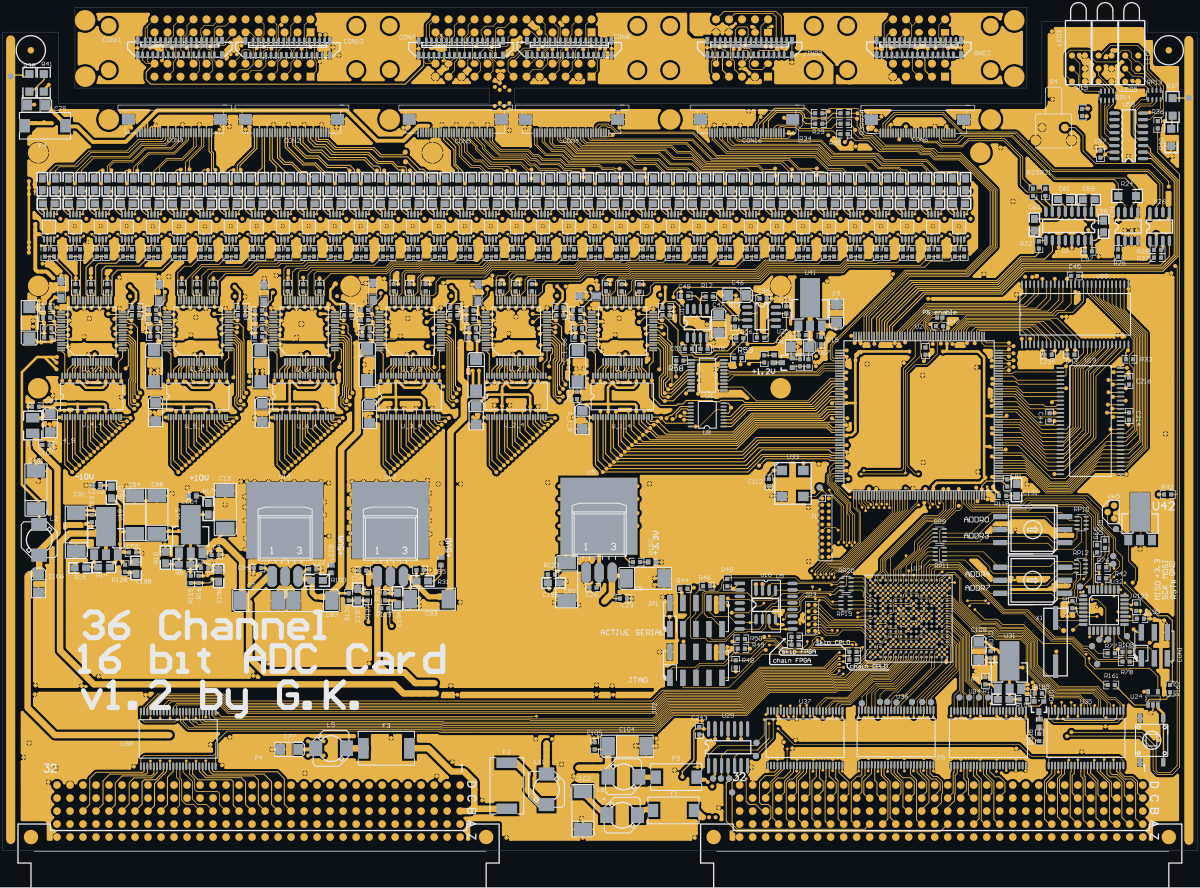
VME ADC 250K 16B 36CHA (OHWR0024 R1) is an open-hardware circuit board from the CERN Open Hardware Repository, designed in Altium Designer: a 4-layer board of 233.3 × 164.8 mm with 977 components and 1004 nets, published under CERN-OHL-1.1.
review 77% walked · 22 findings: 1 blocker · 12 major · 9 minor (238 items)
Open in the interactive viewerRead the full review
Design review
Probe recorded 22 findings: 1 blocker · 12 major · 9 minor (238 items) on this design. Each is shown here with its reasoning; the full review links every one to the pins, nets and datasheet pages it rests on.
- OpenDrainBusContentionblockerOpen
U42.1 drives '1WIRE' open-drain with no fitted pull-up (U65 is DNP)
Net '1WIRE': open-drain output U42.1 drives U32.32 and no part fitted on this board pulls its node up. U65 (to +3.3V) bridges the node to a rail and is marked not fitted (DNP): the pull-up position the design provides is empty as built. Whether the line can go high then rests on U32.32, which sits on the node with no drive on file: an output there that drives the line high makes this work as built; if none does, U42.1 can pull the line low and nothing takes it high again.
At 1WIRE
- ReferencePlaneDiscontinuitymajorOpen
'IFC_GND' crosses one void in the AGND plane on GND_PLANE at 5 places, the longest 1.13 mm (fastest: IFC_GND at 100 ps 10-90 %, ASSUMED)
Along 'IFC_GND' on TOP_LAYER, the AGND plane on GND_PLANE has 1.13 mm under the track with no copper, at (-19.86, 118.24), running to the end of the track. No single drill's anti-pad and no landing explains it: a clearance is excused only when it holds a drill and is drawn round it, or the track ends in it on the net's own pad or via, or runs through its own via's clearance and no farther. The return current detours round the void. 5 places on 1 net(s) cross it, listed below, the longest first. What cleared it: the hole at x -20.83..-12.32, y 118.11..118.36. One decision covers the void: whether these tracks may cross it, or the plane should be filled under them. No crossing has a plane on the track's other side, so the whole return meets the break.
- 'IFC_GND' on TOP_LAYER at (-19.86, 118.24), 1.13 mm over no copper, to the end of the track; other side: none: the signal layer is outermost
- 'IFC_GND' on TOP_LAYER at (-16.8, 118.24), 0.25 mm over no copper, to the end of the track; other side: none: the signal layer is outermost
- 'IFC_GND' on TOP_LAYER at (-16.86, 118.24), 0.25 mm over no copper, to the end of the track; other side: none: the signal layer is outermost
- 'IFC_GND' on TOP_LAYER at (-17.8, 118.24), 0.25 mm over no copper, to the end of the track; other side: none: the signal layer is outermost
- 'IFC_GND' on TOP_LAYER at (-17.86, 118.2), 0.17 mm over no copper, to the end of the track; other side: none: the signal layer is outermost
Every site is a row of this finding's evidence, keyed by net, layers and position. GET /api/odb/boards/27/reference-planes?group=void%3AAGND%40GND_PLANE%3Ahole%20-20.83%2C118.11%7C-12.32%2C118.36 serves each with its own layer_image region; all of them lie in x -22.08..-15.41, y 117.11..120.14 mm (board frame, Y up).
Read from the copper as drawn on the reference layer, along each track's centreline at exact breakpoints. The reference is the copper beside the track, never the layer's type or name. Whether it matters depends on each signal's edge rate, which nothing on file states for these nets: a slow static line crosses a split harmlessly, a fast edge does not.
At void:AGND@GND_PLANE:hole -20.83,118.11|-12.32,118.36
- ReferencePlaneDiscontinuitymajorOpen
129 nets change reference between +3.3V and GND at 260 vias, none with a reference that continues across (fastest: 1WIRE at 100 ps 10-90 %, ASSUMED)
At 260 via(s), on 129 net(s), the signal leaves a layer referenced by one of +3.3V and GND for a layer referenced by the other, and no plane references both layers. Different nets: no via can carry the return across; only decoupling between the two planes near the via can. The capacitor carrying the return across was measured at each via, at the knee of the crossing net's edge against 50 ohm assumed: 260 with none. 260 of them at an ASSUMED edge (no edge on file for the net): state one (net_timing_state) and it is re-read. One decision covers the pair: whether +3.3V and GND are decoupled to each other near these vias. A via whose layers have more references than these two is a site of each pair it joins. None is partial: at every one, no reference continues across the via.
- 'ANA_IN5' at (50.94, 10.15), TOP_LAYER -> BOTTOM_LAYER: GND on GND_PLANE to +3.3V on VCC_PLANE; pure, no reference continues across; stitching none, 250.2 mm of track past the via on BOTTOM_LAYER: At the 5 GHz knee of a 100 ps edge (100 ps 10-90 %, assumed: no edge is on file for the net) no capacitor carries the return; only the planes do. +3.3V and GND are not a thin pair (at most 0.2 mm), so their own capacitance does not carry the return. To serve it, change layers across the same plane, or move the signal to a layer referenced to ground. None.
- 'ANA_IN3' at (47.62, 11.88), TOP_LAYER -> BOTTOM_LAYER: GND on GND_PLANE to +3.3V on VCC_PLANE; pure, no reference continues across; stitching none, 234.6 mm of track past the via on BOTTOM_LAYER: At the 5 GHz knee of a 100 ps edge (100 ps 10-90 %, assumed: no edge is on file for the net) no capacitor carries the return; only the planes do. +3.3V and GND are not a thin pair (at most 0.2 mm), so their own capacitance does not carry the return. To serve it, change layers across the same plane, or move the signal to a layer referenced to ground. None.
- 'ANA_IN4' at (50.7, 7.93), TOP_LAYER -> BOTTOM_LAYER: GND on GND_PLANE to +3.3V on VCC_PLANE; pure, no reference continues across; stitching none, 198.2 mm of track past the via on BOTTOM_LAYER: At the 5 GHz knee of a 100 ps edge (100 ps 10-90 %, assumed: no edge is on file for the net) no capacitor carries the return; only the planes do. +3.3V and GND are not a thin pair (at most 0.2 mm), so their own capacitance does not carry the return. To serve it, change layers across the same plane, or move the signal to a layer referenced to ground. None.
- 'ANA_IN2' at (-62.7, 13.38), TOP_LAYER -> BOTTOM_LAYER: GND on GND_PLANE to +3.3V on VCC_PLANE; pure, no reference continues across; stitching none, 165.0 mm of track past the via on BOTTOM_LAYER: At the 5 GHz knee of a 100 ps edge (100 ps 10-90 %, assumed: no edge is on file for the net) no capacitor carries the return; only the planes do. +3.3V and GND are not a thin pair (at most 0.2 mm), so their own capacitance does not carry the return. To serve it, change layers across the same plane, or move the signal to a layer referenced to ground. None.
- 'ANA_IN2' at (48.92, 13.15), TOP_LAYER -> BOTTOM_LAYER: GND on GND_PLANE to +3.3V on VCC_PLANE; pure, no reference continues across; stitching none, 165.0 mm of track past the via on BOTTOM_LAYER: At the 5 GHz knee of a 100 ps edge (100 ps 10-90 %, assumed: no edge is on file for the net) no capacitor carries the return; only the planes do. +3.3V and GND are not a thin pair (at most 0.2 mm), so their own capacitance does not carry the return. To serve it, change layers across the same plane, or move the signal to a layer referenced to ground. None.
- 'DAT_DIR' at (-135.33, -12.2), TOP_LAYER -> BOTTOM_LAYER: GND on GND_PLANE to +3.3V on VCC_PLANE; pure, no reference continues across; stitching none, 131.6 mm of track past the via on BOTTOM_LAYER: At the 5 GHz knee of a 100 ps edge (100 ps 10-90 %, assumed: no edge is on file for the net) no capacitor carries the return; only the planes do. +3.3V and GND are not a thin pair (at most 0.2 mm), so their own capacitance does not carry the return. To serve it, change layers across the same plane, or move the signal to a layer referenced to ground. None.
- 'DAT_DIR' at (-127.43, -10.92), TOP_LAYER -> BOTTOM_LAYER: GND on GND_PLANE to +3.3V on VCC_PLANE; pure, no reference continues across; stitching none, 131.6 mm of track past the via on BOTTOM_LAYER: At the 5 GHz knee of a 100 ps edge (100 ps 10-90 %, assumed: no edge is on file for the net) no capacitor carries the return; only the planes do. +3.3V and GND are not a thin pair (at most 0.2 mm), so their own capacitance does not carry the return. To serve it, change layers across the same plane, or move the signal to a layer referenced to ground. None.
- 'DAT_DIR' at (-65.18, -11.56), TOP_LAYER -> BOTTOM_LAYER: GND on GND_PLANE to +3.3V on VCC_PLANE; pure, no reference continues across; stitching none, 131.6 mm of track past the via on BOTTOM_LAYER: At the 5 GHz knee of a 100 ps edge (100 ps 10-90 %, assumed: no edge is on file for the net) no capacitor carries the return; only the planes do. +3.3V and GND are not a thin pair (at most 0.2 mm), so their own capacitance does not carry the return. To serve it, change layers across the same plane, or move the signal to a layer referenced to ground. None.
- 'DAT_DIR' at (49.45, -9.47), TOP_LAYER -> BOTTOM_LAYER: GND on GND_PLANE to +3.3V on VCC_PLANE; pure, no reference continues across; stitching none, 131.6 mm of track past the via on BOTTOM_LAYER: At the 5 GHz knee of a 100 ps edge (100 ps 10-90 %, assumed: no edge is on file for the net) no capacitor carries the return; only the planes do. +3.3V and GND are not a thin pair (at most 0.2 mm), so their own capacitance does not carry the return. To serve it, change layers across the same plane, or move the signal to a layer referenced to ground. None.
- 'RECONFIG' at (-2.47, 7.83), TOP_LAYER -> BOTTOM_LAYER: GND on GND_PLANE to +3.3V on VCC_PLANE; pure, no reference continues across; stitching none, 114.9 mm of track past the via on BOTTOM_LAYER: At the 5 GHz knee of a 100 ps edge (100 ps 10-90 %, assumed: no edge is on file for the net) no capacitor carries the return; only the planes do. +3.3V and GND are not a thin pair (at most 0.2 mm), so their own capacitance does not carry the return. To serve it, change layers across the same plane, or move the signal to a layer referenced to ground. None.
- 'RECONFIG' at (39.29, -14.66), TOP_LAYER -> BOTTOM_LAYER: GND on GND_PLANE to +3.3V on VCC_PLANE; pure, no reference continues across; stitching none, 114.9 mm of track past the via on BOTTOM_LAYER: At the 5 GHz knee of a 100 ps edge (100 ps 10-90 %, assumed: no edge is on file for the net) no capacitor carries the return; only the planes do. +3.3V and GND are not a thin pair (at most 0.2 mm), so their own capacitance does not carry the return. To serve it, change layers across the same plane, or move the signal to a layer referenced to ground. None.
- 'RECONFIG' at (59.55, 76.38), TOP_LAYER -> BOTTOM_LAYER: GND on GND_PLANE to +3.3V on VCC_PLANE; pure, no reference continues across; stitching none, 114.9 mm of track past the via on BOTTOM_LAYER: At the 5 GHz knee of a 100 ps edge (100 ps 10-90 %, assumed: no edge is on file for the net) no capacitor carries the return; only the planes do. +3.3V and GND are not a thin pair (at most 0.2 mm), so their own capacitance does not carry the return. To serve it, change layers across the same plane, or move the signal to a layer referenced to ground. None.
- and 248 more
Every site is a row of this finding's evidence, keyed by net, layers and position. GET /api/odb/boards/27/reference-planes?group=refchange%3A%2B3.3V%7CGND serves each with its own layer_image region; all of them lie in x -137.33..61.55, y -17.45..108.58 mm (board frame, Y up).
The reference on each layer is the first plane the track meets leaving the via, anti-pads and the net's own copper skipped. Whether it matters depends on each signal's edge rate, which nothing on file states for these nets: a slow static line crosses a split harmlessly, a fast edge does not.
At refchange:+3.3V|GND
- CapVoltageDeratingmajorOpen
CapVoltageDerating: 52 components×52
52 checked by the review by evaluation@esharp.se — 52 different reasons
At C42, C51, C52, C88, C_10_21, C_11_21 and 46 more
Each finding, with its own headline
C42C42 sits on a 10 V rail and its voltage rating is not in the BOM
C42: on a 10 V rail but its voltage rating is not stated in the BOM — add it so the rating can be compared to the rail at all. No datasheet is on file for this part; the BOM short-spec is the source.
C51C51 sits on a 10 V rail and its voltage rating is not in the BOM
C51: on a 10 V rail but its voltage rating is not stated in the BOM — add it so the rating can be compared to the rail at all. No datasheet is on file for this part; the BOM short-spec is the source.
C52C52 sits on a 10 V rail and its voltage rating is not in the BOM
C52: on a 10 V rail but its voltage rating is not stated in the BOM — add it so the rating can be compared to the rail at all. No datasheet is on file for this part; the BOM short-spec is the source.
C88C88 sits on a 10 V rail and its voltage rating is not in the BOM
C88: on a 10 V rail but its voltage rating is not stated in the BOM — add it so the rating can be compared to the rail at all. No datasheet is on file for this part; the BOM short-spec is the source.
C_10_21C_10_21 sits on a 10 V rail and its voltage rating is not in the BOM
C_10_21: on a 10 V rail but its voltage rating is not stated in the BOM — add it so the rating can be compared to the rail at all. No datasheet is on file for this part; the BOM short-spec is the source.
C_11_21C_11_21 sits on a 10 V rail and its voltage rating is not in the BOM
C_11_21: on a 10 V rail but its voltage rating is not stated in the BOM — add it so the rating can be compared to the rail at all. No datasheet is on file for this part; the BOM short-spec is the source.
C_12_21C_12_21 sits on a 10 V rail and its voltage rating is not in the BOM
C_12_21: on a 10 V rail but its voltage rating is not stated in the BOM — add it so the rating can be compared to the rail at all. No datasheet is on file for this part; the BOM short-spec is the source.
C_13_21C_13_21 sits on a 10 V rail and its voltage rating is not in the BOM
C_13_21: on a 10 V rail but its voltage rating is not stated in the BOM — add it so the rating can be compared to the rail at all. No datasheet is on file for this part; the BOM short-spec is the source.
C_14_21C_14_21 sits on a 10 V rail and its voltage rating is not in the BOM
C_14_21: on a 10 V rail but its voltage rating is not stated in the BOM — add it so the rating can be compared to the rail at all. No datasheet is on file for this part; the BOM short-spec is the source.
C_15_21C_15_21 sits on a 10 V rail and its voltage rating is not in the BOM
C_15_21: on a 10 V rail but its voltage rating is not stated in the BOM — add it so the rating can be compared to the rail at all. No datasheet is on file for this part; the BOM short-spec is the source.
C_16_21C_16_21 sits on a 10 V rail and its voltage rating is not in the BOM
C_16_21: on a 10 V rail but its voltage rating is not stated in the BOM — add it so the rating can be compared to the rail at all. No datasheet is on file for this part; the BOM short-spec is the source.
C_17_21C_17_21 sits on a 10 V rail and its voltage rating is not in the BOM
C_17_21: on a 10 V rail but its voltage rating is not stated in the BOM — add it so the rating can be compared to the rail at all. No datasheet is on file for this part; the BOM short-spec is the source.
C_18_21C_18_21 sits on a 10 V rail and its voltage rating is not in the BOM
C_18_21: on a 10 V rail but its voltage rating is not stated in the BOM — add it so the rating can be compared to the rail at all. No datasheet is on file for this part; the BOM short-spec is the source.
C_19_21C_19_21 sits on a 10 V rail and its voltage rating is not in the BOM
C_19_21: on a 10 V rail but its voltage rating is not stated in the BOM — add it so the rating can be compared to the rail at all. No datasheet is on file for this part; the BOM short-spec is the source.
C_1_21C_1_21 sits on a 10 V rail and its voltage rating is not in the BOM
C_1_21: on a 10 V rail but its voltage rating is not stated in the BOM — add it so the rating can be compared to the rail at all. No datasheet is on file for this part; the BOM short-spec is the source.
C_1_68C_1_68 sits on a 10 V rail and its voltage rating is not in the BOM
C_1_68: on a 10 V rail but its voltage rating is not stated in the BOM — add it so the rating can be compared to the rail at all. No datasheet is on file for this part; the BOM short-spec is the source.
C_1_78C_1_78 sits on a 10 V rail and its voltage rating is not in the BOM
C_1_78: on a 10 V rail but its voltage rating is not stated in the BOM — add it so the rating can be compared to the rail at all. No datasheet is on file for this part; the BOM short-spec is the source.
C_20_21C_20_21 sits on a 10 V rail and its voltage rating is not in the BOM
C_20_21: on a 10 V rail but its voltage rating is not stated in the BOM — add it so the rating can be compared to the rail at all. No datasheet is on file for this part; the BOM short-spec is the source.
C_21_21C_21_21 sits on a 10 V rail and its voltage rating is not in the BOM
C_21_21: on a 10 V rail but its voltage rating is not stated in the BOM — add it so the rating can be compared to the rail at all. No datasheet is on file for this part; the BOM short-spec is the source.
C_22_21C_22_21 sits on a 10 V rail and its voltage rating is not in the BOM
C_22_21: on a 10 V rail but its voltage rating is not stated in the BOM — add it so the rating can be compared to the rail at all. No datasheet is on file for this part; the BOM short-spec is the source.
C_23_21C_23_21 sits on a 10 V rail and its voltage rating is not in the BOM
C_23_21: on a 10 V rail but its voltage rating is not stated in the BOM — add it so the rating can be compared to the rail at all. No datasheet is on file for this part; the BOM short-spec is the source.
C_24_21C_24_21 sits on a 10 V rail and its voltage rating is not in the BOM
C_24_21: on a 10 V rail but its voltage rating is not stated in the BOM — add it so the rating can be compared to the rail at all. No datasheet is on file for this part; the BOM short-spec is the source.
C_25_21C_25_21 sits on a 10 V rail and its voltage rating is not in the BOM
C_25_21: on a 10 V rail but its voltage rating is not stated in the BOM — add it so the rating can be compared to the rail at all. No datasheet is on file for this part; the BOM short-spec is the source.
C_26_21C_26_21 sits on a 10 V rail and its voltage rating is not in the BOM
C_26_21: on a 10 V rail but its voltage rating is not stated in the BOM — add it so the rating can be compared to the rail at all. No datasheet is on file for this part; the BOM short-spec is the source.
C_27_21C_27_21 sits on a 10 V rail and its voltage rating is not in the BOM
C_27_21: on a 10 V rail but its voltage rating is not stated in the BOM — add it so the rating can be compared to the rail at all. No datasheet is on file for this part; the BOM short-spec is the source.
C_28_21C_28_21 sits on a 10 V rail and its voltage rating is not in the BOM
C_28_21: on a 10 V rail but its voltage rating is not stated in the BOM — add it so the rating can be compared to the rail at all. No datasheet is on file for this part; the BOM short-spec is the source.
C_29_21C_29_21 sits on a 10 V rail and its voltage rating is not in the BOM
C_29_21: on a 10 V rail but its voltage rating is not stated in the BOM — add it so the rating can be compared to the rail at all. No datasheet is on file for this part; the BOM short-spec is the source.
C_2_21C_2_21 sits on a 10 V rail and its voltage rating is not in the BOM
C_2_21: on a 10 V rail but its voltage rating is not stated in the BOM — add it so the rating can be compared to the rail at all. No datasheet is on file for this part; the BOM short-spec is the source.
C_2_68C_2_68 sits on a 10 V rail and its voltage rating is not in the BOM
C_2_68: on a 10 V rail but its voltage rating is not stated in the BOM — add it so the rating can be compared to the rail at all. No datasheet is on file for this part; the BOM short-spec is the source.
C_2_78C_2_78 sits on a 10 V rail and its voltage rating is not in the BOM
C_2_78: on a 10 V rail but its voltage rating is not stated in the BOM — add it so the rating can be compared to the rail at all. No datasheet is on file for this part; the BOM short-spec is the source.
C_30_21C_30_21 sits on a 10 V rail and its voltage rating is not in the BOM
C_30_21: on a 10 V rail but its voltage rating is not stated in the BOM — add it so the rating can be compared to the rail at all. No datasheet is on file for this part; the BOM short-spec is the source.
C_31_21C_31_21 sits on a 10 V rail and its voltage rating is not in the BOM
C_31_21: on a 10 V rail but its voltage rating is not stated in the BOM — add it so the rating can be compared to the rail at all. No datasheet is on file for this part; the BOM short-spec is the source.
C_32_21C_32_21 sits on a 10 V rail and its voltage rating is not in the BOM
C_32_21: on a 10 V rail but its voltage rating is not stated in the BOM — add it so the rating can be compared to the rail at all. No datasheet is on file for this part; the BOM short-spec is the source.
C_33_21C_33_21 sits on a 10 V rail and its voltage rating is not in the BOM
C_33_21: on a 10 V rail but its voltage rating is not stated in the BOM — add it so the rating can be compared to the rail at all. No datasheet is on file for this part; the BOM short-spec is the source.
C_34_21C_34_21 sits on a 10 V rail and its voltage rating is not in the BOM
C_34_21: on a 10 V rail but its voltage rating is not stated in the BOM — add it so the rating can be compared to the rail at all. No datasheet is on file for this part; the BOM short-spec is the source.
C_35_21C_35_21 sits on a 10 V rail and its voltage rating is not in the BOM
C_35_21: on a 10 V rail but its voltage rating is not stated in the BOM — add it so the rating can be compared to the rail at all. No datasheet is on file for this part; the BOM short-spec is the source.
C_36_21C_36_21 sits on a 10 V rail and its voltage rating is not in the BOM
C_36_21: on a 10 V rail but its voltage rating is not stated in the BOM — add it so the rating can be compared to the rail at all. No datasheet is on file for this part; the BOM short-spec is the source.
C_3_21C_3_21 sits on a 10 V rail and its voltage rating is not in the BOM
C_3_21: on a 10 V rail but its voltage rating is not stated in the BOM — add it so the rating can be compared to the rail at all. No datasheet is on file for this part; the BOM short-spec is the source.
C_3_68C_3_68 sits on a 10 V rail and its voltage rating is not in the BOM
C_3_68: on a 10 V rail but its voltage rating is not stated in the BOM — add it so the rating can be compared to the rail at all. No datasheet is on file for this part; the BOM short-spec is the source.
C_3_78C_3_78 sits on a 10 V rail and its voltage rating is not in the BOM
C_3_78: on a 10 V rail but its voltage rating is not stated in the BOM — add it so the rating can be compared to the rail at all. No datasheet is on file for this part; the BOM short-spec is the source.
C_4_21C_4_21 sits on a 10 V rail and its voltage rating is not in the BOM
C_4_21: on a 10 V rail but its voltage rating is not stated in the BOM — add it so the rating can be compared to the rail at all. No datasheet is on file for this part; the BOM short-spec is the source.
C_4_68C_4_68 sits on a 10 V rail and its voltage rating is not in the BOM
C_4_68: on a 10 V rail but its voltage rating is not stated in the BOM — add it so the rating can be compared to the rail at all. No datasheet is on file for this part; the BOM short-spec is the source.
C_4_78C_4_78 sits on a 10 V rail and its voltage rating is not in the BOM
C_4_78: on a 10 V rail but its voltage rating is not stated in the BOM — add it so the rating can be compared to the rail at all. No datasheet is on file for this part; the BOM short-spec is the source.
C_5_21C_5_21 sits on a 10 V rail and its voltage rating is not in the BOM
C_5_21: on a 10 V rail but its voltage rating is not stated in the BOM — add it so the rating can be compared to the rail at all. No datasheet is on file for this part; the BOM short-spec is the source.
C_5_68C_5_68 sits on a 10 V rail and its voltage rating is not in the BOM
C_5_68: on a 10 V rail but its voltage rating is not stated in the BOM — add it so the rating can be compared to the rail at all. No datasheet is on file for this part; the BOM short-spec is the source.
C_5_78C_5_78 sits on a 10 V rail and its voltage rating is not in the BOM
C_5_78: on a 10 V rail but its voltage rating is not stated in the BOM — add it so the rating can be compared to the rail at all. No datasheet is on file for this part; the BOM short-spec is the source.
C_6_21C_6_21 sits on a 10 V rail and its voltage rating is not in the BOM
C_6_21: on a 10 V rail but its voltage rating is not stated in the BOM — add it so the rating can be compared to the rail at all. No datasheet is on file for this part; the BOM short-spec is the source.
C_6_68C_6_68 sits on a 10 V rail and its voltage rating is not in the BOM
C_6_68: on a 10 V rail but its voltage rating is not stated in the BOM — add it so the rating can be compared to the rail at all. No datasheet is on file for this part; the BOM short-spec is the source.
C_6_78C_6_78 sits on a 10 V rail and its voltage rating is not in the BOM
C_6_78: on a 10 V rail but its voltage rating is not stated in the BOM — add it so the rating can be compared to the rail at all. No datasheet is on file for this part; the BOM short-spec is the source.
C_7_21C_7_21 sits on a 10 V rail and its voltage rating is not in the BOM
C_7_21: on a 10 V rail but its voltage rating is not stated in the BOM — add it so the rating can be compared to the rail at all. No datasheet is on file for this part; the BOM short-spec is the source.
C_8_21C_8_21 sits on a 10 V rail and its voltage rating is not in the BOM
C_8_21: on a 10 V rail but its voltage rating is not stated in the BOM — add it so the rating can be compared to the rail at all. No datasheet is on file for this part; the BOM short-spec is the source.
C_9_21C_9_21 sits on a 10 V rail and its voltage rating is not in the BOM
C_9_21: on a 10 V rail but its voltage rating is not stated in the BOM — add it so the rating can be compared to the rail at all. No datasheet is on file for this part; the BOM short-spec is the source.
- CapVoltageDeratingmajorOpen
CapVoltageDerating: 54 components×54
54 checked by the review by Claude walker W2 (Cern session) — 54 different reasons
At C102, C53, C54, C55, C56, C91 and 48 more
Each finding, with its own headline
C102C102 sits on a 12 V rail and its voltage rating is not in the BOM
C102: on a 12 V rail but its voltage rating is not stated in the BOM — add it so the rating can be compared to the rail at all. No datasheet is on file for this part; the BOM short-spec is the source. '-12V' sits at -12 V; a voltage rating is a magnitude, so it is judged at 12 V.
C53C53 sits on a 12 V rail and its voltage rating is not in the BOM
C53: on a 12 V rail but its voltage rating is not stated in the BOM — add it so the rating can be compared to the rail at all. No datasheet is on file for this part; the BOM short-spec is the source. '-12V' sits at -12 V; a voltage rating is a magnitude, so it is judged at 12 V.
C54C54 sits on a 10 V rail and its voltage rating is not in the BOM
C54: on a 10 V rail but its voltage rating is not stated in the BOM — add it so the rating can be compared to the rail at all. No datasheet is on file for this part; the BOM short-spec is the source. '-10VA' sits at -10 V; a voltage rating is a magnitude, so it is judged at 10 V.
C55C55 sits on a 10 V rail and its voltage rating is not in the BOM
C55: on a 10 V rail but its voltage rating is not stated in the BOM — add it so the rating can be compared to the rail at all. No datasheet is on file for this part; the BOM short-spec is the source. '-10VA' sits at -10 V; a voltage rating is a magnitude, so it is judged at 10 V.
C56C56 sits on a 10 V rail and its voltage rating is not in the BOM
C56: on a 10 V rail but its voltage rating is not stated in the BOM — add it so the rating can be compared to the rail at all. No datasheet is on file for this part; the BOM short-spec is the source. '-10VA' sits at -10 V; a voltage rating is a magnitude, so it is judged at 10 V.
C91C91 sits on a 12 V rail and its voltage rating is not in the BOM
C91: on a 12 V rail but its voltage rating is not stated in the BOM — add it so the rating can be compared to the rail at all. No datasheet is on file for this part; the BOM short-spec is the source. '-12V' sits at -12 V; a voltage rating is a magnitude, so it is judged at 12 V.
C_10_35C_10_35 sits on a 10 V rail and its voltage rating is not in the BOM
C_10_35: on a 10 V rail but its voltage rating is not stated in the BOM — add it so the rating can be compared to the rail at all. No datasheet is on file for this part; the BOM short-spec is the source. '-10VA' sits at -10 V; a voltage rating is a magnitude, so it is judged at 10 V.
C_11_35C_11_35 sits on a 10 V rail and its voltage rating is not in the BOM
C_11_35: on a 10 V rail but its voltage rating is not stated in the BOM — add it so the rating can be compared to the rail at all. No datasheet is on file for this part; the BOM short-spec is the source. '-10VA' sits at -10 V; a voltage rating is a magnitude, so it is judged at 10 V.
C_12_35C_12_35 sits on a 10 V rail and its voltage rating is not in the BOM
C_12_35: on a 10 V rail but its voltage rating is not stated in the BOM — add it so the rating can be compared to the rail at all. No datasheet is on file for this part; the BOM short-spec is the source. '-10VA' sits at -10 V; a voltage rating is a magnitude, so it is judged at 10 V.
C_13_35C_13_35 sits on a 10 V rail and its voltage rating is not in the BOM
C_13_35: on a 10 V rail but its voltage rating is not stated in the BOM — add it so the rating can be compared to the rail at all. No datasheet is on file for this part; the BOM short-spec is the source. '-10VA' sits at -10 V; a voltage rating is a magnitude, so it is judged at 10 V.
C_14_35C_14_35 sits on a 10 V rail and its voltage rating is not in the BOM
C_14_35: on a 10 V rail but its voltage rating is not stated in the BOM — add it so the rating can be compared to the rail at all. No datasheet is on file for this part; the BOM short-spec is the source. '-10VA' sits at -10 V; a voltage rating is a magnitude, so it is judged at 10 V.
C_15_35C_15_35 sits on a 10 V rail and its voltage rating is not in the BOM
C_15_35: on a 10 V rail but its voltage rating is not stated in the BOM — add it so the rating can be compared to the rail at all. No datasheet is on file for this part; the BOM short-spec is the source. '-10VA' sits at -10 V; a voltage rating is a magnitude, so it is judged at 10 V.
C_16_35C_16_35 sits on a 10 V rail and its voltage rating is not in the BOM
C_16_35: on a 10 V rail but its voltage rating is not stated in the BOM — add it so the rating can be compared to the rail at all. No datasheet is on file for this part; the BOM short-spec is the source. '-10VA' sits at -10 V; a voltage rating is a magnitude, so it is judged at 10 V.
C_17_35C_17_35 sits on a 10 V rail and its voltage rating is not in the BOM
C_17_35: on a 10 V rail but its voltage rating is not stated in the BOM — add it so the rating can be compared to the rail at all. No datasheet is on file for this part; the BOM short-spec is the source. '-10VA' sits at -10 V; a voltage rating is a magnitude, so it is judged at 10 V.
C_18_35C_18_35 sits on a 10 V rail and its voltage rating is not in the BOM
C_18_35: on a 10 V rail but its voltage rating is not stated in the BOM — add it so the rating can be compared to the rail at all. No datasheet is on file for this part; the BOM short-spec is the source. '-10VA' sits at -10 V; a voltage rating is a magnitude, so it is judged at 10 V.
C_19_35C_19_35 sits on a 10 V rail and its voltage rating is not in the BOM
C_19_35: on a 10 V rail but its voltage rating is not stated in the BOM — add it so the rating can be compared to the rail at all. No datasheet is on file for this part; the BOM short-spec is the source. '-10VA' sits at -10 V; a voltage rating is a magnitude, so it is judged at 10 V.
C_1_35C_1_35 sits on a 10 V rail and its voltage rating is not in the BOM
C_1_35: on a 10 V rail but its voltage rating is not stated in the BOM — add it so the rating can be compared to the rail at all. No datasheet is on file for this part; the BOM short-spec is the source. '-10VA' sits at -10 V; a voltage rating is a magnitude, so it is judged at 10 V.
C_1_69C_1_69 sits on a 10 V rail and its voltage rating is not in the BOM
C_1_69: on a 10 V rail but its voltage rating is not stated in the BOM — add it so the rating can be compared to the rail at all. No datasheet is on file for this part; the BOM short-spec is the source. '-10VA' sits at -10 V; a voltage rating is a magnitude, so it is judged at 10 V.
C_1_79C_1_79 sits on a 10 V rail and its voltage rating is not in the BOM
C_1_79: on a 10 V rail but its voltage rating is not stated in the BOM — add it so the rating can be compared to the rail at all. No datasheet is on file for this part; the BOM short-spec is the source. '-10VA' sits at -10 V; a voltage rating is a magnitude, so it is judged at 10 V.
C_20_35C_20_35 sits on a 10 V rail and its voltage rating is not in the BOM
C_20_35: on a 10 V rail but its voltage rating is not stated in the BOM — add it so the rating can be compared to the rail at all. No datasheet is on file for this part; the BOM short-spec is the source. '-10VA' sits at -10 V; a voltage rating is a magnitude, so it is judged at 10 V.
C_21_35C_21_35 sits on a 10 V rail and its voltage rating is not in the BOM
C_21_35: on a 10 V rail but its voltage rating is not stated in the BOM — add it so the rating can be compared to the rail at all. No datasheet is on file for this part; the BOM short-spec is the source. '-10VA' sits at -10 V; a voltage rating is a magnitude, so it is judged at 10 V.
C_22_35C_22_35 sits on a 10 V rail and its voltage rating is not in the BOM
C_22_35: on a 10 V rail but its voltage rating is not stated in the BOM — add it so the rating can be compared to the rail at all. No datasheet is on file for this part; the BOM short-spec is the source. '-10VA' sits at -10 V; a voltage rating is a magnitude, so it is judged at 10 V.
C_23_35C_23_35 sits on a 10 V rail and its voltage rating is not in the BOM
C_23_35: on a 10 V rail but its voltage rating is not stated in the BOM — add it so the rating can be compared to the rail at all. No datasheet is on file for this part; the BOM short-spec is the source. '-10VA' sits at -10 V; a voltage rating is a magnitude, so it is judged at 10 V.
C_24_35C_24_35 sits on a 10 V rail and its voltage rating is not in the BOM
C_24_35: on a 10 V rail but its voltage rating is not stated in the BOM — add it so the rating can be compared to the rail at all. No datasheet is on file for this part; the BOM short-spec is the source. '-10VA' sits at -10 V; a voltage rating is a magnitude, so it is judged at 10 V.
C_25_35C_25_35 sits on a 10 V rail and its voltage rating is not in the BOM
C_25_35: on a 10 V rail but its voltage rating is not stated in the BOM — add it so the rating can be compared to the rail at all. No datasheet is on file for this part; the BOM short-spec is the source. '-10VA' sits at -10 V; a voltage rating is a magnitude, so it is judged at 10 V.
C_26_35C_26_35 sits on a 10 V rail and its voltage rating is not in the BOM
C_26_35: on a 10 V rail but its voltage rating is not stated in the BOM — add it so the rating can be compared to the rail at all. No datasheet is on file for this part; the BOM short-spec is the source. '-10VA' sits at -10 V; a voltage rating is a magnitude, so it is judged at 10 V.
C_27_35C_27_35 sits on a 10 V rail and its voltage rating is not in the BOM
C_27_35: on a 10 V rail but its voltage rating is not stated in the BOM — add it so the rating can be compared to the rail at all. No datasheet is on file for this part; the BOM short-spec is the source. '-10VA' sits at -10 V; a voltage rating is a magnitude, so it is judged at 10 V.
C_28_35C_28_35 sits on a 10 V rail and its voltage rating is not in the BOM
C_28_35: on a 10 V rail but its voltage rating is not stated in the BOM — add it so the rating can be compared to the rail at all. No datasheet is on file for this part; the BOM short-spec is the source. '-10VA' sits at -10 V; a voltage rating is a magnitude, so it is judged at 10 V.
C_29_35C_29_35 sits on a 10 V rail and its voltage rating is not in the BOM
C_29_35: on a 10 V rail but its voltage rating is not stated in the BOM — add it so the rating can be compared to the rail at all. No datasheet is on file for this part; the BOM short-spec is the source. '-10VA' sits at -10 V; a voltage rating is a magnitude, so it is judged at 10 V.
C_2_35C_2_35 sits on a 10 V rail and its voltage rating is not in the BOM
C_2_35: on a 10 V rail but its voltage rating is not stated in the BOM — add it so the rating can be compared to the rail at all. No datasheet is on file for this part; the BOM short-spec is the source. '-10VA' sits at -10 V; a voltage rating is a magnitude, so it is judged at 10 V.
C_2_69C_2_69 sits on a 10 V rail and its voltage rating is not in the BOM
C_2_69: on a 10 V rail but its voltage rating is not stated in the BOM — add it so the rating can be compared to the rail at all. No datasheet is on file for this part; the BOM short-spec is the source. '-10VA' sits at -10 V; a voltage rating is a magnitude, so it is judged at 10 V.
C_2_79C_2_79 sits on a 10 V rail and its voltage rating is not in the BOM
C_2_79: on a 10 V rail but its voltage rating is not stated in the BOM — add it so the rating can be compared to the rail at all. No datasheet is on file for this part; the BOM short-spec is the source. '-10VA' sits at -10 V; a voltage rating is a magnitude, so it is judged at 10 V.
C_30_35C_30_35 sits on a 10 V rail and its voltage rating is not in the BOM
C_30_35: on a 10 V rail but its voltage rating is not stated in the BOM — add it so the rating can be compared to the rail at all. No datasheet is on file for this part; the BOM short-spec is the source. '-10VA' sits at -10 V; a voltage rating is a magnitude, so it is judged at 10 V.
C_31_35C_31_35 sits on a 10 V rail and its voltage rating is not in the BOM
C_31_35: on a 10 V rail but its voltage rating is not stated in the BOM — add it so the rating can be compared to the rail at all. No datasheet is on file for this part; the BOM short-spec is the source. '-10VA' sits at -10 V; a voltage rating is a magnitude, so it is judged at 10 V.
C_32_35C_32_35 sits on a 10 V rail and its voltage rating is not in the BOM
C_32_35: on a 10 V rail but its voltage rating is not stated in the BOM — add it so the rating can be compared to the rail at all. No datasheet is on file for this part; the BOM short-spec is the source. '-10VA' sits at -10 V; a voltage rating is a magnitude, so it is judged at 10 V.
C_33_35C_33_35 sits on a 10 V rail and its voltage rating is not in the BOM
C_33_35: on a 10 V rail but its voltage rating is not stated in the BOM — add it so the rating can be compared to the rail at all. No datasheet is on file for this part; the BOM short-spec is the source. '-10VA' sits at -10 V; a voltage rating is a magnitude, so it is judged at 10 V.
C_34_35C_34_35 sits on a 10 V rail and its voltage rating is not in the BOM
C_34_35: on a 10 V rail but its voltage rating is not stated in the BOM — add it so the rating can be compared to the rail at all. No datasheet is on file for this part; the BOM short-spec is the source. '-10VA' sits at -10 V; a voltage rating is a magnitude, so it is judged at 10 V.
C_35_35C_35_35 sits on a 10 V rail and its voltage rating is not in the BOM
C_35_35: on a 10 V rail but its voltage rating is not stated in the BOM — add it so the rating can be compared to the rail at all. No datasheet is on file for this part; the BOM short-spec is the source. '-10VA' sits at -10 V; a voltage rating is a magnitude, so it is judged at 10 V.
C_36_35C_36_35 sits on a 10 V rail and its voltage rating is not in the BOM
C_36_35: on a 10 V rail but its voltage rating is not stated in the BOM — add it so the rating can be compared to the rail at all. No datasheet is on file for this part; the BOM short-spec is the source. '-10VA' sits at -10 V; a voltage rating is a magnitude, so it is judged at 10 V.
C_3_35C_3_35 sits on a 10 V rail and its voltage rating is not in the BOM
C_3_35: on a 10 V rail but its voltage rating is not stated in the BOM — add it so the rating can be compared to the rail at all. No datasheet is on file for this part; the BOM short-spec is the source. '-10VA' sits at -10 V; a voltage rating is a magnitude, so it is judged at 10 V.
C_3_69C_3_69 sits on a 10 V rail and its voltage rating is not in the BOM
C_3_69: on a 10 V rail but its voltage rating is not stated in the BOM — add it so the rating can be compared to the rail at all. No datasheet is on file for this part; the BOM short-spec is the source. '-10VA' sits at -10 V; a voltage rating is a magnitude, so it is judged at 10 V.
C_3_79C_3_79 sits on a 10 V rail and its voltage rating is not in the BOM
C_3_79: on a 10 V rail but its voltage rating is not stated in the BOM — add it so the rating can be compared to the rail at all. No datasheet is on file for this part; the BOM short-spec is the source. '-10VA' sits at -10 V; a voltage rating is a magnitude, so it is judged at 10 V.
C_4_35C_4_35 sits on a 10 V rail and its voltage rating is not in the BOM
C_4_35: on a 10 V rail but its voltage rating is not stated in the BOM — add it so the rating can be compared to the rail at all. No datasheet is on file for this part; the BOM short-spec is the source. '-10VA' sits at -10 V; a voltage rating is a magnitude, so it is judged at 10 V.
C_4_69C_4_69 sits on a 10 V rail and its voltage rating is not in the BOM
C_4_69: on a 10 V rail but its voltage rating is not stated in the BOM — add it so the rating can be compared to the rail at all. No datasheet is on file for this part; the BOM short-spec is the source. '-10VA' sits at -10 V; a voltage rating is a magnitude, so it is judged at 10 V.
C_4_79C_4_79 sits on a 10 V rail and its voltage rating is not in the BOM
C_4_79: on a 10 V rail but its voltage rating is not stated in the BOM — add it so the rating can be compared to the rail at all. No datasheet is on file for this part; the BOM short-spec is the source. '-10VA' sits at -10 V; a voltage rating is a magnitude, so it is judged at 10 V.
C_5_35C_5_35 sits on a 10 V rail and its voltage rating is not in the BOM
C_5_35: on a 10 V rail but its voltage rating is not stated in the BOM — add it so the rating can be compared to the rail at all. No datasheet is on file for this part; the BOM short-spec is the source. '-10VA' sits at -10 V; a voltage rating is a magnitude, so it is judged at 10 V.
C_5_69C_5_69 sits on a 10 V rail and its voltage rating is not in the BOM
C_5_69: on a 10 V rail but its voltage rating is not stated in the BOM — add it so the rating can be compared to the rail at all. No datasheet is on file for this part; the BOM short-spec is the source. '-10VA' sits at -10 V; a voltage rating is a magnitude, so it is judged at 10 V.
C_5_79C_5_79 sits on a 10 V rail and its voltage rating is not in the BOM
C_5_79: on a 10 V rail but its voltage rating is not stated in the BOM — add it so the rating can be compared to the rail at all. No datasheet is on file for this part; the BOM short-spec is the source. '-10VA' sits at -10 V; a voltage rating is a magnitude, so it is judged at 10 V.
C_6_35C_6_35 sits on a 10 V rail and its voltage rating is not in the BOM
C_6_35: on a 10 V rail but its voltage rating is not stated in the BOM — add it so the rating can be compared to the rail at all. No datasheet is on file for this part; the BOM short-spec is the source. '-10VA' sits at -10 V; a voltage rating is a magnitude, so it is judged at 10 V.
C_6_69C_6_69 sits on a 10 V rail and its voltage rating is not in the BOM
C_6_69: on a 10 V rail but its voltage rating is not stated in the BOM — add it so the rating can be compared to the rail at all. No datasheet is on file for this part; the BOM short-spec is the source. '-10VA' sits at -10 V; a voltage rating is a magnitude, so it is judged at 10 V.
C_6_79C_6_79 sits on a 10 V rail and its voltage rating is not in the BOM
C_6_79: on a 10 V rail but its voltage rating is not stated in the BOM — add it so the rating can be compared to the rail at all. No datasheet is on file for this part; the BOM short-spec is the source. '-10VA' sits at -10 V; a voltage rating is a magnitude, so it is judged at 10 V.
C_7_35C_7_35 sits on a 10 V rail and its voltage rating is not in the BOM
C_7_35: on a 10 V rail but its voltage rating is not stated in the BOM — add it so the rating can be compared to the rail at all. No datasheet is on file for this part; the BOM short-spec is the source. '-10VA' sits at -10 V; a voltage rating is a magnitude, so it is judged at 10 V.
C_8_35C_8_35 sits on a 10 V rail and its voltage rating is not in the BOM
C_8_35: on a 10 V rail but its voltage rating is not stated in the BOM — add it so the rating can be compared to the rail at all. No datasheet is on file for this part; the BOM short-spec is the source. '-10VA' sits at -10 V; a voltage rating is a magnitude, so it is judged at 10 V.
C_9_35C_9_35 sits on a 10 V rail and its voltage rating is not in the BOM
C_9_35: on a 10 V rail but its voltage rating is not stated in the BOM — add it so the rating can be compared to the rail at all. No datasheet is on file for this part; the BOM short-spec is the source. '-10VA' sits at -10 V; a voltage rating is a magnitude, so it is judged at 10 V.
- CapVoltageDeratingmajorOpen
CapVoltageDerating: 7 components×7
7 checked by the review by Claude walker W4 (Cern session) — 7 different reasons
At C104, C105, C13, C18, C3, C7, C94
Each finding, with its own headline
C104C104 sits on a 12 V rail and its voltage rating is not in the BOM
C104: on a 12 V rail but its voltage rating is not stated in the BOM — add it so the rating can be compared to the rail at all. No datasheet is on file for this part; the BOM short-spec is the source.
C105C105 sits on a 12 V rail and its voltage rating is not in the BOM
C105: on a 12 V rail but its voltage rating is not stated in the BOM — add it so the rating can be compared to the rail at all. No datasheet is on file for this part; the BOM short-spec is the source.
C13C13 sits on a 12 V rail and its voltage rating is not in the BOM
C13: on a 12 V rail but its voltage rating is not stated in the BOM — add it so the rating can be compared to the rail at all. No datasheet is on file for this part; the BOM short-spec is the source.
C18C18 sits on a 12 V rail and its voltage rating is not in the BOM
C18: on a 12 V rail but its voltage rating is not stated in the BOM — add it so the rating can be compared to the rail at all. No datasheet is on file for this part; the BOM short-spec is the source.
C3C3 sits on a 12 V rail and its voltage rating is not in the BOM
C3: on a 12 V rail but its voltage rating is not stated in the BOM — add it so the rating can be compared to the rail at all. No datasheet is on file for this part; the BOM short-spec is the source.
C7C7 sits on a 12 V rail and its voltage rating is not in the BOM
C7: on a 12 V rail but its voltage rating is not stated in the BOM — add it so the rating can be compared to the rail at all. No datasheet is on file for this part; the BOM short-spec is the source.
C94C94 sits on a 12 V rail and its voltage rating is not in the BOM
C94: on a 12 V rail but its voltage rating is not stated in the BOM — add it so the rating can be compared to the rail at all. No datasheet is on file for this part; the BOM short-spec is the source.
- DecapViaFanoutmajorOpen
DecapViaFanout: 67 components×67
67 checked by the review by Claude walker W4 (Cern session) — 67 different reasons
At C101, C109, C112, C54, C77, C8 and 61 more
Each finding, with its own headline
C101C101 on '+3.3VD': its ground pad over 2.15 mm, adding about 0.93 nH to its loop, past Probe's 0.5 nH starting value; put the vias at the pads
C101 on '+3.3VD': its ground pad over 2.15 mm, adding about 0.93 nH to its loop, past Probe's 0.5 nH starting value; put the vias at the pads. C101.1 (rail) not measured: its tracks reach no via within 6 mm; C101.2 (ground) runs 2.15 mm along its copper to its nearest via, 1.15 mm past the 1 mm beside the pad: 0.93 nH. Each run past the pad as one conductor of a pair 7.37 mm apart (the pad pitch), 0.2 l ln(D/R) nH with R 0.127 mm (the track's width is not read): 0.93 nH in all. Put the vias at the pads (or in them), one per pad at least, the rail's and the ground's close together; the capacitor's own inductance as mounted is 1.58 nH (pad 0.20 nH + no via of the first net within 1 mm of its pad: the study's 0.6 nH per mm of 0.64 mm depth, ASSUMED). 0.5 nH is Probe's starting value, about the whole mounted inductance of a well-mounted 0402.
C109C109 on '+1.8V': its rail pad reaches its via over 4.89 mm of track and its ground pad over 2.45 mm, adding about 3.56 nH to its loop, past Probe's 0.5 nH starting value; put the vias at the pads
C109 on '+1.8V': its rail pad reaches its via over 4.89 mm of track and its ground pad over 2.45 mm, adding about 3.56 nH to its loop, past Probe's 0.5 nH starting value; put the vias at the pads. C109.1 (rail) runs 4.89 mm along its copper to its nearest via, 3.89 mm past the 1 mm beside the pad: 2.59 nH; C109.2 (ground) runs 2.45 mm along its copper to its nearest via, 1.45 mm past the 1 mm beside the pad: 0.97 nH. Each run past the pad as one conductor of a pair 3.56 mm apart (the pad pitch), 0.2 l ln(D/R) nH with R 0.127 mm (the track's width is not read): 3.56 nH in all. Put the vias at the pads (or in them), one per pad at least, the rail's and the ground's close together; the capacitor's own inductance as mounted is 1.38 nH (pad 0.20 nH + no via of the first net within 1 mm of its pad: the study's 0.6 nH per mm of 0.64 mm depth, ASSUMED). 0.5 nH is Probe's starting value, about the whole mounted inductance of a well-mounted 0402.
C112C112 on '+3.3V': its rail pad reaches its via over 2.04 mm of track and its ground pad over 2.13 mm, adding about 1.04 nH to its loop, past Probe's 0.5 nH starting value; put the vias at the pads
C112 on '+3.3V': its rail pad reaches its via over 2.04 mm of track and its ground pad over 2.13 mm, adding about 1.04 nH to its loop, past Probe's 0.5 nH starting value; put the vias at the pads. C112.2 (rail) runs 2.04 mm along its copper to its nearest via, 1.04 mm past the 1 mm beside the pad: 0.50 nH; C112.1 (ground) runs 2.13 mm along its copper to its nearest via, 1.13 mm past the 1 mm beside the pad: 0.54 nH. Each run past the pad as one conductor of a pair 1.40 mm apart (the pad pitch), 0.2 l ln(D/R) nH with R 0.127 mm (the track's width is not read): 1.04 nH in all. Put the vias at the pads (or in them), one per pad at least, the rail's and the ground's close together; the capacitor's own inductance as mounted is 0.99 nH (pad 0.10 nH + no via of the first net within 1 mm of its pad: the study's 0.6 nH per mm of 0.64 mm depth, ASSUMED). 0.5 nH is Probe's starting value, about the whole mounted inductance of a well-mounted 0402.
C54C54 on '-10VA': its rail pad reaches its via over 5.59 mm of track and its ground pad over 2.44 mm, adding about 4.90 nH to its loop, past Probe's 0.5 nH starting value; put the vias at the pads
C54 on '-10VA': its rail pad reaches its via over 5.59 mm of track and its ground pad over 2.44 mm, adding about 4.90 nH to its loop, past Probe's 0.5 nH starting value; put the vias at the pads. C54.2 (rail) runs 5.59 mm along its copper to its nearest via, 4.59 mm past the 1 mm beside the pad: 3.73 nH; C54.1 (ground) runs 2.44 mm along its copper to its nearest via, 1.44 mm past the 1 mm beside the pad: 1.17 nH. Each run past the pad as one conductor of a pair 7.37 mm apart (the pad pitch), 0.2 l ln(D/R) nH with R 0.127 mm (the track's width is not read): 4.90 nH in all. Put the vias at the pads (or in them), one per pad at least, the rail's and the ground's close together; the capacitor's own inductance as mounted is 1.58 nH (pad 0.20 nH + no via of the first net within 1 mm of its pad: the study's 0.6 nH per mm of 0.64 mm depth, ASSUMED). 0.5 nH is Probe's starting value, about the whole mounted inductance of a well-mounted 0402.
C77C77 on '+5V': its rail pad reaches its via over 3.42 mm of track and its ground pad over 1.65 mm, adding about 2.05 nH to its loop, past Probe's 0.5 nH starting value; put the vias at the pads
C77 on '+5V': its rail pad reaches its via over 3.42 mm of track and its ground pad over 1.65 mm, adding about 2.05 nH to its loop, past Probe's 0.5 nH starting value; put the vias at the pads. C77.1 (rail) runs 3.42 mm along its copper to its nearest via, 2.42 mm past the 1 mm beside the pad: 1.61 nH; C77.2 (ground) runs 1.65 mm along its copper to its nearest via, 0.65 mm past the 1 mm beside the pad: 0.43 nH. Each run past the pad as one conductor of a pair 3.56 mm apart (the pad pitch), 0.2 l ln(D/R) nH with R 0.127 mm (the track's width is not read): 2.05 nH in all. Put the vias at the pads (or in them), one per pad at least, the rail's and the ground's close together; the capacitor's own inductance as mounted is 1.38 nH (pad 0.20 nH + no via of the first net within 1 mm of its pad: the study's 0.6 nH per mm of 0.64 mm depth, ASSUMED). 0.5 nH is Probe's starting value, about the whole mounted inductance of a well-mounted 0402.
C8C8 on 'NetC8_1': its rail pad reaches its via over 0.00 mm of track and its ground pad over 1.91 mm, adding about 0.74 nH to its loop, past Probe's 0.5 nH starting value; put the vias at the pads
C8 on 'NetC8_1': its rail pad reaches its via over 0.00 mm of track and its ground pad over 1.91 mm, adding about 0.74 nH to its loop, past Probe's 0.5 nH starting value; put the vias at the pads. C8.1 (rail) runs 0.00 mm along its copper to its nearest via, beside the pad; C8.2 (ground) runs 1.91 mm along its copper to its nearest via, 0.91 mm past the 1 mm beside the pad: 0.74 nH. Each run past the pad as one conductor of a pair 7.37 mm apart (the pad pitch), 0.2 l ln(D/R) nH with R 0.127 mm (the track's width is not read): 0.74 nH in all. Put the vias at the pads (or in them), one per pad at least, the rail's and the ground's close together; the capacitor's own inductance as mounted is 1.58 nH (pad 0.20 nH + no via of the first net within 1 mm of its pad: the study's 0.6 nH per mm of 0.64 mm depth, ASSUMED). 0.5 nH is Probe's starting value, about the whole mounted inductance of a well-mounted 0402.
C84C84 on '+3.3VBUF': its ground pad over 5.90 mm, adding about 2.35 nH to its loop, past Probe's 0.5 nH starting value; put the vias at the pads
C84 on '+3.3VBUF': its ground pad over 5.90 mm, adding about 2.35 nH to its loop, past Probe's 0.5 nH starting value; put the vias at the pads. C84.1 (rail) not measured: its tracks reach no via within 6 mm; C84.2 (ground) runs 5.90 mm along its copper to its nearest via, 4.90 mm past the 1 mm beside the pad: 2.35 nH. Each run past the pad as one conductor of a pair 1.40 mm apart (the pad pitch), 0.2 l ln(D/R) nH with R 0.127 mm (the track's width is not read): 2.35 nH in all. Put the vias at the pads (or in them), one per pad at least, the rail's and the ground's close together; the capacitor's own inductance as mounted is 0.99 nH (pad 0.10 nH + no via of the first net within 1 mm of its pad: the study's 0.6 nH per mm of 0.64 mm depth, ASSUMED). 0.5 nH is Probe's starting value, about the whole mounted inductance of a well-mounted 0402.
C88C88 on '+10VA': its rail pad reaches its via over 2.65 mm of track and its ground pad over 0.00 mm, adding about 1.34 nH to its loop, past Probe's 0.5 nH starting value; put the vias at the pads
C88 on '+10VA': its rail pad reaches its via over 2.65 mm of track and its ground pad over 0.00 mm, adding about 1.34 nH to its loop, past Probe's 0.5 nH starting value; put the vias at the pads. C88.1 (rail) runs 2.65 mm along its copper to its nearest via, 1.65 mm past the 1 mm beside the pad: 1.34 nH; C88.2 (ground) runs 0.00 mm along its copper to its nearest via, beside the pad. Each run past the pad as one conductor of a pair 7.37 mm apart (the pad pitch), 0.2 l ln(D/R) nH with R 0.127 mm (the track's width is not read): 1.34 nH in all. Put the vias at the pads (or in them), one per pad at least, the rail's and the ground's close together; the capacitor's own inductance as mounted is 1.58 nH (pad 0.20 nH + no via of the first net within 1 mm of its pad: the study's 0.6 nH per mm of 0.64 mm depth, ASSUMED). 0.5 nH is Probe's starting value, about the whole mounted inductance of a well-mounted 0402.
C93C93 on '+5VD': its rail pad reaches its via over 3.59 mm of track and its ground pad over 1.77 mm, adding about 2.73 nH to its loop, past Probe's 0.5 nH starting value; put the vias at the pads
C93 on '+5VD': its rail pad reaches its via over 3.59 mm of track and its ground pad over 1.77 mm, adding about 2.73 nH to its loop, past Probe's 0.5 nH starting value; put the vias at the pads. C93.2 (rail) runs 3.59 mm along its copper to its nearest via, 2.59 mm past the 1 mm beside the pad: 2.10 nH; C93.1 (ground) runs 1.77 mm along its copper to its nearest via, 0.77 mm past the 1 mm beside the pad: 0.63 nH. Each run past the pad as one conductor of a pair 7.37 mm apart (the pad pitch), 0.2 l ln(D/R) nH with R 0.127 mm (the track's width is not read): 2.73 nH in all. Put the vias at the pads (or in them), one per pad at least, the rail's and the ground's close together; the capacitor's own inductance as mounted is 1.58 nH (pad 0.20 nH + no via of the first net within 1 mm of its pad: the study's 0.6 nH per mm of 0.64 mm depth, ASSUMED). 0.5 nH is Probe's starting value, about the whole mounted inductance of a well-mounted 0402.
C95C95 on '+5VD': its rail pad reaches its via over 3.61 mm of track and its ground pad over 1.27 mm, adding about 1.38 nH to its loop, past Probe's 0.5 nH starting value; put the vias at the pads
C95 on '+5VD': its rail pad reaches its via over 3.61 mm of track and its ground pad over 1.27 mm, adding about 1.38 nH to its loop, past Probe's 0.5 nH starting value; put the vias at the pads. C95.1 (rail) runs 3.61 mm along its copper to its nearest via, 2.61 mm past the 1 mm beside the pad: 1.25 nH; C95.2 (ground) runs 1.27 mm along its copper to its nearest via, 0.27 mm past the 1 mm beside the pad: 0.13 nH. Each run past the pad as one conductor of a pair 1.40 mm apart (the pad pitch), 0.2 l ln(D/R) nH with R 0.127 mm (the track's width is not read): 1.38 nH in all. Put the vias at the pads (or in them), one per pad at least, the rail's and the ground's close together; the capacitor's own inductance as mounted is 0.99 nH (pad 0.10 nH + no via of the first net within 1 mm of its pad: the study's 0.6 nH per mm of 0.64 mm depth, ASSUMED). 0.5 nH is Probe's starting value, about the whole mounted inductance of a well-mounted 0402.
C_1_1C_1_1 on '+3.3VD': its rail pad reaches its via over 1.96 mm of track and its ground pad over 1.93 mm, adding about 1.26 nH to its loop, past Probe's 0.5 nH starting value; put the vias at the pads
C_1_1 on '+3.3VD': its rail pad reaches its via over 1.96 mm of track and its ground pad over 1.93 mm, adding about 1.26 nH to its loop, past Probe's 0.5 nH starting value; put the vias at the pads. C_1_1.1 (rail) runs 1.96 mm along its copper to its nearest via, 0.96 mm past the 1 mm beside the pad: 0.64 nH; C_1_1.2 (ground) runs 1.93 mm along its copper to its nearest via, 0.93 mm past the 1 mm beside the pad: 0.62 nH. Each run past the pad as one conductor of a pair 3.56 mm apart (the pad pitch), 0.2 l ln(D/R) nH with R 0.127 mm (the track's width is not read): 1.26 nH in all. Put the vias at the pads (or in them), one per pad at least, the rail's and the ground's close together; the capacitor's own inductance as mounted is 1.38 nH (pad 0.20 nH + no via of the first net within 1 mm of its pad: the study's 0.6 nH per mm of 0.64 mm depth, ASSUMED). 0.5 nH is Probe's starting value, about the whole mounted inductance of a well-mounted 0402.
C_1_2C_1_2 on '+5VD': its rail pad reaches its via over 3.45 mm of track and its ground pad over 2.15 mm, adding about 2.40 nH to its loop, past Probe's 0.5 nH starting value; put the vias at the pads
C_1_2 on '+5VD': its rail pad reaches its via over 3.45 mm of track and its ground pad over 2.15 mm, adding about 2.40 nH to its loop, past Probe's 0.5 nH starting value; put the vias at the pads. C_1_2.1 (rail) runs 3.45 mm along its copper to its nearest via, 2.45 mm past the 1 mm beside the pad: 1.63 nH; C_1_2.2 (ground) runs 2.15 mm along its copper to its nearest via, 1.15 mm past the 1 mm beside the pad: 0.77 nH. Each run past the pad as one conductor of a pair 3.56 mm apart (the pad pitch), 0.2 l ln(D/R) nH with R 0.127 mm (the track's width is not read): 2.40 nH in all. Put the vias at the pads (or in them), one per pad at least, the rail's and the ground's close together; the capacitor's own inductance as mounted is 1.38 nH (pad 0.20 nH + no via of the first net within 1 mm of its pad: the study's 0.6 nH per mm of 0.64 mm depth, ASSUMED). 0.5 nH is Probe's starting value, about the whole mounted inductance of a well-mounted 0402.
C_1_64C_1_64 on '+5VA': its ground pad over 3.37 mm, adding about 1.83 nH to its loop, past Probe's 0.5 nH starting value; put the vias at the pads
C_1_64 on '+5VA': its ground pad over 3.37 mm, adding about 1.83 nH to its loop, past Probe's 0.5 nH starting value; put the vias at the pads. C_1_64.1 (rail) not measured: its own track joins it to U_1_3.46 (0.00 mm) before any via: it serves that pin directly, and its loop does not run through its vias; C_1_64.2 (ground) runs 3.37 mm along its copper to its nearest via, 2.37 mm past the 1 mm beside the pad: 1.83 nH. Each run past the pad as one conductor of a pair 6.10 mm apart (the pad pitch), 0.2 l ln(D/R) nH with R 0.127 mm (the track's width is not read): 1.83 nH in all. Put the vias at the pads (or in them), one per pad at least, the rail's and the ground's close together; the capacitor's own inductance as mounted is 1.58 nH (pad 0.20 nH + no via of the first net within 1 mm of its pad: the study's 0.6 nH per mm of 0.64 mm depth, ASSUMED). 0.5 nH is Probe's starting value, about the whole mounted inductance of a well-mounted 0402.
C_1_65C_1_65 on '+5VA': its rail pad reaches its via over 0.00 mm of track and its ground pad over 3.81 mm, adding about 2.18 nH to its loop, past Probe's 0.5 nH starting value; put the vias at the pads
C_1_65 on '+5VA': its rail pad reaches its via over 0.00 mm of track and its ground pad over 3.81 mm, adding about 2.18 nH to its loop, past Probe's 0.5 nH starting value; put the vias at the pads. C_1_65.1 (rail) runs 0.00 mm along its copper to its nearest via, beside the pad; C_1_65.2 (ground) runs 3.81 mm along its copper to its nearest via, 2.81 mm past the 1 mm beside the pad: 2.18 nH. Each run past the pad as one conductor of a pair 6.10 mm apart (the pad pitch), 0.2 l ln(D/R) nH with R 0.127 mm (the track's width is not read): 2.18 nH in all. Put the vias at the pads (or in them), one per pad at least, the rail's and the ground's close together; the capacitor's own inductance as mounted is 1.58 nH (pad 0.20 nH + no via of the first net within 1 mm of its pad: the study's 0.6 nH per mm of 0.64 mm depth, ASSUMED). 0.5 nH is Probe's starting value, about the whole mounted inductance of a well-mounted 0402.
C_1_66C_1_66 on '+5VA': its rail pad reaches its via over 2.28 mm of track and its ground pad over 2.63 mm, adding about 2.25 nH to its loop, past Probe's 0.5 nH starting value; put the vias at the pads
C_1_66 on '+5VA': its rail pad reaches its via over 2.28 mm of track and its ground pad over 2.63 mm, adding about 2.25 nH to its loop, past Probe's 0.5 nH starting value; put the vias at the pads. C_1_66.1 (rail) runs 2.28 mm along its copper to its nearest via, 1.28 mm past the 1 mm beside the pad: 0.99 nH; C_1_66.2 (ground) runs 2.63 mm along its copper to its nearest via, 1.63 mm past the 1 mm beside the pad: 1.26 nH. Each run past the pad as one conductor of a pair 6.10 mm apart (the pad pitch), 0.2 l ln(D/R) nH with R 0.127 mm (the track's width is not read): 2.25 nH in all. Put the vias at the pads (or in them), one per pad at least, the rail's and the ground's close together; the capacitor's own inductance as mounted is 1.58 nH (pad 0.20 nH + no via of the first net within 1 mm of its pad: the study's 0.6 nH per mm of 0.64 mm depth, ASSUMED). 0.5 nH is Probe's starting value, about the whole mounted inductance of a well-mounted 0402.
C_1_67C_1_67 on '+5VA': its rail pad reaches its via over 0.00 mm of track and its ground pad over 3.75 mm, adding about 2.13 nH to its loop, past Probe's 0.5 nH starting value; put the vias at the pads
C_1_67 on '+5VA': its rail pad reaches its via over 0.00 mm of track and its ground pad over 3.75 mm, adding about 2.13 nH to its loop, past Probe's 0.5 nH starting value; put the vias at the pads. C_1_67.1 (rail) runs 0.00 mm along its copper to its nearest via, beside the pad; C_1_67.2 (ground) runs 3.75 mm along its copper to its nearest via, 2.75 mm past the 1 mm beside the pad: 2.13 nH. Each run past the pad as one conductor of a pair 6.10 mm apart (the pad pitch), 0.2 l ln(D/R) nH with R 0.127 mm (the track's width is not read): 2.13 nH in all. Put the vias at the pads (or in them), one per pad at least, the rail's and the ground's close together; the capacitor's own inductance as mounted is 1.58 nH (pad 0.20 nH + no via of the first net within 1 mm of its pad: the study's 0.6 nH per mm of 0.64 mm depth, ASSUMED). 0.5 nH is Probe's starting value, about the whole mounted inductance of a well-mounted 0402.
C_1_68C_1_68 on '+10VA': its rail pad reaches its via over 2.22 mm of track and its ground pad over 1.97 mm, adding about 1.46 nH to its loop, past Probe's 0.5 nH starting value; put the vias at the pads
C_1_68 on '+10VA': its rail pad reaches its via over 2.22 mm of track and its ground pad over 1.97 mm, adding about 1.46 nH to its loop, past Probe's 0.5 nH starting value; put the vias at the pads. C_1_68.1 (rail) runs 2.22 mm along its copper to its nearest via, 1.22 mm past the 1 mm beside the pad: 0.81 nH; C_1_68.2 (ground) runs 1.97 mm along its copper to its nearest via, 0.97 mm past the 1 mm beside the pad: 0.65 nH. Each run past the pad as one conductor of a pair 3.56 mm apart (the pad pitch), 0.2 l ln(D/R) nH with R 0.127 mm (the track's width is not read): 1.46 nH in all. Put the vias at the pads (or in them), one per pad at least, the rail's and the ground's close together; the capacitor's own inductance as mounted is 1.38 nH (pad 0.20 nH + no via of the first net within 1 mm of its pad: the study's 0.6 nH per mm of 0.64 mm depth, ASSUMED). 0.5 nH is Probe's starting value, about the whole mounted inductance of a well-mounted 0402.
C_1_69C_1_69 on '-10VA': its rail pad reaches its via over 2.76 mm of track and its ground pad over 1.86 mm, adding about 1.75 nH to its loop, past Probe's 0.5 nH starting value; put the vias at the pads
C_1_69 on '-10VA': its rail pad reaches its via over 2.76 mm of track and its ground pad over 1.86 mm, adding about 1.75 nH to its loop, past Probe's 0.5 nH starting value; put the vias at the pads. C_1_69.2 (rail) runs 2.76 mm along its copper to its nearest via, 1.76 mm past the 1 mm beside the pad: 1.17 nH; C_1_69.1 (ground) runs 1.86 mm along its copper to its nearest via, 0.86 mm past the 1 mm beside the pad: 0.57 nH. Each run past the pad as one conductor of a pair 3.56 mm apart (the pad pitch), 0.2 l ln(D/R) nH with R 0.127 mm (the track's width is not read): 1.75 nH in all. Put the vias at the pads (or in them), one per pad at least, the rail's and the ground's close together; the capacitor's own inductance as mounted is 1.38 nH (pad 0.20 nH + no via of the first net within 1 mm of its pad: the study's 0.6 nH per mm of 0.64 mm depth, ASSUMED). 0.5 nH is Probe's starting value, about the whole mounted inductance of a well-mounted 0402.
C_1_9C_1_9 on '+3.3VBUF': its rail pad reaches its via over 6.00 mm of track and its ground pad over 2.88 mm, adding about 4.59 nH to its loop, past Probe's 0.5 nH starting value; put the vias at the pads
C_1_9 on '+3.3VBUF': its rail pad reaches its via over 6.00 mm of track and its ground pad over 2.88 mm, adding about 4.59 nH to its loop, past Probe's 0.5 nH starting value; put the vias at the pads. C_1_9.1 (rail) runs at least 6.00 mm along its copper to its nearest via, 5.00 mm past the 1 mm beside the pad: 3.33 nH; C_1_9.2 (ground) runs 2.88 mm along its copper to its nearest via, 1.88 mm past the 1 mm beside the pad: 1.25 nH. Each run past the pad as one conductor of a pair 3.56 mm apart (the pad pitch), 0.2 l ln(D/R) nH with R 0.127 mm (the track's width is not read): 4.59 nH in all. Put the vias at the pads (or in them), one per pad at least, the rail's and the ground's close together; the capacitor's own inductance as mounted is 1.38 nH (pad 0.20 nH + no via of the first net within 1 mm of its pad: the study's 0.6 nH per mm of 0.64 mm depth, ASSUMED). 0.5 nH is Probe's starting value, about the whole mounted inductance of a well-mounted 0402.
C_2_1C_2_1 on '+3.3VD': its rail pad reaches its via over 1.97 mm of track and its ground pad over 1.92 mm, adding about 1.26 nH to its loop, past Probe's 0.5 nH starting value; put the vias at the pads
C_2_1 on '+3.3VD': its rail pad reaches its via over 1.97 mm of track and its ground pad over 1.92 mm, adding about 1.26 nH to its loop, past Probe's 0.5 nH starting value; put the vias at the pads. C_2_1.1 (rail) runs 1.97 mm along its copper to its nearest via, 0.97 mm past the 1 mm beside the pad: 0.65 nH; C_2_1.2 (ground) runs 1.92 mm along its copper to its nearest via, 0.92 mm past the 1 mm beside the pad: 0.61 nH. Each run past the pad as one conductor of a pair 3.56 mm apart (the pad pitch), 0.2 l ln(D/R) nH with R 0.127 mm (the track's width is not read): 1.26 nH in all. Put the vias at the pads (or in them), one per pad at least, the rail's and the ground's close together; the capacitor's own inductance as mounted is 1.38 nH (pad 0.20 nH + no via of the first net within 1 mm of its pad: the study's 0.6 nH per mm of 0.64 mm depth, ASSUMED). 0.5 nH is Probe's starting value, about the whole mounted inductance of a well-mounted 0402.
C_2_2C_2_2 on '+5VD': its rail pad reaches its via over 3.74 mm of track and its ground pad over 1.81 mm, adding about 2.37 nH to its loop, past Probe's 0.5 nH starting value; put the vias at the pads
C_2_2 on '+5VD': its rail pad reaches its via over 3.74 mm of track and its ground pad over 1.81 mm, adding about 2.37 nH to its loop, past Probe's 0.5 nH starting value; put the vias at the pads. C_2_2.1 (rail) runs 3.74 mm along its copper to its nearest via, 2.74 mm past the 1 mm beside the pad: 1.83 nH; C_2_2.2 (ground) runs 1.81 mm along its copper to its nearest via, 0.81 mm past the 1 mm beside the pad: 0.54 nH. Each run past the pad as one conductor of a pair 3.56 mm apart (the pad pitch), 0.2 l ln(D/R) nH with R 0.127 mm (the track's width is not read): 2.37 nH in all. Put the vias at the pads (or in them), one per pad at least, the rail's and the ground's close together; the capacitor's own inductance as mounted is 1.38 nH (pad 0.20 nH + no via of the first net within 1 mm of its pad: the study's 0.6 nH per mm of 0.64 mm depth, ASSUMED). 0.5 nH is Probe's starting value, about the whole mounted inductance of a well-mounted 0402.
C_2_64C_2_64 on '+5VA': its rail pad reaches its via over 0.00 mm of track and its ground pad over 2.15 mm, adding about 0.89 nH to its loop, past Probe's 0.5 nH starting value; put the vias at the pads
C_2_64 on '+5VA': its rail pad reaches its via over 0.00 mm of track and its ground pad over 2.15 mm, adding about 0.89 nH to its loop, past Probe's 0.5 nH starting value; put the vias at the pads. C_2_64.1 (rail) runs 0.00 mm along its copper to its nearest via, beside the pad; C_2_64.2 (ground) runs 2.15 mm along its copper to its nearest via, 1.15 mm past the 1 mm beside the pad: 0.89 nH. Each run past the pad as one conductor of a pair 6.10 mm apart (the pad pitch), 0.2 l ln(D/R) nH with R 0.127 mm (the track's width is not read): 0.89 nH in all. Put the vias at the pads (or in them), one per pad at least, the rail's and the ground's close together; the capacitor's own inductance as mounted is 1.58 nH (pad 0.20 nH + no via of the first net within 1 mm of its pad: the study's 0.6 nH per mm of 0.64 mm depth, ASSUMED). 0.5 nH is Probe's starting value, about the whole mounted inductance of a well-mounted 0402.
C_2_65C_2_65 on '+5VA': its rail pad reaches its via over 0.00 mm of track and its ground pad over 3.59 mm, adding about 2.01 nH to its loop, past Probe's 0.5 nH starting value; put the vias at the pads
C_2_65 on '+5VA': its rail pad reaches its via over 0.00 mm of track and its ground pad over 3.59 mm, adding about 2.01 nH to its loop, past Probe's 0.5 nH starting value; put the vias at the pads. C_2_65.1 (rail) runs 0.00 mm along its copper to its nearest via, beside the pad; C_2_65.2 (ground) runs 3.59 mm along its copper to its nearest via, 2.59 mm past the 1 mm beside the pad: 2.01 nH. Each run past the pad as one conductor of a pair 6.10 mm apart (the pad pitch), 0.2 l ln(D/R) nH with R 0.127 mm (the track's width is not read): 2.01 nH in all. Put the vias at the pads (or in them), one per pad at least, the rail's and the ground's close together; the capacitor's own inductance as mounted is 1.58 nH (pad 0.20 nH + no via of the first net within 1 mm of its pad: the study's 0.6 nH per mm of 0.64 mm depth, ASSUMED). 0.5 nH is Probe's starting value, about the whole mounted inductance of a well-mounted 0402.
C_2_66C_2_66 on '+5VA': its rail pad reaches its via over 3.85 mm of track and its ground pad over 4.07 mm, adding about 4.58 nH to its loop, past Probe's 0.5 nH starting value; put the vias at the pads
C_2_66 on '+5VA': its rail pad reaches its via over 3.85 mm of track and its ground pad over 4.07 mm, adding about 4.58 nH to its loop, past Probe's 0.5 nH starting value; put the vias at the pads. C_2_66.1 (rail) runs 3.85 mm along its copper to its nearest via, 2.85 mm past the 1 mm beside the pad: 2.21 nH; C_2_66.2 (ground) runs 4.07 mm along its copper to its nearest via, 3.07 mm past the 1 mm beside the pad: 2.38 nH. Each run past the pad as one conductor of a pair 6.10 mm apart (the pad pitch), 0.2 l ln(D/R) nH with R 0.127 mm (the track's width is not read): 4.58 nH in all. Put the vias at the pads (or in them), one per pad at least, the rail's and the ground's close together; the capacitor's own inductance as mounted is 1.58 nH (pad 0.20 nH + no via of the first net within 1 mm of its pad: the study's 0.6 nH per mm of 0.64 mm depth, ASSUMED). 0.5 nH is Probe's starting value, about the whole mounted inductance of a well-mounted 0402.
C_2_67C_2_67 on '+5VA': its ground pad over 3.68 mm, adding about 2.07 nH to its loop, past Probe's 0.5 nH starting value; put the vias at the pads
C_2_67 on '+5VA': its ground pad over 3.68 mm, adding about 2.07 nH to its loop, past Probe's 0.5 nH starting value; put the vias at the pads. C_2_67.1 (rail) not measured: its own track joins it to U_2_3.40 (0.00 mm) before any via: it serves that pin directly, and its loop does not run through its vias; C_2_67.2 (ground) runs 3.68 mm along its copper to its nearest via, 2.68 mm past the 1 mm beside the pad: 2.07 nH. Each run past the pad as one conductor of a pair 6.10 mm apart (the pad pitch), 0.2 l ln(D/R) nH with R 0.127 mm (the track's width is not read): 2.07 nH in all. Put the vias at the pads (or in them), one per pad at least, the rail's and the ground's close together; the capacitor's own inductance as mounted is 1.58 nH (pad 0.20 nH + no via of the first net within 1 mm of its pad: the study's 0.6 nH per mm of 0.64 mm depth, ASSUMED). 0.5 nH is Probe's starting value, about the whole mounted inductance of a well-mounted 0402.
C_2_68C_2_68 on '+10VA': its rail pad reaches its via over 1.82 mm of track and its ground pad over 2.26 mm, adding about 1.39 nH to its loop, past Probe's 0.5 nH starting value; put the vias at the pads
C_2_68 on '+10VA': its rail pad reaches its via over 1.82 mm of track and its ground pad over 2.26 mm, adding about 1.39 nH to its loop, past Probe's 0.5 nH starting value; put the vias at the pads. C_2_68.1 (rail) runs 1.82 mm along its copper to its nearest via, 0.82 mm past the 1 mm beside the pad: 0.55 nH; C_2_68.2 (ground) runs 2.26 mm along its copper to its nearest via, 1.26 mm past the 1 mm beside the pad: 0.84 nH. Each run past the pad as one conductor of a pair 3.56 mm apart (the pad pitch), 0.2 l ln(D/R) nH with R 0.127 mm (the track's width is not read): 1.39 nH in all. Put the vias at the pads (or in them), one per pad at least, the rail's and the ground's close together; the capacitor's own inductance as mounted is 1.38 nH (pad 0.20 nH + no via of the first net within 1 mm of its pad: the study's 0.6 nH per mm of 0.64 mm depth, ASSUMED). 0.5 nH is Probe's starting value, about the whole mounted inductance of a well-mounted 0402.
C_2_69C_2_69 on '-10VA': its rail pad reaches its via over 1.89 mm of track and its ground pad over 1.74 mm, adding about 1.09 nH to its loop, past Probe's 0.5 nH starting value; put the vias at the pads
C_2_69 on '-10VA': its rail pad reaches its via over 1.89 mm of track and its ground pad over 1.74 mm, adding about 1.09 nH to its loop, past Probe's 0.5 nH starting value; put the vias at the pads. C_2_69.2 (rail) runs 1.89 mm along its copper to its nearest via, 0.89 mm past the 1 mm beside the pad: 0.59 nH; C_2_69.1 (ground) runs 1.74 mm along its copper to its nearest via, 0.74 mm past the 1 mm beside the pad: 0.49 nH. Each run past the pad as one conductor of a pair 3.56 mm apart (the pad pitch), 0.2 l ln(D/R) nH with R 0.127 mm (the track's width is not read): 1.09 nH in all. Put the vias at the pads (or in them), one per pad at least, the rail's and the ground's close together; the capacitor's own inductance as mounted is 1.38 nH (pad 0.20 nH + no via of the first net within 1 mm of its pad: the study's 0.6 nH per mm of 0.64 mm depth, ASSUMED). 0.5 nH is Probe's starting value, about the whole mounted inductance of a well-mounted 0402.
C_2_79C_2_79 on '-10VA': its ground pad over 2.81 mm, adding about 0.87 nH to its loop, past Probe's 0.5 nH starting value; put the vias at the pads
C_2_79 on '-10VA': its ground pad over 2.81 mm, adding about 0.87 nH to its loop, past Probe's 0.5 nH starting value; put the vias at the pads. C_2_79.2 (rail) not measured: its own track joins it to U_2_3.30 (1.95 mm) before any via: it serves that pin directly, and its loop does not run through its vias; C_2_79.1 (ground) runs 2.81 mm along its copper to its nearest via, 1.81 mm past the 1 mm beside the pad: 0.87 nH. Each run past the pad as one conductor of a pair 1.40 mm apart (the pad pitch), 0.2 l ln(D/R) nH with R 0.127 mm (the track's width is not read): 0.87 nH in all. Put the vias at the pads (or in them), one per pad at least, the rail's and the ground's close together; the capacitor's own inductance as mounted is 0.99 nH (pad 0.10 nH + no via of the first net within 1 mm of its pad: the study's 0.6 nH per mm of 0.64 mm depth, ASSUMED). 0.5 nH is Probe's starting value, about the whole mounted inductance of a well-mounted 0402.
C_2_9C_2_9 on '+3.3VBUF': its rail pad reaches its via over 6.00 mm of track and its ground pad over 1.62 mm, adding about 3.75 nH to its loop, past Probe's 0.5 nH starting value; put the vias at the pads
C_2_9 on '+3.3VBUF': its rail pad reaches its via over 6.00 mm of track and its ground pad over 1.62 mm, adding about 3.75 nH to its loop, past Probe's 0.5 nH starting value; put the vias at the pads. C_2_9.1 (rail) runs at least 6.00 mm along its copper to its nearest via, 5.00 mm past the 1 mm beside the pad: 3.33 nH; C_2_9.2 (ground) runs 1.62 mm along its copper to its nearest via, 0.62 mm past the 1 mm beside the pad: 0.41 nH. Each run past the pad as one conductor of a pair 3.56 mm apart (the pad pitch), 0.2 l ln(D/R) nH with R 0.127 mm (the track's width is not read): 3.75 nH in all. Put the vias at the pads (or in them), one per pad at least, the rail's and the ground's close together; the capacitor's own inductance as mounted is 1.38 nH (pad 0.20 nH + no via of the first net within 1 mm of its pad: the study's 0.6 nH per mm of 0.64 mm depth, ASSUMED). 0.5 nH is Probe's starting value, about the whole mounted inductance of a well-mounted 0402.
C_3_1C_3_1 on '+3.3VD': its rail pad reaches its via over 2.24 mm of track and its ground pad over 2.17 mm, adding about 1.61 nH to its loop, past Probe's 0.5 nH starting value; put the vias at the pads
C_3_1 on '+3.3VD': its rail pad reaches its via over 2.24 mm of track and its ground pad over 2.17 mm, adding about 1.61 nH to its loop, past Probe's 0.5 nH starting value; put the vias at the pads. C_3_1.1 (rail) runs 2.24 mm along its copper to its nearest via, 1.24 mm past the 1 mm beside the pad: 0.83 nH; C_3_1.2 (ground) runs 2.17 mm along its copper to its nearest via, 1.17 mm past the 1 mm beside the pad: 0.78 nH. Each run past the pad as one conductor of a pair 3.56 mm apart (the pad pitch), 0.2 l ln(D/R) nH with R 0.127 mm (the track's width is not read): 1.61 nH in all. Put the vias at the pads (or in them), one per pad at least, the rail's and the ground's close together; the capacitor's own inductance as mounted is 1.38 nH (pad 0.20 nH + no via of the first net within 1 mm of its pad: the study's 0.6 nH per mm of 0.64 mm depth, ASSUMED). 0.5 nH is Probe's starting value, about the whole mounted inductance of a well-mounted 0402.
C_3_2C_3_2 on '+5VD': its rail pad reaches its via over 3.94 mm of track and its ground pad over 1.69 mm, adding about 2.42 nH to its loop, past Probe's 0.5 nH starting value; put the vias at the pads
C_3_2 on '+5VD': its rail pad reaches its via over 3.94 mm of track and its ground pad over 1.69 mm, adding about 2.42 nH to its loop, past Probe's 0.5 nH starting value; put the vias at the pads. C_3_2.1 (rail) runs 3.94 mm along its copper to its nearest via, 2.94 mm past the 1 mm beside the pad: 1.96 nH; C_3_2.2 (ground) runs 1.69 mm along its copper to its nearest via, 0.69 mm past the 1 mm beside the pad: 0.46 nH. Each run past the pad as one conductor of a pair 3.56 mm apart (the pad pitch), 0.2 l ln(D/R) nH with R 0.127 mm (the track's width is not read): 2.42 nH in all. Put the vias at the pads (or in them), one per pad at least, the rail's and the ground's close together; the capacitor's own inductance as mounted is 1.38 nH (pad 0.20 nH + no via of the first net within 1 mm of its pad: the study's 0.6 nH per mm of 0.64 mm depth, ASSUMED). 0.5 nH is Probe's starting value, about the whole mounted inductance of a well-mounted 0402.
C_3_64C_3_64 on '+5VA': its rail pad reaches its via over 0.00 mm of track and its ground pad over 3.04 mm, adding about 1.58 nH to its loop, past Probe's 0.5 nH starting value; put the vias at the pads
C_3_64 on '+5VA': its rail pad reaches its via over 0.00 mm of track and its ground pad over 3.04 mm, adding about 1.58 nH to its loop, past Probe's 0.5 nH starting value; put the vias at the pads. C_3_64.1 (rail) runs 0.00 mm along its copper to its nearest via, beside the pad; C_3_64.2 (ground) runs 3.04 mm along its copper to its nearest via, 2.04 mm past the 1 mm beside the pad: 1.58 nH. Each run past the pad as one conductor of a pair 6.10 mm apart (the pad pitch), 0.2 l ln(D/R) nH with R 0.127 mm (the track's width is not read): 1.58 nH in all. Put the vias at the pads (or in them), one per pad at least, the rail's and the ground's close together; the capacitor's own inductance as mounted is 1.58 nH (pad 0.20 nH + no via of the first net within 1 mm of its pad: the study's 0.6 nH per mm of 0.64 mm depth, ASSUMED). 0.5 nH is Probe's starting value, about the whole mounted inductance of a well-mounted 0402.
C_3_65C_3_65 on '+5VA': its rail pad reaches its via over 0.00 mm of track and its ground pad over 3.52 mm, adding about 1.95 nH to its loop, past Probe's 0.5 nH starting value; put the vias at the pads
C_3_65 on '+5VA': its rail pad reaches its via over 0.00 mm of track and its ground pad over 3.52 mm, adding about 1.95 nH to its loop, past Probe's 0.5 nH starting value; put the vias at the pads. C_3_65.1 (rail) runs 0.00 mm along its copper to its nearest via, beside the pad; C_3_65.2 (ground) runs 3.52 mm along its copper to its nearest via, 2.52 mm past the 1 mm beside the pad: 1.95 nH. Each run past the pad as one conductor of a pair 6.10 mm apart (the pad pitch), 0.2 l ln(D/R) nH with R 0.127 mm (the track's width is not read): 1.95 nH in all. Put the vias at the pads (or in them), one per pad at least, the rail's and the ground's close together; the capacitor's own inductance as mounted is 1.58 nH (pad 0.20 nH + no via of the first net within 1 mm of its pad: the study's 0.6 nH per mm of 0.64 mm depth, ASSUMED). 0.5 nH is Probe's starting value, about the whole mounted inductance of a well-mounted 0402.
C_3_66C_3_66 on '+5VA': its rail pad reaches its via over 2.23 mm of track and its ground pad over 2.47 mm, adding about 2.09 nH to its loop, past Probe's 0.5 nH starting value; put the vias at the pads
C_3_66 on '+5VA': its rail pad reaches its via over 2.23 mm of track and its ground pad over 2.47 mm, adding about 2.09 nH to its loop, past Probe's 0.5 nH starting value; put the vias at the pads. C_3_66.1 (rail) runs 2.23 mm along its copper to its nearest via, 1.23 mm past the 1 mm beside the pad: 0.95 nH; C_3_66.2 (ground) runs 2.47 mm along its copper to its nearest via, 1.47 mm past the 1 mm beside the pad: 1.14 nH. Each run past the pad as one conductor of a pair 6.10 mm apart (the pad pitch), 0.2 l ln(D/R) nH with R 0.127 mm (the track's width is not read): 2.09 nH in all. Put the vias at the pads (or in them), one per pad at least, the rail's and the ground's close together; the capacitor's own inductance as mounted is 1.58 nH (pad 0.20 nH + no via of the first net within 1 mm of its pad: the study's 0.6 nH per mm of 0.64 mm depth, ASSUMED). 0.5 nH is Probe's starting value, about the whole mounted inductance of a well-mounted 0402.
C_3_67C_3_67 on '+5VA': its ground pad over 3.60 mm, adding about 2.01 nH to its loop, past Probe's 0.5 nH starting value; put the vias at the pads
C_3_67 on '+5VA': its ground pad over 3.60 mm, adding about 2.01 nH to its loop, past Probe's 0.5 nH starting value; put the vias at the pads. C_3_67.1 (rail) not measured: its own track joins it to U_3_3.40 (0.00 mm) before any via: it serves that pin directly, and its loop does not run through its vias; C_3_67.2 (ground) runs 3.60 mm along its copper to its nearest via, 2.60 mm past the 1 mm beside the pad: 2.01 nH. Each run past the pad as one conductor of a pair 6.10 mm apart (the pad pitch), 0.2 l ln(D/R) nH with R 0.127 mm (the track's width is not read): 2.01 nH in all. Put the vias at the pads (or in them), one per pad at least, the rail's and the ground's close together; the capacitor's own inductance as mounted is 1.58 nH (pad 0.20 nH + no via of the first net within 1 mm of its pad: the study's 0.6 nH per mm of 0.64 mm depth, ASSUMED). 0.5 nH is Probe's starting value, about the whole mounted inductance of a well-mounted 0402.
C_3_68C_3_68 on '+10VA': its rail pad reaches its via over 2.11 mm of track and its ground pad over 2.42 mm, adding about 1.69 nH to its loop, past Probe's 0.5 nH starting value; put the vias at the pads
C_3_68 on '+10VA': its rail pad reaches its via over 2.11 mm of track and its ground pad over 2.42 mm, adding about 1.69 nH to its loop, past Probe's 0.5 nH starting value; put the vias at the pads. C_3_68.1 (rail) runs 2.11 mm along its copper to its nearest via, 1.11 mm past the 1 mm beside the pad: 0.74 nH; C_3_68.2 (ground) runs 2.42 mm along its copper to its nearest via, 1.42 mm past the 1 mm beside the pad: 0.95 nH. Each run past the pad as one conductor of a pair 3.56 mm apart (the pad pitch), 0.2 l ln(D/R) nH with R 0.127 mm (the track's width is not read): 1.69 nH in all. Put the vias at the pads (or in them), one per pad at least, the rail's and the ground's close together; the capacitor's own inductance as mounted is 1.38 nH (pad 0.20 nH + no via of the first net within 1 mm of its pad: the study's 0.6 nH per mm of 0.64 mm depth, ASSUMED). 0.5 nH is Probe's starting value, about the whole mounted inductance of a well-mounted 0402.
C_3_69C_3_69 on '-10VA': its rail pad reaches its via over 1.64 mm of track and its ground pad over 1.42 mm, adding about 0.71 nH to its loop, past Probe's 0.5 nH starting value; put the vias at the pads
C_3_69 on '-10VA': its rail pad reaches its via over 1.64 mm of track and its ground pad over 1.42 mm, adding about 0.71 nH to its loop, past Probe's 0.5 nH starting value; put the vias at the pads. C_3_69.2 (rail) runs 1.64 mm along its copper to its nearest via, 0.64 mm past the 1 mm beside the pad: 0.43 nH; C_3_69.1 (ground) runs 1.42 mm along its copper to its nearest via, 0.42 mm past the 1 mm beside the pad: 0.28 nH. Each run past the pad as one conductor of a pair 3.56 mm apart (the pad pitch), 0.2 l ln(D/R) nH with R 0.127 mm (the track's width is not read): 0.71 nH in all. Put the vias at the pads (or in them), one per pad at least, the rail's and the ground's close together; the capacitor's own inductance as mounted is 1.38 nH (pad 0.20 nH + no via of the first net within 1 mm of its pad: the study's 0.6 nH per mm of 0.64 mm depth, ASSUMED). 0.5 nH is Probe's starting value, about the whole mounted inductance of a well-mounted 0402.
C_3_76C_3_76 on '+5VA': its rail pad reaches its via over 1.21 mm of track and its ground pad over 2.82 mm, adding about 0.97 nH to its loop, past Probe's 0.5 nH starting value; put the vias at the pads
C_3_76 on '+5VA': its rail pad reaches its via over 1.21 mm of track and its ground pad over 2.82 mm, adding about 0.97 nH to its loop, past Probe's 0.5 nH starting value; put the vias at the pads. C_3_76.1 (rail) runs 1.21 mm along its copper to its nearest via, 0.21 mm past the 1 mm beside the pad: 0.10 nH; C_3_76.2 (ground) runs 2.82 mm along its copper to its nearest via, 1.82 mm past the 1 mm beside the pad: 0.87 nH. Each run past the pad as one conductor of a pair 1.40 mm apart (the pad pitch), 0.2 l ln(D/R) nH with R 0.127 mm (the track's width is not read): 0.97 nH in all. Put the vias at the pads (or in them), one per pad at least, the rail's and the ground's close together; the capacitor's own inductance as mounted is 0.99 nH (pad 0.10 nH + no via of the first net within 1 mm of its pad: the study's 0.6 nH per mm of 0.64 mm depth, ASSUMED). 0.5 nH is Probe's starting value, about the whole mounted inductance of a well-mounted 0402.
C_3_9C_3_9 on '+3.3VBUF': its rail pad reaches its via over 6.00 mm of track and its ground pad over 0.00 mm, adding about 3.33 nH to its loop, past Probe's 0.5 nH starting value; put the vias at the pads
C_3_9 on '+3.3VBUF': its rail pad reaches its via over 6.00 mm of track and its ground pad over 0.00 mm, adding about 3.33 nH to its loop, past Probe's 0.5 nH starting value; put the vias at the pads. C_3_9.1 (rail) runs at least 6.00 mm along its copper to its nearest via, 5.00 mm past the 1 mm beside the pad: 3.33 nH; C_3_9.2 (ground) runs 0.00 mm along its copper to its nearest via, beside the pad. Each run past the pad as one conductor of a pair 3.56 mm apart (the pad pitch), 0.2 l ln(D/R) nH with R 0.127 mm (the track's width is not read): 3.33 nH in all. Put the vias at the pads (or in them), one per pad at least, the rail's and the ground's close together; the capacitor's own inductance as mounted is 1.38 nH (pad 0.20 nH + no via of the first net within 1 mm of its pad: the study's 0.6 nH per mm of 0.64 mm depth, ASSUMED). 0.5 nH is Probe's starting value, about the whole mounted inductance of a well-mounted 0402.
C_4_1C_4_1 on '+3.3VD': its rail pad reaches its via over 2.16 mm of track and its ground pad over 2.25 mm, adding about 1.61 nH to its loop, past Probe's 0.5 nH starting value; put the vias at the pads
C_4_1 on '+3.3VD': its rail pad reaches its via over 2.16 mm of track and its ground pad over 2.25 mm, adding about 1.61 nH to its loop, past Probe's 0.5 nH starting value; put the vias at the pads. C_4_1.1 (rail) runs 2.16 mm along its copper to its nearest via, 1.16 mm past the 1 mm beside the pad: 0.77 nH; C_4_1.2 (ground) runs 2.25 mm along its copper to its nearest via, 1.25 mm past the 1 mm beside the pad: 0.83 nH. Each run past the pad as one conductor of a pair 3.56 mm apart (the pad pitch), 0.2 l ln(D/R) nH with R 0.127 mm (the track's width is not read): 1.61 nH in all. Put the vias at the pads (or in them), one per pad at least, the rail's and the ground's close together; the capacitor's own inductance as mounted is 1.38 nH (pad 0.20 nH + no via of the first net within 1 mm of its pad: the study's 0.6 nH per mm of 0.64 mm depth, ASSUMED). 0.5 nH is Probe's starting value, about the whole mounted inductance of a well-mounted 0402.
C_4_2C_4_2 on '+5VD': its rail pad reaches its via over 3.93 mm of track and its ground pad over 1.98 mm, adding about 2.61 nH to its loop, past Probe's 0.5 nH starting value; put the vias at the pads
C_4_2 on '+5VD': its rail pad reaches its via over 3.93 mm of track and its ground pad over 1.98 mm, adding about 2.61 nH to its loop, past Probe's 0.5 nH starting value; put the vias at the pads. C_4_2.1 (rail) runs 3.93 mm along its copper to its nearest via, 2.93 mm past the 1 mm beside the pad: 1.95 nH; C_4_2.2 (ground) runs 1.98 mm along its copper to its nearest via, 0.98 mm past the 1 mm beside the pad: 0.65 nH. Each run past the pad as one conductor of a pair 3.56 mm apart (the pad pitch), 0.2 l ln(D/R) nH with R 0.127 mm (the track's width is not read): 2.61 nH in all. Put the vias at the pads (or in them), one per pad at least, the rail's and the ground's close together; the capacitor's own inductance as mounted is 1.38 nH (pad 0.20 nH + no via of the first net within 1 mm of its pad: the study's 0.6 nH per mm of 0.64 mm depth, ASSUMED). 0.5 nH is Probe's starting value, about the whole mounted inductance of a well-mounted 0402.
C_4_64C_4_64 on '+5VA': its ground pad over 2.35 mm, adding about 1.05 nH to its loop, past Probe's 0.5 nH starting value; put the vias at the pads
C_4_64 on '+5VA': its ground pad over 2.35 mm, adding about 1.05 nH to its loop, past Probe's 0.5 nH starting value; put the vias at the pads. C_4_64.1 (rail) not measured: its own track joins it to U_4_3.46 (0.00 mm) before any via: it serves that pin directly, and its loop does not run through its vias; C_4_64.2 (ground) runs 2.35 mm along its copper to its nearest via, 1.35 mm past the 1 mm beside the pad: 1.05 nH. Each run past the pad as one conductor of a pair 6.10 mm apart (the pad pitch), 0.2 l ln(D/R) nH with R 0.127 mm (the track's width is not read): 1.05 nH in all. Put the vias at the pads (or in them), one per pad at least, the rail's and the ground's close together; the capacitor's own inductance as mounted is 1.58 nH (pad 0.20 nH + no via of the first net within 1 mm of its pad: the study's 0.6 nH per mm of 0.64 mm depth, ASSUMED). 0.5 nH is Probe's starting value, about the whole mounted inductance of a well-mounted 0402.
C_4_65C_4_65 on '+5VA': its ground pad over 2.46 mm, adding about 1.13 nH to its loop, past Probe's 0.5 nH starting value; put the vias at the pads
C_4_65 on '+5VA': its ground pad over 2.46 mm, adding about 1.13 nH to its loop, past Probe's 0.5 nH starting value; put the vias at the pads. C_4_65.1 (rail) not measured: its own track joins it to U_4_3.34 (0.00 mm) before any via: it serves that pin directly, and its loop does not run through its vias; C_4_65.2 (ground) runs 2.46 mm along its copper to its nearest via, 1.46 mm past the 1 mm beside the pad: 1.13 nH. Each run past the pad as one conductor of a pair 6.10 mm apart (the pad pitch), 0.2 l ln(D/R) nH with R 0.127 mm (the track's width is not read): 1.13 nH in all. Put the vias at the pads (or in them), one per pad at least, the rail's and the ground's close together; the capacitor's own inductance as mounted is 1.58 nH (pad 0.20 nH + no via of the first net within 1 mm of its pad: the study's 0.6 nH per mm of 0.64 mm depth, ASSUMED). 0.5 nH is Probe's starting value, about the whole mounted inductance of a well-mounted 0402.
C_4_66C_4_66 on '+5VA': its rail pad reaches its via over 2.70 mm of track and its ground pad over 5.62 mm, adding about 4.89 nH to its loop, past Probe's 0.5 nH starting value; put the vias at the pads
C_4_66 on '+5VA': its rail pad reaches its via over 2.70 mm of track and its ground pad over 5.62 mm, adding about 4.89 nH to its loop, past Probe's 0.5 nH starting value; put the vias at the pads. C_4_66.1 (rail) runs 2.70 mm along its copper to its nearest via, 1.70 mm past the 1 mm beside the pad: 1.32 nH; C_4_66.2 (ground) runs 5.62 mm along its copper to its nearest via, 4.62 mm past the 1 mm beside the pad: 3.58 nH. Each run past the pad as one conductor of a pair 6.10 mm apart (the pad pitch), 0.2 l ln(D/R) nH with R 0.127 mm (the track's width is not read): 4.89 nH in all. Put the vias at the pads (or in them), one per pad at least, the rail's and the ground's close together; the capacitor's own inductance as mounted is 1.58 nH (pad 0.20 nH + no via of the first net within 1 mm of its pad: the study's 0.6 nH per mm of 0.64 mm depth, ASSUMED). 0.5 nH is Probe's starting value, about the whole mounted inductance of a well-mounted 0402.
C_4_67C_4_67 on '+5VA': its rail pad reaches its via over 0.00 mm of track and its ground pad over 2.22 mm, adding about 0.94 nH to its loop, past Probe's 0.5 nH starting value; put the vias at the pads
C_4_67 on '+5VA': its rail pad reaches its via over 0.00 mm of track and its ground pad over 2.22 mm, adding about 0.94 nH to its loop, past Probe's 0.5 nH starting value; put the vias at the pads. C_4_67.1 (rail) runs 0.00 mm along its copper to its nearest via, beside the pad; C_4_67.2 (ground) runs 2.22 mm along its copper to its nearest via, 1.22 mm past the 1 mm beside the pad: 0.94 nH. Each run past the pad as one conductor of a pair 6.10 mm apart (the pad pitch), 0.2 l ln(D/R) nH with R 0.127 mm (the track's width is not read): 0.94 nH in all. Put the vias at the pads (or in them), one per pad at least, the rail's and the ground's close together; the capacitor's own inductance as mounted is 1.58 nH (pad 0.20 nH + no via of the first net within 1 mm of its pad: the study's 0.6 nH per mm of 0.64 mm depth, ASSUMED). 0.5 nH is Probe's starting value, about the whole mounted inductance of a well-mounted 0402.
C_4_68C_4_68 on '+10VA': its rail pad reaches its via over 2.20 mm of track and its ground pad over 2.36 mm, adding about 1.71 nH to its loop, past Probe's 0.5 nH starting value; put the vias at the pads
C_4_68 on '+10VA': its rail pad reaches its via over 2.20 mm of track and its ground pad over 2.36 mm, adding about 1.71 nH to its loop, past Probe's 0.5 nH starting value; put the vias at the pads. C_4_68.1 (rail) runs 2.20 mm along its copper to its nearest via, 1.20 mm past the 1 mm beside the pad: 0.80 nH; C_4_68.2 (ground) runs 2.36 mm along its copper to its nearest via, 1.36 mm past the 1 mm beside the pad: 0.91 nH. Each run past the pad as one conductor of a pair 3.56 mm apart (the pad pitch), 0.2 l ln(D/R) nH with R 0.127 mm (the track's width is not read): 1.71 nH in all. Put the vias at the pads (or in them), one per pad at least, the rail's and the ground's close together; the capacitor's own inductance as mounted is 1.38 nH (pad 0.20 nH + no via of the first net within 1 mm of its pad: the study's 0.6 nH per mm of 0.64 mm depth, ASSUMED). 0.5 nH is Probe's starting value, about the whole mounted inductance of a well-mounted 0402.
C_4_78C_4_78 on '+10VA': its ground pad over 2.71 mm, adding about 0.82 nH to its loop, past Probe's 0.5 nH starting value; put the vias at the pads
C_4_78 on '+10VA': its ground pad over 2.71 mm, adding about 0.82 nH to its loop, past Probe's 0.5 nH starting value; put the vias at the pads. C_4_78.1 (rail) not measured: its own track joins it to U_4_3.31 (2.58 mm) before any via: it serves that pin directly, and its loop does not run through its vias; C_4_78.2 (ground) runs 2.71 mm along its copper to its nearest via, 1.71 mm past the 1 mm beside the pad: 0.82 nH. Each run past the pad as one conductor of a pair 1.40 mm apart (the pad pitch), 0.2 l ln(D/R) nH with R 0.127 mm (the track's width is not read): 0.82 nH in all. Put the vias at the pads (or in them), one per pad at least, the rail's and the ground's close together; the capacitor's own inductance as mounted is 0.99 nH (pad 0.10 nH + no via of the first net within 1 mm of its pad: the study's 0.6 nH per mm of 0.64 mm depth, ASSUMED). 0.5 nH is Probe's starting value, about the whole mounted inductance of a well-mounted 0402.
C_4_9C_4_9 on '+3.3VBUF': its rail pad reaches its via over 6.00 mm of track and its ground pad over 1.61 mm, adding about 3.74 nH to its loop, past Probe's 0.5 nH starting value; put the vias at the pads
C_4_9 on '+3.3VBUF': its rail pad reaches its via over 6.00 mm of track and its ground pad over 1.61 mm, adding about 3.74 nH to its loop, past Probe's 0.5 nH starting value; put the vias at the pads. C_4_9.1 (rail) runs at least 6.00 mm along its copper to its nearest via, 5.00 mm past the 1 mm beside the pad: 3.33 nH; C_4_9.2 (ground) runs 1.61 mm along its copper to its nearest via, 0.61 mm past the 1 mm beside the pad: 0.41 nH. Each run past the pad as one conductor of a pair 3.56 mm apart (the pad pitch), 0.2 l ln(D/R) nH with R 0.127 mm (the track's width is not read): 3.74 nH in all. Put the vias at the pads (or in them), one per pad at least, the rail's and the ground's close together; the capacitor's own inductance as mounted is 1.38 nH (pad 0.20 nH + no via of the first net within 1 mm of its pad: the study's 0.6 nH per mm of 0.64 mm depth, ASSUMED). 0.5 nH is Probe's starting value, about the whole mounted inductance of a well-mounted 0402.
C_5_1C_5_1 on '+3.3VD': its rail pad reaches its via over 2.08 mm of track and its ground pad over 2.04 mm, adding about 1.41 nH to its loop, past Probe's 0.5 nH starting value; put the vias at the pads
C_5_1 on '+3.3VD': its rail pad reaches its via over 2.08 mm of track and its ground pad over 2.04 mm, adding about 1.41 nH to its loop, past Probe's 0.5 nH starting value; put the vias at the pads. C_5_1.1 (rail) runs 2.08 mm along its copper to its nearest via, 1.08 mm past the 1 mm beside the pad: 0.72 nH; C_5_1.2 (ground) runs 2.04 mm along its copper to its nearest via, 1.04 mm past the 1 mm beside the pad: 0.69 nH. Each run past the pad as one conductor of a pair 3.56 mm apart (the pad pitch), 0.2 l ln(D/R) nH with R 0.127 mm (the track's width is not read): 1.41 nH in all. Put the vias at the pads (or in them), one per pad at least, the rail's and the ground's close together; the capacitor's own inductance as mounted is 1.38 nH (pad 0.20 nH + no via of the first net within 1 mm of its pad: the study's 0.6 nH per mm of 0.64 mm depth, ASSUMED). 0.5 nH is Probe's starting value, about the whole mounted inductance of a well-mounted 0402.
C_5_2C_5_2 on '+5VD': its rail pad reaches its via over 3.71 mm of track, adding about 1.81 nH to its loop, past Probe's 0.5 nH starting value; put the vias at the pads
C_5_2 on '+5VD': its rail pad reaches its via over 3.71 mm of track, adding about 1.81 nH to its loop, past Probe's 0.5 nH starting value; put the vias at the pads. C_5_2.1 (rail) runs 3.71 mm along its copper to its nearest via, 2.71 mm past the 1 mm beside the pad: 1.81 nH; C_5_2.2 (ground) not measured: its own track joins it to U30.3 (2.09 mm) before any via: it serves that pin directly, and its loop does not run through its vias. Each run past the pad as one conductor of a pair 3.56 mm apart (the pad pitch), 0.2 l ln(D/R) nH with R 0.127 mm (the track's width is not read): 1.81 nH in all. Put the vias at the pads (or in them), one per pad at least, the rail's and the ground's close together; the capacitor's own inductance as mounted is 1.38 nH (pad 0.20 nH + no via of the first net within 1 mm of its pad: the study's 0.6 nH per mm of 0.64 mm depth, ASSUMED). 0.5 nH is Probe's starting value, about the whole mounted inductance of a well-mounted 0402.
C_5_64C_5_64 on '+5VA': its ground pad over 2.40 mm, adding about 1.08 nH to its loop, past Probe's 0.5 nH starting value; put the vias at the pads
C_5_64 on '+5VA': its ground pad over 2.40 mm, adding about 1.08 nH to its loop, past Probe's 0.5 nH starting value; put the vias at the pads. C_5_64.1 (rail) not measured: its own track joins it to U_5_3.46 (0.00 mm) before any via: it serves that pin directly, and its loop does not run through its vias; C_5_64.2 (ground) runs 2.40 mm along its copper to its nearest via, 1.40 mm past the 1 mm beside the pad: 1.08 nH. Each run past the pad as one conductor of a pair 6.10 mm apart (the pad pitch), 0.2 l ln(D/R) nH with R 0.127 mm (the track's width is not read): 1.08 nH in all. Put the vias at the pads (or in them), one per pad at least, the rail's and the ground's close together; the capacitor's own inductance as mounted is 1.58 nH (pad 0.20 nH + no via of the first net within 1 mm of its pad: the study's 0.6 nH per mm of 0.64 mm depth, ASSUMED). 0.5 nH is Probe's starting value, about the whole mounted inductance of a well-mounted 0402.
C_5_65C_5_65 on '+5VA': its rail pad reaches its via over 0.00 mm of track and its ground pad over 2.51 mm, adding about 1.17 nH to its loop, past Probe's 0.5 nH starting value; put the vias at the pads
C_5_65 on '+5VA': its rail pad reaches its via over 0.00 mm of track and its ground pad over 2.51 mm, adding about 1.17 nH to its loop, past Probe's 0.5 nH starting value; put the vias at the pads. C_5_65.1 (rail) runs 0.00 mm along its copper to its nearest via, beside the pad; C_5_65.2 (ground) runs 2.51 mm along its copper to its nearest via, 1.51 mm past the 1 mm beside the pad: 1.17 nH. Each run past the pad as one conductor of a pair 6.10 mm apart (the pad pitch), 0.2 l ln(D/R) nH with R 0.127 mm (the track's width is not read): 1.17 nH in all. Put the vias at the pads (or in them), one per pad at least, the rail's and the ground's close together; the capacitor's own inductance as mounted is 1.58 nH (pad 0.20 nH + no via of the first net within 1 mm of its pad: the study's 0.6 nH per mm of 0.64 mm depth, ASSUMED). 0.5 nH is Probe's starting value, about the whole mounted inductance of a well-mounted 0402.
C_5_66C_5_66 on '+5VA': its rail pad reaches its via over 2.04 mm of track and its ground pad over 2.36 mm, adding about 1.86 nH to its loop, past Probe's 0.5 nH starting value; put the vias at the pads
C_5_66 on '+5VA': its rail pad reaches its via over 2.04 mm of track and its ground pad over 2.36 mm, adding about 1.86 nH to its loop, past Probe's 0.5 nH starting value; put the vias at the pads. C_5_66.1 (rail) runs 2.04 mm along its copper to its nearest via, 1.04 mm past the 1 mm beside the pad: 0.81 nH; C_5_66.2 (ground) runs 2.36 mm along its copper to its nearest via, 1.36 mm past the 1 mm beside the pad: 1.05 nH. Each run past the pad as one conductor of a pair 6.10 mm apart (the pad pitch), 0.2 l ln(D/R) nH with R 0.127 mm (the track's width is not read): 1.86 nH in all. Put the vias at the pads (or in them), one per pad at least, the rail's and the ground's close together; the capacitor's own inductance as mounted is 1.58 nH (pad 0.20 nH + no via of the first net within 1 mm of its pad: the study's 0.6 nH per mm of 0.64 mm depth, ASSUMED). 0.5 nH is Probe's starting value, about the whole mounted inductance of a well-mounted 0402.
C_5_67C_5_67 on '+5VA': its ground pad over 2.29 mm, adding about 1.00 nH to its loop, past Probe's 0.5 nH starting value; put the vias at the pads
C_5_67 on '+5VA': its ground pad over 2.29 mm, adding about 1.00 nH to its loop, past Probe's 0.5 nH starting value; put the vias at the pads. C_5_67.1 (rail) not measured: its own track joins it to U_5_3.40 (0.00 mm) before any via: it serves that pin directly, and its loop does not run through its vias; C_5_67.2 (ground) runs 2.29 mm along its copper to its nearest via, 1.29 mm past the 1 mm beside the pad: 1.00 nH. Each run past the pad as one conductor of a pair 6.10 mm apart (the pad pitch), 0.2 l ln(D/R) nH with R 0.127 mm (the track's width is not read): 1.00 nH in all. Put the vias at the pads (or in them), one per pad at least, the rail's and the ground's close together; the capacitor's own inductance as mounted is 1.58 nH (pad 0.20 nH + no via of the first net within 1 mm of its pad: the study's 0.6 nH per mm of 0.64 mm depth, ASSUMED). 0.5 nH is Probe's starting value, about the whole mounted inductance of a well-mounted 0402.
C_5_68C_5_68 on '+10VA': its rail pad reaches its via over 1.94 mm of track and its ground pad over 2.13 mm, adding about 1.38 nH to its loop, past Probe's 0.5 nH starting value; put the vias at the pads
C_5_68 on '+10VA': its rail pad reaches its via over 1.94 mm of track and its ground pad over 2.13 mm, adding about 1.38 nH to its loop, past Probe's 0.5 nH starting value; put the vias at the pads. C_5_68.1 (rail) runs 1.94 mm along its copper to its nearest via, 0.94 mm past the 1 mm beside the pad: 0.63 nH; C_5_68.2 (ground) runs 2.13 mm along its copper to its nearest via, 1.13 mm past the 1 mm beside the pad: 0.75 nH. Each run past the pad as one conductor of a pair 3.56 mm apart (the pad pitch), 0.2 l ln(D/R) nH with R 0.127 mm (the track's width is not read): 1.38 nH in all. Put the vias at the pads (or in them), one per pad at least, the rail's and the ground's close together; the capacitor's own inductance as mounted is 1.38 nH (pad 0.20 nH + no via of the first net within 1 mm of its pad: the study's 0.6 nH per mm of 0.64 mm depth, ASSUMED). 0.5 nH is Probe's starting value, about the whole mounted inductance of a well-mounted 0402.
C_5_9C_5_9 on '+3.3VBUF': its rail pad reaches its via over 6.00 mm of track and its ground pad over 1.78 mm, adding about 3.85 nH to its loop, past Probe's 0.5 nH starting value; put the vias at the pads
C_5_9 on '+3.3VBUF': its rail pad reaches its via over 6.00 mm of track and its ground pad over 1.78 mm, adding about 3.85 nH to its loop, past Probe's 0.5 nH starting value; put the vias at the pads. C_5_9.1 (rail) runs at least 6.00 mm along its copper to its nearest via, 5.00 mm past the 1 mm beside the pad: 3.33 nH; C_5_9.2 (ground) runs 1.78 mm along its copper to its nearest via, 0.78 mm past the 1 mm beside the pad: 0.52 nH. Each run past the pad as one conductor of a pair 3.56 mm apart (the pad pitch), 0.2 l ln(D/R) nH with R 0.127 mm (the track's width is not read): 3.85 nH in all. Put the vias at the pads (or in them), one per pad at least, the rail's and the ground's close together; the capacitor's own inductance as mounted is 1.38 nH (pad 0.20 nH + no via of the first net within 1 mm of its pad: the study's 0.6 nH per mm of 0.64 mm depth, ASSUMED). 0.5 nH is Probe's starting value, about the whole mounted inductance of a well-mounted 0402.
C_6_1C_6_1 on '+3.3VD': its rail pad reaches its via over 2.06 mm of track and its ground pad over 2.03 mm, adding about 1.39 nH to its loop, past Probe's 0.5 nH starting value; put the vias at the pads
C_6_1 on '+3.3VD': its rail pad reaches its via over 2.06 mm of track and its ground pad over 2.03 mm, adding about 1.39 nH to its loop, past Probe's 0.5 nH starting value; put the vias at the pads. C_6_1.1 (rail) runs 2.06 mm along its copper to its nearest via, 1.06 mm past the 1 mm beside the pad: 0.71 nH; C_6_1.2 (ground) runs 2.03 mm along its copper to its nearest via, 1.03 mm past the 1 mm beside the pad: 0.69 nH. Each run past the pad as one conductor of a pair 3.56 mm apart (the pad pitch), 0.2 l ln(D/R) nH with R 0.127 mm (the track's width is not read): 1.39 nH in all. Put the vias at the pads (or in them), one per pad at least, the rail's and the ground's close together; the capacitor's own inductance as mounted is 1.38 nH (pad 0.20 nH + no via of the first net within 1 mm of its pad: the study's 0.6 nH per mm of 0.64 mm depth, ASSUMED). 0.5 nH is Probe's starting value, about the whole mounted inductance of a well-mounted 0402.
C_6_2C_6_2 on '+5VD': its rail pad reaches its via over 3.65 mm of track and its ground pad over 1.91 mm, adding about 2.37 nH to its loop, past Probe's 0.5 nH starting value; put the vias at the pads
C_6_2 on '+5VD': its rail pad reaches its via over 3.65 mm of track and its ground pad over 1.91 mm, adding about 2.37 nH to its loop, past Probe's 0.5 nH starting value; put the vias at the pads. C_6_2.1 (rail) runs 3.65 mm along its copper to its nearest via, 2.65 mm past the 1 mm beside the pad: 1.77 nH; C_6_2.2 (ground) runs 1.91 mm along its copper to its nearest via, 0.91 mm past the 1 mm beside the pad: 0.61 nH. Each run past the pad as one conductor of a pair 3.56 mm apart (the pad pitch), 0.2 l ln(D/R) nH with R 0.127 mm (the track's width is not read): 2.37 nH in all. Put the vias at the pads (or in them), one per pad at least, the rail's and the ground's close together; the capacitor's own inductance as mounted is 1.38 nH (pad 0.20 nH + no via of the first net within 1 mm of its pad: the study's 0.6 nH per mm of 0.64 mm depth, ASSUMED). 0.5 nH is Probe's starting value, about the whole mounted inductance of a well-mounted 0402.
C_6_64C_6_64 on '+5VA': its ground pad over 2.20 mm, adding about 0.93 nH to its loop, past Probe's 0.5 nH starting value; put the vias at the pads
C_6_64 on '+5VA': its ground pad over 2.20 mm, adding about 0.93 nH to its loop, past Probe's 0.5 nH starting value; put the vias at the pads. C_6_64.1 (rail) not measured: its own track joins it to U_6_3.46 (0.00 mm) before any via: it serves that pin directly, and its loop does not run through its vias; C_6_64.2 (ground) runs 2.20 mm along its copper to its nearest via, 1.20 mm past the 1 mm beside the pad: 0.93 nH. Each run past the pad as one conductor of a pair 6.10 mm apart (the pad pitch), 0.2 l ln(D/R) nH with R 0.127 mm (the track's width is not read): 0.93 nH in all. Put the vias at the pads (or in them), one per pad at least, the rail's and the ground's close together; the capacitor's own inductance as mounted is 1.58 nH (pad 0.20 nH + no via of the first net within 1 mm of its pad: the study's 0.6 nH per mm of 0.64 mm depth, ASSUMED). 0.5 nH is Probe's starting value, about the whole mounted inductance of a well-mounted 0402.
C_6_65C_6_65 on '+5VA': its rail pad reaches its via over 0.00 mm of track and its ground pad over 2.38 mm, adding about 1.07 nH to its loop, past Probe's 0.5 nH starting value; put the vias at the pads
C_6_65 on '+5VA': its rail pad reaches its via over 0.00 mm of track and its ground pad over 2.38 mm, adding about 1.07 nH to its loop, past Probe's 0.5 nH starting value; put the vias at the pads. C_6_65.1 (rail) runs 0.00 mm along its copper to its nearest via, beside the pad; C_6_65.2 (ground) runs 2.38 mm along its copper to its nearest via, 1.38 mm past the 1 mm beside the pad: 1.07 nH. Each run past the pad as one conductor of a pair 6.10 mm apart (the pad pitch), 0.2 l ln(D/R) nH with R 0.127 mm (the track's width is not read): 1.07 nH in all. Put the vias at the pads (or in them), one per pad at least, the rail's and the ground's close together; the capacitor's own inductance as mounted is 1.58 nH (pad 0.20 nH + no via of the first net within 1 mm of its pad: the study's 0.6 nH per mm of 0.64 mm depth, ASSUMED). 0.5 nH is Probe's starting value, about the whole mounted inductance of a well-mounted 0402.
C_6_66C_6_66 on '+5VA': its rail pad reaches its via over 2.37 mm of track and its ground pad over 2.15 mm, adding about 1.95 nH to its loop, past Probe's 0.5 nH starting value; put the vias at the pads
C_6_66 on '+5VA': its rail pad reaches its via over 2.37 mm of track and its ground pad over 2.15 mm, adding about 1.95 nH to its loop, past Probe's 0.5 nH starting value; put the vias at the pads. C_6_66.1 (rail) runs 2.37 mm along its copper to its nearest via, 1.37 mm past the 1 mm beside the pad: 1.06 nH; C_6_66.2 (ground) runs 2.15 mm along its copper to its nearest via, 1.15 mm past the 1 mm beside the pad: 0.89 nH. Each run past the pad as one conductor of a pair 6.10 mm apart (the pad pitch), 0.2 l ln(D/R) nH with R 0.127 mm (the track's width is not read): 1.95 nH in all. Put the vias at the pads (or in them), one per pad at least, the rail's and the ground's close together; the capacitor's own inductance as mounted is 1.58 nH (pad 0.20 nH + no via of the first net within 1 mm of its pad: the study's 0.6 nH per mm of 0.64 mm depth, ASSUMED). 0.5 nH is Probe's starting value, about the whole mounted inductance of a well-mounted 0402.
C_6_67C_6_67 on '+5VA': its ground pad over 2.15 mm, adding about 0.89 nH to its loop, past Probe's 0.5 nH starting value; put the vias at the pads
C_6_67 on '+5VA': its ground pad over 2.15 mm, adding about 0.89 nH to its loop, past Probe's 0.5 nH starting value; put the vias at the pads. C_6_67.1 (rail) not measured: its own track joins it to U_6_3.40 (0.00 mm) before any via: it serves that pin directly, and its loop does not run through its vias; C_6_67.2 (ground) runs 2.15 mm along its copper to its nearest via, 1.15 mm past the 1 mm beside the pad: 0.89 nH. Each run past the pad as one conductor of a pair 6.10 mm apart (the pad pitch), 0.2 l ln(D/R) nH with R 0.127 mm (the track's width is not read): 0.89 nH in all. Put the vias at the pads (or in them), one per pad at least, the rail's and the ground's close together; the capacitor's own inductance as mounted is 1.58 nH (pad 0.20 nH + no via of the first net within 1 mm of its pad: the study's 0.6 nH per mm of 0.64 mm depth, ASSUMED). 0.5 nH is Probe's starting value, about the whole mounted inductance of a well-mounted 0402.
C_6_68C_6_68 on '+10VA': its rail pad reaches its via over 2.18 mm of track and its ground pad over 2.18 mm, adding about 1.57 nH to its loop, past Probe's 0.5 nH starting value; put the vias at the pads
C_6_68 on '+10VA': its rail pad reaches its via over 2.18 mm of track and its ground pad over 2.18 mm, adding about 1.57 nH to its loop, past Probe's 0.5 nH starting value; put the vias at the pads. C_6_68.1 (rail) runs 2.18 mm along its copper to its nearest via, 1.18 mm past the 1 mm beside the pad: 0.79 nH; C_6_68.2 (ground) runs 2.18 mm along its copper to its nearest via, 1.18 mm past the 1 mm beside the pad: 0.79 nH. Each run past the pad as one conductor of a pair 3.56 mm apart (the pad pitch), 0.2 l ln(D/R) nH with R 0.127 mm (the track's width is not read): 1.57 nH in all. Put the vias at the pads (or in them), one per pad at least, the rail's and the ground's close together; the capacitor's own inductance as mounted is 1.38 nH (pad 0.20 nH + no via of the first net within 1 mm of its pad: the study's 0.6 nH per mm of 0.64 mm depth, ASSUMED). 0.5 nH is Probe's starting value, about the whole mounted inductance of a well-mounted 0402.
C_6_69C_6_69 on '-10VA': its rail pad reaches its via over 2.19 mm of track and its ground pad over 1.64 mm, adding about 1.22 nH to its loop, past Probe's 0.5 nH starting value; put the vias at the pads
C_6_69 on '-10VA': its rail pad reaches its via over 2.19 mm of track and its ground pad over 1.64 mm, adding about 1.22 nH to its loop, past Probe's 0.5 nH starting value; put the vias at the pads. C_6_69.2 (rail) runs 2.19 mm along its copper to its nearest via, 1.19 mm past the 1 mm beside the pad: 0.79 nH; C_6_69.1 (ground) runs 1.64 mm along its copper to its nearest via, 0.64 mm past the 1 mm beside the pad: 0.43 nH. Each run past the pad as one conductor of a pair 3.56 mm apart (the pad pitch), 0.2 l ln(D/R) nH with R 0.127 mm (the track's width is not read): 1.22 nH in all. Put the vias at the pads (or in them), one per pad at least, the rail's and the ground's close together; the capacitor's own inductance as mounted is 1.38 nH (pad 0.20 nH + no via of the first net within 1 mm of its pad: the study's 0.6 nH per mm of 0.64 mm depth, ASSUMED). 0.5 nH is Probe's starting value, about the whole mounted inductance of a well-mounted 0402.
C_6_78C_6_78 on '+10VA': its ground pad over 4.24 mm, adding about 1.55 nH to its loop, past Probe's 0.5 nH starting value; put the vias at the pads
C_6_78 on '+10VA': its ground pad over 4.24 mm, adding about 1.55 nH to its loop, past Probe's 0.5 nH starting value; put the vias at the pads. C_6_78.1 (rail) not measured: its own track joins it to U_6_3.31 (2.58 mm) before any via: it serves that pin directly, and its loop does not run through its vias; C_6_78.2 (ground) runs 4.24 mm along its copper to its nearest via, 3.24 mm past the 1 mm beside the pad: 1.55 nH. Each run past the pad as one conductor of a pair 1.40 mm apart (the pad pitch), 0.2 l ln(D/R) nH with R 0.127 mm (the track's width is not read): 1.55 nH in all. Put the vias at the pads (or in them), one per pad at least, the rail's and the ground's close together; the capacitor's own inductance as mounted is 0.99 nH (pad 0.10 nH + no via of the first net within 1 mm of its pad: the study's 0.6 nH per mm of 0.64 mm depth, ASSUMED). 0.5 nH is Probe's starting value, about the whole mounted inductance of a well-mounted 0402.
C_6_79C_6_79 on '-10VA': its ground pad over 4.18 mm, adding about 1.53 nH to its loop, past Probe's 0.5 nH starting value; put the vias at the pads
C_6_79 on '-10VA': its ground pad over 4.18 mm, adding about 1.53 nH to its loop, past Probe's 0.5 nH starting value; put the vias at the pads. C_6_79.2 (rail) not measured: its own track joins it to U_6_3.30 (1.95 mm) before any via: it serves that pin directly, and its loop does not run through its vias; C_6_79.1 (ground) runs 4.18 mm along its copper to its nearest via, 3.18 mm past the 1 mm beside the pad: 1.53 nH. Each run past the pad as one conductor of a pair 1.40 mm apart (the pad pitch), 0.2 l ln(D/R) nH with R 0.127 mm (the track's width is not read): 1.53 nH in all. Put the vias at the pads (or in them), one per pad at least, the rail's and the ground's close together; the capacitor's own inductance as mounted is 0.99 nH (pad 0.10 nH + no via of the first net within 1 mm of its pad: the study's 0.6 nH per mm of 0.64 mm depth, ASSUMED). 0.5 nH is Probe's starting value, about the whole mounted inductance of a well-mounted 0402.
C_6_9C_6_9 on '+3.3VBUF': its rail pad reaches its via over 6.00 mm of track and its ground pad over 0.00 mm, adding about 3.33 nH to its loop, past Probe's 0.5 nH starting value; put the vias at the pads
C_6_9 on '+3.3VBUF': its rail pad reaches its via over 6.00 mm of track and its ground pad over 0.00 mm, adding about 3.33 nH to its loop, past Probe's 0.5 nH starting value; put the vias at the pads. C_6_9.1 (rail) runs at least 6.00 mm along its copper to its nearest via, 5.00 mm past the 1 mm beside the pad: 3.33 nH; C_6_9.2 (ground) runs 0.00 mm along its copper to its nearest via, beside the pad. Each run past the pad as one conductor of a pair 3.56 mm apart (the pad pitch), 0.2 l ln(D/R) nH with R 0.127 mm (the track's width is not read): 3.33 nH in all. Put the vias at the pads (or in them), one per pad at least, the rail's and the ground's close together; the capacitor's own inductance as mounted is 1.38 nH (pad 0.20 nH + no via of the first net within 1 mm of its pad: the study's 0.6 nH per mm of 0.64 mm depth, ASSUMED). 0.5 nH is Probe's starting value, about the whole mounted inductance of a well-mounted 0402.
- FiducialMissingmajorOpen
FiducialMissing: 2 boards×2
Checked by the review, stands · Claude walker (cern session) — Stands: none of the 977 placed components is a fiducial (no FID/FTG refdes or fiducial part) on either side in the design data.
At bottom, top
Each finding, with its own headline
bottomThe bottom side carries 71 SMT component(s) and no fiducial was found on it
The bottom side carries 71 SMT component(s) but no fiducial was found on it — a placement machine has no optical reference to align to. Probe found no pad labelled .pad_usage=g_fiducial/l_fiducial (basis pad_usage); no single-pad, netless, undrilled component whose 0.5-3 mm round pad has a concentric solder-mask opening at least 1.5x its diameter with no other copper inside it (basis geometry); and no component whose refdes starts FID or whose part or package name contains FIDUCIAL (basis footprint-name). If your library names fiducials something Probe does not recognise, mark this benign — disposition_finding(rule='FiducialMissing', entity='bottom', status='benign', reason=…) — the name match only ever silences this check, it never asserts anything. If the side really has no fiducial, say so with status='confirmed': that answers the finding and keeps it gating release.
topThe top side carries 218 SMT component(s) and no fiducial was found on it
The top side carries 218 SMT component(s) but no fiducial was found on it — a placement machine has no optical reference to align to. Probe found no pad labelled .pad_usage=g_fiducial/l_fiducial (basis pad_usage); no single-pad, netless, undrilled component whose 0.5-3 mm round pad has a concentric solder-mask opening at least 1.5x its diameter with no other copper inside it (basis geometry); and no component whose refdes starts FID or whose part or package name contains FIDUCIAL (basis footprint-name). If your library names fiducials something Probe does not recognise, mark this benign — disposition_finding(rule='FiducialMissing', entity='top', status='benign', reason=…) — the name match only ever silences this check, it never asserts anything. If the side really has no fiducial, say so with status='confirmed': that answers the finding and keeps it gating release.
- NetCopperSplitmajorOpen
NetCopperSplit: 2 boards×2
2 checked by the review by Claude walker W2 (Cern session) — 2 different reasons
At split:GND, split:IFC_GND
Each finding, with its own headline
split:GNDGND's copper is in 5 pieces joined only through U20 and U29: U29.9 and 3 other piece(s) are connected only if the part bonds its pins inside
GND's copper is in 5 pieces joined only through U20 and U29: U29.9 and 3 other piece(s) are connected only if the part bonds its pins inside. Piece 1: C100.2, C101.2, C102.1, C104.2, C105.2, C106.2, C107.2, C108.2 and 510 more pin(s), on TOP_LAYER and BOTTOM_LAYER, 459 drill(s), over (-165.91, -35.9) to (60.51, 123.04). Piece 2: U29.9, on TOP_LAYER, over (-25.53, -15.55) to (-24.92, -12.52). Piece 3: U29.11, on TOP_LAYER, over (-28.07, -15.55) to (-27.46, -12.52). Piece 4: U29.13, on TOP_LAYER, over (-30.61, -15.55) to (-30, -12.52). Piece 5: U20.52, on TOP_LAYER, over (31.09, 72.07) to (31.39, 73.57). Only U20 and U29 has pins in more than one piece; if those pins are bonded inside the package the net is whole, and if not, the copper leaves it open. A track or a via of the net joining the pieces closes it.
split:IFC_GNDIFC_GND's copper is in 2 pieces joined only through CON9: CON9.8 is connected only if the part bonds its pins inside
IFC_GND's copper is in 2 pieces joined only through CON9: CON9.8 is connected only if the part bonds its pins inside. Piece 1: CON17.10, CON17.12, CON17.2, CON17.4, CON17.6, CON17.8, CON9.0, CON9.12 and 18 more pin(s), on TOP_LAYER and BOTTOM_LAYER, 15 drill(s), over (-35.36, 111.86) to (29.86, 125.84). Piece 2: CON9.8, on TOP_LAYER, over (12.99, 116.9) to (13.49, 118.3). Only CON9 has pins in more than one piece; if those pins are bonded inside the package the net is whole, and if not, the copper leaves it open. A track or a via of the net joining the pieces closes it.
- PartLifecyclemajorOpen
PartLifecycle: 2 part numbers×2
2 Obsolete · on 3 placements
At U13, U9
Each finding, with its own headline
U13LM2940CS-5.0 on 2 placements (U13, U14): the distributor catalogue reports "Obsolete" for Texas Instruments's LM2940CS-5.0
LM2940CS-5.0 on 2 placements (U13, U14): the distributor catalogue reports "Obsolete" for Texas Instruments's LM2940CS-5.0 — a sourcing/longevity risk to confirm against the MANUFACTURER before acting. This board's BOM names no manufacturer for it, so whether that is the fitted maker's product was not checked. A distributor delisting is not the same claim as the part being unavailable; check the vendor's own lifecycle/product-change notice for the status and any named successor. Re-read the source: GET /api/odb/parts/LM2940CS-5.0/providers (which provider said it, the maker and part number it matched, its own words, and when we asked). THE LAST BUY DATE HAS PASSED (2024-03-18, 972 day(s) ago), so this is a substitution rather than a buy. The distributor reports 1,906 left. No approved alternate is recorded for this position.
U9EPCS1SI8N on U9: the distributor catalogue reports "Obsolete" for Altera's EPCS1SI8N
EPCS1SI8N on U9: the distributor catalogue reports "Obsolete" for Altera's EPCS1SI8N — a sourcing/longevity risk to confirm against the MANUFACTURER before acting. This board's BOM names no manufacturer for it, so whether that is the fitted maker's product was not checked. A distributor delisting is not the same claim as the part being unavailable; check the vendor's own lifecycle/product-change notice for the status and any named successor. Re-read the source: GET /api/odb/parts/EPCS1SI8N/providers (which provider said it, the maker and part number it matched, its own words, and when we asked). No approved alternate is recorded for this position.
- PartLifecyclemajorOpen
PartLifecycle: 6 part numbers×6
6 Obsolete · on 8 placements
At U1, U18, U19, U21, U24, U6
Each finding, with its own headline
U1MAX232D on U1: the distributor catalogue reports "Obsolete" for Texas Instruments's MAX232D
MAX232D on U1: the distributor catalogue reports "Obsolete" for Texas Instruments's MAX232D — a sourcing/longevity risk to confirm against the MANUFACTURER before acting. This board's BOM names no manufacturer for it, so whether that is the fitted maker's product was not checked. A distributor delisting is not the same claim as the part being unavailable; check the vendor's own lifecycle/product-change notice for the status and any named successor. Re-read the source: GET /api/odb/parts/MAX232D/providers (which provider said it, the maker and part number it matched, its own words, and when we asked). THE LAST BUY DATE HAS PASSED (2023-11-17, 1,094 day(s) ago), so this is a substitution rather than a buy. The distributor reports 400 left. No approved alternate is recorded for this position.
U18LM337IMP on U18: the distributor catalogue reports "Obsolete" for Texas Instruments's LM337IMP
LM337IMP on U18: the distributor catalogue reports "Obsolete" for Texas Instruments's LM337IMP — a sourcing/longevity risk to confirm against the MANUFACTURER before acting. This board's BOM names no manufacturer for it, so whether that is the fitted maker's product was not checked. A distributor delisting is not the same claim as the part being unavailable; check the vendor's own lifecycle/product-change notice for the status and any named successor. Re-read the source: GET /api/odb/parts/LM337IMP/providers (which provider said it, the maker and part number it matched, its own words, and when we asked). THE LAST BUY DATE HAS PASSED (2024-03-18, 972 day(s) ago), so this is a substitution rather than a buy. The distributor reports 5,051 left. No approved alternate is recorded for this position.
U19MT48LC16M16A2P-75:D on 2 placements (U19, U20): the distributor catalogue reports "Obsolete" for Micron Technology Inc.'s MT48LC16M16A2P-75:D
MT48LC16M16A2P-75:D on 2 placements (U19, U20): the distributor catalogue reports "Obsolete" for Micron Technology Inc.'s MT48LC16M16A2P-75:D — a sourcing/longevity risk to confirm against the MANUFACTURER before acting. This board's BOM names no manufacturer for it, so whether that is the fitted maker's product was not checked. A distributor delisting is not the same claim as the part being unavailable; check the vendor's own lifecycle/product-change notice for the status and any named successor. Re-read the source: GET /api/odb/parts/MT48LC16M16A2P-75:D/providers (which provider said it, the maker and part number it matched, its own words, and when we asked). No approved alternate is recorded for this position.
U21MAX485CSA on 2 placements (U21, U26): the distributor catalogue reports "Obsolete" for Analog Devices Inc./Maxim Integrated's MAX485CSA
MAX485CSA on 2 placements (U21, U26): the distributor catalogue reports "Obsolete" for Analog Devices Inc./Maxim Integrated's MAX485CSA — a sourcing/longevity risk to confirm against the MANUFACTURER before acting. This board's BOM names no manufacturer for it, so whether that is the fitted maker's product was not checked. A distributor delisting is not the same claim as the part being unavailable; check the vendor's own lifecycle/product-change notice for the status and any named successor. Re-read the source: GET /api/odb/parts/MAX485CSA/providers (which provider said it, the maker and part number it matched, its own words, and when we asked). THE LAST BUY DATE HAS PASSED (2016-07-16, 3,774 day(s) ago), so this is a substitution rather than a buy. The distributor reports NONE left. No approved alternate is recorded for this position.
U24TPS3823-33DBVTG4 on U24: the distributor catalogue reports "Obsolete" for Texas Instruments's TPS3823-33DBVTG4
TPS3823-33DBVTG4 on U24: the distributor catalogue reports "Obsolete" for Texas Instruments's TPS3823-33DBVTG4 — a sourcing/longevity risk to confirm against the MANUFACTURER before acting. This board's BOM names no manufacturer for it, so whether that is the fitted maker's product was not checked. A distributor delisting is not the same claim as the part being unavailable; check the vendor's own lifecycle/product-change notice for the status and any named successor. Re-read the source: GET /api/odb/parts/TPS3823-33DBVTG4/providers (which provider said it, the maker and part number it matched, its own words, and when we asked). THE LAST BUY DATE HAS PASSED (2023-09-16, 1,156 day(s) ago), so this is a substitution rather than a buy. The distributor reports NONE left. No approved alternate is recorded for this position.
U674LCX574TTR on U6: the distributor catalogue reports "Obsolete" for STMicroelectronics's 74LCX574TTR
74LCX574TTR on U6: the distributor catalogue reports "Obsolete" for STMicroelectronics's 74LCX574TTR — a sourcing/longevity risk to confirm against the MANUFACTURER before acting. This board's BOM names no manufacturer for it, so whether that is the fitted maker's product was not checked. A distributor delisting is not the same claim as the part being unavailable; check the vendor's own lifecycle/product-change notice for the status and any named successor. Re-read the source: GET /api/odb/parts/74LCX574TTR/providers (which provider said it, the maker and part number it matched, its own words, and when we asked). No approved alternate is recorded for this position.
- ReferencePlaneDiscontinuitymajorOpen
ReferencePlaneDiscontinuity: 25 boards×25
25 checked by the review by Claude walker W4 (Cern session) — 24 different reasons
At refchange:+1.8V|GND, refchange:+10VA|AGND, refchange:+3.3VBUF|GND, refchange:+3.3VD|GND, refchange:+3.3V|AGND, refchange:+5VA|AGND and 19 more
Each finding, with its own headline
refchange:+1.8V|GND'CPLD_TDI' changes reference between +1.8V and GND at a via, none with a reference that continues across (fastest: CPLD_TDI at 2 ns 10-90 %, suggested by its name)
At 1 via(s), on 1 net(s), the signal leaves a layer referenced by one of +1.8V and GND for a layer referenced by the other, and no plane references both layers. Different nets: no via can carry the return across; only decoupling between the two planes near the via can. The capacitor carrying the return across was measured at each via, at the knee of the crossing net's edge against 50 ohm assumed: 1 with none. 1 of them at an ASSUMED edge (no edge on file for the net): state one (net_timing_state) and it is re-read. One decision covers the pair: whether +1.8V and GND are decoupled to each other near these vias. A via whose layers have more references than these two is a site of each pair it joins. None is partial: at every one, no reference continues across the via.
- 'CPLD_TDI' at (10.51, 5.51), TOP_LAYER -> BOTTOM_LAYER: GND on GND_PLANE to +1.8V on VCC_PLANE; pure, no reference continues across; stitching none, 16.4 mm of track past the via on BOTTOM_LAYER: At the 5 GHz knee of a 100 ps edge (2 ns 10-90 %, assumed: no edge is on file for the net) no capacitor carries the return; only the planes do. +1.8V and GND are not a thin pair (at most 0.2 mm), so their own capacitance does not carry the return. To serve it, change layers across the same plane, or move the signal to a layer referenced to ground. None.
Every site is a row of this finding's evidence, keyed by net, layers and position. GET /api/odb/boards/27/reference-planes?group=refchange%3A%2B1.8V%7CGND serves each with its own layer_image region; all of them lie in x 8.51..12.51, y 3.51..7.51 mm (board frame, Y up).
The reference on each layer is the first plane the track meets leaving the via, anti-pads and the net's own copper skipped. Whether it matters depends on each signal's edge rate, which nothing on file states for these nets: a slow static line crosses a split harmlessly, a fast edge does not.
refchange:+10VA|AGND'NetC46_1' changes reference between +10VA and AGND at 2 vias, none with a reference that continues across (fastest: NetC46_1 at 100 ps 10-90 %, ASSUMED)
At 2 via(s), on 1 net(s), the signal leaves a layer referenced by one of +10VA and AGND for a layer referenced by the other, and no plane references both layers. Different nets: no via can carry the return across; only decoupling between the two planes near the via can. The capacitor carrying the return across was measured at each via, at the knee of the crossing net's edge against 50 ohm assumed: 2 with none. 2 of them at an ASSUMED edge (no edge on file for the net): state one (net_timing_state) and it is re-read. One decision covers the pair: whether +10VA and AGND are decoupled to each other near these vias. A via whose layers have more references than these two is a site of each pair it joins. None is partial: at every one, no reference continues across the via.
- 'NetC46_1' at (-74.8, 71.88), TOP_LAYER -> BOTTOM_LAYER: AGND on GND_PLANE to +10VA on VCC_PLANE; pure, no reference continues across; stitching none, 128.3 mm of track past the via on BOTTOM_LAYER: At the 5 GHz knee of a 100 ps edge (100 ps 10-90 %, assumed: no edge is on file for the net) no capacitor carries the return; only the planes do. +10VA and AGND are not a thin pair (at most 0.2 mm), so their own capacitance does not carry the return. To serve it, change layers across the same plane, or move the signal to a layer referenced to ground. None.
- 'NetC46_1' at (-54.58, 71.93), TOP_LAYER -> BOTTOM_LAYER: AGND on GND_PLANE to +10VA on VCC_PLANE; pure, no reference continues across; stitching none, 128.3 mm of track past the via on BOTTOM_LAYER: At the 5 GHz knee of a 100 ps edge (100 ps 10-90 %, assumed: no edge is on file for the net) no capacitor carries the return; only the planes do. +10VA and AGND are not a thin pair (at most 0.2 mm), so their own capacitance does not carry the return. To serve it, change layers across the same plane, or move the signal to a layer referenced to ground. None.
Every site is a row of this finding's evidence, keyed by net, layers and position. GET /api/odb/boards/27/reference-planes?group=refchange%3A%2B10VA%7CAGND serves each with its own layer_image region; all of them lie in x -76.8..-52.58, y 69.88..73.93 mm (board frame, Y up).
The reference on each layer is the first plane the track meets leaving the via, anti-pads and the net's own copper skipped. Whether it matters depends on each signal's edge rate, which nothing on file states for these nets: a slow static line crosses a split harmlessly, a fast edge does not.
refchange:+3.3VBUF|GND16 nets change reference between +3.3VBUF and GND at 78 vias, none with a reference that continues across (fastest: ADC_RD_BUF at 100 ps 10-90 %, ASSUMED)
At 78 via(s), on 16 net(s), the signal leaves a layer referenced by one of +3.3VBUF and GND for a layer referenced by the other, and no plane references both layers. Different nets: no via can carry the return across; only decoupling between the two planes near the via can. The capacitor carrying the return across was measured at each via, at the knee of the crossing net's edge against 50 ohm assumed: 78 with none. 78 of them at an ASSUMED edge (no edge on file for the net): state one (net_timing_state) and it is re-read. One decision covers the pair: whether +3.3VBUF and GND are decoupled to each other near these vias. A via whose layers have more references than these two is a site of each pair it joins. None is partial: at every one, no reference continues across the via.
- 'ADC_BUF_CLK' at (-157.82, 53.99), TOP_LAYER -> BOTTOM_LAYER: GND on GND_PLANE to +3.3VBUF on VCC_PLANE; pure, no reference continues across; stitching none, 141.5 mm of track past the via on BOTTOM_LAYER: At the 5 GHz knee of a 100 ps edge (1 ns 10-90 %, assumed: no edge is on file for the net) no capacitor carries the return; only the planes do. +3.3VBUF and GND are not a thin pair (at most 0.2 mm), so their own capacitance does not carry the return. To serve it, change layers across the same plane, or move the signal to a layer referenced to ground. None.
- 'ADC_BUF_CLK' at (-146.29, 53.91), TOP_LAYER -> BOTTOM_LAYER: GND on GND_PLANE to +3.3VBUF on VCC_PLANE; pure, no reference continues across; stitching none, 141.5 mm of track past the via on BOTTOM_LAYER: At the 5 GHz knee of a 100 ps edge (1 ns 10-90 %, assumed: no edge is on file for the net) no capacitor carries the return; only the planes do. +3.3VBUF and GND are not a thin pair (at most 0.2 mm), so their own capacitance does not carry the return. To serve it, change layers across the same plane, or move the signal to a layer referenced to ground. None.
- 'ADC_BUF_CLK' at (-137.09, 53.96), TOP_LAYER -> BOTTOM_LAYER: GND on GND_PLANE to +3.3VBUF on VCC_PLANE; pure, no reference continues across; stitching none, 141.5 mm of track past the via on BOTTOM_LAYER: At the 5 GHz knee of a 100 ps edge (1 ns 10-90 %, assumed: no edge is on file for the net) no capacitor carries the return; only the planes do. +3.3VBUF and GND are not a thin pair (at most 0.2 mm), so their own capacitance does not carry the return. To serve it, change layers across the same plane, or move the signal to a layer referenced to ground. None.
- 'ADC_BUF_CLK' at (-125.59, 53.79), TOP_LAYER -> BOTTOM_LAYER: GND on GND_PLANE to +3.3VBUF on VCC_PLANE; pure, no reference continues across; stitching none, 141.5 mm of track past the via on BOTTOM_LAYER: At the 5 GHz knee of a 100 ps edge (1 ns 10-90 %, assumed: no edge is on file for the net) no capacitor carries the return; only the planes do. +3.3VBUF and GND are not a thin pair (at most 0.2 mm), so their own capacitance does not carry the return. To serve it, change layers across the same plane, or move the signal to a layer referenced to ground. None.
- 'ADC_BUF_CLK' at (-116.39, 54.02), TOP_LAYER -> BOTTOM_LAYER: GND on GND_PLANE to +3.3VBUF on VCC_PLANE; pure, no reference continues across; stitching none, 141.5 mm of track past the via on BOTTOM_LAYER: At the 5 GHz knee of a 100 ps edge (1 ns 10-90 %, assumed: no edge is on file for the net) no capacitor carries the return; only the planes do. +3.3VBUF and GND are not a thin pair (at most 0.2 mm), so their own capacitance does not carry the return. To serve it, change layers across the same plane, or move the signal to a layer referenced to ground. None.
- 'ADC_BUF_CLK' at (-104.86, 53.81), TOP_LAYER -> BOTTOM_LAYER: GND on GND_PLANE to +3.3VBUF on VCC_PLANE; pure, no reference continues across; stitching none, 141.5 mm of track past the via on BOTTOM_LAYER: At the 5 GHz knee of a 100 ps edge (1 ns 10-90 %, assumed: no edge is on file for the net) no capacitor carries the return; only the planes do. +3.3VBUF and GND are not a thin pair (at most 0.2 mm), so their own capacitance does not carry the return. To serve it, change layers across the same plane, or move the signal to a layer referenced to ground. None.
- 'ADC_BUF_CLK' at (-95.64, 53.94), TOP_LAYER -> BOTTOM_LAYER: GND on GND_PLANE to +3.3VBUF on VCC_PLANE; pure, no reference continues across; stitching none, 141.5 mm of track past the via on BOTTOM_LAYER: At the 5 GHz knee of a 100 ps edge (1 ns 10-90 %, assumed: no edge is on file for the net) no capacitor carries the return; only the planes do. +3.3VBUF and GND are not a thin pair (at most 0.2 mm), so their own capacitance does not carry the return. To serve it, change layers across the same plane, or move the signal to a layer referenced to ground. None.
- 'ADC_BUF_CLK' at (-84.08, 53.94), TOP_LAYER -> BOTTOM_LAYER: GND on GND_PLANE to +3.3VBUF on VCC_PLANE; pure, no reference continues across; stitching none, 141.5 mm of track past the via on BOTTOM_LAYER: At the 5 GHz knee of a 100 ps edge (1 ns 10-90 %, assumed: no edge is on file for the net) no capacitor carries the return; only the planes do. +3.3VBUF and GND are not a thin pair (at most 0.2 mm), so their own capacitance does not carry the return. To serve it, change layers across the same plane, or move the signal to a layer referenced to ground. None.
- 'ADC_BUF_CLK' at (-74.88, 53.7), TOP_LAYER -> BOTTOM_LAYER: GND on GND_PLANE to +3.3VBUF on VCC_PLANE; pure, no reference continues across; stitching none, 141.5 mm of track past the via on BOTTOM_LAYER: At the 5 GHz knee of a 100 ps edge (1 ns 10-90 %, assumed: no edge is on file for the net) no capacitor carries the return; only the planes do. +3.3VBUF and GND are not a thin pair (at most 0.2 mm), so their own capacitance does not carry the return. To serve it, change layers across the same plane, or move the signal to a layer referenced to ground. None.
- 'ADC_BUF_CLK' at (-62.62, 54.57), TOP_LAYER -> BOTTOM_LAYER: GND on GND_PLANE to +3.3VBUF on VCC_PLANE; pure, no reference continues across; stitching none, 141.5 mm of track past the via on BOTTOM_LAYER: At the 5 GHz knee of a 100 ps edge (1 ns 10-90 %, assumed: no edge is on file for the net) no capacitor carries the return; only the planes do. +3.3VBUF and GND are not a thin pair (at most 0.2 mm), so their own capacitance does not carry the return. To serve it, change layers across the same plane, or move the signal to a layer referenced to ground. None.
- 'ADC_BUF_CLK' at (-54.16, 53.94), TOP_LAYER -> BOTTOM_LAYER: GND on GND_PLANE to +3.3VBUF on VCC_PLANE; pure, no reference continues across; stitching none, 141.5 mm of track past the via on BOTTOM_LAYER: At the 5 GHz knee of a 100 ps edge (1 ns 10-90 %, assumed: no edge is on file for the net) no capacitor carries the return; only the planes do. +3.3VBUF and GND are not a thin pair (at most 0.2 mm), so their own capacitance does not carry the return. To serve it, change layers across the same plane, or move the signal to a layer referenced to ground. None.
- 'ADC_BUF_CLK' at (-42.63, 54.02), TOP_LAYER -> BOTTOM_LAYER: GND on GND_PLANE to +3.3VBUF on VCC_PLANE; pure, no reference continues across; stitching none, 141.5 mm of track past the via on BOTTOM_LAYER: At the 5 GHz knee of a 100 ps edge (1 ns 10-90 %, assumed: no edge is on file for the net) no capacitor carries the return; only the planes do. +3.3VBUF and GND are not a thin pair (at most 0.2 mm), so their own capacitance does not carry the return. To serve it, change layers across the same plane, or move the signal to a layer referenced to ground. None.
- and 66 more
Every site is a row of this finding's evidence, keyed by net, layers and position. GET /api/odb/boards/27/reference-planes?group=refchange%3A%2B3.3VBUF%7CGND serves each with its own layer_image region; all of them lie in x -159.82..-34.28, y 42.06..56.57 mm (board frame, Y up).
The reference on each layer is the first plane the track meets leaving the via, anti-pads and the net's own copper skipped. Whether it matters depends on each signal's edge rate, which nothing on file states for these nets: a slow static line crosses a split harmlessly, a fast edge does not.
refchange:+3.3VD|GND3 nets change reference between +3.3VD and GND at 3 vias, none with a reference that continues across (fastest: ADC_BUSY1 at 100 ps 10-90 %, ASSUMED)
At 3 via(s), on 3 net(s), the signal leaves a layer referenced by one of +3.3VD and GND for a layer referenced by the other, and no plane references both layers. Different nets: no via can carry the return across; only decoupling between the two planes near the via can. The capacitor carrying the return across was measured at each via, at the knee of the crossing net's edge against 50 ohm assumed: 3 with none. 3 of them at an ASSUMED edge (no edge on file for the net): state one (net_timing_state) and it is re-read. One decision covers the pair: whether +3.3VD and GND are decoupled to each other near these vias. A via whose layers have more references than these two is a site of each pair it joins. None is partial: at every one, no reference continues across the via.
- 'ADC_BUSY1' at (-103.68, 56.64), TOP_LAYER -> BOTTOM_LAYER: GND on GND_PLANE to +3.3VD on VCC_PLANE; pure, no reference continues across; stitching none, 23.7 mm of track past the via on BOTTOM_LAYER: At the 5 GHz knee of a 100 ps edge (100 ps 10-90 %, assumed: no edge is on file for the net) no capacitor carries the return; only the planes do. +3.3VD and GND are not a thin pair (at most 0.2 mm), so their own capacitance does not carry the return. To serve it, change layers across the same plane, or move the signal to a layer referenced to ground. None.
- 'ADC_BUSY3' at (-145.42, 56.36), TOP_LAYER -> BOTTOM_LAYER: GND on GND_PLANE to +3.3VD on VCC_PLANE; pure, no reference continues across; stitching none, 23.3 mm of track past the via on BOTTOM_LAYER: At the 5 GHz knee of a 100 ps edge (100 ps 10-90 %, assumed: no edge is on file for the net) no capacitor carries the return; only the planes do. +3.3VD and GND are not a thin pair (at most 0.2 mm), so their own capacitance does not carry the return. To serve it, change layers across the same plane, or move the signal to a layer referenced to ground. None.
- 'ADC_BUSY2' at (-124.38, 54.64), TOP_LAYER -> BOTTOM_LAYER: GND on GND_PLANE to +3.3VD on VCC_PLANE; pure, no reference continues across; stitching none, 0.6 mm of track past the via on BOTTOM_LAYER: At the 5 GHz knee of a 100 ps edge (100 ps 10-90 %, assumed: no edge is on file for the net) no capacitor carries the return; only the planes do. +3.3VD and GND are not a thin pair (at most 0.2 mm), so their own capacitance does not carry the return. To serve it, change layers across the same plane, or move the signal to a layer referenced to ground. None.
Every site is a row of this finding's evidence, keyed by net, layers and position. GET /api/odb/boards/27/reference-planes?group=refchange%3A%2B3.3VD%7CGND serves each with its own layer_image region; all of them lie in x -147.42..-101.68, y 52.64..58.64 mm (board frame, Y up).
The reference on each layer is the first plane the track meets leaving the via, anti-pads and the net's own copper skipped. Whether it matters depends on each signal's edge rate, which nothing on file states for these nets: a slow static line crosses a split harmlessly, a fast edge does not.
refchange:+3.3V|AGND'NetC46_1' changes reference between +3.3V and AGND at a via, none with a reference that continues across (fastest: NetC46_1 at 100 ps 10-90 %, ASSUMED)
At 1 via(s), on 1 net(s), the signal leaves a layer referenced by one of +3.3V and AGND for a layer referenced by the other, and no plane references both layers. Different nets: no via can carry the return across; only decoupling between the two planes near the via can. The capacitor carrying the return across was measured at each via, at the knee of the crossing net's edge against 50 ohm assumed: 1 with none. 1 of them at an ASSUMED edge (no edge on file for the net): state one (net_timing_state) and it is re-read. One decision covers the pair: whether +3.3V and AGND are decoupled to each other near these vias. A via whose layers have more references than these two is a site of each pair it joins. None is partial: at every one, no reference continues across the via.
- 'NetC46_1' at (-38.43, 70.31), TOP_LAYER -> BOTTOM_LAYER: AGND on GND_PLANE to +3.3V on VCC_PLANE; pure, no reference continues across; stitching none, 128.3 mm of track past the via on BOTTOM_LAYER: At the 5 GHz knee of a 100 ps edge (100 ps 10-90 %, assumed: no edge is on file for the net) no capacitor carries the return; only the planes do. +3.3V and AGND are not a thin pair (at most 0.2 mm), so their own capacitance does not carry the return. To serve it, change layers across the same plane, or move the signal to a layer referenced to ground. None.
Every site is a row of this finding's evidence, keyed by net, layers and position. GET /api/odb/boards/27/reference-planes?group=refchange%3A%2B3.3V%7CAGND serves each with its own layer_image region; all of them lie in x -40.43..-36.43, y 68.31..72.31 mm (board frame, Y up).
The reference on each layer is the first plane the track meets leaving the via, anti-pads and the net's own copper skipped. Whether it matters depends on each signal's edge rate, which nothing on file states for these nets: a slow static line crosses a split harmlessly, a fast edge does not.
refchange:+5VA|AGND30 nets change reference between +5VA and AGND at 30 vias, none with a reference that continues across (fastest: NetC_1_17_1 at 100 ps 10-90 %, ASSUMED)
At 30 via(s), on 30 net(s), the signal leaves a layer referenced by one of +5VA and AGND for a layer referenced by the other, and no plane references both layers. Different nets: no via can carry the return across; only decoupling between the two planes near the via can. The capacitor carrying the return across was measured at each via, at the knee of the crossing net's edge against 50 ohm assumed: 30 with none. 30 of them at an ASSUMED edge (no edge on file for the net): state one (net_timing_state) and it is re-read. One decision covers the pair: whether +5VA and AGND are decoupled to each other near these vias. A via whose layers have more references than these two is a site of each pair it joins. None is partial: at every one, no reference continues across the via.
- 'NetC_4_17_1' at (-159.34, 65.5), TOP_LAYER -> BOTTOM_LAYER: AGND on GND_PLANE to +5VA on VCC_PLANE; pure, no reference continues across; stitching none, 3.8 mm of track past the via on BOTTOM_LAYER: At the 5 GHz knee of a 100 ps edge (100 ps 10-90 %, assumed: no edge is on file for the net) no capacitor carries the return; only the planes do. +5VA and AGND are not a thin pair (at most 0.2 mm), so their own capacitance does not carry the return. To serve it, change layers across the same plane, or move the signal to a layer referenced to ground. None.
- 'NetR_4_7_2' at (-147.58, 64.18), TOP_LAYER -> BOTTOM_LAYER: AGND on GND_PLANE to +5VA on VCC_PLANE; pure, no reference continues across; stitching none, 2.6 mm of track past the via on BOTTOM_LAYER: At the 5 GHz knee of a 100 ps edge (100 ps 10-90 %, assumed: no edge is on file for the net) no capacitor carries the return; only the planes do. +5VA and AGND are not a thin pair (at most 0.2 mm), so their own capacitance does not carry the return. To serve it, change layers across the same plane, or move the signal to a layer referenced to ground. None.
- 'NetR_1_7_2' at (-43.95, 64.18), TOP_LAYER -> BOTTOM_LAYER: AGND on GND_PLANE to +5VA on VCC_PLANE; pure, no reference continues across; stitching none, 2.5 mm of track past the via on BOTTOM_LAYER: At the 5 GHz knee of a 100 ps edge (100 ps 10-90 %, assumed: no edge is on file for the net) no capacitor carries the return; only the planes do. +5VA and AGND are not a thin pair (at most 0.2 mm), so their own capacitance does not carry the return. To serve it, change layers across the same plane, or move the signal to a layer referenced to ground. None.
- 'NetC_4_19_1' at (-156.65, 63.97), TOP_LAYER -> BOTTOM_LAYER: AGND on GND_PLANE to +5VA on VCC_PLANE; pure, no reference continues across; stitching none, 2.4 mm of track past the via on BOTTOM_LAYER: At the 5 GHz knee of a 100 ps edge (100 ps 10-90 %, assumed: no edge is on file for the net) no capacitor carries the return; only the planes do. +5VA and AGND are not a thin pair (at most 0.2 mm), so their own capacitance does not carry the return. To serve it, change layers across the same plane, or move the signal to a layer referenced to ground. None.
- 'NetC_1_19_1' at (-53.02, 63.97), TOP_LAYER -> BOTTOM_LAYER: AGND on GND_PLANE to +5VA on VCC_PLANE; pure, no reference continues across; stitching none, 2.4 mm of track past the via on BOTTOM_LAYER: At the 5 GHz knee of a 100 ps edge (100 ps 10-90 %, assumed: no edge is on file for the net) no capacitor carries the return; only the planes do. +5VA and AGND are not a thin pair (at most 0.2 mm), so their own capacitance does not carry the return. To serve it, change layers across the same plane, or move the signal to a layer referenced to ground. None.
- 'NetC_2_19_1' at (-73.75, 63.97), TOP_LAYER -> BOTTOM_LAYER: AGND on GND_PLANE to +5VA on VCC_PLANE; pure, no reference continues across; stitching none, 2.2 mm of track past the via on BOTTOM_LAYER: At the 5 GHz knee of a 100 ps edge (100 ps 10-90 %, assumed: no edge is on file for the net) no capacitor carries the return; only the planes do. +5VA and AGND are not a thin pair (at most 0.2 mm), so their own capacitance does not carry the return. To serve it, change layers across the same plane, or move the signal to a layer referenced to ground. None.
- 'NetC_6_19_1' at (-115.2, 63.97), TOP_LAYER -> BOTTOM_LAYER: AGND on GND_PLANE to +5VA on VCC_PLANE; pure, no reference continues across; stitching none, 2.2 mm of track past the via on BOTTOM_LAYER: At the 5 GHz knee of a 100 ps edge (100 ps 10-90 %, assumed: no edge is on file for the net) no capacitor carries the return; only the planes do. +5VA and AGND are not a thin pair (at most 0.2 mm), so their own capacitance does not carry the return. To serve it, change layers across the same plane, or move the signal to a layer referenced to ground. None.
- 'NetC_3_19_1' at (-94.47, 63.97), TOP_LAYER -> BOTTOM_LAYER: AGND on GND_PLANE to +5VA on VCC_PLANE; pure, no reference continues across; stitching none, 2.2 mm of track past the via on BOTTOM_LAYER: At the 5 GHz knee of a 100 ps edge (100 ps 10-90 %, assumed: no edge is on file for the net) no capacitor carries the return; only the planes do. +5VA and AGND are not a thin pair (at most 0.2 mm), so their own capacitance does not carry the return. To serve it, change layers across the same plane, or move the signal to a layer referenced to ground. None.
- 'NetC_1_20_1' at (-53.17, 62.91), TOP_LAYER -> BOTTOM_LAYER: AGND on GND_PLANE to +5VA on VCC_PLANE; pure, no reference continues across; stitching none, 2.1 mm of track past the via on BOTTOM_LAYER: At the 5 GHz knee of a 100 ps edge (100 ps 10-90 %, assumed: no edge is on file for the net) no capacitor carries the return; only the planes do. +5VA and AGND are not a thin pair (at most 0.2 mm), so their own capacitance does not carry the return. To serve it, change layers across the same plane, or move the signal to a layer referenced to ground. None.
- 'NetR_5_7_2' at (-126.86, 64.18), TOP_LAYER -> BOTTOM_LAYER: AGND on GND_PLANE to +5VA on VCC_PLANE; pure, no reference continues across; stitching none, 2.1 mm of track past the via on BOTTOM_LAYER: At the 5 GHz knee of a 100 ps edge (100 ps 10-90 %, assumed: no edge is on file for the net) no capacitor carries the return; only the planes do. +5VA and AGND are not a thin pair (at most 0.2 mm), so their own capacitance does not carry the return. To serve it, change layers across the same plane, or move the signal to a layer referenced to ground. None.
- 'NetC_6_20_1' at (-115.35, 62.91), TOP_LAYER -> BOTTOM_LAYER: AGND on GND_PLANE to +5VA on VCC_PLANE; pure, no reference continues across; stitching none, 2.0 mm of track past the via on BOTTOM_LAYER: At the 5 GHz knee of a 100 ps edge (100 ps 10-90 %, assumed: no edge is on file for the net) no capacitor carries the return; only the planes do. +5VA and AGND are not a thin pair (at most 0.2 mm), so their own capacitance does not carry the return. To serve it, change layers across the same plane, or move the signal to a layer referenced to ground. None.
- 'NetR_2_7_2' at (-64.68, 64.18), TOP_LAYER -> BOTTOM_LAYER: AGND on GND_PLANE to +5VA on VCC_PLANE; pure, no reference continues across; stitching none, 2.0 mm of track past the via on BOTTOM_LAYER: At the 5 GHz knee of a 100 ps edge (100 ps 10-90 %, assumed: no edge is on file for the net) no capacitor carries the return; only the planes do. +5VA and AGND are not a thin pair (at most 0.2 mm), so their own capacitance does not carry the return. To serve it, change layers across the same plane, or move the signal to a layer referenced to ground. None.
- and 18 more
Every site is a row of this finding's evidence, keyed by net, layers and position. GET /api/odb/boards/27/reference-planes?group=refchange%3A%2B5VA%7CAGND serves each with its own layer_image region; all of them lie in x -161.34..-41.8, y 60.91..67.5 mm (board frame, Y up).
The reference on each layer is the first plane the track meets leaving the via, anti-pads and the net's own copper skipped. Whether it matters depends on each signal's edge rate, which nothing on file states for these nets: a slow static line crosses a split harmlessly, a fast edge does not.
refchange:+5VA|GND6 nets change reference between +5VA and GND at 6 vias, none with a reference that continues across (fastest: NetR_1_4_1 at 100 ps 10-90 %, ASSUMED)
At 6 via(s), on 6 net(s), the signal leaves a layer referenced by one of +5VA and GND for a layer referenced by the other, and no plane references both layers. Different nets: no via can carry the return across; only decoupling between the two planes near the via can. The capacitor carrying the return across was measured at each via, at the knee of the crossing net's edge against 50 ohm assumed: 6 with none. 6 of them at an ASSUMED edge (no edge on file for the net): state one (net_timing_state) and it is re-read. One decision covers the pair: whether +5VA and GND are decoupled to each other near these vias. A via whose layers have more references than these two is a site of each pair it joins. None is partial: at every one, no reference continues across the via.
- 'NetR_4_4_1' at (-147.2, 60.9), TOP_LAYER -> BOTTOM_LAYER: GND on GND_PLANE to +5VA on VCC_PLANE; pure, no reference continues across; stitching none, 1.6 mm of track past the via on BOTTOM_LAYER: At the 5 GHz knee of a 100 ps edge (100 ps 10-90 %, assumed: no edge is on file for the net) no capacitor carries the return; only the planes do. +5VA and GND are not a thin pair (at most 0.2 mm), so their own capacitance does not carry the return. To serve it, change layers across the same plane, or move the signal to a layer referenced to ground. None.
- 'NetR_5_4_1' at (-126.48, 60.9), TOP_LAYER -> BOTTOM_LAYER: GND on GND_PLANE to +5VA on VCC_PLANE; pure, no reference continues across; stitching none, 1.5 mm of track past the via on BOTTOM_LAYER: At the 5 GHz knee of a 100 ps edge (100 ps 10-90 %, assumed: no edge is on file for the net) no capacitor carries the return; only the planes do. +5VA and GND are not a thin pair (at most 0.2 mm), so their own capacitance does not carry the return. To serve it, change layers across the same plane, or move the signal to a layer referenced to ground. None.
- 'NetR_6_4_1' at (-105.75, 60.9), TOP_LAYER -> BOTTOM_LAYER: GND on GND_PLANE to +5VA on VCC_PLANE; pure, no reference continues across; stitching none, 1.4 mm of track past the via on BOTTOM_LAYER: At the 5 GHz knee of a 100 ps edge (100 ps 10-90 %, assumed: no edge is on file for the net) no capacitor carries the return; only the planes do. +5VA and GND are not a thin pair (at most 0.2 mm), so their own capacitance does not carry the return. To serve it, change layers across the same plane, or move the signal to a layer referenced to ground. None.
- 'NetR_2_4_1' at (-64.39, 60.91), TOP_LAYER -> BOTTOM_LAYER: GND on GND_PLANE to +5VA on VCC_PLANE; pure, no reference continues across; stitching none, 1.2 mm of track past the via on BOTTOM_LAYER: At the 5 GHz knee of a 100 ps edge (100 ps 10-90 %, assumed: no edge is on file for the net) no capacitor carries the return; only the planes do. +5VA and GND are not a thin pair (at most 0.2 mm), so their own capacitance does not carry the return. To serve it, change layers across the same plane, or move the signal to a layer referenced to ground. None.
- 'NetR_1_4_1' at (-43.57, 60.9), TOP_LAYER -> BOTTOM_LAYER: GND on GND_PLANE to +5VA on VCC_PLANE; pure, no reference continues across; stitching none, 1.2 mm of track past the via on BOTTOM_LAYER: At the 5 GHz knee of a 100 ps edge (100 ps 10-90 %, assumed: no edge is on file for the net) no capacitor carries the return; only the planes do. +5VA and GND are not a thin pair (at most 0.2 mm), so their own capacitance does not carry the return. To serve it, change layers across the same plane, or move the signal to a layer referenced to ground. None.
- 'NetR_3_4_1' at (-86.41, 60.73), TOP_LAYER -> BOTTOM_LAYER: GND on GND_PLANE to +5VA on VCC_PLANE; pure, no reference continues across; stitching none, 1.1 mm of track past the via on BOTTOM_LAYER: At the 5 GHz knee of a 100 ps edge (100 ps 10-90 %, assumed: no edge is on file for the net) no capacitor carries the return; only the planes do. +5VA and GND are not a thin pair (at most 0.2 mm), so their own capacitance does not carry the return. To serve it, change layers across the same plane, or move the signal to a layer referenced to ground. None.
Every site is a row of this finding's evidence, keyed by net, layers and position. GET /api/odb/boards/27/reference-planes?group=refchange%3A%2B5VA%7CGND serves each with its own layer_image region; all of them lie in x -149.2..-41.57, y 58.73..62.91 mm (board frame, Y up).
The reference on each layer is the first plane the track meets leaving the via, anti-pads and the net's own copper skipped. Whether it matters depends on each signal's edge rate, which nothing on file states for these nets: a slow static line crosses a split harmlessly, a fast edge does not.
refchange:+5VD|GND3 nets change reference between +5VD and GND at 3 vias, none with a reference that continues across (fastest: ADC_BUSY0 at 100 ps 10-90 %, ASSUMED)
At 3 via(s), on 3 net(s), the signal leaves a layer referenced by one of +5VD and GND for a layer referenced by the other, and no plane references both layers. Different nets: no via can carry the return across; only decoupling between the two planes near the via can. The capacitor carrying the return across was measured at each via, at the knee of the crossing net's edge against 50 ohm assumed: 3 with none. 3 of them at an ASSUMED edge (no edge on file for the net): state one (net_timing_state) and it is re-read. One decision covers the pair: whether +5VD and GND are decoupled to each other near these vias. A via whose layers have more references than these two is a site of each pair it joins. None is partial: at every one, no reference continues across the via.
- 'ADC_BUSY5' at (-62.74, 56.77), TOP_LAYER -> BOTTOM_LAYER: GND on GND_PLANE to +5VD on VCC_PLANE; pure, no reference continues across; stitching none, 24.7 mm of track past the via on BOTTOM_LAYER: At the 5 GHz knee of a 100 ps edge (100 ps 10-90 %, assumed: no edge is on file for the net) no capacitor carries the return; only the planes do. +5VD and GND are not a thin pair (at most 0.2 mm), so their own capacitance does not carry the return. To serve it, change layers across the same plane, or move the signal to a layer referenced to ground. None.
- 'ADC_BUSY4' at (-85.12, 56.61), TOP_LAYER -> BOTTOM_LAYER: GND on GND_PLANE to +5VD on VCC_PLANE; pure, no reference continues across; stitching none, 3.6 mm of track past the via on BOTTOM_LAYER: At the 5 GHz knee of a 100 ps edge (100 ps 10-90 %, assumed: no edge is on file for the net) no capacitor carries the return; only the planes do. +5VD and GND are not a thin pair (at most 0.2 mm), so their own capacitance does not carry the return. To serve it, change layers across the same plane, or move the signal to a layer referenced to ground. None.
- 'ADC_BUSY0' at (-41.22, 56.18), TOP_LAYER -> BOTTOM_LAYER: GND on GND_PLANE to +5VD on VCC_PLANE; pure, no reference continues across; stitching none, 0.3 mm of track past the via on BOTTOM_LAYER: At the 5 GHz knee of a 100 ps edge (100 ps 10-90 %, assumed: no edge is on file for the net) no capacitor carries the return; only the planes do. +5VD and GND are not a thin pair (at most 0.2 mm), so their own capacitance does not carry the return. To serve it, change layers across the same plane, or move the signal to a layer referenced to ground. None.
Every site is a row of this finding's evidence, keyed by net, layers and position. GET /api/odb/boards/27/reference-planes?group=refchange%3A%2B5VD%7CGND serves each with its own layer_image region; all of them lie in x -87.12..-39.22, y 54.18..58.77 mm (board frame, Y up).
The reference on each layer is the first plane the track meets leaving the via, anti-pads and the net's own copper skipped. Whether it matters depends on each signal's edge rate, which nothing on file states for these nets: a slow static line crosses a split harmlessly, a fast edge does not.
refchange:+5V|GND3 nets change reference between +5V and GND at 4 vias, none with a reference that continues across (fastest: NetCON6_22 at 100 ps 10-90 %, ASSUMED)
At 4 via(s), on 3 net(s), the signal leaves a layer referenced by one of +5V and GND for a layer referenced by the other, and no plane references both layers. Different nets: no via can carry the return across; only decoupling between the two planes near the via can. The capacitor carrying the return across was measured at each via, at the knee of the crossing net's edge against 50 ohm assumed: 4 with none. 4 of them at an ASSUMED edge (no edge on file for the net): state one (net_timing_state) and it is re-read. One decision covers the pair: whether +5V and GND are decoupled to each other near these vias. A via whose layers have more references than these two is a site of each pair it joins. None is partial: at every one, no reference continues across the via.
- 'RECONFIG' at (58.3, 91.88), TOP_LAYER -> BOTTOM_LAYER: GND on GND_PLANE to +5V on VCC_PLANE; pure, no reference continues across; stitching none, 114.9 mm of track past the via on BOTTOM_LAYER: At the 5 GHz knee of a 100 ps edge (100 ps 10-90 %, assumed: no edge is on file for the net) no capacitor carries the return; only the planes do. +5V and GND are not a thin pair (at most 0.2 mm), so their own capacitance does not carry the return. To serve it, change layers across the same plane, or move the signal to a layer referenced to ground. None.
- 'NetCON6_22' at (42.55, 107.13), TOP_LAYER -> BOTTOM_LAYER: GND on GND_PLANE to +5V on VCC_PLANE; pure, no reference continues across; stitching none, 50.2 mm of track past the via on BOTTOM_LAYER: At the 5 GHz knee of a 100 ps edge (100 ps 10-90 %, assumed: no edge is on file for the net) no capacitor carries the return; only the planes do. +5V and GND are not a thin pair (at most 0.2 mm), so their own capacitance does not carry the return. To serve it, change layers across the same plane, or move the signal to a layer referenced to ground. None.
- 'V_IRQ1' at (-30.33, -22.87), TOP_LAYER -> BOTTOM_LAYER: GND on GND_PLANE to +5V on VCC_PLANE; pure, no reference continues across; stitching none, 6.5 mm of track past the via on BOTTOM_LAYER: At the 5 GHz knee of a 100 ps edge (20 ns 10-90 %, assumed: no edge is on file for the net) no capacitor carries the return; only the planes do. +5V and GND are not a thin pair (at most 0.2 mm), so their own capacitance does not carry the return. To serve it, change layers across the same plane, or move the signal to a layer referenced to ground. None.
- 'V_IRQ1' at (-24.24, -23.76), TOP_LAYER -> BOTTOM_LAYER: GND on GND_PLANE to +5V on VCC_PLANE; pure, no reference continues across; stitching none, 6.5 mm of track past the via on BOTTOM_LAYER: At the 5 GHz knee of a 100 ps edge (20 ns 10-90 %, assumed: no edge is on file for the net) no capacitor carries the return; only the planes do. +5V and GND are not a thin pair (at most 0.2 mm), so their own capacitance does not carry the return. To serve it, change layers across the same plane, or move the signal to a layer referenced to ground. None.
Every site is a row of this finding's evidence, keyed by net, layers and position. GET /api/odb/boards/27/reference-planes?group=refchange%3A%2B5V%7CGND serves each with its own layer_image region; all of them lie in x -32.33..60.3, y -25.76..109.13 mm (board frame, Y up).
The reference on each layer is the first plane the track meets leaving the via, anti-pads and the net's own copper skipped. Whether it matters depends on each signal's edge rate, which nothing on file states for these nets: a slow static line crosses a split harmlessly, a fast edge does not.
refchange:-10VA|AGND73 nets change reference between -10VA and AGND at 74 vias, none with a reference that continues across (fastest: NetC46_1 at 100 ps 10-90 %, ASSUMED)
At 74 via(s), on 73 net(s), the signal leaves a layer referenced by one of -10VA and AGND for a layer referenced by the other, and no plane references both layers. Different nets: no via can carry the return across; only decoupling between the two planes near the via can. The capacitor carrying the return across was measured at each via, at the knee of the crossing net's edge against 50 ohm assumed: 74 with none. 74 of them at an ASSUMED edge (no edge on file for the net): state one (net_timing_state) and it is re-read. One decision covers the pair: whether -10VA and AGND are decoupled to each other near these vias. A via whose layers have more references than these two is a site of each pair it joins. None is partial: at every one, no reference continues across the via.
- 'NetC46_1' at (-159.22, 70.28), TOP_LAYER -> BOTTOM_LAYER: AGND on GND_PLANE to -10VA on VCC_PLANE; pure, no reference continues across; stitching none, 128.3 mm of track past the via on BOTTOM_LAYER: At the 5 GHz knee of a 100 ps edge (100 ps 10-90 %, assumed: no edge is on file for the net) no capacitor carries the return; only the planes do. -10VA and AGND are not a thin pair (at most 0.2 mm), so their own capacitance does not carry the return. To serve it, change layers across the same plane, or move the signal to a layer referenced to ground. None.
- 'NetC46_1' at (-95.58, 71.07), TOP_LAYER -> BOTTOM_LAYER: AGND on GND_PLANE to -10VA on VCC_PLANE; pure, no reference continues across; stitching none, 128.3 mm of track past the via on BOTTOM_LAYER: At the 5 GHz knee of a 100 ps edge (100 ps 10-90 %, assumed: no edge is on file for the net) no capacitor carries the return; only the planes do. -10VA and AGND are not a thin pair (at most 0.2 mm), so their own capacitance does not carry the return. To serve it, change layers across the same plane, or move the signal to a layer referenced to ground. None.
- 'NetC_26_24_2' at (-138.54, 86.5), TOP_LAYER -> BOTTOM_LAYER: AGND on GND_PLANE to -10VA on VCC_PLANE; pure, no reference continues across; stitching none, 3.8 mm of track past the via on BOTTOM_LAYER: At the 5 GHz knee of a 100 ps edge (100 ps 10-90 %, assumed: no edge is on file for the net) no capacitor carries the return; only the planes do. -10VA and AGND are not a thin pair (at most 0.2 mm), so their own capacitance does not carry the return. To serve it, change layers across the same plane, or move the signal to a layer referenced to ground. None.
- 'NetC_30_24_2' at (-148.7, 86.53), TOP_LAYER -> BOTTOM_LAYER: AGND on GND_PLANE to -10VA on VCC_PLANE; pure, no reference continues across; stitching none, 3.8 mm of track past the via on BOTTOM_LAYER: At the 5 GHz knee of a 100 ps edge (100 ps 10-90 %, assumed: no edge is on file for the net) no capacitor carries the return; only the planes do. -10VA and AGND are not a thin pair (at most 0.2 mm), so their own capacitance does not carry the return. To serve it, change layers across the same plane, or move the signal to a layer referenced to ground. None.
- 'NetC_29_24_2' at (-143.62, 86.53), TOP_LAYER -> BOTTOM_LAYER: AGND on GND_PLANE to -10VA on VCC_PLANE; pure, no reference continues across; stitching none, 3.8 mm of track past the via on BOTTOM_LAYER: At the 5 GHz knee of a 100 ps edge (100 ps 10-90 %, assumed: no edge is on file for the net) no capacitor carries the return; only the planes do. -10VA and AGND are not a thin pair (at most 0.2 mm), so their own capacitance does not carry the return. To serve it, change layers across the same plane, or move the signal to a layer referenced to ground. None.
- 'NetC_34_24_2' at (-158.86, 86.53), TOP_LAYER -> BOTTOM_LAYER: AGND on GND_PLANE to -10VA on VCC_PLANE; pure, no reference continues across; stitching none, 3.8 mm of track past the via on BOTTOM_LAYER: At the 5 GHz knee of a 100 ps edge (100 ps 10-90 %, assumed: no edge is on file for the net) no capacitor carries the return; only the planes do. -10VA and AGND are not a thin pair (at most 0.2 mm), so their own capacitance does not carry the return. To serve it, change layers across the same plane, or move the signal to a layer referenced to ground. None.
- 'NetC_33_24_2' at (-153.78, 86.53), TOP_LAYER -> BOTTOM_LAYER: AGND on GND_PLANE to -10VA on VCC_PLANE; pure, no reference continues across; stitching none, 3.8 mm of track past the via on BOTTOM_LAYER: At the 5 GHz knee of a 100 ps edge (100 ps 10-90 %, assumed: no edge is on file for the net) no capacitor carries the return; only the planes do. -10VA and AGND are not a thin pair (at most 0.2 mm), so their own capacitance does not carry the return. To serve it, change layers across the same plane, or move the signal to a layer referenced to ground. None.
- 'NetC_22_24_2' at (-128.36, 86.5), TOP_LAYER -> BOTTOM_LAYER: AGND on GND_PLANE to -10VA on VCC_PLANE; pure, no reference continues across; stitching none, 3.8 mm of track past the via on BOTTOM_LAYER: At the 5 GHz knee of a 100 ps edge (100 ps 10-90 %, assumed: no edge is on file for the net) no capacitor carries the return; only the planes do. -10VA and AGND are not a thin pair (at most 0.2 mm), so their own capacitance does not carry the return. To serve it, change layers across the same plane, or move the signal to a layer referenced to ground. None.
- 'NetC_25_24_2' at (-133.44, 86.5), TOP_LAYER -> BOTTOM_LAYER: AGND on GND_PLANE to -10VA on VCC_PLANE; pure, no reference continues across; stitching none, 3.8 mm of track past the via on BOTTOM_LAYER: At the 5 GHz knee of a 100 ps edge (100 ps 10-90 %, assumed: no edge is on file for the net) no capacitor carries the return; only the planes do. -10VA and AGND are not a thin pair (at most 0.2 mm), so their own capacitance does not carry the return. To serve it, change layers across the same plane, or move the signal to a layer referenced to ground. None.
- 'NetC_11_24_2' at (-103.01, 86.53), TOP_LAYER -> BOTTOM_LAYER: AGND on GND_PLANE to -10VA on VCC_PLANE; pure, no reference continues across; stitching none, 3.8 mm of track past the via on BOTTOM_LAYER: At the 5 GHz knee of a 100 ps edge (100 ps 10-90 %, assumed: no edge is on file for the net) no capacitor carries the return; only the planes do. -10VA and AGND are not a thin pair (at most 0.2 mm), so their own capacitance does not carry the return. To serve it, change layers across the same plane, or move the signal to a layer referenced to ground. None.
- 'NetC_12_24_2' at (-108.09, 86.53), TOP_LAYER -> BOTTOM_LAYER: AGND on GND_PLANE to -10VA on VCC_PLANE; pure, no reference continues across; stitching none, 3.8 mm of track past the via on BOTTOM_LAYER: At the 5 GHz knee of a 100 ps edge (100 ps 10-90 %, assumed: no edge is on file for the net) no capacitor carries the return; only the planes do. -10VA and AGND are not a thin pair (at most 0.2 mm), so their own capacitance does not carry the return. To serve it, change layers across the same plane, or move the signal to a layer referenced to ground. None.
- 'NetC_32_24_2' at (-67.45, 86.53), TOP_LAYER -> BOTTOM_LAYER: AGND on GND_PLANE to -10VA on VCC_PLANE; pure, no reference continues across; stitching none, 3.8 mm of track past the via on BOTTOM_LAYER: At the 5 GHz knee of a 100 ps edge (100 ps 10-90 %, assumed: no edge is on file for the net) no capacitor carries the return; only the planes do. -10VA and AGND are not a thin pair (at most 0.2 mm), so their own capacitance does not carry the return. To serve it, change layers across the same plane, or move the signal to a layer referenced to ground. None.
- and 62 more
Every site is a row of this finding's evidence, keyed by net, layers and position. GET /api/odb/boards/27/reference-planes?group=refchange%3A-10VA%7CAGND serves each with its own layer_image region; all of them lie in x -163.66..20.91, y 68.28..89.29 mm (board frame, Y up).
The reference on each layer is the first plane the track meets leaving the via, anti-pads and the net's own copper skipped. Whether it matters depends on each signal's edge rate, which nothing on file states for these nets: a slow static line crosses a split harmlessly, a fast edge does not.
refchange:AGND|GND16 nets change reference between AGND and GND at 52 vias, none with a reference that continues across (fastest: ANA_IN1 at 100 ps 10-90 %, ASSUMED)
At 52 via(s), on 16 net(s), the signal leaves a layer referenced by one of AGND and GND for a layer referenced by the other, and no plane references both layers. Different nets: no via can carry the return across; only decoupling between the two planes near the via can. The capacitor carrying the return across was measured at each via, at the knee of the crossing net's edge against 50 ohm assumed: 52 with none. 52 of them at an ASSUMED edge (no edge on file for the net): state one (net_timing_state) and it is re-read. One decision covers the pair: whether AGND and GND are decoupled to each other near these vias. A via whose layers have more references than these two is a site of each pair it joins. None is partial: at every one, no reference continues across the via.
- 'ANA_IN5' at (-144.76, 16.5), TOP_LAYER -> BOTTOM_LAYER: GND on GND_PLANE to AGND on VCC_PLANE; pure, no reference continues across; stitching none, 250.2 mm of track past the via on BOTTOM_LAYER: At the 5 GHz knee of a 100 ps edge (100 ps 10-90 %, assumed: no edge is on file for the net) no capacitor carries the return; only the planes do. AGND and GND are not a thin pair (at most 0.2 mm), so their own capacitance does not carry the return. To serve it, change layers across the same plane, or move the signal to a layer referenced to ground. None.
- 'ANA_IN3' at (-128.5, 15.23), TOP_LAYER -> BOTTOM_LAYER: GND on GND_PLANE to AGND on VCC_PLANE; pure, no reference continues across; stitching none, 234.6 mm of track past the via on BOTTOM_LAYER: At the 5 GHz knee of a 100 ps edge (100 ps 10-90 %, assumed: no edge is on file for the net) no capacitor carries the return; only the planes do. AGND and GND are not a thin pair (at most 0.2 mm), so their own capacitance does not carry the return. To serve it, change layers across the same plane, or move the signal to a layer referenced to ground. None.
- 'ANA_IN1' at (-93.45, 6.09), TOP_LAYER -> BOTTOM_LAYER: GND on GND_PLANE to AGND on VCC_PLANE; pure, no reference continues across; stitching none, 199.8 mm of track past the via on BOTTOM_LAYER: At the 5 GHz knee of a 100 ps edge (100 ps 10-90 %, assumed: no edge is on file for the net) no capacitor carries the return; only the planes do. AGND and GND are not a thin pair (at most 0.2 mm), so their own capacitance does not carry the return. To serve it, change layers across the same plane, or move the signal to a layer referenced to ground. None.
- 'ANA_IN4' at (-98.02, 6.85), TOP_LAYER -> BOTTOM_LAYER: GND on GND_PLANE to AGND on VCC_PLANE; pure, no reference continues across; stitching none, 198.2 mm of track past the via on BOTTOM_LAYER: At the 5 GHz knee of a 100 ps edge (100 ps 10-90 %, assumed: no edge is on file for the net) no capacitor carries the return; only the planes do. AGND and GND are not a thin pair (at most 0.2 mm), so their own capacitance does not carry the return. To serve it, change layers across the same plane, or move the signal to a layer referenced to ground. None.
- 'ADC_DATA11' at (-152.99, 38.78), TOP_LAYER -> BOTTOM_LAYER: GND on GND_PLANE to AGND on VCC_PLANE; pure, no reference continues across; stitching none, 103.6 mm of track past the via on BOTTOM_LAYER: At the 5 GHz knee of a 100 ps edge (2 ns 10-90 %, assumed: no edge is on file for the net) no capacitor carries the return; only the planes do. AGND and GND are not a thin pair (at most 0.2 mm), so their own capacitance does not carry the return. To serve it, change layers across the same plane, or move the signal to a layer referenced to ground. None.
- 'ADC_DATA11' at (-132.27, 38.78), TOP_LAYER -> BOTTOM_LAYER: GND on GND_PLANE to AGND on VCC_PLANE; pure, no reference continues across; stitching none, 103.6 mm of track past the via on BOTTOM_LAYER: At the 5 GHz knee of a 100 ps edge (2 ns 10-90 %, assumed: no edge is on file for the net) no capacitor carries the return; only the planes do. AGND and GND are not a thin pair (at most 0.2 mm), so their own capacitance does not carry the return. To serve it, change layers across the same plane, or move the signal to a layer referenced to ground. None.
- 'ADC_DATA11' at (-111.54, 38.78), TOP_LAYER -> BOTTOM_LAYER: GND on GND_PLANE to AGND on VCC_PLANE; pure, no reference continues across; stitching none, 103.6 mm of track past the via on BOTTOM_LAYER: At the 5 GHz knee of a 100 ps edge (2 ns 10-90 %, assumed: no edge is on file for the net) no capacitor carries the return; only the planes do. AGND and GND are not a thin pair (at most 0.2 mm), so their own capacitance does not carry the return. To serve it, change layers across the same plane, or move the signal to a layer referenced to ground. None.
- 'ADC_DATA11' at (-90.82, 38.78), TOP_LAYER -> BOTTOM_LAYER: GND on GND_PLANE to AGND on VCC_PLANE; pure, no reference continues across; stitching none, 103.6 mm of track past the via on BOTTOM_LAYER: At the 5 GHz knee of a 100 ps edge (2 ns 10-90 %, assumed: no edge is on file for the net) no capacitor carries the return; only the planes do. AGND and GND are not a thin pair (at most 0.2 mm), so their own capacitance does not carry the return. To serve it, change layers across the same plane, or move the signal to a layer referenced to ground. None.
- 'ADC_DATA13' at (-154.44, 37.45), TOP_LAYER -> BOTTOM_LAYER: GND on GND_PLANE to AGND on VCC_PLANE; pure, no reference continues across; stitching none, 103.6 mm of track past the via on BOTTOM_LAYER: At the 5 GHz knee of a 100 ps edge (2 ns 10-90 %, assumed: no edge is on file for the net) no capacitor carries the return; only the planes do. AGND and GND are not a thin pair (at most 0.2 mm), so their own capacitance does not carry the return. To serve it, change layers across the same plane, or move the signal to a layer referenced to ground. None.
- 'ADC_DATA13' at (-133.72, 37.45), TOP_LAYER -> BOTTOM_LAYER: GND on GND_PLANE to AGND on VCC_PLANE; pure, no reference continues across; stitching none, 103.6 mm of track past the via on BOTTOM_LAYER: At the 5 GHz knee of a 100 ps edge (2 ns 10-90 %, assumed: no edge is on file for the net) no capacitor carries the return; only the planes do. AGND and GND are not a thin pair (at most 0.2 mm), so their own capacitance does not carry the return. To serve it, change layers across the same plane, or move the signal to a layer referenced to ground. None.
- 'ADC_DATA13' at (-112.99, 37.45), TOP_LAYER -> BOTTOM_LAYER: GND on GND_PLANE to AGND on VCC_PLANE; pure, no reference continues across; stitching none, 103.6 mm of track past the via on BOTTOM_LAYER: At the 5 GHz knee of a 100 ps edge (2 ns 10-90 %, assumed: no edge is on file for the net) no capacitor carries the return; only the planes do. AGND and GND are not a thin pair (at most 0.2 mm), so their own capacitance does not carry the return. To serve it, change layers across the same plane, or move the signal to a layer referenced to ground. None.
- 'ADC_DATA13' at (-92.26, 37.45), TOP_LAYER -> BOTTOM_LAYER: GND on GND_PLANE to AGND on VCC_PLANE; pure, no reference continues across; stitching none, 103.6 mm of track past the via on BOTTOM_LAYER: At the 5 GHz knee of a 100 ps edge (2 ns 10-90 %, assumed: no edge is on file for the net) no capacitor carries the return; only the planes do. AGND and GND are not a thin pair (at most 0.2 mm), so their own capacitance does not carry the return. To serve it, change layers across the same plane, or move the signal to a layer referenced to ground. None.
- and 40 more
Every site is a row of this finding's evidence, keyed by net, layers and position. GET /api/odb/boards/27/reference-planes?group=refchange%3AAGND%7CGND serves each with its own layer_image region; all of them lie in x -157.87..-83.84, y 4.09..45.4 mm (board frame, Y up).
The reference on each layer is the first plane the track meets leaving the via, anti-pads and the net's own copper skipped. Whether it matters depends on each signal's edge rate, which nothing on file states for these nets: a slow static line crosses a split harmlessly, a fast edge does not.
split@GND_PLANE:AGND|GND12 nets cross the split between the AGND and GND planes on GND_PLANE at 15 places, with no plane on the track's other side (fastest: NetR_1_18_1 at 100 ps 10-90 %, ASSUMED)
On GND_PLANE the AGND and GND planes part, and 12 nets cross from one to the other at 15 place(s). The return current cannot follow a track across; it detours to wherever the two planes are joined (a stitching capacitor, or the source), and the loop it opens radiates and couples. One decision covers the boundary: whether it is stitched near these crossings, or the nets crossing it are slow enough not to care. Tracks that run ALONG this split, down the slot rather than across it, are a finding of their own: theirs is an impedance step, not a detour. At 0 of the 15 crossing(s) the track's other neighbour carries a plane, which the return can use there; 15 are on an outer layer, with no other neighbour. No crossing has a plane on the track's other side, so the whole return meets the break.
- 'ADC_RESET' on TOP_LAYER at (-146, 65.4), 0.02 mm; other side: none: the signal layer is outermost
- 'ADC_RESET' on TOP_LAYER at (-42.37, 65.4), 0.02 mm; other side: none: the signal layer is outermost
- 'NetR_1_18_1' on TOP_LAYER at (-42.5, 63.4), 0.23 mm; other side: none: the signal layer is outermost
- 'NetR_1_7_2' on TOP_LAYER at (-42.5, 64.9), 0.23 mm; other side: none: the signal layer is outermost
- 'NetR_2_18_1' on TOP_LAYER at (-63.32, 63.4), 0.25 mm; other side: none: the signal layer is outermost
- 'NetR_2_7_2' on TOP_LAYER at (-63.32, 64.9), 0.25 mm; other side: none: the signal layer is outermost
- 'NetR_4_18_1' on TOP_LAYER at (-146.13, 63.4), 0.23 mm; other side: none: the signal layer is outermost
- 'NetR_4_7_2' on TOP_LAYER at (-146.13, 64.9), 0.23 mm; other side: none: the signal layer is outermost
- 'NetR_6_18_1' on TOP_LAYER at (-104.72, 63.4), 0.25 mm; other side: none: the signal layer is outermost
- 'NetR_6_7_2' on TOP_LAYER at (-104.72, 64.9), 0.25 mm; other side: none: the signal layer is outermost
- 'NetU_4_3_64' on TOP_LAYER at (-157.71, 59.59), 0.36 mm; other side: none: the signal layer is outermost
- 'V_IN4N_4' on TOP_LAYER at (-5.65, 98.36), 0.36 mm; other side: none: the signal layer is outermost
- and 3 more
Every site is a row of this finding's evidence, keyed by net, layers and position. GET /api/odb/boards/27/reference-planes?group=split%40GND_PLANE%3AAGND%7CGND serves each with its own layer_image region; all of them lie in x -158.84..3.14, y 58.47..99.36 mm (board frame, Y up).
Read from the copper as drawn on the reference layer, along each track's centreline at exact breakpoints. The reference is the copper beside the track, never the layer's type or name. Whether it matters depends on each signal's edge rate, which nothing on file states for these nets: a slow static line crosses a split harmlessly, a fast edge does not.
split@VCC_PLANE:+1.8V|+3.3V7 nets cross the split between the +1.8V and +3.3V planes on VCC_PLANE at 13 places, with no plane on the track's other side (fastest: FPGA_D0 at 100 ps 10-90 %, ASSUMED)
On VCC_PLANE the +1.8V and +3.3V planes part, and 7 nets cross from one to the other at 13 place(s). The return current cannot follow a track across; it detours to wherever the two planes are joined (a stitching capacitor, or the source), and the loop it opens radiates and couples. One decision covers the boundary: whether it is stitched near these crossings, or the nets crossing it are slow enough not to care. Tracks that run ALONG this split, down the slot rather than across it, are a finding of their own: theirs is an impedance step, not a detour. At 0 of the 13 crossing(s) the track's other neighbour carries a plane, which the return can use there; 13 are on an outer layer, with no other neighbour. No crossing has a plane on the track's other side, so the whole return meets the break.
- 'CPLD_TDI' on BOTTOM_LAYER at (10.16, 4.97), 0.25 mm; other side: none: the signal layer is outermost
- 'FPGA_D0' on BOTTOM_LAYER at (26.58, 3.17), 0.36 mm; other side: none: the signal layer is outermost
- 'FPGA_D0' on BOTTOM_LAYER at (31.98, -2.23), 0.36 mm; other side: none: the signal layer is outermost
- 'FPGA_D14' on BOTTOM_LAYER at (27.63, 3.17), 0.36 mm; other side: none: the signal layer is outermost
- 'FPGA_D14' on BOTTOM_LAYER at (31.98, -1.18), 0.36 mm; other side: none: the signal layer is outermost
- 'FPGA_D15' on BOTTOM_LAYER at (26.14, 3.17), 0.36 mm; other side: none: the signal layer is outermost
- 'FPGA_D15' on BOTTOM_LAYER at (31.9, -2.59), 0.25 mm; other side: none: the signal layer is outermost
- 'FPGA_D6' on BOTTOM_LAYER at (27.07, 3.17), 0.36 mm; other side: none: the signal layer is outermost
- 'FPGA_D6' on BOTTOM_LAYER at (31.98, -1.74), 0.36 mm; other side: none: the signal layer is outermost
- 'FPGA_D7' on BOTTOM_LAYER at (25.75, 3.17), 0.36 mm; other side: none: the signal layer is outermost
- 'FPGA_D7' on BOTTOM_LAYER at (31.71, -2.79), 0.25 mm; other side: none: the signal layer is outermost
- 'FPGA_SYSRESET' on BOTTOM_LAYER at (13.59, 4.51), 0.36 mm; other side: none: the signal layer is outermost
- and 1 more
Every site is a row of this finding's evidence, keyed by net, layers and position. GET /api/odb/boards/27/reference-planes?group=split%40VCC_PLANE%3A%2B1.8V%7C%2B3.3V serves each with its own layer_image region; all of them lie in x 9.16..33.1, y -3.88..6.1 mm (board frame, Y up).
Read from the copper as drawn on the reference layer, along each track's centreline at exact breakpoints. The reference is the copper beside the track, never the layer's type or name. Whether it matters depends on each signal's edge rate, which nothing on file states for these nets: a slow static line crosses a split harmlessly, a fast edge does not.
split@VCC_PLANE:+10VA|-10VA'NetC46_1' crosses the split between the +10VA and -10VA planes on VCC_PLANE at 3 places, with no plane on the track's other side (fastest: NetC46_1 at 100 ps 10-90 %, ASSUMED)
On VCC_PLANE the +10VA and -10VA planes part, and 'NetC46_1' crosses from one to the other at 3 place(s). The return current cannot follow a track across; it detours to wherever the two planes are joined (a stitching capacitor, or the source), and the loop it opens radiates and couples. One decision covers the boundary: whether it is stitched near these crossings, or the nets crossing it are slow enough not to care. Tracks that run ALONG this split, down the slot rather than across it, are a finding of their own: theirs is an impedance step, not a detour. At 0 of the 3 crossing(s) the track's other neighbour carries a plane, which the return can use there; 3 are on an outer layer, with no other neighbour. No crossing has a plane on the track's other side, so the whole return meets the break.
- 'NetC46_1' on BOTTOM_LAYER at (-157.56, 72.87), 0.25 mm; other side: none: the signal layer is outermost
- 'NetC46_1' on BOTTOM_LAYER at (-103.95, 71.32), 0.36 mm; other side: none: the signal layer is outermost
- 'NetC46_1' on BOTTOM_LAYER at (-95.41, 71.23), 0.98 mm; other side: none: the signal layer is outermost
Every site is a row of this finding's evidence, keyed by net, layers and position. GET /api/odb/boards/27/reference-planes?group=split%40VCC_PLANE%3A%2B10VA%7C-10VA serves each with its own layer_image region; all of them lie in x -158.68..-94.2, y 70.07..73.87 mm (board frame, Y up).
Read from the copper as drawn on the reference layer, along each track's centreline at exact breakpoints. The reference is the copper beside the track, never the layer's type or name. Whether it matters depends on each signal's edge rate, which nothing on file states for these nets: a slow static line crosses a split harmlessly, a fast edge does not.
split@VCC_PLANE:+3.3VBUF|+3.3VD2 nets cross the split between the +3.3VBUF and +3.3VD planes on VCC_PLANE at 5 places, with no plane on the track's other side (fastest: ADC_BUSY3 at 100 ps 10-90 %, ASSUMED)
On VCC_PLANE the +3.3VBUF and +3.3VD planes part, and 2 nets cross from one to the other at 5 place(s). The return current cannot follow a track across; it detours to wherever the two planes are joined (a stitching capacitor, or the source), and the loop it opens radiates and couples. One decision covers the boundary: whether it is stitched near these crossings, or the nets crossing it are slow enough not to care. Tracks that run ALONG this split, down the slot rather than across it, are a finding of their own: theirs is an impedance step, not a detour. At 0 of the 5 crossing(s) the track's other neighbour carries a plane, which the return can use there; 5 are on an outer layer, with no other neighbour. No crossing has a plane on the track's other side, so the whole return meets the break.
- 'ADC_BUSY3' on BOTTOM_LAYER at (-145.15, 54.96), 0.36 mm; other side: none: the signal layer is outermost
- 'NetU28_2' on BOTTOM_LAYER at (-120.31, 54.96), 0.36 mm; other side: none: the signal layer is outermost
- 'NetU28_2' on BOTTOM_LAYER at (-116.82, 54.96), 0.36 mm; other side: none: the signal layer is outermost
- 'NetU28_2' on BOTTOM_LAYER at (-102.05, 54.96), 0.36 mm; other side: none: the signal layer is outermost
- 'NetU28_2' on BOTTOM_LAYER at (-75.9, 54.96), 0.36 mm; other side: none: the signal layer is outermost
Every site is a row of this finding's evidence, keyed by net, layers and position. GET /api/odb/boards/27/reference-planes?group=split%40VCC_PLANE%3A%2B3.3VBUF%7C%2B3.3VD serves each with its own layer_image region; all of them lie in x -146.28..-74.78, y 53.83..56.09 mm (board frame, Y up).
Read from the copper as drawn on the reference layer, along each track's centreline at exact breakpoints. The reference is the copper beside the track, never the layer's type or name. Whether it matters depends on each signal's edge rate, which nothing on file states for these nets: a slow static line crosses a split harmlessly, a fast edge does not.
split@VCC_PLANE:+3.3VD|+5VD3 nets cross the split between the +3.3VD and +5VD planes on VCC_PLANE at 4 places, with no plane on the track's other side (fastest: ADC_BUSY1 at 100 ps 10-90 %, ASSUMED)
On VCC_PLANE the +3.3VD and +5VD planes part, and 3 nets cross from one to the other at 4 place(s). The return current cannot follow a track across; it detours to wherever the two planes are joined (a stitching capacitor, or the source), and the loop it opens radiates and couples. One decision covers the boundary: whether it is stitched near these crossings, or the nets crossing it are slow enough not to care. Tracks that run ALONG this split, down the slot rather than across it, are a finding of their own: theirs is an impedance step, not a detour. At 0 of the 4 crossing(s) the track's other neighbour carries a plane, which the return can use there; 4 are on an outer layer, with no other neighbour. No crossing has a plane on the track's other side, so the whole return meets the break.
- 'ADC_BUSY1' on BOTTOM_LAYER at (-81.76, 56.01), 0.36 mm; other side: none: the signal layer is outermost
- 'ADC_BUSY5' on BOTTOM_LAYER at (-59.97, 56.03), 0.36 mm; other side: none: the signal layer is outermost
- 'ADC_BUSY5' on BOTTOM_LAYER at (-45.04, 55.91), 0.25 mm; other side: none: the signal layer is outermost
- 'NetU28_4' on BOTTOM_LAYER at (-45.04, 55.42), 0.25 mm; other side: none: the signal layer is outermost
Every site is a row of this finding's evidence, keyed by net, layers and position. GET /api/odb/boards/27/reference-planes?group=split%40VCC_PLANE%3A%2B3.3VD%7C%2B5VD serves each with its own layer_image region; all of them lie in x -82.89..-43.91, y 54.42..57.16 mm (board frame, Y up).
Read from the copper as drawn on the reference layer, along each track's centreline at exact breakpoints. The reference is the copper beside the track, never the layer's type or name. Whether it matters depends on each signal's edge rate, which nothing on file states for these nets: a slow static line crosses a split harmlessly, a fast edge does not.
split@VCC_PLANE:+3.3V|+3.3VBUF'NetU2_200' crosses the split between the +3.3V and +3.3VBUF planes on VCC_PLANE at 1 place, with no plane on the track's other side (fastest: NetU2_200 at 100 ps 10-90 %, ASSUMED)
On VCC_PLANE the +3.3V and +3.3VBUF planes part, and 'NetU2_200' crosses from one to the other at 1 place(s). The return current cannot follow a track across; it detours to wherever the two planes are joined (a stitching capacitor, or the source), and the loop it opens radiates and couples. One decision covers the boundary: whether it is stitched near these crossings, or the nets crossing it are slow enough not to care. Tracks that run ALONG this split, down the slot rather than across it, are a finding of their own: theirs is an impedance step, not a detour. At 0 of the 1 crossing(s) the track's other neighbour carries a plane, which the return can use there; 1 are on an outer layer, with no other neighbour. No crossing has a plane on the track's other side, so the whole return meets the break.
- 'NetU2_200' on BOTTOM_LAYER at (-34.49, 43.91), 0.36 mm; other side: none: the signal layer is outermost
Every site is a row of this finding's evidence, keyed by net, layers and position. GET /api/odb/boards/27/reference-planes?group=split%40VCC_PLANE%3A%2B3.3V%7C%2B3.3VBUF serves each with its own layer_image region; all of them lie in x -35.61..-33.36, y 42.78..45.04 mm (board frame, Y up).
Read from the copper as drawn on the reference layer, along each track's centreline at exact breakpoints. The reference is the copper beside the track, never the layer's type or name. Whether it matters depends on each signal's edge rate, which nothing on file states for these nets: a slow static line crosses a split harmlessly, a fast edge does not.
split@VCC_PLANE:+3.3V|+5V2 nets cross the split between the +3.3V and +5V planes on VCC_PLANE at 2 places, with no plane on the track's other side (fastest: NetCON6_22 at 100 ps 10-90 %, ASSUMED)
On VCC_PLANE the +3.3V and +5V planes part, and 2 nets cross from one to the other at 2 place(s). The return current cannot follow a track across; it detours to wherever the two planes are joined (a stitching capacitor, or the source), and the loop it opens radiates and couples. One decision covers the boundary: whether it is stitched near these crossings, or the nets crossing it are slow enough not to care. Tracks that run ALONG this split, down the slot rather than across it, are a finding of their own: theirs is an impedance step, not a detour. At 0 of the 2 crossing(s) the track's other neighbour carries a plane, which the return can use there; 2 are on an outer layer, with no other neighbour. No crossing has a plane on the track's other side, so the whole return meets the break.
- 'NetCON6_22' on BOTTOM_LAYER at (40.92, 106.76), 0.25 mm; other side: none: the signal layer is outermost
- 'RECONFIG' on BOTTOM_LAYER at (60.05, 78.38), 0.36 mm; other side: none: the signal layer is outermost
Every site is a row of this finding's evidence, keyed by net, layers and position. GET /api/odb/boards/27/reference-planes?group=split%40VCC_PLANE%3A%2B3.3V%7C%2B5V serves each with its own layer_image region; all of them lie in x 39.79..61.05, y 77.2..107.76 mm (board frame, Y up).
Read from the copper as drawn on the reference layer, along each track's centreline at exact breakpoints. The reference is the copper beside the track, never the layer's type or name. Whether it matters depends on each signal's edge rate, which nothing on file states for these nets: a slow static line crosses a split harmlessly, a fast edge does not.
split@VCC_PLANE:+3.3V|-10VA'NetC46_1' crosses the split between the +3.3V and -10VA planes on VCC_PLANE at 1 place, with no plane on the track's other side (fastest: NetC46_1 at 100 ps 10-90 %, ASSUMED)
On VCC_PLANE the +3.3V and -10VA planes part, and 'NetC46_1' crosses from one to the other at 1 place(s). The return current cannot follow a track across; it detours to wherever the two planes are joined (a stitching capacitor, or the source), and the loop it opens radiates and couples. One decision covers the boundary: whether it is stitched near these crossings, or the nets crossing it are slow enough not to care. Tracks that run ALONG this split, down the slot rather than across it, are a finding of their own: theirs is an impedance step, not a detour. At 0 of the 1 crossing(s) the track's other neighbour carries a plane, which the return can use there; 1 are on an outer layer, with no other neighbour. No crossing has a plane on the track's other side, so the whole return meets the break.
- 'NetC46_1' on BOTTOM_LAYER at (-39.27, 71.04), 0.27 mm; other side: none: the signal layer is outermost
Every site is a row of this finding's evidence, keyed by net, layers and position. GET /api/odb/boards/27/reference-planes?group=split%40VCC_PLANE%3A%2B3.3V%7C-10VA serves each with its own layer_image region; all of them lie in x -40.37..-38.12, y 70..72.04 mm (board frame, Y up).
Read from the copper as drawn on the reference layer, along each track's centreline at exact breakpoints. The reference is the copper beside the track, never the layer's type or name. Whether it matters depends on each signal's edge rate, which nothing on file states for these nets: a slow static line crosses a split harmlessly, a fast edge does not.
split@VCC_PLANE:+3.3V|AGND16 nets cross the split between the +3.3V and AGND planes on VCC_PLANE at 16 places, with no plane on the track's other side (fastest: ANA_IN1 at 100 ps 10-90 %, ASSUMED)
On VCC_PLANE the +3.3V and AGND planes part, and 16 nets cross from one to the other at 16 place(s). The return current cannot follow a track across; it detours to wherever the two planes are joined (a stitching capacitor, or the source), and the loop it opens radiates and couples. One decision covers the boundary: whether it is stitched near these crossings, or the nets crossing it are slow enough not to care. Tracks that run ALONG this split, down the slot rather than across it, are a finding of their own: theirs is an impedance step, not a detour. At 0 of the 16 crossing(s) the track's other neighbour carries a plane, which the return can use there; 16 are on an outer layer, with no other neighbour. No crossing has a plane on the track's other side, so the whole return meets the break.
- 'ADC_DATA10' on BOTTOM_LAYER at (-76.86, 39.44), 0.25 mm; other side: none: the signal layer is outermost
- 'ADC_DATA11' on BOTTOM_LAYER at (-76.86, 38.78), 0.25 mm; other side: none: the signal layer is outermost
- 'ADC_DATA12' on BOTTOM_LAYER at (-76.86, 38.12), 0.25 mm; other side: none: the signal layer is outermost
- 'ADC_DATA13' on BOTTOM_LAYER at (-76.86, 37.46), 0.25 mm; other side: none: the signal layer is outermost
- 'ADC_DATA14' on BOTTOM_LAYER at (-76.86, 36.79), 0.25 mm; other side: none: the signal layer is outermost
- 'ADC_DATA15' on BOTTOM_LAYER at (-76.86, 36.13), 0.25 mm; other side: none: the signal layer is outermost
- 'ADC_DATA4' on BOTTOM_LAYER at (-76.86, 43.4), 0.25 mm; other side: none: the signal layer is outermost
- 'ADC_DATA5' on BOTTOM_LAYER at (-76.86, 42.74), 0.25 mm; other side: none: the signal layer is outermost
- 'ADC_DATA6' on BOTTOM_LAYER at (-76.86, 42.08), 0.25 mm; other side: none: the signal layer is outermost
- 'ADC_DATA7' on BOTTOM_LAYER at (-76.86, 41.42), 0.25 mm; other side: none: the signal layer is outermost
- 'ADC_DATA8' on BOTTOM_LAYER at (-76.86, 40.76), 0.25 mm; other side: none: the signal layer is outermost
- 'ADC_DATA9' on BOTTOM_LAYER at (-76.86, 40.1), 0.25 mm; other side: none: the signal layer is outermost
- and 4 more
Every site is a row of this finding's evidence, keyed by net, layers and position. GET /api/odb/boards/27/reference-planes?group=split%40VCC_PLANE%3A%2B3.3V%7CAGND serves each with its own layer_image region; all of them lie in x -78.1..-75.73, y 11.13..44.4 mm (board frame, Y up).
Read from the copper as drawn on the reference layer, along each track's centreline at exact breakpoints. The reference is the copper beside the track, never the layer's type or name. Whether it matters depends on each signal's edge rate, which nothing on file states for these nets: a slow static line crosses a split harmlessly, a fast edge does not.
split@VCC_PLANE:+3.3V|NetC8_16 nets cross the split between the +3.3V and NetC8_1 planes on VCC_PLANE at 12 places, with no plane on the track's other side (fastest: ANA_IN1 at 100 ps 10-90 %, ASSUMED)
On VCC_PLANE the +3.3V and NetC8_1 planes part, and 6 nets cross from one to the other at 12 place(s). The return current cannot follow a track across; it detours to wherever the two planes are joined (a stitching capacitor, or the source), and the loop it opens radiates and couples. One decision covers the boundary: whether it is stitched near these crossings, or the nets crossing it are slow enough not to care. Tracks that run ALONG this split, down the slot rather than across it, are a finding of their own: theirs is an impedance step, not a detour. At 0 of the 12 crossing(s) the track's other neighbour carries a plane, which the return can use there; 12 are on an outer layer, with no other neighbour. No crossing has a plane on the track's other side, so the whole return meets the break.
- 'ANA_IN1' on BOTTOM_LAYER at (-54.95, 9.63), 0.25 mm; other side: none: the signal layer is outermost
- 'ANA_IN1' on BOTTOM_LAYER at (-52.82, 7.5), 0.25 mm; other side: none: the signal layer is outermost
- 'ANA_IN2' on BOTTOM_LAYER at (-54.36, 10.22), 0.25 mm; other side: none: the signal layer is outermost
- 'ANA_IN2' on BOTTOM_LAYER at (-52.24, 8.09), 0.25 mm; other side: none: the signal layer is outermost
- 'ANA_IN3' on BOTTOM_LAYER at (-54.17, 10.41), 0.25 mm; other side: none: the signal layer is outermost
- 'ANA_IN3' on BOTTOM_LAYER at (-52.04, 8.29), 0.25 mm; other side: none: the signal layer is outermost
- 'ANA_IN4' on BOTTOM_LAYER at (-54.75, 9.82), 0.25 mm; other side: none: the signal layer is outermost
- 'ANA_IN4' on BOTTOM_LAYER at (-52.63, 7.7), 0.25 mm; other side: none: the signal layer is outermost
- 'ANA_IN5' on BOTTOM_LAYER at (-54.56, 10.02), 0.25 mm; other side: none: the signal layer is outermost
- 'ANA_IN5' on BOTTOM_LAYER at (-52.43, 7.9), 0.25 mm; other side: none: the signal layer is outermost
- 'DAT_DIR' on BOTTOM_LAYER at (-64.45, -12.29), 0.36 mm; other side: none: the signal layer is outermost
- 'DAT_DIR' on BOTTOM_LAYER at (-61.45, -15.29), 0.36 mm; other side: none: the signal layer is outermost
Every site is a row of this finding's evidence, keyed by net, layers and position. GET /api/odb/boards/27/reference-planes?group=split%40VCC_PLANE%3A%2B3.3V%7CNetC8_1 serves each with its own layer_image region; all of them lie in x -65.58..-50.95, y -16.41..11.5 mm (board frame, Y up).
Read from the copper as drawn on the reference layer, along each track's centreline at exact breakpoints. The reference is the copper beside the track, never the layer's type or name. Whether it matters depends on each signal's edge rate, which nothing on file states for these nets: a slow static line crosses a split harmlessly, a fast edge does not.
split@VCC_PLANE:+5VA|+5VD'NetR_5_4_1' crosses the split between the +5VA and +5VD planes on VCC_PLANE at 1 place, with no plane on the track's other side (fastest: NetR_5_4_1 at 100 ps 10-90 %, ASSUMED)
On VCC_PLANE the +5VA and +5VD planes part, and 'NetR_5_4_1' crosses from one to the other at 1 place(s). The return current cannot follow a track across; it detours to wherever the two planes are joined (a stitching capacitor, or the source), and the loop it opens radiates and couples. One decision covers the boundary: whether it is stitched near these crossings, or the nets crossing it are slow enough not to care. Tracks that run ALONG this split, down the slot rather than across it, are a finding of their own: theirs is an impedance step, not a detour. At 0 of the 1 crossing(s) the track's other neighbour carries a plane, which the return can use there; 1 are on an outer layer, with no other neighbour. No crossing has a plane on the track's other side, so the whole return meets the break.
- 'NetR_5_4_1' on BOTTOM_LAYER at (-127.46, 60.07), 0.35 mm; other side: none: the signal layer is outermost
Every site is a row of this finding's evidence, keyed by net, layers and position. GET /api/odb/boards/27/reference-planes?group=split%40VCC_PLANE%3A%2B5VA%7C%2B5VD serves each with its own layer_image region; all of them lie in x -128.62..-126.28, y 59.07..61.09 mm (board frame, Y up).
Read from the copper as drawn on the reference layer, along each track's centreline at exact breakpoints. The reference is the copper beside the track, never the layer's type or name. Whether it matters depends on each signal's edge rate, which nothing on file states for these nets: a slow static line crosses a split harmlessly, a fast edge does not.
split@VCC_PLANE:-10VA|AGND36 nets cross the split between the -10VA and AGND planes on VCC_PLANE at 36 places, with no plane on the track's other side (fastest: NetC_10_27_2 at 100 ps 10-90 %, ASSUMED)
On VCC_PLANE the -10VA and AGND planes part, and 36 nets cross from one to the other at 36 place(s). The return current cannot follow a track across; it detours to wherever the two planes are joined (a stitching capacitor, or the source), and the loop it opens radiates and couples. One decision covers the boundary: whether it is stitched near these crossings, or the nets crossing it are slow enough not to care. Tracks that run ALONG this split, down the slot rather than across it, are a finding of their own: theirs is an impedance step, not a detour. At 0 of the 36 crossing(s) the track's other neighbour carries a plane, which the return can use there; 36 are on an outer layer, with no other neighbour. No crossing has a plane on the track's other side, so the whole return meets the break.
- 'NetC_10_27_2' on BOTTOM_LAYER at (6.57, 87.99), 0.26 mm; other side: none: the signal layer is outermost
- 'NetC_11_27_2' on BOTTOM_LAYER at (-105.19, 87.99), 0.26 mm; other side: none: the signal layer is outermost
- 'NetC_12_27_2' on BOTTOM_LAYER at (-110.27, 87.99), 0.26 mm; other side: none: the signal layer is outermost
- 'NetC_13_27_2' on BOTTOM_LAYER at (-23.91, 87.99), 0.26 mm; other side: none: the signal layer is outermost
- 'NetC_14_27_2' on BOTTOM_LAYER at (-28.99, 87.99), 0.26 mm; other side: none: the signal layer is outermost
- 'NetC_15_27_2' on BOTTOM_LAYER at (11.65, 87.99), 0.26 mm; other side: none: the signal layer is outermost
- 'NetC_16_27_2' on BOTTOM_LAYER at (-115.35, 87.99), 0.26 mm; other side: none: the signal layer is outermost
- 'NetC_17_27_2' on BOTTOM_LAYER at (-120.43, 87.99), 0.26 mm; other side: none: the signal layer is outermost
- 'NetC_18_27_2' on BOTTOM_LAYER at (-34.07, 87.99), 0.26 mm; other side: none: the signal layer is outermost
- 'NetC_19_27_2' on BOTTOM_LAYER at (-39.15, 87.99), 0.26 mm; other side: none: the signal layer is outermost
- 'NetC_1_27_2' on BOTTOM_LAYER at (1.49, 87.99), 0.26 mm; other side: none: the signal layer is outermost
- 'NetC_20_27_2' on BOTTOM_LAYER at (16.73, 87.99), 0.26 mm; other side: none: the signal layer is outermost
- and 24 more
Every site is a row of this finding's evidence, keyed by net, layers and position. GET /api/odb/boards/27/reference-planes?group=split%40VCC_PLANE%3A-10VA%7CAGND serves each with its own layer_image region; all of them lie in x -162.07..17.73, y 86.87..89.13 mm (board frame, Y up).
Read from the copper as drawn on the reference layer, along each track's centreline at exact breakpoints. The reference is the copper beside the track, never the layer's type or name. Whether it matters depends on each signal's edge rate, which nothing on file states for these nets: a slow static line crosses a split harmlessly, a fast edge does not.
void:GND@GND_PLANE:hole -169.55,-6.53|-42.29,-6.27'NetR38_2' crosses one void in the GND plane on GND_PLANE at 1 place, the longest 0.25 mm (fastest: NetR38_2 at 100 ps 10-90 %, ASSUMED)
Along 'NetR38_2' on TOP_LAYER, the GND plane on GND_PLANE has 0.25 mm under the track with no copper, at (-167.87, -6.4), the same plane on both sides. No single drill's anti-pad and no landing explains it: a clearance is excused only when it holds a drill and is drawn round it, or the track ends in it on the net's own pad or via, or runs through its own via's clearance and no farther. The return current detours round the void. What cleared it: the hole at x -169.55..-42.29, y -6.53..-6.27. One decision covers the void: whether these tracks may cross it, or the plane should be filled under them. No crossing has a plane on the track's other side, so the whole return meets the break.
- 'NetR38_2' on TOP_LAYER at (-167.87, -6.4), 0.25 mm over no copper; other side: none: the signal layer is outermost
Every site is a row of this finding's evidence, keyed by net, layers and position. GET /api/odb/boards/27/reference-planes?group=void%3AGND%40GND_PLANE%3Ahole%20-169.55%2C-6.53%7C-42.29%2C-6.27 serves each with its own layer_image region; all of them lie in x -168.87..-166.87, y -7.53..-5.27 mm (board frame, Y up).
Read from the copper as drawn on the reference layer, along each track's centreline at exact breakpoints. The reference is the copper beside the track, never the layer's type or name. Whether it matters depends on each signal's edge rate, which nothing on file states for these nets: a slow static line crosses a split harmlessly, a fast edge does not.
void:GND@GND_PLANE:hole -169.55,34.98|-22.91,35.23'NetR38_2' crosses one void in the GND plane on GND_PLANE at 1 place, the longest 0.25 mm (fastest: NetR38_2 at 100 ps 10-90 %, ASSUMED)
Along 'NetR38_2' on TOP_LAYER, the GND plane on GND_PLANE has 0.25 mm under the track with no copper, at (-167.87, 35.1), the same plane on both sides. No single drill's anti-pad and no landing explains it: a clearance is excused only when it holds a drill and is drawn round it, or the track ends in it on the net's own pad or via, or runs through its own via's clearance and no farther. The return current detours round the void. What cleared it: the hole at x -169.55..-22.91, y 34.98..35.23. One decision covers the void: whether these tracks may cross it, or the plane should be filled under them. No crossing has a plane on the track's other side, so the whole return meets the break.
- 'NetR38_2' on TOP_LAYER at (-167.87, 35.1), 0.25 mm over no copper; other side: none: the signal layer is outermost
Every site is a row of this finding's evidence, keyed by net, layers and position. GET /api/odb/boards/27/reference-planes?group=void%3AGND%40GND_PLANE%3Ahole%20-169.55%2C34.98%7C-22.91%2C35.23 serves each with its own layer_image region; all of them lie in x -168.87..-166.87, y 33.98..36.23 mm (board frame, Y up).
Read from the copper as drawn on the reference layer, along each track's centreline at exact breakpoints. The reference is the copper beside the track, never the layer's type or name. Whether it matters depends on each signal's edge rate, which nothing on file states for these nets: a slow static line crosses a split harmlessly, a fast edge does not.
- SinglePointNetmajorOpen
U12.5 (TRIM/NR) is an IC input left unconnected
Pin U12.5 (TRIM/NR) is an IC INPUT left UNCONNECTED (on the no-connect bucket). Marked no-connect by the designer, but an input normally needs a defined level - confirm it is truly meant to float. If the datasheet defines this input left open (an internal pull, "read as low when left floating", or a tri-level input whose open state is one of its settings), file it on the pin as if_unused (pull_up, pull_down or may_float) with submit_pin_behavior, citing the page, and this finding clears.
At U12.5
AD7656 AVCC and DVCC come from two separate LM2940-5.0 regulators whose tolerance alone can exceed the ADC's 0.3 V AVCC-DVCC limit
The AD7656 AVCC (+5VA) and DVCC (+5VD) come from two separate LM2940-5.0 regulators, U14 and U13, whose output tolerance alone can exceed the ADC's 0.3 V AVCC-DVCC limit.
Where it is
``
mermaid flowchart LR V12["+12V"] --> U13["U13 LM2940CS-5.0"] V12 --> U14["U14 LM2940CS-5.0"] U13 -- "+5VD" --> DV["DVCC pin 26"] U14 -- "+5VA" --> AV["AVCC pins 34, 35, 40, 41, 46, 47, 50, 60"] DV --- ADC["U_1_3..U_6_3 AD7656"] AV --- ADC``The numbers
Quantity Value Source AVCC to DVCC difference allowed 0.3 V, even on a transient basis AD7656 datasheet, p.11 DVCC to AVCC absolute maximum -0.3 V to AVCC + 0.3 V AD7656 datasheet, p.10 LM2940-5.0 output, 5 mA to 1 A and temperature 4.75 V to 5.25 V LM2940 datasheet, p.5 LM2940-5.0 output at 25 C 4.85 V to 5.15 V LM2940 datasheet, p.5 Possible difference between the two rails up to 0.5 V (0.3 V at 25 C) derived Why it matters
Two independently regulated rails can legitimately sit up to 0.5 V apart, and at power-up the two LDOs ramp independently with different loads and output capacitance.
REF5025 (U12): C48 100 nF is on the TEMP pin (3) and the TRIM/NR pin (5) is left open, so the ADC reference has no noise-reduction filter
On the ADC reference U12 (REF5025), C48 100 nF is on the TEMP pin (3) and the TRIM/NR pin (5) is left open, so the reference for all six AD7656 ADCs has no noise-reduction filter.
Where it is
``
mermaid flowchart LR C48["C48 100 nF to AGND"] --- P3["U12 pin 3 TEMP<br/>monitor output"] NR["U12 pin 5 TRIM/NR<br/>unconnected"] U12["U12 REF5025AID<br/>2.5 V, pin 6"] -- "R12 0R" --> BUF["U25 OPA277<br/>buffer"] BUF -- "R6 10R, NetC46_1" --> ADC["REFIN pin 51<br/>U_1_3..U_6_3 AD7656"]``On the REF sheet, U12 pin 3 connects only to C48 (u1, 0603) to AGND, and pin 5 is unconnected. The AD7656 internal references are disabled.
What the datasheet says
Pin Function Source 3 TEMP temperature-monitoring output REF50xx datasheet, p.4 5 TRIM/NR output adjustment or noise reduction REF50xx datasheet, p.4 The TEMP output has about 60 kOhm source impedance. A capacitor from TRIM/NR to GND forms a low-pass filter on the band-gap that roughly halves output noise (p.26). A capacitor on TEMP does nothing for VOUT.
Why it matters
The buffered 2.5 V output is the external reference for all six 16-bit AD7656 ADCs, so reference noise goes straight into every channel.
+1.2V (Cyclone II VCCINT) is an LM1117-ADJ with ADJ grounded, so it sits at the 1.25 V reference - the FPGA's maximum - and its tolerance runs above it
The +1.2V Cyclone II core rail comes from U41, an LM1117-ADJ with ADJ grounded, so it sits at the 1.25 V reference, the top of the EP2C8 VCCINT range, and roughly half its tolerance band lies above that maximum.
Where it is
U41 (LM1117MP-ADJ) has ADJ (pin 1) tied to GND and output (pin 2) on +1.2V, with no divider, so VOUT equals the internal reference. +1.2V supplies the EP2C8 (U2) core pins (VCCINT, and PLL analog pins through FB7/FB8).
The numbers
Quantity Value Source LM1117-ADJ reference, typical 1.25 V LM1117 datasheet, p.5 Reference at 25 C 1.238-1.262 V LM1117 datasheet, p.5 Reference over temperature and 10-800 mA load 1.225-1.27 V LM1117 datasheet, p.5 Cyclone II VCCINT recommended range 1.15 V to 1.25 V Cyclone II datasheet, Table 5-2, p.104 Worst excess over the maximum 1.27 - 1.25 = up to +20 mV over temperature derived FPGA configuration flash U9 is an EPCS1 (1 Mbit) but the EP2C8 bitstream is 1.98 Mbit uncompressed - it fits only with better than ~47% compression; the EPCS16 footprint U16 is not mounted
The FPGA configuration flash U9 is an EPCS1 (1 Mbit), but the EP2C8 bitstream is 1.98 Mbit uncompressed, so it fits only with better than about 47% compression; the EPCS16 footprint U16 is not mounted.
Where it is
U2 EP2C8Q208C7N is configured in Active Serial mode from U9 EPCS1SI8N.
Net U9 pin U2 pin PROG_NCS 1 2 PROG_DATA 2 20 PROG_DCLK 6 21 PROG_ASDI 5 1 A second, SOIC-16 configuration-device footprint U16 sits on the same PROG_* nets, marked 'n.m. (EPCS16)' (not mounted).
The numbers
Quantity Value Source EP2C8 raw binary configuration size 1,983,536 bits Cyclone II datasheet, Table 13-3, p.347 EPCS1 capacity 1,048,576 bits Altera EPCS document, p.2 Compression needed to fit at least 47% derived Typical compression 35% to 55% Altera EPCS document, p.2 Altera's worst-case compression 35% Altera EPCS document, p.2 EP2C8 at 35% compression about 1.29 Mbit, larger than the EPCS1 derived BC847B went end-of-life (Not For New Designs)
Vendor (DigiKey) lifecycle for BC847B (Nexperia USA Inc.'s listing) changed from "Active" to "Not For New Designs" since this board was reviewed. Placed as Q1, Q10. A sourcing/longevity risk; consider a replacement before production.
- concernCON-001minorOpen
[eol:BC847B:Not For New Designs] BC847B lifecycle changed from "Active" to "Not For New Designs" since this board was reviewed: OHWR0024 R1 VME ADC 250K 16B 36CHA. A sourcing and longevity risk. Should this be replaced before the next build?
- DecapViaFanoutminorOpen
DecapViaFanout: 3 components×3
3 checked by the review by Claude walker W4 (Cern session) — 3 different reasons
At C108, C23, C_4_69
Each finding, with its own headline
C108C108 on '+1.8V': its rail pad reaches its via over 2.06 mm of track and its ground pad over 0.84 mm, adding about 0.51 nH to its loop, past Probe's 0.5 nH starting value; put the vias at the pads (within a quarter of the starting value)
C108 on '+1.8V': its rail pad reaches its via over 2.06 mm of track and its ground pad over 0.84 mm, adding about 0.51 nH to its loop, past Probe's 0.5 nH starting value; put the vias at the pads (within a quarter of the starting value). C108.1 (rail) runs 2.06 mm along its copper to its nearest via, 1.06 mm past the 1 mm beside the pad: 0.51 nH; C108.2 (ground) runs 0.84 mm along its copper to its nearest via, beside the pad. Each run past the pad as one conductor of a pair 1.40 mm apart (the pad pitch), 0.2 l ln(D/R) nH with R 0.127 mm (the track's width is not read): 0.51 nH in all. Put the vias at the pads (or in them), one per pad at least, the rail's and the ground's close together; the capacitor's own inductance as mounted is 0.99 nH (pad 0.10 nH + no via of the first net within 1 mm of its pad: the study's 0.6 nH per mm of 0.64 mm depth, ASSUMED). 0.5 nH is Probe's starting value, about the whole mounted inductance of a well-mounted 0402.
C23C23 on 'NetC8_1': its rail pad reaches its via over 2.25 mm of track and its ground pad over 0.95 mm, adding about 0.60 nH to its loop, past Probe's 0.5 nH starting value; put the vias at the pads (within a quarter of the starting value)
C23 on 'NetC8_1': its rail pad reaches its via over 2.25 mm of track and its ground pad over 0.95 mm, adding about 0.60 nH to its loop, past Probe's 0.5 nH starting value; put the vias at the pads (within a quarter of the starting value). C23.1 (rail) runs 2.25 mm along its copper to its nearest via, 1.25 mm past the 1 mm beside the pad: 0.60 nH; C23.2 (ground) runs 0.95 mm along its copper to its nearest via, beside the pad. Each run past the pad as one conductor of a pair 1.40 mm apart (the pad pitch), 0.2 l ln(D/R) nH with R 0.127 mm (the track's width is not read): 0.60 nH in all. Put the vias at the pads (or in them), one per pad at least, the rail's and the ground's close together; the capacitor's own inductance as mounted is 0.99 nH (pad 0.10 nH + no via of the first net within 1 mm of its pad: the study's 0.6 nH per mm of 0.64 mm depth, ASSUMED). 0.5 nH is Probe's starting value, about the whole mounted inductance of a well-mounted 0402.
C_4_69C_4_69 on '-10VA': its rail pad reaches its via over 1.79 mm of track and its ground pad over 0.00 mm, adding about 0.53 nH to its loop, past Probe's 0.5 nH starting value; put the vias at the pads (within a quarter of the starting value)
C_4_69 on '-10VA': its rail pad reaches its via over 1.79 mm of track and its ground pad over 0.00 mm, adding about 0.53 nH to its loop, past Probe's 0.5 nH starting value; put the vias at the pads (within a quarter of the starting value). C_4_69.2 (rail) runs 1.79 mm along its copper to its nearest via, 0.79 mm past the 1 mm beside the pad: 0.53 nH; C_4_69.1 (ground) runs 0.00 mm along its copper to its nearest via, beside the pad. Each run past the pad as one conductor of a pair 3.56 mm apart (the pad pitch), 0.2 l ln(D/R) nH with R 0.127 mm (the track's width is not read): 0.53 nH in all. Put the vias at the pads (or in them), one per pad at least, the rail's and the ground's close together; the capacitor's own inductance as mounted is 1.38 nH (pad 0.20 nH + no via of the first net within 1 mm of its pad: the study's 0.6 nH per mm of 0.64 mm depth, ASSUMED). 0.5 nH is Probe's starting value, about the whole mounted inductance of a well-mounted 0402.
- ConnectorDomainMixedminorOpen
P5 takes 2 different supplies off the board on one connector: +12V_VME (12.0 V), +5V_VME (5.0 V)
P5 carries 2 different supplies out of the board on one connector: +12V_VME (12.0 V) on C31, +5V_VME (5.0 V) on A32/B32/C32/D1/D32. Declare the intent. Two rails on one connector is ordinary in a docking or power-distribution interface and a hazard in a signal one, and the difference is not visible from the netlist — but note that adjacent contacts at different voltages are exactly what a mirrored, reversed or off-by-one cable shorts together, so the cost of getting the mating wrong is a rail collision rather than a dead signal. If this is a standard connector, declare its family (connector_family_declare) and file the standard's contact map: supplies on the contacts it assigns to power are then not reported.
At P5
- ReferencePlaneDiscontinuityminorOpen
ReferencePlaneDiscontinuity: 7 boards×7
7 checked by the review by Claude walker W4 (Cern session) — 7 different reasons
At along@GND_PLANE:AGND|GND, along@VCC_PLANE:+1.8V|+3.3V, along@VCC_PLANE:+10VA|-10VA, along@VCC_PLANE:+3.3VBUF|+3.3VD, along@VCC_PLANE:+3.3VBUF|+5VD, along@VCC_PLANE:+3.3VD|+5VD, along@VCC_PLANE:AGND|IFC_GND
Each finding, with its own headline
along@GND_PLANE:AGND|GND2 nets run ALONG the split between the AGND and GND planes on GND_PLANE at 2 places, the longest 16.18 mm; the impedance rises from 77 ohm to 79 ohm there at worst, 1 % of each edge reflected (fastest: ADC_IN_E4 at 100 ps 10-90 %, ASSUMED)
On GND_PLANE the AGND and GND planes part, and 2 nets run down the slot between them at 2 place(s), rather than across it. This is not a crossing: the return still follows the track, in the plane on its other side and in the slot's edges, so it does not detour. What changes is the track's own impedance. With the plane gone from under it on this side for that length, its field reaches further, to the slot's edges and to the next plane beyond, so its capacitance falls and its impedance rises; every edge travelling down it is partly reflected where it enters the stretch and again where it leaves, by (Z2 - Z1)/(Z2 + Z1). The longer the stretch against the edge's rise, the more of the edge sees the full step. A crossing is generally the worse fault; a mismatch is not free. Over solid plane each track is 77 ohm; along the slot 79 ohm, reflecting up to 1 % of each edge (a method-of-moments field solve of the cross-section, one dielectric; were the slot's edges to carry none of the return, up to 96 ohm). At every place the rise is within 10 %, the tolerance controlled impedance is commonly built to (the stackup states none), so the finding is the lower tier (info). One decision covers the split line's slot: whether these tracks may run down it, or should be moved over solid plane.
- 'DIG_IO2' on TOP_LAYER at (12.14, 97.5), 1.53 mm, running ALONG the split for 0.96 mm, not across it, 77 ohm over solid plane, 79 ohm along it: 1 % of each edge reflected; other side: none: the signal layer is outermost
- 'ADC_IN_E4' on TOP_LAYER at (3.19, 76.14), 16.63 mm, running ALONG the split for 16.18 mm, not across it, 77 ohm over solid plane, 79 ohm along it: 0.9 % of each edge reflected; other side: none: the signal layer is outermost
Every site is a row of this finding's evidence, keyed by net, layers and position. GET /api/odb/boards/27/reference-planes?group=along%40GND_PLANE%3AAGND%7CGND serves each with its own layer_image region; all of them lie in x -6.53..13.81, y 74.06..98.99 mm (board frame, Y up).
Read from the copper as drawn on the reference layer, along each track's centreline at exact breakpoints. The reference is the copper beside the track, never the layer's type or name. Whether it matters depends on each signal's edge rate, which nothing on file states for these nets: a slow static line crosses a split harmlessly, a fast edge does not.
along@VCC_PLANE:+1.8V|+3.3V'FPGA_D5' runs ALONG the split between the +1.8V and +3.3V planes on VCC_PLANE at 1 place, the longest 5.42 mm; the impedance rises from 77 ohm to 79 ohm there at worst, 1 % of each edge reflected (fastest: FPGA_D5 at 100 ps 10-90 %, ASSUMED)
On VCC_PLANE the +1.8V and +3.3V planes part, and 'FPGA_D5' runs down the slot between them at 1 place(s), rather than across it. This is not a crossing: the return still follows the track, in the plane on its other side and in the slot's edges, so it does not detour. What changes is the track's own impedance. With the plane gone from under it on this side for that length, its field reaches further, to the slot's edges and to the next plane beyond, so its capacitance falls and its impedance rises; every edge travelling down it is partly reflected where it enters the stretch and again where it leaves, by (Z2 - Z1)/(Z2 + Z1). The longer the stretch against the edge's rise, the more of the edge sees the full step. A crossing is generally the worse fault; a mismatch is not free. Over solid plane each track is 77 ohm; along the slot 79 ohm, reflecting up to 1 % of each edge (a method-of-moments field solve of the cross-section, one dielectric; were the slot's edges to carry none of the return, up to 96 ohm). At every place the rise is within 10 %, the tolerance controlled impedance is commonly built to (the stackup states none), so the finding is the lower tier (info). One decision covers the split line's slot: whether these tracks may run down it, or should be moved over solid plane.
- 'FPGA_D5' on BOTTOM_LAYER at (30.01, 1.35), 5.71 mm, running ALONG the split for 5.42 mm, not across it, 77 ohm over solid plane, 79 ohm along it: 1 % of each edge reflected; other side: none: the signal layer is outermost
Every site is a row of this finding's evidence, keyed by net, layers and position. GET /api/odb/boards/27/reference-planes?group=along%40VCC_PLANE%3A%2B1.8V%7C%2B3.3V serves each with its own layer_image region; all of them lie in x 27.06..33.1, y -1.74..4.29 mm (board frame, Y up).
Read from the copper as drawn on the reference layer, along each track's centreline at exact breakpoints. The reference is the copper beside the track, never the layer's type or name. Whether it matters depends on each signal's edge rate, which nothing on file states for these nets: a slow static line crosses a split harmlessly, a fast edge does not.
along@VCC_PLANE:+10VA|-10VA'NetC46_1' runs ALONG the split between the +10VA and -10VA planes on VCC_PLANE at 4 places, the longest 8.1 mm; the impedance rises from 63 ohm to 65 ohm there at worst, 1.2 % of each edge reflected (fastest: NetC46_1 at 100 ps 10-90 %, ASSUMED)
On VCC_PLANE the +10VA and -10VA planes part, and 'NetC46_1' runs down the slot between them at 4 place(s), rather than across it. This is not a crossing: the return still follows the track, in the plane on its other side and in the slot's edges, so it does not detour. What changes is the track's own impedance. With the plane gone from under it on this side for that length, its field reaches further, to the slot's edges and to the next plane beyond, so its capacitance falls and its impedance rises; every edge travelling down it is partly reflected where it enters the stretch and again where it leaves, by (Z2 - Z1)/(Z2 + Z1). The longer the stretch against the edge's rise, the more of the edge sees the full step. A crossing is generally the worse fault; a mismatch is not free. Over solid plane each track is 63 ohm; along the slot 65 ohm, reflecting up to 1.2 % of each edge (a method-of-moments field solve of the cross-section, one dielectric; were the slot's edges to carry none of the return, up to 82 ohm). At every place the rise is within 10 %, the tolerance controlled impedance is commonly built to (the stackup states none), so the finding is the lower tier (info). One decision covers the split line's slot: whether these tracks may run down it, or should be moved over solid plane.
- 'NetC46_1' on BOTTOM_LAYER at (-121.15, 71.32), 9.28 mm, running ALONG the split for 8.1 mm, not across it, 63 ohm over solid plane, 65 ohm along it: 1.2 % of each edge reflected; other side: none: the signal layer is outermost
- 'NetC46_1' on BOTTOM_LAYER at (-141.41, 71.32), 8.65 mm, running ALONG the split for 7.58 mm, not across it, 63 ohm over solid plane, 65 ohm along it: 1.2 % of each edge reflected; other side: none: the signal layer is outermost
- 'NetC46_1' on BOTTOM_LAYER at (-40.4, 71.36), 0.97 mm, running ALONG the split for 0.54 mm, not across it, 63 ohm over solid plane, 65 ohm along it: 1.2 % of each edge reflected; other side: none: the signal layer is outermost
- 'NetC46_1' on BOTTOM_LAYER at (-60.53, 71.4), 3.83 mm, running ALONG the split for 3.71 mm, not across it, 63 ohm over solid plane, 65 ohm along it: 1.1 % of each edge reflected; other side: none: the signal layer is outermost
Every site is a row of this finding's evidence, keyed by net, layers and position. GET /api/odb/boards/27/reference-planes?group=along%40VCC_PLANE%3A%2B10VA%7C-10VA serves each with its own layer_image region; all of them lie in x -146.89..-39.15, y 70.11..72.8 mm (board frame, Y up).
Read from the copper as drawn on the reference layer, along each track's centreline at exact breakpoints. The reference is the copper beside the track, never the layer's type or name. Whether it matters depends on each signal's edge rate, which nothing on file states for these nets: a slow static line crosses a split harmlessly, a fast edge does not.
along@VCC_PLANE:+3.3VBUF|+3.3VD4 nets run ALONG the split between the +3.3VBUF and +3.3VD planes on VCC_PLANE at 4 places, the longest 16.1 mm; the impedance rises from 69 ohm to 71 ohm there at worst, 1.1 % of each edge reflected (fastest: ADC_BUSY1 at 100 ps 10-90 %, ASSUMED)
On VCC_PLANE the +3.3VBUF and +3.3VD planes part, and 4 nets run down the slot between them at 4 place(s), rather than across it. This is not a crossing: the return still follows the track, in the plane on its other side and in the slot's edges, so it does not detour. What changes is the track's own impedance. With the plane gone from under it on this side for that length, its field reaches further, to the slot's edges and to the next plane beyond, so its capacitance falls and its impedance rises; every edge travelling down it is partly reflected where it enters the stretch and again where it leaves, by (Z2 - Z1)/(Z2 + Z1). The longer the stretch against the edge's rise, the more of the edge sees the full step. A crossing is generally the worse fault; a mismatch is not free. Over solid plane each track is 69 ohm; along the slot 71 ohm, reflecting up to 1.1 % of each edge (a method-of-moments field solve of the cross-section, one dielectric; were the slot's edges to carry none of the return, up to 88 ohm). At every place the rise is within 10 %, the tolerance controlled impedance is commonly built to (the stackup states none), so the finding is the lower tier (info). One decision covers the split line's slot: whether these tracks may run down it, or should be moved over solid plane.
- 'NetU28_4' on BOTTOM_LAYER at (-57.04, 54.97), 5.65 mm, running ALONG the split for 5.31 mm, not across it, 69 ohm over solid plane, 71 ohm along it: 1.1 % of each edge reflected; other side: none: the signal layer is outermost
- 'ADC_BUSY3' on BOTTOM_LAYER at (-133.18, 54.89), 9.95 mm, running ALONG the split for 9.59 mm, not across it, 69 ohm over solid plane, 71 ohm along it: 1.1 % of each edge reflected; other side: none: the signal layer is outermost
- 'NetU28_2' on BOTTOM_LAYER at (-87.58, 55.07), 16.77 mm, running ALONG the split for 16.1 mm, not across it, 69 ohm over solid plane, 71 ohm along it: 0.9 % of each edge reflected; other side: none: the signal layer is outermost
- 'ADC_BUSY1' on BOTTOM_LAYER at (-98.93, 54.84), 4.96 mm, running ALONG the split for 4.27 mm, not across it, 69 ohm over solid plane, 71 ohm along it: 0.9 % of each edge reflected; other side: none: the signal layer is outermost
Every site is a row of this finding's evidence, keyed by net, layers and position. GET /api/odb/boards/27/reference-planes?group=along%40VCC_PLANE%3A%2B3.3VBUF%7C%2B3.3VD serves each with its own layer_image region; all of them lie in x -139.03..-53.26, y 53.83..56.09 mm (board frame, Y up).
Read from the copper as drawn on the reference layer, along each track's centreline at exact breakpoints. The reference is the copper beside the track, never the layer's type or name. Whether it matters depends on each signal's edge rate, which nothing on file states for these nets: a slow static line crosses a split harmlessly, a fast edge does not.
along@VCC_PLANE:+3.3VBUF|+5VD'NetU28_4' runs ALONG the split between the +3.3VBUF and +5VD planes on VCC_PLANE at 1 place, the longest 2.34 mm; the impedance rises from 69 ohm to 71 ohm there at worst, 1 % of each edge reflected (fastest: NetU28_4 at 100 ps 10-90 %, ASSUMED)
On VCC_PLANE the +3.3VBUF and +5VD planes part, and 'NetU28_4' runs down the slot between them at 1 place(s), rather than across it. This is not a crossing: the return still follows the track, in the plane on its other side and in the slot's edges, so it does not detour. What changes is the track's own impedance. With the plane gone from under it on this side for that length, its field reaches further, to the slot's edges and to the next plane beyond, so its capacitance falls and its impedance rises; every edge travelling down it is partly reflected where it enters the stretch and again where it leaves, by (Z2 - Z1)/(Z2 + Z1). The longer the stretch against the edge's rise, the more of the edge sees the full step. A crossing is generally the worse fault; a mismatch is not free. Over solid plane each track is 69 ohm; along the slot 71 ohm, reflecting up to 1 % of each edge (a method-of-moments field solve of the cross-section, one dielectric; were the slot's edges to carry none of the return, up to 88 ohm). At every place the rise is within 10 %, the tolerance controlled impedance is commonly built to (the stackup states none), so the finding is the lower tier (info). One decision covers the split line's slot: whether these tracks may run down it, or should be moved over solid plane.
- 'NetU28_4' on BOTTOM_LAYER at (-40.89, 54.86), 3.09 mm, running ALONG the split for 2.34 mm, not across it, 69 ohm over solid plane, 71 ohm along it: 1 % of each edge reflected; other side: none: the signal layer is outermost
Every site is a row of this finding's evidence, keyed by net, layers and position. GET /api/odb/boards/27/reference-planes?group=along%40VCC_PLANE%3A%2B3.3VBUF%7C%2B5VD serves each with its own layer_image region; all of them lie in x -42.86..-38.16, y 53.86..56.58 mm (board frame, Y up).
Read from the copper as drawn on the reference layer, along each track's centreline at exact breakpoints. The reference is the copper beside the track, never the layer's type or name. Whether it matters depends on each signal's edge rate, which nothing on file states for these nets: a slow static line crosses a split harmlessly, a fast edge does not.
along@VCC_PLANE:+3.3VD|+5VD'ADC_BUSY4' runs ALONG the split between the +3.3VD and +5VD planes on VCC_PLANE at 1 place, the longest 1.58 mm; the impedance rises from 69 ohm to 71 ohm there at worst, 1.1 % of each edge reflected (fastest: ADC_BUSY4 at 100 ps 10-90 %, ASSUMED)
On VCC_PLANE the +3.3VD and +5VD planes part, and 'ADC_BUSY4' runs down the slot between them at 1 place(s), rather than across it. This is not a crossing: the return still follows the track, in the plane on its other side and in the slot's edges, so it does not detour. What changes is the track's own impedance. With the plane gone from under it on this side for that length, its field reaches further, to the slot's edges and to the next plane beyond, so its capacitance falls and its impedance rises; every edge travelling down it is partly reflected where it enters the stretch and again where it leaves, by (Z2 - Z1)/(Z2 + Z1). The longer the stretch against the edge's rise, the more of the edge sees the full step. A crossing is generally the worse fault; a mismatch is not free. Over solid plane each track is 69 ohm; along the slot 71 ohm, reflecting up to 1.1 % of each edge (a method-of-moments field solve of the cross-section, one dielectric; were the slot's edges to carry none of the return, up to 88 ohm). At every place the rise is within 10 %, the tolerance controlled impedance is commonly built to (the stackup states none), so the finding is the lower tier (info). One decision covers the split line's slot: whether these tracks may run down it, or should be moved over solid plane.
- 'ADC_BUSY4' on BOTTOM_LAYER at (-83.64, 55.96), 2.08 mm, running ALONG the split for 1.58 mm, not across it, 69 ohm over solid plane, 71 ohm along it: 1.1 % of each edge reflected; other side: none: the signal layer is outermost
Every site is a row of this finding's evidence, keyed by net, layers and position. GET /api/odb/boards/27/reference-planes?group=along%40VCC_PLANE%3A%2B3.3VD%7C%2B5VD serves each with its own layer_image region; all of them lie in x -85.61..-81.68, y 54.96..57.13 mm (board frame, Y up).
Read from the copper as drawn on the reference layer, along each track's centreline at exact breakpoints. The reference is the copper beside the track, never the layer's type or name. Whether it matters depends on each signal's edge rate, which nothing on file states for these nets: a slow static line crosses a split harmlessly, a fast edge does not.
along@VCC_PLANE:AGND|IFC_GND'EXT_SAMPLE_CLK' runs ALONG the split between the AGND and IFC_GND planes on VCC_PLANE at 1 place, the longest 1.98 mm; the impedance rises from 77 ohm to 79 ohm there at worst, 1.1 % of each edge reflected (fastest: EXT_SAMPLE_CLK at 1 ns 10-90 %, suggested by its name)
On VCC_PLANE the AGND and IFC_GND planes part, and 'EXT_SAMPLE_CLK' runs down the slot between them at 1 place(s), rather than across it. This is not a crossing: the return still follows the track, in the plane on its other side and in the slot's edges, so it does not detour. What changes is the track's own impedance. With the plane gone from under it on this side for that length, its field reaches further, to the slot's edges and to the next plane beyond, so its capacitance falls and its impedance rises; every edge travelling down it is partly reflected where it enters the stretch and again where it leaves, by (Z2 - Z1)/(Z2 + Z1). The longer the stretch against the edge's rise, the more of the edge sees the full step. A crossing is generally the worse fault; a mismatch is not free. Over solid plane each track is 77 ohm; along the slot 79 ohm, reflecting up to 1.1 % of each edge (a method-of-moments field solve of the cross-section, one dielectric; were the slot's edges to carry none of the return, up to 96 ohm). At every place the rise is within 10 %, the tolerance controlled impedance is commonly built to (the stackup states none), so the finding is the lower tier (info). One decision covers the split line's slot: whether these tracks may run down it, or should be moved over solid plane.
- 'EXT_SAMPLE_CLK' on BOTTOM_LAYER at (-21.72, 119.26), 2.28 mm, running ALONG the split for 1.98 mm, not across it, 77 ohm over solid plane, 79 ohm along it: 1.1 % of each edge reflected; other side: none: the signal layer is outermost
Every site is a row of this finding's evidence, keyed by net, layers and position. GET /api/odb/boards/27/reference-planes?group=along%40VCC_PLANE%3AAGND%7CIFC_GND serves each with its own layer_image region; all of them lie in x -23.42..-19.88, y 117.57..121.11 mm (board frame, Y up).
Read from the copper as drawn on the reference layer, along each track's centreline at exact breakpoints. The reference is the copper beside the track, never the layer's type or name. Whether it matters depends on each signal's edge rate, which nothing on file states for these nets: a slow static line crosses a split harmlessly, a fast edge does not.
Main parts
| Part number | Maker | Description | Where |
|---|---|---|---|
| 74HCT4094D | shift register | U59 | |
| 74LCX574TTR | TTL octal latch | U6 | |
| 74LS06D | hex HV OC inverters (Maritex) | U29 | |
| ATMEGA8L-8AU | 8-Bit AVR Microcontroller with 8K Bytes of In-System Programmable Flash Memory | U32 | |
| DS2401Z+ | U42 | ||
| EP2C8Q208C7N | Cyclone II Family, 1.2V FPGA, 138 I/O Pins, 2 PLLs, 208-Pin PQFP, Speed Grade 6, Commercial Grade | U2 | |
| EPCS1SI8N | U9 | ||
| EPM570GF256C4 | MAX II 1.8V FPGA, 160 I/Os, 256-Pin Non-Thermally Enhanced FBGA, Commercial Temperature, Speed Grade 3 | U17 | |
| LM1086 CS-3.3 | U5 | ||
| LM337IMP | Voltage regulator - negative | U18 | |
| MAX232D | U1 | ||
| OPA277 | precision low offset OPAMP | U25 | |
| PLTD6S | CON1 | ||
| QSD8M000 | Crystal oscillator | X1 | |
| REF5025AID | +5V Precision VOLTAGE REFERENCE (TME) | U12 | |
| SG615P-25MHZ 50PPM | U33 | ||
| SHORT | option selection | S5 | |
| SN74LVC138APW | 3-Line to 8-Line Decoder / Demultiplexer | U8 | |
| TACTDQ62H73B160 | Push button | S3 | |
| TACTR75H84R260 | Push button | S4 | |
| TPS3823-33DBVTG4 | Watchdog Reset IC | U24 | |
| BC847B | Transistor | Q1, Q10 | |
| LM2940CS-5.0 | 1A LOW DROPOUT REGULATOR | U13, U14 | |
| MAX485CSA | U21, U26 | ||
| MCRM2AF-16R | ROTARY DIP SWITCH, SMD (Farnell) | SW1, SW2 | |
| MT48LC16M16A2P-75:D | 256Mb Synchronous High-Speed CMOS DRAM, 16Mb x 16Bit x 4 Banks, 54-Pin TSOP, Commercial, Low Power | U19, U20 | |
| PLTD10S | Goldpin 2.54mm | JP1, JP2 | |
| RAC4X103 | RP10, RP12 | ||
| RFSM200 | F2, F3 | ||
| LM1117MP-ADJ | Voltage Regulator | U15, U31, U41 | |
| RFSM050 | F1, F4, F5 | ||
| triple | mentor 1882.2221 (Farnell 621810) | LED1, LED3, LED5 | |
| SCM10S-LF | 10 pin IDC 2.54mm wall mount | JP4, JP5, JP6, JP7 | |
| SCM26S | 26 pin Wall header | CON12, CON13, CON14, CON15 | |
| SN74LVC1G32DCKT | U10, U28, U30, U39, U40 | ||
| SN74LVTH16245ADL | 16 bit tristate bidir buffer for VME application | U34, U35, U36, U37, U38 | |
| AD7656BSTZ | 250 kSPS, 6-Channel, Simultaneous Sampling, Bipolar 16-/14-/12-Bit ADC | U_1_3, U_2_3, U_3_3, U_4_3, U_5_3, U_6_3 | |
| SN74LVC16373ADGGR | 16-BIT EDGE-TRIGGERED D-TYPE FLIP-FLOPS WITH 3-STATE OUTPUTS | U_1_4, U_2_4, U_3_4, U_4_4, U_5_4, U_6_4 | |
| ZIFNZ0130CV | FFC cable connector (maritex) | CON16, CON2, CON3, CON4, CON5, CON6 | |
| ZIFNZ0330-CV | FFC cable connector (maritex) | CON10, CON11, CON17, CON7, CON8, CON9 |
About this design
- Design
- VME ADC 250K 16B 36CHA — OHWR0024 R1
- Designed in
- Altium Designer
- Board
- 4 copper layers, 233.3 × 164.8 mm, 977 components, 1004 nets
- Licence
- CERN-OHL-1.1
- Source
- https://gitlab.com/ohwr/project/vme-adc-250k-16b-36cha at commit
f1e41306451f - Attribution
- CERN Open Hardware Repository, project ohwr/project/vme-adc-250k-16b-36cha (commit f1e41306451f7df438aa96db3c61dce0de60725c, 2025-04-09). Licence: CERN-OHL-1.1. Source: https://gitlab.com/ohwr/project/vme-adc-250k-16b-36cha. This is a snapshot of the copy published on the OHWR GitLab pages (R1), not CERN's released record. CERN's source of truth is EDMS (https://edms.cern.ch), and the current release may be newer.
- Reviewed with
- Probe by E# (E-Sharp AB)