 Probe

WREN V BST RTM
OHWR0095 · revision R2
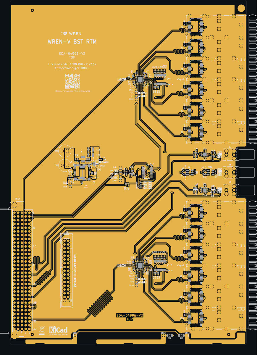
WREN V BST RTM (OHWR0095 R2) is an open-hardware circuit board from its public repository, designed in KiCad EDA: a 4-layer board of 160 × 233.4 mm with 301 components and 333 nets, published under CERN-OHL-W-2.0.
review complete · 4 findings: 3 major · 1 minor (24 items)
Open in the interactive viewerRead the full review
Design review
Probe recorded 4 findings: 3 major · 1 minor (24 items) on this design. Each is shown here with its reasoning; the full review links every one to the pins, nets and datasheet pages it rests on.
- BomLayoutMismatchmajorOpen
BomLayoutMismatch: 2 components×2
Checked by the review, stands · Claude walker R1 (cern-04 session) — NUT1/NUT2 are M2.5 nuts in CERN sheet 2 "Hardware for RP2" (with SCREW1/2, WASHER1/2) and in CERN's assembly BOM: mechanical fixing hardware for the rear connector, which by its nature has no footprint in the layout. The finding is literally true (BOM refdes not placed) and harmless; left for the owner rather than refuted.
At NUT1, NUT2
Each finding, with its own headline
- NUT1BOM refdes 'NUT1' is not placed in the layout.
- NUT2BOM refdes 'NUT2' is not placed in the layout.
- PartLifecyclemajorOpen
PCA9548APW on 2 placements (IC13, IC2): the distributor catalogue reports "Obsolete" for NXP USA Inc.'s PCA9548APW,112
PCA9548APW on 2 placements (IC13, IC2): the distributor catalogue reports "Obsolete" for NXP USA Inc.'s PCA9548APW,112 — a sourcing/longevity risk to confirm against the MANUFACTURER before acting. That is the maker this board's BOM names (NXP SEMICONDUCTORS). A distributor delisting is not the same claim as the part being unavailable; check the vendor's own lifecycle/product-change notice for the status and any named successor. Re-read the source: GET /api/odb/parts/PCA9548APW/providers (which provider said it, the maker and part number it matched, its own words, and when we asked). THE LAST BUY DATE HAS PASSED (2018-01-24, 3,217 day(s) ago), so this is a substitution rather than a buy. The distributor reports NONE left. No approved alternate is recorded for this position.
At IC13
- ReferencePlaneDiscontinuitymajorOpen
ReferencePlaneDiscontinuity: 20 boards×20
Checked by the review, stands · Claude walker R1 (cern-04 session) — Verify step, layout practice not a datasheet requirement: looked at all 20. 17 are static nets: /MODABS12 over 15 +5V outline voids and /MODABS10 along the +3.3V/+5V split on IN2.CU (SFP MOD_ABS DC levels with 4k7 pull-ups, read by polling) and /vme_power/PWRGD at one +5V/GND reference change (static open-drain), where a reference change has no signal-integrity effect. Left open for CERN: refchange:+3.3V|GND (78 nets, 130 vias), split@IN2.CU:+3.3V|+5V (11 nets) and the 0.44 mm /DATA1_OUT void edge include the 160 Mbaud DATA/TXD and 40 MHz BCLK lines; no datasheet on file sets a limit for these, so they stand as Probe raised them.
At along@IN2.CU:+3.3V|+5V, refchange:+3.3V|GND, refchange:+5V|GND, split@IN2.CU:+3.3V|+5V, void:+5V@IN2.CU:215.96,-170.95, void:+5V@IN2.CU:216.5,-189.4 and 14 more
Each finding, with its own headline
along@IN2.CU:+3.3V|+5V'/MODABS10' runs ALONG the split between the +3.3V and +5V planes on IN2.CU at 1 place, the longest 47.09 mm; the impedance rises from 49 ohm to 56 ohm there at worst, 7.4 % of each edge reflected (fastest: /MODABS10 at 100 ps 10-90 %, ASSUMED)
On IN2.CU the +3.3V and +5V planes part, and '/MODABS10' runs down the slot between them at 1 place(s), rather than across it. This is not a crossing: the return still follows the track, in the plane on its other side and in the slot's edges, so it does not detour. What changes is the track's own impedance. With the plane gone from under it on this side for that length, its field reaches further, to the slot's edges and to the next plane beyond, so its capacitance falls and its impedance rises; every edge travelling down it is partly reflected where it enters the stretch and again where it leaves, by (Z2 - Z1)/(Z2 + Z1). The longer the stretch against the edge's rise, the more of the edge sees the full step. A crossing is generally the worse fault; a mismatch is not free. Over solid plane each track is 49 ohm; along the slot 56 ohm, reflecting up to 7.4 % of each edge (a method-of-moments field solve of the cross-section, one dielectric; were the slot's edges to carry none of the return, up to 120 ohm). No place stays within 10 %, the tolerance controlled impedance is commonly built to (the stackup states none), so the finding is a warning. One decision covers the split line's slot: whether these tracks may run down it, or should be moved over solid plane.
- '/MODABS10' on B.CU at (215.5, -212.46), 47.12 mm, running ALONG the split for 47.09 mm, not across it, 49 ohm over solid plane, 56 ohm along it: 7.4 % of each edge reflected; other side: none: the signal layer is outermost
Every site is a row of this finding's evidence, keyed by net, layers and position. GET /api/odb/boards/100/reference-planes?group=along%40IN2.CU%3A%2B3.3V%7C%2B5V serves each with its own layer_image region; all of them lie in x 214.49..216.5, y -237.01..-187.9 mm (board frame, Y up).
Read from the copper as drawn on the reference layer, along each track's centreline at exact breakpoints. The reference is the copper beside the track, never the layer's type or name. Whether it matters depends on each signal's edge rate, which nothing on file states for these nets: a slow static line crosses a split harmlessly, a fast edge does not.
refchange:+3.3V|GND78 nets change reference between +3.3V and GND at 130 vias, none with a reference that continues across (fastest: /DATA1_OUT at 100 ps 10-90 %, ASSUMED)
At 130 via(s), on 78 net(s), the signal leaves a layer referenced by one of +3.3V and GND for a layer referenced by the other, and no plane references both layers. Different nets: no via can carry the return across; only decoupling between the two planes near the via can. The capacitor carrying the return across was measured at each via, at the knee of the crossing net's edge against 50 ohm assumed: 130 with none. 130 of them at an ASSUMED edge (no edge on file for the net): state one (net_timing_state) and it is re-read. One decision covers the pair: whether +3.3V and GND are decoupled to each other near these vias. A via whose layers have more references than these two is a site of each pair it joins. None is partial: at every one, no reference continues across the via.
- '/MODABS1' at (168, -167.2), F.CU -> B.CU: GND on IN1.CU to +3.3V on IN2.CU; pure, no reference continues across; stitching none, 150.4 mm of track past the via on B.CU: At the 5 GHz knee of a 100 ps edge (100 ps 10-90 %, assumed: no edge is on file for the net) no capacitor carries the return; only the planes do. +3.3V and GND are not a thin pair (at most 0.2 mm), so their own capacitance does not carry the return. To serve it, change layers across the same plane, or move the signal to a layer referenced to ground. None.
- '/MODABS1' at (204.6, -70.1), F.CU -> B.CU: GND on IN1.CU to +3.3V on IN2.CU; pure, no reference continues across; stitching none, 150.4 mm of track past the via on B.CU: At the 5 GHz knee of a 100 ps edge (100 ps 10-90 %, assumed: no edge is on file for the net) no capacitor carries the return; only the planes do. +3.3V and GND are not a thin pair (at most 0.2 mm), so their own capacitance does not carry the return. To serve it, change layers across the same plane, or move the signal to a layer referenced to ground. None.
- '/MODABS12' at (170.25, -169.5), F.CU -> B.CU: GND on IN1.CU to +3.3V on IN2.CU; pure, no reference continues across; stitching none, 148.6 mm of track past the via on B.CU: At the 5 GHz knee of a 100 ps edge (100 ps 10-90 %, assumed: no edge is on file for the net) no capacitor carries the return; only the planes do. +3.3V and GND are not a thin pair (at most 0.2 mm), so their own capacitance does not carry the return. To serve it, change layers across the same plane, or move the signal to a layer referenced to ground. None.
- '/MODABS12' at (204.6, -267.35), F.CU -> B.CU: GND on IN1.CU to +3.3V on IN2.CU; pure, no reference continues across; stitching none, 148.6 mm of track past the via on B.CU: At the 5 GHz knee of a 100 ps edge (100 ps 10-90 %, assumed: no edge is on file for the net) no capacitor carries the return; only the planes do. +3.3V and GND are not a thin pair (at most 0.2 mm), so their own capacitance does not carry the return. To serve it, change layers across the same plane, or move the signal to a layer referenced to ground. None.
- '/MODABS2' at (168.25, -167.95), F.CU -> B.CU: GND on IN1.CU to +3.3V on IN2.CU; pure, no reference continues across; stitching none, 137.4 mm of track past the via on B.CU: At the 5 GHz knee of a 100 ps edge (100 ps 10-90 %, assumed: no edge is on file for the net) no capacitor carries the return; only the planes do. +3.3V and GND are not a thin pair (at most 0.2 mm), so their own capacitance does not carry the return. To serve it, change layers across the same plane, or move the signal to a layer referenced to ground. None.
- '/MODABS2' at (204.6, -84.34), F.CU -> B.CU: GND on IN1.CU to +3.3V on IN2.CU; pure, no reference continues across; stitching none, 137.4 mm of track past the via on B.CU: At the 5 GHz knee of a 100 ps edge (100 ps 10-90 %, assumed: no edge is on file for the net) no capacitor carries the return; only the planes do. +3.3V and GND are not a thin pair (at most 0.2 mm), so their own capacitance does not carry the return. To serve it, change layers across the same plane, or move the signal to a layer referenced to ground. None.
- '/~{RESET}' at (163.25, -167), F.CU -> B.CU: GND on IN1.CU to +3.3V on IN2.CU; pure, no reference continues across; stitching none, 132.7 mm of track past the via on B.CU: At the 5 GHz knee of a 100 ps edge (20 ns 10-90 %, assumed: no edge is on file for the net) no capacitor carries the return; only the planes do. +3.3V and GND are not a thin pair (at most 0.2 mm), so their own capacitance does not carry the return. To serve it, change layers across the same plane, or move the signal to a layer referenced to ground. None.
- '/~{RESET}' at (169, -225.5), F.CU -> B.CU: GND on IN1.CU to +3.3V on IN2.CU; pure, no reference continues across; stitching none, 132.7 mm of track past the via on B.CU: At the 5 GHz knee of a 100 ps edge (20 ns 10-90 %, assumed: no edge is on file for the net) no capacitor carries the return; only the planes do. +3.3V and GND are not a thin pair (at most 0.2 mm), so their own capacitance does not carry the return. To serve it, change layers across the same plane, or move the signal to a layer referenced to ground. None.
- '/~{RESET}' at (172.9, -105.8), F.CU -> B.CU: GND on IN1.CU to +3.3V on IN2.CU; pure, no reference continues across; stitching none, 132.7 mm of track past the via on B.CU: At the 5 GHz knee of a 100 ps edge (20 ns 10-90 %, assumed: no edge is on file for the net) no capacitor carries the return; only the planes do. +3.3V and GND are not a thin pair (at most 0.2 mm), so their own capacitance does not carry the return. To serve it, change layers across the same plane, or move the signal to a layer referenced to ground. None.
- '/MODABS11' at (170.53, -170.28), F.CU -> B.CU: GND on IN1.CU to +3.3V on IN2.CU; pure, no reference continues across; stitching none, 131.1 mm of track past the via on B.CU: At the 5 GHz knee of a 100 ps edge (100 ps 10-90 %, assumed: no edge is on file for the net) no capacitor carries the return; only the planes do. +3.3V and GND are not a thin pair (at most 0.2 mm), so their own capacitance does not carry the return. To serve it, change layers across the same plane, or move the signal to a layer referenced to ground. None.
- '/MODABS11' at (204.6, -253.1), F.CU -> B.CU: GND on IN1.CU to +3.3V on IN2.CU; pure, no reference continues across; stitching none, 131.1 mm of track past the via on B.CU: At the 5 GHz knee of a 100 ps edge (100 ps 10-90 %, assumed: no edge is on file for the net) no capacitor carries the return; only the planes do. +3.3V and GND are not a thin pair (at most 0.2 mm), so their own capacitance does not carry the return. To serve it, change layers across the same plane, or move the signal to a layer referenced to ground. None.
- '/MODABS3' at (168, -168.7), F.CU -> B.CU: GND on IN1.CU to +3.3V on IN2.CU; pure, no reference continues across; stitching none, 122.9 mm of track past the via on B.CU: At the 5 GHz knee of a 100 ps edge (100 ps 10-90 %, assumed: no edge is on file for the net) no capacitor carries the return; only the planes do. +3.3V and GND are not a thin pair (at most 0.2 mm), so their own capacitance does not carry the return. To serve it, change layers across the same plane, or move the signal to a layer referenced to ground. None.
- and 118 more
Every site is a row of this finding's evidence, keyed by net, layers and position. GET /api/odb/boards/100/reference-planes?group=refchange%3A%2B3.3V%7CGND serves each with its own layer_image region; all of them lie in x 153.5..217.75, y -271.5..-66.17 mm (board frame, Y up).
The reference on each layer is the first plane the track meets leaving the via, anti-pads and the net's own copper skipped. Whether it matters depends on each signal's edge rate, which nothing on file states for these nets: a slow static line crosses a split harmlessly, a fast edge does not.
refchange:+5V|GND'/vme_power/PWRGD' changes reference between +5V and GND at a via, none with a reference that continues across (fastest: /vme_power/PWRGD at 100 ps 10-90 %, ASSUMED)
At 1 via(s), on 1 net(s), the signal leaves a layer referenced by one of +5V and GND for a layer referenced by the other, and no plane references both layers. Different nets: no via can carry the return across; only decoupling between the two planes near the via can. The capacitor carrying the return across was measured at each via, at the knee of the crossing net's edge against 50 ohm assumed: 1 with none. 1 of them at an ASSUMED edge (no edge on file for the net): state one (net_timing_state) and it is re-read. One decision covers the pair: whether +5V and GND are decoupled to each other near these vias. A via whose layers have more references than these two is a site of each pair it joins. None is partial: at every one, no reference continues across the via.
- '/vme_power/PWRGD' at (119.25, -170.25), F.CU -> B.CU: GND on IN1.CU to +5V on IN2.CU; pure, no reference continues across; stitching none, 43.7 mm of track past the via on B.CU: At the 5 GHz knee of a 100 ps edge (100 ps 10-90 %, assumed: no edge is on file for the net) no capacitor carries the return; only the planes do. +5V and GND are not a thin pair (at most 0.2 mm), so their own capacitance does not carry the return. To serve it, change layers across the same plane, or move the signal to a layer referenced to ground. Measured for reference: C43 (22 uF 0603) 2.6 mm away: 1.44 nH in the 1.200 mm cavity + 0.51 nH ESL + 0.88 nH mounting (pad 0.10 nH + no via of the first net within 1 mm of its pad: the study's 0.6 nH per mm of 1.30 mm depth, ASSUMED): 89.0 ohm at the knee, 178 % of 50 ohm (assumed track impedance). None.
Every site is a row of this finding's evidence, keyed by net, layers and position. GET /api/odb/boards/100/reference-planes?group=refchange%3A%2B5V%7CGND serves each with its own layer_image region; all of them lie in x 117.25..121.25, y -172.25..-168.25 mm (board frame, Y up).
The reference on each layer is the first plane the track meets leaving the via, anti-pads and the net's own copper skipped. Whether it matters depends on each signal's edge rate, which nothing on file states for these nets: a slow static line crosses a split harmlessly, a fast edge does not.
split@IN2.CU:+3.3V|+5V11 nets cross the split between the +3.3V and +5V planes on IN2.CU at 14 places, with no plane on the track's other side (fastest: /DATA1_OUT at 100 ps 10-90 %, ASSUMED)
On IN2.CU the +3.3V and +5V planes part, and 11 nets cross from one to the other at 14 place(s). The return current cannot follow a track across; it detours to wherever the two planes are joined (a stitching capacitor, or the source), and the loop it opens radiates and couples. One decision covers the boundary: whether it is stitched near these crossings, or the nets crossing it are slow enough not to care. Tracks that run ALONG this split, down the slot rather than across it, are a finding of their own: theirs is an impedance step, not a detour. At 0 of the 14 crossing(s) the track's other neighbour carries a plane, which the return can use there; 14 are on an outer layer, with no other neighbour. No crossing has a plane on the track's other side, so the whole return meets the break.
- '/BCLK1_OUT' on B.CU at (215.75, -157), 0.51 mm; other side: none: the signal layer is outermost
- '/BCLK2_OUT' on B.CU at (215.75, -181), 0.51 mm; other side: none: the signal layer is outermost
- '/DATA1_OUT' on B.CU at (215.7, -170.39), 0.78 mm; other side: none: the signal layer is outermost
- '/DATA2_OUT' on B.CU at (215.75, -173.25), 0.51 mm; other side: none: the signal layer is outermost
- '/MODABS1' on B.CU at (215.88, -152.63), 0.61 mm; other side: none: the signal layer is outermost
- '/MODABS1' on B.CU at (216.76, -151.75), 0.72 mm; other side: none: the signal layer is outermost
- '/MODABS11' on B.CU at (215.75, -248.51), 0.72 mm; other side: none: the signal layer is outermost
- '/MODABS11' on B.CU at (215.75, -188.46), 0.72 mm; other side: none: the signal layer is outermost
- '/MODABS12' on B.CU at (215.75, -264.26), 0.72 mm; other side: none: the signal layer is outermost
- '/MODABS12' on B.CU at (215.75, -187.75), 0.72 mm; other side: none: the signal layer is outermost
- '/MODABS2' on B.CU at (215.92, -151.87), 1.12 mm; other side: none: the signal layer is outermost
- '/TCLK1_OUT' on B.CU at (215.75, -154.75), 0.51 mm; other side: none: the signal layer is outermost
- and 2 more
Every site is a row of this finding's evidence, keyed by net, layers and position. GET /api/odb/boards/100/reference-planes?group=split%40IN2.CU%3A%2B3.3V%7C%2B5V serves each with its own layer_image region; all of them lie in x 122.75..218.01, y -265.51..-150.49 mm (board frame, Y up).
Read from the copper as drawn on the reference layer, along each track's centreline at exact breakpoints. The reference is the copper beside the track, never the layer's type or name. Whether it matters depends on each signal's edge rate, which nothing on file states for these nets: a slow static line crosses a split harmlessly, a fast edge does not.
void:+5V@IN2.CU:215.96,-170.95'/DATA1_OUT' crosses where the outline of the +5V plane on IN2.CU is drawn back, at 1 place, the longest 0.44 mm (fastest: /DATA1_OUT at 100 ps 10-90 %, ASSUMED)
Along '/DATA1_OUT' on B.CU, the +5V plane on IN2.CU has 0.44 mm under the track with no copper, at (215.96, -170.95), running to the end of the track. No single drill's anti-pad and no landing explains it: a clearance is excused only when it holds a drill and is drawn round it, or the track ends in it on the net's own pad or via, or runs through its own via's clearance and no farther. The return current detours round the void. No hole cleared it: the outline of the pour at x 123.75..236.11, y -282.14..-152 is drawn back there. One decision covers the void: whether these tracks may cross it, or the plane should be filled under them. No crossing has a plane on the track's other side, so the whole return meets the break.
- '/DATA1_OUT' on B.CU at (215.96, -170.95), 0.44 mm over no copper, to the end of the track; other side: none: the signal layer is outermost
Every site is a row of this finding's evidence, keyed by net, layers and position. GET /api/odb/boards/100/reference-planes?group=void%3A%2B5V%40IN2.CU%3A215.96%2C-170.95 serves each with its own layer_image region; all of them lie in x 214.69..217, y -171.95..-169.72 mm (board frame, Y up).
Read from the copper as drawn on the reference layer, along each track's centreline at exact breakpoints. The reference is the copper beside the track, never the layer's type or name. Whether it matters depends on each signal's edge rate, which nothing on file states for these nets: a slow static line crosses a split harmlessly, a fast edge does not.
void:+5V@IN2.CU:216.5,-189.4'/MODABS12' crosses where the outline of the +5V plane on IN2.CU is drawn back, at 1 place, the longest 1.8 mm (fastest: /MODABS12 at 100 ps 10-90 %, ASSUMED)
Along '/MODABS12' on B.CU, the +5V plane on IN2.CU has 1.8 mm under the track with no copper, at (216.5, -189.4), the same plane on both sides. No single drill's anti-pad and no landing explains it: a clearance is excused only when it holds a drill and is drawn round it, or the track ends in it on the net's own pad or via, or runs through its own via's clearance and no farther. The return current detours round the void. 1 of them run ALONG the bare copper, parallel to its edges, rather than across it (the longest 1.8 mm). No hole cleared it: the outline of the pour at x 123.75..236.11, y -282.14..-152 is drawn back there. One decision covers the void: whether these tracks may cross it, or the plane should be filled under them. No crossing has a plane on the track's other side, so the whole return meets the break.
- '/MODABS12' on B.CU at (216.5, -189.4), 1.8 mm, running ALONG the bare copper for 1.8 mm, not across it over no copper; other side: none: the signal layer is outermost
Every site is a row of this finding's evidence, keyed by net, layers and position. GET /api/odb/boards/100/reference-planes?group=void%3A%2B5V%40IN2.CU%3A216.5%2C-189.4 serves each with its own layer_image region; all of them lie in x 215.5..217.5, y -191.3..-187.5 mm (board frame, Y up).
Read from the copper as drawn on the reference layer, along each track's centreline at exact breakpoints. The reference is the copper beside the track, never the layer's type or name. Whether it matters depends on each signal's edge rate, which nothing on file states for these nets: a slow static line crosses a split harmlessly, a fast edge does not.
void:+5V@IN2.CU:216.5,-192.43'/MODABS12' crosses where the outline of the +5V plane on IN2.CU is drawn back, at 1 place, the longest 2.09 mm (fastest: /MODABS12 at 100 ps 10-90 %, ASSUMED)
Along '/MODABS12' on B.CU, the +5V plane on IN2.CU has 2.09 mm under the track with no copper, at (216.5, -192.43), the same plane on both sides. No single drill's anti-pad and no landing explains it: a clearance is excused only when it holds a drill and is drawn round it, or the track ends in it on the net's own pad or via, or runs through its own via's clearance and no farther. The return current detours round the void. 1 of them run ALONG the bare copper, parallel to its edges, rather than across it (the longest 2.09 mm). No hole cleared it: the outline of the pour at x 123.75..236.11, y -282.14..-152 is drawn back there. One decision covers the void: whether these tracks may cross it, or the plane should be filled under them. No crossing has a plane on the track's other side, so the whole return meets the break.
- '/MODABS12' on B.CU at (216.5, -192.43), 2.09 mm, running ALONG the bare copper for 2.09 mm, not across it over no copper; other side: none: the signal layer is outermost
Every site is a row of this finding's evidence, keyed by net, layers and position. GET /api/odb/boards/100/reference-planes?group=void%3A%2B5V%40IN2.CU%3A216.5%2C-192.43 serves each with its own layer_image region; all of them lie in x 215.5..217.5, y -194.47..-190.38 mm (board frame, Y up).
Read from the copper as drawn on the reference layer, along each track's centreline at exact breakpoints. The reference is the copper beside the track, never the layer's type or name. Whether it matters depends on each signal's edge rate, which nothing on file states for these nets: a slow static line crosses a split harmlessly, a fast edge does not.
void:+5V@IN2.CU:216.5,-197.81'/MODABS12' crosses where the outline of the +5V plane on IN2.CU is drawn back, at 1 place, the longest 2.12 mm (fastest: /MODABS12 at 100 ps 10-90 %, ASSUMED)
Along '/MODABS12' on B.CU, the +5V plane on IN2.CU has 2.12 mm under the track with no copper, at (216.5, -197.81), the same plane on both sides. No single drill's anti-pad and no landing explains it: a clearance is excused only when it holds a drill and is drawn round it, or the track ends in it on the net's own pad or via, or runs through its own via's clearance and no farther. The return current detours round the void. 1 of them run ALONG the bare copper, parallel to its edges, rather than across it (the longest 2.12 mm). No hole cleared it: the outline of the pour at x 123.75..236.11, y -282.14..-152 is drawn back there. One decision covers the void: whether these tracks may cross it, or the plane should be filled under them. No crossing has a plane on the track's other side, so the whole return meets the break.
- '/MODABS12' on B.CU at (216.5, -197.81), 2.12 mm, running ALONG the bare copper for 2.12 mm, not across it over no copper; other side: none: the signal layer is outermost
Every site is a row of this finding's evidence, keyed by net, layers and position. GET /api/odb/boards/100/reference-planes?group=void%3A%2B5V%40IN2.CU%3A216.5%2C-197.81 serves each with its own layer_image region; all of them lie in x 215.5..217.5, y -199.87..-195.75 mm (board frame, Y up).
Read from the copper as drawn on the reference layer, along each track's centreline at exact breakpoints. The reference is the copper beside the track, never the layer's type or name. Whether it matters depends on each signal's edge rate, which nothing on file states for these nets: a slow static line crosses a split harmlessly, a fast edge does not.
void:+5V@IN2.CU:216.5,-206.67'/MODABS12' crosses where the outline of the +5V plane on IN2.CU is drawn back, at 1 place, the longest 2.11 mm (fastest: /MODABS12 at 100 ps 10-90 %, ASSUMED)
Along '/MODABS12' on B.CU, the +5V plane on IN2.CU has 2.11 mm under the track with no copper, at (216.5, -206.67), the same plane on both sides. No single drill's anti-pad and no landing explains it: a clearance is excused only when it holds a drill and is drawn round it, or the track ends in it on the net's own pad or via, or runs through its own via's clearance and no farther. The return current detours round the void. 1 of them run ALONG the bare copper, parallel to its edges, rather than across it (the longest 2.11 mm). No hole cleared it: the outline of the pour at x 123.75..236.11, y -282.14..-152 is drawn back there. One decision covers the void: whether these tracks may cross it, or the plane should be filled under them. No crossing has a plane on the track's other side, so the whole return meets the break.
- '/MODABS12' on B.CU at (216.5, -206.67), 2.11 mm, running ALONG the bare copper for 2.11 mm, not across it over no copper; other side: none: the signal layer is outermost
Every site is a row of this finding's evidence, keyed by net, layers and position. GET /api/odb/boards/100/reference-planes?group=void%3A%2B5V%40IN2.CU%3A216.5%2C-206.67 serves each with its own layer_image region; all of them lie in x 215.5..217.5, y -208.72..-204.61 mm (board frame, Y up).
Read from the copper as drawn on the reference layer, along each track's centreline at exact breakpoints. The reference is the copper beside the track, never the layer's type or name. Whether it matters depends on each signal's edge rate, which nothing on file states for these nets: a slow static line crosses a split harmlessly, a fast edge does not.
void:+5V@IN2.CU:216.5,-212.07'/MODABS12' crosses where the outline of the +5V plane on IN2.CU is drawn back, at 1 place, the longest 2.1 mm (fastest: /MODABS12 at 100 ps 10-90 %, ASSUMED)
Along '/MODABS12' on B.CU, the +5V plane on IN2.CU has 2.1 mm under the track with no copper, at (216.5, -212.07), the same plane on both sides. No single drill's anti-pad and no landing explains it: a clearance is excused only when it holds a drill and is drawn round it, or the track ends in it on the net's own pad or via, or runs through its own via's clearance and no farther. The return current detours round the void. 1 of them run ALONG the bare copper, parallel to its edges, rather than across it (the longest 2.1 mm). No hole cleared it: the outline of the pour at x 123.75..236.11, y -282.14..-152 is drawn back there. One decision covers the void: whether these tracks may cross it, or the plane should be filled under them. No crossing has a plane on the track's other side, so the whole return meets the break.
- '/MODABS12' on B.CU at (216.5, -212.07), 2.1 mm, running ALONG the bare copper for 2.1 mm, not across it over no copper; other side: none: the signal layer is outermost
Every site is a row of this finding's evidence, keyed by net, layers and position. GET /api/odb/boards/100/reference-planes?group=void%3A%2B5V%40IN2.CU%3A216.5%2C-212.07 serves each with its own layer_image region; all of them lie in x 215.5..217.5, y -214.12..-210.02 mm (board frame, Y up).
Read from the copper as drawn on the reference layer, along each track's centreline at exact breakpoints. The reference is the copper beside the track, never the layer's type or name. Whether it matters depends on each signal's edge rate, which nothing on file states for these nets: a slow static line crosses a split harmlessly, a fast edge does not.
void:+5V@IN2.CU:216.5,-217.74'/MODABS12' crosses where the outline of the +5V plane on IN2.CU is drawn back, at 1 place, the longest 2.13 mm (fastest: /MODABS12 at 100 ps 10-90 %, ASSUMED)
Along '/MODABS12' on B.CU, the +5V plane on IN2.CU has 2.13 mm under the track with no copper, at (216.5, -217.74), the same plane on both sides. No single drill's anti-pad and no landing explains it: a clearance is excused only when it holds a drill and is drawn round it, or the track ends in it on the net's own pad or via, or runs through its own via's clearance and no farther. The return current detours round the void. 1 of them run ALONG the bare copper, parallel to its edges, rather than across it (the longest 2.13 mm). No hole cleared it: the outline of the pour at x 123.75..236.11, y -282.14..-152 is drawn back there. One decision covers the void: whether these tracks may cross it, or the plane should be filled under them. No crossing has a plane on the track's other side, so the whole return meets the break.
- '/MODABS12' on B.CU at (216.5, -217.74), 2.13 mm, running ALONG the bare copper for 2.13 mm, not across it over no copper; other side: none: the signal layer is outermost
Every site is a row of this finding's evidence, keyed by net, layers and position. GET /api/odb/boards/100/reference-planes?group=void%3A%2B5V%40IN2.CU%3A216.5%2C-217.74 serves each with its own layer_image region; all of them lie in x 215.5..217.5, y -219.8..-215.67 mm (board frame, Y up).
Read from the copper as drawn on the reference layer, along each track's centreline at exact breakpoints. The reference is the copper beside the track, never the layer's type or name. Whether it matters depends on each signal's edge rate, which nothing on file states for these nets: a slow static line crosses a split harmlessly, a fast edge does not.
void:+5V@IN2.CU:216.5,-220.92'/MODABS12' crosses where the outline of the +5V plane on IN2.CU is drawn back, at 1 place, the longest 2.1 mm (fastest: /MODABS12 at 100 ps 10-90 %, ASSUMED)
Along '/MODABS12' on B.CU, the +5V plane on IN2.CU has 2.1 mm under the track with no copper, at (216.5, -220.92), the same plane on both sides. No single drill's anti-pad and no landing explains it: a clearance is excused only when it holds a drill and is drawn round it, or the track ends in it on the net's own pad or via, or runs through its own via's clearance and no farther. The return current detours round the void. 1 of them run ALONG the bare copper, parallel to its edges, rather than across it (the longest 2.1 mm). No hole cleared it: the outline of the pour at x 123.75..236.11, y -282.14..-152 is drawn back there. One decision covers the void: whether these tracks may cross it, or the plane should be filled under them. No crossing has a plane on the track's other side, so the whole return meets the break.
- '/MODABS12' on B.CU at (216.5, -220.92), 2.1 mm, running ALONG the bare copper for 2.1 mm, not across it over no copper; other side: none: the signal layer is outermost
Every site is a row of this finding's evidence, keyed by net, layers and position. GET /api/odb/boards/100/reference-planes?group=void%3A%2B5V%40IN2.CU%3A216.5%2C-220.92 serves each with its own layer_image region; all of them lie in x 215.5..217.5, y -222.97..-218.87 mm (board frame, Y up).
Read from the copper as drawn on the reference layer, along each track's centreline at exact breakpoints. The reference is the copper beside the track, never the layer's type or name. Whether it matters depends on each signal's edge rate, which nothing on file states for these nets: a slow static line crosses a split harmlessly, a fast edge does not.
void:+5V@IN2.CU:216.5,-226.32'/MODABS12' crosses where the outline of the +5V plane on IN2.CU is drawn back, at 1 place, the longest 2.11 mm (fastest: /MODABS12 at 100 ps 10-90 %, ASSUMED)
Along '/MODABS12' on B.CU, the +5V plane on IN2.CU has 2.11 mm under the track with no copper, at (216.5, -226.32), the same plane on both sides. No single drill's anti-pad and no landing explains it: a clearance is excused only when it holds a drill and is drawn round it, or the track ends in it on the net's own pad or via, or runs through its own via's clearance and no farther. The return current detours round the void. 1 of them run ALONG the bare copper, parallel to its edges, rather than across it (the longest 2.11 mm). No hole cleared it: the outline of the pour at x 123.75..236.11, y -282.14..-152 is drawn back there. One decision covers the void: whether these tracks may cross it, or the plane should be filled under them. No crossing has a plane on the track's other side, so the whole return meets the break.
- '/MODABS12' on B.CU at (216.5, -226.32), 2.11 mm, running ALONG the bare copper for 2.11 mm, not across it over no copper; other side: none: the signal layer is outermost
Every site is a row of this finding's evidence, keyed by net, layers and position. GET /api/odb/boards/100/reference-planes?group=void%3A%2B5V%40IN2.CU%3A216.5%2C-226.32 serves each with its own layer_image region; all of them lie in x 215.5..217.5, y -228.37..-224.26 mm (board frame, Y up).
Read from the copper as drawn on the reference layer, along each track's centreline at exact breakpoints. The reference is the copper beside the track, never the layer's type or name. Whether it matters depends on each signal's edge rate, which nothing on file states for these nets: a slow static line crosses a split harmlessly, a fast edge does not.
void:+5V@IN2.CU:216.5,-232'/MODABS12' crosses where the outline of the +5V plane on IN2.CU is drawn back, at 1 place, the longest 2.1 mm (fastest: /MODABS12 at 100 ps 10-90 %, ASSUMED)
Along '/MODABS12' on B.CU, the +5V plane on IN2.CU has 2.1 mm under the track with no copper, at (216.5, -232), the same plane on both sides. No single drill's anti-pad and no landing explains it: a clearance is excused only when it holds a drill and is drawn round it, or the track ends in it on the net's own pad or via, or runs through its own via's clearance and no farther. The return current detours round the void. 1 of them run ALONG the bare copper, parallel to its edges, rather than across it (the longest 2.1 mm). No hole cleared it: the outline of the pour at x 123.75..236.11, y -282.14..-152 is drawn back there. One decision covers the void: whether these tracks may cross it, or the plane should be filled under them. No crossing has a plane on the track's other side, so the whole return meets the break.
- '/MODABS12' on B.CU at (216.5, -232), 2.1 mm, running ALONG the bare copper for 2.1 mm, not across it over no copper; other side: none: the signal layer is outermost
Every site is a row of this finding's evidence, keyed by net, layers and position. GET /api/odb/boards/100/reference-planes?group=void%3A%2B5V%40IN2.CU%3A216.5%2C-232 serves each with its own layer_image region; all of them lie in x 215.5..217.5, y -234.05..-229.95 mm (board frame, Y up).
Read from the copper as drawn on the reference layer, along each track's centreline at exact breakpoints. The reference is the copper beside the track, never the layer's type or name. Whether it matters depends on each signal's edge rate, which nothing on file states for these nets: a slow static line crosses a split harmlessly, a fast edge does not.
void:+5V@IN2.CU:216.5,-235.18'/MODABS12' crosses where the outline of the +5V plane on IN2.CU is drawn back, at 1 place, the longest 2.09 mm (fastest: /MODABS12 at 100 ps 10-90 %, ASSUMED)
Along '/MODABS12' on B.CU, the +5V plane on IN2.CU has 2.09 mm under the track with no copper, at (216.5, -235.18), the same plane on both sides. No single drill's anti-pad and no landing explains it: a clearance is excused only when it holds a drill and is drawn round it, or the track ends in it on the net's own pad or via, or runs through its own via's clearance and no farther. The return current detours round the void. 1 of them run ALONG the bare copper, parallel to its edges, rather than across it (the longest 2.09 mm). No hole cleared it: the outline of the pour at x 123.75..236.11, y -282.14..-152 is drawn back there. One decision covers the void: whether these tracks may cross it, or the plane should be filled under them. No crossing has a plane on the track's other side, so the whole return meets the break.
- '/MODABS12' on B.CU at (216.5, -235.18), 2.09 mm, running ALONG the bare copper for 2.09 mm, not across it over no copper; other side: none: the signal layer is outermost
Every site is a row of this finding's evidence, keyed by net, layers and position. GET /api/odb/boards/100/reference-planes?group=void%3A%2B5V%40IN2.CU%3A216.5%2C-235.18 serves each with its own layer_image region; all of them lie in x 215.5..217.5, y -237.22..-233.13 mm (board frame, Y up).
Read from the copper as drawn on the reference layer, along each track's centreline at exact breakpoints. The reference is the copper beside the track, never the layer's type or name. Whether it matters depends on each signal's edge rate, which nothing on file states for these nets: a slow static line crosses a split harmlessly, a fast edge does not.
void:+5V@IN2.CU:216.5,-240.57'/MODABS12' crosses where the outline of the +5V plane on IN2.CU is drawn back, at 1 place, the longest 2.1 mm (fastest: /MODABS12 at 100 ps 10-90 %, ASSUMED)
Along '/MODABS12' on B.CU, the +5V plane on IN2.CU has 2.1 mm under the track with no copper, at (216.5, -240.57), the same plane on both sides. No single drill's anti-pad and no landing explains it: a clearance is excused only when it holds a drill and is drawn round it, or the track ends in it on the net's own pad or via, or runs through its own via's clearance and no farther. The return current detours round the void. 1 of them run ALONG the bare copper, parallel to its edges, rather than across it (the longest 2.1 mm). No hole cleared it: the outline of the pour at x 123.75..236.11, y -282.14..-152 is drawn back there. One decision covers the void: whether these tracks may cross it, or the plane should be filled under them. No crossing has a plane on the track's other side, so the whole return meets the break.
- '/MODABS12' on B.CU at (216.5, -240.57), 2.1 mm, running ALONG the bare copper for 2.1 mm, not across it over no copper; other side: none: the signal layer is outermost
Every site is a row of this finding's evidence, keyed by net, layers and position. GET /api/odb/boards/100/reference-planes?group=void%3A%2B5V%40IN2.CU%3A216.5%2C-240.57 serves each with its own layer_image region; all of them lie in x 215.5..217.5, y -242.62..-238.52 mm (board frame, Y up).
Read from the copper as drawn on the reference layer, along each track's centreline at exact breakpoints. The reference is the copper beside the track, never the layer's type or name. Whether it matters depends on each signal's edge rate, which nothing on file states for these nets: a slow static line crosses a split harmlessly, a fast edge does not.
void:+5V@IN2.CU:216.5,-249.42'/MODABS12' crosses where the outline of the +5V plane on IN2.CU is drawn back, at 1 place, the longest 2.1 mm (fastest: /MODABS12 at 100 ps 10-90 %, ASSUMED)
Along '/MODABS12' on B.CU, the +5V plane on IN2.CU has 2.1 mm under the track with no copper, at (216.5, -249.42), the same plane on both sides. No single drill's anti-pad and no landing explains it: a clearance is excused only when it holds a drill and is drawn round it, or the track ends in it on the net's own pad or via, or runs through its own via's clearance and no farther. The return current detours round the void. 1 of them run ALONG the bare copper, parallel to its edges, rather than across it (the longest 2.1 mm). No hole cleared it: the outline of the pour at x 123.75..236.11, y -282.14..-152 is drawn back there. One decision covers the void: whether these tracks may cross it, or the plane should be filled under them. No crossing has a plane on the track's other side, so the whole return meets the break.
- '/MODABS12' on B.CU at (216.5, -249.42), 2.1 mm, running ALONG the bare copper for 2.1 mm, not across it over no copper; other side: none: the signal layer is outermost
Every site is a row of this finding's evidence, keyed by net, layers and position. GET /api/odb/boards/100/reference-planes?group=void%3A%2B5V%40IN2.CU%3A216.5%2C-249.42 serves each with its own layer_image region; all of them lie in x 215.5..217.5, y -251.47..-247.37 mm (board frame, Y up).
Read from the copper as drawn on the reference layer, along each track's centreline at exact breakpoints. The reference is the copper beside the track, never the layer's type or name. Whether it matters depends on each signal's edge rate, which nothing on file states for these nets: a slow static line crosses a split harmlessly, a fast edge does not.
void:+5V@IN2.CU:216.5,-254.82'/MODABS12' crosses where the outline of the +5V plane on IN2.CU is drawn back, at 1 place, the longest 2.1 mm (fastest: /MODABS12 at 100 ps 10-90 %, ASSUMED)
Along '/MODABS12' on B.CU, the +5V plane on IN2.CU has 2.1 mm under the track with no copper, at (216.5, -254.82), the same plane on both sides. No single drill's anti-pad and no landing explains it: a clearance is excused only when it holds a drill and is drawn round it, or the track ends in it on the net's own pad or via, or runs through its own via's clearance and no farther. The return current detours round the void. 1 of them run ALONG the bare copper, parallel to its edges, rather than across it (the longest 2.1 mm). No hole cleared it: the outline of the pour at x 123.75..236.11, y -282.14..-152 is drawn back there. One decision covers the void: whether these tracks may cross it, or the plane should be filled under them. No crossing has a plane on the track's other side, so the whole return meets the break.
- '/MODABS12' on B.CU at (216.5, -254.82), 2.1 mm, running ALONG the bare copper for 2.1 mm, not across it over no copper; other side: none: the signal layer is outermost
Every site is a row of this finding's evidence, keyed by net, layers and position. GET /api/odb/boards/100/reference-planes?group=void%3A%2B5V%40IN2.CU%3A216.5%2C-254.82 serves each with its own layer_image region; all of them lie in x 215.5..217.5, y -256.87..-252.77 mm (board frame, Y up).
Read from the copper as drawn on the reference layer, along each track's centreline at exact breakpoints. The reference is the copper beside the track, never the layer's type or name. Whether it matters depends on each signal's edge rate, which nothing on file states for these nets: a slow static line crosses a split harmlessly, a fast edge does not.
void:+5V@IN2.CU:216.5,-260.5'/MODABS12' crosses where the outline of the +5V plane on IN2.CU is drawn back, at 1 place, the longest 2.1 mm (fastest: /MODABS12 at 100 ps 10-90 %, ASSUMED)
Along '/MODABS12' on B.CU, the +5V plane on IN2.CU has 2.1 mm under the track with no copper, at (216.5, -260.5), the same plane on both sides. No single drill's anti-pad and no landing explains it: a clearance is excused only when it holds a drill and is drawn round it, or the track ends in it on the net's own pad or via, or runs through its own via's clearance and no farther. The return current detours round the void. 1 of them run ALONG the bare copper, parallel to its edges, rather than across it (the longest 2.1 mm). No hole cleared it: the outline of the pour at x 123.75..236.11, y -282.14..-152 is drawn back there. One decision covers the void: whether these tracks may cross it, or the plane should be filled under them. No crossing has a plane on the track's other side, so the whole return meets the break.
- '/MODABS12' on B.CU at (216.5, -260.5), 2.1 mm, running ALONG the bare copper for 2.1 mm, not across it over no copper; other side: none: the signal layer is outermost
Every site is a row of this finding's evidence, keyed by net, layers and position. GET /api/odb/boards/100/reference-planes?group=void%3A%2B5V%40IN2.CU%3A216.5%2C-260.5 serves each with its own layer_image region; all of them lie in x 215.5..217.5, y -262.55..-258.45 mm (board frame, Y up).
Read from the copper as drawn on the reference layer, along each track's centreline at exact breakpoints. The reference is the copper beside the track, never the layer's type or name. Whether it matters depends on each signal's edge rate, which nothing on file states for these nets: a slow static line crosses a split harmlessly, a fast edge does not.
void:+5V@IN2.CU:216.5,-263.06'/MODABS12' crosses where the outline of the +5V plane on IN2.CU is drawn back, at 1 place, the longest 0.88 mm (fastest: /MODABS12 at 100 ps 10-90 %, ASSUMED)
Along '/MODABS12' on B.CU, the +5V plane on IN2.CU has 0.88 mm under the track with no copper, at (216.5, -263.06), the same plane on both sides. No single drill's anti-pad and no landing explains it: a clearance is excused only when it holds a drill and is drawn round it, or the track ends in it on the net's own pad or via, or runs through its own via's clearance and no farther. The return current detours round the void. 1 of them run ALONG the bare copper, parallel to its edges, rather than across it (the longest 0.88 mm). No hole cleared it: the outline of the pour at x 123.75..236.11, y -282.14..-152 is drawn back there. One decision covers the void: whether these tracks may cross it, or the plane should be filled under them. No crossing has a plane on the track's other side, so the whole return meets the break.
- '/MODABS12' on B.CU at (216.5, -263.06), 0.88 mm, running ALONG the bare copper for 0.88 mm, not across it over no copper; other side: none: the signal layer is outermost
Every site is a row of this finding's evidence, keyed by net, layers and position. GET /api/odb/boards/100/reference-planes?group=void%3A%2B5V%40IN2.CU%3A216.5%2C-263.06 serves each with its own layer_image region; all of them lie in x 215.5..217.5, y -264.5..-261.62 mm (board frame, Y up).
Read from the copper as drawn on the reference layer, along each track's centreline at exact breakpoints. The reference is the copper beside the track, never the layer's type or name. Whether it matters depends on each signal's edge rate, which nothing on file states for these nets: a slow static line crosses a split harmlessly, a fast edge does not.
+3.3V load can exceed IC6 LMZ31704's 4 A rating with 12 Power Level I SFP+ modules fitted
IC6 (LMZ31704, +5V to +3.3V) is rated for 4 A, but twelve SFP+ cages and two SY58031U fan-out buffers on +3.3V can ask for about 4.3 A worst case: the margin depends on which modules are fitted.
The budget at the published maxima
Load on +3.3V Each Count Total Source SFP+ module, Power Level I (J1-J6, J10-J12, J14-J16) 1.0 W = 0.30 A at 3.3 V 12 3.64 A SFF-8431 Rev 4.1, section 2.8, p17 SY58031U 1:8 CML fan-out (IC1, IC12) 330 mA max 2 0.66 A SY58031U datasheet p4, I_CC NBA3N012C, SN74LVTH125, PCA9548A, PCA9539A, 24AA025, LD1 small not counted Sum about 4.30 A derived LMZ31704 rated output current 4 A (85 C, natural convection) LMZ31704 datasheet SLVSBV8E p4 Every SFP+ VCCT/VCCR pin is fed from +3.3V through a BLM21PG221SN1 bead (L1-L24, sheets 3-4), and +3.3V has no other producer than IC6 (sheet 2).
``
mermaid graph LR P2["RP2 row b +5V"] --> IC6["IC6 LMZ31704, 4 A"] IC6 --> R33["+3.3V"] R33 --> SFP["12 x SFP+ VCCT/VCCR via L1-L24, up to 3.64 A"] R33 --> SY["IC1, IC12 SY58031U, up to 0.66 A"]``Why it matters
With modules drawing their Power Level I limit, the module is past its rated output current (its 9 A current limit will not trip, so it runs hot rather than shutting down). Typical module power is usually lower, so this is a margin question, not a certain overload. Power Level II modules (up to 1.5 W) would make it worse, but SFF-8431 says they stay at 1.0 W until the host enables Level II over I2C.
Question for CERN
Is the module type fitted in these cages (and its maximum power) part of the BST RTM specification? If modules up to 1.0 W are allowed in all twelve cages, the 3.3 V converter needs a larger rating or a second converter.
Main parts
| Part number | Maker | Description | Where |
|---|---|---|---|
| 02 04 160 1101 | HARTING | DIN 41612, har-bus 64, 160 poles, 5 Rows z+a+b+c+d, Angled solder pins, Female contacts Pitch 2.54mm, Performance level 1 | RP2 |
| 232270671609L | YAGEO PHYCOMP | ±1% 0.0625W ±100ppm/°C General Purpose Thick Film Chip Resistor | R21 |
| 232270673001L | YAGEO PHYCOMP | ±1% 0.0625W ±100ppm/°C General Purpose Thick Film Chip Resistor | R25 |
| 24AA025E48T-I/OT | MICROCHIP TECHNOLOGY | 1.7V-5.5V, 2K I2C Serial EEPROM with EUI-48™ Node Identity; Cascadable | IC7 |
| CRCW040290K9FK | VISHAY | ±1% 0.063W ±100ppm/°C General Purpose Thick Film Chip Resistor | R26 |
| GRM32ER71A476KE15 | MURATA | ±10% 10V X7R SMD Multilayer Chip Ceramic Capacitor | C26 |
| KPH-1608CGCK | KINGBRIGHT | SMD Green LED, Case 1.6mmX0.8mm(0603), 0.65mm Thickness | LD1 |
| LMZ31704RVQT | TEXAS INSTRUMENTS | 4A SIMPLE SWITCHER® Power Module with 2.95V-17V Input and Current Sharing in QFN Package | IC6 |
| PCA9539APW | NXP SEMICONDUCTORS | Low-Voltage 16-Bit I2C-Bus I/O Port with Interrupt and Reset | IC8 |
| 2007251-1 | TYCO ELECTRONICS | 1x6 Press Fit SFP+ Cage with EMI Springs | Cage1, Cage2 |
| C1005X7R1E105K050 | TDK | ±10% 10V X7R SMD Multilayer Chip Ceramic Capacitor | C29, C45 |
| GRM32ER60J227ME05L | MURATA | ±20% 6.3V X5R SMD Multilayer Chip Ceramic Capacitor | C18, C22 |
| NRC12F1004TRF | NIC COMPONENT | ±1% 0.25W ±100ppm/°C General Purpose Thick Film Chip Resistor | R52, R53 |
| PCA9548APW | NXP SEMICONDUCTORS | 8-Channel I2C-Bus Switch with Reset | IC13, IC2 |
| PRTR5V0U2X | NXP SEMICONDUCTORS | 5.5V Ultra Low Capacitance (1pF) Double Rail-to-Rail ESD Protection Diode (8kV) | D1, D2 |
| RL81V101MDN1KX | NICHICON | ±20% 35V Ultra Low ESR 0R025 Functional Polymer Aluminum Solid Electrolytic Capacitor (L8 Series) | C21, C31 |
| SN74LVTH125RGY | TEXAS INSTRUMENTS | 3.3V ABT Quadruple Bus Buffer with 3-State Outputs | IC10, IC4 |
| SY58031UM | MICREL | Ultra-Precision1:8 Differential CML Fanout Buffer with Internal I/O Termination | IC1, IC12 |
| TCM2-43X+ | MINI-CIRCUITS | 0.4W 50 Ohms 10 to 4000MHz RF Transformer | TR1, TR2 |
| EPY.00.250.NTNY | LEMO | Size 00 ,Low Profile Dual 50 Ohms Coaxial Elbow Sockets (90°) | J7, J8, J9 |
| 232270591001L | YAGEO PHYCOMP | 1A (0.05R Max DC Resistance) Zero Ohm Jumper | R22, R23, R28, R29 |
| GRM1555C1HR50WA01 | MURATA | ±0.05pF 50V C0G/NP0 Chip Multilayer Ceramic Capacitor for General Purpose | C33, C34, C39, C40 |
| NBA3N012CSN | ON SEMICONDUCTOR | 3.3 V, Automotive Grade, LVDS Line Receiver | IC11, IC3, IC5, IC9 |
| 232270464708L or RC0603FR-074R7L | YAGEO PHYCOMP | ±1% 0.1W ±200ppm/°C General Purpose Thick Film Chip Resistor | R72, R73, R74, R75, R76, R77, R78, R79 |
| 1888247-1 | TYCO ELECTRONICS | 20 Position, Pitch 0.8mm SFP+ Receptacle (Small Form-factor Pluggable) | J1, J10, J11, J12, J14, J15 and 6 more |
| 232270671001L | YAGEO PHYCOMP | ±1% 0.0625W ±100ppm/°C General Purpose Thick Film Chip Resistor | R1, R12, R17, R18, R19, R2 and 7 more |
| GRM155R71H103KA88D | MURATA | ±10% 50V X7R SMD Multilayer Chip Ceramic Capacitor | C10, C14, C15, C3, C4, C51 and 10 more |
| BLM21PG221SN1 | MURATA | ±25% 2A SMD EMIFIL Suppression Chip Ferrite Bead | L1, L10, L11, L12, L13, L14 and 18 more |
| C1608X5R1A226M080 | TDK | ±20% 10V X5R SMD Multilayer Chip Ceramic Capacitor | C100, C103, C104, C107, C108, C111 and 27 more |
| GRM155R71H104KE14D | MURATA | ±10% 50V X7R SMD Multilayer Chip Ceramic Capacitor | C1, C101, C102, C105, C106, C109 and 49 more |
| 232270674702L | YAGEO PHYCOMP | ±1% 0.0625W ±100ppm/°C General Purpose Thick Film Chip Resistor | R10, R11, R13, R14, R15, R16 and 61 more |
About this design
- Design
- WREN V BST RTM — OHWR0095 R2
- Designed in
- KiCad EDA
- Board
- 4 copper layers, 160 × 233.4 mm, 301 components, 333 nets
- Licence
- CERN-OHL-W-2.0
- Source
- https://edms.cern.ch/item/EDA-04996-V2-0/0 at commit
EDMS EDA-049 - Attribution
- CERN EDMS item EDA-04996-V2-0 'WREN-V BST RTM': document 3450121 v.1, retrieved 2026-10-23T06:50:57Z. Converted by E-Sharp with KiCad 10.0.6 (zones refilled); part identity from CERN's assembly BOM EDA-04996-V2-0_pcb-mat.xls.
- Reviewed with
- Probe by E# (E-Sharp AB)