 Probe

WREN V
OHWR0093 · revision R4
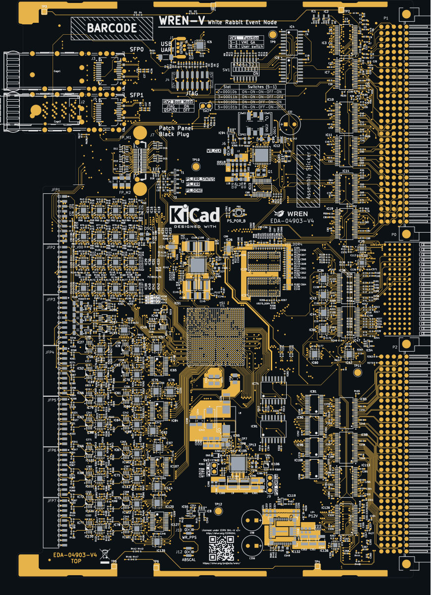
WREN V (OHWR0093 R4) is an open-hardware circuit board from its public repository, designed in KiCad EDA: a 12-layer board of 160 × 233.4 mm with 1429 components and 1726 nets, published under CERN-OHL-W-2.0.
review 94% walked · 13 findings: 1 blocker · 8 major · 4 minor (125 items)
Open in the interactive viewerRead the full review
Design review
Probe recorded 13 findings: 1 blocker · 8 major · 4 minor (125 items) on this design. Each is shown here with its reasoning; the full review links every one to the pins, nets and datasheet pages it rests on.
- PowerGroundShortblockerOpen
'GND' carries a power pin (IC105.32) and a ground pin (IC143.8)
Net 'GND' connects a power pin (IC105.32) and a ground pin (IC143.8).
At GND
IC10 (VME AM/AS*/WRITE* transceiver) has no pull on OE or DIR; with PUDC_B high its B-port can drive the VME backplane before the FPGA is configured
IC10 (SN74VMEH22501) drives VME AM0-AM5, AS\* and WRITE\* onto the backplane, but its OE and DIR come only from FPGA pins with no pull resistor, and PUDC_B is strapped high, so those pins float until the FPGA is configured: in that window IC10 can enable its B-port and drive address-strobe and address-modifier lines on a live VME crate.
The control pins are undefined until configuration
Quantity Value Source IC10 OE (pin 14) /F_VME.AS_OE_N: IC51 ball AH10 (bank 43) and nothing else netlist IC10 DIR (pin 24) /F_VME.AS_N_DIR: IC51 ball F12 (bank 45) and nothing else netlist PUDC_B (IC51 ball U7) pulled to P1V8 by R497 1k, i.e. high netlist PUDC_B = 1 "Weak preconfiguration I/O pull-up resistors disabled" UG1075 v1.13, Table 1-4, p23 VMEH22501 OE "When OE is low, all 3A- or 3B-port outputs are active" SN74VMEH22501 SCES357F, p4 IC10 3B port VMEPX.AM0-AM5, VMEPX.AS_N, VMEPX.WRITE_N (to P1) netlist With the PL I/O 3-stated and unpulled from power-up until the bitstream loads (or forever, if the FPGA never configures), OE and DIR float. A floating OE that reads low, with DIR high (3A to 3B), turns on IC10's VME-side drivers. The 3A inputs have bus hold (SCES357F p1), so they drive whatever level they hold onto AS\*, AM and WRITE\*. The VMEH22501's power-up 3-state (p2) only covers the supply ramp, not the configuration time.
Every other VME transceiver on the board is strapped
``
mermaid graph LR FPGA[IC51 bank 43/45, unconfigured: Hi-Z, no pull-up as PUDC_B=1] -- AS_OE_N --> OE[IC10 OE: no pull] FPGA -- AS_N_DIR --> DIR[IC10 DIR: no pull] OE --> IC10[IC10 SN74VMEH22501] -- AS*, AM0-5, WRITE* --> P1[VME P1 backplane]``Transceiver group OE strap DIR strap IC11, IC14, IC19, IC113 (A bus) R52 10k to P3V3 (disabled) R399 10k to GND (receive) IC137, IC139, IC141, IC142 (D bus) via IC2 from F_VME.D_OE_N, R5 10k to P1V8 (disabled) R685 10k to GND (receive) IC10 (AM, AS\*, WRITE\*) none none The designer's own pattern holds the backplane drivers off and in receive until the FPGA takes over. IC10 is the one group left out. Adding a pull-up on /F_VME.AS_OE_N (to P3V3, as R52) and a pull-down on /F_VME.AS_N_DIR (as R399) would close it.
- concernCON-001majorOpen
P2 D26/D27, D29/D30 (TTC_DATA1, TTC_DATA2) to WREN V BST RTM RP2
Both TTC data pairs reach the WREN V BST RTM with P and N swapped, so every TTC data bit arrives at the RTM's fanout buffers inverted. Is the inversion intended (e.g. tolerated by biphase-mark coding, or undone in gateware)?
The two ends of each pair
Pair WREN V driver pin WREN V P2 contact RTM RP2 contact RTM receiver pin TTC_DATA1 IC136 (LMK1D2102) pin 9 = OUT0_P D27 D27 = DATA1_N IC1 (SY58031U) pin 6 = /IN TTC_DATA1 IC136 pin 10 = OUT0_N D26 D26 = DATA1_P IC1 pin 3 = IN TTC_DATA2 IC136 pin 13 = OUT2_P D30 D30 = DATA2_N IC12 (SY58031U) pin 6 = /IN TTC_DATA2 IC136 pin 14 = OUT2_N D29 D29 = DATA2_P IC12 pin 3 = IN Sources: LMK1D2102 datasheet p4, pin functions ("OUT0_P, OUT0_N 9, 10 ... OUT2_P, OUT2_N 13, 14 ... Differential LVDS output pair"); SY58031U datasheet p3, pin description ("3, 6 IN, /IN Differential signal input"). Netlists: WREN V (EDA-04903-V4-0) nets TTC_DATA1_P/N, TTC_DATA2_P/N; RTM (EDA-04996-V2-0) nets DATA1_P/N, DATA2_P/N. P2 meets RP2 pin for pin through the VME64x backplane, a seam the copper on both sides corroborates. Every other differential pair on this seam (BUNCHCLK1/2, TURNCLK1/2) keeps its polarity: D14/D15, D17/D18, D20/D21 and D23/D24 run P to P.
``
mermaid flowchart LR A["IC136 OUT0_P (pin 9)"] -->|P2/RP2 D27| B["IC1 /IN (pin 6)"] C["IC136 OUT0_N (pin 10)"] -->|P2/RP2 D26| D["IC1 IN (pin 3)"]``Why it may be harmless
If the TTC/BST data is biphase-mark encoded, the inversion does not change the decoded data. If the FPGA can invert IC136's input, the gateware may already undo it. Neither is stated on the sheets, so this is a question for the designers, not a defect claim.
- BomLayoutMismatchmajorOpen
BomLayoutMismatch: 6 components×6
Checked by the review, stands · Claude walker V1 (Cern session) — HS1 (heatsink), TT1 (thermal item) and NUT1-NUT4 are mechanical BOM-only lines in CERN's assembly BOM with no footprint by design (the brief for this round notes HS1/TT1 as BOM-only). The finding is factually right (no placement) and harmless; left for the owner.
At HS1, NUT1, NUT2, NUT3, NUT4, TT1
Each finding, with its own headline
- HS1BOM refdes 'HS1' is not placed in the layout.
- NUT1BOM refdes 'NUT1' is not placed in the layout.
- NUT2BOM refdes 'NUT2' is not placed in the layout.
- NUT3BOM refdes 'NUT3' is not placed in the layout.
- NUT4BOM refdes 'NUT4' is not placed in the layout.
- TT1BOM refdes 'TT1' is not placed in the layout.
- EsdProtectorPlacementmajorOpen
EsdProtectorPlacement: 43 components×43
Checked by the review, stands · Claude walker V1 (Cern session) — Measured by Probe (esdPlacement): PRTR5V0U4D stubs of 1.2-17.9 mm on the J7 Patch Panel lines, some with 1-2 vias before the clamp; 0402ESDA stubs ~1.2 mm on J4. The makers' guidance is qualitative (Nexperia PRTR5V0U2X p6 'as close to the input terminal or connector as possible'; Eaton 0402ESDA p2 'as close to the signal input as possible', '0-stub pad design'); the PRTR5V0U4D sheet gives no figure. Layout heuristic, not a datasheet requirement: no datasheet or app note on file sets a limit for this board (Probe's thresholds are its defaults). Examined, left open for the owner.
At D10, D11, D12, D13, D14, D15 and 7 more
Each finding, with its own headline
D10D10.1 on '/PP_OUT11': D10.1 hangs 6.73 mm off the line (limit 1 mm, default
D10 (PRTR5V0U4D) protects '/PP_OUT11' at J7.20. Along the copper: 7.87 mm of track from the contact, 0 via(s) before it, on a 6.73 mm branch off the line; the line runs 83.76 mm on to R195.2; D10 sits 1.6 mm farther from the contact than the nearest place outside J7.
D10.1 hangs 6.73 mm off the line (limit 1 mm, default: no datasheet figure on file): the line carries the strike past it while the clamp is reached through the branch.
Measured on the copper the ODB states: tracks, the pads they land on, and the netlist's vias. Not a straight line between centroids.
D10D10.3 on '/PP_OUT8': 2 via(s) between J7.23 and D10.3
D10 (PRTR5V0U4D) protects '/PP_OUT8' at J7.23. Along the copper: 14.49 mm of track from the contact, 2 via(s) before it, on a 12.4 mm branch off the line; the line runs 55.63 mm on to R179.2; D10 sits 5.3 mm farther from the contact than the nearest place outside J7.
2 via(s) between J7.23 and D10.3: the strike reaches an inner layer before it is clamped. D10.3 hangs 12.4 mm off the line (limit 1 mm, default: no datasheet figure on file): the line carries the strike past it while the clamp is reached through the branch.
Measured on the copper the ODB states: tracks, the pads they land on, and the netlist's vias. Not a straight line between centroids.
D10D10.4 on '/PP_OUT9': D10.4 hangs 2.52 mm off the line (limit 1 mm, default
D10 (PRTR5V0U4D) protects '/PP_OUT9' at J7.24. Along the copper: 3.67 mm of track from the contact, 0 via(s) before it, on a 2.52 mm branch off the line; the line runs 88.59 mm on to R197.2; D10 sits 1.6 mm farther from the contact than the nearest place outside J7.
D10.4 hangs 2.52 mm off the line (limit 1 mm, default: no datasheet figure on file): the line carries the strike past it while the clamp is reached through the branch.
Measured on the copper the ODB states: tracks, the pads they land on, and the netlist's vias. Not a straight line between centroids.
D10D10.6 on '/PP_OUT10': D10.6 hangs 3.39 mm off the line (limit 1 mm, default
D10 (PRTR5V0U4D) protects '/PP_OUT10' at J7.22. Along the copper: 4.81 mm of track from the contact, 0 via(s) before it, on a 3.39 mm branch off the line; the line runs 56.48 mm on to R177.2; D10 sits 1.6 mm farther from the contact than the nearest place outside J7.
D10.6 hangs 3.39 mm off the line (limit 1 mm, default: no datasheet figure on file): the line carries the strike past it while the clamp is reached through the branch.
Measured on the copper the ODB states: tracks, the pads they land on, and the netlist's vias. Not a straight line between centroids.
D11D11.1 on '/PP_OUT19': D11.1 hangs 6.63 mm off the line (limit 1 mm, default
D11 (PRTR5V0U4D) protects '/PP_OUT19' at J7.4. Along the copper: 7.75 mm of track from the contact, 0 via(s) before it, on a 6.63 mm branch off the line; the line runs 37.49 mm on to R63.2; D11 sits 1.6 mm farther from the contact than the nearest place outside J7.
D11.1 hangs 6.63 mm off the line (limit 1 mm, default: no datasheet figure on file): the line carries the strike past it while the clamp is reached through the branch.
Measured on the copper the ODB states: tracks, the pads they land on, and the netlist's vias. Not a straight line between centroids.
D11D11.3 on '/PP_OUT16': D11.3 hangs 4.69 mm off the line (limit 1 mm, default
D11 (PRTR5V0U4D) protects '/PP_OUT16' at J7.10. Along the copper: 6.44 mm of track from the contact, 0 via(s) before it, on a 4.69 mm branch off the line; the line runs 23.47 mm on to R42.2; D11 sits 1.6 mm farther from the contact than the nearest place outside J7.
D11.3 hangs 4.69 mm off the line (limit 1 mm, default: no datasheet figure on file): the line carries the strike past it while the clamp is reached through the branch.
Measured on the copper the ODB states: tracks, the pads they land on, and the netlist's vias. Not a straight line between centroids.
D11D11.4 on '/PP_OUT17': D11.4 hangs 2.52 mm off the line (limit 1 mm, default
D11 (PRTR5V0U4D) protects '/PP_OUT17' at J7.8. Along the copper: 3.66 mm of track from the contact, 0 via(s) before it, on a 2.52 mm branch off the line; the line runs 30.57 mm on to R65.2; D11 sits 1.6 mm farther from the contact than the nearest place outside J7.
D11.4 hangs 2.52 mm off the line (limit 1 mm, default: no datasheet figure on file): the line carries the strike past it while the clamp is reached through the branch.
Measured on the copper the ODB states: tracks, the pads they land on, and the netlist's vias. Not a straight line between centroids.
D11D11.6 on '/PP_OUT18': D11.6 hangs 3.29 mm off the line (limit 1 mm, default
D11 (PRTR5V0U4D) protects '/PP_OUT18' at J7.6. Along the copper: 4.73 mm of track from the contact, 0 via(s) before it, on a 3.29 mm branch off the line; the line runs 28.16 mm on to R48.2; D11 sits 1.6 mm farther from the contact than the nearest place outside J7.
D11.6 hangs 3.29 mm off the line (limit 1 mm, default: no datasheet figure on file): the line carries the strike past it while the clamp is reached through the branch.
Measured on the copper the ODB states: tracks, the pads they land on, and the netlist's vias. Not a straight line between centroids.
D12D12.1 on '/PP_OUT27': 1 via(s) between J7.9 and D12.1
D12 (PRTR5V0U4D) protects '/PP_OUT27' at J7.9. Along the copper: 8.59 mm of track from the contact, 1 via(s) before it, on a 6.97 mm branch off the line; the line runs 83.1 mm on to R150.2; D12 sits 2.17 mm farther from the contact than the nearest place outside J7.
1 via(s) between J7.9 and D12.1: the strike reaches an inner layer before it is clamped. D12.1 hangs 6.97 mm off the line (limit 1 mm, default: no datasheet figure on file): the line carries the strike past it while the clamp is reached through the branch.
Measured on the copper the ODB states: tracks, the pads they land on, and the netlist's vias. Not a straight line between centroids.
D12D12.3 on '/PP_OUT24': 1 via(s) between J7.15 and D12.3
D12 (PRTR5V0U4D) protects '/PP_OUT24' at J7.15. Along the copper: 7.22 mm of track from the contact, 1 via(s) before it, on a 6 mm branch off the line; the line runs 44.95 mm on to R125.2; D12 sits 2.23 mm farther from the contact than the nearest place outside J7.
1 via(s) between J7.15 and D12.3: the strike reaches an inner layer before it is clamped. D12.3 hangs 6 mm off the line (limit 1 mm, default: no datasheet figure on file): the line carries the strike past it while the clamp is reached through the branch.
Measured on the copper the ODB states: tracks, the pads they land on, and the netlist's vias. Not a straight line between centroids.
D12D12.4 on '/PP_OUT25': 1 via(s) between J7.13 and D12.4
D12 (PRTR5V0U4D) protects '/PP_OUT25' at J7.13. Along the copper: 4.41 mm of track from the contact, 1 via(s) before it, on a 2.79 mm branch off the line; the line runs 54.04 mm on to R152.2; D12 sits 2.17 mm farther from the contact than the nearest place outside J7.
1 via(s) between J7.13 and D12.4: the strike reaches an inner layer before it is clamped. D12.4 hangs 2.79 mm off the line (limit 1 mm, default: no datasheet figure on file): the line carries the strike past it while the clamp is reached through the branch.
Measured on the copper the ODB states: tracks, the pads they land on, and the netlist's vias. Not a straight line between centroids.
D12D12.6 on '/PP_OUT26': 1 via(s) between J7.11 and D12.6
D12 (PRTR5V0U4D) protects '/PP_OUT26' at J7.11. Along the copper: 5.48 mm of track from the contact, 1 via(s) before it, on a 4.26 mm branch off the line; the line runs 67.49 mm on to R123.2; D12 sits 2.17 mm farther from the contact than the nearest place outside J7.
1 via(s) between J7.11 and D12.6: the strike reaches an inner layer before it is clamped. D12.6 hangs 4.26 mm off the line (limit 1 mm, default: no datasheet figure on file): the line carries the strike past it while the clamp is reached through the branch.
Measured on the copper the ODB states: tracks, the pads they land on, and the netlist's vias. Not a straight line between centroids.
D13D13.1 on '/PP_OUT6': 1 via(s) between J7.27 and D13.1
D13 (PRTR5V0U4D) protects '/PP_OUT6' at J7.27. Along the copper: 8.78 mm of track from the contact, 1 via(s) before it, on a 7.51 mm branch off the line; the line runs 46.91 mm on to R76.2; D13 sits 2.17 mm farther from the contact than the nearest place outside J7.
1 via(s) between J7.27 and D13.1: the strike reaches an inner layer before it is clamped. D13.1 hangs 7.51 mm off the line (limit 1 mm, default: no datasheet figure on file): the line carries the strike past it while the clamp is reached through the branch.
Measured on the copper the ODB states: tracks, the pads they land on, and the netlist's vias. Not a straight line between centroids.
D13D13.3 on '/PP_OUT5': 1 via(s) between J7.29 and D13.3
D13 (PRTR5V0U4D) protects '/PP_OUT5' at J7.29. Along the copper: 7.45 mm of track from the contact, 1 via(s) before it, on a 4.81 mm branch off the line; the line runs 47.78 mm on to R86.2; D13 sits 2.17 mm farther from the contact than the nearest place outside J7.
1 via(s) between J7.29 and D13.3: the strike reaches an inner layer before it is clamped. D13.3 hangs 4.81 mm off the line (limit 1 mm, default: no datasheet figure on file): the line carries the strike past it while the clamp is reached through the branch.
Measured on the copper the ODB states: tracks, the pads they land on, and the netlist's vias. Not a straight line between centroids.
D13D13.4 on '/PP_OUT4': 1 via(s) between J7.31 and D13.4
D13 (PRTR5V0U4D) protects '/PP_OUT4' at J7.31. Along the copper: 4.35 mm of track from the contact, 1 via(s) before it, on a 2.76 mm branch off the line; the line runs 40.2 mm on to R78.2; D13 sits 2.17 mm farther from the contact than the nearest place outside J7.
1 via(s) between J7.31 and D13.4: the strike reaches an inner layer before it is clamped. D13.4 hangs 2.76 mm off the line (limit 1 mm, default: no datasheet figure on file): the line carries the strike past it while the clamp is reached through the branch.
Measured on the copper the ODB states: tracks, the pads they land on, and the netlist's vias. Not a straight line between centroids.
D13D13.6 on '/PP_OUT7': 1 via(s) between J7.25 and D13.6
D13 (PRTR5V0U4D) protects '/PP_OUT7' at J7.25. Along the copper: 4.16 mm of track from the contact, 1 via(s) before it, on a 2.76 mm branch off the line; the line runs 55.25 mm on to R84.2; D13 sits 2.17 mm farther from the contact than the nearest place outside J7.
1 via(s) between J7.25 and D13.6: the strike reaches an inner layer before it is clamped. D13.6 hangs 2.76 mm off the line (limit 1 mm, default: no datasheet figure on file): the line carries the strike past it while the clamp is reached through the branch.
Measured on the copper the ODB states: tracks, the pads they land on, and the netlist's vias. Not a straight line between centroids.
D14D14.1 on '/PP_OUT14': 1 via(s) between J7.14 and D14.1
D14 (PRTR5V0U4D) protects '/PP_OUT14' at J7.14. Along the copper: 4.53 mm of track from the contact, 1 via(s) before it, on a 3.06 mm branch off the line; the line runs 62.11 mm on to R173.2; D14 sits 1.6 mm farther from the contact than the nearest place outside J7.
1 via(s) between J7.14 and D14.1: the strike reaches an inner layer before it is clamped. D14.1 hangs 3.06 mm off the line (limit 1 mm, default: no datasheet figure on file): the line carries the strike past it while the clamp is reached through the branch.
Measured on the copper the ODB states: tracks, the pads they land on, and the netlist's vias. Not a straight line between centroids.
D14D14.3 on '/PP_OUT13': 1 via(s) between J7.16 and D14.3
D14 (PRTR5V0U4D) protects '/PP_OUT13' at J7.16. Along the copper: 3.63 mm of track from the contact, 1 via(s) before it, on a 2.49 mm branch off the line; the line runs 81.3 mm on to R193.2; D14 sits 1.6 mm farther from the contact than the nearest place outside J7.
1 via(s) between J7.16 and D14.3: the strike reaches an inner layer before it is clamped. D14.3 hangs 2.49 mm off the line (limit 1 mm, default: no datasheet figure on file): the line carries the strike past it while the clamp is reached through the branch.
Measured on the copper the ODB states: tracks, the pads they land on, and the netlist's vias. Not a straight line between centroids.
D14D14.4 on '/PP_OUT12': 1 via(s) between J7.18 and D14.4
D14 (PRTR5V0U4D) protects '/PP_OUT12' at J7.18. Along the copper: 6.63 mm of track from the contact, 1 via(s) before it, on a 5.23 mm branch off the line; the line runs 57.59 mm on to R175.2; D14 sits 1.6 mm farther from the contact than the nearest place outside J7.
1 via(s) between J7.18 and D14.4: the strike reaches an inner layer before it is clamped. D14.4 hangs 5.23 mm off the line (limit 1 mm, default: no datasheet figure on file): the line carries the strike past it while the clamp is reached through the branch.
Measured on the copper the ODB states: tracks, the pads they land on, and the netlist's vias. Not a straight line between centroids.
D14D14.6 on '/PP_OUT15': 1 via(s) between J7.12 and D14.6
D14 (PRTR5V0U4D) protects '/PP_OUT15' at J7.12. Along the copper: 7.59 mm of track from the contact, 1 via(s) before it, on a 6.45 mm branch off the line; the line runs 75.84 mm on to R191.2; D14 sits 1.6 mm farther from the contact than the nearest place outside J7.
1 via(s) between J7.12 and D14.6: the strike reaches an inner layer before it is clamped. D14.6 hangs 6.45 mm off the line (limit 1 mm, default: no datasheet figure on file): the line carries the strike past it while the clamp is reached through the branch.
Measured on the copper the ODB states: tracks, the pads they land on, and the netlist's vias. Not a straight line between centroids.
D15D15.1 on '/PP_OUT22': D15.1 hangs 3.41 mm off the line (limit 1 mm, default
D15 (PRTR5V0U4D) protects '/PP_OUT22' at J7.19. Along the copper: 4.68 mm of track from the contact, 0 via(s) before it, on a 3.41 mm branch off the line; the line runs 35.72 mm on to R39.2; D15 sits 2.17 mm farther from the contact than the nearest place outside J7.
D15.1 hangs 3.41 mm off the line (limit 1 mm, default: no datasheet figure on file): the line carries the strike past it while the clamp is reached through the branch.
Measured on the copper the ODB states: tracks, the pads they land on, and the netlist's vias. Not a straight line between centroids.
D15D15.3 on '/PP_OUT21': D15.3 hangs 1.42 mm off the line (limit 1 mm, default
D15 (PRTR5V0U4D) protects '/PP_OUT21' at J7.21. Along the copper: 4.06 mm of track from the contact, 0 via(s) before it, on a 1.42 mm branch off the line; the line runs 44.58 mm on to R61.2; D15 sits 2.17 mm farther from the contact than the nearest place outside J7.
D15.3 hangs 1.42 mm off the line (limit 1 mm, default: no datasheet figure on file): the line carries the strike past it while the clamp is reached through the branch.
Measured on the copper the ODB states: tracks, the pads they land on, and the netlist's vias. Not a straight line between centroids.
D15D15.4 on '/PP_OUT20': 2 via(s) between J7.2 and D15.4
D15 (PRTR5V0U4D) protects '/PP_OUT20' at J7.2. Along the copper: 16.83 mm of track from the contact, 2 via(s) before it, on a 1.55 mm branch off the line; the line runs 51.66 mm on to R40.2; D15 sits 6.17 mm farther from the contact than the nearest place outside J7.
2 via(s) between J7.2 and D15.4: the strike reaches an inner layer before it is clamped. D15.4 hangs 1.55 mm off the line (limit 1 mm, default: no datasheet figure on file): the line carries the strike past it while the clamp is reached through the branch.
Measured on the copper the ODB states: tracks, the pads they land on, and the netlist's vias. Not a straight line between centroids.
D15D15.6 on '/PP_OUT23': D15.6 hangs 5.99 mm off the line (limit 1 mm, default
D15 (PRTR5V0U4D) protects '/PP_OUT23' at J7.17. Along the copper: 7.54 mm of track from the contact, 0 via(s) before it, on a 5.99 mm branch off the line; the line runs 38.1 mm on to R59.2; D15 sits 2.17 mm farther from the contact than the nearest place outside J7.
D15.6 hangs 5.99 mm off the line (limit 1 mm, default: no datasheet figure on file): the line carries the strike past it while the clamp is reached through the branch.
Measured on the copper the ODB states: tracks, the pads they land on, and the netlist's vias. Not a straight line between centroids.
D16D16.1 on '/PP_OUT30': D16.1 hangs 4.65 mm off the line (limit 1 mm, default
D16 (PRTR5V0U4D) protects '/PP_OUT30' at J7.3. Along the copper: 5.87 mm of track from the contact, 0 via(s) before it, on a 4.65 mm branch off the line; the line runs 60.67 mm on to R113.2; D16 sits 2.17 mm farther from the contact than the nearest place outside J7.
D16.1 hangs 4.65 mm off the line (limit 1 mm, default: no datasheet figure on file): the line carries the strike past it while the clamp is reached through the branch.
Measured on the copper the ODB states: tracks, the pads they land on, and the netlist's vias. Not a straight line between centroids.
D16D16.3 on '/PP_OUT29': D16.3 hangs 3.03 mm off the line (limit 1 mm, default
D16 (PRTR5V0U4D) protects '/PP_OUT29' at J7.5. Along the copper: 4.63 mm of track from the contact, 0 via(s) before it, on a 3.03 mm branch off the line; the line runs 77.75 mm on to R156.2; D16 sits 2.23 mm farther from the contact than the nearest place outside J7.
D16.3 hangs 3.03 mm off the line (limit 1 mm, default: no datasheet figure on file): the line carries the strike past it while the clamp is reached through the branch.
Measured on the copper the ODB states: tracks, the pads they land on, and the netlist's vias. Not a straight line between centroids.
D16D16.4 on '/PP_OUT28': D16.4 hangs 6.23 mm off the line (limit 1 mm, default
D16 (PRTR5V0U4D) protects '/PP_OUT28' at J7.7. Along the copper: 7.45 mm of track from the contact, 0 via(s) before it, on a 6.23 mm branch off the line; the line runs 64.09 mm on to R114.2; D16 sits 2.37 mm farther from the contact than the nearest place outside J7.
D16.4 hangs 6.23 mm off the line (limit 1 mm, default: no datasheet figure on file): the line carries the strike past it while the clamp is reached through the branch.
Measured on the copper the ODB states: tracks, the pads they land on, and the netlist's vias. Not a straight line between centroids.
D16D16.6 on '/PP_OUT31': D16.6 hangs 7.58 mm off the line (limit 1 mm, default
D16 (PRTR5V0U4D) protects '/PP_OUT31' at J7.1. Along the copper: 9.04 mm of track from the contact, 0 via(s) before it, on a 7.58 mm branch off the line; the line runs 73.62 mm on to R155.2; D16 sits 2.17 mm farther from the contact than the nearest place outside J7.
D16.6 hangs 7.58 mm off the line (limit 1 mm, default: no datasheet figure on file): the line carries the strike past it while the clamp is reached through the branch.
Measured on the copper the ODB states: tracks, the pads they land on, and the netlist's vias. Not a straight line between centroids.
D17D17.1 on '/pp_connector/PP_LED1_DATA': D17.1 hangs 6.97 mm off the line (limit 1 mm, default
D17 (PRTR5V0U4D) protects '/pp_connector/PP_LED1_DATA' at J7.34. Along the copper: 6.97 mm of track from the contact, 0 via(s) before it, on a 6.97 mm branch off the line; the line runs 73.02 mm on to R215.2; D17 sits 1.6 mm farther from the contact than the nearest place outside J7.
D17.1 hangs 6.97 mm off the line (limit 1 mm, default: no datasheet figure on file): the line carries the strike past it while the clamp is reached through the branch.
Measured on the copper the ODB states: tracks, the pads they land on, and the netlist's vias. Not a straight line between centroids.
D17D17.3 on '/PP_ID0': 2 via(s) between J7.35 and D17.3
D17 (PRTR5V0U4D) protects '/PP_ID0' at J7.35. Along the copper: 13.66 mm of track from the contact, 2 via(s) before it, on a 1.82 mm branch off the line; the line runs 12.54 mm on to R481.1; D17 sits 5.3 mm farther from the contact than the nearest place outside J7.
2 via(s) between J7.35 and D17.3: the strike reaches an inner layer before it is clamped. D17.3 hangs 1.82 mm off the line (limit 1 mm, default: no datasheet figure on file): the line carries the strike past it while the clamp is reached through the branch. D17 joins the line 11.84 mm from J7.35 on a 12.54 mm run to R481.1: nearer the far end than the contact, so the surge travels most of the line before it is clamped.
Measured on the copper the ODB states: tracks, the pads they land on, and the netlist's vias. Not a straight line between centroids.
D17D17.5 on '/pp_connector/PP_VDD': 2 via(s) between J7.38 and D17.5
D17 (PRTR5V0U4D) protects '/pp_connector/PP_VDD' at J7.38. Along the copper: 13.97 mm of track from the contact, 2 via(s) before it, on a 9.24 mm branch off the line; the line runs 4.73 mm on to C62.1; D17 sits 1.6 mm farther from the contact than the nearest place outside J7.
2 via(s) between J7.38 and D17.5: the strike reaches an inner layer before it is clamped. D17.5 hangs 9.24 mm off the line (limit 1 mm, default: no datasheet figure on file): the line carries the strike past it while the clamp is reached through the branch.
Measured on the copper the ODB states: tracks, the pads they land on, and the netlist's vias. Not a straight line between centroids.
D17D17.5 on '/pp_connector/PP_VDD': 2 via(s) between J7.39 and D17.5
D17 (PRTR5V0U4D) protects '/pp_connector/PP_VDD' at J7.39. Along the copper: 17.88 mm of track from the contact, 2 via(s) before it, on a 9.24 mm branch off the line; the line runs 8.64 mm on to C62.1; D17 sits 5.3 mm farther from the contact than the nearest place outside J7.
2 via(s) between J7.39 and D17.5: the strike reaches an inner layer before it is clamped. D17.5 hangs 9.24 mm off the line (limit 1 mm, default: no datasheet figure on file): the line carries the strike past it while the clamp is reached through the branch. D17 joins the line 8.64 mm from J7.39 on a 8.64 mm run to C62.1: nearer the far end than the contact, so the surge travels most of the line before it is clamped.
Measured on the copper the ODB states: tracks, the pads they land on, and the netlist's vias. Not a straight line between centroids.
D17D17.6 on '/pp_connector/PP_LED0_DATA': 2 via(s) between J7.33 and D17.6
D17 (PRTR5V0U4D) protects '/pp_connector/PP_LED0_DATA' at J7.33. Along the copper: 13.32 mm of track from the contact, 2 via(s) before it, on a 10.74 mm branch off the line; the line runs 72.78 mm on to R221.2; D17 sits 5.3 mm farther from the contact than the nearest place outside J7.
2 via(s) between J7.33 and D17.6: the strike reaches an inner layer before it is clamped. D17.6 hangs 10.74 mm off the line (limit 1 mm, default: no datasheet figure on file): the line carries the strike past it while the clamp is reached through the branch.
Measured on the copper the ODB states: tracks, the pads they land on, and the netlist's vias. Not a straight line between centroids.
D18D18.1 on '/PP_ID2': D18.1 hangs 1.17 mm off the line (limit 1 mm, default
D18 (PRTR5V0U4D) protects '/PP_ID2' at J7.37. Along the copper: 6.81 mm of track from the contact, 0 via(s) before it, on a 1.17 mm branch off the line; the line runs 31.07 mm on to R482.1; D18 sits 1.78 mm farther from the contact than the nearest place outside J7.
D18.1 hangs 1.17 mm off the line (limit 1 mm, default: no datasheet figure on file): the line carries the strike past it while the clamp is reached through the branch.
Measured on the copper the ODB states: tracks, the pads they land on, and the netlist's vias. Not a straight line between centroids.
D18D18.5 on '/pp_connector/PP_VDD': D18.5 hangs 9.43 mm off the line (limit 1 mm, default
D18 (PRTR5V0U4D) protects '/pp_connector/PP_VDD' at J7.38. Along the copper: 9.43 mm of track from the contact, 0 via(s) before it, on a 9.43 mm branch off the line; the line runs 4.73 mm on to C62.1; D18 sits 5.48 mm farther from the contact than the nearest place outside J7.
D18.5 hangs 9.43 mm off the line (limit 1 mm, default: no datasheet figure on file): the line carries the strike past it while the clamp is reached through the branch.
Measured on the copper the ODB states: tracks, the pads they land on, and the netlist's vias. Not a straight line between centroids.
D18D18.5 on '/pp_connector/PP_VDD': D18.5 hangs 5.53 mm off the line (limit 1 mm, default
D18 (PRTR5V0U4D) protects '/pp_connector/PP_VDD' at J7.39. Along the copper: 5.53 mm of track from the contact, 0 via(s) before it, on a 5.53 mm branch off the line; the line runs 8.64 mm on to C62.1; D18 sits 1.78 mm farther from the contact than the nearest place outside J7.
D18.5 hangs 5.53 mm off the line (limit 1 mm, default: no datasheet figure on file): the line carries the strike past it while the clamp is reached through the branch.
Measured on the copper the ODB states: tracks, the pads they land on, and the netlist's vias. Not a straight line between centroids.
D3D3.1 on '/fpga/fpga-config/JTAG_TDI': D3.1 hangs 1.2 mm off the line (limit 1 mm, default
D3 (0402ESDA-MLP) protects '/fpga/fpga-config/JTAG_TDI' at J4.10. Along the copper: 4.58 mm of track from the contact, 0 via(s) before it, on a 1.2 mm branch off the line; the line runs 3.38 mm on to R20.1; D3 sits at J4, within 0.89 mm of the nearest place outside it to the contact: the track to it is mostly the escape out of J4's own pins, which no placement shortens.
D3.1 hangs 1.2 mm off the line (limit 1 mm, default: no datasheet figure on file): the line carries the strike past it while the clamp is reached through the branch.
Measured on the copper the ODB states: tracks, the pads they land on, and the netlist's vias. Not a straight line between centroids.
D4D4.1 on '/fpga/fpga-config/JTAG_TDO': D4.1 hangs 1.17 mm off the line (limit 1 mm, default
D4 (0402ESDA-MLP) protects '/fpga/fpga-config/JTAG_TDO' at J4.8. Along the copper: 4.52 mm of track from the contact, 0 via(s) before it, on a 1.17 mm branch off the line; the line runs 3.35 mm on to R19.1; D4 sits at J4, within 0.91 mm of the nearest place outside it to the contact: the track to it is mostly the escape out of J4's own pins, which no placement shortens.
D4.1 hangs 1.17 mm off the line (limit 1 mm, default: no datasheet figure on file): the line carries the strike past it while the clamp is reached through the branch.
Measured on the copper the ODB states: tracks, the pads they land on, and the netlist's vias. Not a straight line between centroids.
D5D5.1 on '/fpga/fpga-config/PS_SRST_B': D5.1 hangs 1.23 mm off the line (limit 1 mm, default
D5 (0402ESDA-MLP) protects '/fpga/fpga-config/PS_SRST_B' at J4.14. Along the copper: 5.81 mm of track from the contact, 0 via(s) before it, on a 1.23 mm branch off the line; the line runs 4.59 mm on to R21.1; D5 sits 1.62 mm farther from the contact than the nearest place outside J4.
D5.1 hangs 1.23 mm off the line (limit 1 mm, default: no datasheet figure on file): the line carries the strike past it while the clamp is reached through the branch.
Measured on the copper the ODB states: tracks, the pads they land on, and the netlist's vias. Not a straight line between centroids.
D9D9.1 on '/PP_OUT3': 1 via(s) between J7.26 and D9.1
D9 (PRTR5V0U4D) protects '/PP_OUT3' at J7.26. Along the copper: 4.15 mm of track from the contact, 1 via(s) before it, the line runs through its pad (flow-through); the line runs 45.04 mm on to R88.2; D9 sits 1.6 mm farther from the contact than the nearest place outside J7.
1 via(s) between J7.26 and D9.1: the strike reaches an inner layer before it is clamped.
Measured on the copper the ODB states: tracks, the pads they land on, and the netlist's vias. Not a straight line between centroids.
D9D9.3 on '/PP_OUT0': 1 via(s) between J7.32 and D9.3
D9 (PRTR5V0U4D) protects '/PP_OUT0' at J7.32. Along the copper: 4.11 mm of track from the contact, 1 via(s) before it, on a 2.95 mm branch off the line; the line runs 26.32 mm on to R74.2; D9 sits 1.6 mm farther from the contact than the nearest place outside J7.
1 via(s) between J7.32 and D9.3: the strike reaches an inner layer before it is clamped. D9.3 hangs 2.95 mm off the line (limit 1 mm, default: no datasheet figure on file): the line carries the strike past it while the clamp is reached through the branch.
Measured on the copper the ODB states: tracks, the pads they land on, and the netlist's vias. Not a straight line between centroids.
D9D9.4 on '/PP_OUT1': 1 via(s) between J7.30 and D9.4
D9 (PRTR5V0U4D) protects '/PP_OUT1' at J7.30. Along the copper: 6.52 mm of track from the contact, 1 via(s) before it, on a 4.84 mm branch off the line; the line runs 36.54 mm on to R90.2; D9 sits 1.6 mm farther from the contact than the nearest place outside J7.
1 via(s) between J7.30 and D9.4: the strike reaches an inner layer before it is clamped. D9.4 hangs 4.84 mm off the line (limit 1 mm, default: no datasheet figure on file): the line carries the strike past it while the clamp is reached through the branch.
Measured on the copper the ODB states: tracks, the pads they land on, and the netlist's vias. Not a straight line between centroids.
D9D9.6 on '/PP_OUT2': 1 via(s) between J7.28 and D9.6
D9 (PRTR5V0U4D) protects '/PP_OUT2' at J7.28. Along the copper: 7.18 mm of track from the contact, 1 via(s) before it, on a 6.02 mm branch off the line; the line runs 29.45 mm on to R80.2; D9 sits 1.6 mm farther from the contact than the nearest place outside J7.
1 via(s) between J7.28 and D9.6: the strike reaches an inner layer before it is clamped. D9.6 hangs 6.02 mm off the line (limit 1 mm, default: no datasheet figure on file): the line carries the strike past it while the clamp is reached through the branch.
Measured on the copper the ODB states: tracks, the pads they land on, and the netlist's vias. Not a straight line between centroids.
- FloatingInputmajorOpen
FloatingInput: 17 nets×17
e.g. “IC12.2 on 'unconnected-(IC12-~{IN1}-Pad2)' has no driver and no pull” · 17 different statements
At unconnected-(IC12-FB_IN-Pad41), unconnected-(IC12-IN1-Pad1), unconnected-(IC12-IN2-Pad10), unconnected-(IC12-~{FB_IN}-Pad42), unconnected-(IC12-~{IN1}-Pad2), unconnected-(IC12-~{IN2}-Pad11) and 11 more
Each finding, with its own headline
unconnected-(IC12-FB_IN-Pad41)IC12.41 on 'unconnected-(IC12-FB_IN-Pad41)' has no driver and no pull
Net 'unconnected-(IC12-FB_IN-Pad41)': input(s) IC12.41 with no driver and no pull — floating input (undefined level); add a driver or a pull resistor.
unconnected-(IC12-IN1-Pad1)IC12.1 on 'unconnected-(IC12-IN1-Pad1)' has no driver and no pull
Net 'unconnected-(IC12-IN1-Pad1)': input(s) IC12.1 with no driver and no pull — floating input (undefined level); add a driver or a pull resistor.
unconnected-(IC12-IN2-Pad10)IC12.10 on 'unconnected-(IC12-IN2-Pad10)' has no driver and no pull
Net 'unconnected-(IC12-IN2-Pad10)': input(s) IC12.10 with no driver and no pull — floating input (undefined level); add a driver or a pull resistor.
unconnected-(IC12-~{FB_IN}-Pad42)IC12.42 on 'unconnected-(IC12-~{FB_IN}-Pad42)' has no driver and no pull
Net 'unconnected-(IC12-~{FB_IN}-Pad42)': input(s) IC12.42 with no driver and no pull — floating input (undefined level); add a driver or a pull resistor.
unconnected-(IC12-~{IN1}-Pad2)IC12.2 on 'unconnected-(IC12-~{IN1}-Pad2)' has no driver and no pull
Net 'unconnected-(IC12-~{IN1}-Pad2)': input(s) IC12.2 with no driver and no pull — floating input (undefined level); add a driver or a pull resistor.
unconnected-(IC12-~{IN2}-Pad11)IC12.11 on 'unconnected-(IC12-~{IN2}-Pad11)' has no driver and no pull
Net 'unconnected-(IC12-~{IN2}-Pad11)': input(s) IC12.11 with no driver and no pull — floating input (undefined level); add a driver or a pull resistor.
unconnected-(IC12-~{OE}-Pad12)IC12.12 on 'unconnected-(IC12-~{OE}-Pad12)' has no driver and no pull
Net 'unconnected-(IC12-~{OE}-Pad12)': input(s) IC12.12 with no driver and no pull — floating input (undefined level); add a driver or a pull resistor.
unconnected-(IC5-CTS_ECI-Pad10)IC5.10 on 'unconnected-(IC5-CTS_ECI-Pad10)' has no driver and no pull
Net 'unconnected-(IC5-CTS_ECI-Pad10)': input(s) IC5.10 with no driver and no pull — floating input (undefined level); add a driver or a pull resistor.
unconnected-(IC5-CTS_SCI-Pad18)IC5.18 on 'unconnected-(IC5-CTS_SCI-Pad18)' has no driver and no pull
Net 'unconnected-(IC5-CTS_SCI-Pad18)': input(s) IC5.18 with no driver and no pull — floating input (undefined level); add a driver or a pull resistor.
unconnected-(IC5-GPIO.0_SCI{slash}DCD_SCI-Pad24)IC5.24 on 'unconnected-(IC5-GPIO.0_SCI{slash}DCD_SCI-Pad24)' has no driver and no pull
Net 'unconnected-(IC5-GPIO.0_SCI{slash}DCD_SCI-Pad24)': input(s) IC5.24 with no driver and no pull — floating input (undefined level); add a driver or a pull resistor.
unconnected-(IC5-GPIO.1_ECI{slash}DSR_ECI-Pad14)IC5.14 on 'unconnected-(IC5-GPIO.1_ECI{slash}DSR_ECI-Pad14)' has no driver and no pull
Net 'unconnected-(IC5-GPIO.1_ECI{slash}DSR_ECI-Pad14)': input(s) IC5.14 with no driver and no pull — floating input (undefined level); add a driver or a pull resistor.
unconnected-(IC5-GPIO.2_SCI{slash}DSR_SCI-Pad22)IC5.22 on 'unconnected-(IC5-GPIO.2_SCI{slash}DSR_SCI-Pad22)' has no driver and no pull
Net 'unconnected-(IC5-GPIO.2_SCI{slash}DSR_SCI-Pad22)': input(s) IC5.22 with no driver and no pull — floating input (undefined level); add a driver or a pull resistor.
unconnected-(IC5-NC{slash}VPP{slash}DCD_ECI-Pad16)IC5.16 on 'unconnected-(IC5-NC{slash}VPP{slash}DCD_ECI-Pad16)' has no driver and no pull
Net 'unconnected-(IC5-NC{slash}VPP{slash}DCD_ECI-Pad16)': input(s) IC5.16 with no driver and no pull — floating input (undefined level); add a driver or a pull resistor.
unconnected-(IC5-~{SUSPEND}{slash}RI_ECI-Pad17)IC5.17 on 'unconnected-(IC5-~{SUSPEND}{slash}RI_ECI-Pad17)' has no driver and no pull
Net 'unconnected-(IC5-~{SUSPEND}{slash}RI_ECI-Pad17)': input(s) IC5.17 with no driver and no pull — floating input (undefined level); add a driver or a pull resistor.
unconnected-(IC5-~{SUSPEND}{slash}RI_SCI-Pad1)IC5.1 on 'unconnected-(IC5-~{SUSPEND}{slash}RI_SCI-Pad1)' has no driver and no pull
Net 'unconnected-(IC5-~{SUSPEND}{slash}RI_SCI-Pad1)': input(s) IC5.1 with no driver and no pull — floating input (undefined level); add a driver or a pull resistor.
unconnected-(IC74-~{RESET}-Pad3)IC74.3 on 'unconnected-(IC74-~{RESET}-Pad3)' has no driver and no pull
Net 'unconnected-(IC74-~{RESET}-Pad3)': input(s) IC74.3 with no driver and no pull — floating input (undefined level); add a driver or a pull resistor.
unconnected-(IC91-~{RESET}-Pad3)IC91.3 on 'unconnected-(IC91-~{RESET}-Pad3)' has no driver and no pull
Net 'unconnected-(IC91-~{RESET}-Pad3)': input(s) IC91.3 with no driver and no pull — floating input (undefined level); add a driver or a pull resistor.
- PartLifecyclemajorOpen
MT25QU512ABB8ESF-0SIT on 2 placements (IC74, IC91): the distributor catalogue reports "Obsolete" for Micron Technology Inc.'s MT25QU512ABB8ESF-0SIT
MT25QU512ABB8ESF-0SIT on 2 placements (IC74, IC91): the distributor catalogue reports "Obsolete" for Micron Technology Inc.'s MT25QU512ABB8ESF-0SIT — a sourcing/longevity risk to confirm against the MANUFACTURER before acting. That is the maker this board's BOM names (MICRON TECHNOLOGY). A distributor delisting is not the same claim as the part being unavailable; check the vendor's own lifecycle/product-change notice for the status and any named successor. Re-read the source: GET /api/odb/parts/MT25QU512ABB8ESF-0SIT/providers (which provider said it, the maker and part number it matched, its own words, and when we asked). THE LAST BUY DATE HAS PASSED (2026-08-31, 76 day(s) ago), so this is a substitution rather than a buy. The distributor reports NONE left. No approved alternate is recorded for this position.
At IC74
- ReferencePlaneDiscontinuitymajorOpen
ReferencePlaneDiscontinuity: 13 boards×13
Checked by the review, stands · Claude walker V1 (Cern session) — Layout heuristic, not a datasheet requirement: no datasheet or app note on file sets a limit for this board (Probe's thresholds are its defaults). Examined, left open for the owner. 135 findings: signal tracks crossing plane splits/voids or changing reference at vias; the stackup's reference planes are GND (L2, L4, L9, L11) with power planes between, so many are references changing between GND and power layers at vias. No signal-integrity requirement on file decides them.
At along@L11GND:GND|P0V85, along@L6PWR:MGT_1V8|P3V3, refchange:GND|P0V85, refchange:GND|P1V8, split@L11GND:GND|P0V85, void:GND@L11GND:160.32,-224.68 and 7 more
Each finding, with its own headline
along@L11GND:GND|P0V85'/fpga/F_I4' runs ALONG the split between the GND and P0V85 planes on L11GND at 1 place, the longest 3.25 mm; the impedance rises from 60 ohm to 68 ohm there at worst, 6 % of each edge reflected (fastest: /fpga/F_I4 at 100 ps 10-90 %, ASSUMED)
On L11GND the GND and P0V85 planes part, and '/fpga/F_I4' runs down the slot between them at 1 place(s), rather than across it. This is not a crossing: the return still follows the track, in the plane on its other side and in the slot's edges, so it does not detour. What changes is the track's own impedance. With the plane gone from under it on this side for that length, its field reaches further, to the slot's edges and to the next plane beyond, so its capacitance falls and its impedance rises; every edge travelling down it is partly reflected where it enters the stretch and again where it leaves, by (Z2 - Z1)/(Z2 + Z1). The longer the stretch against the edge's rise, the more of the edge sees the full step. A crossing is generally the worse fault; a mismatch is not free. Over solid plane each track is 60 ohm; along the slot 68 ohm, reflecting up to 6 % of each edge (a method-of-moments field solve of the cross-section, one dielectric; were the slot's edges to carry none of the return, up to 77 ohm). No place stays within 10 %, the tolerance controlled impedance is commonly built to (the stackup states none), so the finding is a warning. One decision covers the split line's slot: whether these tracks may run down it, or should be moved over solid plane.
- '/fpga/F_I4' on BOTTOM_LAYER at (142.15, -247.1), 3.71 mm, running ALONG the split for 3.25 mm, not across it, 60 ohm over solid plane, 68 ohm along it: 6 % of each edge reflected; other side: none: the signal layer is outermost
Every site is a row of this finding's evidence, keyed by net, layers and position. GET /api/odb/boards/98/reference-planes?group=along%40L11GND%3AGND%7CP0V85 serves each with its own layer_image region; all of them lie in x 140.99..143.15, y -249.89..-244.31 mm (board frame, Y up).
Read from the copper as drawn on the reference layer, along each track's centreline at exact breakpoints. The reference is the copper beside the track, never the layer's type or name. Whether it matters depends on each signal's edge rate, which nothing on file states for these nets: a slow static line crosses a split harmlessly, a fast edge does not.
along@L6PWR:MGT_1V8|P3V3'/WR_CLK.SPI_MOSI' runs ALONG the split between the MGT_1V8 and P3V3 planes on L6PWR at 1 place, the longest 1.06 mm; the impedance there is not said (fastest: /WR_CLK.SPI_MOSI at 1 ns 10-90 %, suggested by its name)
On L6PWR the MGT_1V8 and P3V3 planes part, and '/WR_CLK.SPI_MOSI' runs down the slot between them at 1 place(s), rather than across it. This is not a crossing: the return still follows the track, in the plane on its other side and in the slot's edges, so it does not detour. What changes is the track's own impedance. With the plane gone from under it on this side for that length, its field reaches further, to the slot's edges and to the next plane beyond, so its capacitance falls and its impedance rises; every edge travelling down it is partly reflected where it enters the stretch and again where it leaves, by (Z2 - Z1)/(Z2 + Z1). The longer the stretch against the edge's rise, the more of the edge sees the full step. A crossing is generally the worse fault; a mismatch is not free. At 1 place(s) the impedance cannot be said: the track's centreline is not over the slot. No place stays within 10 %, the tolerance controlled impedance is commonly built to (the stackup states none), so the finding is a warning. One decision covers the split line's slot: whether these tracks may run down it, or should be moved over solid plane.
- '/WR_CLK.SPI_MOSI' on L5 at (145.52, -214.32), 1.31 mm, running ALONG the split for 1.06 mm, not across it, impedance not said: the track's centreline is not over the slot; other side: GND on L4GND, 0.1 mm from the track against 0.12 mm to L6PWR: 45% of the return on L6PWR
Every site is a row of this finding's evidence, keyed by net, layers and position. GET /api/odb/boards/98/reference-planes?group=along%40L6PWR%3AMGT_1V8%7CP3V3 serves each with its own layer_image region; all of them lie in x 144.14..146.89, y -215.69..-212.69 mm (board frame, Y up).
Read from the copper as drawn on the reference layer, along each track's centreline at exact breakpoints. The reference is the copper beside the track, never the layer's type or name. Whether it matters depends on each signal's edge rate, which nothing on file states for these nets: a slow static line crosses a split harmlessly, a fast edge does not.
refchange:GND|P0V8529 nets change reference between GND and P0V85 at 30 vias; 10 of them partial (fastest: /F_PP_BP_IO.IO12 at 100 ps 10-90 %, ASSUMED)
At 30 via(s), on 29 net(s), the signal leaves a layer referenced by one of GND and P0V85 for a layer referenced by the other, and no plane references both layers. Different nets: no via can carry the return across; only decoupling between the two planes near the via can. The capacitor carrying the return across was measured at each via, at the knee of the crossing net's edge against 50 ohm assumed: 30 with none. 30 of them at an ASSUMED edge (no edge on file for the net): state one (net_timing_state) and it is re-read. One decision covers the pair: whether GND and P0V85 are decoupled to each other near these vias. A via whose layers have more references than these two is a site of each pair it joins. 10 of them are partial: another reference continues across through a stitching via of its net, so only part of the return has nowhere to go. The pure ones are listed first, then the partial ones with the farthest stitching via first.
- '/SFP0_SDA' at (142.35, -217.5), TOP_LAYER -> BOTTOM_LAYER: GND on L2GND to P0V85 on L11GND; pure, no reference continues across; stitching none, 110.8 mm of track past the via on BOTTOM_LAYER: At the 5 GHz knee of a 100 ps edge (10 ns 10-90 %, assumed: no edge is on file for the net) no capacitor carries the return; only the planes do. GND and P0V85 are not a thin pair (at most 0.2 mm), so their own capacitance does not carry the return. To serve it, change layers across the same plane, or move the signal to a layer referenced to ground. None.
- '/fpga/PS_UART_RXD' at (145.53, -216.67), TOP_LAYER -> BOTTOM_LAYER: GND on L2GND to P0V85 on L11GND; pure, no reference continues across; stitching none, 106.9 mm of track past the via on BOTTOM_LAYER: At the 5 GHz knee of a 100 ps edge (3 ns 10-90 %, assumed: no edge is on file for the net) no capacitor carries the return; only the planes do. GND and P0V85 are not a thin pair (at most 0.2 mm), so their own capacitance does not carry the return. To serve it, change layers across the same plane, or move the signal to a layer referenced to ground. None.
- '/fpga/PS_UART_TXD' at (144.73, -216.67), TOP_LAYER -> BOTTOM_LAYER: GND on L2GND to P0V85 on L11GND; pure, no reference continues across; stitching none, 99.9 mm of track past the via on BOTTOM_LAYER: At the 5 GHz knee of a 100 ps edge (3 ns 10-90 %, assumed: no edge is on file for the net) no capacitor carries the return; only the planes do. GND and P0V85 are not a thin pair (at most 0.2 mm), so their own capacitance does not carry the return. To serve it, change layers across the same plane, or move the signal to a layer referenced to ground. None.
- '/F_P0_P2.BUNCHCLK1' at (147.13, -223.07), L3 -> BOTTOM_LAYER: GND on L2GND, GND on L4GND to P0V85 on L11GND; pure, no reference continues across; stitching none, 95.8 mm of track past the via on BOTTOM_LAYER: At the 5 GHz knee of a 100 ps edge (1 ns 10-90 %, assumed: no edge is on file for the net) no capacitor carries the return; only the planes do. GND and P0V85 are not a thin pair (at most 0.2 mm), so their own capacitance does not carry the return. To serve it, change layers across the same plane, or move the signal to a layer referenced to ground. None.
- '/WR_CLK.SI5340_IRQ_N' at (143.13, -216.67), TOP_LAYER -> BOTTOM_LAYER: GND on L2GND to P0V85 on L11GND; pure, no reference continues across; stitching none, 79.4 mm of track past the via on BOTTOM_LAYER: At the 5 GHz knee of a 100 ps edge (1 ns 10-90 %, assumed: no edge is on file for the net) no capacitor carries the return; only the planes do. GND and P0V85 are not a thin pair (at most 0.2 mm), so their own capacitance does not carry the return. To serve it, change layers across the same plane, or move the signal to a layer referenced to ground. None.
- '/F_VME.BBSY_N_OE' at (145.53, -221.47), TOP_LAYER -> BOTTOM_LAYER: GND on L2GND to P0V85 on L11GND; pure, no reference continues across; stitching none, 76.1 mm of track past the via on BOTTOM_LAYER: At the 5 GHz knee of a 100 ps edge (100 ps 10-90 %, assumed: no edge is on file for the net) no capacitor carries the return; only the planes do. GND and P0V85 are not a thin pair (at most 0.2 mm), so their own capacitance does not carry the return. To serve it, change layers across the same plane, or move the signal to a layer referenced to ground. None.
- '/VME_SFP_SDA' at (147.13, -215.87), TOP_LAYER -> L10: GND on L2GND to GND on L9GND, P0V85 on L11GND; partial, GND continues through a via of GND 0.8 mm away; stitching none, 74.8 mm of track past the via on L10: At the 5 GHz knee of a 100 ps edge (10 ns 10-90 %, assumed: no edge is on file for the net) no capacitor carries the return; only the planes do. GND and P0V85 are not a thin pair (at most 0.2 mm), so their own capacitance does not carry the return. To serve it, change layers across the same plane, or move the signal to a layer referenced to ground. None.
- '/VME_SFP_SCL' at (147.93, -215.87), TOP_LAYER -> L10: GND on L2GND to GND on L9GND, P0V85 on L11GND; partial, GND continues through a via of GND 1.13 mm away; stitching none, 74.7 mm of track past the via on L10: At the 5 GHz knee of a 100 ps edge (10 ns 10-90 %, assumed: no edge is on file for the net) no capacitor carries the return; only the planes do. GND and P0V85 are not a thin pair (at most 0.2 mm), so their own capacitance does not carry the return. To serve it, change layers across the same plane, or move the signal to a layer referenced to ground. None.
- '/IOEXP.GPIO_Q' at (146.3, -221.5), TOP_LAYER -> L8: GND on L2GND to P1V8 on L7PWR, P0V85 on L9GND; pure, no reference continues across; stitching none, 69.2 mm of track past the via on L8: At the 5 GHz knee of a 100 ps edge (100 ps 10-90 %, assumed: no edge is on file for the net) no capacitor carries the return; only the planes do. GND and P0V85 are not a thin pair (at most 0.2 mm), so their own capacitance does not carry the return. To serve it, change layers across the same plane, or move the signal to a layer referenced to ground. None.
- '/I2C.SCL' at (147.93, -213.47), TOP_LAYER -> BOTTOM_LAYER: GND on L2GND to P0V85 on L11GND; pure, no reference continues across; stitching none, 59.7 mm of track past the via on BOTTOM_LAYER: At the 5 GHz knee of a 100 ps edge (10 ns 10-90 %, assumed: no edge is on file for the net) no capacitor carries the return; only the planes do. GND and P0V85 are not a thin pair (at most 0.2 mm), so their own capacitance does not carry the return. To serve it, change layers across the same plane, or move the signal to a layer referenced to ground. None.
- '/I2C.SDA' at (141.51, -243.3), L5 -> BOTTOM_LAYER: GND on L4GND, P3V3 on L6PWR to P0V85 on L11GND; pure, no reference continues across; stitching none, 59.6 mm of track past the via on BOTTOM_LAYER: At the 5 GHz knee of a 100 ps edge (10 ns 10-90 %, assumed: no edge is on file for the net) no capacitor carries the return; only the planes do. GND and P0V85 are not a thin pair (at most 0.2 mm), so their own capacitance does not carry the return. To serve it, change layers across the same plane, or move the signal to a layer referenced to ground. None.
- '/I2C.SDA' at (145.53, -212.67), TOP_LAYER -> BOTTOM_LAYER: GND on L2GND to P0V85 on L11GND; pure, no reference continues across; stitching none, 59.6 mm of track past the via on BOTTOM_LAYER: At the 5 GHz knee of a 100 ps edge (10 ns 10-90 %, assumed: no edge is on file for the net) no capacitor carries the return; only the planes do. GND and P0V85 are not a thin pair (at most 0.2 mm), so their own capacitance does not carry the return. To serve it, change layers across the same plane, or move the signal to a layer referenced to ground. None.
- and 18 more
Every site is a row of this finding's evidence, keyed by net, layers and position. GET /api/odb/boards/98/reference-planes?group=refchange%3AGND%7CP0V85 serves each with its own layer_image region; all of them lie in x 139.51..161.93, y -245.3..-210.67 mm (board frame, Y up).
The reference on each layer is the first plane the track meets leaving the via, anti-pads and the net's own copper skipped. Whether it matters depends on each signal's edge rate, which nothing on file states for these nets: a slow static line crosses a split harmlessly, a fast edge does not.
refchange:GND|P1V8197 nets change reference between GND and P1V8 at 491 vias; 490 of them partial (fastest: /DDR4-PS.A0 at 100 ps 10-90 %, ASSUMED)
At 491 via(s), on 197 net(s), the signal leaves a layer referenced by one of GND and P1V8 for a layer referenced by the other, and no plane references both layers. Different nets: no via can carry the return across; only decoupling between the two planes near the via can. The capacitor carrying the return across was measured at each via, at the knee of the crossing net's edge against 50 ohm assumed: 491 with none. 491 of them at an ASSUMED edge (no edge on file for the net): state one (net_timing_state) and it is re-read. One decision covers the pair: whether GND and P1V8 are decoupled to each other near these vias. A via whose layers have more references than these two is a site of each pair it joins. 490 of them are partial: another reference continues across through a stitching via of its net, so only part of the return has nowhere to go. The pure ones are listed first, then the partial ones with the farthest stitching via first.
- 'Net-(IC35-DATA)' at (151.38, -194.47), TOP_LAYER -> L8: GND on L2GND to P1V8 on L7PWR, GND on L9GND; partial, GND continues through a via of GND 2.74 mm away; stitching none, 286.4 mm of track past the via on L8: At the 5 GHz knee of a 100 ps edge (100 ps 10-90 %, assumed: no edge is on file for the net) no capacitor carries the return; only the planes do. GND and P1V8 are not a thin pair (at most 0.2 mm), so their own capacitance does not carry the return. To serve it, change layers across the same plane, or move the signal to a layer referenced to ground. None.
- 'Net-(IC35-CLK)' at (150.67, -195.07), TOP_LAYER -> L8: GND on L2GND to P1V8 on L7PWR, GND on L9GND; partial, GND continues through a via of GND 3.53 mm away; stitching none, 286.1 mm of track past the via on L8: At the 5 GHz knee of a 100 ps edge (1 ns 10-90 %, assumed: no edge is on file for the net) no capacitor carries the return; only the planes do. GND and P1V8 are not a thin pair (at most 0.2 mm), so their own capacitance does not carry the return. To serve it, change layers across the same plane, or move the signal to a layer referenced to ground. None.
- '/io_drivers_pp/bank1/OUT7' at (99.32, -201.02), TOP_LAYER -> L8: GND on L2GND to P1V8 on L7PWR, GND on L9GND; partial, GND continues through a via of GND 1.82 mm away; stitching none, 195.7 mm of track past the via on L8: At the 5 GHz knee of a 100 ps edge (100 ps 10-90 %, assumed: no edge is on file for the net) no capacitor carries the return; only the planes do. GND and P1V8 are not a thin pair (at most 0.2 mm), so their own capacitance does not carry the return. To serve it, change layers across the same plane, or move the signal to a layer referenced to ground. None.
- '/io_drivers_pp/bank1/OUT7' at (95.83, -200.74), TOP_LAYER -> L8: GND on L2GND to P1V8 on L7PWR, GND on L9GND; partial, GND continues through a via of GND 1.12 mm away; stitching none, 195.7 mm of track past the via on L8: At the 5 GHz knee of a 100 ps edge (100 ps 10-90 %, assumed: no edge is on file for the net) no capacitor carries the return; only the planes do. GND and P1V8 are not a thin pair (at most 0.2 mm), so their own capacitance does not carry the return. To serve it, change layers across the same plane, or move the signal to a layer referenced to ground. None.
- '/io_drivers_pp/bank1/OUT7' at (186.77, -256.41), TOP_LAYER -> L8: GND on L2GND to P1V8 on L7PWR, GND on L9GND; partial, GND continues through a via of GND 0.83 mm away; stitching none, 195.7 mm of track past the via on L8: At the 5 GHz knee of a 100 ps edge (100 ps 10-90 %, assumed: no edge is on file for the net) no capacitor carries the return; only the planes do. GND and P1V8 are not a thin pair (at most 0.2 mm), so their own capacitance does not carry the return. To serve it, change layers across the same plane, or move the signal to a layer referenced to ground. None.
- '/io_drivers_pp/bank1/OUT6' at (99.43, -196.94), TOP_LAYER -> L8: GND on L2GND to P1V8 on L7PWR, GND on L9GND; partial, GND continues through a via of GND 1.69 mm away; stitching none, 192.3 mm of track past the via on L8: At the 5 GHz knee of a 100 ps edge (100 ps 10-90 %, assumed: no edge is on file for the net) no capacitor carries the return; only the planes do. GND and P1V8 are not a thin pair (at most 0.2 mm), so their own capacitance does not carry the return. To serve it, change layers across the same plane, or move the signal to a layer referenced to ground. None.
- '/io_drivers_pp/bank1/OUT6' at (96.43, -196.04), TOP_LAYER -> L8: GND on L2GND to P1V8 on L7PWR, GND on L9GND; partial, GND continues through a via of GND 1.32 mm away; stitching none, 192.3 mm of track past the via on L8: At the 5 GHz knee of a 100 ps edge (100 ps 10-90 %, assumed: no edge is on file for the net) no capacitor carries the return; only the planes do. GND and P1V8 are not a thin pair (at most 0.2 mm), so their own capacitance does not carry the return. To serve it, change layers across the same plane, or move the signal to a layer referenced to ground. None.
- '/io_drivers_pp/bank1/OUT6' at (185.31, -255.47), TOP_LAYER -> L8: GND on L2GND to P1V8 on L7PWR, GND on L9GND; partial, GND continues through a via of GND 0.95 mm away; stitching none, 192.3 mm of track past the via on L8: At the 5 GHz knee of a 100 ps edge (100 ps 10-90 %, assumed: no edge is on file for the net) no capacitor carries the return; only the planes do. GND and P1V8 are not a thin pair (at most 0.2 mm), so their own capacitance does not carry the return. To serve it, change layers across the same plane, or move the signal to a layer referenced to ground. None.
- '/io_drivers_pp/bank1/OUT5' at (183.92, -254.95), TOP_LAYER -> L8: GND on L2GND to P1V8 on L7PWR, GND on L9GND; partial, GND continues through a via of GND 2.39 mm away; stitching none, 182.3 mm of track past the via on L8: At the 5 GHz knee of a 100 ps edge (100 ps 10-90 %, assumed: no edge is on file for the net) no capacitor carries the return; only the planes do. GND and P1V8 are not a thin pair (at most 0.2 mm), so their own capacitance does not carry the return. To serve it, change layers across the same plane, or move the signal to a layer referenced to ground. None.
- '/io_drivers_pp/bank1/OUT5' at (105.82, -201.02), TOP_LAYER -> L8: GND on L2GND to P1V8 on L7PWR, GND on L9GND; partial, GND continues through a via of GND 1.82 mm away; stitching none, 182.3 mm of track past the via on L8: At the 5 GHz knee of a 100 ps edge (100 ps 10-90 %, assumed: no edge is on file for the net) no capacitor carries the return; only the planes do. GND and P1V8 are not a thin pair (at most 0.2 mm), so their own capacitance does not carry the return. To serve it, change layers across the same plane, or move the signal to a layer referenced to ground. None.
- '/io_drivers_pp/bank1/OUT5' at (102.33, -200.74), TOP_LAYER -> L8: GND on L2GND to P1V8 on L7PWR, GND on L9GND; partial, GND continues through a via of GND 1.12 mm away; stitching none, 182.3 mm of track past the via on L8: At the 5 GHz knee of a 100 ps edge (100 ps 10-90 %, assumed: no edge is on file for the net) no capacitor carries the return; only the planes do. GND and P1V8 are not a thin pair (at most 0.2 mm), so their own capacitance does not carry the return. To serve it, change layers across the same plane, or move the signal to a layer referenced to ground. None.
- '/io_drivers_pp/bank1/OUT4' at (184.78, -253.92), TOP_LAYER -> L8: GND on L2GND to P1V8 on L7PWR, GND on L9GND; partial, GND continues through a via of GND 2.53 mm away; stitching none, 179.0 mm of track past the via on L8: At the 5 GHz knee of a 100 ps edge (100 ps 10-90 %, assumed: no edge is on file for the net) no capacitor carries the return; only the planes do. GND and P1V8 are not a thin pair (at most 0.2 mm), so their own capacitance does not carry the return. To serve it, change layers across the same plane, or move the signal to a layer referenced to ground. None.
- and 479 more
Every site is a row of this finding's evidence, keyed by net, layers and position. GET /api/odb/boards/98/reference-planes?group=refchange%3AGND%7CP1V8 serves each with its own layer_image region; all of them lie in x 92.96..220.47, y -303..-93.57 mm (board frame, Y up).
The reference on each layer is the first plane the track meets leaving the via, anti-pads and the net's own copper skipped. Whether it matters depends on each signal's edge rate, which nothing on file states for these nets: a slow static line crosses a split harmlessly, a fast edge does not.
split@L11GND:GND|P0V8540 nets cross the split between the GND and P0V85 planes on L11GND at 74 places; 11 with a plane on the track's other side (fastest: /F_PP_BP_IO.IO12 at 100 ps 10-90 %, ASSUMED)
On L11GND the GND and P0V85 planes part, and 40 nets cross from one to the other at 74 place(s). The return current cannot follow a track across; it detours to wherever the two planes are joined (a stitching capacitor, or the source), and the loop it opens radiates and couples. One decision covers the boundary: whether it is stitched near these crossings, or the nets crossing it are slow enough not to care. Tracks that run ALONG this split, down the slot rather than across it, are a finding of their own: theirs is an impedance step, not a detour. At 11 of the 74 crossing(s) the track's other neighbour carries a plane, which the return can use there; 63 are on an outer layer, with no other neighbour. 11 of the 74 crossing(s) have a plane on the track's other side at most twice as far away as the broken one (to first order each plane beside a stripline carries a share of the return inversely proportional to its distance from the track). The rest leave most or all of the return to the break, so the finding is a warning.
- '/DDR4-PS.RSTN' on BOTTOM_LAYER at (155.83, -212.27), 0.25 mm; other side: none: the signal layer is outermost
- '/DDR4-PS.RSTN' on BOTTOM_LAYER at (159.23, -212.27), 0.26 mm; other side: none: the signal layer is outermost
- '/F_P0_P2.BUNCHCLK1' on BOTTOM_LAYER at (142.12, -218), 0.26 mm; other side: none: the signal layer is outermost
- '/F_P0_P2.BUNCHCLK1' on BOTTOM_LAYER at (145.12, -219.13), 0.29 mm; other side: none: the signal layer is outermost
- '/F_P0_P2.BUNCHCLK1' on BOTTOM_LAYER at (146.74, -220.6), 0.29 mm; other side: none: the signal layer is outermost
- '/F_P0_P2.BUNCHCLK1' on BOTTOM_LAYER at (147.13, -221.06), 0.06 mm; other side: none: the signal layer is outermost
- '/F_P0_P2.BUNCHCLK2' on BOTTOM_LAYER at (142.12, -218.3), 0.26 mm; other side: none: the signal layer is outermost
- '/F_P0_P2.BUNCHCLK2' on BOTTOM_LAYER at (144.34, -219.14), 0.28 mm; other side: none: the signal layer is outermost
- '/F_P0_P2.BUNCHCLK2' on BOTTOM_LAYER at (145.14, -219.82), 0.29 mm; other side: none: the signal layer is outermost
- '/F_P0_P2.BUNCHCLK2' on BOTTOM_LAYER at (145.6, -220.26), 0.26 mm; other side: none: the signal layer is outermost
- '/F_P0_P2.BUNCHCLK2' on BOTTOM_LAYER at (145.94, -220.6), 0.27 mm; other side: none: the signal layer is outermost
- '/F_P0_P2.BUNCHCLK2' on BOTTOM_LAYER at (146.72, -223.16), 0.26 mm; other side: none: the signal layer is outermost
- and 62 more
Every site is a row of this finding's evidence, keyed by net, layers and position. GET /api/odb/boards/98/reference-planes?group=split%40L11GND%3AGND%7CP0V85 serves each with its own layer_image region; all of them lie in x 140.99..162.51, y -252.01..-210.74 mm (board frame, Y up).
Read from the copper as drawn on the reference layer, along each track's centreline at exact breakpoints. The reference is the copper beside the track, never the layer's type or name. Whether it matters depends on each signal's edge rate, which nothing on file states for these nets: a slow static line crosses a split harmlessly, a fast edge does not.
void:GND@L11GND:160.32,-224.68'/F_VME.D29' crosses where the outline of the GND plane on L11GND is drawn back, at 1 place, the longest 0.09 mm (fastest: /F_VME.D29 at 100 ps 10-90 %, ASSUMED)
Along '/F_VME.D29' on BOTTOM_LAYER, the GND plane on L11GND has 0.09 mm under the track with no copper, at (160.32, -224.68), the same plane on both sides. No single drill's anti-pad and no landing explains it: a clearance is excused only when it holds a drill and is drawn round it, or the track ends in it on the net's own pad or via, or runs through its own via's clearance and no farther. The return current detours round the void. No hole cleared it: the outline of the pour at x 71.48..230.48, y -315.17..-82.82 is drawn back there. One decision covers the void: whether these tracks may cross it, or the plane should be filled under them. No crossing has a plane on the track's other side, so the whole return meets the break.
- '/F_VME.D29' on BOTTOM_LAYER at (160.32, -224.68), 0.09 mm over no copper; other side: none: the signal layer is outermost
Every site is a row of this finding's evidence, keyed by net, layers and position. GET /api/odb/boards/98/reference-planes?group=void%3AGND%40L11GND%3A160.32%2C-224.68 serves each with its own layer_image region; all of them lie in x 159.32..161.32, y -225.72..-223.63 mm (board frame, Y up).
Read from the copper as drawn on the reference layer, along each track's centreline at exact breakpoints. The reference is the copper beside the track, never the layer's type or name. Whether it matters depends on each signal's edge rate, which nothing on file states for these nets: a slow static line crosses a split harmlessly, a fast edge does not.
void:GND@L2GND:120.17,-278.63'/io_drivers_fp/bank2/OUT6' crosses where the outline of the GND plane on L2GND and the GND plane on L4GND is drawn back, at 1 place, the longest 0.71 mm; 1 cleared on both sides of the track (fastest: /io_drivers_fp/bank2/OUT6 at 100 ps 10-90 %, ASSUMED)
Along '/io_drivers_fp/bank2/OUT6' on L3, the GND plane on L2GND has 0.71 mm under the track with no copper, at (120.17, -278.63), the same plane on both sides. No single drill's anti-pad and no landing explains it: a clearance is excused only when it holds a drill and is drawn round it, or the track ends in it on the net's own pad or via, or runs through its own via's clearance and no farther. The return current detours round the void. No hole cleared it: the outline of the pour at x 71.48..230.48, y -315.17..-82.82 is drawn back there. At 1 place(s) the track's plane is cleared on both sides of it, the same stretch on each reference layer: it has no plane on either side there, counted once. One decision covers the void: whether these tracks may cross it, or the plane should be filled under them. No crossing has a plane on the track's other side, so the whole return meets the break.
- one stretch, cleared on 2 reference layers: '/io_drivers_fp/bank2/OUT6' on L3 at (120.17, -278.63), 0.71 mm over no copper; other side: no plane on L4GND / '/io_drivers_fp/bank2/OUT6' on L3 at (120.17, -278.63), 0.71 mm over no copper; other side: no plane on L2GND
Every site is a row of this finding's evidence, keyed by net, layers and position. GET /api/odb/boards/98/reference-planes?group=void%3AGND%40L2GND%3A120.17%2C-278.63 serves each with its own layer_image region; all of them lie in x 118.82..121.17, y -279.81..-277.45 mm (board frame, Y up).
Read from the copper as drawn on the reference layer, along each track's centreline at exact breakpoints. The reference is the copper beside the track, never the layer's type or name. Whether it matters depends on each signal's edge rate, which nothing on file states for these nets: a slow static line crosses a split harmlessly, a fast edge does not.
void:GND@L2GND:207.67,-285.5'/F_VME.D_DIR' crosses where the outline of the GND plane on L2GND is drawn back, at 1 place, the longest 0.73 mm (fastest: /F_VME.D_DIR at 100 ps 10-90 %, ASSUMED)
Along '/F_VME.D_DIR' on TOP_LAYER, the GND plane on L2GND has 0.73 mm under the track with no copper, at (207.67, -285.5), the same plane on both sides. No single drill's anti-pad and no landing explains it: a clearance is excused only when it holds a drill and is drawn round it, or the track ends in it on the net's own pad or via, or runs through its own via's clearance and no farther. The return current detours round the void. No hole cleared it: the outline of the pour at x 71.48..230.48, y -315.17..-82.82 is drawn back there. One decision covers the void: whether these tracks may cross it, or the plane should be filled under them. No crossing has a plane on the track's other side, so the whole return meets the break.
- '/F_VME.D_DIR' on TOP_LAYER at (207.67, -285.5), 0.73 mm over no copper; other side: none: the signal layer is outermost
Every site is a row of this finding's evidence, keyed by net, layers and position. GET /api/odb/boards/98/reference-planes?group=void%3AGND%40L2GND%3A207.67%2C-285.5 serves each with its own layer_image region; all of them lie in x 206.67..208.74, y -287.02..-284.32 mm (board frame, Y up).
Read from the copper as drawn on the reference layer, along each track's centreline at exact breakpoints. The reference is the copper beside the track, never the layer's type or name. Whether it matters depends on each signal's edge rate, which nothing on file states for these nets: a slow static line crosses a split harmlessly, a fast edge does not.
void:GND@L4GND:145.12,-217.48'/F_VME.A22' crosses where the outline of the GND plane on L4GND and the MGT_1V8 plane on L6PWR is drawn back, at 1 place, the longest 0.09 mm; 1 cleared on both sides of the track (fastest: /F_VME.A22 at 100 ps 10-90 %, ASSUMED)
Along '/F_VME.A22' on L5, the GND plane on L4GND has 0.09 mm under the track with no copper, at (145.12, -217.48), the same plane on both sides. No single drill's anti-pad and no landing explains it: a clearance is excused only when it holds a drill and is drawn round it, or the track ends in it on the net's own pad or via, or runs through its own via's clearance and no farther. The return current detours round the void. No hole cleared it: the outline of the pour at x 136..155.5, y -227.4..-178.6 and of the pour at x 71.48..230.48, y -315.17..-82.82 is drawn back there. At 1 place(s) the track's plane is cleared on both sides of it, the same stretch on each reference layer: it has no plane on either side there, counted once. One decision covers the void: whether these tracks may cross it, or the plane should be filled under them. No crossing has a plane on the track's other side, so the whole return meets the break.
- one stretch, cleared on 2 reference layers: '/F_VME.A22' on L5 at (145.12, -217.48), 0.09 mm over no copper; other side: no plane on L6PWR / '/F_VME.A22' on L5 at (145.12, -217.48), 0.07 mm over no copper; other side: no plane on L4GND
Every site is a row of this finding's evidence, keyed by net, layers and position. GET /api/odb/boards/98/reference-planes?group=void%3AGND%40L4GND%3A145.12%2C-217.48 serves each with its own layer_image region; all of them lie in x 144.12..146.12, y -218.52..-216.43 mm (board frame, Y up).
Read from the copper as drawn on the reference layer, along each track's centreline at exact breakpoints. The reference is the copper beside the track, never the layer's type or name. Whether it matters depends on each signal's edge rate, which nothing on file states for these nets: a slow static line crosses a split harmlessly, a fast edge does not.
void:GND@L9GND:218.08,-267.97'/vme_interface/vme_p1_p2/LVDS_BUNCHCLK1_P' crosses where the outline of the P1V8 plane on L7PWR and the GND plane on L9GND is drawn back, at 1 place, the longest 0.2 mm; 1 cleared on both sides of the track (fastest: /vme_interface/vme_p1_p2/LVDS_BUNCHCLK1_P at 1 ns 10-90 %, suggested by its name)
Along '/vme_interface/vme_p1_p2/LVDS_BUNCHCLK1_P' on L8, the P1V8 plane on L7PWR has 0.2 mm under the track with no copper, at (218.08, -267.97), the same plane on both sides. No single drill's anti-pad and no landing explains it: a clearance is excused only when it holds a drill and is drawn round it, or the track ends in it on the net's own pad or via, or runs through its own via's clearance and no farther. The return current detours round the void. 2 of them run ALONG the bare copper, parallel to its edges, rather than across it (the longest 0.2 mm). No hole cleared it: the outline of the pour at x 71.48..230.48, y -315.17..-82.82 is drawn back there. At 1 place(s) the track's plane is cleared on both sides of it, the same stretch on each reference layer: it has no plane on either side there, counted once. One decision covers the void: whether these tracks may cross it, or the plane should be filled under them. No crossing has a plane on the track's other side, so the whole return meets the break.
- one stretch, cleared on 2 reference layers: '/vme_interface/vme_p1_p2/LVDS_BUNCHCLK1_P' on L8 at (218.08, -267.97), 0.2 mm, running ALONG the bare copper for 0.2 mm, not across it over no copper; other side: no plane on L9GND / '/vme_interface/vme_p1_p2/LVDS_BUNCHCLK1_P' on L8 at (218.08, -267.97), 0.2 mm, running ALONG the bare copper for 0.2 mm, not across it over no copper; other side: no plane on L7PWR
Every site is a row of this finding's evidence, keyed by net, layers and position. GET /api/odb/boards/98/reference-planes?group=void%3AGND%40L9GND%3A218.08%2C-267.97 serves each with its own layer_image region; all of them lie in x 216.98..219.18, y -268.97..-266.97 mm (board frame, Y up).
Read from the copper as drawn on the reference layer, along each track's centreline at exact breakpoints. The reference is the copper beside the track, never the layer's type or name. Whether it matters depends on each signal's edge rate, which nothing on file states for these nets: a slow static line crosses a split harmlessly, a fast edge does not.
void:P0V85@L11GND:148.34,-213.48'/fpga/PS_POR_B' crosses where the outline of the P0V85 plane on L11GND is drawn back, at 1 place, the longest 0.06 mm (fastest: /fpga/PS_POR_B at 100 ps 10-90 %, ASSUMED)
Along '/fpga/PS_POR_B' on BOTTOM_LAYER, the P0V85 plane on L11GND has 0.06 mm under the track with no copper, at (148.34, -213.48), the same plane on both sides. No single drill's anti-pad and no landing explains it: a clearance is excused only when it holds a drill and is drawn round it, or the track ends in it on the net's own pad or via, or runs through its own via's clearance and no farther. The return current detours round the void. No hole cleared it: the outline of the pour at x 142.25..161.25, y -250.75..-212 is drawn back there. One decision covers the void: whether these tracks may cross it, or the plane should be filled under them. No crossing has a plane on the track's other side, so the whole return meets the break.
- '/fpga/PS_POR_B' on BOTTOM_LAYER at (148.34, -213.48), 0.06 mm over no copper; other side: none: the signal layer is outermost
Every site is a row of this finding's evidence, keyed by net, layers and position. GET /api/odb/boards/98/reference-planes?group=void%3AP0V85%40L11GND%3A148.34%2C-213.48 serves each with its own layer_image region; all of them lie in x 147.34..149.34, y -214.5..-212.45 mm (board frame, Y up).
Read from the copper as drawn on the reference layer, along each track's centreline at exact breakpoints. The reference is the copper beside the track, never the layer's type or name. Whether it matters depends on each signal's edge rate, which nothing on file states for these nets: a slow static line crosses a split harmlessly, a fast edge does not.
void:P0V85@L11GND:148.73,-212.26'/fpga/fpga-config/PS_MODE0' crosses where the outline of the P0V85 plane on L11GND is drawn back, at 1 place, the longest 0.03 mm (fastest: /fpga/fpga-config/PS_MODE0 at 100 ps 10-90 %, ASSUMED)
Along '/fpga/fpga-config/PS_MODE0' on BOTTOM_LAYER, the P0V85 plane on L11GND has 0.03 mm under the track with no copper, at (148.73, -212.26), the same plane on both sides. No single drill's anti-pad and no landing explains it: a clearance is excused only when it holds a drill and is drawn round it, or the track ends in it on the net's own pad or via, or runs through its own via's clearance and no farther. The return current detours round the void. No hole cleared it: the outline of the pour at x 142.25..161.25, y -250.75..-212 is drawn back there. One decision covers the void: whether these tracks may cross it, or the plane should be filled under them. No crossing has a plane on the track's other side, so the whole return meets the break.
- '/fpga/fpga-config/PS_MODE0' on BOTTOM_LAYER at (148.73, -212.26), 0.03 mm over no copper; other side: none: the signal layer is outermost
Every site is a row of this finding's evidence, keyed by net, layers and position. GET /api/odb/boards/98/reference-planes?group=void%3AP0V85%40L11GND%3A148.73%2C-212.26 serves each with its own layer_image region; all of them lie in x 147.72..149.75, y -213.26..-211.26 mm (board frame, Y up).
Read from the copper as drawn on the reference layer, along each track's centreline at exact breakpoints. The reference is the copper beside the track, never the layer's type or name. Whether it matters depends on each signal's edge rate, which nothing on file states for these nets: a slow static line crosses a split harmlessly, a fast edge does not.
void:P0V85@L11GND:158.76,-228.59'Net-(IC51F-IO_T0U_N12_VRP_65)' crosses where the outline of the P0V85 plane on L11GND is drawn back, at 1 place, the longest 0.25 mm (fastest: Net-(IC51F-IO_T0U_N12_VRP_65) at 100 ps 10-90 %, ASSUMED)
Along 'Net-(IC51F-IO_T0U_N12_VRP_65)' on BOTTOM_LAYER, the P0V85 plane on L11GND has 0.25 mm under the track with no copper, at (158.76, -228.59), running to the end of the track. No single drill's anti-pad and no landing explains it: a clearance is excused only when it holds a drill and is drawn round it, or the track ends in it on the net's own pad or via, or runs through its own via's clearance and no farther. The return current detours round the void. No hole cleared it: the outline of the pour at x 142.25..161.25, y -250.75..-212 is drawn back there. One decision covers the void: whether these tracks may cross it, or the plane should be filled under them. No crossing has a plane on the track's other side, so the whole return meets the break.
- 'Net-(IC51F-IO_T0U_N12_VRP_65)' on BOTTOM_LAYER at (158.76, -228.59), 0.25 mm over no copper, to the end of the track; other side: none: the signal layer is outermost
Every site is a row of this finding's evidence, keyed by net, layers and position. GET /api/odb/boards/98/reference-planes?group=void%3AP0V85%40L11GND%3A158.76%2C-228.59 serves each with its own layer_image region; all of them lie in x 157.76..159.76, y -229.71..-227.46 mm (board frame, Y up).
Read from the copper as drawn on the reference layer, along each track's centreline at exact breakpoints. The reference is the copper beside the track, never the layer's type or name. Whether it matters depends on each signal's edge rate, which nothing on file states for these nets: a slow static line crosses a split harmlessly, a fast edge does not.
- SinglePointNetmajorOpen
SinglePointNet: 17 pins×17
e.g. “IC74.3 (RESET#) is an IC input left unconnected” · 16 different statements
At IC12.1, IC12.10, IC12.11, IC12.12, IC12.2, IC12.41 and 11 more
Each finding, with its own headline
IC12.1IC12.1 (IN1) is an IC input left unconnected
Pin IC12.1 (IN1) is an IC INPUT the designer flagged no-connect (KiCad net 'unconnected-(IC12-IN1-Pad1)'), but an input normally needs a defined level - confirm it is truly meant to float. If the datasheet defines this input left open (an internal pull, "read as low when left floating", or a tri-level input whose open state is one of its settings), file it on the pin as if_unused (pull_up, pull_down or may_float) with submit_pin_behavior, citing the page, and this finding clears.
IC12.10IC12.10 (IN2) is an IC input left unconnected
Pin IC12.10 (IN2) is an IC INPUT the designer flagged no-connect (KiCad net 'unconnected-(IC12-IN2-Pad10)'), but an input normally needs a defined level - confirm it is truly meant to float. If the datasheet defines this input left open (an internal pull, "read as low when left floating", or a tri-level input whose open state is one of its settings), file it on the pin as if_unused (pull_up, pull_down or may_float) with submit_pin_behavior, citing the page, and this finding clears.
IC12.11IC12.11 (IN2b) is an IC input left unconnected
Pin IC12.11 (IN2b) is an IC INPUT the designer flagged no-connect (KiCad net 'unconnected-(IC12-~{IN2}-Pad11)'), but an input normally needs a defined level - confirm it is truly meant to float. If the datasheet defines this input left open (an internal pull, "read as low when left floating", or a tri-level input whose open state is one of its settings), file it on the pin as if_unused (pull_up, pull_down or may_float) with submit_pin_behavior, citing the page, and this finding clears.
IC12.12IC12.12 (OEb) is an IC input left unconnected
Pin IC12.12 (OEb) is an IC INPUT the designer flagged no-connect (KiCad net 'unconnected-(IC12-~{OE}-Pad12)'), but an input normally needs a defined level - confirm it is truly meant to float. If the datasheet defines this input left open (an internal pull, "read as low when left floating", or a tri-level input whose open state is one of its settings), file it on the pin as if_unused (pull_up, pull_down or may_float) with submit_pin_behavior, citing the page, and this finding clears.
IC12.2IC12.2 (IN1b) is an IC input left unconnected
Pin IC12.2 (IN1b) is an IC INPUT the designer flagged no-connect (KiCad net 'unconnected-(IC12-~{IN1}-Pad2)'), but an input normally needs a defined level - confirm it is truly meant to float. If the datasheet defines this input left open (an internal pull, "read as low when left floating", or a tri-level input whose open state is one of its settings), file it on the pin as if_unused (pull_up, pull_down or may_float) with submit_pin_behavior, citing the page, and this finding clears.
IC12.41IC12.41 (FB_IN) is an IC input left unconnected
Pin IC12.41 (FB_IN) is an IC INPUT the designer flagged no-connect (KiCad net 'unconnected-(IC12-FB_IN-Pad41)'), but an input normally needs a defined level - confirm it is truly meant to float. If the datasheet defines this input left open (an internal pull, "read as low when left floating", or a tri-level input whose open state is one of its settings), file it on the pin as if_unused (pull_up, pull_down or may_float) with submit_pin_behavior, citing the page, and this finding clears.
IC12.42IC12.42 (FB_INb) is an IC input left unconnected
Pin IC12.42 (FB_INb) is an IC INPUT the designer flagged no-connect (KiCad net 'unconnected-(IC12-~{FB_IN}-Pad42)'), but an input normally needs a defined level - confirm it is truly meant to float. If the datasheet defines this input left open (an internal pull, "read as low when left floating", or a tri-level input whose open state is one of its settings), file it on the pin as if_unused (pull_up, pull_down or may_float) with submit_pin_behavior, citing the page, and this finding clears.
IC5.1IC5.1 (RI_SCI) is an IC input left unconnected
Pin IC5.1 (RI_SCI) is an IC INPUT the designer flagged no-connect (KiCad net 'unconnected-(IC5-~{SUSPEND}{slash}RI_SCI-Pad1)'), but an input normally needs a defined level - confirm it is truly meant to float. If the datasheet defines this input left open (an internal pull, "read as low when left floating", or a tri-level input whose open state is one of its settings), file it on the pin as if_unused (pull_up, pull_down or may_float) with submit_pin_behavior, citing the page, and this finding clears.
IC5.10IC5.10 (CTS_ECI) is an IC input left unconnected
Pin IC5.10 (CTS_ECI) is an IC INPUT the designer flagged no-connect (KiCad net 'unconnected-(IC5-CTS_ECI-Pad10)'), but an input normally needs a defined level - confirm it is truly meant to float. If the datasheet defines this input left open (an internal pull, "read as low when left floating", or a tri-level input whose open state is one of its settings), file it on the pin as if_unused (pull_up, pull_down or may_float) with submit_pin_behavior, citing the page, and this finding clears.
IC5.14IC5.14 (DSR_ECI) is an IC input left unconnected
Pin IC5.14 (DSR_ECI) is an IC INPUT the designer flagged no-connect (KiCad net 'unconnected-(IC5-GPIO.1_ECI{slash}DSR_ECI-Pad14)'), but an input normally needs a defined level - confirm it is truly meant to float. If the datasheet defines this input left open (an internal pull, "read as low when left floating", or a tri-level input whose open state is one of its settings), file it on the pin as if_unused (pull_up, pull_down or may_float) with submit_pin_behavior, citing the page, and this finding clears.
IC5.16IC5.16 (DCD_ECI) is an IC input left unconnected
Pin IC5.16 (DCD_ECI) is an IC INPUT the designer flagged no-connect (KiCad net 'unconnected-(IC5-NC{slash}VPP{slash}DCD_ECI-Pad16)'), but an input normally needs a defined level - confirm it is truly meant to float. If the datasheet defines this input left open (an internal pull, "read as low when left floating", or a tri-level input whose open state is one of its settings), file it on the pin as if_unused (pull_up, pull_down or may_float) with submit_pin_behavior, citing the page, and this finding clears.
IC5.17IC5.17 (RI_ECI) is an IC input left unconnected
Pin IC5.17 (RI_ECI) is an IC INPUT the designer flagged no-connect (KiCad net 'unconnected-(IC5-~{SUSPEND}{slash}RI_ECI-Pad17)'), but an input normally needs a defined level - confirm it is truly meant to float. If the datasheet defines this input left open (an internal pull, "read as low when left floating", or a tri-level input whose open state is one of its settings), file it on the pin as if_unused (pull_up, pull_down or may_float) with submit_pin_behavior, citing the page, and this finding clears.
IC5.18IC5.18 (CTS_SCI) is an IC input left unconnected
Pin IC5.18 (CTS_SCI) is an IC INPUT the designer flagged no-connect (KiCad net 'unconnected-(IC5-CTS_SCI-Pad18)'), but an input normally needs a defined level - confirm it is truly meant to float. If the datasheet defines this input left open (an internal pull, "read as low when left floating", or a tri-level input whose open state is one of its settings), file it on the pin as if_unused (pull_up, pull_down or may_float) with submit_pin_behavior, citing the page, and this finding clears.
IC5.22IC5.22 (DSR_SCI) is an IC input left unconnected
Pin IC5.22 (DSR_SCI) is an IC INPUT the designer flagged no-connect (KiCad net 'unconnected-(IC5-GPIO.2_SCI{slash}DSR_SCI-Pad22)'), but an input normally needs a defined level - confirm it is truly meant to float. If the datasheet defines this input left open (an internal pull, "read as low when left floating", or a tri-level input whose open state is one of its settings), file it on the pin as if_unused (pull_up, pull_down or may_float) with submit_pin_behavior, citing the page, and this finding clears.
IC5.24IC5.24 (DCD_SCI) is an IC input left unconnected
Pin IC5.24 (DCD_SCI) is an IC INPUT the designer flagged no-connect (KiCad net 'unconnected-(IC5-GPIO.0_SCI{slash}DCD_SCI-Pad24)'), but an input normally needs a defined level - confirm it is truly meant to float. If the datasheet defines this input left open (an internal pull, "read as low when left floating", or a tri-level input whose open state is one of its settings), file it on the pin as if_unused (pull_up, pull_down or may_float) with submit_pin_behavior, citing the page, and this finding clears.
IC74.3IC74.3 (RESET#) is an IC input left unconnected
Pin IC74.3 (RESET#) is an IC INPUT the designer flagged no-connect (KiCad net 'unconnected-(IC74-~{RESET}-Pad3)'), but an input normally needs a defined level - confirm it is truly meant to float. If the datasheet defines this input left open (an internal pull, "read as low when left floating", or a tri-level input whose open state is one of its settings), file it on the pin as if_unused (pull_up, pull_down or may_float) with submit_pin_behavior, citing the page, and this finding clears.
IC91.3IC91.3 (RESET#) is an IC input left unconnected
Pin IC91.3 (RESET#) is an IC INPUT the designer flagged no-connect (KiCad net 'unconnected-(IC91-~{RESET}-Pad3)'), but an input normally needs a defined level - confirm it is truly meant to float. If the datasheet defines this input left open (an internal pull, "read as low when left floating", or a tri-level input whose open state is one of its settings), file it on the pin as if_unused (pull_up, pull_down or may_float) with submit_pin_behavior, citing the page, and this finding clears.
C419 (22 uF, P12V input of IC35) has its GND pad 2 unconnected in the copper
C419, one of the four 22 uF input capacitors of the IRPS5401 IC35 on P12V, has its GND pad (pad 2, bottom side) connected to nothing in the copper: the capacitor is not in circuit, and IC35's 12 V input bank loses a quarter of its bulk ceramic capacitance.
The pad is not reached by any GND copper
Quantity Value Source C419 22 uF, CC1210_22UF_25V_10%_X7R, bottom side at (148.9, 192.7) mm CERN BOM; EDA-04903-V4-0.kicad_pcb C419 pad 1 P12V, at (148.9, 194.2) netlist C419 pad 2 GND, at (148.9, 191.2) netlist GND tracks or vias within 1.5 mm of pad 2 none kicad_pcb segments/vias Bottom-layer zone covering pad 2 none, before or after a zone refill KiCad 10 pcbnew, CERN's fills and refilled Copper items connected to pad 2 1 (the pad itself) KiCad 10 connectivity, after refill KiCad 10 DRC (refill) 1 unconnected item: "Missing connection between items", Pad 2 [GND] of C419 to Pad 1 [GND] of C127 kicad-cli pcb drc --refill-zones C127 pad 1, the other end of the DRC ratsnest line, is on the main GND (6703 connected items; its vias sit in the L2/L4/L9/L11 GND planes), so the island is C419's pad alone.
What it does to IC35's input
``
mermaid graph LR P12V --> C418[C418 22uF] --> GND P12V --> C413[C413 22uF] --> GND P12V --> C412[C412 22uF] --> GND P12V --> C419[C419 22uF] -. pad 2 open .-x GND P12V --> IC35[IC35 IRPS5401 VIN_A..D]``Sheet 19 draws C418, C413, C419 and C412 (22 uF) with C407, C426, C411 and C425 (1 uF) across P12V and GND at IC35's VIN pins. With C419 open the 22 uF bank is 66 uF instead of 88 uF. The board will most likely work, but the input ripple and the switching-loop decoupling are not what was designed. A via from pad 2 to the GND plane (or a short track to the nearest GND via) restores it.
- DecapViaFanoutminorOpen
C169 on 'P1V8': its rail pad reaches its via over 2.28 mm of track and its ground pad over 1.41 mm, adding about 1.05 nH to its loop, past Probe's 0.5 nH starting value; put the vias at the pads (a 100 uF bulk capacitor: its inductance matters only far above the band it serves)
C169 on 'P1V8': its rail pad reaches its via over 2.28 mm of track and its ground pad over 1.41 mm, adding about 1.05 nH to its loop, past Probe's 0.5 nH starting value; put the vias at the pads (a 100 uF bulk capacitor: its inductance matters only far above the band it serves). C169.2 (rail) runs 2.28 mm along its copper to its nearest via, 1.28 mm past the 1 mm beside the pad: 0.79 nH; C169.1 (ground) runs 1.41 mm along its copper to its nearest via, 0.41 mm past the 1 mm beside the pad: 0.25 nH. Each run past the pad as one conductor of a pair 2.80 mm apart (the pad pitch), 0.2 l ln(D/R) nH with R 0.127 mm (the track's width is not read): 1.05 nH in all. Put the vias at the pads (or in them), one per pad at least, the rail's and the ground's close together; the capacitor's own inductance as mounted is 1.34 nH (pad 0.20 nH + no via of the first net within 1 mm of its pad: the study's 0.6 nH per mm of 0.56 mm depth, ASSUMED). 0.5 nH is Probe's starting value, about the whole mounted inductance of a well-mounted 0402.
At C169
- ReferencePlaneDiscontinuityminorOpen
ReferencePlaneDiscontinuity: 20 boards×20
Checked by the review, stands · Claude walker V1 (Cern session) — Layout heuristic, not a datasheet requirement: no datasheet or app note on file sets a limit for this board (Probe's thresholds are its defaults). Examined, left open for the owner. 135 findings: signal tracks crossing plane splits/voids or changing reference at vias; the stackup's reference planes are GND (L2, L4, L9, L11) with power planes between, so many are references changing between GND and power layers at vias. No signal-integrity requirement on file decides them.
At along@L6PWR:P1V2|P3V3, along@L7PWR:P1V8|P2V5, refchange:GND|P12V, refchange:GND|P1V2, refchange:GND|P2V5, split@L6PWR:MGT_1V8|P1V2 and 14 more
Each finding, with its own headline
along@L6PWR:P1V2|P3V33 nets run ALONG the split between the P1V2 and P3V3 planes on L6PWR at 4 places, the longest 30.57 mm; the impedance rises from 45 ohm to 47 ohm there at worst, 2.6 % of each edge reflected (fastest: /F_VME.AS_OE_N at 100 ps 10-90 %, ASSUMED)
On L6PWR the P1V2 and P3V3 planes part, and 3 nets run down the slot between them at 4 place(s), rather than across it. This is not a crossing: the return still follows the track, in the plane on its other side and in the slot's edges, so it does not detour. What changes is the track's own impedance. With the plane gone from under it on this side for that length, its field reaches further, to the slot's edges and to the next plane beyond, so its capacitance falls and its impedance rises; every edge travelling down it is partly reflected where it enters the stretch and again where it leaves, by (Z2 - Z1)/(Z2 + Z1). The longer the stretch against the edge's rise, the more of the edge sees the full step. A crossing is generally the worse fault; a mismatch is not free. Over solid plane each track is 45 ohm; along the slot 47 ohm, reflecting up to 2.6 % of each edge (a method-of-moments field solve of the cross-section, one dielectric; were the slot's edges to carry none of the return, up to 52 ohm). At every place the rise is within 10 %, the tolerance controlled impedance is commonly built to (the stackup states none), so the finding is the lower tier (info). One decision covers the split line's slot: whether these tracks may run down it, or should be moved over solid plane.
- '/F_VME.AS_OE_N' on L5 at (185.8, -193.2), 30.93 mm, running ALONG the split for 30.57 mm, not across it, 45 ohm over solid plane, 47 ohm along it: 2.6 % of each edge reflected; other side: GND on L4GND, 0.1 mm from the track against 0.12 mm to L6PWR: 45% of the return on L6PWR
- '/fpga/fpga-config/JTAG_TDO' on L5 at (146.71, -204.1), 1.36 mm, running ALONG the split for 1.09 mm, not across it, 45 ohm over solid plane, 47 ohm along it: 2.1 % of each edge reflected; other side: GND on L4GND, 0.1 mm from the track against 0.12 mm to L6PWR: 45% of the return on L6PWR
- '/fpga/fpga-config/JTAG_TDO' on L5 at (148.61, -204.1), 0.72 mm, running ALONG the split for 0.54 mm, not across it, 45 ohm over solid plane, 47 ohm along it: 2.1 % of each edge reflected; other side: GND on L4GND, 0.1 mm from the track against 0.12 mm to L6PWR: 45% of the return on L6PWR
- '/fpga/fpga-config/PS_MODE1' on L5 at (149.92, -212), 2.2 mm, running ALONG the split for 1.52 mm, not across it, 45 ohm over solid plane, 47 ohm along it: 1.9 % of each edge reflected; other side: GND on L4GND, 0.1 mm from the track against 0.12 mm to L6PWR: 45% of the return on L6PWR
Every site is a row of this finding's evidence, keyed by net, layers and position. GET /api/odb/boards/98/reference-planes?group=along%40L6PWR%3AP1V2%7CP3V3 serves each with its own layer_image region; all of them lie in x 145.03..186.8, y -214.09..-176.78 mm (board frame, Y up).
Read from the copper as drawn on the reference layer, along each track's centreline at exact breakpoints. The reference is the copper beside the track, never the layer's type or name. Whether it matters depends on each signal's edge rate, which nothing on file states for these nets: a slow static line crosses a split harmlessly, a fast edge does not.
along@L7PWR:P1V8|P2V5'/DDR4-PS.DQ19' runs ALONG the split between the P1V8 and P2V5 planes on L7PWR at 1 place, the longest 2.71 mm; the impedance rises from 48 ohm to 50 ohm there at worst, 2.2 % of each edge reflected (fastest: /DDR4-PS.DQ19 at 100 ps 10-90 %, ASSUMED)
On L7PWR the P1V8 and P2V5 planes part, and '/DDR4-PS.DQ19' runs down the slot between them at 1 place(s), rather than across it. This is not a crossing: the return still follows the track, in the plane on its other side and in the slot's edges, so it does not detour. What changes is the track's own impedance. With the plane gone from under it on this side for that length, its field reaches further, to the slot's edges and to the next plane beyond, so its capacitance falls and its impedance rises; every edge travelling down it is partly reflected where it enters the stretch and again where it leaves, by (Z2 - Z1)/(Z2 + Z1). The longer the stretch against the edge's rise, the more of the edge sees the full step. A crossing is generally the worse fault; a mismatch is not free. Over solid plane each track is 48 ohm; along the slot 50 ohm, reflecting up to 2.2 % of each edge (a method-of-moments field solve of the cross-section, one dielectric; were the slot's edges to carry none of the return, up to 55 ohm). At every place the rise is within 10 %, the tolerance controlled impedance is commonly built to (the stackup states none), so the finding is the lower tier (info). One decision covers the split line's slot: whether these tracks may run down it, or should be moved over solid plane.
- '/DDR4-PS.DQ19' on L8 at (163.24, -184.64), 2.94 mm, running ALONG the split for 2.71 mm, not across it, 48 ohm over solid plane, 50 ohm along it: 2.2 % of each edge reflected; other side: GND on L9GND, 0.1 mm from the track against 0.12 mm to L7PWR: 45% of the return on L7PWR
Every site is a row of this finding's evidence, keyed by net, layers and position. GET /api/odb/boards/98/reference-planes?group=along%40L7PWR%3AP1V8%7CP2V5 serves each with its own layer_image region; all of them lie in x 160.54..165.16, y -186.42..-183.64 mm (board frame, Y up).
Read from the copper as drawn on the reference layer, along each track's centreline at exact breakpoints. The reference is the copper beside the track, never the layer's type or name. Whether it matters depends on each signal's edge rate, which nothing on file states for these nets: a slow static line crosses a split harmlessly, a fast edge does not.
refchange:GND|P12V19 nets change reference between GND and P12V at 20 vias, each with another reference that continues across (fastest: /F_VME.A20 at 100 ps 10-90 %, ASSUMED)
At 20 via(s), on 19 net(s), the signal leaves a layer referenced by one of GND and P12V for a layer referenced by the other, and no plane references both layers. Different nets: no via can carry the return across; only decoupling between the two planes near the via can. The capacitor carrying the return across was measured at each via, at the knee of the crossing net's edge against 50 ohm assumed: 20 with none. 20 of them at an ASSUMED edge (no edge on file for the net): state one (net_timing_state) and it is re-read. One decision covers the pair: whether GND and P12V are decoupled to each other near these vias. A via whose layers have more references than these two is a site of each pair it joins. Every one is partial: another reference continues across through a stitching via of its net, so only part of the return has nowhere to go, and the finding is the lower tier (info). They are listed with the farthest stitching via first.
- '/vme_interface/vme_p1_p2/LVDS_BUNCHCLK2_P' at (214.71, -181.18), TOP_LAYER -> L8: GND on L2GND to P12V on L7PWR, GND on L9GND; partial, GND continues through a via of GND 0.74 mm away; stitching none, 118.2 mm of track past the via on L8: At the 5 GHz knee of a 100 ps edge (1 ns 10-90 %, assumed: no edge is on file for the net) no capacitor carries the return; only the planes do. GND and P12V are not a thin pair (at most 0.2 mm), so their own capacitance does not carry the return. To serve it, change layers across the same plane, or move the signal to a layer referenced to ground. None.
- '/vme_interface/vme_p1_p2/LVDS_BUNCHCLK2_N' at (215.44, -181.18), TOP_LAYER -> L8: GND on L2GND to P12V on L7PWR, GND on L9GND; partial, GND continues through a via of GND 0.8 mm away; stitching none, 118.1 mm of track past the via on L8: At the 5 GHz knee of a 100 ps edge (1 ns 10-90 %, assumed: no edge is on file for the net) no capacitor carries the return; only the planes do. GND and P12V are not a thin pair (at most 0.2 mm), so their own capacitance does not carry the return. To serve it, change layers across the same plane, or move the signal to a layer referenced to ground. None.
- '/vme_interface/vme_p1_p2/LVDS_BUNCHCLK1_P' at (213.51, -184.47), TOP_LAYER -> L8: GND on L2GND to P12V on L7PWR, GND on L9GND; partial, GND continues through a via of GND 0.74 mm away; stitching none, 95.2 mm of track past the via on L8: At the 5 GHz knee of a 100 ps edge (1 ns 10-90 %, assumed: no edge is on file for the net) no capacitor carries the return; only the planes do. GND and P12V are not a thin pair (at most 0.2 mm), so their own capacitance does not carry the return. To serve it, change layers across the same plane, or move the signal to a layer referenced to ground. None.
- '/vme_interface/vme_p1_p2/LVDS_BUNCHCLK1_N' at (214.24, -184.47), TOP_LAYER -> L8: GND on L2GND to P12V on L7PWR, GND on L9GND; partial, GND continues through a via of GND 0.72 mm away; stitching none, 95.0 mm of track past the via on L8: At the 5 GHz knee of a 100 ps edge (1 ns 10-90 %, assumed: no edge is on file for the net) no capacitor carries the return; only the planes do. GND and P12V are not a thin pair (at most 0.2 mm), so their own capacitance does not carry the return. To serve it, change layers across the same plane, or move the signal to a layer referenced to ground. None.
- '/F_VME.DTACK_OE' at (207.77, -166.3), TOP_LAYER -> L8: GND on L2GND to P12V on L7PWR, GND on L9GND; partial, GND continues through a via of GND 2.5 mm away; stitching none, 94.5 mm of track past the via on L8: At the 5 GHz knee of a 100 ps edge (100 ps 10-90 %, assumed: no edge is on file for the net) no capacitor carries the return; only the planes do. GND and P12V are not a thin pair (at most 0.2 mm), so their own capacitance does not carry the return. To serve it, change layers across the same plane, or move the signal to a layer referenced to ground. None.
- '/F_VME.DTACK_N_IN' at (202.44, -167.37), TOP_LAYER -> L8: GND on L2GND to P12V on L7PWR, GND on L9GND; partial, GND continues through a via of GND 1.11 mm away; stitching none, 86.4 mm of track past the via on L8: At the 5 GHz knee of a 100 ps edge (100 ps 10-90 %, assumed: no edge is on file for the net) no capacitor carries the return; only the planes do. GND and P12V are not a thin pair (at most 0.2 mm), so their own capacitance does not carry the return. To serve it, change layers across the same plane, or move the signal to a layer referenced to ground. None.
- '/F_VME.DTACK_N_OUT' at (198.69, -167.47), TOP_LAYER -> L8: GND on L2GND to P12V on L7PWR, GND on L9GND; partial, GND continues through a via of GND 1.1 mm away; stitching none, 83.1 mm of track past the via on L8: At the 5 GHz knee of a 100 ps edge (100 ps 10-90 %, assumed: no edge is on file for the net) no capacitor carries the return; only the planes do. GND and P12V are not a thin pair (at most 0.2 mm), so their own capacitance does not carry the return. To serve it, change layers across the same plane, or move the signal to a layer referenced to ground. None.
- '/F_VME.A_OE_N' at (202.44, -174.2), L3 -> L8: GND on L2GND, GND on L4GND to P12V on L7PWR, GND on L9GND; partial, GND continues through a via of GND 1.06 mm away; stitching none, 81.8 mm of track past the via on L8: At the 5 GHz knee of a 100 ps edge (100 ps 10-90 %, assumed: no edge is on file for the net) no capacitor carries the return; only the planes do. GND and P12V are not a thin pair (at most 0.2 mm), so their own capacitance does not carry the return. To serve it, change layers across the same plane, or move the signal to a layer referenced to ground. None.
- '/F_VME.A23' at (198.06, -171.52), TOP_LAYER -> L8: GND on L2GND to P12V on L7PWR, GND on L9GND; partial, GND continues through a via of GND 2.14 mm away; stitching none, 80.3 mm of track past the via on L8: At the 5 GHz knee of a 100 ps edge (100 ps 10-90 %, assumed: no edge is on file for the net) no capacitor carries the return; only the planes do. GND and P12V are not a thin pair (at most 0.2 mm), so their own capacitance does not carry the return. To serve it, change layers across the same plane, or move the signal to a layer referenced to ground. None.
- '/F_VME.A_DIR' at (197.38, -180.17), L3 -> L8: GND on L2GND, GND on L4GND to P12V on L7PWR, GND on L9GND; partial, GND continues through a via of GND 5.16 mm away; stitching none, 79.8 mm of track past the via on L8: At the 5 GHz knee of a 100 ps edge (100 ps 10-90 %, assumed: no edge is on file for the net) no capacitor carries the return; only the planes do. GND and P12V are not a thin pair (at most 0.2 mm), so their own capacitance does not carry the return. To serve it, change layers across the same plane, or move the signal to a layer referenced to ground. None.
- '/F_VME.A22' at (198.22, -172.45), TOP_LAYER -> L8: GND on L2GND to P12V on L7PWR, GND on L9GND; partial, GND continues through a via of GND 2.31 mm away; stitching none, 79.1 mm of track past the via on L8: At the 5 GHz knee of a 100 ps edge (100 ps 10-90 %, assumed: no edge is on file for the net) no capacitor carries the return; only the planes do. GND and P12V are not a thin pair (at most 0.2 mm), so their own capacitance does not carry the return. To serve it, change layers across the same plane, or move the signal to a layer referenced to ground. None.
- '/F_VME.A21' at (197.37, -172.45), TOP_LAYER -> L8: GND on L2GND to P12V on L7PWR, GND on L9GND; partial, GND continues through a via of GND 2.1 mm away; stitching none, 76.2 mm of track past the via on L8: At the 5 GHz knee of a 100 ps edge (100 ps 10-90 %, assumed: no edge is on file for the net) no capacitor carries the return; only the planes do. GND and P12V are not a thin pair (at most 0.2 mm), so their own capacitance does not carry the return. To serve it, change layers across the same plane, or move the signal to a layer referenced to ground. None.
- and 8 more
Every site is a row of this finding's evidence, keyed by net, layers and position. GET /api/odb/boards/98/reference-planes?group=refchange%3AGND%7CP12V serves each with its own layer_image region; all of them lie in x 195.37..217.44, y -233.45..-164.3 mm (board frame, Y up).
The reference on each layer is the first plane the track meets leaving the via, anti-pads and the net's own copper skipped. Whether it matters depends on each signal's edge rate, which nothing on file states for these nets: a slow static line crosses a split harmlessly, a fast edge does not.
refchange:GND|P1V256 nets change reference between GND and P1V2 at 103 vias, each with another reference that continues across (fastest: /DDR4-PS.A11 at 100 ps 10-90 %, ASSUMED)
At 103 via(s), on 56 net(s), the signal leaves a layer referenced by one of GND and P1V2 for a layer referenced by the other, and no plane references both layers. Different nets: no via can carry the return across; only decoupling between the two planes near the via can. The capacitor carrying the return across was measured at each via, at the knee of the crossing net's edge against 50 ohm assumed: 103 with none. 103 of them at an ASSUMED edge (no edge on file for the net): state one (net_timing_state) and it is re-read. One decision covers the pair: whether GND and P1V2 are decoupled to each other near these vias. A via whose layers have more references than these two is a site of each pair it joins. Every one is partial: another reference continues across through a stitching via of its net, so only part of the return has nowhere to go, and the finding is the lower tier (info). They are listed with the farthest stitching via first.
- '/fpga/fpga-config/JTAG_TDI' at (151.92, -215.08), TOP_LAYER -> L5: GND on L2GND to GND on L4GND, P1V2 on L6PWR; partial, GND continues through a via of GND 1.12 mm away; stitching none, 126.6 mm of track past the via on L5: At the 5 GHz knee of a 100 ps edge (2 ns 10-90 %, assumed: no edge is on file for the net) no capacitor carries the return; only the planes do. GND and P1V2 are not a thin pair (at most 0.2 mm), so their own capacitance does not carry the return. To serve it, change layers across the same plane, or move the signal to a layer referenced to ground. None.
- '/fpga/fpga-config/JTAG_TCK' at (151.93, -214.27), TOP_LAYER -> L5: GND on L2GND to GND on L4GND, P1V2 on L6PWR; partial, GND continues through a via of GND 0.8 mm away; stitching none, 125.0 mm of track past the via on L5: At the 5 GHz knee of a 100 ps edge (2 ns 10-90 %, assumed: no edge is on file for the net) no capacitor carries the return; only the planes do. GND and P1V2 are not a thin pair (at most 0.2 mm), so their own capacitance does not carry the return. To serve it, change layers across the same plane, or move the signal to a layer referenced to ground. None.
- '/fpga/fpga-config/JTAG_TDO' at (152.73, -212.67), TOP_LAYER -> L5: GND on L2GND to GND on L4GND, P1V2 on L6PWR; partial, GND continues through a via of GND 0.8 mm away; stitching none, 120.1 mm of track past the via on L5: At the 5 GHz knee of a 100 ps edge (2 ns 10-90 %, assumed: no edge is on file for the net) no capacitor carries the return; only the planes do. GND and P1V2 are not a thin pair (at most 0.2 mm), so their own capacitance does not carry the return. To serve it, change layers across the same plane, or move the signal to a layer referenced to ground. Measured for reference: C449 (470 nF 0402) 2.9 mm away: 0.55 nH in the 0.440 mm cavity + 0.30 nH ESL + 1.06 nH mounting (pad 0.07 nH (vias beside the pads) + 1 via pair(s) at 0.81 mm pitch, 0.20 mm drill, 1.18 mm to the farther plane): 59.9 ohm at the knee, 120 % of 50 ohm (assumed track impedance). None.
- '/fpga/fpga-config/PS_MODE1' at (150.33, -213.47), TOP_LAYER -> L5: GND on L2GND to GND on L4GND, P1V2 on L6PWR; partial, GND continues through a via of GND 0.8 mm away; stitching none, 102.1 mm of track past the via on L5: At the 5 GHz knee of a 100 ps edge (100 ps 10-90 %, assumed: no edge is on file for the net) no capacitor carries the return; only the planes do. GND and P1V2 are not a thin pair (at most 0.2 mm), so their own capacitance does not carry the return. To serve it, change layers across the same plane, or move the signal to a layer referenced to ground. None.
- '/fpga/fpga-config/PS_MODE2' at (151.93, -213.47), TOP_LAYER -> L5: GND on L2GND to GND on L4GND, P1V2 on L6PWR; partial, GND continues through a via of GND 0.8 mm away; stitching none, 101.2 mm of track past the via on L5: At the 5 GHz knee of a 100 ps edge (100 ps 10-90 %, assumed: no edge is on file for the net) no capacitor carries the return; only the planes do. GND and P1V2 are not a thin pair (at most 0.2 mm), so their own capacitance does not carry the return. To serve it, change layers across the same plane, or move the signal to a layer referenced to ground. None.
- '/fpga/fpga-config/PS_MODE3' at (152.73, -213.47), TOP_LAYER -> L5: GND on L2GND to GND on L4GND, P1V2 on L6PWR; partial, GND continues through a via of GND 0.8 mm away; stitching none, 100.3 mm of track past the via on L5: At the 5 GHz knee of a 100 ps edge (100 ps 10-90 %, assumed: no edge is on file for the net) no capacitor carries the return; only the planes do. GND and P1V2 are not a thin pair (at most 0.2 mm), so their own capacitance does not carry the return. To serve it, change layers across the same plane, or move the signal to a layer referenced to ground. None.
- '/PCIE.REFCLK_N' at (147.54, -203.57), L5 -> L10: GND on L4GND, P1V2 on L6PWR to GND on L9GND, GND on L11GND; partial, GND continues through a via of GND 2.96 mm away; stitching none, 91.4 mm of track past the via on L10: At the 5 GHz knee of a 100 ps edge (1 ns 10-90 %, assumed: no edge is on file for the net) no capacitor carries the return; only the planes do. GND and P1V2 are not a thin pair (at most 0.2 mm), so their own capacitance does not carry the return. To serve it, change layers across the same plane, or move the signal to a layer referenced to ground. None.
- '/PCIE.REFCLK_P' at (148.1, -203.57), L5 -> L10: GND on L4GND, P1V2 on L6PWR to GND on L9GND, GND on L11GND; partial, GND continues through a via of GND 2.7 mm away; stitching none, 90.8 mm of track past the via on L10: At the 5 GHz knee of a 100 ps edge (1 ns 10-90 %, assumed: no edge is on file for the net) no capacitor carries the return; only the planes do. GND and P1V2 are not a thin pair (at most 0.2 mm), so their own capacitance does not carry the return. To serve it, change layers across the same plane, or move the signal to a layer referenced to ground. None.
- '/F_VME.AS_N' at (168.61, -217.45), TOP_LAYER -> L5: GND on L2GND to GND on L4GND, P1V2 on L6PWR; partial, GND continues through a via of GND 2.58 mm away; stitching none, 70.3 mm of track past the via on L5: At the 5 GHz knee of a 100 ps edge (100 ps 10-90 %, assumed: no edge is on file for the net) no capacitor carries the return; only the planes do. GND and P1V2 are not a thin pair (at most 0.2 mm), so their own capacitance does not carry the return. To serve it, change layers across the same plane, or move the signal to a layer referenced to ground. None.
- '/F_VME.A9' at (174.9, -209.85), L5 -> BOTTOM_LAYER: GND on L4GND, P1V2 on L6PWR to GND on L11GND; partial, GND continues through a via of GND 5.24 mm away; stitching none, 47.9 mm of track past the via on BOTTOM_LAYER: At the 5 GHz knee of a 100 ps edge (100 ps 10-90 %, assumed: no edge is on file for the net) no capacitor carries the return; only the planes do. GND and P1V2 are not a thin pair (at most 0.2 mm), so their own capacitance does not carry the return. To serve it, change layers across the same plane, or move the signal to a layer referenced to ground. None.
- '/F_VME.D_OE_N' at (181.97, -210.7), L5 -> BOTTOM_LAYER: GND on L4GND, P1V2 on L6PWR to GND on L11GND; partial, GND continues through a via of GND 7.22 mm away; stitching none, 45.1 mm of track past the via on BOTTOM_LAYER: At the 5 GHz knee of a 100 ps edge (100 ps 10-90 %, assumed: no edge is on file for the net) no capacitor carries the return; only the planes do. GND and P1V2 are not a thin pair (at most 0.2 mm), so their own capacitance does not carry the return. To serve it, change layers across the same plane, or move the signal to a layer referenced to ground. None.
- '/F_VME.A8' at (174.28, -211.72), L5 -> BOTTOM_LAYER: GND on L4GND, P1V2 on L6PWR to GND on L11GND; partial, GND continues through a via of GND 4.54 mm away; stitching none, 42.8 mm of track past the via on BOTTOM_LAYER: At the 5 GHz knee of a 100 ps edge (100 ps 10-90 %, assumed: no edge is on file for the net) no capacitor carries the return; only the planes do. GND and P1V2 are not a thin pair (at most 0.2 mm), so their own capacitance does not carry the return. To serve it, change layers across the same plane, or move the signal to a layer referenced to ground. None.
- and 91 more
Every site is a row of this finding's evidence, keyed by net, layers and position. GET /api/odb/boards/98/reference-planes?group=refchange%3AGND%7CP1V2 serves each with its own layer_image region; all of them lie in x 145.54..183.97, y -219.45..-180.97 mm (board frame, Y up).
The reference on each layer is the first plane the track meets leaving the via, anti-pads and the net's own copper skipped. Whether it matters depends on each signal's edge rate, which nothing on file states for these nets: a slow static line crosses a split harmlessly, a fast edge does not.
refchange:GND|P2V53 nets change reference between GND and P2V5 at 3 vias, each with another reference that continues across (fastest: /IOEXP.HWBYTE1_RCLK at 1 ns 10-90 %, suggested by its name)
At 3 via(s), on 3 net(s), the signal leaves a layer referenced by one of GND and P2V5 for a layer referenced by the other, and no plane references both layers. Different nets: no via can carry the return across; only decoupling between the two planes near the via can. The capacitor carrying the return across was measured at each via, at the knee of the crossing net's edge against 50 ohm assumed: 3 with none. 3 of them at an ASSUMED edge (no edge on file for the net): state one (net_timing_state) and it is re-read. One decision covers the pair: whether GND and P2V5 are decoupled to each other near these vias. A via whose layers have more references than these two is a site of each pair it joins. Every one is partial: another reference continues across through a stitching via of its net, so only part of the return has nowhere to go, and the finding is the lower tier (info). They are listed with the farthest stitching via first.
- '/IOEXP.HWBYTE1_RCLK' at (134.7, -186.5), L5 -> L8: GND on L4GND, P3V3 on L6PWR to P2V5 on L7PWR, GND on L9GND; partial, GND continues through a via of GND 1.69 mm away; stitching none, 104.0 mm of track past the via on L8: At the 5 GHz knee of a 100 ps edge (1 ns 10-90 %, assumed: no edge is on file for the net) no capacitor carries the return; only the planes do. GND and P2V5 are not a thin pair (at most 0.2 mm), so their own capacitance does not carry the return. To serve it, change layers across the same plane, or move the signal to a layer referenced to ground. None.
- '/IOEXP.HWBYTE2_RCLK' at (135, -187), L5 -> L8: GND on L4GND, P3V3 on L6PWR to P2V5 on L7PWR, GND on L9GND; partial, GND continues through a via of GND 1.8 mm away; stitching none, 101.8 mm of track past the via on L8: At the 5 GHz knee of a 100 ps edge (1 ns 10-90 %, assumed: no edge is on file for the net) no capacitor carries the return; only the planes do. GND and P2V5 are not a thin pair (at most 0.2 mm), so their own capacitance does not carry the return. To serve it, change layers across the same plane, or move the signal to a layer referenced to ground. None.
- '/fpga/fpga-hd-banks/PWR_SYNC_CLK' at (131.65, -184.05), TOP_LAYER -> L8: GND on L2GND to P2V5 on L7PWR, GND on L9GND; partial, GND continues through a via of GND 1.3 mm away; stitching none, 59.9 mm of track past the via on L8: At the 5 GHz knee of a 100 ps edge (1 ns 10-90 %, assumed: no edge is on file for the net) no capacitor carries the return; only the planes do. GND and P2V5 are not a thin pair (at most 0.2 mm), so their own capacitance does not carry the return. To serve it, change layers across the same plane, or move the signal to a layer referenced to ground. None.
Every site is a row of this finding's evidence, keyed by net, layers and position. GET /api/odb/boards/98/reference-planes?group=refchange%3AGND%7CP2V5 serves each with its own layer_image region; all of them lie in x 129.65..137, y -189..-182.05 mm (board frame, Y up).
The reference on each layer is the first plane the track meets leaving the via, anti-pads and the net's own copper skipped. Whether it matters depends on each signal's edge rate, which nothing on file states for these nets: a slow static line crosses a split harmlessly, a fast edge does not.
split@L6PWR:MGT_1V8|P1V2'/clocks/FPGA-PS_CLKREF' crosses the split between the MGT_1V8 and P1V2 planes on L6PWR at 1 place, all with a plane on the track's other side (fastest: /clocks/FPGA-PS_CLKREF at 1 ns 10-90 %, suggested by its name)
On L6PWR the MGT_1V8 and P1V2 planes part, and '/clocks/FPGA-PS_CLKREF' crosses from one to the other at 1 place(s). The return current cannot follow a track across; it detours to wherever the two planes are joined (a stitching capacitor, or the source), and the loop it opens radiates and couples. One decision covers the boundary: whether it is stitched near these crossings, or the nets crossing it are slow enough not to care. Tracks that run ALONG this split, down the slot rather than across it, are a finding of their own: theirs is an impedance step, not a detour. At 1 of the 1 crossing(s) the track's other neighbour carries a plane, which the return can use there. Every crossing has a plane on the track's other side at most twice as far away as the broken one, so at most 45% of the return meets the break and the rest follows the track on that plane (to first order each plane beside a stripline carries a share of the return inversely proportional to its distance from the track). The finding is the lower tier (info).
- '/clocks/FPGA-PS_CLKREF' on L5 at (150.33, -216.26), 0.19 mm; other side: GND on L4GND, 0.1 mm from the track against 0.12 mm to L6PWR: 45% of the return on L6PWR
Every site is a row of this finding's evidence, keyed by net, layers and position. GET /api/odb/boards/98/reference-planes?group=split%40L6PWR%3AMGT_1V8%7CP1V2 serves each with its own layer_image region; all of them lie in x 149.23..151.42, y -217.26..-215.26 mm (board frame, Y up).
Read from the copper as drawn on the reference layer, along each track's centreline at exact breakpoints. The reference is the copper beside the track, never the layer's type or name. Whether it matters depends on each signal's edge rate, which nothing on file states for these nets: a slow static line crosses a split harmlessly, a fast edge does not.
split@L6PWR:MGT_1V8|P3V342 nets cross the split between the MGT_1V8 and P3V3 planes on L6PWR at 69 places, all with a plane on the track's other side (fastest: /F_PP_BP_IO.IO10 at 100 ps 10-90 %, ASSUMED)
On L6PWR the MGT_1V8 and P3V3 planes part, and 42 nets cross from one to the other at 69 place(s). The return current cannot follow a track across; it detours to wherever the two planes are joined (a stitching capacitor, or the source), and the loop it opens radiates and couples. One decision covers the boundary: whether it is stitched near these crossings, or the nets crossing it are slow enough not to care. Tracks that run ALONG this split, down the slot rather than across it, are a finding of their own: theirs is an impedance step, not a detour. At 69 of the 69 crossing(s) the track's other neighbour carries a plane, which the return can use there. Every crossing has a plane on the track's other side at most twice as far away as the broken one, so at most 45% of the return meets the break and the rest follows the track on that plane (to first order each plane beside a stripline carries a share of the return inversely proportional to its distance from the track). The finding is the lower tier (info).
- '/F_PP_BP_IO.IO10' on L5 at (154.74, -227.49), 0.18 mm; other side: GND on L4GND, 0.1 mm from the track against 0.12 mm to L6PWR: 45% of the return on L6PWR
- '/F_PP_BP_IO.IO11' on L5 at (155.62, -226.84), 0.35 mm; other side: GND on L4GND, 0.1 mm from the track against 0.12 mm to L6PWR: 45% of the return on L6PWR
- '/F_PP_BP_IO.IO13' on L5 at (153.94, -227.49), 0.18 mm; other side: GND on L4GND, 0.1 mm from the track against 0.12 mm to L6PWR: 45% of the return on L6PWR
- '/F_PP_BP_IO.IO14' on L5 at (152.34, -227.49), 0.18 mm; other side: GND on L4GND, 0.1 mm from the track against 0.12 mm to L6PWR: 45% of the return on L6PWR
- '/F_PP_BP_IO.IO15' on L5 at (153.14, -227.49), 0.18 mm; other side: GND on L4GND, 0.1 mm from the track against 0.12 mm to L6PWR: 45% of the return on L6PWR
- '/F_PP_BP_IO.IO16' on L5 at (151.29, -227.49), 0.18 mm; other side: GND on L4GND, 0.1 mm from the track against 0.12 mm to L6PWR: 45% of the return on L6PWR
- '/F_PP_BP_IO.IO17' on L5 at (151.56, -227.49), 0.18 mm; other side: GND on L4GND, 0.1 mm from the track against 0.12 mm to L6PWR: 45% of the return on L6PWR
- '/F_PP_BP_IO.IO18' on L5 at (151, -227.49), 0.18 mm; other side: GND on L4GND, 0.1 mm from the track against 0.12 mm to L6PWR: 45% of the return on L6PWR
- '/F_PP_BP_IO.IO19' on L5 at (150.7, -227.49), 0.18 mm; other side: GND on L4GND, 0.1 mm from the track against 0.12 mm to L6PWR: 45% of the return on L6PWR
- '/F_VME.A2' on L5 at (139.44, -213.57), 0.26 mm; other side: GND on L4GND, 0.1 mm from the track against 0.12 mm to L6PWR: 45% of the return on L6PWR
- '/F_VME.A22' on L5 at (141.37, -215.49), 0.25 mm; other side: GND on L4GND, 0.1 mm from the track against 0.12 mm to L6PWR: 45% of the return on L6PWR
- '/F_VME.A25' on L5 at (145, -221.09), 0.29 mm; other side: GND on L4GND, 0.1 mm from the track against 0.12 mm to L6PWR: 45% of the return on L6PWR
- and 57 more
Every site is a row of this finding's evidence, keyed by net, layers and position. GET /api/odb/boards/98/reference-planes?group=split%40L6PWR%3AMGT_1V8%7CP3V3 serves each with its own layer_image region; all of them lie in x 134.82..156.7, y -228.58..-177.42 mm (board frame, Y up).
Read from the copper as drawn on the reference layer, along each track's centreline at exact breakpoints. The reference is the copper beside the track, never the layer's type or name. Whether it matters depends on each signal's edge rate, which nothing on file states for these nets: a slow static line crosses a split harmlessly, a fast edge does not.
split@L6PWR:P1V2|P3V336 nets cross the split between the P1V2 and P3V3 planes on L6PWR at 54 places, all with a plane on the track's other side (fastest: /F_VME.A10 at 100 ps 10-90 %, ASSUMED)
On L6PWR the P1V2 and P3V3 planes part, and 36 nets cross from one to the other at 54 place(s). The return current cannot follow a track across; it detours to wherever the two planes are joined (a stitching capacitor, or the source), and the loop it opens radiates and couples. One decision covers the boundary: whether it is stitched near these crossings, or the nets crossing it are slow enough not to care. Tracks that run ALONG this split, down the slot rather than across it, are a finding of their own: theirs is an impedance step, not a detour. At 54 of the 54 crossing(s) the track's other neighbour carries a plane, which the return can use there. Every crossing has a plane on the track's other side at most twice as far away as the broken one, so at most 45% of the return meets the break and the rest follows the track on that plane (to first order each plane beside a stripline carries a share of the return inversely proportional to its distance from the track). The finding is the lower tier (info).
- '/F_VME.A10' on L5 at (181.04, -177.81), 0.18 mm; other side: GND on L4GND, 0.1 mm from the track against 0.12 mm to L6PWR: 45% of the return on L6PWR
- '/F_VME.A11' on L5 at (183.04, -177.81), 0.18 mm; other side: GND on L4GND, 0.1 mm from the track against 0.12 mm to L6PWR: 45% of the return on L6PWR
- '/F_VME.A4' on L5 at (181.54, -177.81), 0.18 mm; other side: GND on L4GND, 0.1 mm from the track against 0.12 mm to L6PWR: 45% of the return on L6PWR
- '/F_VME.A5' on L5 at (181.79, -177.81), 0.18 mm; other side: GND on L4GND, 0.1 mm from the track against 0.12 mm to L6PWR: 45% of the return on L6PWR
- '/F_VME.A6' on L5 at (182.04, -177.81), 0.18 mm; other side: GND on L4GND, 0.1 mm from the track against 0.12 mm to L6PWR: 45% of the return on L6PWR
- '/F_VME.A7' on L5 at (182.29, -177.81), 0.18 mm; other side: GND on L4GND, 0.1 mm from the track against 0.12 mm to L6PWR: 45% of the return on L6PWR
- '/F_VME.A8' on L5 at (180.04, -177.81), 0.18 mm; other side: GND on L4GND, 0.1 mm from the track against 0.12 mm to L6PWR: 45% of the return on L6PWR
- '/F_VME.A9' on L5 at (180.54, -177.81), 0.18 mm; other side: GND on L4GND, 0.1 mm from the track against 0.12 mm to L6PWR: 45% of the return on L6PWR
- '/F_VME.AS_N' on L5 at (183.29, -177.81), 0.18 mm; other side: GND on L4GND, 0.1 mm from the track against 0.12 mm to L6PWR: 45% of the return on L6PWR
- '/F_VME.AS_OE_N' on L5 at (172.87, -218.09), 0.25 mm; other side: GND on L4GND, 0.1 mm from the track against 0.12 mm to L6PWR: 45% of the return on L6PWR
- '/F_VME.D0' on L5 at (172.16, -218.09), 0.25 mm; other side: GND on L4GND, 0.1 mm from the track against 0.12 mm to L6PWR: 45% of the return on L6PWR
- '/F_VME.D0' on L5 at (185.2, -177.81), 0.18 mm; other side: GND on L4GND, 0.1 mm from the track against 0.12 mm to L6PWR: 45% of the return on L6PWR
- and 42 more
Every site is a row of this finding's evidence, keyed by net, layers and position. GET /api/odb/boards/98/reference-planes?group=split%40L6PWR%3AP1V2%7CP3V3 serves each with its own layer_image region; all of them lie in x 146.87..186.92, y -219.18..-176.72 mm (board frame, Y up).
Read from the copper as drawn on the reference layer, along each track's centreline at exact breakpoints. The reference is the copper beside the track, never the layer's type or name. Whether it matters depends on each signal's edge rate, which nothing on file states for these nets: a slow static line crosses a split harmlessly, a fast edge does not.
split@L7PWR:P12V|P1V820 nets cross the split between the P12V and P1V8 planes on L7PWR at 23 places, all with a plane on the track's other side (fastest: /F_VME.A20 at 100 ps 10-90 %, ASSUMED)
On L7PWR the P12V and P1V8 planes part, and 20 nets cross from one to the other at 23 place(s). The return current cannot follow a track across; it detours to wherever the two planes are joined (a stitching capacitor, or the source), and the loop it opens radiates and couples. One decision covers the boundary: whether it is stitched near these crossings, or the nets crossing it are slow enough not to care. Tracks that run ALONG this split, down the slot rather than across it, are a finding of their own: theirs is an impedance step, not a detour. At 23 of the 23 crossing(s) the track's other neighbour carries a plane, which the return can use there. Every crossing has a plane on the track's other side at most twice as far away as the broken one, so at most 45% of the return meets the break and the rest follows the track on that plane (to first order each plane beside a stripline carries a share of the return inversely proportional to its distance from the track). The finding is the lower tier (info).
- '/F_VME.A20' on L8 at (195.91, -175.08), 0.18 mm; other side: GND on L9GND, 0.1 mm from the track against 0.12 mm to L7PWR: 45% of the return on L7PWR
- '/F_VME.A21' on L8 at (195.91, -173.12), 0.25 mm; other side: GND on L9GND, 0.1 mm from the track against 0.12 mm to L7PWR: 45% of the return on L7PWR
- '/F_VME.A22' on L8 at (195.91, -174.49), 0.18 mm; other side: GND on L9GND, 0.1 mm from the track against 0.12 mm to L7PWR: 45% of the return on L7PWR
- '/F_VME.A23' on L8 at (195.91, -172.57), 0.18 mm; other side: GND on L9GND, 0.1 mm from the track against 0.12 mm to L7PWR: 45% of the return on L7PWR
- '/F_VME.BR3' on L8 at (195.91, -172.07), 0.18 mm; other side: GND on L9GND, 0.1 mm from the track against 0.12 mm to L7PWR: 45% of the return on L7PWR
- '/F_VME.DTACK_N_IN' on L8 at (195.91, -170.64), 0.18 mm; other side: GND on L9GND, 0.1 mm from the track against 0.12 mm to L7PWR: 45% of the return on L7PWR
- '/F_VME.DTACK_N_OUT' on L8 at (195.91, -169.18), 0.18 mm; other side: GND on L9GND, 0.1 mm from the track against 0.12 mm to L7PWR: 45% of the return on L7PWR
- '/F_VME.DTACK_OE' on L8 at (195.91, -171.82), 0.18 mm; other side: GND on L9GND, 0.1 mm from the track against 0.12 mm to L7PWR: 45% of the return on L7PWR
- '/F_VME.IRQ_IN_N1' on L8 at (209.77, -164.86), 0.18 mm; other side: GND on L9GND, 0.1 mm from the track against 0.12 mm to L7PWR: 45% of the return on L7PWR
- '/F_VME.IRQ_IN_N2' on L8 at (195.91, -176.17), 0.18 mm; other side: GND on L9GND, 0.1 mm from the track against 0.12 mm to L7PWR: 45% of the return on L7PWR
- '/F_VME.IRQ_IN_N2' on L8 at (208.02, -164.86), 0.18 mm; other side: GND on L9GND, 0.1 mm from the track against 0.12 mm to L7PWR: 45% of the return on L7PWR
- '/F_VME.IRQ_OUT_2' on L8 at (195.91, -177.17), 0.18 mm; other side: GND on L9GND, 0.1 mm from the track against 0.12 mm to L7PWR: 45% of the return on L7PWR
- and 11 more
Every site is a row of this finding's evidence, keyed by net, layers and position. GET /api/odb/boards/98/reference-planes?group=split%40L7PWR%3AP12V%7CP1V8 serves each with its own layer_image region; all of them lie in x 137.91..218.18, y -302.14..-163.77 mm (board frame, Y up).
Read from the copper as drawn on the reference layer, along each track's centreline at exact breakpoints. The reference is the copper beside the track, never the layer's type or name. Whether it matters depends on each signal's edge rate, which nothing on file states for these nets: a slow static line crosses a split harmlessly, a fast edge does not.
split@L7PWR:P12V|P2V53 nets cross the split between the P12V and P2V5 planes on L7PWR at 3 places, all with a plane on the track's other side (fastest: /F_VME.A_DIR at 100 ps 10-90 %, ASSUMED)
On L7PWR the P12V and P2V5 planes part, and 3 nets cross from one to the other at 3 place(s). The return current cannot follow a track across; it detours to wherever the two planes are joined (a stitching capacitor, or the source), and the loop it opens radiates and couples. One decision covers the boundary: whether it is stitched near these crossings, or the nets crossing it are slow enough not to care. Tracks that run ALONG this split, down the slot rather than across it, are a finding of their own: theirs is an impedance step, not a detour. At 3 of the 3 crossing(s) the track's other neighbour carries a plane, which the return can use there. Every crossing has a plane on the track's other side at most twice as far away as the broken one, so at most 45% of the return meets the break and the rest follows the track on that plane (to first order each plane beside a stripline carries a share of the return inversely proportional to its distance from the track). The finding is the lower tier (info).
- '/F_VME.A_DIR' on L8 at (195.91, -180.17), 0.18 mm; other side: GND on L9GND, 0.1 mm from the track against 0.12 mm to L7PWR: 45% of the return on L7PWR
- '/F_VME.A_OE_N' on L8 at (195.91, -178.29), 0.18 mm; other side: GND on L9GND, 0.1 mm from the track against 0.12 mm to L7PWR: 45% of the return on L7PWR
- '/F_VME.IRQ_IN_N1' on L8 at (195.91, -178.88), 0.18 mm; other side: GND on L9GND, 0.1 mm from the track against 0.12 mm to L7PWR: 45% of the return on L7PWR
Every site is a row of this finding's evidence, keyed by net, layers and position. GET /api/odb/boards/98/reference-planes?group=split%40L7PWR%3AP12V%7CP2V5 serves each with its own layer_image region; all of them lie in x 194.82..197, y -181.17..-177.29 mm (board frame, Y up).
Read from the copper as drawn on the reference layer, along each track's centreline at exact breakpoints. The reference is the copper beside the track, never the layer's type or name. Whether it matters depends on each signal's edge rate, which nothing on file states for these nets: a slow static line crosses a split harmlessly, a fast edge does not.
split@L7PWR:P1V8|P2V525 nets cross the split between the P1V8 and P2V5 planes on L7PWR at 48 places, all with a plane on the track's other side (fastest: /F_VME.A_DIR at 100 ps 10-90 %, ASSUMED)
On L7PWR the P1V8 and P2V5 planes part, and 25 nets cross from one to the other at 48 place(s). The return current cannot follow a track across; it detours to wherever the two planes are joined (a stitching capacitor, or the source), and the loop it opens radiates and couples. One decision covers the boundary: whether it is stitched near these crossings, or the nets crossing it are slow enough not to care. Tracks that run ALONG this split, down the slot rather than across it, are a finding of their own: theirs is an impedance step, not a detour. At 48 of the 48 crossing(s) the track's other neighbour carries a plane, which the return can use there. Every crossing has a plane on the track's other side at most twice as far away as the broken one, so at most 45% of the return meets the break and the rest follows the track on that plane (to first order each plane beside a stripline carries a share of the return inversely proportional to its distance from the track). The finding is the lower tier (info).
- '/F_VME.A_DIR' on L8 at (189.5, -177.91), 0.25 mm; other side: GND on L9GND, 0.1 mm from the track against 0.12 mm to L7PWR: 45% of the return on L7PWR
- '/F_VME.A_OE_N' on L8 at (193.75, -177.91), 0.25 mm; other side: GND on L9GND, 0.1 mm from the track against 0.12 mm to L7PWR: 45% of the return on L7PWR
- '/F_VME.IRQ_IN_N1' on L8 at (190.85, -177.91), 0.25 mm; other side: GND on L9GND, 0.1 mm from the track against 0.12 mm to L7PWR: 45% of the return on L7PWR
- '/IOEXP.HWBYTE1_RCLK' on L8 at (130.91, -185.96), 0.18 mm; other side: GND on L9GND, 0.1 mm from the track against 0.12 mm to L7PWR: 45% of the return on L7PWR
- '/IOEXP.HWBYTE1_RCLK' on L8 at (188.61, -177.91), 0.25 mm; other side: GND on L9GND, 0.1 mm from the track against 0.12 mm to L7PWR: 45% of the return on L7PWR
- '/IOEXP.HWBYTE1_RCLK' on L8 at (189.29, -181.09), 0.25 mm; other side: GND on L9GND, 0.1 mm from the track against 0.12 mm to L7PWR: 45% of the return on L7PWR
- '/IOEXP.HWBYTE2_D' on L8 at (188.92, -177.9), 0.25 mm; other side: GND on L9GND, 0.1 mm from the track against 0.12 mm to L7PWR: 45% of the return on L7PWR
- '/IOEXP.HWBYTE2_D' on L8 at (190.29, -181.09), 0.25 mm; other side: GND on L9GND, 0.1 mm from the track against 0.12 mm to L7PWR: 45% of the return on L7PWR
- '/IOEXP.HWBYTE2_RCLK' on L8 at (131, -187), 0.29 mm; other side: GND on L9GND, 0.1 mm from the track against 0.12 mm to L7PWR: 45% of the return on L7PWR
- '/IOEXP.HWBYTE2_RCLK' on L8 at (188.26, -177.91), 0.25 mm; other side: GND on L9GND, 0.1 mm from the track against 0.12 mm to L7PWR: 45% of the return on L7PWR
- '/IOEXP.HWBYTE2_RCLK' on L8 at (188.54, -181.14), 0.21 mm; other side: GND on L9GND, 0.1 mm from the track against 0.12 mm to L7PWR: 45% of the return on L7PWR
- '/fpga/fpga-hd-banks/PWR_SYNC_CLK' on L8 at (130.91, -184.24), 0.25 mm; other side: GND on L9GND, 0.1 mm from the track against 0.12 mm to L7PWR: 45% of the return on L7PWR
- and 36 more
Every site is a row of this finding's evidence, keyed by net, layers and position. GET /api/odb/boards/98/reference-planes?group=split%40L7PWR%3AP1V8%7CP2V5 serves each with its own layer_image region; all of them lie in x 129.82..194.84, y -188.18..-176.82 mm (board frame, Y up).
Read from the copper as drawn on the reference layer, along each track's centreline at exact breakpoints. The reference is the copper beside the track, never the layer's type or name. Whether it matters depends on each signal's edge rate, which nothing on file states for these nets: a slow static line crosses a split harmlessly, a fast edge does not.
split@L9GND:GND|P0V853 nets cross the split between the GND and P0V85 planes on L9GND at 3 places, all with a plane on the track's other side (fastest: /DDR4-PS.BA1 at 100 ps 10-90 %, ASSUMED)
On L9GND the GND and P0V85 planes part, and 3 nets cross from one to the other at 3 place(s). The return current cannot follow a track across; it detours to wherever the two planes are joined (a stitching capacitor, or the source), and the loop it opens radiates and couples. One decision covers the boundary: whether it is stitched near these crossings, or the nets crossing it are slow enough not to care. Tracks that run ALONG this split, down the slot rather than across it, are a finding of their own: theirs is an impedance step, not a detour. At 3 of the 3 crossing(s) the track's other neighbour carries a plane, which the return can use there. Every crossing has a plane on the track's other side at most twice as far away as the broken one, so at most 55% of the return meets the break and the rest follows the track on that plane (to first order each plane beside a stripline carries a share of the return inversely proportional to its distance from the track). The finding is the lower tier (info).
- '/DDR4-PS.BA1' on L8 at (158.86, -213.71), 0.22 mm; other side: P1V8 on L7PWR, 0.12 mm from the track against 0.1 mm to L9GND: 55% of the return on L9GND
- '/IOEXP.GPIO_Q' on L8 at (147.54, -223.14), 0.18 mm; other side: P1V8 on L7PWR, 0.12 mm from the track against 0.1 mm to L9GND: 55% of the return on L9GND
- '/PS-QSPI.UWR_CLK' on L10 at (158.82, -214.84), 0.25 mm; other side: P0V85 on L11GND, 0.1 mm from the track against 0.12 mm to L9GND: 45% of the return on L9GND
Every site is a row of this finding's evidence, keyed by net, layers and position. GET /api/odb/boards/98/reference-planes?group=split%40L9GND%3AGND%7CP0V85 serves each with its own layer_image region; all of them lie in x 146.54..159.94, y -224.23..-212.63 mm (board frame, Y up).
Read from the copper as drawn on the reference layer, along each track's centreline at exact breakpoints. The reference is the copper beside the track, never the layer's type or name. Whether it matters depends on each signal's edge rate, which nothing on file states for these nets: a slow static line crosses a split harmlessly, a fast edge does not.
void:GND@L9GND:104.44,-288.44'/io_drivers_fp/bank3/EN0' crosses where the outline of the P1V8 plane on L7PWR and the GND plane on L9GND is drawn back, at 1 place, the longest 0.71 mm; 1 cleared on both sides of the track (fastest: /io_drivers_fp/bank3/EN0 at 20 ns 10-90 %, suggested by its name)
Along '/io_drivers_fp/bank3/EN0' on L8, the P1V8 plane on L7PWR has 0.71 mm under the track with no copper, at (104.44, -288.44), the same plane on both sides. No single drill's anti-pad and no landing explains it: a clearance is excused only when it holds a drill and is drawn round it, or the track ends in it on the net's own pad or via, or runs through its own via's clearance and no farther. The return current detours round the void. No hole cleared it: the outline of the pour at x 71.48..230.48, y -315.17..-82.82 is drawn back there. At 1 place(s) the track's plane is cleared on both sides of it, the same stretch on each reference layer: it has no plane on either side there, counted once. One decision covers the void: whether these tracks may cross it, or the plane should be filled under them. No crossing has a plane on the track's other side, so the whole return meets the break.
- one stretch, cleared on 2 reference layers: '/io_drivers_fp/bank3/EN0' on L8 at (104.44, -288.44), 0.71 mm over no copper; other side: no plane on L9GND / '/io_drivers_fp/bank3/EN0' on L8 at (104.44, -288.44), 0.71 mm over no copper; other side: no plane on L7PWR
Every site is a row of this finding's evidence, keyed by net, layers and position. GET /api/odb/boards/98/reference-planes?group=void%3AGND%40L9GND%3A104.44%2C-288.44 serves each with its own layer_image region; all of them lie in x 103.19..105.44, y -289.86..-287.26 mm (board frame, Y up).
Read from the copper as drawn on the reference layer, along each track's centreline at exact breakpoints. The reference is the copper beside the track, never the layer's type or name. Whether it matters depends on each signal's edge rate, which nothing on file states for these nets: a slow static line crosses a split harmlessly, a fast edge does not.
void:GND@L9GND:104.44,-298.44'/io_drivers_fp/bank3/EN4' crosses where the outline of the P1V8 plane on L7PWR and the GND plane on L9GND is drawn back, at 1 place, the longest 0.71 mm; 1 cleared on both sides of the track (fastest: /io_drivers_fp/bank3/EN4 at 20 ns 10-90 %, suggested by its name)
Along '/io_drivers_fp/bank3/EN4' on L8, the P1V8 plane on L7PWR has 0.71 mm under the track with no copper, at (104.44, -298.44), the same plane on both sides. No single drill's anti-pad and no landing explains it: a clearance is excused only when it holds a drill and is drawn round it, or the track ends in it on the net's own pad or via, or runs through its own via's clearance and no farther. The return current detours round the void. No hole cleared it: the outline of the pour at x 71.48..230.48, y -315.17..-82.82 is drawn back there. At 1 place(s) the track's plane is cleared on both sides of it, the same stretch on each reference layer: it has no plane on either side there, counted once. One decision covers the void: whether these tracks may cross it, or the plane should be filled under them. No crossing has a plane on the track's other side, so the whole return meets the break.
- one stretch, cleared on 2 reference layers: '/io_drivers_fp/bank3/EN4' on L8 at (104.44, -298.44), 0.71 mm over no copper; other side: no plane on L9GND / '/io_drivers_fp/bank3/EN4' on L8 at (104.44, -298.44), 0.71 mm over no copper; other side: no plane on L7PWR
Every site is a row of this finding's evidence, keyed by net, layers and position. GET /api/odb/boards/98/reference-planes?group=void%3AGND%40L9GND%3A104.44%2C-298.44 serves each with its own layer_image region; all of them lie in x 103.09..105.44, y -299.62..-297.26 mm (board frame, Y up).
Read from the copper as drawn on the reference layer, along each track's centreline at exact breakpoints. The reference is the copper beside the track, never the layer's type or name. Whether it matters depends on each signal's edge rate, which nothing on file states for these nets: a slow static line crosses a split harmlessly, a fast edge does not.
void:MGT_1V8@L6PWR:148.73,-216.26'/clocks/FPGA-PS_CLKREF' crosses where the outline of the MGT_1V8 plane on L6PWR is drawn back, at 1 place, the longest 0.11 mm (fastest: /clocks/FPGA-PS_CLKREF at 1 ns 10-90 %, suggested by its name)
Along '/clocks/FPGA-PS_CLKREF' on L5, the MGT_1V8 plane on L6PWR has 0.11 mm under the track with no copper, at (148.73, -216.26), the same plane on both sides. No single drill's anti-pad and no landing explains it: a clearance is excused only when it holds a drill and is drawn round it, or the track ends in it on the net's own pad or via, or runs through its own via's clearance and no farther. The return current detours round the void. No hole cleared it: the outline of the pour at x 136..155.5, y -227.4..-178.6 is drawn back there. One decision covers the void: whether these tracks may cross it, or the plane should be filled under them. Every crossing has a plane on the track's other side at most twice as far away as the broken one, so at most 45% of the return meets the break and the rest follows the track on that plane (to first order each plane beside a stripline carries a share of the return inversely proportional to its distance from the track). The finding is the lower tier (info).
- '/clocks/FPGA-PS_CLKREF' on L5 at (148.73, -216.26), 0.11 mm over no copper; other side: GND on L4GND, 0.1 mm from the track against 0.12 mm to L6PWR: 45% of the return on L6PWR
Every site is a row of this finding's evidence, keyed by net, layers and position. GET /api/odb/boards/98/reference-planes?group=void%3AMGT_1V8%40L6PWR%3A148.73%2C-216.26 serves each with its own layer_image region; all of them lie in x 147.67..149.79, y -217.26..-215.26 mm (board frame, Y up).
Read from the copper as drawn on the reference layer, along each track's centreline at exact breakpoints. The reference is the copper beside the track, never the layer's type or name. Whether it matters depends on each signal's edge rate, which nothing on file states for these nets: a slow static line crosses a split harmlessly, a fast edge does not.
void:P0V85@L11GND:143.52,-216.67'/SFP0_SDA' crosses where the outline of the P0V85 plane on L11GND is drawn back, at 1 place, the longest 0.06 mm (fastest: /SFP0_SDA at 10 ns 10-90 %, suggested by its name)
Along '/SFP0_SDA' on BOTTOM_LAYER, the P0V85 plane on L11GND has 0.06 mm under the track with no copper, at (143.52, -216.67), the same plane on both sides. No single drill's anti-pad and no landing explains it: a clearance is excused only when it holds a drill and is drawn round it, or the track ends in it on the net's own pad or via, or runs through its own via's clearance and no farther. The return current detours round the void. No hole cleared it: the outline of the pour at x 142.25..161.25, y -250.75..-212 is drawn back there. One decision covers the void: whether these tracks may cross it, or the plane should be filled under them. No crossing has a plane on the track's other side, so the whole return meets the break.
- '/SFP0_SDA' on BOTTOM_LAYER at (143.52, -216.67), 0.06 mm over no copper; other side: none: the signal layer is outermost
Every site is a row of this finding's evidence, keyed by net, layers and position. GET /api/odb/boards/98/reference-planes?group=void%3AP0V85%40L11GND%3A143.52%2C-216.67 serves each with its own layer_image region; all of them lie in x 142.52..144.52, y -217.7..-215.65 mm (board frame, Y up).
Read from the copper as drawn on the reference layer, along each track's centreline at exact breakpoints. The reference is the copper beside the track, never the layer's type or name. Whether it matters depends on each signal's edge rate, which nothing on file states for these nets: a slow static line crosses a split harmlessly, a fast edge does not.
void:P0V85@L11GND:146.33,-215.51'/VME_SFP_SDA' crosses where the outline of the P0V85 plane on L11GND is drawn back, at 1 place, the longest 0.08 mm (fastest: /VME_SFP_SDA at 10 ns 10-90 %, suggested by its name)
Along '/VME_SFP_SDA' on L10, the P0V85 plane on L11GND has 0.08 mm under the track with no copper, at (146.33, -215.51), the same plane on both sides. No single drill's anti-pad and no landing explains it: a clearance is excused only when it holds a drill and is drawn round it, or the track ends in it on the net's own pad or via, or runs through its own via's clearance and no farther. The return current detours round the void. No hole cleared it: the outline of the pour at x 142.25..161.25, y -250.75..-212 is drawn back there. One decision covers the void: whether these tracks may cross it, or the plane should be filled under them. Every crossing has a plane on the track's other side at most twice as far away as the broken one, so at most 55% of the return meets the break and the rest follows the track on that plane (to first order each plane beside a stripline carries a share of the return inversely proportional to its distance from the track). The finding is the lower tier (info).
- '/VME_SFP_SDA' on L10 at (146.33, -215.51), 0.08 mm over no copper; other side: GND on L9GND, 0.12 mm from the track against 0.1 mm to L11GND: 55% of the return on L11GND
Every site is a row of this finding's evidence, keyed by net, layers and position. GET /api/odb/boards/98/reference-planes?group=void%3AP0V85%40L11GND%3A146.33%2C-215.51 serves each with its own layer_image region; all of them lie in x 145.29..147.37, y -216.51..-214.51 mm (board frame, Y up).
Read from the copper as drawn on the reference layer, along each track's centreline at exact breakpoints. The reference is the copper beside the track, never the layer's type or name. Whether it matters depends on each signal's edge rate, which nothing on file states for these nets: a slow static line crosses a split harmlessly, a fast edge does not.
void:P0V85@L11GND:149.93,-213.12'/I2C_PCIE.SDA' crosses where the outline of the P0V85 plane on L11GND is drawn back, at 1 place, the longest 1.48 mm (fastest: /I2C_PCIE.SDA at 10 ns 10-90 %, suggested by its name)
Along '/I2C_PCIE.SDA' on L10, the P0V85 plane on L11GND has 1.48 mm under the track with no copper, at (149.93, -213.12), the same plane on both sides. No single drill's anti-pad and no landing explains it: a clearance is excused only when it holds a drill and is drawn round it, or the track ends in it on the net's own pad or via, or runs through its own via's clearance and no farther. The return current detours round the void. No hole cleared it: the outline of the pour at x 142.25..161.25, y -250.75..-212 is drawn back there. One decision covers the void: whether these tracks may cross it, or the plane should be filled under them. Every crossing has a plane on the track's other side at most twice as far away as the broken one, so at most 55% of the return meets the break and the rest follows the track on that plane (to first order each plane beside a stripline carries a share of the return inversely proportional to its distance from the track). The finding is the lower tier (info).
- '/I2C_PCIE.SDA' on L10 at (149.93, -213.12), 1.48 mm over no copper; other side: GND on L9GND, 0.12 mm from the track against 0.1 mm to L11GND: 55% of the return on L11GND
Every site is a row of this finding's evidence, keyed by net, layers and position. GET /api/odb/boards/98/reference-planes?group=void%3AP0V85%40L11GND%3A149.93%2C-213.12 serves each with its own layer_image region; all of them lie in x 148.5..150.93, y -214.85..-211.65 mm (board frame, Y up).
Read from the copper as drawn on the reference layer, along each track's centreline at exact breakpoints. The reference is the copper beside the track, never the layer's type or name. Whether it matters depends on each signal's edge rate, which nothing on file states for these nets: a slow static line crosses a split harmlessly, a fast edge does not.
void:routed@L2GND|L33 nets on L3 cross the tracks routed through the GND pour on L2GND at 4 places, the longest 2.53 mm; 1 runs ALONG the cut round another net's track (fastest: /vme_interface/vme_shift_regs/I_HWBYTE1_RCLK at 1 ns 10-90 %, suggested by its name)
The GND pour on L2GND is cleared round tracks routed through it, and tracks on L3, which take that pour as their reference, cross them: for the width of each cut the return has no plane under it and detours round the cut. 4 place(s) on 3 net(s). 1 of the crossings run ALONG the cut round another net's track rather than across it, parallel to its edges (the longest 1.89 mm): over or right beside that track, broadside to it as well as off the plane. One decision covers the layer pair: whether these layers may take a pour their own tracks cut as the reference, or the routing or the stackup should give the tracks a plane that is not cut where they cross. Every crossing has a plane on the track's other side at most twice as far away as the broken one, so at most 55% of the return meets the break and the rest follows the track on that plane (to first order each plane beside a stripline carries a share of the return inversely proportional to its distance from the track). The finding is the lower tier (info).
- '/vme_interface/vme_shift_regs/I_HWBYTE2_D' on L3 at (193.8, -211.05), 2.53 mm, running ALONG the bare copper for 1.89 mm, not across it over copper of /vme_interface/E_HWBYTE.H2_7, not a plane; other side: GND on L4GND, 0.12 mm from the track against 0.1 mm to L2GND: 55% of the return on L2GND
- '/vme_interface/vme_shift_regs/I_HWBYTE2_D' on L3 at (196.84, -197.74), 0.64 mm over copper of /vme_interface/E_HWBYTE.H1_7, not a plane; other side: GND on L4GND, 0.12 mm from the track against 0.1 mm to L2GND: 55% of the return on L2GND
- '/vme_interface/vme_shift_regs/I_HWBYTE1_RCLK' on L3 at (192.66, -197.11), 0.64 mm over copper of /vme_interface/E_HWBYTE.H1_7, not a plane; other side: GND on L4GND, 0.12 mm from the track against 0.1 mm to L2GND: 55% of the return on L2GND
- '/vme_interface/vme_shift_regs/I_HWBYTE2_RCLK' on L3 at (194.64, -197.21), 0.45 mm over copper of /vme_interface/E_HWBYTE.H1_7, not a plane; other side: GND on L4GND, 0.12 mm from the track against 0.1 mm to L2GND: 55% of the return on L2GND
Every site is a row of this finding's evidence, keyed by net, layers and position. GET /api/odb/boards/98/reference-planes?group=void%3Arouted%40L2GND%7CL3 serves each with its own layer_image region; all of them lie in x 191.66..197.84, y -212.05..-195.6 mm (board frame, Y up).
Read from the copper as drawn on the reference layer, along each track's centreline at exact breakpoints. The reference is the copper beside the track, never the layer's type or name. Whether it matters depends on each signal's edge rate, which nothing on file states for these nets: a slow static line crosses a split harmlessly, a fast edge does not.
void:routed@L2GND|TOP_LAYER2 nets on TOP_LAYER cross the tracks routed through the GND pour on L2GND at 2 places, the longest 2.44 mm; 2 run ALONG the cut round another net's track (fastest: /vme_interface/E_HWBYTE.H1_6 at 20 ns 10-90 %, suggested by its name)
The GND pour on L2GND is cleared round tracks routed through it, and tracks on TOP_LAYER, which take that pour as their reference, cross them: for the width of each cut the return has no plane under it and detours round the cut. 2 place(s) on 2 net(s). 2 of the crossings run ALONG the cut round another net's track rather than across it, parallel to its edges (the longest 1.47 mm): over or right beside that track, broadside to it as well as off the plane. One decision covers the layer pair: whether these layers may take a pour their own tracks cut as the reference, or the routing or the stackup should give the tracks a plane that is not cut where they cross. No crossing has a plane on the track's other side, so the whole return meets the break.
- '/vme_interface/E_HWBYTE.H1_6' on TOP_LAYER at (196.63, -197.51), 2.44 mm, running ALONG the bare copper for 1.47 mm, not across it over copper of /vme_interface/E_HWBYTE.H1_7, not a plane, to the end of the track; other side: none: the signal layer is outermost
- '/vme_interface/E_HWBYTE.H2_6' on TOP_LAYER at (196.7, -211.26), 2.43 mm, running ALONG the bare copper for 1.46 mm, not across it over copper of /vme_interface/E_HWBYTE.H2_7, not a plane, to the end of the track; other side: none: the signal layer is outermost
Every site is a row of this finding's evidence, keyed by net, layers and position. GET /api/odb/boards/98/reference-planes?group=void%3Arouted%40L2GND%7CTOP_LAYER serves each with its own layer_image region; all of them lie in x 194.48..198.58, y -212.64..-195.89 mm (board frame, Y up).
Read from the copper as drawn on the reference layer, along each track's centreline at exact breakpoints. The reference is the copper beside the track, never the layer's type or name. Whether it matters depends on each signal's edge rate, which nothing on file states for these nets: a slow static line crosses a split harmlessly, a fast edge does not.
- ReferencePlaneDiscontinuityminorOpen
ReferencePlaneDiscontinuity: 3 boards×3
3 checked by the review by Claude walker C2 (Cern session) — 3 different reasons
At refchange:GND|MGT_1V8, refchange:GND|P3V3, refchange:P0V85|P3V3
Each finding, with its own headline
refchange:GND|MGT_1V824 nets change reference between GND and MGT_1V8 at 26 vias, each with another reference that continues across (fastest: /F_PP_BP_IO.IO10 at 100 ps 10-90 %, ASSUMED)
At 26 via(s), on 24 net(s), the signal leaves a layer referenced by one of GND and MGT_1V8 for a layer referenced by the other, and no plane references both layers. Different nets: no via can carry the return across; only decoupling between the two planes near the via can. The capacitor carrying the return across was measured at each via, at the knee of the crossing net's edge against 50 ohm assumed: 26 with none. 26 of them at an ASSUMED edge (no edge on file for the net): state one (net_timing_state) and it is re-read. One decision covers the pair: whether GND and MGT_1V8 are decoupled to each other near these vias. A via whose layers have more references than these two is a site of each pair it joins. Every one is partial: another reference continues across through a stitching via of its net, so only part of the return has nowhere to go, and the finding is the lower tier (info). They are listed with the farthest stitching via first.
- '/F_VME.A27' at (147.13, -219.87), TOP_LAYER -> L5: GND on L2GND to GND on L4GND, MGT_1V8 on L6PWR; partial, GND continues through a via of GND 0.8 mm away; stitching none, 107.0 mm of track past the via on L5: At the 5 GHz knee of a 100 ps edge (100 ps 10-90 %, assumed: no edge is on file for the net) no capacitor carries the return; only the planes do. GND and MGT_1V8 are not a thin pair (at most 0.2 mm), so their own capacitance does not carry the return. To serve it, change layers across the same plane, or move the signal to a layer referenced to ground. None.
- '/F_VME.A25' at (147.13, -220.67), TOP_LAYER -> L5: GND on L2GND to GND on L4GND, MGT_1V8 on L6PWR; partial, GND continues through a via of GND 0.8 mm away; stitching none, 99.8 mm of track past the via on L5: At the 5 GHz knee of a 100 ps edge (100 ps 10-90 %, assumed: no edge is on file for the net) no capacitor carries the return; only the planes do. GND and MGT_1V8 are not a thin pair (at most 0.2 mm), so their own capacitance does not carry the return. To serve it, change layers across the same plane, or move the signal to a layer referenced to ground. None.
- '/F_VME.A26' at (146.33, -220.67), TOP_LAYER -> L5: GND on L2GND to GND on L4GND, MGT_1V8 on L6PWR; partial, GND continues through a via of GND 0.8 mm away; stitching none, 99.7 mm of track past the via on L5: At the 5 GHz knee of a 100 ps edge (100 ps 10-90 %, assumed: no edge is on file for the net) no capacitor carries the return; only the planes do. GND and MGT_1V8 are not a thin pair (at most 0.2 mm), so their own capacitance does not carry the return. To serve it, change layers across the same plane, or move the signal to a layer referenced to ground. None.
- '/power-supply-1/P1V8AUX_PG' at (138.61, -191.2), TOP_LAYER -> L5: GND on L2GND to GND on L4GND, MGT_1V8 on L6PWR; partial, GND continues through a via of GND 2.24 mm away; stitching none, 86.8 mm of track past the via on L5: At the 5 GHz knee of a 100 ps edge (20 ns 10-90 %, assumed: no edge is on file for the net) no capacitor carries the return; only the planes do. GND and MGT_1V8 are not a thin pair (at most 0.2 mm), so their own capacitance does not carry the return. To serve it, change layers across the same plane, or move the signal to a layer referenced to ground. None.
- '/power-supply-1/P1V8AUX_PG' at (139.11, -186.84), TOP_LAYER -> L5: GND on L2GND to GND on L4GND, MGT_1V8 on L6PWR; partial, GND continues through a via of GND 2.16 mm away; stitching none, 86.8 mm of track past the via on L5: At the 5 GHz knee of a 100 ps edge (20 ns 10-90 %, assumed: no edge is on file for the net) no capacitor carries the return; only the planes do. GND and MGT_1V8 are not a thin pair (at most 0.2 mm), so their own capacitance does not carry the return. To serve it, change layers across the same plane, or move the signal to a layer referenced to ground. None.
- '/power-supply-1/P1V8AUX_PG' at (150.4, -184.7), TOP_LAYER -> L5: GND on L2GND to GND on L4GND, MGT_1V8 on L6PWR; partial, GND continues through a via of GND 2 mm away; stitching none, 86.8 mm of track past the via on L5: At the 5 GHz knee of a 100 ps edge (20 ns 10-90 %, assumed: no edge is on file for the net) no capacitor carries the return; only the planes do. GND and MGT_1V8 are not a thin pair (at most 0.2 mm), so their own capacitance does not carry the return. To serve it, change layers across the same plane, or move the signal to a layer referenced to ground. None.
- '/F_VME.A_OE_N' at (147.13, -219.07), TOP_LAYER -> L5: GND on L2GND to GND on L4GND, MGT_1V8 on L6PWR; partial, GND continues through a via of GND 1.13 mm away; stitching none, 78.3 mm of track past the via on L5: At the 5 GHz knee of a 100 ps edge (100 ps 10-90 %, assumed: no edge is on file for the net) no capacitor carries the return; only the planes do. GND and MGT_1V8 are not a thin pair (at most 0.2 mm), so their own capacitance does not carry the return. To serve it, change layers across the same plane, or move the signal to a layer referenced to ground. None.
- '/F_PP_BP_IO.IO18' at (151.93, -224.67), TOP_LAYER -> L5: GND on L2GND to GND on L4GND, MGT_1V8 on L6PWR; partial, GND continues through a via of GND 1.6 mm away; stitching none, 70.2 mm of track past the via on L5: At the 5 GHz knee of a 100 ps edge (100 ps 10-90 %, assumed: no edge is on file for the net) no capacitor carries the return; only the planes do. GND and MGT_1V8 are not a thin pair (at most 0.2 mm), so their own capacitance does not carry the return. To serve it, change layers across the same plane, or move the signal to a layer referenced to ground. None.
- '/F_PP_BP_IO.IO16' at (152.73, -224.67), TOP_LAYER -> L5: GND on L2GND to GND on L4GND, MGT_1V8 on L6PWR; partial, GND continues through a via of GND 1.13 mm away; stitching none, 69.0 mm of track past the via on L5: At the 5 GHz knee of a 100 ps edge (100 ps 10-90 %, assumed: no edge is on file for the net) no capacitor carries the return; only the planes do. GND and MGT_1V8 are not a thin pair (at most 0.2 mm), so their own capacitance does not carry the return. To serve it, change layers across the same plane, or move the signal to a layer referenced to ground. None.
- '/F_PP_BP_IO.IO19' at (150.33, -225.47), TOP_LAYER -> L5: GND on L2GND to GND on L4GND, MGT_1V8 on L6PWR; partial, GND continues through a via of GND 0.8 mm away; stitching none, 68.4 mm of track past the via on L5: At the 5 GHz knee of a 100 ps edge (100 ps 10-90 %, assumed: no edge is on file for the net) no capacitor carries the return; only the planes do. GND and MGT_1V8 are not a thin pair (at most 0.2 mm), so their own capacitance does not carry the return. To serve it, change layers across the same plane, or move the signal to a layer referenced to ground. None.
- '/F_PP_BP_IO.IO17' at (151.93, -225.49), TOP_LAYER -> L5: GND on L2GND to GND on L4GND, MGT_1V8 on L6PWR; partial, GND continues through a via of GND 0.78 mm away; stitching none, 67.7 mm of track past the via on L5: At the 5 GHz knee of a 100 ps edge (100 ps 10-90 %, assumed: no edge is on file for the net) no capacitor carries the return; only the planes do. GND and MGT_1V8 are not a thin pair (at most 0.2 mm), so their own capacitance does not carry the return. To serve it, change layers across the same plane, or move the signal to a layer referenced to ground. None.
- '/F_PP_BP_IO.IO13' at (154.33, -223.87), TOP_LAYER -> L5: GND on L2GND to GND on L4GND, MGT_1V8 on L6PWR; partial, GND continues through a via of GND 0.8 mm away; stitching none, 64.5 mm of track past the via on L5: At the 5 GHz knee of a 100 ps edge (100 ps 10-90 %, assumed: no edge is on file for the net) no capacitor carries the return; only the planes do. GND and MGT_1V8 are not a thin pair (at most 0.2 mm), so their own capacitance does not carry the return. To serve it, change layers across the same plane, or move the signal to a layer referenced to ground. None.
- and 14 more
Every site is a row of this finding's evidence, keyed by net, layers and position. GET /api/odb/boards/98/reference-planes?group=refchange%3AGND%7CMGT_1V8 serves each with its own layer_image region; all of them lie in x 135.12..157.13, y -227.49..-182.7 mm (board frame, Y up).
The reference on each layer is the first plane the track meets leaving the via, anti-pads and the net's own copper skipped. Whether it matters depends on each signal's edge rate, which nothing on file states for these nets: a slow static line crosses a split harmlessly, a fast edge does not.
refchange:GND|P3V3221 nets change reference between GND and P3V3 at 406 vias, each with another reference that continues across (fastest: /F_O0 at 100 ps 10-90 %, ASSUMED)
At 406 via(s), on 221 net(s), the signal leaves a layer referenced by one of GND and P3V3 for a layer referenced by the other, and no plane references both layers. Different nets: no via can carry the return across; only decoupling between the two planes near the via can. The capacitor carrying the return across was measured at each via, at the knee of the crossing net's edge against 50 ohm assumed: 406 with none. 406 of them at an ASSUMED edge (no edge on file for the net): state one (net_timing_state) and it is re-read. One decision covers the pair: whether GND and P3V3 are decoupled to each other near these vias. A via whose layers have more references than these two is a site of each pair it joins. Every one is partial: another reference continues across through a stitching via of its net, so only part of the return has nowhere to go, and the finding is the lower tier (info). They are listed with the farthest stitching via first.
- '/F_VME.D_DIR' at (201.94, -231.55), TOP_LAYER -> L5: GND on L2GND to GND on L4GND, P3V3 on L6PWR; partial, GND continues through a via of GND 2.01 mm away; stitching none, 179.8 mm of track past the via on L5: At the 5 GHz knee of a 100 ps edge (100 ps 10-90 %, assumed: no edge is on file for the net) no capacitor carries the return; only the planes do. GND and P3V3 are not a thin pair (at most 0.2 mm), so their own capacitance does not carry the return. To serve it, change layers across the same plane, or move the signal to a layer referenced to ground. None.
- '/F_VME.D_DIR' at (206.47, -104.1), TOP_LAYER -> L5: GND on L2GND to GND on L4GND, P3V3 on L6PWR; partial, GND continues through a via of GND 1.35 mm away; stitching none, 179.8 mm of track past the via on L5: At the 5 GHz knee of a 100 ps edge (100 ps 10-90 %, assumed: no edge is on file for the net) no capacitor carries the return; only the planes do. GND and P3V3 are not a thin pair (at most 0.2 mm), so their own capacitance does not carry the return. To serve it, change layers across the same plane, or move the signal to a layer referenced to ground. None.
- '/F_VME.D_DIR' at (159.93, -227.87), TOP_LAYER -> L5: GND on L2GND to GND on L4GND, P3V3 on L6PWR; partial, GND continues through a via of GND 0.8 mm away; stitching none, 179.8 mm of track past the via on L5: At the 5 GHz knee of a 100 ps edge (100 ps 10-90 %, assumed: no edge is on file for the net) no capacitor carries the return; only the planes do. GND and P3V3 are not a thin pair (at most 0.2 mm), so their own capacitance does not carry the return. To serve it, change layers across the same plane, or move the signal to a layer referenced to ground. None.
- '/F_VME.D_OE_N' at (158.33, -223.07), TOP_LAYER -> L5: GND on L2GND to GND on L4GND, P3V3 on L6PWR; partial, GND continues through a via of GND 1.6 mm away; stitching none, 155.9 mm of track past the via on L5: At the 5 GHz knee of a 100 ps edge (100 ps 10-90 %, assumed: no edge is on file for the net) no capacitor carries the return; only the planes do. GND and P3V3 are not a thin pair (at most 0.2 mm), so their own capacitance does not carry the return. To serve it, change layers across the same plane, or move the signal to a layer referenced to ground. None.
- '/F_VME.D_OE_N' at (198.85, -92.6), TOP_LAYER -> L5: GND on L2GND to GND on L4GND, P3V3 on L6PWR; partial, GND continues through a via of GND 1.49 mm away; stitching none, 155.9 mm of track past the via on L5: At the 5 GHz knee of a 100 ps edge (100 ps 10-90 %, assumed: no edge is on file for the net) no capacitor carries the return; only the planes do. GND and P3V3 are not a thin pair (at most 0.2 mm), so their own capacitance does not carry the return. To serve it, change layers across the same plane, or move the signal to a layer referenced to ground. None.
- '/F_VME.D3' at (158.33, -223.87), TOP_LAYER -> L5: GND on L2GND to GND on L4GND, P3V3 on L6PWR; partial, GND continues through a via of GND 1.79 mm away; stitching none, 155.3 mm of track past the via on L5: At the 5 GHz knee of a 100 ps edge (100 ps 10-90 %, assumed: no edge is on file for the net) no capacitor carries the return; only the planes do. GND and P3V3 are not a thin pair (at most 0.2 mm), so their own capacitance does not carry the return. To serve it, change layers across the same plane, or move the signal to a layer referenced to ground. None.
- '/F_VME.D3' at (197.99, -94.8), TOP_LAYER -> L5: GND on L2GND to GND on L4GND, P3V3 on L6PWR; partial, GND continues through a via of GND 1.09 mm away; stitching none, 155.3 mm of track past the via on L5: At the 5 GHz knee of a 100 ps edge (100 ps 10-90 %, assumed: no edge is on file for the net) no capacitor carries the return; only the planes do. GND and P3V3 are not a thin pair (at most 0.2 mm), so their own capacitance does not carry the return. To serve it, change layers across the same plane, or move the signal to a layer referenced to ground. None.
- '/F_VME.D2' at (197.24, -94.8), TOP_LAYER -> L5: GND on L2GND to GND on L4GND, P3V3 on L6PWR; partial, GND continues through a via of GND 1.24 mm away; stitching none, 155.0 mm of track past the via on L5: At the 5 GHz knee of a 100 ps edge (100 ps 10-90 %, assumed: no edge is on file for the net) no capacitor carries the return; only the planes do. GND and P3V3 are not a thin pair (at most 0.2 mm), so their own capacitance does not carry the return. To serve it, change layers across the same plane, or move the signal to a layer referenced to ground. None.
- '/F_VME.D2' at (157.51, -224.68), TOP_LAYER -> L5: GND on L2GND to GND on L4GND, P3V3 on L6PWR; partial, GND continues through a via of GND 1.11 mm away; stitching none, 155.0 mm of track past the via on L5: At the 5 GHz knee of a 100 ps edge (100 ps 10-90 %, assumed: no edge is on file for the net) no capacitor carries the return; only the planes do. GND and P3V3 are not a thin pair (at most 0.2 mm), so their own capacitance does not carry the return. To serve it, change layers across the same plane, or move the signal to a layer referenced to ground. None.
- '/F_VME.D10' at (197.24, -100.3), TOP_LAYER -> L5: GND on L2GND to GND on L4GND, P3V3 on L6PWR; partial, GND continues through a via of GND 1.2 mm away; stitching none, 155.0 mm of track past the via on L5: At the 5 GHz knee of a 100 ps edge (100 ps 10-90 %, assumed: no edge is on file for the net) no capacitor carries the return; only the planes do. GND and P3V3 are not a thin pair (at most 0.2 mm), so their own capacitance does not carry the return. To serve it, change layers across the same plane, or move the signal to a layer referenced to ground. None.
- '/F_VME.D10' at (159.13, -226.27), TOP_LAYER -> L5: GND on L2GND to GND on L4GND, P3V3 on L6PWR; partial, GND continues through a via of GND 1.13 mm away; stitching none, 155.0 mm of track past the via on L5: At the 5 GHz knee of a 100 ps edge (100 ps 10-90 %, assumed: no edge is on file for the net) no capacitor carries the return; only the planes do. GND and P3V3 are not a thin pair (at most 0.2 mm), so their own capacitance does not carry the return. To serve it, change layers across the same plane, or move the signal to a layer referenced to ground. None.
- '/F_VME.D5' at (198.74, -97.05), TOP_LAYER -> L5: GND on L2GND to GND on L4GND, P3V3 on L6PWR; partial, GND continues through a via of GND 2.63 mm away; stitching none, 154.6 mm of track past the via on L5: At the 5 GHz knee of a 100 ps edge (100 ps 10-90 %, assumed: no edge is on file for the net) no capacitor carries the return; only the planes do. GND and P3V3 are not a thin pair (at most 0.2 mm), so their own capacitance does not carry the return. To serve it, change layers across the same plane, or move the signal to a layer referenced to ground. None.
- and 394 more
Every site is a row of this finding's evidence, keyed by net, layers and position. GET /api/odb/boards/98/reference-planes?group=refchange%3AGND%7CP3V3 serves each with its own layer_image region; all of them lie in x 84..218.32, y -302.5..-90.6 mm (board frame, Y up).
The reference on each layer is the first plane the track meets leaving the via, anti-pads and the net's own copper skipped. Whether it matters depends on each signal's edge rate, which nothing on file states for these nets: a slow static line crosses a split harmlessly, a fast edge does not.
refchange:P0V85|P3V33 nets change reference between P0V85 and P3V3 at 3 vias, none with a reference that continues across (fastest: /F_PP_BP_IO.IO12 at 100 ps 10-90 %, ASSUMED)
At 3 via(s), on 3 net(s), the signal leaves a layer referenced by one of P0V85 and P3V3 for a layer referenced by the other, and no plane references both layers. Different nets: no via can carry the return across; only decoupling between the two planes near the via can. The capacitor carrying the return across was measured at each via, at the knee of the crossing net's edge against 50 ohm assumed: 3 served. Every site is served, so the finding is the lower tier (info). 3 of them at an ASSUMED edge (no edge on file for the net): state one (net_timing_state) and it is re-read. One decision covers the pair: whether P0V85 and P3V3 are decoupled to each other near these vias. A via whose layers have more references than these two is a site of each pair it joins. None is partial: at every one, no reference continues across the via.
- '/I2C.SDA' at (141.51, -243.3), L5 -> BOTTOM_LAYER: GND on L4GND, P3V3 on L6PWR to P0V85 on L11GND; pure, no reference continues across; stitching served, 59.6 mm of track past the via on BOTTOM_LAYER: At the 5 GHz knee of a 100 ps edge (10 ns 10-90 %, assumed: no edge is on file for the net) no capacitor carries the return; only the planes do. P0V85 on L11GND is 0.120 mm from GND on BOTTOM_LAYER and P3V3 on L6PWR 0.120 mm from PSADC_AGND on L5: their own capacitance carries the return. Served.
- '/power-supply-1/P1V8AUX_PG' at (141.62, -242.58), L5 -> BOTTOM_LAYER: GND on L4GND, P3V3 on L6PWR to P0V85 on L11GND; pure, no reference continues across; stitching served, 51.5 mm of track past the via on BOTTOM_LAYER: At the 5 GHz knee of a 100 ps edge (20 ns 10-90 %, assumed: no edge is on file for the net) no capacitor carries the return; only the planes do. P0V85 on L11GND is 0.120 mm from GND on BOTTOM_LAYER and P3V3 on L6PWR 0.120 mm from PSADC_AGND on L5: their own capacitance carries the return. Served.
- '/F_PP_BP_IO.IO12' at (155.13, -230.24), L5 -> BOTTOM_LAYER: GND on L4GND, P3V3 on L6PWR to P0V85 on L11GND; pure, no reference continues across; stitching served, 11.9 mm of track past the via on BOTTOM_LAYER: At the 5 GHz knee of a 100 ps edge (100 ps 10-90 %, assumed: no edge is on file for the net) no capacitor carries the return; only the planes do. P0V85 on L11GND is 0.120 mm from GND on BOTTOM_LAYER and P3V3 on L6PWR 0.120 mm from PSADC_AGND on L5: their own capacitance carries the return. Served.
Every site is a row of this finding's evidence, keyed by net, layers and position. GET /api/odb/boards/98/reference-planes?group=refchange%3AP0V85%7CP3V3 serves each with its own layer_image region; all of them lie in x 139.51..157.13, y -245.3..-228.24 mm (board frame, Y up).
The reference on each layer is the first plane the track meets leaving the via, anti-pads and the net's own copper skipped. Whether it matters depends on each signal's edge rate, which nothing on file states for these nets: a slow static line crosses a split harmlessly, a fast edge does not.
Main parts
| Part number | Maker | Description | Where |
|---|---|---|---|
| 1-1571983-0 or GDH08S04 | TYCO | 8 Way SPST SMD DIP Switch, Latched, Contact Rating 0.025A 24VDC | SW1 |
| 17 25 095 2102 | HARTING | Har-bus HM Type B19, 95 Contacts (abcde), Pitch 2mm, 3.4mm Press-in Terminations, Female Angled Connector, with Pre-installed Upper Shield (f) | P0 |
| 1888247-1 | TYCO ELECTRONICS | 20 Position, Pitch 0.8mm SFP+ Receptacle (Small Form-factor Pluggable) | J3 |
| 223858615638 | PHYCOMP | ±10% 50V X7R SMD Multilayer Chip Ceramic Capacitor | C548 |
| 232270672004L | YAGEO PHYCOMP | ±1% 0.0625W ±100ppm/°C General Purpose Thick Film Chip Resistor | R369 |
| 24AA025E48T-I/OT | MICROCHIP TECHNOLOGY | 1.7V-5.5V, 2K I2C Serial EEPROM with EUI-48™ Node Identity; Cascadable | IC49 |
| 24AA64T-I/MS | MICROCHIP TECHNOLOGY | 1.7V-5.5V, 64K (8K x 8-bit) I2C Serial EEPROM | IC48 |
| 435451019820 | WURTH | SMT Washable Tactile Switch SPST-NO Top Actuated Surface Mount | PB1 |
| 500075-1517 | MOLEX | USB Mini-B Serie Type 2, Through Hole Straight Receptacle | J1 |
| 500R07S5R6BV4T | JOHANSON TECHNOLOGY | ±0.1pF 50V C0G/NP0 Ultra High-Q SMD Multilayer Capacitor | C203 |
| 742792040 | WURTH ELEKTRONIK | ±25% 2A SMD EMI Suppression Chip Ferrite Bead (WE-CBF Series) | L7 |
| 74737-0009 | MOLEX | 1x1 Press Fit Cage for Use with SFP Connector (Small Form-factor Pluggable) | Cage1 |
| 87832-1420 | MOLEX | 2.00mm (.079") Pitch Milli-Grid™ Header, Surface Mount, Vertical, Shrouded, 14 Circuits, with Locking Windows and Centre Polarization Slot, PCB Locator | J4 |
| AMK325ABJ337MM-P | TAIYO YUDEN | ±20% 4V X5R SMD Multilayer Chip Ceramic Capacitor | C226 |
| C0402C101J5GACTU | KEMET | ±5% 50V C0G/NP0 SMD Multilayer Chip Ceramic Capacitor | C42 |
| C0402C270J5GACTU | KEMET | ±5% 50V C0G/NP0 SMD Multilayer Chip Ceramic Capacitor | C456 |
| C1005X5R1A475K050 | TDK | ±10% 10V X5R SMD Multilayer Chip Ceramic Capacitor | C47 |
| C1210C224F3GAC | KEMET | ±1% 25V C0G/NP0 SMD Multilayer Chip Ceramic Capacitor | C496 |
| C1808X102KHRAC | KEMET | ±10% 3kV X7R High Voltage SMD Multilayer Chip Ceramic Capacitor | C22 |
| CP2105-F01-GM | SILICON LABS | Single-Chip USB to Dual UART Bridge | IC5 |
| CRCW04021K40FK | VISHAY | ±1% 0.063W ±100ppm/°C General Purpose Thick Film Chip Resistor | R558 |
| CRCW0402402RFK | VISHAY | ±1% 0.063W ±100ppm/°C General Purpose Thick Film Chip Resistor | R353 |
| CRCW0402698RFK | VISHAY | ±1% 0.063W ±100ppm/°C General Purpose Thick Film Chip Resistor | R137 |
| CRCW040290K9FK | VISHAY | ±1% 0.063W ±100ppm/°C General Purpose Thick Film Chip Resistor | R440 |
| CX3225SB48000D0FPJC1 | KYOCERA | Tolerance: ±10ppm, Stability: ±15ppm, 8pF, -40°C to +85°C, Surface Mount Crystal | Q1 |
| EEFGX0D471R | PANASONIC | ±20% 2V ESR 0R003 Polymer Aluminum Electrolytic Capacitor | C243 |
| HSB18-232310 | SAME SKY | Heat Sink BGA Aluminum Alloy 3.7W @ 75°C Top Mount | HS1 |
| LMZ31704RVQT | TEXAS INSTRUMENTS | 4A SIMPLE SWITCHER® Power Module with 2.95V-17V Input and Current Sharing in QFN Package | IC132 |
| LSHM-120-02.5-L-DV-A-S | SAMTEC | 40 Contacts, Pitch 0.5mm, Razor Beam™ Vertical High Speed Hermaphroditic Strip, with Shield, Lead Style-02.5 | J7 |
| MMSZ4683 | ON SEMICONDUCTOR | 3V 500mW Zener Voltage Regulator | D50 |
| MTLW-103-07-L-S-250 | SAMTEC | 3 Contacts, Pitch 2.54mm, Single Row Through Mount Straight Header (Post Lead = 6.35mm, Tail Lead 3.05mm, Insulator 1.52mm) | J9 |
| NRC06F16R0TRF | NIC COMPONENT | ±1% 0.1W ±100ppm/°C General Purpose Thick Film Chip Resistor | R439 |
| PA2607.181NL | PULSE ELECTRONICS | ±15% 62A SMT Power Inductor | L8 |
| PCA9306DCU | TEXAS INSTRUMENTS | Dual Bidirectional I2C Bus and SMBus Voltage-Level Translator | IC106 |
| PNM0402E5000BST1 | VISHAY | ±0.1% 0.05W ±25ppm/°C Surface Mount Precision Thin Film Non-Magnetic Resistor | R489 |
| PRTR5V0U2X | NXP SEMICONDUCTORS | 5.5V Ultra Low Capacitance (1pF) Double Rail-to-Rail ESD Protection Diode (8kV) | D138 |
| RN73C1J267RBTDF | TYCO HOLSWORTHY | ±0.1% 0.063W ±10ppm Thin Film Chip Resistor | R51 |
| RN73C1J845RBTDF | TYCO HOLSWORTHY | ±0.1% 0.063W ±10ppm Thin Film Chip Resistor | R264 |
| SG-8018CE 50.0000M-TJHPA3 | EPSON SEIKO | 1.6 to 3.6V, ±50ppm, 15pF, -40 to 105°C, CMOS Surface Programmable Crystal Oscillator (SG-8018CE Series) | OSC1 |
| SI5340B-D-GM | SILICON LABS | Low-Jitter, 4-Output, Any-Frequency, Any-Output Clock Generator | IC12 |
About this design
- Design
- WREN V — OHWR0093 R4
- Designed in
- KiCad EDA
- Board
- 12 copper layers, 160 × 233.4 mm, 1429 components, 1726 nets
- Licence
- CERN-OHL-W-2.0
- Source
- https://edms.cern.ch/item/EDA-04903-V4-0/0 at commit
EDMS EDA-049 - Attribution
- CERN EDMS item EDA-04903-V4-0 'WREN-V Single': document 3481176 v.1, retrieved 2026-10-23T04:40:43Z. Converted by E-Sharp with KiCad 10.0.6 (zones refilled); fit status and part identity from CERN's assembly BOM EDA-04903-V4-0_pcb-mat.xls.
- Reviewed with
- Probe by E# (E-Sharp AB)