 Probe

WRS FL SCB
OHWR0044 · revision R1
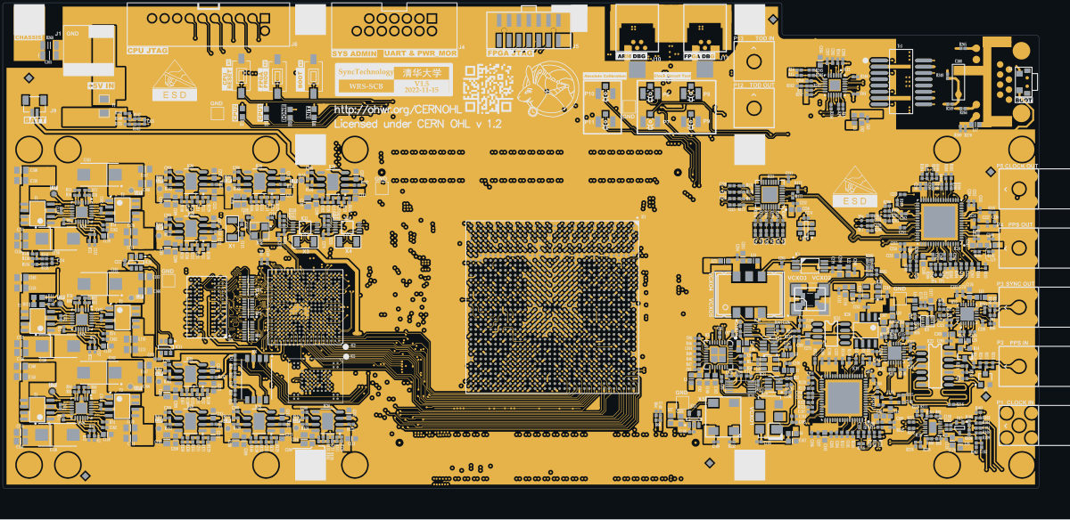
WRS FL SCB (OHWR0044 R1) is an open-hardware circuit board from the CERN Open Hardware Repository, designed in Altium Designer: a 13-layer board of 210 × 98.5 mm with 993 components and 851 nets, published under CERN-OHL-1.2.
review 81% walked · 20 findings: 2 blocker · 12 major · 6 minor (76 items)
Open in the interactive viewerRead the full review
Design review
Probe recorded 20 findings: 2 blocker · 12 major · 6 minor (76 items) on this design. Each is shown here with its reasoning; the full review links every one to the pins, nets and datasheet pages it rests on.
R52 is shorted by duplicate DAC_DMTD_OUT labels, so IC38 drives the 100 nF C103 directly
R52 (470R) is shorted by two DAC_DMTD_OUT net labels, so DAC IC38 drives the 100 nF C103 directly, 10 to 50 times the AD5683R's specified capacitive-load stability limit.
What is wired
On sheet CLK_25M_DMTD (schematic page 20), the net label DAC_DMTD_OUT is placed on both sides of R52:
- DAC side: IC38.10 Vout (and the unfitted IC10.3/4)
- VCXO side: C103, C104, VCXO1.1 VCtrl
The two labels merge both ends into one net. The PCB netlist agrees: R52.1 and R52.2 are both on DAC_DMTD_OUT. The intended 470R + 100 nF RC filter between the DAC and the VCXO control input is therefore bypassed.
``
mermaid flowchart LR DAC["IC38.10 Vout<br/>(AD5683R)"] --- N(("DAC_DMTD_OUT")) N --- R1["R52.1"] R2["R52.2"] --- N N --- C["C103 100 nF to GND"] N --- V["VCXO1.1 VCtrl"]``Limit vs actual
Quantity Limit (AD5683R Rev. D p.4) Actual on board Capacitive load, RL = infinite 2 nF 100 nF (C103, fitted) Capacitive load, RL = 2 kOhm 10 nF 100 nF (C103, fitted) The load is 10 to 50 times the specified range, so the DAC output amplifier may ring or oscillate, and DAC noise reaches VCtrl unfiltered.
Reference
The sister channel on the same board is drawn correctly: IC40 drives DAC_OUT, R53 (470R) feeds DAC_REF_OUT, and C110 (100 nF) sits on the far side.
- NetCopperSplitblockerOpen
CHASSIS's copper is in 3 pieces: J8.9 and 1 other piece(s) are not connected to the rest of the net
CHASSIS's copper is in 3 pieces: J8.9 and 1 other piece(s) are not connected to the rest of the net. Piece 1: C300.2, C305.1, FIX1.0, IC13.1, IC35.1, J10.6, J11.6, L17.2 and 1 more pin(s), on TOP_LAYER, MIDLAYER1, MIDLAYER2, MIDLAYER3, MIDLAYER4, MID-LAYER_7 and BOTTOM_LAYER, 53 drill(s), over (-65.91, 35.31) to (136.37, 60.22). Piece 2: J8.9, on BOTTOM_LAYER, over (133.44, 35.6) to (136.23, 37.13). Piece 3: J8.10, on BOTTOM_LAYER, over (133.44, 51.85) to (136.23, 53.38). The export files every one of these pins under the net, so every connectivity check passes; the copper the fab builds leaves them apart. Usually a pour island that touches only one via of its own net, or a track ending short of its copper: join the piece to the net and export again.
At split:CHASSIS
ARM debug TX (2.5 V) cannot reach the CP2102N RXD input-high threshold (VIO - 0.6 V, about 2.7 V)
The ARM debug TX (DTXD, 2.5 V I/O) drives the CP2102N RXD directly, and the CP2102N's input-high threshold (VIO - 0.6 V) is 2.5 V to 3.0 V: an ARM logic 1 is never guaranteed to register.
What is wired
Net CPU_UART2USB_TX connects:
- ARM IC2 ball R6 = PB13 DTXD, a VDDIOP0 line (SAM9G45 p.26); VDDIOP0 balls K9/K10 are on +2V5.
- CP2102N IC15 pin 25 RXD (Table 5.1 p.28).
- R254 4K7 to GND.
There is no translator in this direction. The opposite direction is level-shifted by the designer: CP2102N TXD, then R255 49R9 / R256 133R, to ARM DRXD.
``
mermaid flowchart LR A["IC2 R6 PB13 DTXD<br/>VDDIOP0 = +2V5"] -->|"CPU_UART2USB_TX<br/>max 2.5 V"| B["IC15 pin 25 RXD<br/>VIH = VDD - 0.6 V"] R["R254 4K7"] --- G["GND"] A --- R``Limit vs actual
The CP2102N QFN28 has no VIO pin, so VIO = VDD (p.15 note 2). VDD (pin 6, VDD33_USB2) is the output of its internal regulator, 3.1 V to 3.6 V (p.12). VIH min = VIO - 0.6 V (Table 3.7 p.13).
CP2102N VDD VIH min ARM high level (max) Margin 3.1 V (regulator min) 2.5 V 2.5 V 0 V 3.3 V (nominal) 2.7 V 2.5 V -0.2 V 3.6 V (regulator max) 3.0 V 2.5 V -0.5 V The link relies on typical rather than specified thresholds. It will often work on the bench, because real CMOS thresholds sit near mid-supply.
ARM_PCK0: the ARM IC2 drives a 2.5 V clock (PA31/PCK0) straight into FPGA IC1 ball N33 in bank 15, which is powered at +1V8 (abs max 2.3 V)
Net ARM_PCK0 connects the AT91SAM9G45 IC2 ball V1 (PA31, whose peripheral-B function is the programmable clock PCK0) directly to Virtex-6 XC6VLX240T IC1 ball N33 (IO_L10P_MRCC_15). IC2 drives that line from VDDIOP0 = +2V5, while FPGA bank 15 has VCCO = +1V8. A 2.5 V high level exceeds the FPGA's absolute-maximum input voltage of VCCO + 0.5 V = 2.3 V.
Connection
End Pin Supply of that pin IC2 AT91SAM9G45 V1 = PA31 (MCI1_CK / PCK0) VDDIOP0 (PIO A table, p.25) = +2V5 on this board (balls K9/K10) IC1 XC6VLX240T N33 = IO_L10P_MRCC_15 Bank 15 VCCO = +1V8 ARM_PCK0 has only these two endpoints: no series resistor, divider or translator.
``
mermaid graph LR ARM["IC2 PA31 / PCK0 (VDDIOP0 = +2V5)"] -->|ARM_PCK0, direct| FPGA["IC1 N33, bank 15 (VCCO = +1V8)"]``Limit vs actual
Quantity Limit Actual Margin FPGA VIN, bank 15 (DS152 abs max: -0.5 to VCCO + 0.5 V) 2.3 V about 2.5 V (ARM VOH at VDDIOP0 = 2.5 V, light load) -0.2 V The ARM EBI signals that share banks 15/16 are correctly at 1.8 V (IC2 VDDIOM1 balls D16/F6/G10/G11 on +1V8). This one PIO line comes from the 2.5 V peripheral domain. If PCK0 is enabled (the net name says it is meant to be), the FPGA input is driven about 0.2 V past its absolute maximum on every cycle, with the bank-15 input clamp conducting. Even as a plain PIO input with its reset pull-up enabled, the line idles at about 2.5 V.
Possible fixes
Move ARM_PCK0 to a ball in a 2.5 V FPGA bank, or add a divider or translator.
The sibling board OHWR0053 R1 WRS LJ SCB has the same defect on the same balls (OBS-136).
CP2102N IC15 regulator pins are decoupled with 100 nF (VDD) and 1 uF (VREGIN) where the datasheet requires 4.7 uF + 0.1 uF on each
On the WRS FL SCB, the USB-UART bridge IC15 (CP2102N) has only 100 nF on its regulator output VDD (C301) and 1 µF on its regulator input VREGIN (C302). The datasheet requires 4.7 µF plus 0.1 µF on each power pin.
Where it is
IC15 (CP2102N-A01-GQFN28) is bus-powered through its internal 5 V-to-3.3 V regulator.
Pin Net Role Capacitance fitted VREGIN pin 7, VBUS pin 8 VBUS_USB2 (from backplane J3.94) regulator input C302 only VDD pin 6 VDD33_USB2 regulator output ("VDD Supply Power Input / 5V Regulator Output", pin table p.28) C301 only The parts as fitted
Ref Value Footprint Library reference Source C301 100 nF CC1005-0402 CC0603_100NF_16V_10%_X7R released BOM (wrs-fl-scb-bom.csv), ODB placement C302 1 µF CC1005-0402 CC0603_1UF_25V_10%_X5R released BOM (wrs-fl-scb-bom.csv), ODB placement Both capacitors are placed on 0402 (1005 metric) footprints in the ODB and the BOM. The "CC0603_..." text is only the library reference name. It gives the 25 V X5R (C302) and 16 V X7R (C301) ratings, not the case size.
What the datasheet asks
The bus-powered connection diagram (Figure 2.1, p.5) states "4.7 µF and 0.1 µF bypass capacitors required for each power pin placed as close to the pins as possible". No 4.7 µF capacitor is on either pin.
Quantity Value Source Required per power pin 4.7 µF + 0.1 µF CP2102N datasheet p.5, Figure 2.1 Fitted on VDD (regulator output) 0.1 µF (C301) BOM Fitted on VREGIN (regulator input) 1 µF (C302) BOM VDD capacitance as a share of the requirement about 2 % (0.1 of 4.8 µF) derived Why it matters
The regulator output in particular runs with about 2 % of the required capacitance. That risks regulator instability or droop on USB load transients, and makes the whole USB-UART bridge's supply rest on a single 100 nF part.
WRS FL SCB: 6.3 V tantalums C163_U_DCDC_1, C164_U_DCDC_1 on +3V6 at 57% of rated
C163_U_DCDC_1 and C164_U_DCDC_1 (220 uF 6.3 V tantalum, 'CP2917_220UF_6.3V_20%_TANT') sit on the +3V6 output of IC16_U_DCDC_1 at 57% of rating. If they are MnO2, this exceeds the 50% manufacturers recommend.
Part Rail Voltage Applied / 6.3 V Source C163_U_DCDC_1, C164_U_DCDC_1 +3V6 3.6 V 57% netlist; DCDC sheet (+ on the rail) MnO2 tantalum limit (capacitor guide, citing KEMET T491 p.14, Vishay 40246/EIA-809, AVX TDS-PTNO-0024 1.2.2): about 50% of rated up to 85 C. A polymer tantalum rated 10 V or less is allowed 90% (KEMET T2076 p.32-33).
The same footprint on the other channels (+2V8, +2V5, +1V5, +1V3, +1V0) is at or below 44%. The electrolyte is not stated; a polymer part would pass. Orientation is correct.
- DiffPairMismatchmajorOpen
'EXTREFIN_10M_N' / 'EXTREFIN_10M_P' (pair inferred from names) is pin-count asymmetric (3 vs 2)
Differential pair 'EXTREFIN_10M_N' / 'EXTREFIN_10M_P', INFERRED FROM THE NET NAMES (nothing in the design declares it a pair), is pin-count asymmetric (3 vs 2) - one side reaches a pin the other does not, so the two halves cannot be routed as a matched pair. NOTE: this check does not verify WHICH contact either net reaches; a correctly-symmetric pair can still be swapped at a connector.
At EXTREFIN_10M_N
- SinglePointNetmajorOpen
'FPGA_JTAG.FPGA_TCK' reaches only IC1.AE8
Net 'FPGA_JTAG.FPGA_TCK' is EFFECTIVELY single-point: it is wired to 2 pins but only one is POPULATED - the other connection(s) are DNP (J5.6). The populated end IC1.AE8 is an IC INPUT, so as built it FLOATS. Confirm the depopulation is intended and the input has a defined level another way. If the datasheet defines this input left open (an internal pull, "read as low when left floating", or a tri-level input whose open state is one of its settings), file it on the pin as if_unused (pull_up, pull_down or may_float) with submit_pin_behavior, citing the page, and this finding clears.
At FPGA_JTAG.FPGA_TCK
- DecapOrdermajorOpen
DecapOrder: 2 pins×2
2 checked by the review by Claude walker W2 (Cern session) — 2 different reasons
At IC1.M19, IC22.1
Each finding, with its own headline
IC1.M19IC1 supply pin M19 on '+1V0': the smallest capacitor C2 sits 3.3 mm away, behind C4 at 1.8 mm
IC1 supply pin M19 on '+1V0': the smallest capacitor C2 sits 3.3 mm away, behind C4 at 1.8 mm. IC1.M19: the smallest value, C2 (470 nF), is 3.3 mm from the pin and C4 (4.7 uF) 1.8 mm: the high-frequency part sits behind more inductance than the bulk part, which needs it least. Swap them, or bring the smallest value to the pin: it serves the fastest current and is the one the loop inductance defeats. Distances are pad centre to pin centre in the board plane. The 5 mm radius, the 10x value step and the 1 mm / 1.5x tie tolerance are Probe's starting values.
IC22.1IC22 supply pin 1 on '+3V3': the smallest capacitor C282 sits 2.9 mm away, behind C219 at 1.9 mm
IC22 supply pin 1 on '+3V3': the smallest capacitor C282 sits 2.9 mm away, behind C219 at 1.9 mm. IC22.1: the smallest value, C282 (100 nF), is 2.9 mm from the pin and C219 (1 uF) 1.9 mm: the high-frequency part sits behind more inductance than the bulk part, which needs it least. Swap them, or bring the smallest value to the pin: it serves the fastest current and is the one the loop inductance defeats. Distances are pad centre to pin centre in the board plane. The 5 mm radius, the 10x value step and the 1 mm / 1.5x tie tolerance are Probe's starting values.
- FloatingInputmajorOpen
FloatingInput: 5 nets×5
e.g. “IC1.AF8 on 'FPGA_JTAG.FPGA_TMS' has no driver and no pull” · 5 different statements
At FPGA_JTAG.FPGA_TCK, FPGA_JTAG.FPGA_TDI, FPGA_JTAG.FPGA_TMS, NetR232_2, NetR239_2
Each finding, with its own headline
FPGA_JTAG.FPGA_TCKIC1.AE8 on 'FPGA_JTAG.FPGA_TCK' has no driver and no pull
Net 'FPGA_JTAG.FPGA_TCK': input(s) IC1.AE8 with no driver and no pull — floating input (undefined level); add a driver or a pull resistor.
FPGA_JTAG.FPGA_TDIIC1.AD8 on 'FPGA_JTAG.FPGA_TDI' has no driver and no pull
Net 'FPGA_JTAG.FPGA_TDI': input(s) IC1.AD8 with no driver and no pull — floating input (undefined level); add a driver or a pull resistor.
FPGA_JTAG.FPGA_TMSIC1.AF8 on 'FPGA_JTAG.FPGA_TMS' has no driver and no pull
Net 'FPGA_JTAG.FPGA_TMS': input(s) IC1.AF8 with no driver and no pull — floating input (undefined level); add a driver or a pull resistor.
NetR232_2X5.1 on 'NetR232_2' has no driver and no pull
Net 'NetR232_2': input(s) X5.1 with no driver and no pull — floating input (undefined level); add a driver or a pull resistor.
NetR239_2X6.1 on 'NetR239_2' has no driver and no pull
Net 'NetR239_2': input(s) X6.1 with no driver and no pull — floating input (undefined level); add a driver or a pull resistor.
- PartLifecyclemajorOpen
PartLifecycle: 11 part numbers×11
8 Obsolete, 1 Not For New Designs, 1 Discontinued at DigiKey, 1 Last Time Buy · on 17 placements
At D13, IC11, IC15, IC18, IC2, IC5 and 5 more
Each finding, with its own headline
D13HSMS-281C-TR1G on D13: the distributor catalogue reports "Obsolete" for Broadcom Limited's HSMS-281C-TR1G
HSMS-281C-TR1G on D13: the distributor catalogue reports "Obsolete" for Broadcom Limited's HSMS-281C-TR1G — a sourcing/longevity risk to confirm against the MANUFACTURER before acting. This board's BOM names no manufacturer for it, so whether that is the fitted maker's product was not checked. A distributor delisting is not the same claim as the part being unavailable; check the vendor's own lifecycle/product-change notice for the status and any named successor. Re-read the source: GET /api/odb/parts/HSMS-281C-TR1G/providers (which provider said it, the maker and part number it matched, its own words, and when we asked). THE LAST BUY DATE HAS PASSED (2018-06-01, 3,089 day(s) ago), so this is a substitution rather than a buy. The distributor reports NONE left. No approved alternate is recorded for this position.
IC11DS90LV011ATMF on IC11: the distributor catalogue reports "Obsolete" for Texas Instruments's DS90LV011ATMF
DS90LV011ATMF on IC11: the distributor catalogue reports "Obsolete" for Texas Instruments's DS90LV011ATMF — a sourcing/longevity risk to confirm against the MANUFACTURER before acting. This board's BOM names no manufacturer for it, so whether that is the fitted maker's product was not checked. A distributor delisting is not the same claim as the part being unavailable; check the vendor's own lifecycle/product-change notice for the status and any named successor. Re-read the source: GET /api/odb/parts/DS90LV011ATMF/providers (which provider said it, the maker and part number it matched, its own words, and when we asked). THE LAST BUY DATE HAS PASSED (2025-04-10, 584 day(s) ago), so this is a substitution rather than a buy. The distributor reports 59,366 left. No approved alternate is recorded for this position.
IC15CP2102N-A01-GQFN28 on IC15: the distributor catalogue reports "Obsolete" for Silicon Labs's CP2102N-A01-GQFN28
CP2102N-A01-GQFN28 on IC15: the distributor catalogue reports "Obsolete" for Silicon Labs's CP2102N-A01-GQFN28 — a sourcing/longevity risk to confirm against the MANUFACTURER before acting. This board's BOM names no manufacturer for it, so whether that is the fitted maker's product was not checked. A distributor delisting is not the same claim as the part being unavailable; check the vendor's own lifecycle/product-change notice for the status and any named successor. Re-read the source: GET /api/odb/parts/CP2102N-A01-GQFN28/providers (which provider said it, the maker and part number it matched, its own words, and when we asked). No approved alternate is recorded for this position.
IC18LTC6957IDD-2#PBF on IC18: the distributor catalogue reports "Obsolete" for Analog Devices Inc.'s LTC6957IDD-2#PBF
LTC6957IDD-2#PBF on IC18: the distributor catalogue reports "Obsolete" for Analog Devices Inc.'s LTC6957IDD-2#PBF — a sourcing/longevity risk to confirm against the MANUFACTURER before acting. This board's BOM names no manufacturer for it, so whether that is the fitted maker's product was not checked. A distributor delisting is not the same claim as the part being unavailable; check the vendor's own lifecycle/product-change notice for the status and any named successor. Re-read the source: GET /api/odb/parts/LTC6957IDD-2#PBF/providers (which provider said it, the maker and part number it matched, its own words, and when we asked). THE LAST BUY DATE HAS PASSED (2025-01-17, 667 day(s) ago), so this is a substitution rather than a buy. The distributor reports NONE left. No approved alternate is recorded for this position.
IC2AT91SAM9G45-CU on IC2: the distributor catalogue reports "Obsolete" for Microchip Technology's AT91SAM9G45-CU
AT91SAM9G45-CU on IC2: the distributor catalogue reports "Obsolete" for Microchip Technology's AT91SAM9G45-CU — a sourcing/longevity risk to confirm against the MANUFACTURER before acting. This board's BOM names no manufacturer for it, so whether that is the fitted maker's product was not checked. A distributor delisting is not the same claim as the part being unavailable; check the vendor's own lifecycle/product-change notice for the status and any named successor. Re-read the source: GET /api/odb/parts/AT91SAM9G45-CU/providers (which provider said it, the maker and part number it matched, its own words, and when we asked). THE LAST BUY DATE HAS PASSED (2013-09-01, 4,823 day(s) ago), so this is a substitution rather than a buy. The distributor reports NONE left. No approved alternate is recorded for this position.
IC5MT29F4G16ABBDAH4-ITD on IC5: the distributor catalogue reports "Obsolete" for Micron Technology Inc.'s MT29F4G16ABBDAH4-IT:D
MT29F4G16ABBDAH4-ITD on IC5: the distributor catalogue reports "Obsolete" for Micron Technology Inc.'s MT29F4G16ABBDAH4-IT:D — a sourcing/longevity risk to confirm against the MANUFACTURER before acting. This board's BOM names no manufacturer for it, so whether that is the fitted maker's product was not checked. A distributor delisting is not the same claim as the part being unavailable; check the vendor's own lifecycle/product-change notice for the status and any named successor. Re-read the source: GET /api/odb/parts/MT29F4G16ABBDAH4-ITD/providers (which provider said it, the maker and part number it matched, its own words, and when we asked). THE LAST BUY DATE HAS PASSED (2026-08-31, 76 day(s) ago), so this is a substitution rather than a buy. The distributor reports NONE left. No approved alternate is recorded for this position.
IC6AT45DB321D-SU on IC6: the distributor catalogue reports "Obsolete" for Renesas Electronics Corporation's AT45DB321D-SU
AT45DB321D-SU on IC6: the distributor catalogue reports "Obsolete" for Renesas Electronics Corporation's AT45DB321D-SU — a sourcing/longevity risk to confirm against the MANUFACTURER before acting. This board's BOM names no manufacturer for it, so whether that is the fitted maker's product was not checked. A distributor delisting is not the same claim as the part being unavailable; check the vendor's own lifecycle/product-change notice for the status and any named successor. Re-read the source: GET /api/odb/parts/AT45DB321D-SU/providers (which provider said it, the maker and part number it matched, its own words, and when we asked). No approved alternate is recorded for this position.
IC7MT47H32M16NF-25EIT:H on IC7: the distributor catalogue reports "Last Time Buy" for Micron Technology Inc.'s MT47H32M16NF-25E IT:H
MT47H32M16NF-25EIT:H on IC7: the distributor catalogue reports "Last Time Buy" for Micron Technology Inc.'s MT47H32M16NF-25E IT:H — a sourcing/longevity risk to confirm against the MANUFACTURER before acting. This board's BOM names no manufacturer for it, so whether that is the fitted maker's product was not checked. A distributor delisting is not the same claim as the part being unavailable; check the vendor's own lifecycle/product-change notice for the status and any named successor. Re-read the source: GET /api/odb/parts/MT47H32M16NF-25EIT:H/providers (which provider said it, the maker and part number it matched, its own words, and when we asked). LAST BUY 2027-03-01 — 106 day(s) remaining to place a final order. The distributor reports 1,757 left. No approved alternate is recorded for this position.
T1_U_DCDC_1IRF9910Pbf on 6 placements (T1_U_DCDC_1, T1_U_DCDC_2, T1_U_DCDC_3, T2_U_DCDC_1, T2_U_DCDC_2, T2_U_DCDC_3): the distributor catalogue reports "Discontinued at DigiKey" for Infineon Technologies's IRF9910PBF
IRF9910Pbf on 6 placements (T1_U_DCDC_1, T1_U_DCDC_2, T1_U_DCDC_3, T2_U_DCDC_1, T2_U_DCDC_2, T2_U_DCDC_3): the distributor catalogue reports "Discontinued at DigiKey" for Infineon Technologies's IRF9910PBF — a sourcing/longevity risk to confirm against the MANUFACTURER before acting. This board's BOM names no manufacturer for it, so whether that is the fitted maker's product was not checked. A distributor delisting is not the same claim as the part being unavailable; check the vendor's own lifecycle/product-change notice for the status and any named successor. Re-read the source: GET /api/odb/parts/IRF9910Pbf/providers (which provider said it, the maker and part number it matched, its own words, and when we asked). No approved alternate is recorded for this position.
X1ABS09-32.768KHZ-T on X1: the distributor catalogue reports "Not For New Designs" for Abracon LLC's ABS09-32.768KHZ-T
ABS09-32.768KHZ-T on X1: the distributor catalogue reports "Not For New Designs" for Abracon LLC's ABS09-32.768KHZ-T — a sourcing/longevity risk to confirm against the MANUFACTURER before acting. This board's BOM names no manufacturer for it, so whether that is the fitted maker's product was not checked. A distributor delisting is not the same claim as the part being unavailable; check the vendor's own lifecycle/product-change notice for the status and any named successor. Re-read the source: GET /api/odb/parts/ABS09-32.768KHZ-T/providers (which provider said it, the maker and part number it matched, its own words, and when we asked). No approved alternate is recorded for this position.
X57W-25.000MBE-T on 2 placements (X5, X6): the distributor catalogue reports "Obsolete" for TXC CORPORATION's 7W-25.000MBE-T
7W-25.000MBE-T on 2 placements (X5, X6): the distributor catalogue reports "Obsolete" for TXC CORPORATION's 7W-25.000MBE-T — a sourcing/longevity risk to confirm against the MANUFACTURER before acting. This board's BOM names no manufacturer for it, so whether that is the fitted maker's product was not checked. A distributor delisting is not the same claim as the part being unavailable; check the vendor's own lifecycle/product-change notice for the status and any named successor. Re-read the source: GET /api/odb/parts/7W-25.000MBE-T/providers (which provider said it, the maker and part number it matched, its own words, and when we asked). THE LAST BUY DATE HAS PASSED (2022-01-29, 1,751 day(s) ago), so this is a substitution rather than a buy. The distributor reports NONE left. No approved alternate is recorded for this position.
- ReferencePlaneDiscontinuitymajorOpen
ReferencePlaneDiscontinuity: 34 boards×34
e.g. “'NetR235_1' runs ALONG the split between the CHASSIS and GND planes on GND3 at 1 place, the longest 2.11 mm; the impedance rises from 20 ohm to 25 ohm there at worst, 12.6 % of each edge reflected (fastest: NetR235_1 at 100 ps 10-90 %, ASSUMED)” · 34 different statements
At along@GND3:CHASSIS|GND, along@PWR3:+1V2_GTX|GND, along@PWR3:+2V5_PLL|+3V3_EXTPLL, gap:PWR3:hole 24.69,10.92|71.81,11.41, refchange:+1V0_GTX|GND, refchange:+1V0|GND and 28 more
Each finding, with its own headline
along@GND3:CHASSIS|GND'NetR235_1' runs ALONG the split between the CHASSIS and GND planes on GND3 at 1 place, the longest 2.11 mm; the impedance rises from 20 ohm to 25 ohm there at worst, 12.6 % of each edge reflected (fastest: NetR235_1 at 100 ps 10-90 %, ASSUMED)
On GND3 the CHASSIS and GND planes part, and 'NetR235_1' runs down the slot between them at 1 place(s), rather than across it. This is not a crossing: the return still follows the track, in the plane on its other side and in the slot's edges, so it does not detour. What changes is the track's own impedance. With the plane gone from under it on this side for that length, its field reaches further, to the slot's edges and to the next plane beyond, so its capacitance falls and its impedance rises; every edge travelling down it is partly reflected where it enters the stretch and again where it leaves, by (Z2 - Z1)/(Z2 + Z1). The longer the stretch against the edge's rise, the more of the edge sees the full step. A crossing is generally the worse fault; a mismatch is not free. Over solid plane each track is 20 ohm; along the slot 25 ohm, reflecting up to 12.6 % of each edge (a method-of-moments field solve of the cross-section, one dielectric; were the slot's edges to carry none of the return, up to 66 ohm). No place stays within 10 %, the tolerance controlled impedance is commonly built to (the stackup states none), so the finding is a warning. One decision covers the split line's slot: whether these tracks may run down it, or should be moved over solid plane.
- 'NetR235_1' on BOTTOM_LAYER at (79.74, 56.79), 2.47 mm, running ALONG the split for 2.11 mm, not across it, 20 ohm over solid plane, 25 ohm along it: 12.6 % of each edge reflected; other side: none: the signal layer is outermost
Every site is a row of this finding's evidence, keyed by net, layers and position. GET /api/odb/boards/45/reference-planes?group=along%40GND3%3ACHASSIS%7CGND serves each with its own layer_image region; all of them lie in x 78.68..80.93, y 54.55..58.91 mm (board frame, Y up).
Read from the copper as drawn on the reference layer, along each track's centreline at exact breakpoints. The reference is the copper beside the track, never the layer's type or name. Whether it matters depends on each signal's edge rate, which nothing on file states for these nets: a slow static line crosses a split harmlessly, a fast edge does not.
along@PWR3:+1V2_GTX|GND2 nets run ALONG the split between the +1V2_GTX and GND planes on PWR3 at 2 places, the longest 10.72 mm; the impedance rises from 65 ohm to 73 ohm there at worst, 5.4 % of each edge reflected (fastest: FPGA_DONE at 100 ps 10-90 %, ASSUMED)
On PWR3 the +1V2_GTX and GND planes part, and 2 nets run down the slot between them at 2 place(s), rather than across it. This is not a crossing: the return still follows the track, in the plane on its other side and in the slot's edges, so it does not detour. What changes is the track's own impedance. With the plane gone from under it on this side for that length, its field reaches further, to the slot's edges and to the next plane beyond, so its capacitance falls and its impedance rises; every edge travelling down it is partly reflected where it enters the stretch and again where it leaves, by (Z2 - Z1)/(Z2 + Z1). The longer the stretch against the edge's rise, the more of the edge sees the full step. A crossing is generally the worse fault; a mismatch is not free. Over solid plane each track is 65 ohm; along the slot 70 ohm to 73 ohm, reflecting up to 5.4 % of each edge (a method-of-moments field solve of the cross-section, one dielectric; were the slot's edges to carry none of the return, up to 87 ohm). At 1 of the 2 place(s) the rise is within 10 %, the tolerance controlled impedance is commonly built to (the stackup states none); the rest exceed it or cannot be said, so the finding is a warning. One decision covers the split line's slot: whether these tracks may run down it, or should be moved over solid plane.
- 'CPU_UART2USB_RX' on MIDLAYER4 at (9.54, 35.59), 3.37 mm, running ALONG the split for 3.02 mm, not across it, 65 ohm over solid plane, 73 ohm along it: 5.4 % of each edge reflected; other side: no plane on MID-LAYER_7
- 'FPGA_DONE' on MIDLAYER4 at (20.55, 35.64), 11.02 mm, running ALONG the split for 10.72 mm, not across it, 65 ohm over solid plane, 70 ohm along it: 3.4 % of each edge reflected; other side: no plane on MID-LAYER_7
Every site is a row of this finding's evidence, keyed by net, layers and position. GET /api/odb/boards/45/reference-planes?group=along%40PWR3%3A%2B1V2_GTX%7CGND serves each with its own layer_image region; all of them lie in x 6.88..26.91, y 34.42..36.69 mm (board frame, Y up).
Read from the copper as drawn on the reference layer, along each track's centreline at exact breakpoints. The reference is the copper beside the track, never the layer's type or name. Whether it matters depends on each signal's edge rate, which nothing on file states for these nets: a slow static line crosses a split harmlessly, a fast edge does not.
along@PWR3:+2V5_PLL|+3V3_EXTPLL2 nets run ALONG the split between the +2V5_PLL and +3V3_EXTPLL planes on PWR3 at 2 places, the longest 14 mm; the impedance rises from 65 ohm to 72 ohm there at worst, 5 % of each edge reflected (fastest: CLK_62_5MHZ_P at 1 ns 10-90 %, suggested by its name)
On PWR3 the +2V5_PLL and +3V3_EXTPLL planes part, and 2 nets run down the slot between them at 2 place(s), rather than across it. This is not a crossing: the return still follows the track, in the plane on its other side and in the slot's edges, so it does not detour. What changes is the track's own impedance. With the plane gone from under it on this side for that length, its field reaches further, to the slot's edges and to the next plane beyond, so its capacitance falls and its impedance rises; every edge travelling down it is partly reflected where it enters the stretch and again where it leaves, by (Z2 - Z1)/(Z2 + Z1). The longer the stretch against the edge's rise, the more of the edge sees the full step. A crossing is generally the worse fault; a mismatch is not free. Over solid plane each track is 65 ohm; along the slot 72 ohm, reflecting up to 5 % of each edge (a method-of-moments field solve of the cross-section, one dielectric; were the slot's edges to carry none of the return, up to 87 ohm). At 1 of the 2 place(s) the rise is within 10 %, the tolerance controlled impedance is commonly built to (the stackup states none); the rest exceed it or cannot be said, so the finding is a warning. One decision covers the split line's slot: whether these tracks may run down it, or should be moved over solid plane.
- 'FPGA_GPIO1' on MIDLAYER4 at (60.24, -30.33), 12.03 mm, running ALONG the split for 11.53 mm, not across it, 65 ohm over solid plane, 72 ohm along it: 5 % of each edge reflected; other side: no plane on MID-LAYER_7
- 'CLK_62_5MHZ_P' on MIDLAYER4 at (41.68, -30.36), 14.36 mm, running ALONG the split for 14 mm, not across it, 66 ohm over solid plane, 72 ohm along it: 4.3 % of each edge reflected; other side: no plane on MID-LAYER_7
Every site is a row of this finding's evidence, keyed by net, layers and position. GET /api/odb/boards/45/reference-planes?group=along%40PWR3%3A%2B2V5_PLL%7C%2B3V3_EXTPLL serves each with its own layer_image region; all of them lie in x 33.48..67.18, y -31.41..-29.16 mm (board frame, Y up).
Read from the copper as drawn on the reference layer, along each track's centreline at exact breakpoints. The reference is the copper beside the track, never the layer's type or name. Whether it matters depends on each signal's edge rate, which nothing on file states for these nets: a slow static line crosses a split harmlessly, a fast edge does not.
gap:PWR3:hole 24.69,10.92|71.81,11.41'TOD_OUT' crosses one gap in PWR3's negative-plane field at 1 place, the longest 0.36 mm (fastest: TOD_OUT at 100 ps 10-90 %, ASSUMED)
Along 'TOD_OUT' on MIDLAYER4, PWR3 is a negative layer (copper everywhere inside the profile), and its field is cleared for 0.36 mm under the track at (61.54, 11.09). The layer does not state the nets either side, so whether this is a split between two planes or a void in one is not said; either way the return current has to go round it. What cleared it: the hole at x 24.69..71.81, y 10.92..11.41. One decision covers the void: whether these tracks may cross it, or the plane should be filled under them. No crossing has a plane on the track's other side, so the whole return meets the break.
- 'TOD_OUT' on MIDLAYER4 at (61.54, 11.09), 0.36 mm; other side: no plane on MID-LAYER_7
Every site is a row of this finding's evidence, keyed by net, layers and position. GET /api/odb/boards/45/reference-planes?group=gap%3APWR3%3Ahole%2024.69%2C10.92%7C71.81%2C11.41 serves each with its own layer_image region; all of them lie in x 60.41..62.67, y 9.97..12.22 mm (board frame, Y up).
Read from the copper as drawn on the reference layer, along each track's centreline at exact breakpoints. The reference is the copper beside the track, never the layer's type or name. Whether it matters depends on each signal's edge rate, which nothing on file states for these nets: a slow static line crosses a split harmlessly, a fast edge does not.
refchange:+1V0_GTX|GND16 nets change reference between +1V0_GTX and GND at 19 vias, none with a reference that continues across (fastest: DONE at 100 ps 10-90 %, ASSUMED)
At 19 via(s), on 16 net(s), the signal leaves a layer referenced by one of +1V0_GTX and GND for a layer referenced by the other, and no plane references both layers. Different nets: no via can carry the return across; only decoupling between the two planes near the via can. The capacitor carrying the return across was measured at each via, at the knee of the crossing net's edge against 50 ohm assumed: 19 with none. 19 of them at an ASSUMED edge (no edge on file for the net): state one (net_timing_state) and it is re-read. One decision covers the pair: whether +1V0_GTX and GND are decoupled to each other near these vias. A via whose layers have more references than these two is a site of each pair it joins. None is partial: at every one, no reference continues across the via.
- 'PLL_CLKS.REF_CLK_P' at (52.2, 7.8), TOP_LAYER -> MIDLAYER4: GND on GND1 to +1V0_GTX on PWR3; pure, no reference continues across; stitching none, 63.0 mm of track past the via on MIDLAYER4: At the 5 GHz knee of a 100 ps edge (1 ns 10-90 %, assumed: no edge is on file for the net) no capacitor carries the return; only the planes do. +1V0_GTX and GND are not a thin pair (at most 0.2 mm), so their own capacitance does not carry the return. To serve it, change layers across the same plane, or move the signal to a layer referenced to ground. None.
- 'PLL_CLKS.REF_CLK_N' at (53.2, 7.8), TOP_LAYER -> MIDLAYER4: GND on GND1 to +1V0_GTX on PWR3; pure, no reference continues across; stitching none, 62.9 mm of track past the via on MIDLAYER4: At the 5 GHz knee of a 100 ps edge (1 ns 10-90 %, assumed: no edge is on file for the net) no capacitor carries the return; only the planes do. +1V0_GTX and GND are not a thin pair (at most 0.2 mm), so their own capacitance does not carry the return. To serve it, change layers across the same plane, or move the signal to a layer referenced to ground. Measured for reference: C22 (4.7 uF 0603) 2.7 mm away: 1.15 nH in the 0.940 mm cavity + 0.51 nH ESL + 1.06 nH mounting (pad 0.10 nH + no via of the second net within 1 mm of its pad: the study's 0.6 nH per mm of 1.60 mm depth, ASSUMED): 85.5 ohm at the knee, 171 % of 50 ohm (assumed track impedance). None.
- 'AUX_CLK_P' at (60.2, 6.8), TOP_LAYER -> MIDLAYER4: GND on GND1 to +1V0_GTX on PWR3; pure, no reference continues across; stitching none, 56.6 mm of track past the via on MIDLAYER4: At the 5 GHz knee of a 100 ps edge (1 ns 10-90 %, assumed: no edge is on file for the net) no capacitor carries the return; only the planes do. +1V0_GTX and GND are not a thin pair (at most 0.2 mm), so their own capacitance does not carry the return. To serve it, change layers across the same plane, or move the signal to a layer referenced to ground. None.
- 'AUX_CLK_N' at (59.2, 6.8), TOP_LAYER -> MIDLAYER4: GND on GND1 to +1V0_GTX on PWR3; pure, no reference continues across; stitching none, 56.6 mm of track past the via on MIDLAYER4: At the 5 GHz knee of a 100 ps edge (1 ns 10-90 %, assumed: no edge is on file for the net) no capacitor carries the return; only the planes do. +1V0_GTX and GND are not a thin pair (at most 0.2 mm), so their own capacitance does not carry the return. To serve it, change layers across the same plane, or move the signal to a layer referenced to ground. None.
- 'PROGRAM_B' at (50.2, 8.8), TOP_LAYER -> MIDLAYER3: GND on GND1 to +2V5 on PWR2, +1V0_GTX on PWR3; pure, no reference continues across; stitching none, 43.1 mm of track past the via on MIDLAYER3: At the 5 GHz knee of a 100 ps edge (100 ps 10-90 %, assumed: no edge is on file for the net) no capacitor carries the return; only the planes do. +1V0_GTX and GND are not a thin pair (at most 0.2 mm), so their own capacitance does not carry the return. To serve it, change layers across the same plane, or move the signal to a layer referenced to ground. Measured for reference: C60 (220 nF 0402) 2.1 mm away: 1.05 nH in the 0.940 mm cavity + 0.30 nH ESL + 1.03 nH mounting (pad 0.07 nH + no via of the first net within 1 mm of its pad: the study's 0.6 nH per mm of 1.60 mm depth, ASSUMED): 74.9 ohm at the knee, 150 % of 50 ohm (assumed track impedance). None.
- 'TOD_TERM_EN' at (60.66, 9.25), TOP_LAYER -> MIDLAYER4: GND on GND1 to +1V0_GTX on PWR3; pure, no reference continues across; stitching none, 42.8 mm of track past the via on MIDLAYER4: At the 5 GHz knee of a 100 ps edge (20 ns 10-90 %, assumed: no edge is on file for the net) no capacitor carries the return; only the planes do. +1V0_GTX and GND are not a thin pair (at most 0.2 mm), so their own capacitance does not carry the return. To serve it, change layers across the same plane, or move the signal to a layer referenced to ground. Measured for reference: C40 (220 nF 0402) 2.5 mm away: 1.12 nH in the 0.940 mm cavity + 0.30 nH ESL + 1.03 nH mounting (pad 0.07 nH + no via of the second net within 1 mm of its pad: the study's 0.6 nH per mm of 1.60 mm depth, ASSUMED): 77.2 ohm at the knee, 154 % of 50 ohm (assumed track impedance). None.
- 'INIT_B' at (47.2, 8.8), TOP_LAYER -> MIDLAYER3: GND on GND1 to +2V5 on PWR2, +1V0_GTX on PWR3; pure, no reference continues across; stitching none, 42.4 mm of track past the via on MIDLAYER3: At the 5 GHz knee of a 100 ps edge (100 ps 10-90 %, assumed: no edge is on file for the net) no capacitor carries the return; only the planes do. +1V0_GTX and GND are not a thin pair (at most 0.2 mm), so their own capacitance does not carry the return. To serve it, change layers across the same plane, or move the signal to a layer referenced to ground. Measured for reference: C60 (220 nF 0402) 1.1 mm away: 0.81 nH in the 0.940 mm cavity + 0.30 nH ESL + 1.03 nH mounting (pad 0.07 nH + no via of the first net within 1 mm of its pad: the study's 0.6 nH per mm of 1.60 mm depth, ASSUMED): 67.4 ohm at the knee, 135 % of 50 ohm (assumed track impedance). None.
- 'DONE' at (46.2, 8.8), TOP_LAYER -> MIDLAYER3: GND on GND1 to +2V5 on PWR2, +1V0_GTX on PWR3; pure, no reference continues across; stitching none, 36.2 mm of track past the via on MIDLAYER3: At the 5 GHz knee of a 100 ps edge (100 ps 10-90 %, assumed: no edge is on file for the net) no capacitor carries the return; only the planes do. +1V0_GTX and GND are not a thin pair (at most 0.2 mm), so their own capacitance does not carry the return. To serve it, change layers across the same plane, or move the signal to a layer referenced to ground. Measured for reference: C60 (220 nF 0402) 2.0 mm away: 1.04 nH in the 0.940 mm cavity + 0.30 nH ESL + 1.03 nH mounting (pad 0.07 nH + no via of the first net within 1 mm of its pad: the study's 0.6 nH per mm of 1.60 mm depth, ASSUMED): 74.7 ohm at the knee, 149 % of 50 ohm (assumed track impedance). None.
- '+3V3_PG' at (15.1, 9.8), MIDLAYER2 -> MIDLAYER3: +1V0 on PWR1, GND on GND2 to +2V5 on PWR2, +1V0_GTX on PWR3; pure, no reference continues across; stitching none, 22.9 mm of track past the via on MIDLAYER3: At the 5 GHz knee of a 100 ps edge (20 ns 10-90 %, assumed: no edge is on file for the net) no capacitor carries the return; only the planes do. +1V0_GTX and GND are not a thin pair (at most 0.2 mm), so their own capacitance does not carry the return. To serve it, change layers across the same plane, or move the signal to a layer referenced to ground. None.
- '+1V2_GTX_PG' at (14.5, 10.3), MIDLAYER2 -> MIDLAYER3: +1V0 on PWR1, GND on GND2 to +2V5 on PWR2, +1V0_GTX on PWR3; pure, no reference continues across; stitching none, 22.3 mm of track past the via on MIDLAYER3: At the 5 GHz knee of a 100 ps edge (20 ns 10-90 %, assumed: no edge is on file for the net) no capacitor carries the return; only the planes do. +1V0_GTX and GND are not a thin pair (at most 0.2 mm), so their own capacitance does not carry the return. To serve it, change layers across the same plane, or move the signal to a layer referenced to ground. None.
- 'ARM_WD_RST' at (-7.25, 14.17), TOP_LAYER -> MIDLAYER4: GND on GND1 to +1V0_GTX on PWR3; pure, no reference continues across; stitching none, 18.1 mm of track past the via on MIDLAYER4: At the 5 GHz knee of a 100 ps edge (20 ns 10-90 %, assumed: no edge is on file for the net) no capacitor carries the return; only the planes do. +1V0_GTX and GND are not a thin pair (at most 0.2 mm), so their own capacitance does not carry the return. To serve it, change layers across the same plane, or move the signal to a layer referenced to ground. None.
- 'ARM_WD_SDA' at (-7.23, 15.67), TOP_LAYER -> MIDLAYER4: GND on GND1 to +1V0_GTX on PWR3; pure, no reference continues across; stitching none, 15.5 mm of track past the via on MIDLAYER4: At the 5 GHz knee of a 100 ps edge (10 ns 10-90 %, assumed: no edge is on file for the net) no capacitor carries the return; only the planes do. +1V0_GTX and GND are not a thin pair (at most 0.2 mm), so their own capacitance does not carry the return. To serve it, change layers across the same plane, or move the signal to a layer referenced to ground. None.
- and 7 more
Every site is a row of this finding's evidence, keyed by net, layers and position. GET /api/odb/boards/45/reference-planes?group=refchange%3A%2B1V0_GTX%7CGND serves each with its own layer_image region; all of them lie in x -15.66..62.66, y 4.8..18.44 mm (board frame, Y up).
The reference on each layer is the first plane the track meets leaving the via, anti-pads and the net's own copper skipped. Whether it matters depends on each signal's edge rate, which nothing on file states for these nets: a slow static line crosses a split harmlessly, a fast edge does not.
refchange:+1V0|GND126 nets change reference between +1V0 and GND at 171 vias; 135 of them partial (fastest: CPU_LED1 at 100 ps 10-90 %, ASSUMED)
At 171 via(s), on 126 net(s), the signal leaves a layer referenced by one of +1V0 and GND for a layer referenced by the other, and no plane references both layers. Different nets: no via can carry the return across; only decoupling between the two planes near the via can. The capacitor carrying the return across was measured at each via, at the knee of the crossing net's edge against 50 ohm assumed: 171 with none. 171 of them at an ASSUMED edge (no edge on file for the net): state one (net_timing_state) and it is re-read. One decision covers the pair: whether +1V0 and GND are decoupled to each other near these vias. A via whose layers have more references than these two is a site of each pair it joins. 135 of them are partial: another reference continues across through a stitching via of its net, so only part of the return has nowhere to go. The pure ones are listed first, then the partial ones with the farthest stitching via first.
- 'nRST' at (1.91, 4.06), TOP_LAYER -> MIDLAYER3: GND on GND1 to +2V5 on PWR2, +1V0 on PWR3; pure, no reference continues across; stitching none, 133.8 mm of track past the via on MIDLAYER3: At the 5 GHz knee of a 100 ps edge (20 ns 10-90 %, assumed: no edge is on file for the net) no capacitor carries the return; only the planes do. +1V0 and GND are not a thin pair (at most 0.2 mm), so their own capacitance does not carry the return. To serve it, change layers across the same plane, or move the signal to a layer referenced to ground. None.
- 'CPU_SSC.TK1' at (-6, 5.2), TOP_LAYER -> MIDLAYER3: GND on GND1 to +2V5 on PWR2, +1V0 on PWR3; pure, no reference continues across; stitching none, 108.8 mm of track past the via on MIDLAYER3: At the 5 GHz knee of a 100 ps edge (100 ps 10-90 %, assumed: no edge is on file for the net) no capacitor carries the return; only the planes do. +1V0 and GND are not a thin pair (at most 0.2 mm), so their own capacitance does not carry the return. To serve it, change layers across the same plane, or move the signal to a layer referenced to ground. None.
- 'CPU_SSC.TD1' at (-5.2, 5.2), TOP_LAYER -> MIDLAYER3: GND on GND1 to +2V5 on PWR2, +1V0 on PWR3; pure, no reference continues across; stitching none, 101.1 mm of track past the via on MIDLAYER3: At the 5 GHz knee of a 100 ps edge (100 ps 10-90 %, assumed: no edge is on file for the net) no capacitor carries the return; only the planes do. +1V0 and GND are not a thin pair (at most 0.2 mm), so their own capacitance does not carry the return. To serve it, change layers across the same plane, or move the signal to a layer referenced to ground. None.
- 'CPU_SSC.RD1' at (-5.21, 4.4), TOP_LAYER -> MIDLAYER3: GND on GND1 to +2V5 on PWR2, +1V0 on PWR3; pure, no reference continues across; stitching none, 98.2 mm of track past the via on MIDLAYER3: At the 5 GHz knee of a 100 ps edge (100 ps 10-90 %, assumed: no edge is on file for the net) no capacitor carries the return; only the planes do. +1V0 and GND are not a thin pair (at most 0.2 mm), so their own capacitance does not carry the return. To serve it, change layers across the same plane, or move the signal to a layer referenced to ground. None.
- 'SDA_TMP' at (6.34, 5.99), MIDLAYER2 -> MIDLAYER3: +1V8 on PWR1, GND on GND2 to +2V5 on PWR2, +1V0 on PWR3; pure, no reference continues across; stitching none, 84.9 mm of track past the via on MIDLAYER3: At the 5 GHz knee of a 100 ps edge (10 ns 10-90 %, assumed: no edge is on file for the net) no capacitor carries the return; only the planes do. +1V0 and GND are not a thin pair (at most 0.2 mm), so their own capacitance does not carry the return. To serve it, change layers across the same plane, or move the signal to a layer referenced to ground. None.
- 'FPGA_JTAG.FPGA_TMS' at (34.2, 8.8), TOP_LAYER -> MIDLAYER2: GND on GND1 to +1V0 on PWR1, GND on GND2; partial, GND continues through a via of GND 1 mm away; stitching none, 84.5 mm of track past the via on MIDLAYER2: At the 5 GHz knee of a 100 ps edge (2 ns 10-90 %, assumed: no edge is on file for the net) no capacitor carries the return; only the planes do. +1V0 and GND are not a thin pair (at most 0.2 mm), so their own capacitance does not carry the return. To serve it, change layers across the same plane, or move the signal to a layer referenced to ground. None.
- 'SCL_TMP' at (6.2, 6.67), MIDLAYER2 -> MIDLAYER3: +1V8 on PWR1, GND on GND2 to +2V5 on PWR2, +1V0 on PWR3; pure, no reference continues across; stitching none, 82.6 mm of track past the via on MIDLAYER3: At the 5 GHz knee of a 100 ps edge (10 ns 10-90 %, assumed: no edge is on file for the net) no capacitor carries the return; only the planes do. +1V0 and GND are not a thin pair (at most 0.2 mm), so their own capacitance does not carry the return. To serve it, change layers across the same plane, or move the signal to a layer referenced to ground. None.
- 'PB4' at (-9.2, 2), TOP_LAYER -> MIDLAYER3: GND on GND1 to +2V5 on PWR2, +1V0 on PWR3; pure, no reference continues across; stitching none, 82.2 mm of track past the via on MIDLAYER3: At the 5 GHz knee of a 100 ps edge (100 ps 10-90 %, assumed: no edge is on file for the net) no capacitor carries the return; only the planes do. +1V0 and GND are not a thin pair (at most 0.2 mm), so their own capacitance does not carry the return. To serve it, change layers across the same plane, or move the signal to a layer referenced to ground. None.
- 'FPGA_JTAG.FPGA_TCK' at (35.2, 8.8), TOP_LAYER -> MIDLAYER2: GND on GND1 to +1V0 on PWR1, GND on GND2; partial, GND continues through a via of GND 1.41 mm away; stitching none, 81.6 mm of track past the via on MIDLAYER2: At the 5 GHz knee of a 100 ps edge (2 ns 10-90 %, assumed: no edge is on file for the net) no capacitor carries the return; only the planes do. +1V0 and GND are not a thin pair (at most 0.2 mm), so their own capacitance does not carry the return. To serve it, change layers across the same plane, or move the signal to a layer referenced to ground. None.
- 'PB0' at (-9.2, 2.81), TOP_LAYER -> MIDLAYER4: GND on GND1 to +1V0 on PWR3; pure, no reference continues across; stitching none, 78.7 mm of track past the via on MIDLAYER4: At the 5 GHz knee of a 100 ps edge (100 ps 10-90 %, assumed: no edge is on file for the net) no capacitor carries the return; only the planes do. +1V0 and GND are not a thin pair (at most 0.2 mm), so their own capacitance does not carry the return. To serve it, change layers across the same plane, or move the signal to a layer referenced to ground. None.
- 'FPGA_JTAG.FPGA_TDO' at (37.2, 8.8), TOP_LAYER -> MIDLAYER2: GND on GND1 to +1V0 on PWR1, GND on GND2; partial, GND continues through a via of GND 1 mm away; stitching none, 78.5 mm of track past the via on MIDLAYER2: At the 5 GHz knee of a 100 ps edge (2 ns 10-90 %, assumed: no edge is on file for the net) no capacitor carries the return; only the planes do. +1V0 and GND are not a thin pair (at most 0.2 mm), so their own capacitance does not carry the return. To serve it, change layers across the same plane, or move the signal to a layer referenced to ground. Measured for reference: C3 (4.7 uF 0603) 2.0 mm away: 0.31 nH in the 0.280 mm cavity + 0.51 nH ESL + 1.06 nH mounting (pad 0.10 nH + no via of the first net within 1 mm of its pad: the study's 0.6 nH per mm of 1.60 mm depth, ASSUMED): 59.0 ohm at the knee, 118 % of 50 ohm (assumed track impedance). None.
- 'PB5' at (-9.23, 1.19), TOP_LAYER -> MIDLAYER3: GND on GND1 to +2V5 on PWR2, +1V0 on PWR3; pure, no reference continues across; stitching none, 78.0 mm of track past the via on MIDLAYER3: At the 5 GHz knee of a 100 ps edge (100 ps 10-90 %, assumed: no edge is on file for the net) no capacitor carries the return; only the planes do. +1V0 and GND are not a thin pair (at most 0.2 mm), so their own capacitance does not carry the return. To serve it, change layers across the same plane, or move the signal to a layer referenced to ground. None.
- and 159 more
Every site is a row of this finding's evidence, keyed by net, layers and position. GET /api/odb/boards/45/reference-planes?group=refchange%3A%2B1V0%7CGND serves each with its own layer_image region; all of them lie in x -18.9..73.4, y -8..35.63 mm (board frame, Y up).
The reference on each layer is the first plane the track meets leaving the via, anti-pads and the net's own copper skipped. Whether it matters depends on each signal's edge rate, which nothing on file states for these nets: a slow static line crosses a split harmlessly, a fast edge does not.
refchange:+1V2_GTX|GND17 nets change reference between +1V2_GTX and GND at 22 vias, none with a reference that continues across (fastest: CPU_LED1 at 100 ps 10-90 %, ASSUMED)
At 22 via(s), on 17 net(s), the signal leaves a layer referenced by one of +1V2_GTX and GND for a layer referenced by the other, and no plane references both layers. Different nets: no via can carry the return across; only decoupling between the two planes near the via can. The capacitor carrying the return across was measured at each via, at the knee of the crossing net's edge against 50 ohm assumed: 22 with none. 22 of them at an ASSUMED edge (no edge on file for the net): state one (net_timing_state) and it is re-read. One decision covers the pair: whether +1V2_GTX and GND are decoupled to each other near these vias. A via whose layers have more references than these two is a site of each pair it joins. None is partial: at every one, no reference continues across the via.
- 'RX_ER' at (71.25, 32), MIDLAYER1 -> MIDLAYER3: GND on GND1, +1V0 on PWR1 to +2V5 on PWR2, +1V2_GTX on PWR3; pure, no reference continues across; stitching none, 107.9 mm of track past the via on MIDLAYER3: At the 5 GHz knee of a 100 ps edge (3 ns 10-90 %, assumed: no edge is on file for the net) no capacitor carries the return; only the planes do. +1V2_GTX and GND are not a thin pair (at most 0.2 mm), so their own capacitance does not carry the return. To serve it, change layers across the same plane, or move the signal to a layer referenced to ground. None.
- 'RXD0' at (68.83, 31.98), MIDLAYER1 -> MIDLAYER3: GND on GND1, +1V0 on PWR1 to +2V5 on PWR2, +1V2_GTX on PWR3; pure, no reference continues across; stitching none, 100.0 mm of track past the via on MIDLAYER3: At the 5 GHz knee of a 100 ps edge (3 ns 10-90 %, assumed: no edge is on file for the net) no capacitor carries the return; only the planes do. +1V2_GTX and GND are not a thin pair (at most 0.2 mm), so their own capacitance does not carry the return. To serve it, change layers across the same plane, or move the signal to a layer referenced to ground. None.
- 'RXD1' at (68.05, 31.98), MIDLAYER1 -> MIDLAYER3: GND on GND1, +1V0 on PWR1 to +2V5 on PWR2, +1V2_GTX on PWR3; pure, no reference continues across; stitching none, 96.3 mm of track past the via on MIDLAYER3: At the 5 GHz knee of a 100 ps edge (3 ns 10-90 %, assumed: no edge is on file for the net) no capacitor carries the return; only the planes do. +1V2_GTX and GND are not a thin pair (at most 0.2 mm), so their own capacitance does not carry the return. To serve it, change layers across the same plane, or move the signal to a layer referenced to ground. None.
- 'MDC' at (67.36, 31.98), MIDLAYER1 -> MIDLAYER3: GND on GND1, +1V0 on PWR1 to +2V5 on PWR2, +1V2_GTX on PWR3; pure, no reference continues across; stitching none, 94.2 mm of track past the via on MIDLAYER3: At the 5 GHz knee of a 100 ps edge (100 ps 10-90 %, assumed: no edge is on file for the net) no capacitor carries the return; only the planes do. +1V2_GTX and GND are not a thin pair (at most 0.2 mm), so their own capacitance does not carry the return. To serve it, change layers across the same plane, or move the signal to a layer referenced to ground. None.
- 'MDIO' at (66.73, 32), MIDLAYER1 -> MIDLAYER3: GND on GND1, +1V0 on PWR1 to +2V5 on PWR2, +1V2_GTX on PWR3; pure, no reference continues across; stitching none, 94.0 mm of track past the via on MIDLAYER3: At the 5 GHz knee of a 100 ps edge (1 ns 10-90 %, assumed: no edge is on file for the net) no capacitor carries the return; only the planes do. +1V2_GTX and GND are not a thin pair (at most 0.2 mm), so their own capacitance does not carry the return. To serve it, change layers across the same plane, or move the signal to a layer referenced to ground. None.
- 'FPGA_DONE' at (8.64, 28.32), MIDLAYER1 -> MIDLAYER4: GND on GND1, +1V0 on PWR1 to +1V2_GTX on PWR3; pure, no reference continues across; stitching none, 63.9 mm of track past the via on MIDLAYER4: At the 5 GHz knee of a 100 ps edge (100 ps 10-90 %, assumed: no edge is on file for the net) no capacitor carries the return; only the planes do. +1V2_GTX and GND are not a thin pair (at most 0.2 mm), so their own capacitance does not carry the return. To serve it, change layers across the same plane, or move the signal to a layer referenced to ground. None.
- 'FPGA_INIT_B' at (8.51, 29.21), MIDLAYER1 -> MIDLAYER4: GND on GND1, +1V0 on PWR1 to +1V2_GTX on PWR3; pure, no reference continues across; stitching none, 61.3 mm of track past the via on MIDLAYER4: At the 5 GHz knee of a 100 ps edge (100 ps 10-90 %, assumed: no edge is on file for the net) no capacitor carries the return; only the planes do. +1V2_GTX and GND are not a thin pair (at most 0.2 mm), so their own capacitance does not carry the return. To serve it, change layers across the same plane, or move the signal to a layer referenced to ground. None.
- 'SYST_MON_N3' at (3.2, 17.78), MIDLAYER2 -> MIDLAYER4: +1V8 on PWR1, GND on GND2 to +1V2_GTX on PWR3; pure, no reference continues across; stitching none, 36.2 mm of track past the via on MIDLAYER4: At the 5 GHz knee of a 100 ps edge (100 ps 10-90 %, assumed: no edge is on file for the net) no capacitor carries the return; only the planes do. +1V2_GTX and GND are not a thin pair (at most 0.2 mm), so their own capacitance does not carry the return. To serve it, change layers across the same plane, or move the signal to a layer referenced to ground. None.
- 'SYST_MON_P3' at (2.46, 17.78), MIDLAYER2 -> MIDLAYER4: +1V8 on PWR1, GND on GND2 to +1V2_GTX on PWR3; pure, no reference continues across; stitching none, 35.7 mm of track past the via on MIDLAYER4: At the 5 GHz knee of a 100 ps edge (100 ps 10-90 %, assumed: no edge is on file for the net) no capacitor carries the return; only the planes do. +1V2_GTX and GND are not a thin pair (at most 0.2 mm), so their own capacitance does not carry the return. To serve it, change layers across the same plane, or move the signal to a layer referenced to ground. None.
- 'CPU_LED1' at (8.5, 30), MIDLAYER1 -> MIDLAYER3: GND on GND1, +1V0 on PWR1 to +2V5 on PWR2, +1V2_GTX on PWR3; pure, no reference continues across; stitching none, 29.4 mm of track past the via on MIDLAYER3: At the 5 GHz knee of a 100 ps edge (100 ps 10-90 %, assumed: no edge is on file for the net) no capacitor carries the return; only the planes do. +1V2_GTX and GND are not a thin pair (at most 0.2 mm), so their own capacitance does not carry the return. To serve it, change layers across the same plane, or move the signal to a layer referenced to ground. None.
- 'FPGA_INIT_B' at (8.76, 19.69), MIDLAYER1 -> MIDLAYER3: GND on GND1, +1V8 on PWR1 to +2V5 on PWR2, +1V2_GTX on PWR3; pure, no reference continues across; stitching none, 22.4 mm of track past the via on MIDLAYER3: At the 5 GHz knee of a 100 ps edge (100 ps 10-90 %, assumed: no edge is on file for the net) no capacitor carries the return; only the planes do. +1V2_GTX and GND are not a thin pair (at most 0.2 mm), so their own capacitance does not carry the return. To serve it, change layers across the same plane, or move the signal to a layer referenced to ground. None.
- 'FPGA_DONE' at (61.19, 30.24), MIDLAYER4 -> BOTTOM_LAYER: +1V2_GTX on PWR3 to GND on GND3; pure, no reference continues across; stitching none, 13.1 mm of track past the via on BOTTOM_LAYER: At the 5 GHz knee of a 100 ps edge (100 ps 10-90 %, assumed: no edge is on file for the net) no capacitor carries the return; only the planes do. +1V2_GTX and GND are not a thin pair (at most 0.2 mm), so their own capacitance does not carry the return. To serve it, change layers across the same plane, or move the signal to a layer referenced to ground. None.
- and 10 more
Every site is a row of this finding's evidence, keyed by net, layers and position. GET /api/odb/boards/45/reference-planes?group=refchange%3A%2B1V2_GTX%7CGND serves each with its own layer_image region; all of them lie in x 0.46..73.76, y 13.71..34 mm (board frame, Y up).
The reference on each layer is the first plane the track meets leaving the via, anti-pads and the net's own copper skipped. Whether it matters depends on each signal's edge rate, which nothing on file states for these nets: a slow static line crosses a split harmlessly, a fast edge does not.
refchange:+2V5_FANOUT|GND7 nets change reference between +2V5_FANOUT and GND at 7 vias, none with a reference that continues across (fastest: DAC_DMTD.DAC_DIN at 100 ps 10-90 %, ASSUMED)
At 7 via(s), on 7 net(s), the signal leaves a layer referenced by one of +2V5_FANOUT and GND for a layer referenced by the other, and no plane references both layers. Different nets: no via can carry the return across; only decoupling between the two planes near the via can. The capacitor carrying the return across was measured at each via, at the knee of the crossing net's edge against 50 ohm assumed: 7 with none. 7 of them at an ASSUMED edge (no edge on file for the net): state one (net_timing_state) and it is re-read. One decision covers the pair: whether +2V5_FANOUT and GND are decoupled to each other near these vias. A via whose layers have more references than these two is a site of each pair it joins. None is partial: at every one, no reference continues across the via.
- 'EBI1_D14' at (6.68, -19.59), MIDLAYER1 -> MIDLAYER3: GND on GND1, +3V3_PLL on PWR1 to +2V5 on PWR2, +2V5_FANOUT on PWR3; pure, no reference continues across; stitching none, 49.1 mm of track past the via on MIDLAYER3: At the 5 GHz knee of a 100 ps edge (100 ps 10-90 %, assumed: no edge is on file for the net) no capacitor carries the return; only the planes do. +2V5_FANOUT and GND are not a thin pair (at most 0.2 mm), so their own capacitance does not carry the return. To serve it, change layers across the same plane, or move the signal to a layer referenced to ground. None.
- 'DAC_DMTD.DAC_DIN' at (82.07, -16.84), TOP_LAYER -> MIDLAYER3: GND on GND1 to +3V3 on PWR2, +2V5_FANOUT on PWR3; pure, no reference continues across; stitching none, 48.5 mm of track past the via on MIDLAYER3: At the 5 GHz knee of a 100 ps edge (100 ps 10-90 %, assumed: no edge is on file for the net) no capacitor carries the return; only the planes do. +2V5_FANOUT and GND are not a thin pair (at most 0.2 mm), so their own capacitance does not carry the return. To serve it, change layers across the same plane, or move the signal to a layer referenced to ground. None.
- 'EBI1_D8' at (11, -19.84), MIDLAYER2 -> MIDLAYER3: +3V3_PLL on PWR1, GND on GND2 to +2V5 on PWR2, +2V5_FANOUT on PWR3; pure, no reference continues across; stitching none, 45.4 mm of track past the via on MIDLAYER3: At the 5 GHz knee of a 100 ps edge (100 ps 10-90 %, assumed: no edge is on file for the net) no capacitor carries the return; only the planes do. +2V5_FANOUT and GND are not a thin pair (at most 0.2 mm), so their own capacitance does not carry the return. To serve it, change layers across the same plane, or move the signal to a layer referenced to ground. None.
- 'PE13' at (8.3, -23.15), MIDLAYER1 -> MIDLAYER3: GND on GND1, +3V3_PLL on PWR1 to +2V5 on PWR2, +2V5_FANOUT on PWR3; pure, no reference continues across; stitching none, 28.0 mm of track past the via on MIDLAYER3: At the 5 GHz knee of a 100 ps edge (100 ps 10-90 %, assumed: no edge is on file for the net) no capacitor carries the return; only the planes do. +2V5_FANOUT and GND are not a thin pair (at most 0.2 mm), so their own capacitance does not carry the return. To serve it, change layers across the same plane, or move the signal to a layer referenced to ground. None.
- 'PE9' at (7.55, -23.05), MIDLAYER1 -> MIDLAYER3: GND on GND1, +3V3_PLL on PWR1 to +2V5 on PWR2, +2V5_FANOUT on PWR3; pure, no reference continues across; stitching none, 27.1 mm of track past the via on MIDLAYER3: At the 5 GHz knee of a 100 ps edge (100 ps 10-90 %, assumed: no edge is on file for the net) no capacitor carries the return; only the planes do. +2V5_FANOUT and GND are not a thin pair (at most 0.2 mm), so their own capacitance does not carry the return. To serve it, change layers across the same plane, or move the signal to a layer referenced to ground. None.
- 'CLK1_N' at (94.49, 22.9), TOP_LAYER -> MIDLAYER4: GND on GND1 to +2V5_FANOUT on PWR3; pure, no reference continues across; stitching none, 24.7 mm of track past the via on MIDLAYER4: At the 5 GHz knee of a 100 ps edge (1 ns 10-90 %, assumed: no edge is on file for the net) no capacitor carries the return; only the planes do. +2V5_FANOUT and GND are not a thin pair (at most 0.2 mm), so their own capacitance does not carry the return. To serve it, change layers across the same plane, or move the signal to a layer referenced to ground. None.
- 'CLK1_P' at (94.49, 22.4), TOP_LAYER -> MIDLAYER4: GND on GND1 to +2V5_FANOUT on PWR3; pure, no reference continues across; stitching none, 24.2 mm of track past the via on MIDLAYER4: At the 5 GHz knee of a 100 ps edge (1 ns 10-90 %, assumed: no edge is on file for the net) no capacitor carries the return; only the planes do. +2V5_FANOUT and GND are not a thin pair (at most 0.2 mm), so their own capacitance does not carry the return. To serve it, change layers across the same plane, or move the signal to a layer referenced to ground. None.
Every site is a row of this finding's evidence, keyed by net, layers and position. GET /api/odb/boards/45/reference-planes?group=refchange%3A%2B2V5_FANOUT%7CGND serves each with its own layer_image region; all of them lie in x 4.68..96.49, y -25.15..24.9 mm (board frame, Y up).
The reference on each layer is the first plane the track meets leaving the via, anti-pads and the net's own copper skipped. Whether it matters depends on each signal's edge rate, which nothing on file states for these nets: a slow static line crosses a split harmlessly, a fast edge does not.
refchange:+2V5_PLL|GND26 nets change reference between +2V5_PLL and GND at 26 vias, none with a reference that continues across (fastest: CPU_SSC.TF1 at 100 ps 10-90 %, ASSUMED)
At 26 via(s), on 26 net(s), the signal leaves a layer referenced by one of +2V5_PLL and GND for a layer referenced by the other, and no plane references both layers. Different nets: no via can carry the return across; only decoupling between the two planes near the via can. The capacitor carrying the return across was measured at each via, at the knee of the crossing net's edge against 50 ohm assumed: 26 with none. 26 of them at an ASSUMED edge (no edge on file for the net): state one (net_timing_state) and it is re-read. One decision covers the pair: whether +2V5_PLL and GND are decoupled to each other near these vias. A via whose layers have more references than these two is a site of each pair it joins. None is partial: at every one, no reference continues across the via.
- 'miniBACKPLANE_CLK_N' at (115.97, 5.07), TOP_LAYER -> MIDLAYER3: GND on GND1 to +3V3 on PWR2, +2V5_PLL on PWR3; pure, no reference continues across; stitching none, 68.9 mm of track past the via on MIDLAYER3: At the 5 GHz knee of a 100 ps edge (1 ns 10-90 %, assumed: no edge is on file for the net) no capacitor carries the return; only the planes do. +2V5_PLL and GND are not a thin pair (at most 0.2 mm), so their own capacitance does not carry the return. To serve it, change layers across the same plane, or move the signal to a layer referenced to ground. None.
- 'miniBACKPLANE_CLK_P' at (116.73, 5.07), TOP_LAYER -> MIDLAYER3: GND on GND1 to +3V3 on PWR2, +2V5_PLL on PWR3; pure, no reference continues across; stitching none, 68.8 mm of track past the via on MIDLAYER3: At the 5 GHz knee of a 100 ps edge (1 ns 10-90 %, assumed: no edge is on file for the net) no capacitor carries the return; only the planes do. +2V5_PLL and GND are not a thin pair (at most 0.2 mm), so their own capacitance does not carry the return. To serve it, change layers across the same plane, or move the signal to a layer referenced to ground. None.
- 'DAC_DMTD.DAC_DIN' at (85.29, -18.34), TOP_LAYER -> MIDLAYER3: GND on GND1 to +3V3 on PWR2, +2V5_PLL on PWR3; pure, no reference continues across; stitching none, 48.5 mm of track past the via on MIDLAYER3: At the 5 GHz knee of a 100 ps edge (100 ps 10-90 %, assumed: no edge is on file for the net) no capacitor carries the return; only the planes do. +2V5_PLL and GND are not a thin pair (at most 0.2 mm), so their own capacitance does not carry the return. To serve it, change layers across the same plane, or move the signal to a layer referenced to ground. None.
- '+3V0_VCXO_EN' at (108.79, 4.7), TOP_LAYER -> MIDLAYER4: GND on GND1 to +2V5_PLL on PWR3; pure, no reference continues across; stitching none, 47.3 mm of track past the via on MIDLAYER4: At the 5 GHz knee of a 100 ps edge (20 ns 10-90 %, assumed: no edge is on file for the net) no capacitor carries the return; only the planes do. +2V5_PLL and GND are not a thin pair (at most 0.2 mm), so their own capacitance does not carry the return. To serve it, change layers across the same plane, or move the signal to a layer referenced to ground. None.
- 'DAC_DMTD.DAC_SCLK' at (85.93, -16.5), TOP_LAYER -> MIDLAYER3: GND on GND1 to +3V3 on PWR2, +2V5_PLL on PWR3; pure, no reference continues across; stitching none, 45.2 mm of track past the via on MIDLAYER3: At the 5 GHz knee of a 100 ps edge (1 ns 10-90 %, assumed: no edge is on file for the net) no capacitor carries the return; only the planes do. +2V5_PLL and GND are not a thin pair (at most 0.2 mm), so their own capacitance does not carry the return. To serve it, change layers across the same plane, or move the signal to a layer referenced to ground. None.
- 'CPU_SSC.TF1' at (12.12, -25.45), MIDLAYER1 -> MIDLAYER3: GND on GND1, +3V3_PLL on PWR1 to +2V5 on PWR2, +2V5_PLL on PWR3; pure, no reference continues across; stitching none, 43.8 mm of track past the via on MIDLAYER3: At the 5 GHz knee of a 100 ps edge (100 ps 10-90 %, assumed: no edge is on file for the net) no capacitor carries the return; only the planes do. +2V5_PLL and GND are not a thin pair (at most 0.2 mm), so their own capacitance does not carry the return. To serve it, change layers across the same plane, or move the signal to a layer referenced to ground. None.
- 'DAC_DMTD.DAC_SYNC' at (85.98, -15.85), TOP_LAYER -> MIDLAYER3: GND on GND1 to +3V3 on PWR2, +2V5_PLL on PWR3; pure, no reference continues across; stitching none, 37.4 mm of track past the via on MIDLAYER3: At the 5 GHz knee of a 100 ps edge (100 ps 10-90 %, assumed: no edge is on file for the net) no capacitor carries the return; only the planes do. +2V5_PLL and GND are not a thin pair (at most 0.2 mm), so their own capacitance does not carry the return. To serve it, change layers across the same plane, or move the signal to a layer referenced to ground. None.
- 'SYNC_CLK_N' at (121.42, 21.66), TOP_LAYER -> MIDLAYER4: GND on GND1 to +2V5_PLL on PWR3; pure, no reference continues across; stitching none, 29.8 mm of track past the via on MIDLAYER4: At the 5 GHz knee of a 100 ps edge (1 ns 10-90 %, assumed: no edge is on file for the net) no capacitor carries the return; only the planes do. +2V5_PLL and GND are not a thin pair (at most 0.2 mm), so their own capacitance does not carry the return. To serve it, change layers across the same plane, or move the signal to a layer referenced to ground. Measured for reference: C250 (100 nF 0402) 1.9 mm away: 1.03 nH in the 0.940 mm cavity + 0.30 nH ESL + 0.67 nH mounting (pad 0.07 nH + no via of the second net within 1 mm of its pad: the study's 0.6 nH per mm of 1.00 mm depth, ASSUMED): 62.8 ohm at the knee, 126 % of 50 ohm (assumed track impedance). None.
- 'SYNC_CLK_P' at (120.92, 21.66), TOP_LAYER -> MIDLAYER4: GND on GND1 to +2V5_PLL on PWR3; pure, no reference continues across; stitching none, 29.7 mm of track past the via on MIDLAYER4: At the 5 GHz knee of a 100 ps edge (1 ns 10-90 %, assumed: no edge is on file for the net) no capacitor carries the return; only the planes do. +2V5_PLL and GND are not a thin pair (at most 0.2 mm), so their own capacitance does not carry the return. To serve it, change layers across the same plane, or move the signal to a layer referenced to ground. Measured for reference: C250 (100 nF 0402) 1.7 mm away: 0.98 nH in the 0.940 mm cavity + 0.30 nH ESL + 0.67 nH mounting (pad 0.07 nH + no via of the second net within 1 mm of its pad: the study's 0.6 nH per mm of 1.00 mm depth, ASSUMED): 61.4 ohm at the knee, 123 % of 50 ohm (assumed track impedance). None.
- 'PB2' at (10.7, -26.9), MIDLAYER1 -> MIDLAYER3: GND on GND1, EXT_VIN on PWR1 to +2V5 on PWR2, +2V5_PLL on PWR3; pure, no reference continues across; stitching none, 27.8 mm of track past the via on MIDLAYER3: At the 5 GHz knee of a 100 ps edge (100 ps 10-90 %, assumed: no edge is on file for the net) no capacitor carries the return; only the planes do. +2V5_PLL and GND are not a thin pair (at most 0.2 mm), so their own capacitance does not carry the return. To serve it, change layers across the same plane, or move the signal to a layer referenced to ground. None.
- 'CLK1_N' at (114.05, 19.36), TOP_LAYER -> MIDLAYER4: GND on GND1 to +2V5_PLL on PWR3; pure, no reference continues across; stitching none, 24.7 mm of track past the via on MIDLAYER4: At the 5 GHz knee of a 100 ps edge (1 ns 10-90 %, assumed: no edge is on file for the net) no capacitor carries the return; only the planes do. +2V5_PLL and GND are not a thin pair (at most 0.2 mm), so their own capacitance does not carry the return. To serve it, change layers across the same plane, or move the signal to a layer referenced to ground. None.
- 'CLK1_P' at (114.05, 19.86), TOP_LAYER -> MIDLAYER4: GND on GND1 to +2V5_PLL on PWR3; pure, no reference continues across; stitching none, 24.2 mm of track past the via on MIDLAYER4: At the 5 GHz knee of a 100 ps edge (1 ns 10-90 %, assumed: no edge is on file for the net) no capacitor carries the return; only the planes do. +2V5_PLL and GND are not a thin pair (at most 0.2 mm), so their own capacitance does not carry the return. To serve it, change layers across the same plane, or move the signal to a layer referenced to ground. None.
- and 14 more
Every site is a row of this finding's evidence, keyed by net, layers and position. GET /api/odb/boards/45/reference-planes?group=refchange%3A%2B2V5_PLL%7CGND serves each with its own layer_image region; all of them lie in x 8.7..123.42, y -29.06..23.66 mm (board frame, Y up).
The reference on each layer is the first plane the track meets leaving the via, anti-pads and the net's own copper skipped. Whether it matters depends on each signal's edge rate, which nothing on file states for these nets: a slow static line crosses a split harmlessly, a fast edge does not.
refchange:+2V5|GND85 nets change reference between +2V5 and GND at 160 vias; 88 of them partial (fastest: AGND at 100 ps 10-90 %, ASSUMED)
At 160 via(s), on 85 net(s), the signal leaves a layer referenced by one of +2V5 and GND for a layer referenced by the other, and no plane references both layers. Different nets: no via can carry the return across; only decoupling between the two planes near the via can. The capacitor carrying the return across was measured at each via, at the knee of the crossing net's edge against 50 ohm assumed: 14 served, 146 with none. 160 of them at an ASSUMED edge (no edge on file for the net): state one (net_timing_state) and it is re-read. One decision covers the pair: whether +2V5 and GND are decoupled to each other near these vias. A via whose layers have more references than these two is a site of each pair it joins. 88 of them are partial: another reference continues across through a stitching via of its net, so only part of the return has nowhere to go. The pure ones are listed first, then the partial ones with the farthest stitching via first.
- 'NetIC2_M5' at (-2.8, 1.2), TOP_LAYER -> MIDLAYER3: GND on GND1 to +2V5 on PWR2, GND on PWR3; partial, GND continues through a via of GND 2.53 mm away; stitching none, 144.9 mm of track past the via on MIDLAYER3: At the 5 GHz knee of a 100 ps edge (100 ps 10-90 %, assumed: no edge is on file for the net) no capacitor carries the return; only the planes do. +2V5 and GND are not a thin pair (at most 0.2 mm), so their own capacitance does not carry the return. To serve it, change layers across the same plane, or move the signal to a layer referenced to ground. None.
- 'TX_EN' at (-3.61, 1.19), TOP_LAYER -> MIDLAYER3: GND on GND1 to +2V5 on PWR2, GND on PWR3; partial, GND continues through a via of GND 2.41 mm away; stitching none, 143.4 mm of track past the via on MIDLAYER3: At the 5 GHz knee of a 100 ps edge (3 ns 10-90 %, assumed: no edge is on file for the net) no capacitor carries the return; only the planes do. +2V5 and GND are not a thin pair (at most 0.2 mm), so their own capacitance does not carry the return. To serve it, change layers across the same plane, or move the signal to a layer referenced to ground. Measured for reference: C136 (22 uF 0603) 2.3 mm away: 0.76 nH in the 0.660 mm cavity + 0.51 nH ESL + 1.06 nH mounting (pad 0.10 nH + no via of the first net within 1 mm of its pad: the study's 0.6 nH per mm of 1.60 mm depth, ASSUMED): 73.4 ohm at the knee, 147 % of 50 ohm (assumed track impedance). None.
- 'CRS_DV' at (-2.01, 2), TOP_LAYER -> MIDLAYER3: GND on GND1 to +2V5 on PWR2, GND on PWR3; partial, GND continues through a via of GND 2.25 mm away; stitching none, 141.2 mm of track past the via on MIDLAYER3: At the 5 GHz knee of a 100 ps edge (100 ps 10-90 %, assumed: no edge is on file for the net) no capacitor carries the return; only the planes do. +2V5 and GND are not a thin pair (at most 0.2 mm), so their own capacitance does not carry the return. To serve it, change layers across the same plane, or move the signal to a layer referenced to ground. None.
- 'TX_CLK' at (-3.61, 2), TOP_LAYER -> MIDLAYER3: GND on GND1 to +2V5 on PWR2, GND on PWR3; partial, GND continues through a via of GND 1.6 mm away; stitching none, 137.7 mm of track past the via on MIDLAYER3: At the 5 GHz knee of a 100 ps edge (1 ns 10-90 %, assumed: no edge is on file for the net) no capacitor carries the return; only the planes do. +2V5 and GND are not a thin pair (at most 0.2 mm), so their own capacitance does not carry the return. To serve it, change layers across the same plane, or move the signal to a layer referenced to ground. Measured for reference: C136 (22 uF 0603) 2.1 mm away: 0.74 nH in the 0.660 mm cavity + 0.51 nH ESL + 1.06 nH mounting (pad 0.10 nH + no via of the first net within 1 mm of its pad: the study's 0.6 nH per mm of 1.60 mm depth, ASSUMED): 72.7 ohm at the knee, 145 % of 50 ohm (assumed track impedance). None.
- 'NetIC2_P1' at (2.03, 3.18), TOP_LAYER -> MIDLAYER3: GND on GND1 to +2V5 on PWR2, GND on PWR3; partial, GND continues through a via of GND 5.63 mm away; stitching none, 133.9 mm of track past the via on MIDLAYER3: At the 5 GHz knee of a 100 ps edge (100 ps 10-90 %, assumed: no edge is on file for the net) no capacitor carries the return; only the planes do. +2V5 and GND are not a thin pair (at most 0.2 mm), so their own capacitance does not carry the return. To serve it, change layers across the same plane, or move the signal to a layer referenced to ground. None.
- 'nRST' at (1.91, 4.06), TOP_LAYER -> MIDLAYER3: GND on GND1 to +2V5 on PWR2, +1V0 on PWR3; pure, no reference continues across; stitching none, 133.8 mm of track past the via on MIDLAYER3: At the 5 GHz knee of a 100 ps edge (20 ns 10-90 %, assumed: no edge is on file for the net) no capacitor carries the return; only the planes do. +2V5 and GND are not a thin pair (at most 0.2 mm), so their own capacitance does not carry the return. To serve it, change layers across the same plane, or move the signal to a layer referenced to ground. None.
- 'CPU_SSC.TK1' at (-6, 5.2), TOP_LAYER -> MIDLAYER3: GND on GND1 to +2V5 on PWR2, +1V0 on PWR3; pure, no reference continues across; stitching none, 108.8 mm of track past the via on MIDLAYER3: At the 5 GHz knee of a 100 ps edge (100 ps 10-90 %, assumed: no edge is on file for the net) no capacitor carries the return; only the planes do. +2V5 and GND are not a thin pair (at most 0.2 mm), so their own capacitance does not carry the return. To serve it, change layers across the same plane, or move the signal to a layer referenced to ground. None.
- 'RX_ER' at (71.25, 32), MIDLAYER1 -> MIDLAYER3: GND on GND1, +1V0 on PWR1 to +2V5 on PWR2, +1V2_GTX on PWR3; pure, no reference continues across; stitching none, 107.9 mm of track past the via on MIDLAYER3: At the 5 GHz knee of a 100 ps edge (3 ns 10-90 %, assumed: no edge is on file for the net) no capacitor carries the return; only the planes do. +2V5 and GND are not a thin pair (at most 0.2 mm), so their own capacitance does not carry the return. To serve it, change layers across the same plane, or move the signal to a layer referenced to ground. None.
- 'RX_ER' at (-2.8, 2), TOP_LAYER -> MIDLAYER3: GND on GND1 to +2V5 on PWR2, GND on PWR3; partial, GND continues through a via of GND 1.78 mm away; stitching none, 107.9 mm of track past the via on MIDLAYER3: At the 5 GHz knee of a 100 ps edge (3 ns 10-90 %, assumed: no edge is on file for the net) no capacitor carries the return; only the planes do. +2V5 and GND are not a thin pair (at most 0.2 mm), so their own capacitance does not carry the return. To serve it, change layers across the same plane, or move the signal to a layer referenced to ground. None.
- 'CPU_SSC.TD1' at (-5.2, 5.2), TOP_LAYER -> MIDLAYER3: GND on GND1 to +2V5 on PWR2, +1V0 on PWR3; pure, no reference continues across; stitching none, 101.1 mm of track past the via on MIDLAYER3: At the 5 GHz knee of a 100 ps edge (100 ps 10-90 %, assumed: no edge is on file for the net) no capacitor carries the return; only the planes do. +2V5 and GND are not a thin pair (at most 0.2 mm), so their own capacitance does not carry the return. To serve it, change layers across the same plane, or move the signal to a layer referenced to ground. None.
- 'RXD0' at (68.83, 31.98), MIDLAYER1 -> MIDLAYER3: GND on GND1, +1V0 on PWR1 to +2V5 on PWR2, +1V2_GTX on PWR3; pure, no reference continues across; stitching none, 100.0 mm of track past the via on MIDLAYER3: At the 5 GHz knee of a 100 ps edge (3 ns 10-90 %, assumed: no edge is on file for the net) no capacitor carries the return; only the planes do. +2V5 and GND are not a thin pair (at most 0.2 mm), so their own capacitance does not carry the return. To serve it, change layers across the same plane, or move the signal to a layer referenced to ground. None.
- 'RXD0' at (-2.01, 1.21), TOP_LAYER -> MIDLAYER3: GND on GND1 to +2V5 on PWR2, GND on PWR3; partial, GND continues through a via of GND 2.86 mm away; stitching none, 100.0 mm of track past the via on MIDLAYER3: At the 5 GHz knee of a 100 ps edge (3 ns 10-90 %, assumed: no edge is on file for the net) no capacitor carries the return; only the planes do. +2V5 and GND are not a thin pair (at most 0.2 mm), so their own capacitance does not carry the return. To serve it, change layers across the same plane, or move the signal to a layer referenced to ground. None.
- and 148 more
Every site is a row of this finding's evidence, keyed by net, layers and position. GET /api/odb/boards/45/reference-planes?group=refchange%3A%2B2V5%7CGND serves each with its own layer_image region; all of them lie in x -31.55..73.76, y -38..52.94 mm (board frame, Y up).
The reference on each layer is the first plane the track meets leaving the via, anti-pads and the net's own copper skipped. Whether it matters depends on each signal's edge rate, which nothing on file states for these nets: a slow static line crosses a split harmlessly, a fast edge does not.
refchange:+3V3_EXTPLL|GND43 nets change reference between +3V3_EXTPLL and GND at 46 vias, none with a reference that continues across (fastest: CPU_SSC.RD1 at 100 ps 10-90 %, ASSUMED)
At 46 via(s), on 43 net(s), the signal leaves a layer referenced by one of +3V3_EXTPLL and GND for a layer referenced by the other, and no plane references both layers. Different nets: no via can carry the return across; only decoupling between the two planes near the via can. The capacitor carrying the return across was measured at each via, at the knee of the crossing net's edge against 50 ohm assumed: 46 with none. 46 of them at an ASSUMED edge (no edge on file for the net): state one (net_timing_state) and it is re-read. One decision covers the pair: whether +3V3_EXTPLL and GND are decoupled to each other near these vias. A via whose layers have more references than these two is a site of each pair it joins. None is partial: at every one, no reference continues across the via.
- 'EXT_PLL_CTRL.EXT_PLL_SYNC' at (107.95, -14.07), MIDLAYER1 -> MIDLAYER4: GND on GND1, GND on PWR1 to +3V3_EXTPLL on PWR3; pure, no reference continues across; stitching none, 90.0 mm of track past the via on MIDLAYER4: At the 5 GHz knee of a 100 ps edge (100 ps 10-90 %, assumed: no edge is on file for the net) no capacitor carries the return; only the planes do. +3V3_EXTPLL and GND are not a thin pair (at most 0.2 mm), so their own capacitance does not carry the return. To serve it, change layers across the same plane, or move the signal to a layer referenced to ground. Measured for reference: C203 (100 nF 0402) 1.5 mm away: 0.94 nH in the 0.940 mm cavity + 0.30 nH ESL + 0.67 nH mounting (pad 0.07 nH + no via of the second net within 1 mm of its pad: the study's 0.6 nH per mm of 1.00 mm depth, ASSUMED): 60.1 ohm at the knee, 120 % of 50 ohm (assumed track impedance). None.
- 'CLK_62_5MHZ_P' at (95.2, -24.82), TOP_LAYER -> MIDLAYER4: GND on GND1 to +3V3_EXTPLL on PWR3; pure, no reference continues across; stitching none, 85.0 mm of track past the via on MIDLAYER4: At the 5 GHz knee of a 100 ps edge (1 ns 10-90 %, assumed: no edge is on file for the net) no capacitor carries the return; only the planes do. +3V3_EXTPLL and GND are not a thin pair (at most 0.2 mm), so their own capacitance does not carry the return. To serve it, change layers across the same plane, or move the signal to a layer referenced to ground. Measured for reference: C206 (100 nF 0402) 2.3 mm away: 1.08 nH in the 0.940 mm cavity + 0.30 nH ESL + 0.67 nH mounting (pad 0.07 nH + no via of the first net within 1 mm of its pad: the study's 0.6 nH per mm of 1.00 mm depth, ASSUMED): 64.6 ohm at the knee, 129 % of 50 ohm (assumed track impedance). None.
- 'CLK_62_5MHZ_N' at (94.69, -24.82), TOP_LAYER -> MIDLAYER4: GND on GND1 to +3V3_EXTPLL on PWR3; pure, no reference continues across; stitching none, 84.0 mm of track past the via on MIDLAYER4: At the 5 GHz knee of a 100 ps edge (1 ns 10-90 %, assumed: no edge is on file for the net) no capacitor carries the return; only the planes do. +3V3_EXTPLL and GND are not a thin pair (at most 0.2 mm), so their own capacitance does not carry the return. To serve it, change layers across the same plane, or move the signal to a layer referenced to ground. Measured for reference: C206 (100 nF 0402) 2.4 mm away: 1.11 nH in the 0.940 mm cavity + 0.30 nH ESL + 0.67 nH mounting (pad 0.07 nH + no via of the first net within 1 mm of its pad: the study's 0.6 nH per mm of 1.00 mm depth, ASSUMED): 65.4 ohm at the knee, 131 % of 50 ohm (assumed track impedance). None.
- 'EXT_PLL_CTRL.EXT_PLL_SCLK' at (107.16, -14.35), TOP_LAYER -> MIDLAYER4: GND on GND1 to +3V3_EXTPLL on PWR3; pure, no reference continues across; stitching none, 76.6 mm of track past the via on MIDLAYER4: At the 5 GHz knee of a 100 ps edge (1 ns 10-90 %, assumed: no edge is on file for the net) no capacitor carries the return; only the planes do. +3V3_EXTPLL and GND are not a thin pair (at most 0.2 mm), so their own capacitance does not carry the return. To serve it, change layers across the same plane, or move the signal to a layer referenced to ground. Measured for reference: C203 (100 nF 0402) 1.6 mm away: 0.96 nH in the 0.940 mm cavity + 0.30 nH ESL + 0.67 nH mounting (pad 0.07 nH + no via of the second net within 1 mm of its pad: the study's 0.6 nH per mm of 1.00 mm depth, ASSUMED): 60.7 ohm at the knee, 121 % of 50 ohm (assumed track impedance). None.
- 'EXT_PLL_CS' at (106.02, -13.74), TOP_LAYER -> MIDLAYER4: GND on GND1 to +3V3_EXTPLL on PWR3; pure, no reference continues across; stitching none, 75.4 mm of track past the via on MIDLAYER4: At the 5 GHz knee of a 100 ps edge (2 ns 10-90 %, assumed: no edge is on file for the net) no capacitor carries the return; only the planes do. +3V3_EXTPLL and GND are not a thin pair (at most 0.2 mm), so their own capacitance does not carry the return. To serve it, change layers across the same plane, or move the signal to a layer referenced to ground. None.
- 'EXT_PLL_CTRL.EXT_PLL_SDI' at (104.75, -11), TOP_LAYER -> MIDLAYER4: GND on GND1 to +3V3_EXTPLL on PWR3; pure, no reference continues across; stitching none, 72.8 mm of track past the via on MIDLAYER4: At the 5 GHz knee of a 100 ps edge (100 ps 10-90 %, assumed: no edge is on file for the net) no capacitor carries the return; only the planes do. +3V3_EXTPLL and GND are not a thin pair (at most 0.2 mm), so their own capacitance does not carry the return. To serve it, change layers across the same plane, or move the signal to a layer referenced to ground. None.
- 'EXT_PLL_CTRL.EXT_PLL_REFSEL' at (94.82, -13.69), MIDLAYER1 -> MIDLAYER4: GND on GND1, GND on PWR1 to +3V3_EXTPLL on PWR3; pure, no reference continues across; stitching none, 71.9 mm of track past the via on MIDLAYER4: At the 5 GHz knee of a 100 ps edge (20 ns 10-90 %, assumed: no edge is on file for the net) no capacitor carries the return; only the planes do. +3V3_EXTPLL and GND are not a thin pair (at most 0.2 mm), so their own capacitance does not carry the return. To serve it, change layers across the same plane, or move the signal to a layer referenced to ground. Measured for reference: C194 (100 nF 0402) 1.9 mm away: 1.03 nH in the 0.940 mm cavity + 0.30 nH ESL + 0.67 nH mounting (pad 0.07 nH + no via of the first net within 1 mm of its pad: the study's 0.6 nH per mm of 1.00 mm depth, ASSUMED): 62.8 ohm at the knee, 126 % of 50 ohm (assumed track impedance). None.
- 'EXT_PLL_CTRL.EXT_PLL_RESET' at (101.96, -13.44), TOP_LAYER -> MIDLAYER4: GND on GND1 to +3V3_EXTPLL on PWR3; pure, no reference continues across; stitching none, 71.8 mm of track past the via on MIDLAYER4: At the 5 GHz knee of a 100 ps edge (20 ns 10-90 %, assumed: no edge is on file for the net) no capacitor carries the return; only the planes do. +3V3_EXTPLL and GND are not a thin pair (at most 0.2 mm), so their own capacitance does not carry the return. To serve it, change layers across the same plane, or move the signal to a layer referenced to ground. Measured for reference: C193 (100 nF 0402) 1.9 mm away: 1.01 nH in the 0.940 mm cavity + 0.30 nH ESL + 0.67 nH mounting (pad 0.07 nH + no via of the first net within 1 mm of its pad: the study's 0.6 nH per mm of 1.00 mm depth, ASSUMED): 62.4 ohm at the knee, 125 % of 50 ohm (assumed track impedance). None.
- 'EXT_PLL_CTRL.EXT_PLL_LOCK' at (94.34, -12.78), MIDLAYER1 -> MIDLAYER4: GND on GND1, GND on PWR1 to +3V3_EXTPLL on PWR3; pure, no reference continues across; stitching none, 71.0 mm of track past the via on MIDLAYER4: At the 5 GHz knee of a 100 ps edge (100 ps 10-90 %, assumed: no edge is on file for the net) no capacitor carries the return; only the planes do. +3V3_EXTPLL and GND are not a thin pair (at most 0.2 mm), so their own capacitance does not carry the return. To serve it, change layers across the same plane, or move the signal to a layer referenced to ground. None.
- 'PE3' at (42.87, -34.7), MIDLAYER2 -> MIDLAYER4: GND on PWR1, GND on GND2 to +3V3_EXTPLL on PWR3; pure, no reference continues across; stitching none, 69.6 mm of track past the via on MIDLAYER4: At the 5 GHz knee of a 100 ps edge (100 ps 10-90 %, assumed: no edge is on file for the net) no capacitor carries the return; only the planes do. +3V3_EXTPLL and GND are not a thin pair (at most 0.2 mm), so their own capacitance does not carry the return. To serve it, change layers across the same plane, or move the signal to a layer referenced to ground. None.
- 'EXT_PLL_CTRL.EXT_PLL_SDO' at (95.4, -14.43), MIDLAYER1 -> MIDLAYER4: GND on GND1, GND on PWR1 to +3V3_EXTPLL on PWR3; pure, no reference continues across; stitching none, 65.2 mm of track past the via on MIDLAYER4: At the 5 GHz knee of a 100 ps edge (100 ps 10-90 %, assumed: no edge is on file for the net) no capacitor carries the return; only the planes do. +3V3_EXTPLL and GND are not a thin pair (at most 0.2 mm), so their own capacitance does not carry the return. To serve it, change layers across the same plane, or move the signal to a layer referenced to ground. Measured for reference: C194 (100 nF 0402) 1.1 mm away: 0.80 nH in the 0.940 mm cavity + 0.30 nH ESL + 0.67 nH mounting (pad 0.07 nH + no via of the first net within 1 mm of its pad: the study's 0.6 nH per mm of 1.00 mm depth, ASSUMED): 55.9 ohm at the knee, 112 % of 50 ohm (assumed track impedance). None.
- 'PE5' at (28.65, -34.32), MIDLAYER2 -> MIDLAYER4: GND on PWR1, GND on GND2 to +3V3_EXTPLL on PWR3; pure, no reference continues across; stitching none, 54.9 mm of track past the via on MIDLAYER4: At the 5 GHz knee of a 100 ps edge (100 ps 10-90 %, assumed: no edge is on file for the net) no capacitor carries the return; only the planes do. +3V3_EXTPLL and GND are not a thin pair (at most 0.2 mm), so their own capacitance does not carry the return. To serve it, change layers across the same plane, or move the signal to a layer referenced to ground. None.
- and 34 more
Every site is a row of this finding's evidence, keyed by net, layers and position. GET /api/odb/boards/45/reference-planes?group=refchange%3A%2B3V3_EXTPLL%7CGND serves each with its own layer_image region; all of them lie in x 20.93..116.81, y -38..-9 mm (board frame, Y up).
The reference on each layer is the first plane the track meets leaving the via, anti-pads and the net's own copper skipped. Whether it matters depends on each signal's edge rate, which nothing on file states for these nets: a slow static line crosses a split harmlessly, a fast edge does not.
refchange:+3V3|GND15 nets change reference between +3V3 and GND at 18 vias; 8 of them partial (fastest: CRS_DV at 100 ps 10-90 %, ASSUMED)
At 18 via(s), on 15 net(s), the signal leaves a layer referenced by one of +3V3 and GND for a layer referenced by the other, and no plane references both layers. Different nets: no via can carry the return across; only decoupling between the two planes near the via can. The capacitor carrying the return across was measured at each via, at the knee of the crossing net's edge against 50 ohm assumed: 18 with none. 18 of them at an ASSUMED edge (no edge on file for the net): state one (net_timing_state) and it is re-read. One decision covers the pair: whether +3V3 and GND are decoupled to each other near these vias. A via whose layers have more references than these two is a site of each pair it joins. 8 of them are partial: another reference continues across through a stitching via of its net, so only part of the return has nowhere to go. The pure ones are listed first, then the partial ones with the farthest stitching via first.
- 'NetIC2_M5' at (98.15, 37.8), TOP_LAYER -> MIDLAYER3: GND on GND1 to +3V3 on PWR2, GND on PWR3; partial, GND continues through a via of GND 4.28 mm away; stitching none, 144.9 mm of track past the via on MIDLAYER3: At the 5 GHz knee of a 100 ps edge (100 ps 10-90 %, assumed: no edge is on file for the net) no capacitor carries the return; only the planes do. +3V3 and GND are not a thin pair (at most 0.2 mm), so their own capacitance does not carry the return. To serve it, change layers across the same plane, or move the signal to a layer referenced to ground. None.
- 'TX_EN' at (100.71, 40.77), TOP_LAYER -> MIDLAYER3: GND on GND1 to +3V3 on PWR2, GND on PWR3; partial, GND continues through a via of GND 2.44 mm away; stitching none, 143.4 mm of track past the via on MIDLAYER3: At the 5 GHz knee of a 100 ps edge (3 ns 10-90 %, assumed: no edge is on file for the net) no capacitor carries the return; only the planes do. +3V3 and GND are not a thin pair (at most 0.2 mm), so their own capacitance does not carry the return. To serve it, change layers across the same plane, or move the signal to a layer referenced to ground. None.
- 'CRS_DV' at (95.58, 37.62), MIDLAYER1 -> MIDLAYER3: GND on GND1, GND on PWR1 to +3V3 on PWR2, GND on PWR3; partial, GND continues through a via of GND 3.51 mm away; stitching none, 141.2 mm of track past the via on MIDLAYER3: At the 5 GHz knee of a 100 ps edge (100 ps 10-90 %, assumed: no edge is on file for the net) no capacitor carries the return; only the planes do. +3V3 and GND are not a thin pair (at most 0.2 mm), so their own capacitance does not carry the return. To serve it, change layers across the same plane, or move the signal to a layer referenced to ground. Measured for reference: C286 (100 nF 0402) 2.7 mm away: 0.80 nH in the 0.660 mm cavity + 0.30 nH ESL + 2.01 nH mounting (pad 0.07 nH (vias beside the pads) + 1 via pair(s) at 2.04 mm pitch, 0.20 mm drill, 1.60 mm to the farther plane): 97.7 ohm at the knee, 195 % of 50 ohm (assumed track impedance). None.
- 'TX_CLK' at (97.56, 38.35), TOP_LAYER -> MIDLAYER3: GND on GND1 to +3V3 on PWR2, GND on PWR3; partial, GND continues through a via of GND 3.48 mm away; stitching none, 137.7 mm of track past the via on MIDLAYER3: At the 5 GHz knee of a 100 ps edge (1 ns 10-90 %, assumed: no edge is on file for the net) no capacitor carries the return; only the planes do. +3V3 and GND are not a thin pair (at most 0.2 mm), so their own capacitance does not carry the return. To serve it, change layers across the same plane, or move the signal to a layer referenced to ground. Measured for reference: C286 (100 nF 0402) 2.4 mm away: 0.77 nH in the 0.660 mm cavity + 0.30 nH ESL + 2.01 nH mounting (pad 0.07 nH (vias beside the pads) + 1 via pair(s) at 2.04 mm pitch, 0.20 mm drill, 1.60 mm to the farther plane): 96.7 ohm at the knee, 193 % of 50 ohm (assumed track impedance). None.
- 'NetIC2_P1' at (102.13, 37.97), TOP_LAYER -> MIDLAYER3: GND on GND1 to +3V3 on PWR2, GND on PWR3; partial, GND continues through a via of GND 5.32 mm away; stitching none, 133.9 mm of track past the via on MIDLAYER3: At the 5 GHz knee of a 100 ps edge (100 ps 10-90 %, assumed: no edge is on file for the net) no capacitor carries the return; only the planes do. +3V3 and GND are not a thin pair (at most 0.2 mm), so their own capacitance does not carry the return. To serve it, change layers across the same plane, or move the signal to a layer referenced to ground. None.
- 'nRST' at (100.46, 40.08), TOP_LAYER -> MIDLAYER3: GND on GND1 to +3V3 on PWR2, GND on PWR3; partial, GND continues through a via of GND 3.11 mm away; stitching none, 133.8 mm of track past the via on MIDLAYER3: At the 5 GHz knee of a 100 ps edge (20 ns 10-90 %, assumed: no edge is on file for the net) no capacitor carries the return; only the planes do. +3V3 and GND are not a thin pair (at most 0.2 mm), so their own capacitance does not carry the return. To serve it, change layers across the same plane, or move the signal to a layer referenced to ground. None.
- 'SDA_TMP' at (93.5, 12.7), TOP_LAYER -> MIDLAYER3: GND on GND1 to +3V3 on PWR2, GND on PWR3; partial, GND continues through a via of GND 2.25 mm away; stitching none, 84.9 mm of track past the via on MIDLAYER3: At the 5 GHz knee of a 100 ps edge (10 ns 10-90 %, assumed: no edge is on file for the net) no capacitor carries the return; only the planes do. +3V3 and GND are not a thin pair (at most 0.2 mm), so their own capacitance does not carry the return. To serve it, change layers across the same plane, or move the signal to a layer referenced to ground. None.
- 'SCL_TMP' at (95.02, 12.7), TOP_LAYER -> MIDLAYER3: GND on GND1 to +3V3 on PWR2, GND on PWR3; partial, GND continues through a via of GND 3.36 mm away; stitching none, 82.6 mm of track past the via on MIDLAYER3: At the 5 GHz knee of a 100 ps edge (10 ns 10-90 %, assumed: no edge is on file for the net) no capacitor carries the return; only the planes do. +3V3 and GND are not a thin pair (at most 0.2 mm), so their own capacitance does not carry the return. To serve it, change layers across the same plane, or move the signal to a layer referenced to ground. None.
- 'miniBACKPLANE_CLK_N' at (115.97, 5.07), TOP_LAYER -> MIDLAYER3: GND on GND1 to +3V3 on PWR2, +2V5_PLL on PWR3; pure, no reference continues across; stitching none, 68.9 mm of track past the via on MIDLAYER3: At the 5 GHz knee of a 100 ps edge (1 ns 10-90 %, assumed: no edge is on file for the net) no capacitor carries the return; only the planes do. +3V3 and GND are not a thin pair (at most 0.2 mm), so their own capacitance does not carry the return. To serve it, change layers across the same plane, or move the signal to a layer referenced to ground. None.
- 'miniBACKPLANE_CLK_P' at (116.73, 5.07), TOP_LAYER -> MIDLAYER3: GND on GND1 to +3V3 on PWR2, +2V5_PLL on PWR3; pure, no reference continues across; stitching none, 68.8 mm of track past the via on MIDLAYER3: At the 5 GHz knee of a 100 ps edge (1 ns 10-90 %, assumed: no edge is on file for the net) no capacitor carries the return; only the planes do. +3V3 and GND are not a thin pair (at most 0.2 mm), so their own capacitance does not carry the return. To serve it, change layers across the same plane, or move the signal to a layer referenced to ground. None.
- 'DAC_DMTD.DAC_DIN' at (82.07, -16.84), TOP_LAYER -> MIDLAYER3: GND on GND1 to +3V3 on PWR2, +2V5_FANOUT on PWR3; pure, no reference continues across; stitching none, 48.5 mm of track past the via on MIDLAYER3: At the 5 GHz knee of a 100 ps edge (100 ps 10-90 %, assumed: no edge is on file for the net) no capacitor carries the return; only the planes do. +3V3 and GND are not a thin pair (at most 0.2 mm), so their own capacitance does not carry the return. To serve it, change layers across the same plane, or move the signal to a layer referenced to ground. None.
- 'DAC_DMTD.DAC_DIN' at (85.29, -18.34), TOP_LAYER -> MIDLAYER3: GND on GND1 to +3V3 on PWR2, +2V5_PLL on PWR3; pure, no reference continues across; stitching none, 48.5 mm of track past the via on MIDLAYER3: At the 5 GHz knee of a 100 ps edge (100 ps 10-90 %, assumed: no edge is on file for the net) no capacitor carries the return; only the planes do. +3V3 and GND are not a thin pair (at most 0.2 mm), so their own capacitance does not carry the return. To serve it, change layers across the same plane, or move the signal to a layer referenced to ground. None.
- and 6 more
Every site is a row of this finding's evidence, keyed by net, layers and position. GET /api/odb/boards/45/reference-planes?group=refchange%3A%2B3V3%7CGND serves each with its own layer_image region; all of them lie in x 80.07..118.73, y -27.78..42.77 mm (board frame, Y up).
The reference on each layer is the first plane the track meets leaving the via, anti-pads and the net's own copper skipped. Whether it matters depends on each signal's edge rate, which nothing on file states for these nets: a slow static line crosses a split harmlessly, a fast edge does not.
refchange:+3V6|GND10 nets change reference between +3V6 and GND at 10 vias, none with a reference that continues across (fastest: DDR_BA1 at 100 ps 10-90 %, ASSUMED)
At 10 via(s), on 10 net(s), the signal leaves a layer referenced by one of +3V6 and GND for a layer referenced by the other, and no plane references both layers. Different nets: no via can carry the return across; only decoupling between the two planes near the via can. The capacitor carrying the return across was measured at each via, at the knee of the crossing net's edge against 50 ohm assumed: 10 with none. 10 of them at an ASSUMED edge (no edge on file for the net): state one (net_timing_state) and it is re-read. One decision covers the pair: whether +3V6 and GND are decoupled to each other near these vias. A via whose layers have more references than these two is a site of each pair it joins. None is partial: at every one, no reference continues across the via.
- 'SYST_MON_N3' at (-30.02, 18.76), MIDLAYER2 -> MIDLAYER4: +5V0 on PWR1, GND on GND2 to +3V6 on PWR3; pure, no reference continues across; stitching none, 36.2 mm of track past the via on MIDLAYER4: At the 5 GHz knee of a 100 ps edge (100 ps 10-90 %, assumed: no edge is on file for the net) no capacitor carries the return; only the planes do. +3V6 and GND are not a thin pair (at most 0.2 mm), so their own capacitance does not carry the return. To serve it, change layers across the same plane, or move the signal to a layer referenced to ground. None.
- 'SYST_MON_P3' at (-30.41, 19.27), MIDLAYER2 -> MIDLAYER4: +5V0 on PWR1, GND on GND2 to +3V6 on PWR3; pure, no reference continues across; stitching none, 35.7 mm of track past the via on MIDLAYER4: At the 5 GHz knee of a 100 ps edge (100 ps 10-90 %, assumed: no edge is on file for the net) no capacitor carries the return; only the planes do. +3V6 and GND are not a thin pair (at most 0.2 mm), so their own capacitance does not carry the return. To serve it, change layers across the same plane, or move the signal to a layer referenced to ground. None.
- 'DDR_D14' at (-24.01, -6.41), TOP_LAYER -> MIDLAYER4: GND on GND1 to +3V6 on PWR3; pure, no reference continues across; stitching none, 15.4 mm of track past the via on MIDLAYER4: At the 5 GHz knee of a 100 ps edge (100 ps 10-90 %, assumed: no edge is on file for the net) no capacitor carries the return; only the planes do. +3V6 and GND are not a thin pair (at most 0.2 mm), so their own capacitance does not carry the return. To serve it, change layers across the same plane, or move the signal to a layer referenced to ground. None.
- 'DDR_D13' at (-30.5, -4.4), TOP_LAYER -> MIDLAYER4: GND on GND1 to +3V6 on PWR3; pure, no reference continues across; stitching none, 15.4 mm of track past the via on MIDLAYER4: At the 5 GHz knee of a 100 ps edge (100 ps 10-90 %, assumed: no edge is on file for the net) no capacitor carries the return; only the planes do. +3V6 and GND are not a thin pair (at most 0.2 mm), so their own capacitance does not carry the return. To serve it, change layers across the same plane, or move the signal to a layer referenced to ground. None.
- 'DDR_D7' at (-30.5, -2.8), TOP_LAYER -> MIDLAYER4: GND on GND1 to +3V6 on PWR3; pure, no reference continues across; stitching none, 15.3 mm of track past the via on MIDLAYER4: At the 5 GHz knee of a 100 ps edge (100 ps 10-90 %, assumed: no edge is on file for the net) no capacitor carries the return; only the planes do. +3V6 and GND are not a thin pair (at most 0.2 mm), so their own capacitance does not carry the return. To serve it, change layers across the same plane, or move the signal to a layer referenced to ground. None.
- 'DDR_D8' at (-28.81, -5.59), TOP_LAYER -> MIDLAYER4: GND on GND1 to +3V6 on PWR3; pure, no reference continues across; stitching none, 15.3 mm of track past the via on MIDLAYER4: At the 5 GHz knee of a 100 ps edge (100 ps 10-90 %, assumed: no edge is on file for the net) no capacitor carries the return; only the planes do. +3V6 and GND are not a thin pair (at most 0.2 mm), so their own capacitance does not carry the return. To serve it, change layers across the same plane, or move the signal to a layer referenced to ground. None.
- 'DDR_D15' at (-29.55, -5.59), TOP_LAYER -> MIDLAYER3: GND on GND1 to +2V5 on PWR2, +3V6 on PWR3; pure, no reference continues across; stitching none, 15.1 mm of track past the via on MIDLAYER3: At the 5 GHz knee of a 100 ps edge (100 ps 10-90 %, assumed: no edge is on file for the net) no capacitor carries the return; only the planes do. +3V6 and GND are not a thin pair (at most 0.2 mm), so their own capacitance does not carry the return. To serve it, change layers across the same plane, or move the signal to a layer referenced to ground. None.
- 'DDR_D10' at (-27.9, -4.4), TOP_LAYER -> MIDLAYER3: GND on GND1 to +2V5 on PWR2, +3V6 on PWR3; pure, no reference continues across; stitching none, 14.8 mm of track past the via on MIDLAYER3: At the 5 GHz knee of a 100 ps edge (100 ps 10-90 %, assumed: no edge is on file for the net) no capacitor carries the return; only the planes do. +3V6 and GND are not a thin pair (at most 0.2 mm), so their own capacitance does not carry the return. To serve it, change layers across the same plane, or move the signal to a layer referenced to ground. None.
- 'DDR_D1' at (-24.01, -0.74), TOP_LAYER -> MIDLAYER3: GND on GND1 to +2V5 on PWR2, +3V6 on PWR3; pure, no reference continues across; stitching none, 13.9 mm of track past the via on MIDLAYER3: At the 5 GHz knee of a 100 ps edge (100 ps 10-90 %, assumed: no edge is on file for the net) no capacitor carries the return; only the planes do. +3V6 and GND are not a thin pair (at most 0.2 mm), so their own capacitance does not carry the return. To serve it, change layers across the same plane, or move the signal to a layer referenced to ground. None.
- 'DDR_BA1' at (-25.68, 1.19), TOP_LAYER -> MIDLAYER4: GND on GND1 to +3V6 on PWR3; pure, no reference continues across; stitching none, 7.1 mm of track past the via on MIDLAYER4: At the 5 GHz knee of a 100 ps edge (100 ps 10-90 %, assumed: no edge is on file for the net) no capacitor carries the return; only the planes do. +3V6 and GND are not a thin pair (at most 0.2 mm), so their own capacitance does not carry the return. To serve it, change layers across the same plane, or move the signal to a layer referenced to ground. None.
Every site is a row of this finding's evidence, keyed by net, layers and position. GET /api/odb/boards/45/reference-planes?group=refchange%3A%2B3V6%7CGND serves each with its own layer_image region; all of them lie in x -32.5..-22.01, y -8.41..21.27 mm (board frame, Y up).
The reference on each layer is the first plane the track meets leaving the via, anti-pads and the net's own copper skipped. Whether it matters depends on each signal's edge rate, which nothing on file states for these nets: a slow static line crosses a split harmlessly, a fast edge does not.
split@GND1:CHASSIS|GND2 nets cross the split between the CHASSIS and GND planes on GND1 at 2 places, with no plane on the track's other side (fastest: NetJ8_12 at 100 ps 10-90 %, ASSUMED)
On GND1 the CHASSIS and GND planes part, and 2 nets cross from one to the other at 2 place(s). The return current cannot follow a track across; it detours to wherever the two planes are joined (a stitching capacitor, or the source), and the loop it opens radiates and couples. One decision covers the boundary: whether it is stitched near these crossings, or the nets crossing it are slow enough not to care. Tracks that run ALONG this split, down the slot rather than across it, are a finding of their own: theirs is an impedance step, not a detour. At 0 of the 2 crossing(s) the track's other neighbour carries a plane, which the return can use there; 2 are on an outer layer, with no other neighbour. No crossing has a plane on the track's other side, so the whole return meets the break.
- 'NetJ8_12' on TOP_LAYER at (127.95, 39.12), 0.25 mm; other side: none: the signal layer is outermost
- 'NetJ8_14' on TOP_LAYER at (127.95, 51.31), 0.25 mm; other side: none: the signal layer is outermost
Every site is a row of this finding's evidence, keyed by net, layers and position. GET /api/odb/boards/45/reference-planes?group=split%40GND1%3ACHASSIS%7CGND serves each with its own layer_image region; all of them lie in x 126.82..129.08, y 38.12..52.31 mm (board frame, Y up).
Read from the copper as drawn on the reference layer, along each track's centreline at exact breakpoints. The reference is the copper beside the track, never the layer's type or name. Whether it matters depends on each signal's edge rate, which nothing on file states for these nets: a slow static line crosses a split harmlessly, a fast edge does not.
split@GND3:CHASSIS|GND5 nets cross the split between the CHASSIS and GND planes on GND3 at 6 places, with no plane on the track's other side (fastest: NetR235_1 at 100 ps 10-90 %, ASSUMED)
On GND3 the CHASSIS and GND planes part, and 5 nets cross from one to the other at 6 place(s). The return current cannot follow a track across; it detours to wherever the two planes are joined (a stitching capacitor, or the source), and the loop it opens radiates and couples. One decision covers the boundary: whether it is stitched near these crossings, or the nets crossing it are slow enough not to care. Tracks that run ALONG this split, down the slot rather than across it, are a finding of their own: theirs is an impedance step, not a detour. At 0 of the 6 crossing(s) the track's other neighbour carries a plane, which the return can use there; 6 are on an outer layer, with no other neighbour. No crossing has a plane on the track's other side, so the whole return meets the break.
- 'NetR235_1' on BOTTOM_LAYER at (54.74, 59.36), 0.25 mm; other side: none: the signal layer is outermost
- 'NetR235_1' on BOTTOM_LAYER at (128, 52.65), 0.25 mm; other side: none: the signal layer is outermost
- 'USB_ARM_DBG_N' on BOTTOM_LAYER at (61.23, 50.71), 0.33 mm; other side: none: the signal layer is outermost
- 'USB_ARM_DBG_P' on BOTTOM_LAYER at (60.98, 50.75), 0.36 mm; other side: none: the signal layer is outermost
- 'USB_FPGA_DBG_N' on BOTTOM_LAYER at (74.87, 50.73), 0.35 mm; other side: none: the signal layer is outermost
- 'USB_FPGA_DBG_P' on BOTTOM_LAYER at (74.38, 50.71), 0.55 mm; other side: none: the signal layer is outermost
Every site is a row of this finding's evidence, keyed by net, layers and position. GET /api/odb/boards/45/reference-planes?group=split%40GND3%3ACHASSIS%7CGND serves each with its own layer_image region; all of them lie in x 53.61..129.13, y 49.62..60.36 mm (board frame, Y up).
Read from the copper as drawn on the reference layer, along each track's centreline at exact breakpoints. The reference is the copper beside the track, never the layer's type or name. Whether it matters depends on each signal's edge rate, which nothing on file states for these nets: a slow static line crosses a split harmlessly, a fast edge does not.
split@PWR1:+1V0|+1V838 nets cross the split between the +1V0 and +1V8 planes on PWR1 at 70 places; 69 with a plane on the track's other side (fastest: CPU_LED2 at 100 ps 10-90 %, ASSUMED)
On PWR1 the +1V0 and +1V8 planes part, and 38 nets cross from one to the other at 70 place(s). The return current cannot follow a track across; it detours to wherever the two planes are joined (a stitching capacitor, or the source), and the loop it opens radiates and couples. One decision covers the boundary: whether it is stitched near these crossings, or the nets crossing it are slow enough not to care. Tracks that run ALONG this split, down the slot rather than across it, are a finding of their own: theirs is an impedance step, not a detour. At 69 of the 70 crossing(s) the track's other neighbour carries a plane, which the return can use there. 69 of the 70 crossing(s) have a plane on the track's other side at most twice as far away as the broken one (to first order each plane beside a stripline carries a share of the return inversely proportional to its distance from the track). The rest leave most or all of the return to the break, so the finding is a warning.
- 'DAC_DMTD.DAC_SCLK' on MIDLAYER1 at (37.31, 1.69), 0.51 mm; other side: no plane on GND1
- '+1V0_GTX_PG' on MIDLAYER2 at (5.47, 25.52), 0.36 mm; other side: GND on GND2, 0.13 mm from the track against 0.15 mm to PWR1: 46% of the return on PWR1
- '+1V0_GTX_PG' on MIDLAYER2 at (9.45, 17.96), 0.36 mm; other side: GND on GND2, 0.13 mm from the track against 0.15 mm to PWR1: 46% of the return on PWR1
- '+1V2_GTX_PG' on MIDLAYER2 at (9.45, 16.84), 0.36 mm; other side: GND on GND2, 0.13 mm from the track against 0.15 mm to PWR1: 46% of the return on PWR1
- '+3V0_VCXO_EN' on MIDLAYER1 at (37.43, 3.42), 0.25 mm; other side: GND on GND1, 0.15 mm from the track against 0.13 mm to PWR1: 54% of the return on PWR1
- '+3V0_VCXO_EN' on MIDLAYER1 at (50.16, 3.42), 0.25 mm; other side: GND on GND1, 0.15 mm from the track against 0.13 mm to PWR1: 54% of the return on PWR1
- '+3V3_PG' on MIDLAYER2 at (9.45, 17.37), 0.36 mm; other side: GND on GND2, 0.13 mm from the track against 0.15 mm to PWR1: 46% of the return on PWR1
- 'ARM_FPGA_RESET' on MIDLAYER1 at (37.43, 5.3), 0.25 mm; other side: GND on GND1, 0.15 mm from the track against 0.13 mm to PWR1: 54% of the return on PWR1
- 'CLK1_SEL' on MIDLAYER2 at (37.43, -1.02), 0.25 mm; other side: GND on GND2, 0.13 mm from the track against 0.15 mm to PWR1: 46% of the return on PWR1
- 'CLK1_SEL' on MIDLAYER2 at (50.16, -1.02), 0.25 mm; other side: GND on GND2, 0.13 mm from the track against 0.15 mm to PWR1: 46% of the return on PWR1
- 'CPU_LED2' on MIDLAYER1 at (6.35, 25.52), 0.25 mm; other side: GND on GND1, 0.15 mm from the track against 0.13 mm to PWR1: 54% of the return on PWR1
- 'DAC_DMTD.DAC_DIN' on MIDLAYER2 at (37.43, -0.67), 0.25 mm; other side: GND on GND2, 0.13 mm from the track against 0.15 mm to PWR1: 46% of the return on PWR1
- and 58 more
Every site is a row of this finding's evidence, keyed by net, layers and position. GET /api/odb/boards/45/reference-planes?group=split%40PWR1%3A%2B1V0%7C%2B1V8 serves each with its own layer_image region; all of them lie in x 4.34..51.29, y -5.81..26.65 mm (board frame, Y up).
Read from the copper as drawn on the reference layer, along each track's centreline at exact breakpoints. The reference is the copper beside the track, never the layer's type or name. Whether it matters depends on each signal's edge rate, which nothing on file states for these nets: a slow static line crosses a split harmlessly, a fast edge does not.
split@PWR1:+1V8|+3V3_PLL73 nets cross the split between the +1V8 and +3V3_PLL planes on PWR1 at 74 places; 73 with a plane on the track's other side (fastest: DAC_REF.DAC_DIN at 100 ps 10-90 %, ASSUMED)
On PWR1 the +1V8 and +3V3_PLL planes part, and 73 nets cross from one to the other at 74 place(s). The return current cannot follow a track across; it detours to wherever the two planes are joined (a stitching capacitor, or the source), and the loop it opens radiates and couples. One decision covers the boundary: whether it is stitched near these crossings, or the nets crossing it are slow enough not to care. Tracks that run ALONG this split, down the slot rather than across it, are a finding of their own: theirs is an impedance step, not a detour. At 73 of the 74 crossing(s) the track's other neighbour carries a plane, which the return can use there. 73 of the 74 crossing(s) have a plane on the track's other side at most twice as far away as the broken one (to first order each plane beside a stripline carries a share of the return inversely proportional to its distance from the track). The rest leave most or all of the return to the break, so the finding is a warning.
- 'EBI1_D7' on MIDLAYER1 at (-6.58, -18.83), 0.35 mm; other side: no plane on GND1
- '5VBusMonitoring' on MIDLAYER1 at (-9.33, -18.85), 0.36 mm; other side: GND on GND1, 0.15 mm from the track against 0.13 mm to PWR1: 54% of the return on PWR1
- 'ARM_BOOT_SEL_GPIO' on MIDLAYER2 at (14.98, -18.86), 0.27 mm; other side: GND on GND2, 0.13 mm from the track against 0.15 mm to PWR1: 46% of the return on PWR1
- 'CLK10MHZ_EXT' on MIDLAYER1 at (68.19, -2.28), 0.36 mm; other side: GND on GND1, 0.15 mm from the track against 0.13 mm to PWR1: 54% of the return on PWR1
- 'CLK1_SEL' on MIDLAYER2 at (68.19, 4.41), 0.36 mm; other side: GND on GND2, 0.13 mm from the track against 0.15 mm to PWR1: 46% of the return on PWR1
- 'DAC_REF.DAC_DIN' on MIDLAYER1 at (68.19, -7.87), 0.25 mm; other side: GND on GND1, 0.15 mm from the track against 0.13 mm to PWR1: 54% of the return on PWR1
- 'DAC_REF.DAC_SCLK' on MIDLAYER1 at (68.19, -6.6), 0.25 mm; other side: GND on GND1, 0.15 mm from the track against 0.13 mm to PWR1: 54% of the return on PWR1
- 'DAC_REF.DAC_SYNC' on MIDLAYER1 at (68.19, -3.77), 0.36 mm; other side: GND on GND1, 0.15 mm from the track against 0.13 mm to PWR1: 54% of the return on PWR1
- 'DDR_DQS0' on MIDLAYER1 at (-22.86, -8.9), 0.25 mm; other side: GND on GND1, 0.15 mm from the track against 0.13 mm to PWR1: 54% of the return on PWR1
- 'DDR_DQS0' on MIDLAYER1 at (-22.46, -8.9), 0.25 mm; other side: GND on GND1, 0.15 mm from the track against 0.13 mm to PWR1: 54% of the return on PWR1
- 'EBI1_A10' on MIDLAYER1 at (-14.4, -18.85), 0.36 mm; other side: GND on GND1, 0.15 mm from the track against 0.13 mm to PWR1: 54% of the return on PWR1
- 'EBI1_A11' on MIDLAYER2 at (11.78, -18.85), 0.36 mm; other side: GND on GND2, 0.13 mm from the track against 0.15 mm to PWR1: 46% of the return on PWR1
- and 62 more
Every site is a row of this finding's evidence, keyed by net, layers and position. GET /api/odb/boards/45/reference-planes?group=split%40PWR1%3A%2B1V8%7C%2B3V3_PLL serves each with its own layer_image region; all of them lie in x -23.86..69.32, y -19.97..5.54 mm (board frame, Y up).
Read from the copper as drawn on the reference layer, along each track's centreline at exact breakpoints. The reference is the copper beside the track, never the layer's type or name. Whether it matters depends on each signal's edge rate, which nothing on file states for these nets: a slow static line crosses a split harmlessly, a fast edge does not.
split@PWR1:+3V3_PLL|GND48 nets cross the split between the +3V3_PLL and GND planes on PWR1 at 55 places; 54 with a plane on the track's other side (fastest: DAC_REF.DAC_DIN at 100 ps 10-90 %, ASSUMED)
On PWR1 the +3V3_PLL and GND planes part, and 48 nets cross from one to the other at 55 place(s). The return current cannot follow a track across; it detours to wherever the two planes are joined (a stitching capacitor, or the source), and the loop it opens radiates and couples. One decision covers the boundary: whether it is stitched near these crossings, or the nets crossing it are slow enough not to care. Tracks that run ALONG this split, down the slot rather than across it, are a finding of their own: theirs is an impedance step, not a detour. At 54 of the 55 crossing(s) the track's other neighbour carries a plane, which the return can use there. 54 of the 55 crossing(s) have a plane on the track's other side at most twice as far away as the broken one (to first order each plane beside a stripline carries a share of the return inversely proportional to its distance from the track). The rest leave most or all of the return to the break, so the finding is a warning.
- 'PLL_CONTROL.PLL_SDO' on MIDLAYER1 at (124.06, 24.22), 0.36 mm; other side: no plane on GND1
- 'CLK10MHZ_EXT' on MIDLAYER1 at (75.82, -3.73), 0.25 mm; other side: GND on GND1, 0.15 mm from the track against 0.13 mm to PWR1: 54% of the return on PWR1
- 'CLK_DEBUG_N' on MIDLAYER2 at (81.17, 1.75), 0.25 mm; other side: GND on GND2, 0.13 mm from the track against 0.15 mm to PWR1: 46% of the return on PWR1
- 'CLK_DEBUG_N' on MIDLAYER2 at (81.17, 26.11), 0.25 mm; other side: GND on GND2, 0.13 mm from the track against 0.15 mm to PWR1: 46% of the return on PWR1
- 'CLK_DEBUG_P' on MIDLAYER2 at (80.97, 1.75), 0.25 mm; other side: GND on GND2, 0.13 mm from the track against 0.15 mm to PWR1: 46% of the return on PWR1
- 'CLK_DEBUG_P' on MIDLAYER2 at (80.97, 26.11), 0.25 mm; other side: GND on GND2, 0.13 mm from the track against 0.15 mm to PWR1: 46% of the return on PWR1
- 'CLK_EXT_MULT' on MIDLAYER2 at (92.63, 26.11), 0.36 mm; other side: GND on GND2, 0.13 mm from the track against 0.15 mm to PWR1: 46% of the return on PWR1
- 'CLK_EXT_MULT' on MIDLAYER2 at (97.92, 1.75), 0.25 mm; other side: GND on GND2, 0.13 mm from the track against 0.15 mm to PWR1: 46% of the return on PWR1
- 'DAC_REF.DAC_DIN' on MIDLAYER1 at (75.82, -8.95), 0.25 mm; other side: GND on GND1, 0.15 mm from the track against 0.13 mm to PWR1: 54% of the return on PWR1
- 'DAC_REF.DAC_SCLK' on MIDLAYER1 at (75.82, -8.31), 0.25 mm; other side: GND on GND1, 0.15 mm from the track against 0.13 mm to PWR1: 54% of the return on PWR1
- 'DAC_REF.DAC_SYNC' on MIDLAYER1 at (75.82, -5.97), 0.25 mm; other side: GND on GND1, 0.15 mm from the track against 0.13 mm to PWR1: 54% of the return on PWR1
- 'DMTDCLK_mB_N' on MIDLAYER2 at (75.82, -1.28), 0.36 mm; other side: GND on GND2, 0.13 mm from the track against 0.15 mm to PWR1: 46% of the return on PWR1
- and 43 more
Every site is a row of this finding's evidence, keyed by net, layers and position. GET /api/odb/boards/45/reference-planes?group=split%40PWR1%3A%2B3V3_PLL%7CGND serves each with its own layer_image region; all of them lie in x 22.57..135.88, y -27.12..27.24 mm (board frame, Y up).
Read from the copper as drawn on the reference layer, along each track's centreline at exact breakpoints. The reference is the copper beside the track, never the layer's type or name. Whether it matters depends on each signal's edge rate, which nothing on file states for these nets: a slow static line crosses a split harmlessly, a fast edge does not.
split@PWR1:EXT_VIN|GND13 nets cross the split between the EXT_VIN and GND planes on PWR1 at 13 places; 12 with a plane on the track's other side (fastest: CPU_SSC.TF1 at 100 ps 10-90 %, ASSUMED)
On PWR1 the EXT_VIN and GND planes part, and 13 nets cross from one to the other at 13 place(s). The return current cannot follow a track across; it detours to wherever the two planes are joined (a stitching capacitor, or the source), and the loop it opens radiates and couples. One decision covers the boundary: whether it is stitched near these crossings, or the nets crossing it are slow enough not to care. Tracks that run ALONG this split, down the slot rather than across it, are a finding of their own: theirs is an impedance step, not a detour. At 12 of the 13 crossing(s) the track's other neighbour carries a plane, which the return can use there. 12 of the 13 crossing(s) have a plane on the track's other side at most twice as far away as the broken one (to first order each plane beside a stripline carries a share of the return inversely proportional to its distance from the track). The rest leave most or all of the return to the break, so the finding is a warning.
- 'PE7' on MIDLAYER2 at (23.04, -33.92), 0.32 mm; other side: no plane on GND2
- '5VBusMonitoring' on MIDLAYER1 at (23.04, -28.18), 0.25 mm; other side: GND on GND1, 0.15 mm from the track against 0.13 mm to PWR1: 54% of the return on PWR1
- 'ARM_BOOT_SEL_GPIO' on MIDLAYER2 at (23.04, -30.13), 0.25 mm; other side: GND on GND2, 0.13 mm from the track against 0.15 mm to PWR1: 46% of the return on PWR1
- 'CPU_SSC.TF1' on MIDLAYER1 at (23.04, -28.65), 0.25 mm; other side: GND on GND1, 0.15 mm from the track against 0.13 mm to PWR1: 54% of the return on PWR1
- 'PB2' on MIDLAYER1 at (23.04, -30), 0.25 mm; other side: GND on GND1, 0.15 mm from the track against 0.13 mm to PWR1: 54% of the return on PWR1
- 'PE10' on MIDLAYER1 at (23.04, -29.08), 0.25 mm; other side: GND on GND1, 0.15 mm from the track against 0.13 mm to PWR1: 54% of the return on PWR1
- 'PE13' on MIDLAYER1 at (23.04, -29.53), 0.25 mm; other side: GND on GND1, 0.15 mm from the track against 0.13 mm to PWR1: 54% of the return on PWR1
- 'PE9' on MIDLAYER1 at (23.04, -35.47), 0.36 mm; other side: GND on GND1, 0.15 mm from the track against 0.13 mm to PWR1: 54% of the return on PWR1
- 'SPI_SO' on MIDLAYER2 at (23.04, -30.7), 0.25 mm; other side: GND on GND2, 0.13 mm from the track against 0.15 mm to PWR1: 46% of the return on PWR1
- 'USB_DDP_N' on MIDLAYER2 at (23.04, -31.85), 0.25 mm; other side: GND on GND2, 0.13 mm from the track against 0.15 mm to PWR1: 46% of the return on PWR1
- 'USB_DDP_P' on MIDLAYER2 at (23.04, -32.05), 0.25 mm; other side: GND on GND2, 0.13 mm from the track against 0.15 mm to PWR1: 46% of the return on PWR1
- 'USB_HDP_N' on MIDLAYER2 at (23.04, -32.7), 0.25 mm; other side: GND on GND2, 0.13 mm from the track against 0.15 mm to PWR1: 46% of the return on PWR1
- and 1 more
Every site is a row of this finding's evidence, keyed by net, layers and position. GET /api/odb/boards/45/reference-planes?group=split%40PWR1%3AEXT_VIN%7CGND serves each with its own layer_image region; all of them lie in x 21.91..24.16, y -36.59..-27.18 mm (board frame, Y up).
Read from the copper as drawn on the reference layer, along each track's centreline at exact breakpoints. The reference is the copper beside the track, never the layer's type or name. Whether it matters depends on each signal's edge rate, which nothing on file states for these nets: a slow static line crosses a split harmlessly, a fast edge does not.
split@PWR2:+2V5|+2V82 nets cross the split between the +2V5 and +2V8 planes on PWR2 at 4 places; 3 with a plane on the track's other side (fastest: PB4 at 100 ps 10-90 %, ASSUMED)
On PWR2 the +2V5 and +2V8 planes part, and 2 nets cross from one to the other at 4 place(s). The return current cannot follow a track across; it detours to wherever the two planes are joined (a stitching capacitor, or the source), and the loop it opens radiates and couples. One decision covers the boundary: whether it is stitched near these crossings, or the nets crossing it are slow enough not to care. Tracks that run ALONG this split, down the slot rather than across it, are a finding of their own: theirs is an impedance step, not a detour. At 3 of the 4 crossing(s) the track's other neighbour carries a plane, which the return can use there. 3 of the 4 crossing(s) have a plane on the track's other side at most twice as far away as the broken one (to first order each plane beside a stripline carries a share of the return inversely proportional to its distance from the track). The rest leave most or all of the return to the break, so the finding is a warning.
- 'PB4' on MIDLAYER3 at (5.23, -30.34), 0.36 mm; other side: no plane on PWR3
- 'PB4' on MIDLAYER3 at (-6.79, -27.84), 0.36 mm; other side: +2V5_PLL on PWR3, 0.15 mm from the track against 0.13 mm to PWR2: 54% of the return on PWR2
- 'PB7' on MIDLAYER3 at (-6.03, -27.84), 0.36 mm; other side: +2V5_PLL on PWR3, 0.15 mm from the track against 0.13 mm to PWR2: 54% of the return on PWR2
- 'PB7' on MIDLAYER3 at (5.23, -29.83), 0.36 mm; other side: +2V5_PLL on PWR3, 0.15 mm from the track against 0.13 mm to PWR2: 54% of the return on PWR2
Every site is a row of this finding's evidence, keyed by net, layers and position. GET /api/odb/boards/45/reference-planes?group=split%40PWR2%3A%2B2V5%7C%2B2V8 serves each with its own layer_image region; all of them lie in x -7.92..6.36, y -31.46..-26.71 mm (board frame, Y up).
Read from the copper as drawn on the reference layer, along each track's centreline at exact breakpoints. The reference is the copper beside the track, never the layer's type or name. Whether it matters depends on each signal's edge rate, which nothing on file states for these nets: a slow static line crosses a split harmlessly, a fast edge does not.
split@PWR3:+1V0_GTX|+1V2_GTX30 nets cross the split between the +1V0_GTX and +1V2_GTX planes on PWR3 at 31 places; 20 with a plane on the track's other side (fastest: CAL_1 at 100 ps 10-90 %, ASSUMED)
On PWR3 the +1V0_GTX and +1V2_GTX planes part, and 30 nets cross from one to the other at 31 place(s). The return current cannot follow a track across; it detours to wherever the two planes are joined (a stitching capacitor, or the source), and the loop it opens radiates and couples. One decision covers the boundary: whether it is stitched near these crossings, or the nets crossing it are slow enough not to care. Tracks that run ALONG this split, down the slot rather than across it, are a finding of their own: theirs is an impedance step, not a detour. At 20 of the 31 crossing(s) the track's other neighbour carries a plane, which the return can use there. 20 of the 31 crossing(s) have a plane on the track's other side at most twice as far away as the broken one (to first order each plane beside a stripline carries a share of the return inversely proportional to its distance from the track). The rest leave most or all of the return to the break, so the finding is a warning.
- 'CAL_1' on MIDLAYER4 at (69.93, 11.05), 0.36 mm; other side: no plane on MID-LAYER_7
- 'CAL_2' on MIDLAYER4 at (69.22, 11.06), 0.36 mm; other side: no plane on MID-LAYER_7
- 'CPU_UART2USB_RX' on MIDLAYER4 at (7.09, 16.76), 0.25 mm; other side: no plane on MID-LAYER_7
- 'CPU_UART2USB_TX' on MIDLAYER4 at (6.7, 16.76), 0.25 mm; other side: no plane on MID-LAYER_7
- 'FBOOT_SEL' on MIDLAYER4 at (6.43, 16.76), 0.25 mm; other side: no plane on MID-LAYER_7
- 'FPGA_UART2232_TX' on MIDLAYER4 at (7.85, 16.76), 0.25 mm; other side: no plane on MID-LAYER_7
- 'NetIC1_AP16' on MIDLAYER4 at (7.47, 16.76), 0.25 mm; other side: no plane on MID-LAYER_7
- 'SYST_MON_N3' on MIDLAYER4 at (-8.95, 17.73), 0.25 mm; other side: no plane on MID-LAYER_7
- 'SYST_MON_P3' on MIDLAYER4 at (-8.95, 18), 0.25 mm; other side: no plane on MID-LAYER_7
- 'TOD_IN' on MIDLAYER4 at (62.42, 11.09), 0.36 mm; other side: no plane on MID-LAYER_7
- 'TOD_TERM_EN' on MIDLAYER4 at (60.86, 11.1), 0.36 mm; other side: no plane on MID-LAYER_7
- 'CPU_LED1' on MIDLAYER3 at (7.7, 16.76), 0.25 mm; other side: +2V5 on PWR2, 0.13 mm from the track against 0.15 mm to PWR3: 46% of the return on PWR3
- and 19 more
Every site is a row of this finding's evidence, keyed by net, layers and position. GET /api/odb/boards/45/reference-planes?group=split%40PWR3%3A%2B1V0_GTX%7C%2B1V2_GTX serves each with its own layer_image region; all of them lie in x -10.07..71.06, y 9.93..19 mm (board frame, Y up).
Read from the copper as drawn on the reference layer, along each track's centreline at exact breakpoints. The reference is the copper beside the track, never the layer's type or name. Whether it matters depends on each signal's edge rate, which nothing on file states for these nets: a slow static line crosses a split harmlessly, a fast edge does not.
split@PWR3:+1V0_GTX|+1V32 nets cross the split between the +1V0_GTX and +1V3 planes on PWR3 at 3 places, with no plane on the track's other side (fastest: SYST_MON_N3 at 100 ps 10-90 %, ASSUMED)
On PWR3 the +1V0_GTX and +1V3 planes part, and 2 nets cross from one to the other at 3 place(s). The return current cannot follow a track across; it detours to wherever the two planes are joined (a stitching capacitor, or the source), and the loop it opens radiates and couples. One decision covers the boundary: whether it is stitched near these crossings, or the nets crossing it are slow enough not to care. Tracks that run ALONG this split, down the slot rather than across it, are a finding of their own: theirs is an impedance step, not a detour. At 0 of the 3 crossing(s) the track's other neighbour carries a plane, which the return can use there. No crossing has a plane on the track's other side, so the whole return meets the break.
- 'SYST_MON_N3' on MIDLAYER4 at (-17.61, 21.04), 0.2 mm; other side: no plane on MID-LAYER_7
- 'SYST_MON_P3' on MIDLAYER4 at (-17.56, 21.42), 0.36 mm; other side: no plane on MID-LAYER_7
- 'SYST_MON_P3' on MIDLAYER4 at (-17.24, 21.1), 0.36 mm; other side: no plane on MID-LAYER_7
Every site is a row of this finding's evidence, keyed by net, layers and position. GET /api/odb/boards/45/reference-planes?group=split%40PWR3%3A%2B1V0_GTX%7C%2B1V3 serves each with its own layer_image region; all of them lie in x -18.68..-16.11, y 19.97..22.55 mm (board frame, Y up).
Read from the copper as drawn on the reference layer, along each track's centreline at exact breakpoints. The reference is the copper beside the track, never the layer's type or name. Whether it matters depends on each signal's edge rate, which nothing on file states for these nets: a slow static line crosses a split harmlessly, a fast edge does not.
split@PWR3:+1V0_GTX|+3V62 nets cross the split between the +1V0_GTX and +3V6 planes on PWR3 at 2 places, with no plane on the track's other side (fastest: SYST_MON_N3 at 100 ps 10-90 %, ASSUMED)
On PWR3 the +1V0_GTX and +3V6 planes part, and 2 nets cross from one to the other at 2 place(s). The return current cannot follow a track across; it detours to wherever the two planes are joined (a stitching capacitor, or the source), and the loop it opens radiates and couples. One decision covers the boundary: whether it is stitched near these crossings, or the nets crossing it are slow enough not to care. Tracks that run ALONG this split, down the slot rather than across it, are a finding of their own: theirs is an impedance step, not a detour. At 0 of the 2 crossing(s) the track's other neighbour carries a plane, which the return can use there. No crossing has a plane on the track's other side, so the whole return meets the break.
- 'SYST_MON_N3' on MIDLAYER4 at (-23.12, 21.31), 0.25 mm; other side: no plane on MID-LAYER_7
- 'SYST_MON_P3' on MIDLAYER4 at (-23.12, 21.57), 0.25 mm; other side: no plane on MID-LAYER_7
Every site is a row of this finding's evidence, keyed by net, layers and position. GET /api/odb/boards/45/reference-planes?group=split%40PWR3%3A%2B1V0_GTX%7C%2B3V6 serves each with its own layer_image region; all of them lie in x -24.25..-21.99, y 20.31..22.57 mm (board frame, Y up).
Read from the copper as drawn on the reference layer, along each track's centreline at exact breakpoints. The reference is the copper beside the track, never the layer's type or name. Whether it matters depends on each signal's edge rate, which nothing on file states for these nets: a slow static line crosses a split harmlessly, a fast edge does not.
split@PWR3:+1V0_GTX|GND11 nets cross the split between the +1V0_GTX and GND planes on PWR3 at 14 places; 10 with a plane on the track's other side (fastest: CAL_1 at 100 ps 10-90 %, ASSUMED)
On PWR3 the +1V0_GTX and GND planes part, and 11 nets cross from one to the other at 14 place(s). The return current cannot follow a track across; it detours to wherever the two planes are joined (a stitching capacitor, or the source), and the loop it opens radiates and couples. One decision covers the boundary: whether it is stitched near these crossings, or the nets crossing it are slow enough not to care. Tracks that run ALONG this split, down the slot rather than across it, are a finding of their own: theirs is an impedance step, not a detour. At 10 of the 14 crossing(s) the track's other neighbour carries a plane, which the return can use there. 10 of the 14 crossing(s) have a plane on the track's other side at most twice as far away as the broken one (to first order each plane beside a stripline carries a share of the return inversely proportional to its distance from the track). The rest leave most or all of the return to the break, so the finding is a warning.
- 'AUX_CLK_N' on MIDLAYER4 at (71.68, 7.51), 0.25 mm; other side: no plane on MID-LAYER_7
- 'AUX_CLK_P' on MIDLAYER4 at (71.68, 7.31), 0.25 mm; other side: no plane on MID-LAYER_7
- 'PLL_CLKS.REF_CLK_N' on MIDLAYER4 at (52.8, 6.3), 0.25 mm; other side: no plane on MID-LAYER_7
- 'PLL_CLKS.REF_CLK_P' on MIDLAYER4 at (52.6, 6.3), 0.25 mm; other side: no plane on MID-LAYER_7
- 'CAL_1' on MIDLAYER3 at (52.71, 6.33), 0.28 mm; other side: +2V5 on PWR2, 0.13 mm from the track against 0.15 mm to PWR3: 46% of the return on PWR3
- 'FAN_CTRL1' on MIDLAYER3 at (65.74, 6.3), 0.25 mm; other side: +2V5 on PWR2, 0.13 mm from the track against 0.15 mm to PWR3: 46% of the return on PWR3
- 'FAN_CTRL2' on MIDLAYER3 at (66.09, 6.3), 0.25 mm; other side: +2V5 on PWR2, 0.13 mm from the track against 0.15 mm to PWR3: 46% of the return on PWR3
- 'SCL_TMP' on MIDLAYER3 at (34.6, 6.3), 0.36 mm; other side: +2V5 on PWR2, 0.13 mm from the track against 0.15 mm to PWR3: 46% of the return on PWR3
- 'SCL_TMP' on MIDLAYER3 at (70.15, 6.3), 0.36 mm; other side: +2V5 on PWR2, 0.13 mm from the track against 0.15 mm to PWR3: 46% of the return on PWR3
- 'SCL_TMP' on MIDLAYER3 at (71.68, 7.82), 0.36 mm; other side: +2V5 on PWR2, 0.13 mm from the track against 0.15 mm to PWR3: 46% of the return on PWR3
- 'SDA_TMP' on MIDLAYER3 at (69.55, 6.3), 0.36 mm; other side: +2V5 on PWR2, 0.13 mm from the track against 0.15 mm to PWR3: 46% of the return on PWR3
- 'SDA_TMP' on MIDLAYER3 at (71.68, 8.43), 0.36 mm; other side: +2V5 on PWR2, 0.13 mm from the track against 0.15 mm to PWR3: 46% of the return on PWR3
- and 2 more
Every site is a row of this finding's evidence, keyed by net, layers and position. GET /api/odb/boards/45/reference-planes?group=split%40PWR3%3A%2B1V0_GTX%7CGND serves each with its own layer_image region; all of them lie in x 33.47..72.81, y 5.17..9.56 mm (board frame, Y up).
Read from the copper as drawn on the reference layer, along each track's centreline at exact breakpoints. The reference is the copper beside the track, never the layer's type or name. Whether it matters depends on each signal's edge rate, which nothing on file states for these nets: a slow static line crosses a split harmlessly, a fast edge does not.
split@PWR3:+1V0|+1V0_GTX28 nets cross the split between the +1V0 and +1V0_GTX planes on PWR3 at 30 places; 22 with a plane on the track's other side (fastest: CPU_LED1 at 100 ps 10-90 %, ASSUMED)
On PWR3 the +1V0 and +1V0_GTX planes part, and 28 nets cross from one to the other at 30 place(s). The return current cannot follow a track across; it detours to wherever the two planes are joined (a stitching capacitor, or the source), and the loop it opens radiates and couples. One decision covers the boundary: whether it is stitched near these crossings, or the nets crossing it are slow enough not to care. Tracks that run ALONG this split, down the slot rather than across it, are a finding of their own: theirs is an impedance step, not a detour. At 22 of the 30 crossing(s) the track's other neighbour carries a plane, which the return can use there. 22 of the 30 crossing(s) have a plane on the track's other side at most twice as far away as the broken one (to first order each plane beside a stripline carries a share of the return inversely proportional to its distance from the track). The rest leave most or all of the return to the break, so the finding is a warning.
- 'ARM_WD_RST' on MIDLAYER4 at (-4.68, 9.07), 0.25 mm; other side: no plane on MID-LAYER_7
- 'ARM_WD_SCL' on MIDLAYER4 at (-4.13, 9.07), 0.25 mm; other side: no plane on MID-LAYER_7
- 'ARM_WD_SDA' on MIDLAYER4 at (-3.83, 9.07), 0.25 mm; other side: no plane on MID-LAYER_7
- 'CPU_UART2USB_RX' on MIDLAYER4 at (10.03, 9.07), 0.36 mm; other side: no plane on MID-LAYER_7
- 'CPU_UART2USB_TX' on MIDLAYER4 at (6.7, 9.07), 0.25 mm; other side: no plane on MID-LAYER_7
- 'FBOOT_SEL' on MIDLAYER4 at (6.43, 9.07), 0.25 mm; other side: no plane on MID-LAYER_7
- 'FPGA_UART2232_TX' on MIDLAYER4 at (11.63, 9.07), 0.36 mm; other side: no plane on MID-LAYER_7
- 'NetIC1_AP16' on MIDLAYER4 at (10.83, 9.07), 0.36 mm; other side: no plane on MID-LAYER_7
- '+1V2_GTX_PG' on MIDLAYER3 at (14.5, 9.07), 0.25 mm; other side: +2V5 on PWR2, 0.13 mm from the track against 0.15 mm to PWR3: 46% of the return on PWR3
- '+3V3_PG' on MIDLAYER3 at (15.1, 9.07), 0.25 mm; other side: +2V5 on PWR2, 0.13 mm from the track against 0.15 mm to PWR3: 46% of the return on PWR3
- 'ARM_WD_INT' on MIDLAYER3 at (-8.4, 9.07), 0.25 mm; other side: +2V5 on PWR2, 0.13 mm from the track against 0.15 mm to PWR3: 46% of the return on PWR3
- 'CPU_LED1' on MIDLAYER3 at (1.52, 9.07), 0.25 mm; other side: +2V5 on PWR2, 0.13 mm from the track against 0.15 mm to PWR3: 46% of the return on PWR3
- and 18 more
Every site is a row of this finding's evidence, keyed by net, layers and position. GET /api/odb/boards/45/reference-planes?group=split%40PWR3%3A%2B1V0%7C%2B1V0_GTX serves each with its own layer_image region; all of them lie in x -14.26..19.53, y 7.6..10.2 mm (board frame, Y up).
Read from the copper as drawn on the reference layer, along each track's centreline at exact breakpoints. The reference is the copper beside the track, never the layer's type or name. Whether it matters depends on each signal's edge rate, which nothing on file states for these nets: a slow static line crosses a split harmlessly, a fast edge does not.
split@PWR3:+1V0|GND48 nets cross the split between the +1V0 and GND planes on PWR3 at 66 places; 33 with a plane on the track's other side (fastest: CPU_SSC.RD1 at 100 ps 10-90 %, ASSUMED)
On PWR3 the +1V0 and GND planes part, and 48 nets cross from one to the other at 66 place(s). The return current cannot follow a track across; it detours to wherever the two planes are joined (a stitching capacitor, or the source), and the loop it opens radiates and couples. One decision covers the boundary: whether it is stitched near these crossings, or the nets crossing it are slow enough not to care. Tracks that run ALONG this split, down the slot rather than across it, are a finding of their own: theirs is an impedance step, not a detour. At 33 of the 66 crossing(s) the track's other neighbour carries a plane, which the return can use there. 33 of the 66 crossing(s) have a plane on the track's other side at most twice as far away as the broken one (to first order each plane beside a stripline carries a share of the return inversely proportional to its distance from the track). The rest leave most or all of the return to the break, so the finding is a warning.
- 'ARM_BOOT_SEL_GPIO' on MIDLAYER4 at (-6.41, -6.5), 0.25 mm; other side: no plane on MID-LAYER_7
- 'ARM_BOOT_SEL_GPIO' on MIDLAYER4 at (-6.41, -1.05), 0.25 mm; other side: no plane on MID-LAYER_7
- 'ARM_BOOT_SEL_GPIO' on MIDLAYER4 at (-6.41, 3.78), 0.25 mm; other side: no plane on MID-LAYER_7
- 'ARM_FPGA_RESET' on MIDLAYER4 at (10, 3.78), 0.36 mm; other side: no plane on MID-LAYER_7
- 'ARM_WD_RST' on MIDLAYER4 at (-4.83, 3.78), 0.25 mm; other side: no plane on MID-LAYER_7
- 'ARM_WD_SCL' on MIDLAYER4 at (-2.98, 3.78), 0.36 mm; other side: no plane on MID-LAYER_7
- 'ARM_WD_SDA' on MIDLAYER4 at (-0.43, 3.71), 0.43 mm; other side: no plane on MID-LAYER_7
- 'CPU_SSC.RF1' on MIDLAYER4 at (-7.19, -6.5), 0.25 mm; other side: no plane on MID-LAYER_7
- 'CPU_SSC.RF1' on MIDLAYER4 at (-7.19, -1.05), 0.25 mm; other side: no plane on MID-LAYER_7
- 'CPU_UART2USB_RX' on MIDLAYER4 at (12.5, 3.78), 0.25 mm; other side: no plane on MID-LAYER_7
- 'CPU_UART2USB_TX' on MIDLAYER4 at (5.45, 3.78), 0.36 mm; other side: no plane on MID-LAYER_7
- 'EBI0_A0' on MIDLAYER3 at (-17, 1.82), 0.57 mm; other side: no plane on PWR2
- and 54 more
Every site is a row of this finding's evidence, keyed by net, layers and position. GET /api/odb/boards/45/reference-planes?group=split%40PWR3%3A%2B1V0%7CGND serves each with its own layer_image region; all of them lie in x -18.3..19.92, y -7.63..6.76 mm (board frame, Y up).
Read from the copper as drawn on the reference layer, along each track's centreline at exact breakpoints. The reference is the copper beside the track, never the layer's type or name. Whether it matters depends on each signal's edge rate, which nothing on file states for these nets: a slow static line crosses a split harmlessly, a fast edge does not.
split@PWR3:+1V2_GTX|GND23 nets cross the split between the +1V2_GTX and GND planes on PWR3 at 28 places; 10 with a plane on the track's other side (fastest: CAL_1 at 100 ps 10-90 %, ASSUMED)
On PWR3 the +1V2_GTX and GND planes part, and 23 nets cross from one to the other at 28 place(s). The return current cannot follow a track across; it detours to wherever the two planes are joined (a stitching capacitor, or the source), and the loop it opens radiates and couples. One decision covers the boundary: whether it is stitched near these crossings, or the nets crossing it are slow enough not to care. Tracks that run ALONG this split, down the slot rather than across it, are a finding of their own: theirs is an impedance step, not a detour. At 10 of the 28 crossing(s) the track's other neighbour carries a plane, which the return can use there. 10 of the 28 crossing(s) have a plane on the track's other side at most twice as far away as the broken one (to first order each plane beside a stripline carries a share of the return inversely proportional to its distance from the track). The rest leave most or all of the return to the break, so the finding is a warning.
- 'CAL_1' on MIDLAYER4 at (71.68, 12.8), 0.36 mm; other side: no plane on MID-LAYER_7
- 'CAL_2' on MIDLAYER4 at (71.68, 13.51), 0.36 mm; other side: no plane on MID-LAYER_7
- 'CPU_UART2USB_TX' on MIDLAYER4 at (7.15, 35.57), 0.36 mm; other side: no plane on MID-LAYER_7
- 'FBOOT_SEL' on MIDLAYER4 at (6.19, 35.58), 0.35 mm; other side: no plane on MID-LAYER_7
- 'FPGA_DONE' on MIDLAYER4 at (57.89, 35.4), 0.36 mm; other side: no plane on MID-LAYER_7
- 'FPGA_INIT_B' on MIDLAYER4 at (14.29, 35.55), 0.36 mm; other side: no plane on MID-LAYER_7
- 'FPGA_INIT_B' on MIDLAYER4 at (59.12, 35.4), 0.36 mm; other side: no plane on MID-LAYER_7
- 'FPGA_UART2232_TX' on MIDLAYER4 at (13.25, 35.55), 0.36 mm; other side: no plane on MID-LAYER_7
- 'FPGA_UART2USB_RX' on MIDLAYER4 at (68.43, 35.37), 0.25 mm; other side: no plane on MID-LAYER_7
- 'FPGA_UART2USB_TX' on MIDLAYER4 at (69.32, 35.36), 0.25 mm; other side: no plane on MID-LAYER_7
- 'NetIC1_AP16' on MIDLAYER4 at (12.19, 35.56), 0.36 mm; other side: no plane on MID-LAYER_7
- 'TOD_IN' on MIDLAYER4 at (71.68, 14.45), 0.36 mm; other side: no plane on MID-LAYER_7
- and 16 more
Every site is a row of this finding's evidence, keyed by net, layers and position. GET /api/odb/boards/45/reference-planes?group=split%40PWR3%3A%2B1V2_GTX%7CGND serves each with its own layer_image region; all of them lie in x 5.07..72.81, y 11.68..36.7 mm (board frame, Y up).
Read from the copper as drawn on the reference layer, along each track's centreline at exact breakpoints. The reference is the copper beside the track, never the layer's type or name. Whether it matters depends on each signal's edge rate, which nothing on file states for these nets: a slow static line crosses a split harmlessly, a fast edge does not.
split@PWR3:+2V5_FANOUT|+2V5_PLL70 nets cross the split between the +2V5_FANOUT and +2V5_PLL planes on PWR3 at 72 places; 20 with a plane on the track's other side (fastest: CPU_SSC.RD1 at 100 ps 10-90 %, ASSUMED)
On PWR3 the +2V5_FANOUT and +2V5_PLL planes part, and 70 nets cross from one to the other at 72 place(s). The return current cannot follow a track across; it detours to wherever the two planes are joined (a stitching capacitor, or the source), and the loop it opens radiates and couples. One decision covers the boundary: whether it is stitched near these crossings, or the nets crossing it are slow enough not to care. Tracks that run ALONG this split, down the slot rather than across it, are a finding of their own: theirs is an impedance step, not a detour. At 20 of the 72 crossing(s) the track's other neighbour carries a plane, which the return can use there. 20 of the 72 crossing(s) have a plane on the track's other side at most twice as far away as the broken one (to first order each plane beside a stripline carries a share of the return inversely proportional to its distance from the track). The rest leave most or all of the return to the break, so the finding is a warning.
- '+3V0_VCXO_EN' on MIDLAYER4 at (83, 4.7), 0.25 mm; other side: no plane on MID-LAYER_7
- 'AUX_CLK_N' on MIDLAYER4 at (83, 7.51), 0.25 mm; other side: no plane on MID-LAYER_7
- 'AUX_CLK_P' on MIDLAYER4 at (83, 7.31), 0.25 mm; other side: no plane on MID-LAYER_7
- 'CLK_62_5MHZ_N' on MIDLAYER4 at (28.29, -23.68), 0.36 mm; other side: no plane on MID-LAYER_7
- 'CLK_62_5MHZ_P' on MIDLAYER4 at (28, -23.68), 0.36 mm; other side: no plane on MID-LAYER_7
- 'CLK_EXT_10MHZ_2_N' on MIDLAYER4 at (83, -21.52), 0.25 mm; other side: no plane on MID-LAYER_7
- 'CLK_EXT_10MHZ_2_P' on MIDLAYER4 at (83, -21.32), 0.25 mm; other side: no plane on MID-LAYER_7
- 'EXT_PLL_CS' on MIDLAYER4 at (83, -14.51), 0.25 mm; other side: no plane on MID-LAYER_7
- 'EXT_PLL_CTRL.EXT_PLL_LOCK' on MIDLAYER4 at (83, -14.81), 0.25 mm; other side: no plane on MID-LAYER_7
- 'EXT_PLL_CTRL.EXT_PLL_REFSEL' on MIDLAYER4 at (83, -16.15), 0.36 mm; other side: no plane on MID-LAYER_7
- 'EXT_PLL_CTRL.EXT_PLL_RESET' on MIDLAYER4 at (83, -18.71), 0.36 mm; other side: no plane on MID-LAYER_7
- 'EXT_PLL_CTRL.EXT_PLL_SCLK' on MIDLAYER4 at (83, -11.3), 0.25 mm; other side: no plane on MID-LAYER_7
- and 60 more
Every site is a row of this finding's evidence, keyed by net, layers and position. GET /api/odb/boards/45/reference-planes?group=split%40PWR3%3A%2B2V5_FANOUT%7C%2B2V5_PLL serves each with its own layer_image region; all of them lie in x -8.82..84.13, y -24.81..9.81 mm (board frame, Y up).
Read from the copper as drawn on the reference layer, along each track's centreline at exact breakpoints. The reference is the copper beside the track, never the layer's type or name. Whether it matters depends on each signal's edge rate, which nothing on file states for these nets: a slow static line crosses a split harmlessly, a fast edge does not.
split@PWR3:+2V5_FANOUT|GND76 nets cross the split between the +2V5_FANOUT and GND planes on PWR3 at 79 places; 28 with a plane on the track's other side (fastest: CPU_SSC.RD1 at 100 ps 10-90 %, ASSUMED)
On PWR3 the +2V5_FANOUT and GND planes part, and 76 nets cross from one to the other at 79 place(s). The return current cannot follow a track across; it detours to wherever the two planes are joined (a stitching capacitor, or the source), and the loop it opens radiates and couples. One decision covers the boundary: whether it is stitched near these crossings, or the nets crossing it are slow enough not to care. Tracks that run ALONG this split, down the slot rather than across it, are a finding of their own: theirs is an impedance step, not a detour. At 28 of the 79 crossing(s) the track's other neighbour carries a plane, which the return can use there. 28 of the 79 crossing(s) have a plane on the track's other side at most twice as far away as the broken one (to first order each plane beside a stripline carries a share of the return inversely proportional to its distance from the track). The rest leave most or all of the return to the break, so the finding is a warning.
- '+3V0_VCXO_EN' on MIDLAYER4 at (79.05, 4.7), 0.25 mm; other side: no plane on MID-LAYER_7
- 'AUX_CLK_N' on MIDLAYER4 at (79.05, 7.51), 0.25 mm; other side: no plane on MID-LAYER_7
- 'AUX_CLK_P' on MIDLAYER4 at (79.05, 7.31), 0.25 mm; other side: no plane on MID-LAYER_7
- 'CLK1_N' on MIDLAYER4 at (95.13, 22.75), 0.25 mm; other side: no plane on MID-LAYER_7
- 'CLK1_P' on MIDLAYER4 at (95.13, 22.55), 0.25 mm; other side: no plane on MID-LAYER_7
- 'CLK_62_5MHZ_N' on MIDLAYER4 at (24.89, -19.08), 0.25 mm; other side: no plane on MID-LAYER_7
- 'CLK_62_5MHZ_P' on MIDLAYER4 at (24.67, -19.08), 0.25 mm; other side: no plane on MID-LAYER_7
- 'EXT_PLL_CS' on MIDLAYER4 at (79.05, -12.7), 0.25 mm; other side: no plane on MID-LAYER_7
- 'EXT_PLL_CTRL.EXT_PLL_LOCK' on MIDLAYER4 at (79.05, -13.34), 0.25 mm; other side: no plane on MID-LAYER_7
- 'EXT_PLL_CTRL.EXT_PLL_REFSEL' on MIDLAYER4 at (79.05, -15.62), 0.25 mm; other side: no plane on MID-LAYER_7
- 'EXT_PLL_CTRL.EXT_PLL_RESET' on MIDLAYER4 at (79.05, -16.8), 0.25 mm; other side: no plane on MID-LAYER_7
- 'EXT_PLL_CTRL.EXT_PLL_SCLK' on MIDLAYER4 at (79.05, -9.27), 0.25 mm; other side: no plane on MID-LAYER_7
- and 67 more
Every site is a row of this finding's evidence, keyed by net, layers and position. GET /api/odb/boards/45/reference-planes?group=split%40PWR3%3A%2B2V5_FANOUT%7CGND serves each with its own layer_image region; all of them lie in x -11.87..96.25, y -20.21..23.75 mm (board frame, Y up).
Read from the copper as drawn on the reference layer, along each track's centreline at exact breakpoints. The reference is the copper beside the track, never the layer's type or name. Whether it matters depends on each signal's edge rate, which nothing on file states for these nets: a slow static line crosses a split harmlessly, a fast edge does not.
split@PWR3:+2V5_PLL|+3V3_EXTPLL30 nets cross the split between the +2V5_PLL and +3V3_EXTPLL planes on PWR3 at 34 places; 10 with a plane on the track's other side (fastest: CPU_SSC.RD1 at 100 ps 10-90 %, ASSUMED)
On PWR3 the +2V5_PLL and +3V3_EXTPLL planes part, and 30 nets cross from one to the other at 34 place(s). The return current cannot follow a track across; it detours to wherever the two planes are joined (a stitching capacitor, or the source), and the loop it opens radiates and couples. One decision covers the boundary: whether it is stitched near these crossings, or the nets crossing it are slow enough not to care. Tracks that run ALONG this split, down the slot rather than across it, are a finding of their own: theirs is an impedance step, not a detour. At 10 of the 34 crossing(s) the track's other neighbour carries a plane, which the return can use there. 10 of the 34 crossing(s) have a plane on the track's other side at most twice as far away as the broken one (to first order each plane beside a stripline carries a share of the return inversely proportional to its distance from the track). The rest leave most or all of the return to the break, so the finding is a warning.
- 'CLK_62_5MHZ_N' on MIDLAYER4 at (48.9, -30.28), 0.36 mm; other side: no plane on MID-LAYER_7
- 'CLK_62_5MHZ_N' on MIDLAYER4 at (79.63, -30.28), 0.36 mm; other side: no plane on MID-LAYER_7
- 'CLK_62_5MHZ_N' on MIDLAYER4 at (87.63, -26.98), 0.25 mm; other side: no plane on MID-LAYER_7
- 'CLK_62_5MHZ_P' on MIDLAYER4 at (79.92, -30.28), 0.36 mm; other side: no plane on MID-LAYER_7
- 'CLK_62_5MHZ_P' on MIDLAYER4 at (87.63, -27.18), 0.25 mm; other side: no plane on MID-LAYER_7
- 'FBOOT_SEL' on MIDLAYER4 at (29.82, -30.28), 0.36 mm; other side: no plane on MID-LAYER_7
- 'FPGA_GPIO0' on MIDLAYER4 at (53.92, -30.28), 0.36 mm; other side: no plane on MID-LAYER_7
- 'FPGA_GPIO0' on MIDLAYER4 at (66.7, -30.28), 0.36 mm; other side: no plane on MID-LAYER_7
- 'NetD7_2' on MIDLAYER4 at (28.93, -30.28), 0.36 mm; other side: no plane on MID-LAYER_7
- 'PB0' on MIDLAYER4 at (5.18, -30.28), 0.36 mm; other side: no plane on MID-LAYER_7
- 'PB4' on MIDLAYER3 at (5.18, -30.28), 0.36 mm; other side: no plane on PWR2
- 'PE0' on MIDLAYER4 at (9.75, -30.28), 0.36 mm; other side: no plane on MID-LAYER_7
- and 22 more
Every site is a row of this finding's evidence, keyed by net, layers and position. GET /api/odb/boards/45/reference-planes?group=split%40PWR3%3A%2B2V5_PLL%7C%2B3V3_EXTPLL serves each with its own layer_image region; all of them lie in x 4.05..88.76, y -31.41..-25.98 mm (board frame, Y up).
Read from the copper as drawn on the reference layer, along each track's centreline at exact breakpoints. The reference is the copper beside the track, never the layer's type or name. Whether it matters depends on each signal's edge rate, which nothing on file states for these nets: a slow static line crosses a split harmlessly, a fast edge does not.
split@PWR3:+2V5_PLL|GND27 nets cross the split between the +2V5_PLL and GND planes on PWR3 at 33 places; 8 with a plane on the track's other side (fastest: EXT_PLL_CTRL.EXT_PLL_LOCK at 100 ps 10-90 %, ASSUMED)
On PWR3 the +2V5_PLL and GND planes part, and 27 nets cross from one to the other at 33 place(s). The return current cannot follow a track across; it detours to wherever the two planes are joined (a stitching capacitor, or the source), and the loop it opens radiates and couples. One decision covers the boundary: whether it is stitched near these crossings, or the nets crossing it are slow enough not to care. Tracks that run ALONG this split, down the slot rather than across it, are a finding of their own: theirs is an impedance step, not a detour. At 8 of the 33 crossing(s) the track's other neighbour carries a plane, which the return can use there. 8 of the 33 crossing(s) have a plane on the track's other side at most twice as far away as the broken one (to first order each plane beside a stripline carries a share of the return inversely proportional to its distance from the track). The rest leave most or all of the return to the break, so the finding is a warning.
- 'AUX_CLK_N' on MIDLAYER4 at (94.61, 10.35), 0.36 mm; other side: no plane on MID-LAYER_7
- 'AUX_CLK_P' on MIDLAYER4 at (94.9, 10.35), 0.36 mm; other side: no plane on MID-LAYER_7
- 'CLK1_N' on MIDLAYER4 at (113.23, 22.75), 0.25 mm; other side: no plane on MID-LAYER_7
- 'CLK1_P' on MIDLAYER4 at (113.23, 22.55), 0.25 mm; other side: no plane on MID-LAYER_7
- 'CLK_EXT_10MHZ_2_N' on MIDLAYER4 at (87.63, -21.52), 0.25 mm; other side: no plane on MID-LAYER_7
- 'CLK_EXT_10MHZ_2_P' on MIDLAYER4 at (87.63, -21.32), 0.25 mm; other side: no plane on MID-LAYER_7
- 'EXT_PLL_CS' on MIDLAYER4 at (87.63, -14.38), 0.36 mm; other side: no plane on MID-LAYER_7
- 'EXT_PLL_CTRL.EXT_PLL_LOCK' on MIDLAYER4 at (87.63, -14.81), 0.25 mm; other side: no plane on MID-LAYER_7
- 'EXT_PLL_CTRL.EXT_PLL_REFSEL' on MIDLAYER4 at (87.63, -17.07), 0.36 mm; other side: no plane on MID-LAYER_7
- 'EXT_PLL_CTRL.EXT_PLL_RESET' on MIDLAYER4 at (87.63, -19), 0.25 mm; other side: no plane on MID-LAYER_7
- 'EXT_PLL_CTRL.EXT_PLL_SCLK' on MIDLAYER4 at (87.63, -11.14), 0.25 mm; other side: no plane on MID-LAYER_7
- 'EXT_PLL_CTRL.EXT_PLL_SDI' on MIDLAYER4 at (87.63, -11.94), 0.25 mm; other side: no plane on MID-LAYER_7
- and 21 more
Every site is a row of this finding's evidence, keyed by net, layers and position. GET /api/odb/boards/45/reference-planes?group=split%40PWR3%3A%2B2V5_PLL%7CGND serves each with its own layer_image region; all of them lie in x 86.5..120.74, y -22.52..27.23 mm (board frame, Y up).
Read from the copper as drawn on the reference layer, along each track's centreline at exact breakpoints. The reference is the copper beside the track, never the layer's type or name. Whether it matters depends on each signal's edge rate, which nothing on file states for these nets: a slow static line crosses a split harmlessly, a fast edge does not.
split@PWR3:+3V3_EXTPLL|GND10 nets cross the split between the +3V3_EXTPLL and GND planes on PWR3 at 10 places, with no plane on the track's other side (fastest: EXT_PLL_CTRL.EXT_PLL_LOCK at 100 ps 10-90 %, ASSUMED)
On PWR3 the +3V3_EXTPLL and GND planes part, and 10 nets cross from one to the other at 10 place(s). The return current cannot follow a track across; it detours to wherever the two planes are joined (a stitching capacitor, or the source), and the loop it opens radiates and couples. One decision covers the boundary: whether it is stitched near these crossings, or the nets crossing it are slow enough not to care. Tracks that run ALONG this split, down the slot rather than across it, are a finding of their own: theirs is an impedance step, not a detour. At 0 of the 10 crossing(s) the track's other neighbour carries a plane, which the return can use there. No crossing has a plane on the track's other side, so the whole return meets the break.
- 'CLK_EXT_10MHZ_2_N' on MIDLAYER4 at (92.55, -21.52), 0.25 mm; other side: no plane on MID-LAYER_7
- 'CLK_EXT_10MHZ_2_P' on MIDLAYER4 at (92.55, -21.32), 0.25 mm; other side: no plane on MID-LAYER_7
- 'EXT_PLL_CS' on MIDLAYER4 at (92.55, -12.45), 0.25 mm; other side: no plane on MID-LAYER_7
- 'EXT_PLL_CTRL.EXT_PLL_LOCK' on MIDLAYER4 at (92.55, -12.83), 0.25 mm; other side: no plane on MID-LAYER_7
- 'EXT_PLL_CTRL.EXT_PLL_REFSEL' on MIDLAYER4 at (92.55, -13.74), 0.25 mm; other side: no plane on MID-LAYER_7
- 'EXT_PLL_CTRL.EXT_PLL_RESET' on MIDLAYER4 at (92.55, -18.5), 0.36 mm; other side: no plane on MID-LAYER_7
- 'EXT_PLL_CTRL.EXT_PLL_SCLK' on MIDLAYER4 at (92.55, -10.54), 0.25 mm; other side: no plane on MID-LAYER_7
- 'EXT_PLL_CTRL.EXT_PLL_SDI' on MIDLAYER4 at (92.55, -11.94), 0.25 mm; other side: no plane on MID-LAYER_7
- 'EXT_PLL_CTRL.EXT_PLL_SDO' on MIDLAYER4 at (92.55, -15.5), 0.25 mm; other side: no plane on MID-LAYER_7
- 'EXT_PLL_CTRL.EXT_PLL_SYNC' on MIDLAYER4 at (92.55, -10.29), 0.25 mm; other side: no plane on MID-LAYER_7
Every site is a row of this finding's evidence, keyed by net, layers and position. GET /api/odb/boards/45/reference-planes?group=split%40PWR3%3A%2B3V3_EXTPLL%7CGND serves each with its own layer_image region; all of them lie in x 91.42..93.68, y -22.52..-9.29 mm (board frame, Y up).
Read from the copper as drawn on the reference layer, along each track's centreline at exact breakpoints. The reference is the copper beside the track, never the layer's type or name. Whether it matters depends on each signal's edge rate, which nothing on file states for these nets: a slow static line crosses a split harmlessly, a fast edge does not.
split@PWR3:+3V6|GND8 nets cross the split between the +3V6 and GND planes on PWR3 at 9 places; 4 with a plane on the track's other side (fastest: DDR_BA1 at 100 ps 10-90 %, ASSUMED)
On PWR3 the +3V6 and GND planes part, and 8 nets cross from one to the other at 9 place(s). The return current cannot follow a track across; it detours to wherever the two planes are joined (a stitching capacitor, or the source), and the loop it opens radiates and couples. One decision covers the boundary: whether it is stitched near these crossings, or the nets crossing it are slow enough not to care. Tracks that run ALONG this split, down the slot rather than across it, are a finding of their own: theirs is an impedance step, not a detour. At 4 of the 9 crossing(s) the track's other neighbour carries a plane, which the return can use there. 4 of the 9 crossing(s) have a plane on the track's other side at most twice as far away as the broken one (to first order each plane beside a stripline carries a share of the return inversely proportional to its distance from the track). The rest leave most or all of the return to the break, so the finding is a warning.
- 'DDR_BA1' on MIDLAYER4 at (-23.12, 0.83), 0.36 mm; other side: no plane on MID-LAYER_7
- 'DDR_D13' on MIDLAYER4 at (-23.12, -3.61), 0.25 mm; other side: no plane on MID-LAYER_7
- 'DDR_D14' on MIDLAYER4 at (-23.12, -5.72), 0.36 mm; other side: no plane on MID-LAYER_7
- 'DDR_D7' on MIDLAYER4 at (-23.12, -2.68), 0.25 mm; other side: no plane on MID-LAYER_7
- 'DDR_D8' on MIDLAYER4 at (-23.12, -4.81), 0.25 mm; other side: no plane on MID-LAYER_7
- 'DDR_D1' on MIDLAYER3 at (-23.12, 3.35), 0.36 mm; other side: +2V5 on PWR2, 0.13 mm from the track against 0.15 mm to PWR3: 46% of the return on PWR3
- 'DDR_D10' on MIDLAYER3 at (-23.12, 0.41), 0.36 mm; other side: +2V5 on PWR2, 0.13 mm from the track against 0.15 mm to PWR3: 46% of the return on PWR3
- 'DDR_D10' on MIDLAYER3 at (-23.02, 1.06), 0.43 mm; other side: +2V5 on PWR2, 0.13 mm from the track against 0.15 mm to PWR3: 46% of the return on PWR3
- 'DDR_D15' on MIDLAYER3 at (-23.07, -0.75), 0.3 mm; other side: +2V5 on PWR2, 0.13 mm from the track against 0.15 mm to PWR3: 46% of the return on PWR3
Every site is a row of this finding's evidence, keyed by net, layers and position. GET /api/odb/boards/45/reference-planes?group=split%40PWR3%3A%2B3V6%7CGND serves each with its own layer_image region; all of them lie in x -24.25..-21.99, y -6.85..4.47 mm (board frame, Y up).
Read from the copper as drawn on the reference layer, along each track's centreline at exact breakpoints. The reference is the copper beside the track, never the layer's type or name. Whether it matters depends on each signal's edge rate, which nothing on file states for these nets: a slow static line crosses a split harmlessly, a fast edge does not.
split@PWR3:CHASSIS|GND2 nets cross the split between the CHASSIS and GND planes on PWR3 at 2 places, with no plane on the track's other side (fastest: USB_ARM_DBG_N at 500 ps 10-90 %, suggested by its name)
On PWR3 the CHASSIS and GND planes part, and 2 nets cross from one to the other at 2 place(s). The return current cannot follow a track across; it detours to wherever the two planes are joined (a stitching capacitor, or the source), and the loop it opens radiates and couples. One decision covers the boundary: whether it is stitched near these crossings, or the nets crossing it are slow enough not to care. Tracks that run ALONG this split, down the slot rather than across it, are a finding of their own: theirs is an impedance step, not a detour. At 0 of the 2 crossing(s) the track's other neighbour carries a plane, which the return can use there. No crossing has a plane on the track's other side, so the whole return meets the break.
- 'USB_ARM_DBG_N' on MIDLAYER4 at (62.43, 48.11), 0.25 mm; other side: no plane on MID-LAYER_7
- 'USB_ARM_DBG_P' on MIDLAYER4 at (62.23, 48.07), 0.29 mm; other side: no plane on MID-LAYER_7
Every site is a row of this finding's evidence, keyed by net, layers and position. GET /api/odb/boards/45/reference-planes?group=split%40PWR3%3ACHASSIS%7CGND serves each with its own layer_image region; all of them lie in x 61.15..63.43, y 46.98..49.24 mm (board frame, Y up).
Read from the copper as drawn on the reference layer, along each track's centreline at exact breakpoints. The reference is the copper beside the track, never the layer's type or name. Whether it matters depends on each signal's edge rate, which nothing on file states for these nets: a slow static line crosses a split harmlessly, a fast edge does not.
- SinglePointNetmajorOpen
SinglePointNet: 9 findings (6 nets, 3 pins)×9
9 checked by the review by Claude walker (cern session) — 8 different reasons
At EXTTODOUT, IC1.F8, IC1.G8, IC15.1, NetC266_1, NetC266_2 and 3 more
Each finding, with its own headline
EXTTODOUT'EXTTODOUT' continues through R288 into a node that reaches no device pin
Net 'EXTTODOUT' continues through fitted series part(s) R288 into a node (EXTTODOUT, NetIC39_3) that reaches NO device pin at all — a dangling chain of passives.
IC1.F8IC1.F8 (CSI_B_0) is an IC input left unconnected
Pin IC1.F8 (CSI_B_0) is an IC INPUT left UNCONNECTED (on the no-connect bucket). Marked no-connect by the designer, but an input normally needs a defined level - confirm it is truly meant to float. If the datasheet defines this input left open (an internal pull, "read as low when left floating", or a tri-level input whose open state is one of its settings), file it on the pin as if_unused (pull_up, pull_down or may_float) with submit_pin_behavior, citing the page, and this finding clears.
IC1.G8IC1.G8 (RDWR_B_0) is an IC input left unconnected
Pin IC1.G8 (RDWR_B_0) is an IC INPUT left UNCONNECTED (on the no-connect bucket). Marked no-connect by the designer, but an input normally needs a defined level - confirm it is truly meant to float. If the datasheet defines this input left open (an internal pull, "read as low when left floating", or a tri-level input whose open state is one of its settings), file it on the pin as if_unused (pull_up, pull_down or may_float) with submit_pin_behavior, citing the page, and this finding clears.
IC15.1IC15.1 (DCD) is an IC input left unconnected
Pin IC15.1 (DCD) is an IC INPUT left UNCONNECTED (on the no-connect bucket). Marked no-connect by the designer, but an input normally needs a defined level - confirm it is truly meant to float. If the datasheet defines this input left open (an internal pull, "read as low when left floating", or a tri-level input whose open state is one of its settings), file it on the pin as if_unused (pull_up, pull_down or may_float) with submit_pin_behavior, citing the page, and this finding clears.
NetC266_1'NetC266_1' continues through C266 into a node that reaches no device pin
Net 'NetC266_1' continues through fitted series part(s) C266 into a node (NetC266_1, NetC266_2) that reaches NO device pin at all — a dangling chain of passives.
NetC266_2'NetC266_2' continues through C266 into a node that reaches no device pin
Net 'NetC266_2' continues through fitted series part(s) C266 into a node (NetC266_1, NetC266_2) that reaches NO device pin at all — a dangling chain of passives.
NetC268_1'NetC268_1' continues through C268 into a node that reaches no device pin
Net 'NetC268_1' continues through fitted series part(s) C268 into a node (NetC268_1, NetC268_2) that reaches NO device pin at all — a dangling chain of passives.
NetC268_2'NetC268_2' continues through C268 into a node that reaches no device pin
Net 'NetC268_2' continues through fitted series part(s) C268 into a node (NetC268_1, NetC268_2) that reaches NO device pin at all — a dangling chain of passives.
NetIC39_3'NetIC39_3' continues through R288 into a node that reaches no device pin
Net 'NetIC39_3' continues through fitted series part(s) R288 into a node (EXTTODOUT, NetIC39_3) that reaches NO device pin at all — a dangling chain of passives.
- PartLifecyclemajorOpen
SMD Fuse 1206SFS400F/32-2 4A on F1: the distributor catalogue reports "Obsolete" for Littelfuse Inc.'s SMD Fuse 1206SFS400F/32-2 4A
SMD Fuse 1206SFS400F/32-2 4A on F1: the distributor catalogue reports "Obsolete" for Littelfuse Inc.'s SMD Fuse 1206SFS400F/32-2 4A — a sourcing/longevity risk to confirm against the MANUFACTURER before acting. This board's BOM names no manufacturer for it, so whether that is the fitted maker's product was not checked. A distributor delisting is not the same claim as the part being unavailable; check the vendor's own lifecycle/product-change notice for the status and any named successor. Re-read the source: GET /api/odb/parts/SMD Fuse 1206SFS400F/32-2 4A/providers (which provider said it, the maker and part number it matched, its own words, and when we asked). No approved alternate is recorded for this position.
At F1
TMP100 I2C bus is pulled up to +2V5 while the sensors run at +3V3: only 0.19 V of VIH margin
The TMP100 I2C bus (SCL_TMP / SDA_TMP) is pulled up to +2V5, while the four sensors run at +3V3: the bus high level clears the sensors' VIH by only 0.19 V at nominal rails, and falls below it at ±5 % rails.
What is wired
- Sensors IC28 to IC31 (TMP100): V+ (pin 4) on +3V3.
- Pull-ups R222 (SCL_TMP) and R221 (SDA_TMP): 10K to +2V5, fitted.
- Driver: FPGA bank 35, VCCO = +2V5.
- No level translator.
Limit vs actual
Condition TMP100 VIH min = 0.7 x (V+) (SBOS231I p.5) Bus high level Margin Nominal rails 0.7 x 3.3 V = 2.31 V 2.5 V +0.19 V ±5 % rails (V+ 3.465 V, bus 2.375 V) 2.43 V 2.375 V negative At the tolerance corner the sensors are no longer guaranteed to read a logic 1 on SCL or SDA.
Why it is not trivially fixed
The TMP100 cannot move to the 2.5 V rail, because its operating range starts at 2.7 V (p.5). The robust fixes are:
- a bidirectional I2C level shifter between the 2.5 V FPGA bank and a 3.3 V-pulled sensor bus, or
- the TMP100s on a supply no more than about 3.3 V x 2.5/2.31 of the pull-up rail.
DataFlash IC6 runs at +3V3 but its SPI inputs are driven from the ARM's 2.5 V I/O: only 0.19 V of VIH margin
The AT45DB321D DataFlash IC6 is supplied from +3V3, but its SI, SCK and CS# inputs are driven directly by 2.5 V ARM I/O with no translator. Its input-high threshold is 0.7 × VCC, so the margin is 0.19 V at nominal rails and becomes negative with ±5 % rails.
Connection
IC6 pin Net Driven by 1 (SI) SPI_SI IC2 ball V2 (PB1) 2 (SCK) SPI_SCK IC2 ball V3 (PB2) 4 (CS#) SPI_CS IC2 ball U4 (PB3); R34 10K pull-up to +2V5 6 (VCC) +3V3 IC2's peripheral I/O lines are powered by VDDIOP0/1 (balls K9/K10/H3), which are on +2V5.
Margin
Case VIH min (0.7 × VCC) Drive high Margin Nominal (VCC 3.3 V, drive 2.5 V) 2.31 V 2.50 V +0.19 V ±5 % (VCC 3.465 V, drive 2.375 V) 2.43 V 2.375 V −0.05 V ``
mermaid graph LR ARM["IC2 SAM9G45 PB1/PB2/PB3 (VDDIOP = +2V5)"] -->|SPI_SI / SPI_SCK / SPI_CS, no translator| DF["IC6 AT45DB321D (VCC = +3V3, VIH = 0.7 x VCC)"] DF -->|SO via R28 100R / R27 330R divider| ARM``The return direction is handled: SO (pin 8) comes back through the R28/R27 divider to about 2.5 V. The forward direction is not. This is the same pattern as the TMP100 bus (OBS-43).
+2V5 buck enable (IC16_U_DCDC_2 EN2) sits at the TPS53126 2.0 V EN-high minimum, and in its undefined band before +1V0 rises
The +2V5 rail's enable (IC16_U_DCDC_2 EN2) is set by +1V0 plus two diode drops, which leaves no guaranteed margin to the TPS53126's 2.0 V EN-high threshold when hot, and holds EN2 inside the undefined 0.3–2.0 V band before +1V0 is up. +2V5 in turn enables +1V3, +1V5 and all eight AP7173 LDOs, so this one node gates the whole board's power-up.
The circuit
EN2_U_DCDC_2 is pulled to +5V0 by R81 (4K7) and clamped to +1V0 through D12 and D11 (CDSU4148-HF, in series, anodes toward EN2). Schematic DCDC_ALL p.30; the designer's own note there reads: "The voltage threshold of EN is 2.0V, the Vf-max of D4148 is 1V. Very critical, measurement shows that the 2.5V and 1.0V ramps the same speed."
``
mermaid flowchart LR V5["+5V0"] -- R81 4K7 --> EN2["EN2_U_DCDC_2 (IC16_U_DCDC_2.7)"] EN2 -- D12 --> N["NetD11_1"] -- D11 --> V1["+1V0 (IC16_U_DCDC_3 ch1, 1.019 V)"] EN2 --> B["+2V5 buck ch2"] --> L["EN of +1V3, +1V5, 8x AP7173"]``The numbers
Quantity Value Source TPS53126 EN high, min 2.0 V TPS53126 datasheet p.6, Logic threshold TPS53126 EN low, max 0.3 V same +1V0 setpoint 1.019 V schematic p.30 annotation; R78 6K2 / R77 18K, VFB 758 mV Diode current about 0.6 mA ((5.0 − 2.1) V / 4.7 kΩ) R81 CDSU4148 Vf at 0.6 mA, 25 / 75 / 125 °C about 0.62 / 0.52 / 0.42 V CDSU4148-HF datasheet Fig.1 (curve read) EN2 with +1V0 up, 25 °C about 2.26 V (0.26 V margin) 1.019 + 2 × 0.62 EN2 with +1V0 up, 75 °C about 2.06 V (0.06 V margin) 1.019 + 2 × 0.52 EN2 with +1V0 up, 125 °C diode about 1.86 V (below 2.0 V) 1.019 + 2 × 0.42 EN2 before +1V0 rises about 1.24 V (between 0.3 and 2.0 V) 2 × 0.62 Why it matters
- At high ambient the "on" level is not guaranteed to be read as high, so +2V5 (and everything it enables) may not start.
- Before +1V0 is up, EN2 is not guaranteed low either, so the intended "+2V5 after +1V0" order is not guaranteed; the designer's note records that on the bench the two ramp together.
- The circuit has worked on the bench at room temperature. The point is that no datasheet limit guarantees it over temperature.
Five AP7173 LDOs get 0.22-0.24 V of input headroom at a VCC bias where the datasheet's dropout limit does not apply
The +3V3, +3V3_EXTPLL, +3V3_PLL, +2V5_FANOUT and +2V5_PLL AP7173 regulators run with only 0.22-0.24 V between IN and OUT. With VCC = +5V0, the bias is below the 3.25 V above VOUT that the 270 mV dropout limit needs, and the datasheet's typical curve already shows about 260 mV of dropout at 1.5 A for the 3.3 V rails. Whether they stay in regulation depends on load currents that are not on file.
The numbers
Regulator IN (buck setpoint) OUT Headroom VCC − VOUT IC20_U_LDO_3V3, _3V3_LOW_JITTER, _3V3_PLL +3V6 = 3.531 V 3.307 V (R143 4K7 / R141 1K5) 0.224 V 1.69 V IC20_U_LDO_2V5_BUFFER, _2V5_PLL +2V8 = 2.737 V 2.502 V (R153 10K / R151 4K7) 0.235 V 2.50 V IC20_U_LDO_1V0_GTX, _1V2_GTX (for comparison) 1.26 / 1.46 V 1.005 / 1.209 V 0.25 V 3.8-4.0 V (limit applies) Buck setpoints are from the designer's annotations on schematic p.30 (3.531V, 2.737V, 1.26V, 1.46V), which match VFB = 758 mV and the divider resistors.
AP7173 dropout Value Source Max at 1.5 A, only when VCC − VOUT ≥ 3.25 V 270 mV DS31369 p.5 Typical at 1.5 A, VCC − VOUT = 1.7 V, 25 / 125 °C about 260 / >300 mV p.6 Fig.8 Typical at 1.5 A, VCC − VOUT = 2.5 V, 25 / 125 °C about 180 / 235 mV p.6 Fig.8 Typical at 0.5 A, VCC − VOUT = 1.7 V, 25 / 125 °C about 65 / 95 mV p.7 Fig.9 What it means
- At light load (0.5 A or less) there is margin.
- On the 3.3 V rails, typical dropout passes the available 0.224 V at roughly 1.2 A at 25 °C, and lower when hot. There is no guaranteed (max) figure at this bias at all.
- The +3V3 rail feeds the ARM, PHY, clock parts and many bead-isolated loads, so its current is the one to establish.
AD5683R DAC SYNC lines float until the FPGA is configured (no pull, HSWAPEN left open)
The chip-select (SYNC) lines of both AD5683R DACs, IC38 and IC40, have no fitted pull resistor and are driven only by the Virtex-6 IC1. HSWAPEN is left unconnected, so the FPGA tri-states its user I/O during configuration. Both SYNC lines therefore float from power-up until the bitstream loads.
Line Driver Pull on the board Source DAC_DMTD.DAC_SYNC IC1.AD17 to IC38.7 (and IC10.5, not fitted) none netlist DAC_REF.DAC_SYNC IC1.AM17 to IC40.7 R312 not fitted ('o.c.') netlist, BOM HSWAPEN unconnected, internal weak pull-up, so 1 = 3-stated during configuration UG360 p.27 Why it matters
The practical risk is low. A write to the DAC needs SYNC low followed by 24 SCLK edges, and SCLK is also an FPGA I/O. Still, the DAC's state during configuration rests on floating inputs. A pull-up on each SYNC line (or HSWAPEN tied low) would define it. This is for the designer to confirm or dismiss.
- SinglePointNetminorOpen
IC5.G5 (LOCK) is an IC input left unconnected
Pin IC5.G5 (LOCK) is an IC input left UNCONNECTED (on the no-connect bucket). It does not float - its datasheet defines it open: an internal pull-down - "When high at power-up, enables BLOCK LOCK; internal pull-down, so leaving it disconnected (as this board does) disables the feature -- an explicitly allowed configuration, not a plain NC." (datasheet a9611799 p.11). File if_unused 'pull_down' on the pin (submit_pin_behavior, citing that page) to settle it.
At IC5.G5
Main parts
| Part number | Maker | Description | Where |
|---|---|---|---|
| ???? 2×4×3.5mm | S4 | ||
| ABM8W-12.0000MHZ-4-D1X-T3 | CRYSTAL 12.0000MHZ 4PF SMD | X2 | |
| ABS09-32.768KHZ-T | Crystal Oscillator 12pF | X1 | |
| AT45DB321D-SU | 32-megabit 2.7V, Dual-Interface DataFlash | IC6 | |
| AT91SAM9G45-CU | Atmel 400MHz ARM926 MCU | IC2 | |
| BAV99 | Silicon Switching Diode Array for High-Speed Switching | D14 | |
| CDCM61002RHBT | Low Jitter Clock Generator, Two Outpust, Integrated VCO | IC8 | |
| CP2102N-A01-GQFN28 | Single-Chip USB to UART Bridge | IC15 | |
| DS90LV011ATMF | Single High Speed Differential Driver | IC11 | |
| HSMS-281C-TR1G | Serial Schottky Diode | D13 | |
| HX1188NL | Tr3 | ||
| LAN8720AI-CP-TR | RMII ethernet transceiver with auto MIDIX | IC12 | |
| LTC6957IDD-2#PBF | Low Phase Noise, Dual Output Buffer/Driver/Logic Converter | IC18 | |
| MC100EP52MNR4G | Differential Data and Clock D-Type Flip-Flop | IC9 | |
| MC100LVEP111MNG | Low-Voltage 1:10 Differential LVECL/LVPECL/LVEPECL/HSTL Clock Driver | IC23 | |
| MT29F4G16ABBDAH4-ITD | NAND Flash 256Mx16, 1.8V Asynch/Page | IC5 | |
| MT47H32M16NF-25EIT:H | DDR2 SDRAM 8Mx16x4 Banks | IC7 | |
| PRTR5V0U2X | Ultra Low Capacitance Double Rail-to-Rail ESD Protection Diode | IC13 | |
| RJ45-8P8C-??-??? | J8 | ||
| SIT3808AI-D2-33EE-25.680 | VCXO oscillator | VCXO1 | |
| SMCJ6.5A | Zener Diode | D15 | |
| SMD Fuse 1206SFS400F/32-2 4A | SMD Fuse 1206SFS400F/32-2 | F1 | |
| SN74LVC1G32 | TI single OR gate | IC4 | |
| SN74LVT125D | Quad Buffer with 3-State Outputs with TTL Compatible Inputs | IC25 | |
| VM53S3-25.000-2.5/-30+75 | VCTCXO oscillator | VCXO2 | |
| WBC1-1LB | SMT Mini WideBand Transformer 1:1, 10uH, | Tr2 | |
| WBC16-1TLB | SMT Transformer WBC Series Type B Pinout | TR1 | |
| XC6VLX240T-2FF1156I | Virtex-6 LXT Platform FPGA, 600 User I/Os, 20 GTXs, 1156-Ball FFBGA, Speed Grade 1, Commercial Grade | IC1 | |
| 7W-25.000MBE-T | OSC TCXO 25.000MHZ CMOS SMD (TXC) | X5, X6 | |
| AD5683RBRMZ-3-RL7 | 16 bit DAC | IC38, IC40 | |
| AD9516-4BCPZ | 14-Output Clock Generator with Integrated 1.6 GHz VCO | IC19, IC24 | |
| MCP1802T-3002I/OT | 300 mA, High PSRR, Low Quiescent Current LDO, 5-Pin SOT-23, Industrial Temperature, Tape and Reel | IC21, IC22 | |
| NB3F8L3005CMNTBG | LVDS to LVTTL | IC17, IC37 | |
| QSS-048-01-L-D-DP-A | High Speed Ground Plane Header, [NoValue] | J2, J3 | |
| ???? 3×6×2.5mm | S1, S2, S3 | ||
| CDSU4148-HF | Default Diode | D11, D12, D9 | |
| FDN337N | N-Channel Logic Level Enhancement Mode Field Effect Transistor | Q1, Q2, Q3 | |
| TPS53126RGET | Dual Synchronous Step-Down Controller For Low Voltage Power Rails | IC16_U_DCDC_1, IC16_U_DCDC_2, IC16_U_DCDC_3 | |
| BAT54A-G | Schottky Barrier Double Diode | D1, D2, D7, D8 | |
| LED ?? | Typical INFRARED GaAs LED | D3, D4, D5, D6 |
About this design
- Design
- WRS FL SCB — OHWR0044 R1
- Designed in
- Altium Designer
- Board
- 13 copper layers, 210 × 98.5 mm, 993 components, 851 nets
- Licence
- CERN-OHL-1.2
- Source
- https://gitlab.com/ohwr/project/wrs-fl-hw at commit
2ab905612229 - Attribution
- CERN Open Hardware Repository, project ohwr/project/wrs-fl-hw (commit 2ab9056122291de1bb29fb474d60db6378c82df6, 2026-07-03). Licence: CERN-OHL-1.2. Source: https://gitlab.com/ohwr/project/wrs-fl-hw. This is a snapshot of the copy published on the OHWR GitLab pages (R1), not CERN's released record. CERN's source of truth is EDMS (https://edms.cern.ch), and the current release may be newer.
- Reviewed with
- Probe by E# (E-Sharp AB)