 Probe

WRS LJ SCB
OHWR0053 · revision R1
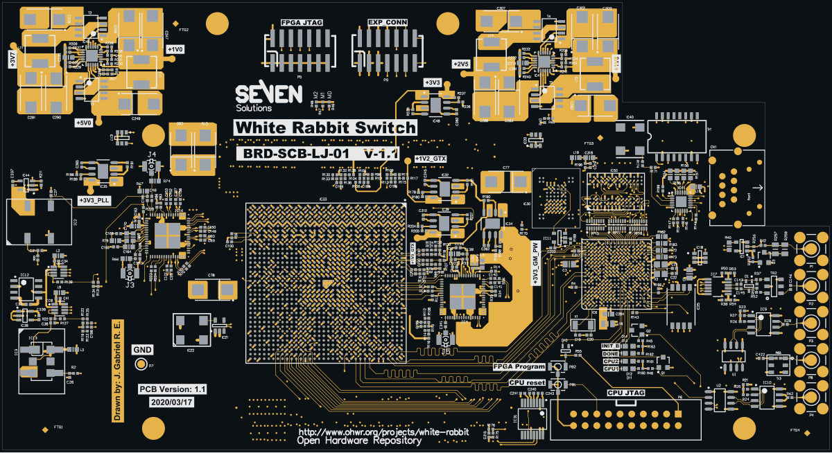
WRS LJ SCB (OHWR0053 R1) is an open-hardware circuit board from the CERN Open Hardware Repository, designed in Altium Designer: a 12-layer board of 180.6 × 97.8 mm with 667 components and 682 nets, published under CERN-OHL-1.2.
review 82% walked · 9 findings: 1 blocker · 5 major · 3 minor (19 items)
Open in the interactive viewerRead the full review
Design review
Probe recorded 9 findings: 1 blocker · 5 major · 3 minor (19 items) on this design. Each is shown here with its reasoning; the full review links every one to the pins, nets and datasheet pages it rests on.
- NetCopperSplitblockerOpen
GND_SHIELD's copper is in 2 pieces: C214.2 is not connected to the rest of the net
GND_SHIELD's copper is in 2 pieces: C214.2 is not connected to the rest of the net. Piece 1: CN1.0, on TOP_LAYER, MIDLAYER1, MIDLAYER2, MIDLAYER3, MIDLAYER4 and BOTTOM_LAYER, 1 drill(s), over (121.12, -20.3) to (128.42, -2.6). Piece 2: C214.2, on TOP_LAYER, MIDLAYER1, MIDLAYER2, MIDLAYER3, MIDLAYER4 and BOTTOM_LAYER, 1 drill(s), over (112.64, -4.3) to (131.5, 5.19). The export files every one of these pins under the net, so every connectivity check passes; the copper the fab builds leaves them apart. Usually a pour island that touches only one via of its own net, or a track ending short of its copper: join the piece to the net and export again.
At split:GND_SHIELD
ARM_PCK0: the ARM IC6 drives a 2.5 V clock (PA31/PCK0) straight into FPGA IC33 ball N33 in bank 15, which is powered at +1V8 (abs max 2.3 V)
Net ARM_PCK0 connects the AT91SAM9G45 IC6 ball V1 (PA31, whose peripheral-B function is the programmable clock PCK0) directly to Virtex-6 IC33 ball N33 (IO_L10P_MRCC_15). IC6 drives that line from VDDIOP0 = +2V5, while FPGA bank 15 has VCCO = +1V8. A 2.5 V high level exceeds the FPGA's absolute-maximum input voltage of VCCO + 0.5 V = 2.3 V.
Connection
End Pin Supply of that pin IC6 AT91SAM9G45 V1 = PA31 (MCI1_CK / PCK0) VDDIOP0 (PIO A table, p.25) = +2V5 on this board (balls K9/K10) IC33 XC6VLX130T N33 = IO_L10P_MRCC_15 Bank 15 VCCO = +1V8 There is no series resistor, divider or translator on ARM_PCK0 (two endpoints only).
``
mermaid graph LR ARM["IC6 PA31 / PCK0 (VDDIOP0 = +2V5)"] -->|ARM_PCK0, direct| FPGA["IC33 N33, bank 15 (VCCO = +1V8)"]``Limit vs actual
Quantity Limit Actual Margin FPGA VIN, bank 15 (DS152 abs max: -0.5 to VCCO + 0.5 V) 2.3 V about 2.5 V (ARM VOH at VDDIOP0 = 2.5 V, light load) -0.2 V The ARM EBI signals that share banks 15/16 are correctly at 1.8 V (VDDIOM1 = +1V8). This one PIO line comes from the 2.5 V peripheral domain. If PCK0 is enabled (the net name says it is meant to be), the FPGA input is driven about 0.2 V past its absolute maximum on every cycle, with the bank-15 input clamp conducting. Even as a plain PIO input with its reset pull-up enabled, the line idles at about 2.5 V.
Possible fixes
- Move ARM_PCK0 to a pin in a 2.5 V bank (banks 24/26/32/34/35 are +2V5), or
- add a series resistor plus divider, or a 2.5 V to 1.8 V translator, or
- take PCK0 from a VDDIOM1 or 1.8 V-powered alternative. PCK0 is also offered on PD12, PD26 and PE0, but those are in VDDIOP0/VDDANA/VDDIOP1, so a pin move on the FPGA side is simpler.
The sibling board OHWR0044 R1 WRS FL SCB has the same net on the same FPGA ball (N33, bank 15 at +1V8). It was not reported there.
IC47 (TPS53126) EN2, the enable of the +2V5 rail, is set by R61/R60 to about 1.91 V, below the guaranteed 2.0 V high threshold; before +1V0 is up it sits at 1.16 V, above the 0.3 V low threshold
The +2V5 rail (VCCAUX and most VCCO banks of FPGA IC33, the ARM IC6 VDDIOP, and the enable of every AP7173 LDO) is channel 2 of the TPS53126 IC47. Its EN2 pin is fed from a divider between +5VCC_IN (R61 9K31) and +1V0 (R60 2K8). With +1V0 up, EN2 settles at about 1.91 V, which is below the datasheet's minimum guaranteed high level of 2.0 V. With +1V0 still at 0 V, EN2 sits at about 1.16 V, which is above the maximum guaranteed low level of 0.3 V. Neither the "wait for +1V0" state nor the "on" state is guaranteed. Start-up depends on each part's actual threshold falling between 1.16 V and 1.91 V.
Circuit
``
mermaid graph LR V5["+5VCC_IN"] -->|R61 9K31| EN["IC47 pin 7 EN2"] V1["+1V0 (IC46 ch1)"] -->|R60 2K8| EN EN --> CH2["IC47 ch2 -> +2V5"] CH2 -->|+2V5 on EN1, pin 24| CH1["IC47 ch1 -> +1V8"] CH2 -->|EN of IC32/34/35/39/48| LDO["AP7173 LDOs: +3V3, +1V0_GTX, +1V2_GTX, +3V3_PLL, +3V3_PLL_GM"]``Limit vs actual
State EN2 voltage (Thevenin of R61/R60) TPS53126 limit (p.6) Margin +5VCC_IN = 5.0 V, +1V0 = 0 V (should be OFF) 5.0 x 2.8/(9.31+2.8) = 1.16 V VENL max 0.3 V -0.86 V (not guaranteed off) +5VCC_IN = 5.0 V, +1V0 = 0.97 V (should be ON) (5/9.31k + 0.97/2.8k)/(1/9.31k + 1/2.8k) = 1.91 V VENH min 2.0 V -0.09 V (not guaranteed on) +5VCC_IN = 5.25 V, +1V0 = 0.97 V 1.97 V VENH min 2.0 V -0.03 V +1V0 is IC46 channel 1, set by R230 2K8 / R231 10K to 0.758 V x 1.28 = 0.97 V.
Consequence
If EN2 does not reach this particular part's threshold, +2V5 never starts. Then +1V8 (IC47 EN1 is +2V5) and all five AP7173 rails also stay off, and the board does not power up. If the threshold is below 1.16 V, +2V5 starts together with +1V0, and the intended VCCINT-before-VCCAUX order is lost. That order is only DS152's recommendation, not a requirement. A divider that lands clearly above 2.0 V when +1V0 is present (for example a smaller R61, or EN2 derived from a +1V0 power-good), and clearly below 0.3 V when it is absent, would make this deterministic.
The companion channel IC46 EN1 uses R58/R57 4K7/4K7 from +5VCC_IN (2.5 V). That is inside spec and is not part of this finding.
- DecapOrdermajorOpen
DecapOrder: 4 findings (2 components, 2 pins)×4
e.g. “IC33 supply pins AA16, AA18, AB15, AB17, N14, N16, Y17, Y19 on '+1V0': the smallest capacitor C70 sits 3.6 mm away, behind C71 at 1.6 mm” · 4 different statements
At IC13.6, IC2.4, IC33
Each finding, with its own headline
IC13.6IC13 supply pin 6 on 'NetC40_1': the smallest capacitor C40 sits 3.4 mm away, behind C42 at 2.0 mm
IC13 supply pin 6 on 'NetC40_1': the smallest capacitor C40 sits 3.4 mm away, behind C42 at 2.0 mm. IC13.6: the smallest value, C40 (100 nF), is 3.4 mm from the pin and C42 (10 uF) 2.0 mm: the high-frequency part sits behind more inductance than the bulk part, which needs it least. Swap them, or bring the smallest value to the pin: it serves the fastest current and is the one the loop inductance defeats. Distances are pad centre to pin centre in the board plane. The 5 mm radius, the 10x value step and the 1 mm / 1.5x tie tolerance are Probe's starting values.
IC2.4IC2 supply pin 4 on '+3V3_VCO': the smallest capacitor C33 sits 4.7 mm away, behind C35 at 3.0 mm
IC2 supply pin 4 on '+3V3_VCO': the smallest capacitor C33 sits 4.7 mm away, behind C35 at 3.0 mm. IC2.4: the smallest value, C33 (100 nF), is 4.7 mm from the pin and C35 (10 uF) 3.0 mm: the high-frequency part sits behind more inductance than the bulk part, which needs it least. Swap them, or bring the smallest value to the pin: it serves the fastest current and is the one the loop inductance defeats. Distances are pad centre to pin centre in the board plane. The 5 mm radius, the 10x value step and the 1 mm / 1.5x tie tolerance are Probe's starting values.
IC33IC33 supply pins AA16, AA18, AB15, AB17, N14, N16, Y17, Y19 on '+1V0': the smallest capacitor C70 sits 3.6 mm away, behind C71 at 1.6 mm
IC33 supply pins AA16, AA18, AB15, AB17, N14, N16, Y17, Y19 on '+1V0': the smallest capacitor C70 sits 3.6 mm away, behind C71 at 1.6 mm. IC33.AA16: the smallest value, C70 (470 nF), is 3.6 mm from the pin and C71 (4.7 uF) 1.6 mm: the high-frequency part sits behind more inductance than the bulk part, which needs it least. IC33.AA18: the smallest value, C70 (470 nF), is 4.0 mm from the pin and C71 (4.7 uF) 0.7 mm: the high-frequency part sits behind more inductance than the bulk part, which needs it least. IC33.AB15: the smallest value, C70 (470 nF), is 4.7 mm from the pin and C71 (4.7 uF) 2.6 mm: the high-frequency part sits behind more inductance than the bulk part, which needs it least. IC33.AB17: the smallest value, C70 (470 nF), is 4.6 mm from the pin and C71 (4.7 uF) 0.8 mm: the high-frequency part sits behind more inductance than the bulk part, which needs it least. IC33.N14: the smallest value, C69 (470 nF), is 4.7 mm from the pin and C72 (4.7 uF) 1.6 mm: the high-frequency part sits behind more inductance than the bulk part, which needs it least. IC33.N16: the smallest value, C70 (470 nF), is 4.4 mm from the pin and C72 (4.7 uF) 2.0 mm: the high-frequency part sits behind more inductance than the bulk part, which needs it least. IC33.Y17: the smallest value, C70 (470 nF), is 2.7 mm from the pin and C71 (4.7 uF) 1.5 mm: the high-frequency part sits behind more inductance than the bulk part, which needs it least. IC33.Y19: the smallest value, C70 (470 nF), is 3.8 mm from the pin and C71 (4.7 uF) 2.1 mm: the high-frequency part sits behind more inductance than the bulk part, which needs it least. Swap them, or bring the smallest value to the pin: it serves the fastest current and is the one the loop inductance defeats. Distances are pad centre to pin centre in the board plane. The 5 mm radius, the 10x value step and the 1 mm / 1.5x tie tolerance are Probe's starting values.
IC33IC33 supply pins L32, M29 on '+1V8': the smallest capacitor C73 sits 4.1 mm away, behind C75 at 2.5 mm
IC33 supply pins L32, M29 on '+1V8': the smallest capacitor C73 sits 4.1 mm away, behind C75 at 2.5 mm. IC33.L32: the smallest value, C73 (470 nF), is 4.1 mm from the pin and C75 (22 uF) 2.5 mm: the high-frequency part sits behind more inductance than the bulk part, which needs it least. IC33.M29: the smallest value, C73 (470 nF), is 4.5 mm from the pin and C74 (4.7 uF) 0.6 mm: the high-frequency part sits behind more inductance than the bulk part, which needs it least. Swap them, or bring the smallest value to the pin: it serves the fastest current and is the one the loop inductance defeats. Distances are pad centre to pin centre in the board plane. The 5 mm radius, the 10x value step and the 1 mm / 1.5x tie tolerance are Probe's starting values.
- PartLifecyclemajorOpen
PartLifecycle: 6 part numbers×6
5 Obsolete, 1 Discontinued at DigiKey · on 10 placements
At IC13, IC21, IC6, IC7, T2, U1
Each finding, with its own headline
IC13YNETHE125 on IC13: the distributor catalogue reports "Obsolete" for Diodes Incorporated's YNETHE125
YNETHE125 on IC13: the distributor catalogue reports "Obsolete" for Diodes Incorporated's YNETHE125 — a sourcing/longevity risk to confirm against the MANUFACTURER before acting. This board's BOM names no manufacturer for it, so whether that is the fitted maker's product was not checked. A distributor delisting is not the same claim as the part being unavailable; check the vendor's own lifecycle/product-change notice for the status and any named successor. Re-read the source: GET /api/odb/parts/YNETHE125/providers (which provider said it, the maker and part number it matched, its own words, and when we asked). THE LAST BUY DATE HAS PASSED (2022-02-09, 1,740 day(s) ago), so this is a substitution rather than a buy. The distributor reports NONE left. No approved alternate is recorded for this position.
IC21DS90LV011ATMF on IC21: the distributor catalogue reports "Obsolete" for Texas Instruments's DS90LV011ATMF
DS90LV011ATMF on IC21: the distributor catalogue reports "Obsolete" for Texas Instruments's DS90LV011ATMF — a sourcing/longevity risk to confirm against the MANUFACTURER before acting. This board's BOM names National Semiconductor, and that is one line with Texas Instruments: Texas Instruments completed its acquisition of National Semiconductor on 2011-09-23. A distributor delisting is not the same claim as the part being unavailable; check the vendor's own lifecycle/product-change notice for the status and any named successor. Re-read the source: GET /api/odb/parts/DS90LV011ATMF/providers (which provider said it, the maker and part number it matched, its own words, and when we asked). THE LAST BUY DATE HAS PASSED (2025-04-10, 584 day(s) ago), so this is a substitution rather than a buy. The distributor reports 59,366 left. No approved alternate is recorded for this position.
IC6AT91SAM9G45-CU on IC6: the distributor catalogue reports "Obsolete" for Microchip Technology's AT91SAM9G45-CU
AT91SAM9G45-CU on IC6: the distributor catalogue reports "Obsolete" for Microchip Technology's AT91SAM9G45-CU — a sourcing/longevity risk to confirm against the MANUFACTURER before acting. This board's BOM names no manufacturer for it, so whether that is the fitted maker's product was not checked. A distributor delisting is not the same claim as the part being unavailable; check the vendor's own lifecycle/product-change notice for the status and any named successor. Re-read the source: GET /api/odb/parts/AT91SAM9G45-CU/providers (which provider said it, the maker and part number it matched, its own words, and when we asked). THE LAST BUY DATE HAS PASSED (2013-09-01, 4,823 day(s) ago), so this is a substitution rather than a buy. The distributor reports NONE left. No approved alternate is recorded for this position.
IC7LTC6957IMS-2#PBF on IC7: the distributor catalogue reports "Obsolete" for Analog Devices Inc.'s LTC6957IMS-2#PBF
LTC6957IMS-2#PBF on IC7: the distributor catalogue reports "Obsolete" for Analog Devices Inc.'s LTC6957IMS-2#PBF — a sourcing/longevity risk to confirm against the MANUFACTURER before acting. This board's BOM names no manufacturer for it, so whether that is the fitted maker's product was not checked. A distributor delisting is not the same claim as the part being unavailable; check the vendor's own lifecycle/product-change notice for the status and any named successor. Re-read the source: GET /api/odb/parts/LTC6957IMS-2#PBF/providers (which provider said it, the maker and part number it matched, its own words, and when we asked). THE LAST BUY DATE HAS PASSED (2025-01-17, 667 day(s) ago), so this is a substitution rather than a buy. The distributor reports NONE left. No approved alternate is recorded for this position.
T2IRF9910Pbf on 4 placements (T2, T3, T4, T5): the distributor catalogue reports "Discontinued at DigiKey" for Infineon Technologies's IRF9910PBF
IRF9910Pbf on 4 placements (T2, T3, T4, T5): the distributor catalogue reports "Discontinued at DigiKey" for Infineon Technologies's IRF9910PBF — a sourcing/longevity risk to confirm against the MANUFACTURER before acting. This board's BOM names INTERNATIONAL RECTIFIER, and that is one line with Infineon Technologies: Infineon completed its acquisitions of International Rectifier on 2015-01-13 and Cypress Semiconductor on 2020-04-16. A distributor delisting is not the same claim as the part being unavailable; check the vendor's own lifecycle/product-change notice for the status and any named successor. Re-read the source: GET /api/odb/parts/IRF9910Pbf/providers (which provider said it, the maker and part number it matched, its own words, and when we asked). No approved alternate is recorded for this position.
U1MC100LVEL51DG on 2 placements (U1, U2): the distributor catalogue reports "Obsolete" for onsemi's MC100LVEL51DG
MC100LVEL51DG on 2 placements (U1, U2): the distributor catalogue reports "Obsolete" for onsemi's MC100LVEL51DG — a sourcing/longevity risk to confirm against the MANUFACTURER before acting. This board's BOM names no manufacturer for it, so whether that is the fitted maker's product was not checked. A distributor delisting is not the same claim as the part being unavailable; check the vendor's own lifecycle/product-change notice for the status and any named successor. Re-read the source: GET /api/odb/parts/MC100LVEL51DG/providers (which provider said it, the maker and part number it matched, its own words, and when we asked). THE LAST BUY DATE HAS PASSED (2025-10-08, 403 day(s) ago), so this is a substitution rather than a buy. The distributor reports 42,457 left. No approved alternate is recorded for this position.
- SinglePointNetmajorOpen
SinglePointNet: 3 pins×3
3 checked by the review by Claude walker (cern session) — 3 different reasons
At IC31.10, IC33.F8, IC33.G8
Each finding, with its own headline
IC31.10IC31.10 (DIN2) is an IC input left unconnected
Pin IC31.10 (DIN2) is an IC INPUT left UNCONNECTED (on the no-connect bucket). Marked no-connect by the designer, but an input normally needs a defined level - confirm it is truly meant to float. If the datasheet defines this input left open (an internal pull, "read as low when left floating", or a tri-level input whose open state is one of its settings), file it on the pin as if_unused (pull_up, pull_down or may_float) with submit_pin_behavior, citing the page, and this finding clears.
IC33.F8IC33.F8 (CSI_B_0) is an IC input left unconnected
Pin IC33.F8 (CSI_B_0) is an IC INPUT left UNCONNECTED (on the no-connect bucket). Marked no-connect by the designer, but an input normally needs a defined level - confirm it is truly meant to float. If the datasheet defines this input left open (an internal pull, "read as low when left floating", or a tri-level input whose open state is one of its settings), file it on the pin as if_unused (pull_up, pull_down or may_float) with submit_pin_behavior, citing the page, and this finding clears.
IC33.G8IC33.G8 (RDWR_B_0) is an IC input left unconnected
Pin IC33.G8 (RDWR_B_0) is an IC INPUT left UNCONNECTED (on the no-connect bucket). Marked no-connect by the designer, but an input normally needs a defined level - confirm it is truly meant to float. If the datasheet defines this input left open (an internal pull, "read as low when left floating", or a tri-level input whose open state is one of its settings), file it on the pin as if_unused (pull_up, pull_down or may_float) with submit_pin_behavior, citing the page, and this finding clears.
TMP100 sensors IC17-IC20 run at +3V3, but their I2C bus (SCL_TMP/SDA_TMP) is pulled up to +2V5 by R128/R129: 0.19 V of VIH margin
The four TMP100 temperature sensors IC17, IC18, IC19 and IC20 are supplied from +3V3, while their I2C bus is pulled up to +2V5 and driven by the FPGA IC33 from a 2.5 V bank. The bus high level clears the sensors' input-high threshold by only 0.19 V at nominal rails, and falls below it at ±5 % rails.
What is wired
- Sensors IC17 to IC20 (TMP100): V+ (pin 4) on +3V3. SCL is pin 1, SDA is pin 6.
- Pull-ups R129 (SCL_TMP) and R128 (SDA_TMP): 10K to +2V5, both fitted.
- Master: FPGA IC33 balls G13 (IO_L0P_35, SCL_TMP) and H14 (IO_L0N_35, SDA_TMP), bank 35, VCCO = +2V5.
- No level translator on the bus.
``
mermaid graph LR FPGA["IC33 Virtex-6 bank 35 (VCCO +2V5)"] -->|SCL_TMP / SDA_TMP| S["IC17-IC20 TMP100 (V+ = +3V3, VIH = 0.7 x V+)"] PU["R128 / R129 10K"] -->|pull-up to +2V5| S``Limit vs actual
Condition TMP100 VIH min = 0.7 x (V+) (TI TMP100 datasheet p.5) Bus high level Margin Nominal rails 0.7 x 3.3 V = 2.31 V 2.5 V +0.19 V ±5 % rails (V+ 3.465 V, bus 2.375 V) 2.43 V 2.375 V -0.05 V At the tolerance corner the sensors are no longer guaranteed to read a logic 1 on SCL or SDA.
Why it is not trivially fixed
The TMP100 cannot move to the 2.5 V rail, because its supply range starts at 2.7 V (p.4). The robust fixes are a bidirectional I2C level shifter between the 2.5 V FPGA bank and a 3.3 V-pulled sensor bus, or the sensors on a supply low enough that 0.7 x V+ sits well under 2.5 V.
This is the same arrangement that was found on the sibling board OHWR0044 R1 WRS FL SCB (OBS-43); it was carried over unchanged to this board.
DataFlash IC25 (AT45DB641E) runs at +3V3 but its SI, SCK and CS inputs are driven from the ARM IC6's 2.5 V I/O: 0.19 V of VIH margin
The AT45DB641E DataFlash IC25 is supplied from +3V3, but its SI, SCK and CS inputs are driven directly by the AT91SAM9G45 IC6 on 2.5 V I/O with no translator, and CS is pulled up to +2V5. The flash's input-high threshold is 0.7 x VCC, so the margin is 0.19 V at nominal rails and becomes negative at ±5 % rails.
Connection
IC25 pin Net Driven by 1 (SI) SPI_SI IC6 ball V2 (PB1, SPI0_MOSI) 2 (SCK) SPI_SCK IC6 ball V3 (PB2, SPI0_SPCK) 4 (CS) SPI_CS IC6 ball U4 (PB3, SPI0_NPCS0); R166 10K pull-up to +2V5 6 (VCC) +3V3 IC6's PB0 to PB5 are powered by VDDIOP0 (AT91SAM9G45 datasheet PIO B multiplexing table, p.26), and VDDIOP0 (balls K9/K10) is on +2V5 on this board.
Margin
Case VIH min (0.7 x VCC, AT45DB641E p.59) Drive high Margin Nominal (VCC 3.3 V, drive 2.5 V) 2.31 V 2.50 V +0.19 V ±5 % (VCC 3.465 V, drive 2.375 V) 2.43 V 2.375 V -0.05 V ``
mermaid graph LR ARM["IC6 SAM9G45 PB1/PB2/PB3 (VDDIOP0 = +2V5)"] -->|SPI_SI / SPI_SCK / SPI_CS, no translator| DF["IC25 AT45DB641E (VCC = +3V3, VIH = 0.7 x VCC)"] DF -->|SO via R250 100R / R1 330R divider| ARM``The return direction is handled: SO (pin 8) comes back through the R250/R1 divider to about 2.5 V. The forward direction is not. The same arrangement was found on the sibling board OHWR0044 R1 WRS FL SCB (OBS-57), and it recurs here. It shares its cause with the TMP100 bus finding on this board (OBS-134): 3.3 V parts on a 2.5 V-driven bus.
- ConnectorDomainMixedminorOpen
P9 takes 3 different supplies off the board on one connector: +5VCC_IN (5.0 V), +3V3 (3.307 V), +2V5 (2.549 V)
P9 carries 3 different supplies out of the board on one connector: +5VCC_IN (5.0 V) on 5, +3V3 (3.307 V) on 3, +2V5 (2.549 V) on 1. Declare the intent. Two rails on one connector is ordinary in a docking or power-distribution interface and a hazard in a signal one, and the difference is not visible from the netlist — but note that adjacent contacts at different voltages are exactly what a mirrored, reversed or off-by-one cable shorts together, so the cost of getting the mating wrong is a rail collision rather than a dead signal. If this is a standard connector, declare its family (connector_family_declare) and file the standard's contact map: supplies on the contacts it assigns to power are then not reported.
At P9
Main parts
| Part number | Maker | Description | Where |
|---|---|---|---|
| 7M-12.000MAAJ-T | SMD Crystal 7M Series 18pF 30 ppm | X2 | |
| ABS09-32.768KHZ-T | Raltron | Crystal Oscillator 12pF | X1 |
| AT45DB641E | 64-megabit 2.7V, Dual-Interface DataFlash | IC25 | |
| AT91SAM9G45-CU | Atmel 400MHz ARM926 MCU | IC6 | |
| DOT050V-020.0M | VCXO Ultra-Low Phase Noise Oscillator | IC2 | |
| DS90LV011ATMF | National Semiconductor | Single High Speed Differential Driver | IC21 |
| Header 10X2 | Sullis Connectors | Header, 10-Pin, Dual row, 2.54mm pitch | P6 |
| IS43DR16320E-25DBLI | DDR2 SDRAM 8Mx16x4 Banks | IC50 | |
| LAN8720A-CP | SMSC | RMII ethernet transceiver with auto MIDIX | IC41 |
| LTC6957IMS-2#PBF | Low Phase Noise, Dual LVDS Output Buffer/Driver/Logic Converter | IC7 | |
| MAX3232CDBR | IC31 | ||
| MT29F4G16ABCHC | NAND Flash 256Mx16, 1.8V Asynch/Page | IC30 | |
| Plug | Plug | P7 | |
| REF5030AID | TEXAS INSTRUMENTS | Low-Noise, Very Low Drift, Precision Voltage Reference | IC12 |
| SN74LVC1G125DBVR | TI 2.5V single tri-state buffer | IC1 | |
| SN74LVC1G32 | TI single OR gate | IC11 | |
| TR_H1260NL | ethernet trafo (TME) | Tr1 | |
| Tyco 1888250-1 | low profile uTCA Ethernet jack (RJ45) | CN1 | |
| WBC1-1LB | Coilcraft | SMT Mini WideBand Transformer 1:1, 10uH, | Tr3 |
| WBC16-1TLB | COILCRAFT | SMT Transformer WBC Series Type B Pinout | TR2 |
| XC6VLX130T-1FF1156C | Virtex-6 LXT Platform FPGA, 600 User I/Os, 20 GTXs, 1156-Ball FFBGA, Speed Grade 1, Commercial Grade | IC33 | |
| YNETHE125 | VCXO 3.3V 125 MHz CMOS Oscillator | IC13 | |
| AD5662B | Analog Devices 16-bit DAC w/SPI interface, ext ref | IC5, IC8 | |
| AD9516-4BCPZ | PLL with clock fanout | IC16, IC4 | |
| FNETHE025 | SMD oscillator 3.3V (Elfa) | IC22, IC40 | |
| Header 7X2 | Header, 7-Pin, Dual row, 2.0 mm pitch | P5, P9 | |
| ICS83023I | 350MHz Differential-to-LVCMOS Translator/Buffer | IC10, IC9 | |
| LT1761ES5-3.3#TRPBF | LINEAR TECHNOLOGY | 100mA, Low Noise, LDO Micropower Regulator in SOT-23 | IC38, IC44 |
| MC100LVEL51DG | Differential Clock D-Type Flip-Flop | U1, U2 | |
| PB_OMRON_B3U-1100P | OMRON | Push-Button Switch SPDT | PB1, PB2 |
| QSS-048-01-L-D-DP | [NoValue], High Speed Ground Plane Header | J1, J2 | |
| TPS53126RGET | TEXAS INSTRUMENTS | Dual Synchronous Step-Down Controller For Low Voltage Power Rails | IC46, IC47 |
| BAT6804WH6327XTSA1 | Dual Series RF Schottky Barrier Diodes | D1, D10, D15 | |
| NDS331N | N-Channel Logic Level Enhancement Mode Field Effect Transistor | Q1, Q2, Q3 | |
| IRF9910Pbf | INTERNATIONAL RECTIFIER | Dual SO-8 MOSFET For POL Cconverter | T2, T3, T4, T5 |
| LED | Typical INFRARED GaAs LED | D11, D12, D13, D14 | |
| TMP100 | I2C temp. sensor | IC17, IC18, IC19, IC20 | |
| AP7173-SPG-13 | 1.5A Low Dropout Linera Regulator | IC32, IC34, IC35, IC39, IC48 | |
| SMC | SMB Straight Connector | P1, P2, P3, P4, P8 | |
| 27R x 8 | 27R, 62.5mW Chip Resistor 8 Elements Array | RP15, RP16, RP17, RP18, RP19, RP20 |
About this design
- Design
- WRS LJ SCB — OHWR0053 R1
- Designed in
- Altium Designer
- Board
- 12 copper layers, 180.6 × 97.8 mm, 667 components, 682 nets
- Licence
- CERN-OHL-1.2
- Source
- https://gitlab.com/ohwr/project/wrs-lj-hw at commit
dbcb74816e2b - Attribution
- CERN Open Hardware Repository, project ohwr/project/wrs-lj-hw (commit dbcb74816e2beebb87f59c88827ce344b8d7ea12, 2025-04-10). Licence: CERN-OHL-1.2. Source: https://gitlab.com/ohwr/project/wrs-lj-hw. This is a snapshot of the copy published on the OHWR GitLab pages (R1), not CERN's released record. CERN's source of truth is EDMS (https://edms.cern.ch), and the current release may be newer.
- Reviewed with
- Probe by E# (E-Sharp AB)