 Probe

WRS LJ WRITE HO 01
OHWR0054 · revision R1
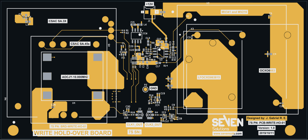
WRS LJ WRITE HO 01 (OHWR0054 R1) is an open-hardware circuit board from the CERN Open Hardware Repository, designed in Altium Designer: a 4-layer board of 142.4 × 64.3 mm with 69 components and 40 nets, published under CERN-OHL-1.2.
review 87% walked · 12 findings: 2 blocker · 4 major · 6 minor (14 items)
Open in the interactive viewerRead the full review
Design review
Probe recorded 12 findings: 2 blocker · 4 major · 6 minor (14 items) on this design. Each is shown here with its reasoning; the full review links every one to the pins, nets and datasheet pages it rests on.
- NetCopperSplitblockerOpen
10MHZ_SINE's copper is in 2 pieces: C9.2 is not connected to the rest of the net
10MHZ_SINE's copper is in 2 pieces: C9.2 is not connected to the rest of the net. Piece 1: X1.5, X2.3 and X3.5, on TOP_LAYER and BOTTOM_LAYER, 3 drill(s), 50.48 mm2 of pour, over (79.18, 10.68) to (88.25, 17.8). Piece 2: C9.2, on TOP_LAYER, over (74.19, 10.52) to (79.86, 11.44). The export files every one of these pins under the net, so every connectivity check passes; the copper the fab builds leaves them apart. Usually a pour island that touches only one via of its own net, or a track ending short of its copper: join the piece to the net and export again.
At split:10MHZ_SINE
- CapVoltageDeratingblockerOpen
CapVoltageDerating: 2 components×2
2 checked by the review by evaluation@esharp.se — 2 different reasons
At C10, C4
Each finding, with its own headline
C10C10 is rated 6.3 V on a 12 V rail
C10: rated 6.3 V on a 12 V rail — UNDER-rated.
C4C4 is rated 6.3 V on a 12 V rail
C4: rated 6.3 V on a 12 V rail — UNDER-rated.
- SinglePointNetmajorOpen
'10MHZ_CMOS' reaches only IC5.2
Net '10MHZ_CMOS' is EFFECTIVELY single-point: it is wired to 4 pins but only one is POPULATED - the other connection(s) are DNP (X5.12, X6.3, X4.4). The populated end IC5.2 is an IC INPUT, so as built it FLOATS. Confirm the depopulation is intended and the input has a defined level another way. If the datasheet defines this input left open (an internal pull, "read as low when left floating", or a tri-level input whose open state is one of its settings), file it on the pin as if_unused (pull_up, pull_down or may_float) with submit_pin_behavior, citing the page, and this finding clears.
At 10MHZ_CMOS
- FloatingInputmajorOpen
IC5.2 on '10MHZ_CMOS' has no driver and no pull
Net '10MHZ_CMOS': input(s) IC5.2 with no driver and no pull — floating input (undefined level); add a driver or a pull resistor.
At 10MHZ_CMOS
- ReferencePlaneDiscontinuitymajorOpen
ReferencePlaneDiscontinuity: 2 boards×2
e.g. “12 nets change reference between +3V3 and GND at 13 vias, none with a reference that continues across (fastest: DAC_DIN at 100 ps 10-90 %, ASSUMED)” · 2 different statements
At refchange:+3V3|GND, refchange:+5V|GND
Each finding, with its own headline
refchange:+3V3|GND12 nets change reference between +3V3 and GND at 13 vias, none with a reference that continues across (fastest: DAC_DIN at 100 ps 10-90 %, ASSUMED)
At 13 via(s), on 12 net(s), the signal leaves a layer referenced by one of +3V3 and GND for a layer referenced by the other, and no plane references both layers. Different nets: no via can carry the return across; only decoupling between the two planes near the via can. The capacitor carrying the return across was measured at each via, at the knee of the crossing net's edge against 50 ohm assumed: 13 with none. 13 of them at an ASSUMED edge (no edge on file for the net): state one (net_timing_state) and it is re-read. One decision covers the pair: whether +3V3 and GND are decoupled to each other near these vias. A via whose layers have more references than these two is a site of each pair it joins. None is partial: at every one, no reference continues across the via.
- 'VCTROL_+5V0' at (75.87, 38.92), TOP_LAYER -> BOTTOM_LAYER: GND on GND to +3V3 on PWR; pure, no reference continues across; stitching none, 97.5 mm of track past the via on BOTTOM_LAYER: At the 5 GHz knee of a 100 ps edge (20 ns 10-90 %, assumed: no edge is on file for the net) no capacitor carries the return; only the planes do. +3V3 and GND are not a thin pair (at most 0.2 mm), so their own capacitance does not carry the return. To serve it, change layers across the same plane, or move the signal to a layer referenced to ground. None.
- 'VCTROL_+3V0' at (70.1, 31.72), TOP_LAYER -> BOTTOM_LAYER: GND on GND to +3V3 on PWR; pure, no reference continues across; stitching none, 54.8 mm of track past the via on BOTTOM_LAYER: At the 5 GHz knee of a 100 ps edge (20 ns 10-90 %, assumed: no edge is on file for the net) no capacitor carries the return; only the planes do. +3V3 and GND are not a thin pair (at most 0.2 mm), so their own capacitance does not carry the return. To serve it, change layers across the same plane, or move the signal to a layer referenced to ground. None.
- 'VCTROL_+10V0' at (64.02, 41.42), TOP_LAYER -> BOTTOM_LAYER: GND on GND to +3V3 on PWR; pure, no reference continues across; stitching none, 47.1 mm of track past the via on BOTTOM_LAYER: At the 5 GHz knee of a 100 ps edge (20 ns 10-90 %, assumed: no edge is on file for the net) no capacitor carries the return; only the planes do. +3V3 and GND are not a thin pair (at most 0.2 mm), so their own capacitance does not carry the return. To serve it, change layers across the same plane, or move the signal to a layer referenced to ground. None.
- 'VCTROL_+2V5' at (64.72, 33.1), TOP_LAYER -> BOTTOM_LAYER: GND on GND to +3V3 on PWR; pure, no reference continues across; stitching none, 29.6 mm of track past the via on BOTTOM_LAYER: At the 5 GHz knee of a 100 ps edge (20 ns 10-90 %, assumed: no edge is on file for the net) no capacitor carries the return; only the planes do. +3V3 and GND are not a thin pair (at most 0.2 mm), so their own capacitance does not carry the return. To serve it, change layers across the same plane, or move the signal to a layer referenced to ground. None.
- 'TMP_SCL' at (63.4, 12.73), TOP_LAYER -> BOTTOM_LAYER: GND on GND to +3V3 on PWR; pure, no reference continues across; stitching none, 17.0 mm of track past the via on BOTTOM_LAYER: At the 5 GHz knee of a 100 ps edge (10 ns 10-90 %, assumed: no edge is on file for the net) no capacitor carries the return; only the planes do. +3V3 and GND are not a thin pair (at most 0.2 mm), so their own capacitance does not carry the return. To serve it, change layers across the same plane, or move the signal to a layer referenced to ground. None.
- 'TMP_SDA' at (63.37, 15.53), TOP_LAYER -> BOTTOM_LAYER: GND on GND to +3V3 on PWR; pure, no reference continues across; stitching none, 15.6 mm of track past the via on BOTTOM_LAYER: At the 5 GHz knee of a 100 ps edge (10 ns 10-90 %, assumed: no edge is on file for the net) no capacitor carries the return; only the planes do. +3V3 and GND are not a thin pair (at most 0.2 mm), so their own capacitance does not carry the return. To serve it, change layers across the same plane, or move the signal to a layer referenced to ground. None.
- 'NetIC3_3' at (55.8, 35.05), TOP_LAYER -> BOTTOM_LAYER: GND on GND to +3V3 on PWR; pure, no reference continues across; stitching none, 9.9 mm of track past the via on BOTTOM_LAYER: At the 5 GHz knee of a 100 ps edge (100 ps 10-90 %, assumed: no edge is on file for the net) no capacitor carries the return; only the planes do. +3V3 and GND are not a thin pair (at most 0.2 mm), so their own capacitance does not carry the return. To serve it, change layers across the same plane, or move the signal to a layer referenced to ground. None.
- 'NetIC3_3' at (64.22, 35.68), TOP_LAYER -> BOTTOM_LAYER: GND on GND to +3V3 on PWR; pure, no reference continues across; stitching none, 9.9 mm of track past the via on BOTTOM_LAYER: At the 5 GHz knee of a 100 ps edge (100 ps 10-90 %, assumed: no edge is on file for the net) no capacitor carries the return; only the planes do. +3V3 and GND are not a thin pair (at most 0.2 mm), so their own capacitance does not carry the return. To serve it, change layers across the same plane, or move the signal to a layer referenced to ground. None.
- 'DAC_SCLK' at (57, 23.98), TOP_LAYER -> BOTTOM_LAYER: GND on GND to +3V3 on PWR; pure, no reference continues across; stitching none, 3.4 mm of track past the via on BOTTOM_LAYER: At the 5 GHz knee of a 100 ps edge (1 ns 10-90 %, assumed: no edge is on file for the net) no capacitor carries the return; only the planes do. +3V3 and GND are not a thin pair (at most 0.2 mm), so their own capacitance does not carry the return. To serve it, change layers across the same plane, or move the signal to a layer referenced to ground. None.
- 'FPGA_RX' at (55.05, 23.95), TOP_LAYER -> BOTTOM_LAYER: GND on GND to +3V3 on PWR; pure, no reference continues across; stitching none, 3.3 mm of track past the via on BOTTOM_LAYER: At the 5 GHz knee of a 100 ps edge (3 ns 10-90 %, assumed: no edge is on file for the net) no capacitor carries the return; only the planes do. +3V3 and GND are not a thin pair (at most 0.2 mm), so their own capacitance does not carry the return. To serve it, change layers across the same plane, or move the signal to a layer referenced to ground. None.
- 'FPGA_TX' at (53.05, 23.97), TOP_LAYER -> BOTTOM_LAYER: GND on GND to +3V3 on PWR; pure, no reference continues across; stitching none, 3.3 mm of track past the via on BOTTOM_LAYER: At the 5 GHz knee of a 100 ps edge (3 ns 10-90 %, assumed: no edge is on file for the net) no capacitor carries the return; only the planes do. +3V3 and GND are not a thin pair (at most 0.2 mm), so their own capacitance does not carry the return. To serve it, change layers across the same plane, or move the signal to a layer referenced to ground. None.
- 'DAC_SYNC' at (55.08, 13.18), TOP_LAYER -> BOTTOM_LAYER: GND on GND to +3V3 on PWR; pure, no reference continues across; stitching none, 3.3 mm of track past the via on BOTTOM_LAYER: At the 5 GHz knee of a 100 ps edge (100 ps 10-90 %, assumed: no edge is on file for the net) no capacitor carries the return; only the planes do. +3V3 and GND are not a thin pair (at most 0.2 mm), so their own capacitance does not carry the return. To serve it, change layers across the same plane, or move the signal to a layer referenced to ground. None.
- and 1 more
Every site is a row of this finding's evidence, keyed by net, layers and position. GET /api/odb/boards/55/reference-planes?group=refchange%3A%2B3V3%7CGND serves each with its own layer_image region; all of them lie in x 51.05..77.87, y 10.73..43.42 mm (board frame, Y up).
The reference on each layer is the first plane the track meets leaving the via, anti-pads and the net's own copper skipped. Whether it matters depends on each signal's edge rate, which nothing on file states for these nets: a slow static line crosses a split harmlessly, a fast edge does not.
refchange:+5V|GND'VCTROL_+3V0' changes reference between +5V and GND at a via, none with a reference that continues across (fastest: VCTROL_+3V0 at 20 ns 10-90 %, suggested by its name)
At 1 via(s), on 1 net(s), the signal leaves a layer referenced by one of +5V and GND for a layer referenced by the other, and no plane references both layers. Different nets: no via can carry the return across; only decoupling between the two planes near the via can. The capacitor carrying the return across was measured at each via, at the knee of the crossing net's edge against 50 ohm assumed: 1 with none. 1 of them at an ASSUMED edge (no edge on file for the net): state one (net_timing_state) and it is re-read. One decision covers the pair: whether +5V and GND are decoupled to each other near these vias. A via whose layers have more references than these two is a site of each pair it joins. None is partial: at every one, no reference continues across the via.
- 'VCTROL_+3V0' at (19.23, 34.2), TOP_LAYER -> BOTTOM_LAYER: GND on GND to +5V on PWR; pure, no reference continues across; stitching none, 54.8 mm of track past the via on BOTTOM_LAYER: At the 5 GHz knee of a 100 ps edge (20 ns 10-90 %, assumed: no edge is on file for the net) no capacitor carries the return; only the planes do. +5V and GND are not a thin pair (at most 0.2 mm), so their own capacitance does not carry the return. To serve it, change layers across the same plane, or move the signal to a layer referenced to ground. None.
Every site is a row of this finding's evidence, keyed by net, layers and position. GET /api/odb/boards/55/reference-planes?group=refchange%3A%2B5V%7CGND serves each with its own layer_image region; all of them lie in x 17.23..21.23, y 32.2..36.2 mm (board frame, Y up).
The reference on each layer is the first plane the track meets leaving the via, anti-pads and the net's own copper skipped. Whether it matters depends on each signal's edge rate, which nothing on file states for these nets: a slow static line crosses a split harmlessly, a fast edge does not.
- FiducialMissingmajorOpen
The top side carries 61 SMT component(s) and no fiducial was found on it
The top side carries 61 SMT component(s) but no fiducial was found on it — a placement machine has no optical reference to align to. Probe found no pad labelled .pad_usage=g_fiducial/l_fiducial (basis pad_usage); no single-pad, netless, undrilled component whose 0.5-3 mm round pad has a concentric solder-mask opening at least 1.5x its diameter with no other copper inside it (basis geometry); and no component whose refdes starts FID or whose part or package name contains FIDUCIAL (basis footprint-name). If your library names fiducials something Probe does not recognise, mark this benign — disposition_finding(rule='FiducialMissing', entity='top', status='benign', reason=…) — the name match only ever silences this check, it never asserts anything. If the side really has no fiducial, say so with status='confirmed': that answers the finding and keeps it gating release.
At top
TMP100 sensor IC4 runs at +3V3, but its I2C bus (TMP_SCL/TMP_SDA) is pulled up to +2V5 by R15/R16: 0.19 V of VIH margin
Temperature sensor IC4 (TMP100 in the schematic, TMP101NA in the BOM value) is supplied from +3V3. Its I2C bus is pulled up to +2V5 by R15/R16 (4k7) and is driven by the SCB's FPGA from a 2.5 V bank through P1. At nominal rails the bus high level clears the sensor's input-high threshold by only 0.19 V, and at ±5 % rails it falls below the threshold.
What is wired
- IC4 V+ (pin 4) is on +3V3. SCL is pin 1 (TMP_SCL) and SDA is pin 6 (TMP_SDA).
- R15 (TMP_SCL) and R16 (TMP_SDA) are 4k7 pull-ups to +2V5, taken from P1 pin 2. Both are fitted. There is no other pull-up on this board or on the SCB side.
- P1 pins 8 and 10 mate the SCB's P9 pins 7 and 9 (HO_FPGA_EXP6/EXP5). Those go to the FPGA IC33 balls F19/E21, in the bank whose VCCO (A22) is +2V5.
- There is no level translator.
``
mermaid graph LR FPGA["SCB IC33 Virtex-6, VCCO +2V5"] -->|HO_FPGA_EXP6/5 via P9 to P1| BUS["TMP_SCL / TMP_SDA"] PU["R15 / R16 4k7 to +2V5"] --> BUS BUS --> S["IC4 TMP100 (V+ = +3V3, VIH = 0.7 x V+)"]``Limit vs actual
Condition TMP100 VIH min = 0.7 x (V+) (datasheet p.5) Bus high level Margin Nominal rails 0.7 x 3.3 V = 2.31 V 2.5 V +0.19 V ±5 % rails (V+ 3.465 V, bus 2.375 V) 2.43 V 2.375 V -0.05 V At the tolerance corner, IC4 is no longer guaranteed to see a logic 1 on SCL or SDA.
Notes
- The TMP100 cannot move to +2V5, because its supply range starts at 2.7 V (p.3/p.4). A bidirectional level shifter, or sensor pull-ups to +3V3 with a translator to the 2.5 V bank, would fix it.
- The TMP101 variant named in the BOM value has the same VIH (the datasheet covers both).
- The SCB's own TMP100 bus has the same arrangement (OBS-134).
REF5030 IC6 is fed from +3V3 through L6: 107 mV above its 3.2 V minimum input at nominal, below it at the regulator's tolerance corner
The DAC reference IC6 (REF5030AID, 3.0 V) takes its input (pin 2) from +3V3 through ferrite L6. The REF5030 needs at least VOUT + 0.2 V = 3.2 V. +3V3 comes from the SCB's AP7173 LDO (IC48), which is set to 3.307 V nominal and rated ±2 %. At nominal the headroom is 107 mV. At the LDO's own tolerance it is 41 mV, and with the 1 % feedback resistors added it goes negative (about 3.19 V). Below 3.2 V the reference is outside its recommended operating range, and the DAC full scale (the OCXO steering voltage) then follows the +3V3 rail instead of the reference.
What sits between what
``
mermaid graph LR LDO["SCB IC48 AP7173, 0.8 V x (1 + 4K7/1K5) = 3.307 V, ±2 %"] -->|+3V3 via SCB P9 pin 3 / P1 pin 4| L6["L6 BLM18KG221SN1D"] L6 -->|NetC21_2, C21 1 uF| REF["IC6 REF5030AID VIN (pin 2), needs VOUT + 0.2 V"] REF -->|+3V0_REFDAC| DAC["IC3 AD5662 VREF (pin 2)"]`` The same P1 pin 4 also carries +3V3 for IC3, IC4, U1, IC1/IC2/IC5 and, through L1, the +3V3_OCXO supply of whichever 3.3 V oscillator option (X3, X4 or X5) is fitted. Any drop across the connector and ferrites comes out of this headroom too.Limit vs actual
Case +3V3 at IC6 VIN REF5030 VIN min (VOUT + 0.2 V, p.5) Margin Nominal divider, nominal VREF 3.307 V 3.200 V +107 mV AP7173 accuracy -2 % (p.1/p.5) 3.241 V 3.200 V +41 mV -2 % and R237 -1 % / R236 +1 % about 3.192 V 3.200 V -8 mV Connector, trace and ferrite drops under oscillator load are not included, and they only reduce the figures.
Notes
- The datasheet asks for 'a supply of 200mV more than the output voltage in an unloaded condition' (p.26-27). Typical dropout at the ~1 mA load here is lower, so a typical board will work. The concern is the guaranteed corner, on a reference whose only job is a stable steering voltage during holdover.
- A 5 V input (P1 pin 6, +5V) would give the REF5030 1.8 V of headroom. The SCB's own REF5030 takes a dedicated LDO rail (+3AV3, LT1761, 3.23 V minimum).
No global fiducials on the WRITE hold-over board, top or bottom, although it carries a 0.5 mm-pitch DFN (U1) and SC-70 logic
The board has no fiducial marks on either side. Automated pick-and-place therefore has no board-level reference unless the assembler adds panel fiducials. The top side carries fine-pitch SMT: U1 5PB1213 in a 10-pin DFN, IC2/IC5 NC7SZ04 in SC-70-5, IC3 AD5662 in SOT-23-8, and two U.FL receptacles. The bottom side carries the SMD 2x7 socket P1.
What was checked
- Placement/ODB: no pad with a fiducial usage attribute, and no FID* refdes or FIDUCIAL part, on either side. The BOM has no fiducial rows.
- Copper, paste, mask and silk renders of the whole top side (12.6 px/mm) and the corners (50 px/mm): the round features at the board corners are mounting-hole mask openings with no copper dot, and the small white dots are silk pin-1 markers.
- Bottom side: only P1 and its routing.
Side SMT parts Fiducials found Needed (common practice: 2-3 global per side with SMT) Top 62 fitted SMT parts, finest 0.5 mm-pitch DFN (U1) 0 2-3 Bottom P1 (2 mm-pitch SMD socket) 0 2-3, or panel fiducials Why it matters
Without fiducials the machine aligns to the board edge or tooling holes, and the placement error grows with the distance from them. On a 142 x 64 mm board that is marginal for a 0.5 mm-pitch DFN. It can be recovered at panelisation (panel fiducials), which is why this is minor.
DAC IC3 drives op-amp U2 inputs directly: if +12V0 (J1) is absent while the SCB rails are up, U2's input limits ((V+)+0.5 V, ±10 mA) are exceeded
The board has two independent supplies: +3V3/+2V5/+5V arrive from the SCB on P1, and +12V0 arrives on its own connector J1 and feeds op-amp U2 (via L4, +VAMP) and the 12 V OCXO options X1/X2 (via L2). Nothing sequences them. The DAC IC3 is powered from +3V3, and its output (up to 3.0 V) connects straight to U2's non-inverting inputs (pins 3 and 5) with no series resistor. If J1 is unpowered while the SCB runs and the gateware has written a non-zero code, U2's inputs sit above (V+) + 0.5 V. The only current limit is the DAC output: 30 mA short-circuit typical, against U2's ±10 mA input-current rating.
What sits between what
``
mermaid graph LR SCB["SCB +3V3 via P1"] --> L5["L5"] --> DAC["IC3 AD5662 VOUT (0-3.0 V), no series R"] DAC --> INP["U2 OPA2180 +INA (3) / +INB (5)"] J1["J1 +12V0 (external, may be absent)"] --> L4["L4"] --> VAMP["+VAMP = U2 V+ (8)"] J1 --> L2["L2"] --> OCXO["+12V_OCXO: X1 / X2 option"] INP -. "input protection path when V+ = 0" .-> VAMP``Limit vs actual (J1 unpowered, DAC at a mid-to-full-scale code)
Quantity Limit (OPA2180 abs max, p.8) Actual Margin Input voltage (V+) + 0.5 V = 0.5 V with +VAMP at 0 V up to 3.0 V exceeded Input current ±10 mA limited only by the DAC output (short-circuit current 30 mA typ, AD5662 p.3) and by whatever back-powered +VAMP/+12V0 load draws exceeded when a 12 V OCXO (X1/X2) is fitted, because its load then hangs off the back-powered +12V0 through L4/L2 With no 12 V oscillator fitted, the back-powered load is only U2 (525 uA max quiescent, p.1) plus C10/C11, so the current stays small, but the voltage limit is still exceeded.
Notes
- Whether the system can ever run the SCB with J1 unpowered is a system fact not recorded here. If J1 and the SCB always share one supply that comes up together, the exposure is limited to the ramp.
- A series resistor of about 1 kOhm in each U2 input (inside the high-impedance, zero-drift input's error budget) would cap the fault current below 3 mA.
- ConnectorDomainMixedminorOpen
P1 takes 3 different supplies off the board on one connector: +5V (5.0 V), +3V3 (3.307 V), +2V5 (2.549 V)
P1 carries 3 different supplies out of the board on one connector: +5V (5.0 V) on 6, +3V3 (3.307 V) on 4, +2V5 (2.549 V) on 2. Declare the intent. Two rails on one connector is ordinary in a docking or power-distribution interface and a hazard in a signal one, and the difference is not visible from the netlist — but note that adjacent contacts at different voltages are exactly what a mirrored, reversed or off-by-one cable shorts together, so the cost of getting the mating wrong is a rail collision rather than a dead signal. If this is a standard connector, declare its family (connector_family_declare) and file the standard's contact map: supplies on the contacts it assigns to power are then not reported.
At P1
- FiducialMissingminorOpen
The bottom side carries 1 SMT component(s) and no fiducial was found on it
The bottom side carries 1 SMT component(s) but no fiducial was found on it — a placement machine has no optical reference to align to. Probe found no pad labelled .pad_usage=g_fiducial/l_fiducial (basis pad_usage); no single-pad, netless, undrilled component whose 0.5-3 mm round pad has a concentric solder-mask opening at least 1.5x its diameter with no other copper inside it (basis geometry); and no component whose refdes starts FID or whose part or package name contains FIDUCIAL (basis footprint-name). If your library names fiducials something Probe does not recognise, mark this benign — disposition_finding(rule='FiducialMissing', entity='bottom', status='benign', reason=…) — the name match only ever silences this check, it never asserts anything. If the side really has no fiducial, say so with status='confirmed': that answers the finding and keeps it gating release. Graded minor: the side carries only 1 SMT part(s) (at most 5), which a placement machine can usually align on their own pads; a fine-pitch part among them would still want one.
At bottom
Main parts
| Part number | Maker | Description | Where |
|---|---|---|---|
| 5PB1213 | Clock buffer 1:3 LVCMOS/Sine | U1 | |
| AD5662B | Analog Devices 16-bit DAC w/SPI interface, ext ref | IC3 | |
| CON2_THT2.54mm | Connector | J1 | |
| Header 7X2 | Header, 7-Pin, Dual row, 2.0 mm pitch | P1 | |
| OPA2180 | Zero-Drift, Low Noise, Rail-to-Rail Input/Output, 36V Operational Amplifier | U2 | |
| Plug | Plug | P2 | |
| REF5030AID | TEXAS INSTRUMENTS | Low-Noise, Very Low Drift, Precision Voltage Reference | IC6 |
| SN74LVC1G125DBVR | TI 2.5V single tri-state buffer | IC1 | |
| TMP100 | I2C temp. sensor | IC4 | |
| NC7SZ04P5X | TinyLogic® HS Inverter | IC2, IC5 | |
| U.FL-R-SMT-1(10) | Up to 6GHz Ultra Small Surface Mount Male Coaxial Connectors U.FL Series | J2, J3 | |
| R0402_100R_1%_0.0625W_100PPM | GENERIC | Resistor - 1% | R1 |
| R0402_10K_1%_0.0625W_100PPM | GENERIC | Resistor - 1% | R3, R5 |
| R0402_33R_1%_0.0625W_100PPM | GENERIC | Resistor - 1% | R18, R4 |
| R0402_1K_1%_0.0625W_100PPM | GENERIC | Resistor - 1% | R12, R19, R8 |
| R0402_330R_1%_0.0625W_100PPM | GENERIC | Resistor - 1% | R10, R11, R2 |
| R0402_220R_1%_0.0625W_100PPM | GENERIC | Resistor - 1% | R13, R14, R17, R9 |
| R0402_4K7_1%_0.0625W_100PPM | GENERIC | Resistor - 1% | R15, R16, R6, R7 |
| BLM18KG221SN1D | Murata | ferrite bead | L1, L2, L3, L4, L6 |
| CC0603_1UF_25V_10%_X7R | GENERIC | Non-polarised capacitor | C13, C16, C17, C18, C21 |
| CC0603_10uF_6.3V_20%_X5R | GENERIC | Non-polarised capacitor | C10, C14, C2, C22, C4, C6 |
| CC0402_100NF_16V_10%_X7R | GENERIC | Non-polarised capacitor | C1, C11, C12, C20, C23, C24 and 6 more |
About this design
- Design
- WRS LJ WRITE HO 01 — OHWR0054 R1
- Designed in
- Altium Designer
- Board
- 4 copper layers, 142.4 × 64.3 mm, 69 components, 40 nets
- Licence
- CERN-OHL-1.2
- Source
- https://gitlab.com/ohwr/project/wrs-lj-hw at commit
dbcb74816e2b - Attribution
- CERN Open Hardware Repository, project ohwr/project/wrs-lj-hw (commit dbcb74816e2beebb87f59c88827ce344b8d7ea12, 2025-04-10). Licence: CERN-OHL-1.2. Source: https://gitlab.com/ohwr/project/wrs-lj-hw. This is a snapshot of the copy published on the OHWR GitLab pages (R1), not CERN's released record. CERN's source of truth is EDMS (https://edms.cern.ch), and the current release may be newer.
- Reviewed with
- Probe by E# (E-Sharp AB)