 Probe

WRS V2 AMC SFP
OHWR0015 · revision R1
WRS V2 AMC SFP (OHWR0015 R1) is an open-hardware circuit board from the CERN Open Hardware Repository, designed in Altium Designer: a 4-layer board of 180.6 × 73.5 mm with 49 components and 41 nets, published under CERN-OHL-1.2.
review 90% walked · 9 findings: 1 blocker · 6 major · 2 minor (12 items)
Open in the interactive viewerRead the full review
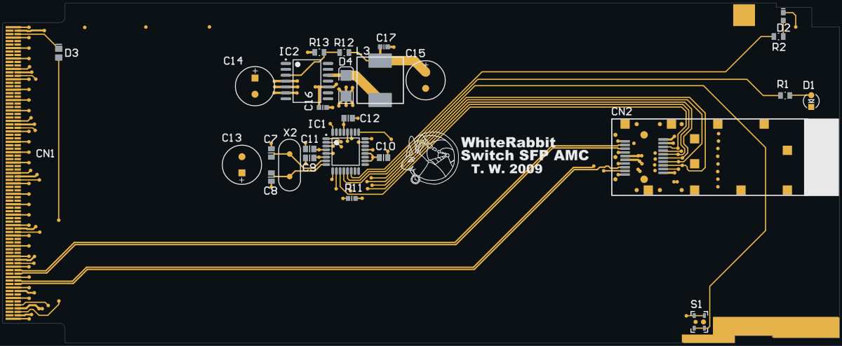
Design review
Probe recorded 9 findings: 1 blocker · 6 major · 2 minor (12 items) on this design. Each is shown here with its reasoning; the full review links every one to the pins, nets and datasheet pages it rests on.
- CapVoltageDeratingblockerOpen
C14 is rated 10 V on a 12 V rail
C14: rated 10 V on a 12 V rail — UNDER-rated.
At C14
AMC SFP buck IC2 LM2574 uses a standard-recovery rectifier (D4 MRA4006T3G) as its catch diode
The catch diode D4 of the AMC SFP buck IC2 (LM2574) is an MRA4006T3G, a standard-recovery rectifier, where the LM2574 datasheet calls for a Schottky or fast-recovery type.
Where it is
D4 is the freewheeling diode of the 52 kHz LM2574 buck that makes +3V3 from the AMC 12 V payload power: cathode (pin 2) on the switch node NetD4_2 (IC2 pin 12 OUTPUT, L3 330 uH), anode (pin 1) on GND.
What the datasheets say
Part Fact Source MRA4006T3G 1 A standard-recovery power rectifier, intended for line-frequency rectification MRA4006T3G datasheet, p.1 LM2574 catch diode Schottky, or fast-recovery high-efficiency types; standard 60 Hz rectifiers are not suitable LM2574 datasheet, p.17 Why it matters
A standard-recovery diode conducts in reverse for microseconds at every switch turn-on, adding switching loss in D4 and the LM2574 switch and raising noise and temperature.
Note: the page-12 evidence row attached at creation (60-Hz ripple on ON/OFF) is not relevant to this finding; the page-17 row is the citation.
The published AMC SFP BOM mounts both halves of the R9/R10 '0*' option pair, which shorts +3V3 to GND through SFP pin 7
The published AMC SFP BOM mounts both halves of the R9/R10 '0*' option pair, which shorts +3V3 to GND through SFP pin 7 (NetCN2_7).
Where it is
Part Pin 1 Pin 2 R9, 0 Ohm GND NetCN2_7 (CN2 pin 7, the SFP cage's rate-select contact) R10, 0 Ohm +3V3 NetCN2_7 The schematic marks both '0*', the same assembly-option convention as on the MCH boards, and only one should be fitted.
The BOM row
BOM CSV row 'R9, R10': Name '0*', Value 0, LibRef R0603_0R_JUMPER, Mounted 'Yes'. An assembler following it shorts +3V3 to GND.
For this review both are treated as not fitted.
- PartLifecyclemajorOpen
ATmega8L-8AC on IC1: the distributor catalogue reports "Obsolete" for Microchip Technology's ATMEGA8L-8AC
ATmega8L-8AC on IC1: the distributor catalogue reports "Obsolete" for Microchip Technology's ATMEGA8L-8AC — a sourcing/longevity risk to confirm against the MANUFACTURER before acting. This board's BOM names no manufacturer for it, so whether that is the fitted maker's product was not checked. A distributor delisting is not the same claim as the part being unavailable; check the vendor's own lifecycle/product-change notice for the status and any named successor. Re-read the source: GET /api/odb/parts/ATmega8L-8AC/providers (which provider said it, the maker and part number it matched, its own words, and when we asked). THE LAST BUY DATE HAS PASSED (2007-12-31, 6,894 day(s) ago), so this is a substitution rather than a buy. The distributor reports NONE left. No approved alternate is recorded for this position.
At IC1
- FiducialMissingmajorOpen
FiducialMissing: 2 boards×2
Checked by the review, stands · Claude walker (cern session) — No fiducial component on this board: the BOM has no FID*/FTG*/fiducial row and the rule found no fiducial-attribute pad on either side. Not refuted; whether fiducials are carried on the production panel instead is for the owner.
At bottom, top
Each finding, with its own headline
bottomThe bottom side carries 22 SMT component(s) and no fiducial was found on it
The bottom side carries 22 SMT component(s) but no fiducial was found on it — a placement machine has no optical reference to align to. Probe found no pad labelled .pad_usage=g_fiducial/l_fiducial (basis pad_usage); no single-pad, netless, undrilled component whose 0.5-3 mm round pad has a concentric solder-mask opening at least 1.5x its diameter with no other copper inside it (basis geometry); and no component whose refdes starts FID or whose part or package name contains FIDUCIAL (basis footprint-name). If your library names fiducials something Probe does not recognise, mark this benign — disposition_finding(rule='FiducialMissing', entity='bottom', status='benign', reason=…) — the name match only ever silences this check, it never asserts anything. If the side really has no fiducial, say so with status='confirmed': that answers the finding and keeps it gating release.
topThe top side carries 22 SMT component(s) and no fiducial was found on it
The top side carries 22 SMT component(s) but no fiducial was found on it — a placement machine has no optical reference to align to. Probe found no pad labelled .pad_usage=g_fiducial/l_fiducial (basis pad_usage); no single-pad, netless, undrilled component whose 0.5-3 mm round pad has a concentric solder-mask opening at least 1.5x its diameter with no other copper inside it (basis geometry); and no component whose refdes starts FID or whose part or package name contains FIDUCIAL (basis footprint-name). If your library names fiducials something Probe does not recognise, mark this benign — disposition_finding(rule='FiducialMissing', entity='top', status='benign', reason=…) — the name match only ever silences this check, it never asserts anything. If the side really has no fiducial, say so with status='confirmed': that answers the finding and keeps it gating release.
- PartLifecyclemajorOpen
LM2574M-ADJ on IC2: the distributor catalogue reports "Obsolete" for Texas Instruments's LM2574M-ADJ
LM2574M-ADJ on IC2: the distributor catalogue reports "Obsolete" for Texas Instruments's LM2574M-ADJ — a sourcing/longevity risk to confirm against the MANUFACTURER before acting. This board's BOM names National Semiconductor, and that is one line with Texas Instruments: Texas Instruments completed its acquisition of National Semiconductor on 2011-09-23. A distributor delisting is not the same claim as the part being unavailable; check the vendor's own lifecycle/product-change notice for the status and any named successor. Re-read the source: GET /api/odb/parts/LM2574M-ADJ/providers (which provider said it, the maker and part number it matched, its own words, and when we asked). THE LAST BUY DATE HAS PASSED (2024-09-11, 795 day(s) ago), so this is a substitution rather than a buy. The distributor reports NONE left. No approved alternate is recorded for this position.
At IC2
- ReferencePlaneDiscontinuitymajorOpen
ReferencePlaneDiscontinuity: 2 boards×2
Checked by the review, stands · Claude walker W2 (Cern session) — Checked: the crossings and reference changes are read from the copper and stand as stated. No edge-rate or impedance requirement on file makes them a defect: most nets involved are slow control/IO, and the stackup's stated planes give a nearby return for most crossings as reported. Layout practice, left for the owner.
At gap:SUPPLY:hole 10.49,-23.85|49.63,-23.6, gap:SUPPLY:hole 44.76,-15.09|53.39,-6.45
Each finding, with its own headline
gap:SUPPLY:hole 10.49,-23.85|49.63,-23.62 nets cross one gap in SUPPLY's negative-plane field at 2 places, the longest 0.36 mm (fastest: NetCN1_3 at 100 ps 10-90 %, ASSUMED)
Along 'UTCA_GA0' on BOTTOM_LAYER, SUPPLY is a negative layer (copper everywhere inside the profile), and its field is cleared for 0.36 mm under the track at (10.54, -23.72). The layer does not state the nets either side, so whether this is a split between two planes or a void in one is not said; either way the return current has to go round it. 2 places on 2 net(s) cross it, listed below, the longest first. What cleared it: the hole at x 10.49..49.63, y -23.85..-23.6. One decision covers the void: whether these tracks may cross it, or the plane should be filled under them. No crossing has a plane on the track's other side, so the whole return meets the break.
- 'UTCA_GA0' on BOTTOM_LAYER at (10.54, -23.72), 0.36 mm; other side: none: the signal layer is outermost
- 'NetCN1_3' on BOTTOM_LAYER at (11.46, -23.72), 0.25 mm; other side: none: the signal layer is outermost
Every site is a row of this finding's evidence, keyed by net, layers and position. GET /api/odb/boards/18/reference-planes?group=gap%3ASUPPLY%3Ahole%2010.49%2C-23.85%7C49.63%2C-23.6 serves each with its own layer_image region; all of them lie in x 9.54..12.46, y -24.98..-22.6 mm (board frame, Y up).
Read from the copper as drawn on the reference layer, along each track's centreline at exact breakpoints. The reference is the copper beside the track, never the layer's type or name. Whether it matters depends on each signal's edge rate, which nothing on file states for these nets: a slow static line crosses a split harmlessly, a fast edge does not.
gap:SUPPLY:hole 44.76,-15.09|53.39,-6.453 nets cross one gap in SUPPLY's negative-plane field at 3 places, the longest 0.36 mm (fastest: UTCA_GA0 at 100 ps 10-90 %, ASSUMED)
Along 'UTCA_GA1' on BOTTOM_LAYER, SUPPLY is a negative layer (copper everywhere inside the profile), and its field is cleared for 0.36 mm under the track at (46.25, -7.95). The layer does not state the nets either side, so whether this is a split between two planes or a void in one is not said; either way the return current has to go round it. 3 places on 3 net(s) cross it, listed below, the longest first. What cleared it: the hole at x 44.76..53.39, y -15.09..-6.45. One decision covers the void: whether these tracks may cross it, or the plane should be filled under them. No crossing has a plane on the track's other side, so the whole return meets the break.
- 'UTCA_GA0' on BOTTOM_LAYER at (46.86, -8.56), 0.36 mm; other side: none: the signal layer is outermost
- 'UTCA_GA1' on BOTTOM_LAYER at (46.25, -7.95), 0.36 mm; other side: none: the signal layer is outermost
- 'UTCA_GA2' on BOTTOM_LAYER at (45.42, -7.11), 0.36 mm; other side: none: the signal layer is outermost
Every site is a row of this finding's evidence, keyed by net, layers and position. GET /api/odb/boards/18/reference-planes?group=gap%3ASUPPLY%3Ahole%2044.76%2C-15.09%7C53.39%2C-6.45 serves each with its own layer_image region; all of them lie in x 44.24..48.04, y -9.56..-6.11 mm (board frame, Y up).
Read from the copper as drawn on the reference layer, along each track's centreline at exact breakpoints. The reference is the copper beside the track, never the layer's type or name. Whether it matters depends on each signal's edge rate, which nothing on file states for these nets: a slow static line crosses a split harmlessly, a fast edge does not.
- ConnectorDomainMixedminorOpen
CN1 takes 2 different supplies off the board on one connector: +12V (12.0 V), +3V3_MP (3.3 V)
CN1 carries 2 different supplies out of the board on one connector: +12V (12.0 V) on 18/2/27/42/57/72/84/9, +3V3_MP (3.3 V) on 4. Declare the intent. Two rails on one connector is ordinary in a docking or power-distribution interface and a hazard in a signal one, and the difference is not visible from the netlist — but note that adjacent contacts at different voltages are exactly what a mirrored, reversed or off-by-one cable shorts together, so the cost of getting the mating wrong is a rail collision rather than a dead signal. If this is a standard connector, declare its family (connector_family_declare) and file the standard's contact map: supplies on the contacts it assigns to power are then not reported.
At CN1
- ReferencePlaneDiscontinuityminorOpen
ReferencePlaneDiscontinuity: 2 boards×2
Checked by the review, stands · Claude walker W2 (Cern session) — Checked: the crossings and reference changes are read from the copper and stand as stated. No edge-rate or impedance requirement on file makes them a defect: most nets involved are slow control/IO, and the stackup's stated planes give a nearby return for most crossings as reported. Layout practice, left for the owner.
At gap:SUPPLY:hole 44.76,6.86|49.45,11.56, gap:SUPPLY:hole 58.34,11.3|60.17,13.13
Each finding, with its own headline
gap:SUPPLY:hole 44.76,6.86|49.45,11.562 nets cross one gap in SUPPLY's negative-plane field at 2 places, the longest 0.36 mm (fastest: UTCA_SCL_L at 10 ns 10-90 %, suggested by its name)
Along 'UTCA_ENABLE' on BOTTOM_LAYER, SUPPLY is a negative layer (copper everywhere inside the profile), and its field is cleared for 0.36 mm under the track at (46.12, 8.23). The layer does not state the nets either side, so whether this is a split between two planes or a void in one is not said; either way the return current has to go round it. 2 places on 2 net(s) cross it, listed below, the longest first. What cleared it: the hole at x 44.76..49.45, y 6.86..11.56. One decision covers the void: whether these tracks may cross it, or the plane should be filled under them. No crossing has a plane on the track's other side, so the whole return meets the break.
- 'UTCA_ENABLE' on BOTTOM_LAYER at (46.12, 8.23), 0.36 mm; other side: none: the signal layer is outermost
- 'UTCA_SCL_L' on BOTTOM_LAYER at (47.73, 9.83), 0.36 mm; other side: none: the signal layer is outermost
Every site is a row of this finding's evidence, keyed by net, layers and position. GET /api/odb/boards/18/reference-planes?group=gap%3ASUPPLY%3Ahole%2044.76%2C6.86%7C49.45%2C11.56 serves each with its own layer_image region; all of them lie in x 44.94..48.91, y 7.23..10.83 mm (board frame, Y up).
Read from the copper as drawn on the reference layer, along each track's centreline at exact breakpoints. The reference is the copper beside the track, never the layer's type or name. Whether it matters depends on each signal's edge rate, which nothing on file states for these nets: a slow static line crosses a split harmlessly, a fast edge does not.
gap:SUPPLY:hole 58.34,11.3|60.17,13.13'UTCA_SDA_L' crosses one gap in SUPPLY's negative-plane field at 1 place, the longest 0.36 mm (fastest: UTCA_SDA_L at 10 ns 10-90 %, suggested by its name)
Along 'UTCA_SDA_L' on BOTTOM_LAYER, SUPPLY is a negative layer (copper everywhere inside the profile), and its field is cleared for 0.36 mm under the track at (59.49, 12.45). The layer does not state the nets either side, so whether this is a split between two planes or a void in one is not said; either way the return current has to go round it. What cleared it: the hole at x 58.34..60.17, y 11.3..13.13. One decision covers the void: whether these tracks may cross it, or the plane should be filled under them. No crossing has a plane on the track's other side, so the whole return meets the break.
- 'UTCA_SDA_L' on BOTTOM_LAYER at (59.49, 12.45), 0.36 mm; other side: none: the signal layer is outermost
Every site is a row of this finding's evidence, keyed by net, layers and position. GET /api/odb/boards/18/reference-planes?group=gap%3ASUPPLY%3Ahole%2058.34%2C11.3%7C60.17%2C13.13 serves each with its own layer_image region; all of them lie in x 58.31..60.67, y 11.45..13.45 mm (board frame, Y up).
Read from the copper as drawn on the reference layer, along each track's centreline at exact breakpoints. The reference is the copper beside the track, never the layer's type or name. Whether it matters depends on each signal's edge rate, which nothing on file states for these nets: a slow static line crosses a split harmlessly, a fast edge does not.
Main parts
| Part number | Maker | Description | Where |
|---|---|---|---|
| 1n4148 | Schottky Diode | D3 | |
| ATmega8L-8AC | 8-Bit AVR Microcontroller with 8K Bytes of In-System Programmable Flash Memory | IC1 | |
| HLMP-1700 | AVAGO TECHNOLOGIES | LED Red 1C 2A | D1 |
| LED | Chip LED (any color) | D2 | |
| LM2574M-ADJ | National Semiconductor | SIMPLE SWITCHER 0.5A Step-Down Voltage Regulator | IC2 |
| MRA4006T3G | Schottky Diode | D4 | |
| UTCA_AMC_TONGUE1 | AMC1.0 connector | CN1 | |
| uTCA_HS | Push button | S1 | |
| R0805_10K_1%_0.125W_100PPM | GENERIC | Resistor - 1% | R13 |
| R0805_16K9_0.1%_0.1W_10PPM | GENERIC | Resistor - 0.1% | R12 |
| CC0805_22PF_50V_5%_NP0 | GENERIC | Non-polarised capacitor | C7, C8 |
| R0805_330R_1%_0.125W_100PPM | GENERIC | Resistor - 1% | R1, R2 |
| 10SP100M | SANYO | Polarised capacitor | C13, C14, C15 |
| CC1206_10uF_10V_10%_X7R | GENERIC | Non-polarised capacitor | C1, C3, C5 |
| CC0805_100NF_50V_10%_X7R | GENERIC | Non-polarised capacitor | C10, C11, C12, C9 |
| CC0603_100NF_50V_10%_X7R | GENERIC | Non-polarised capacitor | C16, C17, C2, C4, C6 |
| R1206_100K_1%_0.25W_100PPM | GENERIC | Resistor - 1% | R14, R15, R16, R17, R18, R19 |
| R0603_10K_1%_0.1W_100PPM | GENERIC | Resistor - 1% | R11, R3, R4, R5, R6, R7, R8 |
About this design
- Design
- WRS V2 AMC SFP — OHWR0015 R1
- Designed in
- Altium Designer
- Board
- 4 copper layers, 180.6 × 73.5 mm, 49 components, 41 nets
- Licence
- CERN-OHL-1.2
- Source
- https://gitlab.com/ohwr/project/wr-switch-hw at commit
54f8a604978b - Attribution
- CERN Open Hardware Repository, project ohwr/project/wr-switch-hw (commit 54f8a604978bdc65bbde5b1f4c7ec9bee3505a44, 2025-04-09). Licence: CERN-OHL-1.2. Source: https://gitlab.com/ohwr/project/wr-switch-hw. This is a snapshot of the copy published on the OHWR GitLab pages (R1), not CERN's released record. CERN's source of truth is EDMS (https://edms.cern.ch), and the current release may be newer.
- Reviewed with
- Probe by E# (E-Sharp AB)