 Probe

WRS V2 MCH CLKB
OHWR0016 · revision R1
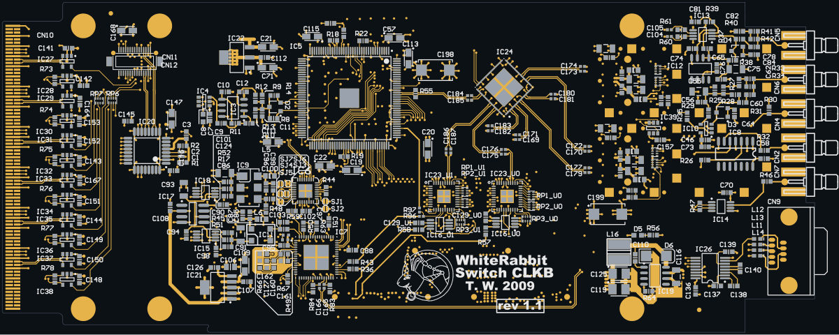
WRS V2 MCH CLKB (OHWR0016 R1) is an open-hardware circuit board from the CERN Open Hardware Repository, designed in Altium Designer: a 6-layer board of 180.6 × 73.5 mm with 421 components and 434 nets, published under CERN-OHL-1.2.
review 74% walked · 18 findings: 10 major · 8 minor (64 items)
Open in the interactive viewerRead the full review
Design review
Probe recorded 18 findings: 10 major · 8 minor (64 items) on this design. Each is shown here with its reasoning; the full review links every one to the pins, nets and datasheet pages it rests on.
TMP101 fitted on a TMP100 layout (CLKB): IC41 would share 0x48 with the ADN4600, IC39 and IC42 would share 0x49, and IC41/IC42 ALERT outputs are tied to +3V3
IC39-IC42 are ordered as TMP101 on a TMP100 layout: with TMP101s fitted, IC41 collides with the ADN4600 IC24 at 0x48, IC39 and IC42 share 0x49, and the IC41/IC42 ALERT outputs are tied to +3V3.
Where it is
The BOM row for IC39-IC42 reads Name 'TMP100', Value 'TMP101NA/250', LibRef 'TMP100'. The straps follow the TMP100 two-pin scheme (pin 3 ADD1, pin 5 ADD0). All sensors share the SCL/SDA bus with IC24 and the FPGA IC5.
Part Pin 3 Pin 5 (ADD0) Address as TMP100 Address as TMP101 IC24 ADN4600 ADDR1 (pin 50) GND ADDR0 (pin 49) GND 0x48 0x48 IC39 GND open 0x49 0x49 IC40 GND +3V3 0x4A 0x4A IC41 +3V3 GND 0x4C 0x48, collides with IC24; ALERT tied to +3V3 IC42 +3V3 open 0x4D 0x49, collides with IC39; ALERT tied to +3V3 Sources: netlist; TMP100 datasheet p.3 (on the TMP101 pin 3 is ALERT, an open-drain output; on the TMP100 it is ADD1) and p.10 (the TMP101 has a single address pin, ADD0); ADN4600 datasheet p.22 (slave address 10010 followed by ADDR1, ADDR0).
With a TMP100 fitted the bus is correct. On a TMP101, IC41/IC42 would sink +3V3 through ALERT when it asserts.
Why it matters
The FPGA (IC5) configures the ADN4600 and reads the sensors over this one bus. A collision with the crosspoint corrupts its configuration writes as well as the temperature reads.
AD8541 IC12 is wired with a dual-op-amp pinout: its real output (pin 6) is unconnected and pins 1-2 are shorted, so the VBB buffer for the MC100EP16 input bias drives nothing
AD8541 IC12 is wired with a dual-op-amp pinout: its real output (pin 6) is unconnected and pins 1-2 are shorted, so the VBB buffer that biases the MC100EP16 (IC13) input drives nothing.
Pin by pin
IC12 pin AD8541 function (SOIC-8) Board net 1 NC NetC75_2 (with C75, C76, R37, R38) 2 -IN NetC75_2 3 +IN EXT_VBB, from IC13 MC100EP16 VBB (IC13.4) 4 V- GND 5 NC 6 OUT unconnected 7 V+ +3V3 8 NC Tying pins 1 and 2 together is the follower pattern of a dual op-amp, where OUTA is pin 1.
What follows
``
mermaid flowchart LR VBB["IC13 VBB<br/>EXT_VBB"] --> IN["IC12 pin 3 +IN"] OUT["IC12 pin 6 OUT"] -.- NC["unconnected"] N["NetC75_2<br/>pins 1-2, no driver<br/>held only by C75 / C76"] --> R37["R37 10k"] --> P3["IC13 pin 3"] N --> R38["R38 10k"] --> P2["IC13 pin 2"]``With pin 1 a no-connect, NetC75_2 has no driver: the loop is open, the output saturates unloaded, and the bias node that R37 and R38 feed into IC13 pins 3 and 2 is held only by C75/C76. The receiver's input common mode is therefore undefined.
Why it matters
The EP16 receives the external reference input; without a defined bias it may not switch cleanly or at all on an AC-coupled input. An AD8542 (dual, pin 1 = OUTA) or re-routing pin 6 to NetC75_2 would match the intent.
- DecapOrdermajorOpen
DecapOrder: 3 findings (2 pins, 1 component)×3
Checked by the review, stands · Claude walker W2 (Cern session) — Checked: the distances are read from placement and stand as stated. Which capacitor sits nearest a supply pin at the 1-5 mm scale is a layout heuristic (Probe's starting thresholds), not a requirement of the part's datasheet on file; at this scale via and plane-spreading inductance usually dominate. Left for the owner.
At IC16_U0.6, IC23_U0.6, IC23_U1
Each finding, with its own headline
IC16_U0.6IC16_U0 supply pin 6 on '+2V5': the smallest capacitor C131_U0 sits 3.6 mm away, behind C129_U0 at 2.3 mm
IC16_U0 supply pin 6 on '+2V5': the smallest capacitor C131_U0 sits 3.6 mm away, behind C129_U0 at 2.3 mm. IC16_U0.6: the smallest value, C131_U0 (10 nF), is 3.6 mm from the pin and C129_U0 (100 nF) 2.3 mm: the high-frequency part sits behind more inductance than the bulk part, which needs it least. Swap them, or bring the smallest value to the pin: it serves the fastest current and is the one the loop inductance defeats. Distances are pad centre to pin centre in the board plane. The 5 mm radius, the 10x value step and the 1 mm / 1.5x tie tolerance are Probe's starting values.
IC23_U0.6IC23_U0 supply pin 6 on '+2V5': the smallest capacitor C131_U0 sits 3.4 mm away, behind C128_U0 at 0.8 mm
IC23_U0 supply pin 6 on '+2V5': the smallest capacitor C131_U0 sits 3.4 mm away, behind C128_U0 at 0.8 mm. IC23_U0.6: the smallest value, C131_U0 (10 nF), is 3.4 mm from the pin and C128_U0 (100 nF) 0.8 mm: the high-frequency part sits behind more inductance than the bulk part, which needs it least. Swap them, or bring the smallest value to the pin: it serves the fastest current and is the one the loop inductance defeats. Distances are pad centre to pin centre in the board plane. The 5 mm radius, the 10x value step and the 1 mm / 1.5x tie tolerance are Probe's starting values.
IC23_U1IC23_U1 supply pins 16, 37 on '+2V5': the smallest capacitor C130_U1 sits 3.4 mm away, behind C133_U1 at 0.8 mm
IC23_U1 supply pins 16, 37 on '+2V5': the smallest capacitor C130_U1 sits 3.4 mm away, behind C133_U1 at 0.8 mm. IC23_U1.16: the smallest value, C130_U1 (10 nF), is 3.4 mm from the pin and C133_U1 (100 nF) 0.8 mm: the high-frequency part sits behind more inductance than the bulk part, which needs it least. IC23_U1.37: the smallest value, C131_U1 (10 nF), is 3.0 mm from the pin and C158_U1 (100 nF) 1.1 mm: the high-frequency part sits behind more inductance than the bulk part, which needs it least. Swap them, or bring the smallest value to the pin: it serves the fastest current and is the one the loop inductance defeats. Distances are pad centre to pin centre in the board plane. The 5 mm radius, the 10x value step and the 1 mm / 1.5x tie tolerance are Probe's starting values.
- DecapViaFanoutmajorOpen
DecapViaFanout: 2 components×2
Checked by the review, stands · Claude walker W2 (Cern session) — Checked: the fanout length is read from the copper and stands; 0.5 nH is Probe's starting value, not a datasheet requirement. Whether it matters depends on the rail's PDN target, which is not stated. Left for the owner.
At C112, C33
Each finding, with its own headline
C112C112 on '+1V2': its rail pad reaches its via over 5.27 mm of track and its ground pad over 1.16 mm, adding about 2.24 nH to its loop, past Probe's 0.5 nH starting value; put the vias at the pads
C112 on '+1V2': its rail pad reaches its via over 5.27 mm of track and its ground pad over 1.16 mm, adding about 2.24 nH to its loop, past Probe's 0.5 nH starting value; put the vias at the pads. C112.2 (rail) runs 5.27 mm along its copper to its nearest via, 4.27 mm past the 1 mm beside the pad: 2.16 nH; C112.1 (ground) runs 1.16 mm along its copper to its nearest via, 0.16 mm past the 1 mm beside the pad: 0.08 nH. Each run past the pad as one conductor of a pair 1.60 mm apart (the pad pitch), 0.2 l ln(D/R) nH with R 0.127 mm (the track's width is not read): 2.24 nH in all. Put the vias at the pads (or in them), one per pad at least, the rail's and the ground's close together; the capacitor's own inductance as mounted is 1.26 nH (pad 0.10 nH + no via of the first net within 1 mm of its pad: the study's 0.6 nH per mm of 1.08 mm depth, ASSUMED). 0.5 nH is Probe's starting value, about the whole mounted inductance of a well-mounted 0402.
C33C33 on '+2V5': its rail pad reaches its via over 1.03 mm of track and its ground pad over 3.00 mm, adding about 1.03 nH to its loop, past Probe's 0.5 nH starting value; put the vias at the pads
C33 on '+2V5': its rail pad reaches its via over 1.03 mm of track and its ground pad over 3.00 mm, adding about 1.03 nH to its loop, past Probe's 0.5 nH starting value; put the vias at the pads. C33.1 (rail) runs 1.03 mm along its copper to its nearest via, 0.03 mm past the 1 mm beside the pad: 0.02 nH; C33.2 (ground) runs 3.00 mm along its copper to its nearest via, 2.00 mm past the 1 mm beside the pad: 1.01 nH. Each run past the pad as one conductor of a pair 1.60 mm apart (the pad pitch), 0.2 l ln(D/R) nH with R 0.127 mm (the track's width is not read): 1.03 nH in all. Put the vias at the pads (or in them), one per pad at least, the rail's and the ground's close together; the capacitor's own inductance as mounted is 1.42 nH (pad 0.10 nH + no via of the first net within 1 mm of its pad: the study's 0.6 nH per mm of 1.35 mm depth, ASSUMED). 0.5 nH is Probe's starting value, about the whole mounted inductance of a well-mounted 0402.
- FiducialMissingmajorOpen
FiducialMissing: 2 boards×2
Checked by the review, stands · Claude walker (cern session) — No fiducial component in this board's BOM (no FID*/FTG*/fiducial row) and no fiducial-attribute pad found by the rule. Not refuted; whether the panel carries them is for the owner.
At bottom, top
Each finding, with its own headline
bottomThe bottom side carries 111 SMT component(s) and no fiducial was found on it
The bottom side carries 111 SMT component(s) but no fiducial was found on it — a placement machine has no optical reference to align to. Probe found no pad labelled .pad_usage=g_fiducial/l_fiducial (basis pad_usage); no single-pad, netless, undrilled component whose 0.5-3 mm round pad has a concentric solder-mask opening at least 1.5x its diameter with no other copper inside it (basis geometry); and no component whose refdes starts FID or whose part or package name contains FIDUCIAL (basis footprint-name). If your library names fiducials something Probe does not recognise, mark this benign — disposition_finding(rule='FiducialMissing', entity='bottom', status='benign', reason=…) — the name match only ever silences this check, it never asserts anything. If the side really has no fiducial, say so with status='confirmed': that answers the finding and keeps it gating release.
topThe top side carries 243 SMT component(s) and no fiducial was found on it
The top side carries 243 SMT component(s) but no fiducial was found on it — a placement machine has no optical reference to align to. Probe found no pad labelled .pad_usage=g_fiducial/l_fiducial (basis pad_usage); no single-pad, netless, undrilled component whose 0.5-3 mm round pad has a concentric solder-mask opening at least 1.5x its diameter with no other copper inside it (basis geometry); and no component whose refdes starts FID or whose part or package name contains FIDUCIAL (basis footprint-name). If your library names fiducials something Probe does not recognise, mark this benign — disposition_finding(rule='FiducialMissing', entity='top', status='benign', reason=…) — the name match only ever silences this check, it never asserts anything. If the side really has no fiducial, say so with status='confirmed': that answers the finding and keeps it gating release.
- FloatingInputmajorOpen
FloatingInput: 8 nets×8
e.g. “IC24.10 on 'XIN2_P' has no driver and no pull” · 8 different statements
At XIN0_N, XIN0_P, XIN1_N, XIN1_P, XIN2_N, XIN2_P, XIN3_N, XIN3_P
Each finding, with its own headline
XIN0_NIC24.6 on 'XIN0_N' has no driver and no pull
Net 'XIN0_N': input(s) IC24.6 with no driver and no pull — floating input (undefined level); add a driver or a pull resistor.
XIN0_PIC24.7 on 'XIN0_P' has no driver and no pull
Net 'XIN0_P': input(s) IC24.7 with no driver and no pull — floating input (undefined level); add a driver or a pull resistor.
XIN1_NIC24.3 on 'XIN1_N' has no driver and no pull
Net 'XIN1_N': input(s) IC24.3 with no driver and no pull — floating input (undefined level); add a driver or a pull resistor.
XIN1_PIC24.4 on 'XIN1_P' has no driver and no pull
Net 'XIN1_P': input(s) IC24.4 with no driver and no pull — floating input (undefined level); add a driver or a pull resistor.
XIN2_NIC24.9 on 'XIN2_N' has no driver and no pull
Net 'XIN2_N': input(s) IC24.9 with no driver and no pull — floating input (undefined level); add a driver or a pull resistor.
XIN2_PIC24.10 on 'XIN2_P' has no driver and no pull
Net 'XIN2_P': input(s) IC24.10 with no driver and no pull — floating input (undefined level); add a driver or a pull resistor.
XIN3_NIC24.12 on 'XIN3_N' has no driver and no pull
Net 'XIN3_N': input(s) IC24.12 with no driver and no pull — floating input (undefined level); add a driver or a pull resistor.
XIN3_PIC24.13 on 'XIN3_P' has no driver and no pull
Net 'XIN3_P': input(s) IC24.13 with no driver and no pull — floating input (undefined level); add a driver or a pull resistor.
- NetCopperSplitmajorOpen
GND's copper is in 11 pieces joined only through CN10 and CN3: CN10.137 and CN10.34 and 9 other piece(s) are connected only if the part bonds its pins inside
GND's copper is in 11 pieces joined only through CN10 and CN3: CN10.137 and CN10.34 and 9 other piece(s) are connected only if the part bonds its pins inside. Piece 1: C10.1, C101.1, C102.2, C106.1, C107.1, C108.1, C109.2, C11.1 and 428 more pin(s), on TOP_LAYER, MIDLAYER1, MIDLAYER2 and BOTTOM_LAYER, 645 drill(s), 49.12 mm2 of pour, over (0, -34.25) to (177.87, 34.25). Piece 2: CN10.137 and CN10.34, on TOP_LAYER, over (0, -6.99) to (3.3, -6.51). Piece 3: CN10.149 and CN10.22, on TOP_LAYER, over (0, -15.99) to (3.3, -15.51). Piece 4: CN10.10 and CN10.161, on TOP_LAYER, over (0, -24.99) to (3.3, -24.51). Piece 5: CN10.164 and CN10.7, on TOP_LAYER, over (0, -27.24) to (3.3, -26.76). Piece 6: CN10.1 and CN10.170, on TOP_LAYER, over (0, -31.74) to (3.3, -31.26). Piece 7: CN10.125 and CN10.46, on TOP_LAYER, over (0, 2.01) to (3.3, 2.49). Piece 8: CN10.113 and CN10.58, on TOP_LAYER, over (0, 11.01) to (3.3, 11.49). Piece 9: CN10.101 and CN10.70, on TOP_LAYER, over (0, 20.01) to (3.3, 20.49). Piece 10: CN10.167 and CN10.4, on TOP_LAYER, over (1.9, -29.49) to (3.3, -29.01). Piece 11: CN3.13, on BOTTOM_LAYER, over (78.53, -27.46) to (79.03, -25.06). Only CN10 and CN3 has pins in more than one piece; if those pins are bonded inside the package the net is whole, and if not, the copper leaves it open. A track or a via of the net joining the pieces closes it.
At split:GND
- PartLifecyclemajorOpen
PartLifecycle: 5 part numbers×5
5 Obsolete · on 5 placements
At D6, IC17, IC22, IC26, IC5
Each finding, with its own headline
D6MBRS340 on D6: the distributor catalogue reports "Obsolete" for onsemi's MBRS340
MBRS340 on D6: the distributor catalogue reports "Obsolete" for onsemi's MBRS340 — a sourcing/longevity risk to confirm against the MANUFACTURER before acting. This board's BOM names no manufacturer for it, so whether that is the fitted maker's product was not checked. A distributor delisting is not the same claim as the part being unavailable; check the vendor's own lifecycle/product-change notice for the status and any named successor. Re-read the source: GET /api/odb/parts/MBRS340/providers (which provider said it, the maker and part number it matched, its own words, and when we asked). THE LAST BUY DATE HAS PASSED (2020-10-01, 2,236 day(s) ago), so this is a substitution rather than a buy. The distributor reports NONE left. No approved alternate is recorded for this position.
IC17AD780AR on IC17: the distributor catalogue reports "Obsolete" for Analog Devices Inc.'s AD780AR
AD780AR on IC17: the distributor catalogue reports "Obsolete" for Analog Devices Inc.'s AD780AR — a sourcing/longevity risk to confirm against the MANUFACTURER before acting. This board's BOM names no manufacturer for it, so whether that is the fitted maker's product was not checked. A distributor delisting is not the same claim as the part being unavailable; check the vendor's own lifecycle/product-change notice for the status and any named successor. Re-read the source: GET /api/odb/parts/AD780AR/providers (which provider said it, the maker and part number it matched, its own words, and when we asked). THE LAST BUY DATE HAS PASSED (2017-10-07, 3,326 day(s) ago), so this is a substitution rather than a buy. The distributor reports NONE left. No approved alternate is recorded for this position.
IC22FAN1112SX on IC22: the distributor catalogue reports "Obsolete" for onsemi's FAN1112SX
FAN1112SX on IC22: the distributor catalogue reports "Obsolete" for onsemi's FAN1112SX — a sourcing/longevity risk to confirm against the MANUFACTURER before acting. This board's BOM names no manufacturer for it, so whether that is the fitted maker's product was not checked. A distributor delisting is not the same claim as the part being unavailable; check the vendor's own lifecycle/product-change notice for the status and any named successor. Re-read the source: GET /api/odb/parts/FAN1112SX/providers (which provider said it, the maker and part number it matched, its own words, and when we asked). No approved alternate is recorded for this position.
IC26MAX3232CDBE4 on IC26: the distributor catalogue reports "Obsolete" for Texas Instruments's MAX3232CDBE4
MAX3232CDBE4 on IC26: the distributor catalogue reports "Obsolete" for Texas Instruments's MAX3232CDBE4 — a sourcing/longevity risk to confirm against the MANUFACTURER before acting. This board's BOM names no manufacturer for it, so whether that is the fitted maker's product was not checked. A distributor delisting is not the same claim as the part being unavailable; check the vendor's own lifecycle/product-change notice for the status and any named successor. Re-read the source: GET /api/odb/parts/MAX3232CDBE4/providers (which provider said it, the maker and part number it matched, its own words, and when we asked). THE LAST BUY DATE HAS PASSED (2022-06-29, 1,600 day(s) ago), so this is a substitution rather than a buy. The distributor reports NONE left. No approved alternate is recorded for this position.
IC5EP3C5E144C7 on IC5: the distributor catalogue reports "Obsolete" for Altera's EP3C5E144C7
EP3C5E144C7 on IC5: the distributor catalogue reports "Obsolete" for Altera's EP3C5E144C7 — a sourcing/longevity risk to confirm against the MANUFACTURER before acting. This board's BOM names no manufacturer for it, so whether that is the fitted maker's product was not checked. A distributor delisting is not the same claim as the part being unavailable; check the vendor's own lifecycle/product-change notice for the status and any named successor. Re-read the source: GET /api/odb/parts/EP3C5E144C7/providers (which provider said it, the maker and part number it matched, its own words, and when we asked). THE LAST BUY DATE HAS PASSED (2024-07-15, 853 day(s) ago), so this is a substitution rather than a buy. The distributor reports NONE left. No approved alternate is recorded for this position.
- ReferencePlaneDiscontinuitymajorOpen
ReferencePlaneDiscontinuity: 21 boards×21
Checked by the review, stands · Claude walker W2 (Cern session) — Checked: the crossings and reference changes are read from the copper and stand as stated. No edge-rate or impedance requirement on file makes them a defect: most nets involved are slow control/IO, and the stackup's stated planes give a nearby return for most crossings as reported. Layout practice, left for the owner.
At gap:GND:hole 132.93,-22.35|133.19,-15.9, gap:GND:hole 133.52,-15.56|144.7,-15.31, gap:INTERNALPLANE1:hole 107.58,-30.48|110.15,-30.23, gap:INTERNALPLANE1:hole 109.94,-30.48|110.2,-18.26, gap:INTERNALPLANE1:hole 115.33,-13.11|115.58,-5.26, gap:INTERNALPLANE1:hole 26.55,11.81|39.72,12.07 and 15 more
Each finding, with its own headline
gap:GND:hole 132.93,-22.35|133.19,-15.95 nets cross one gap in GND's negative-plane field at 5 places, the longest 1.4 mm (fastest: UP1_DETECT at 100 ps 10-90 %, ASSUMED)
Along 'UP1_TX_FAULT' on MIDLAYER1, GND is a negative layer (copper everywhere inside the profile), and its field is cleared for 1.4 mm under the track at (133.12, -18.41). The layer does not state the nets either side, so whether this is a split between two planes or a void in one is not said; either way the return current has to go round it. 1 of them run ALONG the bare copper, parallel to its edges, rather than across it (the longest 1.04 mm). 5 places on 5 net(s) cross it, listed below, the longest first. What cleared it: the hole at x 132.93..133.19, y -22.35..-15.9. One decision covers the void: whether these tracks may cross it, or the plane should be filled under them. No crossing has a plane on the track's other side, so the whole return meets the break.
- 'UP1_TX_FAULT' on MIDLAYER1 at (133.12, -18.41), 1.4 mm, running ALONG the bare copper for 1.04 mm, not across it; other side: no plane on MIDLAYER2
- 'UP1_DETECT' on MIDLAYER1 at (133.06, -16.23), 0.36 mm; other side: no plane on MIDLAYER2
- 'UP1_SCL' on MIDLAYER1 at (133.06, -16.66), 0.36 mm; other side: no plane on MIDLAYER2
- 'UP1_SDA' on MIDLAYER1 at (133.06, -17.09), 0.36 mm; other side: no plane on MIDLAYER2
- 'UP1_TX_DISABLE' on MIDLAYER1 at (133.06, -17.52), 0.36 mm; other side: no plane on MIDLAYER2
Every site is a row of this finding's evidence, keyed by net, layers and position. GET /api/odb/boards/19/reference-planes?group=gap%3AGND%3Ahole%20132.93%2C-22.35%7C133.19%2C-15.9 serves each with its own layer_image region; all of them lie in x 131.93..134.19, y -20.12..-15.1 mm (board frame, Y up).
Read from the copper as drawn on the reference layer, along each track's centreline at exact breakpoints. The reference is the copper beside the track, never the layer's type or name. Whether it matters depends on each signal's edge rate, which nothing on file states for these nets: a slow static line crosses a split harmlessly, a fast edge does not.
gap:GND:hole 133.52,-15.56|144.7,-15.315 nets cross one gap in GND's negative-plane field at 5 places, the longest 0.36 mm (fastest: UP1_DETECT at 100 ps 10-90 %, ASSUMED)
Along 'UP1_SDA' on MIDLAYER1, GND is a negative layer (copper everywhere inside the profile), and its field is cleared for 0.36 mm under the track at (134.71, -15.44). The layer does not state the nets either side, so whether this is a split between two planes or a void in one is not said; either way the return current has to go round it. 5 places on 5 net(s) cross it, listed below, the longest first. What cleared it: the hole at x 133.52..144.7, y -15.56..-15.31. One decision covers the void: whether these tracks may cross it, or the plane should be filled under them. No crossing has a plane on the track's other side, so the whole return meets the break.
- 'UP1_DETECT' on MIDLAYER1 at (133.85, -15.44), 0.36 mm; other side: no plane on MIDLAYER2
- 'UP1_SCL' on MIDLAYER1 at (134.28, -15.44), 0.36 mm; other side: no plane on MIDLAYER2
- 'UP1_SDA' on MIDLAYER1 at (134.71, -15.44), 0.36 mm; other side: no plane on MIDLAYER2
- 'UP1_TX_DISABLE' on MIDLAYER1 at (135.14, -15.44), 0.36 mm; other side: no plane on MIDLAYER2
- 'UP1_TX_FAULT' on MIDLAYER1 at (135.57, -15.44), 0.36 mm; other side: no plane on MIDLAYER2
Every site is a row of this finding's evidence, keyed by net, layers and position. GET /api/odb/boards/19/reference-planes?group=gap%3AGND%3Ahole%20133.52%2C-15.56%7C144.7%2C-15.31 serves each with its own layer_image region; all of them lie in x 132.72..136.7, y -16.56..-14.31 mm (board frame, Y up).
Read from the copper as drawn on the reference layer, along each track's centreline at exact breakpoints. The reference is the copper beside the track, never the layer's type or name. Whether it matters depends on each signal's edge rate, which nothing on file states for these nets: a slow static line crosses a split harmlessly, a fast edge does not.
gap:INTERNALPLANE1:hole 107.58,-30.48|110.15,-30.23'UP1_LOS' crosses one gap in INTERNALPLANE1's negative-plane field at 1 place, the longest 0.25 mm (fastest: UP1_LOS at 100 ps 10-90 %, ASSUMED)
Along 'UP1_LOS' on BOTTOM_LAYER, INTERNALPLANE1 is a negative layer (copper everywhere inside the profile), and its field is cleared for 0.25 mm under the track at (109.72, -30.35). The layer does not state the nets either side, so whether this is a split between two planes or a void in one is not said; either way the return current has to go round it. What cleared it: the hole at x 107.58..110.15, y -30.48..-30.23. One decision covers the void: whether these tracks may cross it, or the plane should be filled under them. No crossing has a plane on the track's other side, so the whole return meets the break.
- 'UP1_LOS' on BOTTOM_LAYER at (109.72, -30.35), 0.25 mm; other side: none: the signal layer is outermost
Every site is a row of this finding's evidence, keyed by net, layers and position. GET /api/odb/boards/19/reference-planes?group=gap%3AINTERNALPLANE1%3Ahole%20107.58%2C-30.48%7C110.15%2C-30.23 serves each with its own layer_image region; all of them lie in x 108.72..110.72, y -31.48..-29.23 mm (board frame, Y up).
Read from the copper as drawn on the reference layer, along each track's centreline at exact breakpoints. The reference is the copper beside the track, never the layer's type or name. Whether it matters depends on each signal's edge rate, which nothing on file states for these nets: a slow static line crosses a split harmlessly, a fast edge does not.
gap:INTERNALPLANE1:hole 109.94,-30.48|110.2,-18.262 nets cross one gap in INTERNALPLANE1's negative-plane field at 2 places, the longest 0.36 mm (fastest: UP1_LOS at 100 ps 10-90 %, ASSUMED)
Along 'UP1_LOS' on BOTTOM_LAYER, INTERNALPLANE1 is a negative layer (copper everywhere inside the profile), and its field is cleared for 0.36 mm under the track at (110.07, -28.73). The layer does not state the nets either side, so whether this is a split between two planes or a void in one is not said; either way the return current has to go round it. 2 places on 2 net(s) cross it, listed below, the longest first. What cleared it: the hole at x 109.94..110.2, y -30.48..-18.26. One decision covers the void: whether these tracks may cross it, or the plane should be filled under them. No crossing has a plane on the track's other side, so the whole return meets the break.
- 'JTAG_TDI' on BOTTOM_LAYER at (110.07, -23.5), 0.36 mm; other side: none: the signal layer is outermost
- 'UP1_LOS' on BOTTOM_LAYER at (110.07, -28.73), 0.36 mm; other side: none: the signal layer is outermost
Every site is a row of this finding's evidence, keyed by net, layers and position. GET /api/odb/boards/19/reference-planes?group=gap%3AINTERNALPLANE1%3Ahole%20109.94%2C-30.48%7C110.2%2C-18.26 serves each with its own layer_image region; all of them lie in x 108.94..111.2, y -29.85..-22.37 mm (board frame, Y up).
Read from the copper as drawn on the reference layer, along each track's centreline at exact breakpoints. The reference is the copper beside the track, never the layer's type or name. Whether it matters depends on each signal's edge rate, which nothing on file states for these nets: a slow static line crosses a split harmlessly, a fast edge does not.
gap:INTERNALPLANE1:hole 115.33,-13.11|115.58,-5.26'CY3_U0' crosses one gap in INTERNALPLANE1's negative-plane field at 1 place, the longest 0.25 mm (fastest: CY3_U0 at 100 ps 10-90 %, ASSUMED)
Along 'CY3_U0' on BOTTOM_LAYER, INTERNALPLANE1 is a negative layer (copper everywhere inside the profile), and its field is cleared for 0.25 mm under the track at (115.46, -11.99). The layer does not state the nets either side, so whether this is a split between two planes or a void in one is not said; either way the return current has to go round it. What cleared it: the hole at x 115.33..115.58, y -13.11..-5.26. One decision covers the void: whether these tracks may cross it, or the plane should be filled under them. No crossing has a plane on the track's other side, so the whole return meets the break.
- 'CY3_U0' on BOTTOM_LAYER at (115.46, -11.99), 0.25 mm; other side: none: the signal layer is outermost
Every site is a row of this finding's evidence, keyed by net, layers and position. GET /api/odb/boards/19/reference-planes?group=gap%3AINTERNALPLANE1%3Ahole%20115.33%2C-13.11%7C115.58%2C-5.26 serves each with its own layer_image region; all of them lie in x 114.33..116.58, y -12.99..-10.99 mm (board frame, Y up).
Read from the copper as drawn on the reference layer, along each track's centreline at exact breakpoints. The reference is the copper beside the track, never the layer's type or name. Whether it matters depends on each signal's edge rate, which nothing on file states for these nets: a slow static line crosses a split harmlessly, a fast edge does not.
gap:INTERNALPLANE1:hole 26.55,11.81|39.72,12.074 nets cross one gap in INTERNALPLANE1's negative-plane field at 4 places, the longest 0.36 mm (fastest: DMTDCLK_SLOT6_N at 1 ns 10-90 %, suggested by its name)
Along 'DMTDCLK_SLOT6_P' on BOTTOM_LAYER, INTERNALPLANE1 is a negative layer (copper everywhere inside the profile), and its field is cleared for 0.36 mm under the track at (29.18, 11.94). The layer does not state the nets either side, so whether this is a split between two planes or a void in one is not said; either way the return current has to go round it. 4 places on 4 net(s) cross it, listed below, the longest first. What cleared it: the hole at x 26.55..39.72, y 11.81..12.07. One decision covers the void: whether these tracks may cross it, or the plane should be filled under them. No crossing has a plane on the track's other side, so the whole return meets the break.
- 'DMTDCLK_SLOT6_N' on BOTTOM_LAYER at (29.69, 11.94), 0.36 mm; other side: none: the signal layer is outermost
- 'DMTDCLK_SLOT6_P' on BOTTOM_LAYER at (29.18, 11.94), 0.36 mm; other side: none: the signal layer is outermost
- 'REFCLK_FAN_N' on BOTTOM_LAYER at (37.81, 11.94), 0.36 mm; other side: none: the signal layer is outermost
- 'REFCLK_FAN_P' on BOTTOM_LAYER at (37.31, 11.94), 0.36 mm; other side: none: the signal layer is outermost
Every site is a row of this finding's evidence, keyed by net, layers and position. GET /api/odb/boards/19/reference-planes?group=gap%3AINTERNALPLANE1%3Ahole%2026.55%2C11.81%7C39.72%2C12.07 serves each with its own layer_image region; all of them lie in x 28.06..38.93, y 10.81..13.07 mm (board frame, Y up).
Read from the copper as drawn on the reference layer, along each track's centreline at exact breakpoints. The reference is the copper beside the track, never the layer's type or name. Whether it matters depends on each signal's edge rate, which nothing on file states for these nets: a slow static line crosses a split harmlessly, a fast edge does not.
gap:INTERNALPLANE1:hole 29.15,-2.46|29.76,-1.85'DMTDCLK_SLOT1_N' crosses one gap in INTERNALPLANE1's negative-plane field at 1 place, the longest 0.5 mm (fastest: DMTDCLK_SLOT1_N at 1 ns 10-90 %, suggested by its name)
Along 'DMTDCLK_SLOT1_N' on BOTTOM_LAYER, INTERNALPLANE1 is a negative layer (copper everywhere inside the profile), and its field is cleared for 0.5 mm under the track at (29.56, -2.27). The layer does not state the nets either side, so whether this is a split between two planes or a void in one is not said; either way the return current has to go round it. What cleared it: the hole at x 29.15..29.76, y -2.46..-1.85. One decision covers the void: whether these tracks may cross it, or the plane should be filled under them. No crossing has a plane on the track's other side, so the whole return meets the break.
- 'DMTDCLK_SLOT1_N' on BOTTOM_LAYER at (29.56, -2.27), 0.5 mm; other side: none: the signal layer is outermost
Every site is a row of this finding's evidence, keyed by net, layers and position. GET /api/odb/boards/19/reference-planes?group=gap%3AINTERNALPLANE1%3Ahole%2029.15%2C-2.46%7C29.76%2C-1.85 serves each with its own layer_image region; all of them lie in x 28.45..30.67, y -3.57..-1.16 mm (board frame, Y up).
Read from the copper as drawn on the reference layer, along each track's centreline at exact breakpoints. The reference is the copper beside the track, never the layer's type or name. Whether it matters depends on each signal's edge rate, which nothing on file states for these nets: a slow static line crosses a split harmlessly, a fast edge does not.
gap:INTERNALPLANE1:hole 29.93,-2.49|30.54,-1.88'DMTDCLK_SLOT1_P' crosses one gap in INTERNALPLANE1's negative-plane field at 1 place, the longest 0.47 mm (fastest: DMTDCLK_SLOT1_P at 1 ns 10-90 %, suggested by its name)
Along 'DMTDCLK_SLOT1_P' on BOTTOM_LAYER, INTERNALPLANE1 is a negative layer (copper everywhere inside the profile), and its field is cleared for 0.47 mm under the track at (30.13, -2.29). The layer does not state the nets either side, so whether this is a split between two planes or a void in one is not said; either way the return current has to go round it. What cleared it: the hole at x 29.93..30.54, y -2.49..-1.88. One decision covers the void: whether these tracks may cross it, or the plane should be filled under them. No crossing has a plane on the track's other side, so the whole return meets the break.
- 'DMTDCLK_SLOT1_P' on BOTTOM_LAYER at (30.13, -2.29), 0.47 mm; other side: none: the signal layer is outermost
Every site is a row of this finding's evidence, keyed by net, layers and position. GET /api/odb/boards/19/reference-planes?group=gap%3AINTERNALPLANE1%3Ahole%2029.93%2C-2.49%7C30.54%2C-1.88 serves each with its own layer_image region; all of them lie in x 29.02..31.24, y -3.57..-1.18 mm (board frame, Y up).
Read from the copper as drawn on the reference layer, along each track's centreline at exact breakpoints. The reference is the copper beside the track, never the layer's type or name. Whether it matters depends on each signal's edge rate, which nothing on file states for these nets: a slow static line crosses a split harmlessly, a fast edge does not.
gap:INTERNALPLANE1:hole 39.23,-0.49|72.81,-0.235 nets cross one gap in INTERNALPLANE1's negative-plane field at 5 places, the longest 0.36 mm (fastest: NetC4_1 at 100 ps 10-90 %, ASSUMED)
Along 'REFCLK_FAN_N' on BOTTOM_LAYER, INTERNALPLANE1 is a negative layer (copper everywhere inside the profile), and its field is cleared for 0.36 mm under the track at (72.17, -0.36). The layer does not state the nets either side, so whether this is a split between two planes or a void in one is not said; either way the return current has to go round it. 5 places on 5 net(s) cross it, listed below, the longest first. What cleared it: the hole at x 39.23..72.81, y -0.49..-0.23. One decision covers the void: whether these tracks may cross it, or the plane should be filled under them. No crossing has a plane on the track's other side, so the whole return meets the break.
- 'REFCLK_FAN_N' on BOTTOM_LAYER at (72.17, -0.36), 0.36 mm; other side: none: the signal layer is outermost
- 'REFCLK_FAN_P' on BOTTOM_LAYER at (71.67, -0.36), 0.36 mm; other side: none: the signal layer is outermost
- 'DMTDCLK_FAN_P' on BOTTOM_LAYER at (65.97, -0.33), 0.34 mm; other side: none: the signal layer is outermost
- 'DMTDCLK_FAN_N' on BOTTOM_LAYER at (66.42, -0.39), 0.28 mm; other side: none: the signal layer is outermost
- 'NetC4_1' on MIDLAYER2 at (63.02, -0.36), 0.25 mm; other side: no plane on MIDLAYER1
Every site is a row of this finding's evidence, keyed by net, layers and position. GET /api/odb/boards/19/reference-planes?group=gap%3AINTERNALPLANE1%3Ahole%2039.23%2C-0.49%7C72.81%2C-0.23 serves each with its own layer_image region; all of them lie in x 62.02..73.3, y -1.49..0.77 mm (board frame, Y up).
Read from the copper as drawn on the reference layer, along each track's centreline at exact breakpoints. The reference is the copper beside the track, never the layer's type or name. Whether it matters depends on each signal's edge rate, which nothing on file states for these nets: a slow static line crosses a split harmlessly, a fast edge does not.
gap:INTERNALPLANE1:hole 46.55,4.72|68.32,4.98'NetC4_1' crosses one gap in INTERNALPLANE1's negative-plane field at 1 place, the longest 0.36 mm (fastest: NetC4_1 at 100 ps 10-90 %, ASSUMED)
Along 'NetC4_1' on MIDLAYER2, INTERNALPLANE1 is a negative layer (copper everywhere inside the profile), and its field is cleared for 0.36 mm under the track at (61.6, 4.85). The layer does not state the nets either side, so whether this is a split between two planes or a void in one is not said; either way the return current has to go round it. What cleared it: the hole at x 46.55..68.32, y 4.72..4.98. One decision covers the void: whether these tracks may cross it, or the plane should be filled under them. No crossing has a plane on the track's other side, so the whole return meets the break.
- 'NetC4_1' on MIDLAYER2 at (61.6, 4.85), 0.36 mm; other side: no plane on MIDLAYER1
Every site is a row of this finding's evidence, keyed by net, layers and position. GET /api/odb/boards/19/reference-planes?group=gap%3AINTERNALPLANE1%3Ahole%2046.55%2C4.72%7C68.32%2C4.98 serves each with its own layer_image region; all of them lie in x 60.47..62.73, y 3.72..5.98 mm (board frame, Y up).
Read from the copper as drawn on the reference layer, along each track's centreline at exact breakpoints. The reference is the copper beside the track, never the layer's type or name. Whether it matters depends on each signal's edge rate, which nothing on file states for these nets: a slow static line crosses a split harmlessly, a fast edge does not.
gap:INTERNALPLANE1:hole 47.54,22.5|63.39,22.762 nets cross one gap in INTERNALPLANE1's negative-plane field at 2 places, the longest 0.25 mm (fastest: NetC4_1 at 100 ps 10-90 %, ASSUMED)
Along 'DMTDCLK_FB_P' on BOTTOM_LAYER, INTERNALPLANE1 is a negative layer (copper everywhere inside the profile), and its field is cleared for 0.25 mm under the track at (62.88, 22.63). The layer does not state the nets either side, so whether this is a split between two planes or a void in one is not said; either way the return current has to go round it. 2 places on 2 net(s) cross it, listed below, the longest first. What cleared it: the hole at x 47.54..63.39, y 22.5..22.76. One decision covers the void: whether these tracks may cross it, or the plane should be filled under them. No crossing has a plane on the track's other side, so the whole return meets the break.
- 'DMTDCLK_FB_P' on BOTTOM_LAYER at (62.88, 22.63), 0.25 mm; other side: none: the signal layer is outermost
- 'NetC4_1' on MIDLAYER2 at (60.77, 22.63), 0.25 mm; other side: no plane on MIDLAYER1
Every site is a row of this finding's evidence, keyed by net, layers and position. GET /api/odb/boards/19/reference-planes?group=gap%3AINTERNALPLANE1%3Ahole%2047.54%2C22.5%7C63.39%2C22.76 serves each with its own layer_image region; all of them lie in x 59.77..63.88, y 21.5..23.76 mm (board frame, Y up).
Read from the copper as drawn on the reference layer, along each track's centreline at exact breakpoints. The reference is the copper beside the track, never the layer's type or name. Whether it matters depends on each signal's edge rate, which nothing on file states for these nets: a slow static line crosses a split harmlessly, a fast edge does not.
gap:INTERNALPLANE1:hole 58.46,27.08|66.66,27.333 nets cross one gap in INTERNALPLANE1's negative-plane field at 3 places, the longest 0.36 mm (fastest: NetC4_1 at 100 ps 10-90 %, ASSUMED)
Along 'NetC4_1' on MIDLAYER2, INTERNALPLANE1 is a negative layer (copper everywhere inside the profile), and its field is cleared for 0.36 mm under the track at (61.6, 27.2). The layer does not state the nets either side, so whether this is a split between two planes or a void in one is not said; either way the return current has to go round it. 3 places on 3 net(s) cross it, listed below, the longest first. What cleared it: the hole at x 58.46..66.66, y 27.08..27.33. One decision covers the void: whether these tracks may cross it, or the plane should be filled under them. No crossing has a plane on the track's other side, so the whole return meets the break.
- 'NetC4_1' on MIDLAYER2 at (61.6, 27.2), 0.36 mm; other side: no plane on MIDLAYER1
- 'DMTDCLK_FB_N' on BOTTOM_LAYER at (63.23, 27.17), 0.29 mm; other side: none: the signal layer is outermost
- 'DMTDCLK_FB_P' on BOTTOM_LAYER at (62.88, 27.2), 0.25 mm; other side: none: the signal layer is outermost
Every site is a row of this finding's evidence, keyed by net, layers and position. GET /api/odb/boards/19/reference-planes?group=gap%3AINTERNALPLANE1%3Ahole%2058.46%2C27.08%7C66.66%2C27.33 serves each with its own layer_image region; all of them lie in x 60.47..64.31, y 26.08..28.33 mm (board frame, Y up).
Read from the copper as drawn on the reference layer, along each track's centreline at exact breakpoints. The reference is the copper beside the track, never the layer's type or name. Whether it matters depends on each signal's edge rate, which nothing on file states for these nets: a slow static line crosses a split harmlessly, a fast edge does not.
gap:INTERNALPLANE1:hole 63.13,18.44|63.39,22.76'DMTDCLK_FB_N' crosses one gap in INTERNALPLANE1's negative-plane field at 1 place, the longest 4.34 mm (fastest: DMTDCLK_FB_N at 1 ns 10-90 %, suggested by its name)
Along 'DMTDCLK_FB_N' on BOTTOM_LAYER, INTERNALPLANE1 is a negative layer (copper everywhere inside the profile), and its field is cleared for 4.34 mm under the track at (63.23, 20.72). The layer does not state the nets either side, so whether this is a split between two planes or a void in one is not said; either way the return current has to go round it. 1 of them run ALONG the bare copper, parallel to its edges, rather than across it (the longest 3.97 mm). What cleared it: the hole at x 63.13..63.39, y 18.44..22.76. One decision covers the void: whether these tracks may cross it, or the plane should be filled under them. No crossing has a plane on the track's other side, so the whole return meets the break.
- 'DMTDCLK_FB_N' on BOTTOM_LAYER at (63.23, 20.72), 4.34 mm, running ALONG the bare copper for 3.97 mm, not across it; other side: none: the signal layer is outermost
Every site is a row of this finding's evidence, keyed by net, layers and position. GET /api/odb/boards/19/reference-planes?group=gap%3AINTERNALPLANE1%3Ahole%2063.13%2C18.44%7C63.39%2C22.76 serves each with its own layer_image region; all of them lie in x 62.23..64.23, y 17.41..23.76 mm (board frame, Y up).
Read from the copper as drawn on the reference layer, along each track's centreline at exact breakpoints. The reference is the copper beside the track, never the layer's type or name. Whether it matters depends on each signal's edge rate, which nothing on file states for these nets: a slow static line crosses a split harmlessly, a fast edge does not.
gap:INTERNALPLANE1:hole 67.75,28.32|86.81,28.584 nets cross one gap in INTERNALPLANE1's negative-plane field at 4 places, the longest 4.5 mm (fastest: FPGA_AUXOUT1 at 100 ps 10-90 %, ASSUMED)
Along 'DMTDCLK_FB_N' on BOTTOM_LAYER, INTERNALPLANE1 is a negative layer (copper everywhere inside the profile), and its field is cleared for 4.5 mm under the track at (69.89, 28.55). The layer does not state the nets either side, so whether this is a split between two planes or a void in one is not said; either way the return current has to go round it. 1 of them run ALONG the bare copper, parallel to its edges, rather than across it (the longest 3.96 mm). 4 places on 4 net(s) cross it, listed below, the longest first. What cleared it: the hole at x 67.75..86.81, y 28.32..28.58. One decision covers the void: whether these tracks may cross it, or the plane should be filled under them. No crossing has a plane on the track's other side, so the whole return meets the break.
- 'DMTDCLK_FB_N' on BOTTOM_LAYER at (69.89, 28.55), 4.5 mm, running ALONG the bare copper for 3.96 mm, not across it; other side: none: the signal layer is outermost
- 'DMTDCLK_FB_P' on BOTTOM_LAYER at (72.65, 28.45), 0.36 mm; other side: none: the signal layer is outermost
- 'FPGA_AUXOUT1' on BOTTOM_LAYER at (82, 28.42), 0.28 mm; other side: none: the signal layer is outermost
- 'FPGA_AUXOUT3' on BOTTOM_LAYER at (82.74, 28.45), 0.25 mm; other side: none: the signal layer is outermost
Every site is a row of this finding's evidence, keyed by net, layers and position. GET /api/odb/boards/19/reference-planes?group=gap%3AINTERNALPLANE1%3Ahole%2067.75%2C28.32%7C86.81%2C28.58 serves each with its own layer_image region; all of them lie in x 66.81..83.74, y 27.32..29.58 mm (board frame, Y up).
Read from the copper as drawn on the reference layer, along each track's centreline at exact breakpoints. The reference is the copper beside the track, never the layer's type or name. Whether it matters depends on each signal's edge rate, which nothing on file states for these nets: a slow static line crosses a split harmlessly, a fast edge does not.
gap:INTERNALPLANE1:hole 75.6,-5.16|77.48,-3.282 nets cross one gap in INTERNALPLANE1's negative-plane field at 2 places, the longest 0.36 mm (fastest: REFCLK_FB_N at 1 ns 10-90 %, suggested by its name)
Along 'REFCLK_FB_P' on BOTTOM_LAYER, INTERNALPLANE1 is a negative layer (copper everywhere inside the profile), and its field is cleared for 0.36 mm under the track at (76.11, -3.78). The layer does not state the nets either side, so whether this is a split between two planes or a void in one is not said; either way the return current has to go round it. 2 places on 2 net(s) cross it, listed below, the longest first. What cleared it: the hole at x 75.6..77.48, y -5.16..-3.28. One decision covers the void: whether these tracks may cross it, or the plane should be filled under them. No crossing has a plane on the track's other side, so the whole return meets the break.
- 'REFCLK_FB_N' on BOTTOM_LAYER at (76.47, -4.14), 0.36 mm; other side: none: the signal layer is outermost
- 'REFCLK_FB_P' on BOTTOM_LAYER at (76.11, -3.78), 0.36 mm; other side: none: the signal layer is outermost
Every site is a row of this finding's evidence, keyed by net, layers and position. GET /api/odb/boards/19/reference-planes?group=gap%3AINTERNALPLANE1%3Ahole%2075.6%2C-5.16%7C77.48%2C-3.28 serves each with its own layer_image region; all of them lie in x 75.11..77.47, y -5.32..-2.61 mm (board frame, Y up).
Read from the copper as drawn on the reference layer, along each track's centreline at exact breakpoints. The reference is the copper beside the track, never the layer's type or name. Whether it matters depends on each signal's edge rate, which nothing on file states for these nets: a slow static line crosses a split harmlessly, a fast edge does not.
gap:INTERNALPLANE1:hole 77.23,-23.24|107.66,-22.9911 nets cross one gap in INTERNALPLANE1's negative-plane field at 11 places, the longest 0.36 mm (fastest: UP0_RD0 at 100 ps 10-90 %, ASSUMED)
Along 'UP0_TD5' on BOTTOM_LAYER, INTERNALPLANE1 is a negative layer (copper everywhere inside the profile), and its field is cleared for 0.36 mm under the track at (85.2, -23.11). The layer does not state the nets either side, so whether this is a split between two planes or a void in one is not said; either way the return current has to go round it. 11 places on 11 net(s) cross it, listed below, the longest first. What cleared it: the hole at x 77.23..107.66, y -23.24..-22.99. One decision covers the void: whether these tracks may cross it, or the plane should be filled under them. No crossing has a plane on the track's other side, so the whole return meets the break.
- 'UP0_TD0' on BOTTOM_LAYER at (80.78, -23.11), 0.36 mm; other side: none: the signal layer is outermost
- 'UP0_TD1' on BOTTOM_LAYER at (82.03, -23.11), 0.36 mm; other side: none: the signal layer is outermost
- 'UP0_TD2' on BOTTOM_LAYER at (82.59, -23.11), 0.36 mm; other side: none: the signal layer is outermost
- 'UP0_TD3' on BOTTOM_LAYER at (83.17, -23.11), 0.36 mm; other side: none: the signal layer is outermost
- 'UP0_TD4' on BOTTOM_LAYER at (84.24, -23.11), 0.36 mm; other side: none: the signal layer is outermost
- 'UP0_TD5' on BOTTOM_LAYER at (85.2, -23.11), 0.36 mm; other side: none: the signal layer is outermost
- 'UP0_RD0' on BOTTOM_LAYER at (101.49, -23.14), 0.34 mm; other side: none: the signal layer is outermost
- 'UP0_RD1' on BOTTOM_LAYER at (102.19, -23.08), 0.29 mm; other side: none: the signal layer is outermost
- 'DMTDCLK_MAIN_N' on BOTTOM_LAYER at (77.48, -23.11), 0.25 mm; other side: none: the signal layer is outermost
- 'UP0_ENABLE' on BOTTOM_LAYER at (91.15, -23.11), 0.25 mm; other side: none: the signal layer is outermost
- 'UP1_PRBSEN' on BOTTOM_LAYER at (90.56, -23.11), 0.25 mm; other side: none: the signal layer is outermost
Every site is a row of this finding's evidence, keyed by net, layers and position. GET /api/odb/boards/19/reference-planes?group=gap%3AINTERNALPLANE1%3Ahole%2077.23%2C-23.24%7C107.66%2C-22.99 serves each with its own layer_image region; all of them lie in x 76.48..103.27, y -24.24..-21.99 mm (board frame, Y up).
Read from the copper as drawn on the reference layer, along each track's centreline at exact breakpoints. The reference is the copper beside the track, never the layer's type or name. Whether it matters depends on each signal's edge rate, which nothing on file states for these nets: a slow static line crosses a split harmlessly, a fast edge does not.
gap:INTERNALPLANE1:hole 77.23,-23.24|77.48,-4.93 nets cross one gap in INTERNALPLANE1's negative-plane field at 3 places, the longest 0.36 mm (fastest: EXT125_N at 100 ps 10-90 %, ASSUMED)
Along 'EXT125_P' on MIDLAYER2, INTERNALPLANE1 is a negative layer (copper everywhere inside the profile), and its field is cleared for 0.36 mm under the track at (77.36, -21.1). The layer does not state the nets either side, so whether this is a split between two planes or a void in one is not said; either way the return current has to go round it. 3 places on 3 net(s) cross it, listed below, the longest first. What cleared it: the hole at x 77.23..77.48, y -23.24..-4.9. One decision covers the void: whether these tracks may cross it, or the plane should be filled under them. No crossing has a plane on the track's other side, so the whole return meets the break.
- 'DMTDCLK_MAIN_N' on BOTTOM_LAYER at (77.36, -15.82), 0.36 mm; other side: none: the signal layer is outermost
- 'EXT125_N' on MIDLAYER2 at (77.36, -20.6), 0.36 mm; other side: no plane on MIDLAYER1
- 'EXT125_P' on MIDLAYER2 at (77.36, -21.1), 0.36 mm; other side: no plane on MIDLAYER1
Every site is a row of this finding's evidence, keyed by net, layers and position. GET /api/odb/boards/19/reference-planes?group=gap%3AINTERNALPLANE1%3Ahole%2077.23%2C-23.24%7C77.48%2C-4.9 serves each with its own layer_image region; all of them lie in x 76.23..78.48, y -22.23..-14.7 mm (board frame, Y up).
Read from the copper as drawn on the reference layer, along each track's centreline at exact breakpoints. The reference is the copper beside the track, never the layer's type or name. Whether it matters depends on each signal's edge rate, which nothing on file states for these nets: a slow static line crosses a split harmlessly, a fast edge does not.
gap:INTERNALPLANE1:hole 86.6,25.5|89.68,28.58'FPGA_AUXOUT2' crosses one gap in INTERNALPLANE1's negative-plane field at 1 place, the longest 0.36 mm (fastest: FPGA_AUXOUT2 at 100 ps 10-90 %, ASSUMED)
Along 'FPGA_AUXOUT2' on BOTTOM_LAYER, INTERNALPLANE1 is a negative layer (copper everywhere inside the profile), and its field is cleared for 0.36 mm under the track at (87.79, 27.38). The layer does not state the nets either side, so whether this is a split between two planes or a void in one is not said; either way the return current has to go round it. What cleared it: the hole at x 86.6..89.68, y 25.5..28.58. One decision covers the void: whether these tracks may cross it, or the plane should be filled under them. No crossing has a plane on the track's other side, so the whole return meets the break.
- 'FPGA_AUXOUT2' on BOTTOM_LAYER at (87.79, 27.38), 0.36 mm; other side: none: the signal layer is outermost
Every site is a row of this finding's evidence, keyed by net, layers and position. GET /api/odb/boards/19/reference-planes?group=gap%3AINTERNALPLANE1%3Ahole%2086.6%2C25.5%7C89.68%2C28.58 serves each with its own layer_image region; all of them lie in x 86.79..88.79, y 26.2..28.56 mm (board frame, Y up).
Read from the copper as drawn on the reference layer, along each track's centreline at exact breakpoints. The reference is the copper beside the track, never the layer's type or name. Whether it matters depends on each signal's edge rate, which nothing on file states for these nets: a slow static line crosses a split harmlessly, a fast edge does not.
gap:INTERNALPLANE1:hole 89.42,24.08|89.68,25.76'EXT125_N' crosses one gap in INTERNALPLANE1's negative-plane field at 1 place, the longest 1.83 mm (fastest: EXT125_N at 100 ps 10-90 %, ASSUMED)
Along 'EXT125_N' on BOTTOM_LAYER, INTERNALPLANE1 is a negative layer (copper everywhere inside the profile), and its field is cleared for 1.83 mm under the track at (89.57, 24.46). The layer does not state the nets either side, so whether this is a split between two planes or a void in one is not said; either way the return current has to go round it. 1 of them run ALONG the bare copper, parallel to its edges, rather than across it (the longest 1.49 mm). What cleared it: the hole at x 89.42..89.68, y 24.08..25.76. One decision covers the void: whether these tracks may cross it, or the plane should be filled under them. No crossing has a plane on the track's other side, so the whole return meets the break.
- 'EXT125_N' on BOTTOM_LAYER at (89.57, 24.46), 1.83 mm, running ALONG the bare copper for 1.49 mm, not across it; other side: none: the signal layer is outermost
Every site is a row of this finding's evidence, keyed by net, layers and position. GET /api/odb/boards/19/reference-planes?group=gap%3AINTERNALPLANE1%3Ahole%2089.42%2C24.08%7C89.68%2C25.76 serves each with its own layer_image region; all of them lie in x 88.57..90.57, y 22.95..26.78 mm (board frame, Y up).
Read from the copper as drawn on the reference layer, along each track's centreline at exact breakpoints. The reference is the copper beside the track, never the layer's type or name. Whether it matters depends on each signal's edge rate, which nothing on file states for these nets: a slow static line crosses a split harmlessly, a fast edge does not.
gap:INTERNALPLANE1:hole 89.45,24.84|90.67,25.1'EXT125_P' crosses one gap in INTERNALPLANE1's negative-plane field at 1 place, the longest 0.25 mm (fastest: EXT125_P at 100 ps 10-90 %, ASSUMED)
Along 'EXT125_P' on BOTTOM_LAYER, INTERNALPLANE1 is a negative layer (copper everywhere inside the profile), and its field is cleared for 0.25 mm under the track at (89.93, 24.97). The layer does not state the nets either side, so whether this is a split between two planes or a void in one is not said; either way the return current has to go round it. What cleared it: the hole at x 89.45..90.67, y 24.84..25.1. One decision covers the void: whether these tracks may cross it, or the plane should be filled under them. No crossing has a plane on the track's other side, so the whole return meets the break.
- 'EXT125_P' on BOTTOM_LAYER at (89.93, 24.97), 0.25 mm; other side: none: the signal layer is outermost
Every site is a row of this finding's evidence, keyed by net, layers and position. GET /api/odb/boards/19/reference-planes?group=gap%3AINTERNALPLANE1%3Ahole%2089.45%2C24.84%7C90.67%2C25.1 serves each with its own layer_image region; all of them lie in x 88.93..90.93, y 23.84..26.1 mm (board frame, Y up).
Read from the copper as drawn on the reference layer, along each track's centreline at exact breakpoints. The reference is the copper beside the track, never the layer's type or name. Whether it matters depends on each signal's edge rate, which nothing on file states for these nets: a slow static line crosses a split harmlessly, a fast edge does not.
refchange:(negative-layer field)|+3V3_OSC3 nets change reference between (negative-layer field) and +3V3_OSC at 3 vias, none with a reference that continues across (fastest: REFPLL_LOCK at 100 ps 10-90 %, ASSUMED)
At 3 via(s), on 3 net(s), the signal leaves a layer referenced by one of (negative-layer field) and +3V3_OSC for a layer referenced by the other, and no plane references both layers. Different nets: no via can carry the return across; only decoupling between the two planes near the via can. The capacitor carrying the return across was measured at each via, at the knee of the crossing net's edge against 50 ohm assumed: 3 with none. 3 of them at an ASSUMED edge (no edge on file for the net): state one (net_timing_state) and it is re-read. One decision covers the pair: whether (negative-layer field) and +3V3_OSC are decoupled to each other near these vias. A via whose layers have more references than these two is a site of each pair it joins. None is partial: at every one, no reference continues across the via.
- 'CLKB_CPUPIN4' at (65.52, -19.66), TOP_LAYER -> MIDLAYER1: (negative-layer field) on GND to (negative-layer field) on GND, +3V3_OSC on MIDLAYER2; pure, no reference continues across; stitching none, 100.3 mm of track past the via on MIDLAYER1: At the 5 GHz knee of a 100 ps edge (1 ns 10-90 %, assumed: no edge is on file for the net) no capacitor carries the return; only the planes do. (negative-layer field) and +3V3_OSC are not a thin pair (at most 0.2 mm), so their own capacitance does not carry the return. To serve it, change layers across the same plane, or move the signal to a layer referenced to ground. None.
- 'DAC_REF_SCLK' at (43.75, -14.96), TOP_LAYER -> MIDLAYER1: (negative-layer field) on GND to (negative-layer field) on GND, +3V3_OSC on MIDLAYER2; pure, no reference continues across; stitching none, 46.1 mm of track past the via on MIDLAYER1: At the 5 GHz knee of a 100 ps edge (1 ns 10-90 %, assumed: no edge is on file for the net) no capacitor carries the return; only the planes do. (negative-layer field) and +3V3_OSC are not a thin pair (at most 0.2 mm), so their own capacitance does not carry the return. To serve it, change layers across the same plane, or move the signal to a layer referenced to ground. None.
- 'REFPLL_LOCK' at (63.79, -15.88), TOP_LAYER -> MIDLAYER1: (negative-layer field) on GND to (negative-layer field) on GND, +3V3_OSC on MIDLAYER2; pure, no reference continues across; stitching none, 23.1 mm of track past the via on MIDLAYER1: At the 5 GHz knee of a 100 ps edge (100 ps 10-90 %, assumed: no edge is on file for the net) no capacitor carries the return; only the planes do. (negative-layer field) and +3V3_OSC are not a thin pair (at most 0.2 mm), so their own capacitance does not carry the return. To serve it, change layers across the same plane, or move the signal to a layer referenced to ground. None.
Every site is a row of this finding's evidence, keyed by net, layers and position. GET /api/odb/boards/19/reference-planes?group=refchange%3A%28negative-layer%20field%29%7C%2B3V3_OSC serves each with its own layer_image region; all of them lie in x 41.75..67.52, y -21.66..-12.96 mm (board frame, Y up).
The reference on each layer is the first plane the track meets leaving the via, anti-pads and the net's own copper skipped. Whether it matters depends on each signal's edge rate, which nothing on file states for these nets: a slow static line crosses a split harmlessly, a fast edge does not.
- SinglePointNetmajorOpen
SinglePointNet: 6 pins×6
6 checked by the review by Claude walker (cern session) — 6 different reasons
At IC17.5, IC20.1, IC8.10, IC8.12, IC8.13, IC8.9
Each finding, with its own headline
IC17.5IC17.5 (TRIM) is an IC input left unconnected
Pin IC17.5 (TRIM) is an IC INPUT left UNCONNECTED (on the no-connect bucket). Marked no-connect by the designer, but an input normally needs a defined level - confirm it is truly meant to float. If the datasheet defines this input left open (an internal pull, "read as low when left floating", or a tri-level input whose open state is one of its settings), file it on the pin as if_unused (pull_up, pull_down or may_float) with submit_pin_behavior, citing the page, and this finding clears.
IC20.1IC20.1 (CK) is an IC input left unconnected
Pin IC20.1 (CK) is an IC INPUT left UNCONNECTED (on the no-connect bucket). Marked no-connect by the designer, but an input normally needs a defined level - confirm it is truly meant to float. If the datasheet defines this input left open (an internal pull, "read as low when left floating", or a tri-level input whose open state is one of its settings), file it on the pin as if_unused (pull_up, pull_down or may_float) with submit_pin_behavior, citing the page, and this finding clears.
IC8.10IC8.10 (3OE) is an IC input left unconnected
Pin IC8.10 (3OE) is an IC INPUT left UNCONNECTED (on the no-connect bucket). Marked no-connect by the designer, but an input normally needs a defined level - confirm it is truly meant to float. If the datasheet defines this input left open (an internal pull, "read as low when left floating", or a tri-level input whose open state is one of its settings), file it on the pin as if_unused (pull_up, pull_down or may_float) with submit_pin_behavior, citing the page, and this finding clears.
IC8.12IC8.12 (4A) is an IC input left unconnected
Pin IC8.12 (4A) is an IC INPUT left UNCONNECTED (on the no-connect bucket). Marked no-connect by the designer, but an input normally needs a defined level - confirm it is truly meant to float. If the datasheet defines this input left open (an internal pull, "read as low when left floating", or a tri-level input whose open state is one of its settings), file it on the pin as if_unused (pull_up, pull_down or may_float) with submit_pin_behavior, citing the page, and this finding clears.
IC8.13IC8.13 (4OE) is an IC input left unconnected
Pin IC8.13 (4OE) is an IC INPUT left UNCONNECTED (on the no-connect bucket). Marked no-connect by the designer, but an input normally needs a defined level - confirm it is truly meant to float. If the datasheet defines this input left open (an internal pull, "read as low when left floating", or a tri-level input whose open state is one of its settings), file it on the pin as if_unused (pull_up, pull_down or may_float) with submit_pin_behavior, citing the page, and this finding clears.
IC8.9IC8.9 (3A) is an IC input left unconnected
Pin IC8.9 (3A) is an IC INPUT left UNCONNECTED (on the no-connect bucket). Marked no-connect by the designer, but an input normally needs a defined level - confirm it is truly meant to float. If the datasheet defines this input left open (an internal pull, "read as low when left floating", or a tri-level input whose open state is one of its settings), file it on the pin as if_unused (pull_up, pull_down or may_float) with submit_pin_behavior, citing the page, and this finding clears.
SN74ALVC125 IC8: gates 3 and 4 have their A inputs and OE inputs unconnected (floating CMOS inputs)
SN74ALVC125 IC8 leaves gates 3 and 4 with their A and OE inputs unconnected, so floating CMOS inputs sit next to the PPS path.
- IC8 uses gates 1 and 2 (EXTPPSIN and PPS_OUT_SYNC buffering), with 1OE/2OE (pins 1 and 4) on GND; VCC pin 14 is on +3V3.
- Pins 8-13 (3Y, 3A, 3OE, 4A, 4OE, 4Y) are all on no net.
With 3OE and 4OE floating the unused buffers may enable, and their floating A inputs can then oscillate or sit mid-rail, drawing supply current and injecting noise next to the PPS path. TI requires every unused input held at VCC or GND (datasheet, p.2).
Tie 3OE/4OE to VCC (disabled) and 3A/4A to GND.
ADN4600 IC24: all used crosspoint outputs and inputs 4-7 are wired P/N-inverted against their net names; correct polarity depends on the firmware setting the per-lane inversion
Every used output pair of the ADN4600 crosspoint IC24, and its inputs 4-7, are wired P/N-inverted against their net names; the links are correct only if the firmware sets per-lane inversion, which nothing on the board records.
Where it is
Input pairs 0-3 match their nets' polarity. Every output pair is crossed:
IC24 output Wired to Carries ON0 (pin 60) / OP0 (pin 61) XOUT2_P / XOUT2_N through C175/C176 to IC23_U0 RX 34/33 ON1 / OP1 XOUT3 ON6 / OP6 XOUT1 ON7 (pin 19) / OP7 (pin 20) XOUT0_P / XOUT0_N through C170/C172 to SFP0 TX 18/19 ON3 / OP3 XOUT7 The unused XOUT4-6 and inputs IN4-IN7 are crossed too. These outputs carry the SFP transmit pairs, the TLK1221 receive pairs and the FPGA feedback.
Why it matters
The ADN4600 provides per-lane P/N inversion for routing ease (datasheet, p.1) on its input path, so the swap is recoverable in configuration. Unless the firmware sets it for each lane routed to these outputs, every link through the crosspoint is inverted. 8b/10b receivers tolerate inversion only if they detect it; the TLK1221 does not.
Routing-driven inversion is a legitimate ADN4600 technique, but the requirement must be recorded for the firmware.
CLKB phase-detector section has undefined component values: R8-R14 are 'TBD' and C7, C9-C12 are '100n, TBD' in the published BOM
The CLKB phase-detector section cannot be built as published: R8-R14 are 'TBD' and C7, C9-C12 are '100n, TBD' in the BOM.
Parts BOM value R8, R9, R10, R11, R12, R13, R14 TBD(LibRef Res2, no footprint value)C7, C9, C10, C11, C12 100n, TBDThese sit around the analog phase-detector front end (IC3 AD8052 and IC4 ADS7886, both
*options). The schematic sheet for that section (PDF page 5) also carries 'TBD'.If the section is an unpopulated option, the BOM should say so; if it is populated, the values must be stated.
C119/C125: 6.3 V tantalum capacitors (CTE3528 47 uF, LESR 250 mOhm) on the +5V switching-regulator output run at 79 % of rating; MnO2 tantalum guidance is about 50 % on low-impedance rails
C119 and C125 are 47 uF 6.3 V tantalums (BOM code CTE3528-21_47UF_6.3V_10%_LESR0250) on the +5V output of the TPS5420 buck (IC19), so they run at 4.99 V / 6.3 V = 79 % of their rating. If they are MnO2 tantalums, which a 250 mOhm ESR suggests (low-ESR MnO2 parts in case 3528 carry about that; polymer parts are far lower), manufacturer guidance asks for about 50 % derating on low-impedance supply rails, where surge current is not limited.
Quantity Value Source Rating 6.3 V BOM code, schematic p.10 '47u/6.3V Low ESR' Operating voltage 4.99 V (+5V) rail voltage on file Fraction 79 % MnO2 guidance on low-impedance rails about 50 % (3.15 V) KEMET/AVX tantalum derating guidance (not on file) CERN is asked to confirm the tantalum chemistry (MnO2 or polymer) and, if MnO2, the voltage rating. A 10 V part, or a polymer tantalum, would restore the margin. The other tantalums on this board run at 12-33 % of rating.
- ConnectorDomainMixedminorOpen
CN1 takes 3 different supplies off the board on one connector: +12V_BULK (12.0 V), +3V3 (3.29 V), +2V5 (2.5 V)
CN1 carries 3 different supplies out of the board on one connector: +12V_BULK (12.0 V) on 1/2/3/4, +3V3 (3.29 V) on 5/6/7/8, +2V5 (2.5 V) on 10/11/12/9. Declare the intent. Two rails on one connector is ordinary in a docking or power-distribution interface and a hazard in a signal one, and the difference is not visible from the netlist — but note that adjacent contacts at different voltages are exactly what a mirrored, reversed or off-by-one cable shorts together, so the cost of getting the mating wrong is a rail collision rather than a dead signal. If this is a standard connector, declare its family (connector_family_declare) and file the standard's contact map: supplies on the contacts it assigns to power are then not reported.
At CN1
- DecapViaFanoutminorOpen
DecapViaFanout: 5 components×5
Checked by the review, stands · Claude walker W2 (Cern session) — Checked: the fanout length is read from the copper and stands; 0.5 nH is Probe's starting value, not a datasheet requirement. Whether it matters depends on the rail's PDN target, which is not stated. Left for the owner.
At C19, C198, C20, C57, C71
Each finding, with its own headline
C19C19 on '+2V5': its rail pad reaches its via over 1.55 mm of track and its ground pad over 1.42 mm, adding about 0.59 nH to its loop, past Probe's 0.5 nH starting value; put the vias at the pads (a 22 uF bulk capacitor: its inductance matters only far above the band it serves)
C19 on '+2V5': its rail pad reaches its via over 1.55 mm of track and its ground pad over 1.42 mm, adding about 0.59 nH to its loop, past Probe's 0.5 nH starting value; put the vias at the pads (a 22 uF bulk capacitor: its inductance matters only far above the band it serves). C19.1 (rail) runs 1.55 mm along its copper to its nearest via, 0.55 mm past the 1 mm beside the pad: 0.33 nH; C19.2 (ground) runs 1.42 mm along its copper to its nearest via, 0.42 mm past the 1 mm beside the pad: 0.25 nH. Each run past the pad as one conductor of a pair 2.60 mm apart (the pad pitch), 0.2 l ln(D/R) nH with R 0.127 mm (the track's width is not read): 0.59 nH in all. Put the vias at the pads (or in them), one per pad at least, the rail's and the ground's close together; the capacitor's own inductance as mounted is 1.65 nH (pad 0.20 nH + no via of the first net within 1 mm of its pad: the study's 0.6 nH per mm of 1.08 mm depth, ASSUMED). 0.5 nH is Probe's starting value, about the whole mounted inductance of a well-mounted 0402.
C198C198 on '+2V5': its rail pad reaches its via over 1.89 mm of track and its ground pad over 1.90 mm, adding about 1.39 nH to its loop, past Probe's 0.5 nH starting value; put the vias at the pads (a 220 uF bulk capacitor: its inductance matters only far above the band it serves)
C198 on '+2V5': its rail pad reaches its via over 1.89 mm of track and its ground pad over 1.90 mm, adding about 1.39 nH to its loop, past Probe's 0.5 nH starting value; put the vias at the pads (a 220 uF bulk capacitor: its inductance matters only far above the band it serves). C198.1 (rail) runs 1.89 mm along its copper to its nearest via, 0.89 mm past the 1 mm beside the pad: 0.69 nH; C198.2 (ground) runs 1.90 mm along its copper to its nearest via, 0.90 mm past the 1 mm beside the pad: 0.70 nH. Each run past the pad as one conductor of a pair 6.20 mm apart (the pad pitch), 0.2 l ln(D/R) nH with R 0.127 mm (the track's width is not read): 1.39 nH in all. Put the vias at the pads (or in them), one per pad at least, the rail's and the ground's close together; the capacitor's own inductance as mounted is 1.85 nH (pad 0.20 nH + no via of the first net within 1 mm of its pad: the study's 0.6 nH per mm of 1.08 mm depth, ASSUMED). 0.5 nH is Probe's starting value, about the whole mounted inductance of a well-mounted 0402.
C20C20 on '+2V5': its rail pad reaches its via over 1.43 mm of track and its ground pad over 1.50 mm, adding about 0.56 nH to its loop, past Probe's 0.5 nH starting value; put the vias at the pads (a 22 uF bulk capacitor: its inductance matters only far above the band it serves)
C20 on '+2V5': its rail pad reaches its via over 1.43 mm of track and its ground pad over 1.50 mm, adding about 0.56 nH to its loop, past Probe's 0.5 nH starting value; put the vias at the pads (a 22 uF bulk capacitor: its inductance matters only far above the band it serves). C20.1 (rail) runs 1.43 mm along its copper to its nearest via, 0.43 mm past the 1 mm beside the pad: 0.26 nH; C20.2 (ground) runs 1.50 mm along its copper to its nearest via, 0.50 mm past the 1 mm beside the pad: 0.30 nH. Each run past the pad as one conductor of a pair 2.60 mm apart (the pad pitch), 0.2 l ln(D/R) nH with R 0.127 mm (the track's width is not read): 0.56 nH in all. Put the vias at the pads (or in them), one per pad at least, the rail's and the ground's close together; the capacitor's own inductance as mounted is 1.65 nH (pad 0.20 nH + no via of the first net within 1 mm of its pad: the study's 0.6 nH per mm of 1.08 mm depth, ASSUMED). 0.5 nH is Probe's starting value, about the whole mounted inductance of a well-mounted 0402.
C57C57 on '+1V2': its rail pad reaches its via over 1.04 mm of track and its ground pad over 2.06 mm, adding about 0.66 nH to its loop, past Probe's 0.5 nH starting value; put the vias at the pads (a 22 uF bulk capacitor: its inductance matters only far above the band it serves)
C57 on '+1V2': its rail pad reaches its via over 1.04 mm of track and its ground pad over 2.06 mm, adding about 0.66 nH to its loop, past Probe's 0.5 nH starting value; put the vias at the pads (a 22 uF bulk capacitor: its inductance matters only far above the band it serves). C57.1 (rail) runs 1.04 mm along its copper to its nearest via, 0.04 mm past the 1 mm beside the pad: 0.02 nH; C57.2 (ground) runs 2.06 mm along its copper to its nearest via, 1.06 mm past the 1 mm beside the pad: 0.64 nH. Each run past the pad as one conductor of a pair 2.60 mm apart (the pad pitch), 0.2 l ln(D/R) nH with R 0.127 mm (the track's width is not read): 0.66 nH in all. Put the vias at the pads (or in them), one per pad at least, the rail's and the ground's close together; the capacitor's own inductance as mounted is 1.65 nH (pad 0.20 nH + no via of the first net within 1 mm of its pad: the study's 0.6 nH per mm of 1.08 mm depth, ASSUMED). 0.5 nH is Probe's starting value, about the whole mounted inductance of a well-mounted 0402.
C71C71 on '+1V2': its rail pad reaches its via over 6.00 mm of track and its ground pad over 1.82 mm, adding about 3.51 nH to its loop, past Probe's 0.5 nH starting value; put the vias at the pads (a 22 uF bulk capacitor: its inductance matters only far above the band it serves)
C71 on '+1V2': its rail pad reaches its via over 6.00 mm of track and its ground pad over 1.82 mm, adding about 3.51 nH to its loop, past Probe's 0.5 nH starting value; put the vias at the pads (a 22 uF bulk capacitor: its inductance matters only far above the band it serves). C71.1 (rail) runs at least 6.00 mm along its copper to its nearest via, 5.00 mm past the 1 mm beside the pad: 3.02 nH; C71.2 (ground) runs 1.82 mm along its copper to its nearest via, 0.82 mm past the 1 mm beside the pad: 0.50 nH. Each run past the pad as one conductor of a pair 2.60 mm apart (the pad pitch), 0.2 l ln(D/R) nH with R 0.127 mm (the track's width is not read): 3.51 nH in all. Put the vias at the pads (or in them), one per pad at least, the rail's and the ground's close together; the capacitor's own inductance as mounted is 1.65 nH (pad 0.20 nH + no via of the first net within 1 mm of its pad: the study's 0.6 nH per mm of 1.08 mm depth, ASSUMED). 0.5 nH is Probe's starting value, about the whole mounted inductance of a well-mounted 0402.
- DuplicatePassiveminorOpen
DuplicatePassive: 2 nets×2
2 checked by the review by evaluation@esharp.se — 2 different reasons
At EXTREFIN_10M, EXTREFIN_125M
Each finding, with its own headline
EXTREFIN_10M'EXTREFIN_10M' and 'NetC62_1' are bridged by 2 fitted resistors (R33 (100), R34 (100))
'EXTREFIN_10M' and 'NetC62_1' are bridged by 2 fitted resistors: R33 (100), R34 (100) — 50R effective. Declare the intent: a second footprint provided for tuning is ordinary, and so is a mistake that halves a series or termination value. Nothing here says which this is.
EXTREFIN_125M'EXTREFIN_125M' and 'NetC82_1' are bridged by 2 fitted resistors (R41 (100), R42 (100))
'EXTREFIN_125M' and 'NetC82_1' are bridged by 2 fitted resistors: R41 (100), R42 (100) — 50R effective. Declare the intent: a second footprint provided for tuning is ordinary, and so is a mistake that halves a series or termination value. Nothing here says which this is.
- ReferencePlaneDiscontinuityminorOpen
ReferencePlaneDiscontinuity: 2 boards×2
Checked by the review, stands · Claude walker W2 (Cern session) — Checked: the crossings and reference changes are read from the copper and stand as stated. No edge-rate or impedance requirement on file makes them a defect: most nets involved are slow control/IO, and the stackup's stated planes give a nearby return for most crossings as reported. Layout practice, left for the owner.
At gap:INTERNALPLANE1:hole 109.94,-18.49|115.58,-12.85, void:routed@MIDLAYER1|MIDLAYER2
Each finding, with its own headline
gap:INTERNALPLANE1:hole 109.94,-18.49|115.58,-12.85'NRST' crosses one gap in INTERNALPLANE1's negative-plane field at 1 place, the longest 0.36 mm (fastest: NRST at 20 ns 10-90 %, suggested by its name)
Along 'NRST' on BOTTOM_LAYER, INTERNALPLANE1 is a negative layer (copper everywhere inside the profile), and its field is cleared for 0.36 mm under the track at (110.43, -18.01). The layer does not state the nets either side, so whether this is a split between two planes or a void in one is not said; either way the return current has to go round it. What cleared it: the hole at x 109.94..115.58, y -18.49..-12.85. One decision covers the void: whether these tracks may cross it, or the plane should be filled under them. No crossing has a plane on the track's other side, so the whole return meets the break.
- 'NRST' on BOTTOM_LAYER at (110.43, -18.01), 0.36 mm; other side: none: the signal layer is outermost
Every site is a row of this finding's evidence, keyed by net, layers and position. GET /api/odb/boards/19/reference-planes?group=gap%3AINTERNALPLANE1%3Ahole%20109.94%2C-18.49%7C115.58%2C-12.85 serves each with its own layer_image region; all of them lie in x 109.25..111.61, y -19.01..-17.01 mm (board frame, Y up).
Read from the copper as drawn on the reference layer, along each track's centreline at exact breakpoints. The reference is the copper beside the track, never the layer's type or name. Whether it matters depends on each signal's edge rate, which nothing on file states for these nets: a slow static line crosses a split harmlessly, a fast edge does not.
void:routed@MIDLAYER1|MIDLAYER24 nets on MIDLAYER1 cross the tracks routed through the +3V3_OSC pour on MIDLAYER2 at 5 places, the longest 92.65 mm; 5 run ALONG the cut round another net's track (fastest: REFPLL_LOCK at 100 ps 10-90 %, ASSUMED)
The +3V3_OSC pour on MIDLAYER2 is cleared round tracks routed through it, and tracks on MIDLAYER1, which take that pour as their reference, cross them: for the width of each cut the return has no plane under it and detours round the cut. 5 place(s) on 4 net(s). 5 of the crossings run ALONG the cut round another net's track rather than across it, parallel to its edges (the longest 78.8 mm): over or right beside that track, broadside to it as well as off the plane. One decision covers the layer pair: whether these layers may take a pour their own tracks cut as the reference, or the routing or the stackup should give the tracks a plane that is not cut where they cross. Every crossing has a plane on the track's other side at most twice as far away as the broken one, so at most 50% of the return meets the break and the rest follows the track on that plane (to first order each plane beside a stripline carries a share of the return inversely proportional to its distance from the track). The finding is the lower tier (info).
- 'CLKB_CPUPIN4' on MIDLAYER1 at (100, -31.99), 92.65 mm, running ALONG the bare copper for 78.8 mm, not across it over copper of EXT125_P, EXT125_N, not a plane, to the end of the track; other side: (negative-layer field) on GND, 0.27 mm from the track against 0.27 mm to MIDLAYER2: 50% of the return on MIDLAYER2
- 'PLL_RST' on MIDLAYER1 at (100.04, -32.34), 64.85 mm, running ALONG the bare copper for 50.65 mm, not across it over copper of EXT125_P, EXT125_N, not a plane, to the end of the track; other side: (negative-layer field) on GND, 0.27 mm from the track against 0.27 mm to MIDLAYER2: 50% of the return on MIDLAYER2
- 'DAC_REF_SCLK' on MIDLAYER1 at (50.62, 3.84), 44.83 mm, running ALONG the bare copper for 16.76 mm, not across it over copper of NetC4_1, not a plane, to the end of the track; other side: (negative-layer field) on GND, 0.27 mm from the track against 0.27 mm to MIDLAYER2: 50% of the return on MIDLAYER2
- 'REFPLL_LOCK' on MIDLAYER1 at (63.08, -0.47), 21.39 mm, running ALONG the bare copper for 11.99 mm, not across it over copper of NetC4_1, not a plane, to the end of the track; other side: (negative-layer field) on GND, 0.27 mm from the track against 0.27 mm to MIDLAYER2: 50% of the return on MIDLAYER2
- 'PLL_RST' on MIDLAYER1 at (62.55, -8.12), 9.55 mm, running ALONG the bare copper for 7.16 mm, not across it over copper of NetC4_1, not a plane, to the end of the track; other side: (negative-layer field) on GND, 0.27 mm from the track against 0.27 mm to MIDLAYER2: 50% of the return on MIDLAYER2
Every site is a row of this finding's evidence, keyed by net, layers and position. GET /api/odb/boards/19/reference-planes?group=void%3Arouted%40MIDLAYER1%7CMIDLAYER2 serves each with its own layer_image region; all of them lie in x 38.92..123.49, y -33.34..10.17 mm (board frame, Y up).
Read from the copper as drawn on the reference layer, along each track's centreline at exact breakpoints. The reference is the copper beside the track, never the layer's type or name. Whether it matters depends on each signal's edge rate, which nothing on file states for these nets: a slow static line crosses a split harmlessly, a fast edge does not.
Main parts
| Part number | Maker | Description | Where |
|---|---|---|---|
| 0836119006 | Generic Components | Receptacle Assembly, 9 Position, Right Angle | CN9 |
| AD780AR | 2.5V/3.0V High-Precision Reference | IC17 | |
| AD8541 | Analog Devices general purpose low-voltage R2R CMOS opamp | IC12 | |
| AD9516 | PLL with clock fanout | IC7 | |
| ADCMP600 | Analog Devices fast comparator | IC10 | |
| ADN4600 | Gigabit 8x8 crosspoint switch | IC24 | |
| CDCLVD110A | TI LVDS 1:10 fanout | IC20 | |
| CDCM61004 | PLL generator with 1:4 fanout | IC6 | |
| CFPV-45-25 MHz | VCXO oscillator | IC9 | |
| DF17(2.0)-30DP | multipin B2B connector (plug) | CN11 | |
| DF17(4.0)-30DS | multipin B2B connector (plug) | CN12 | |
| EP3C5E144C7 | Cyclone III Family FPGA, 94 I/O Pins, 4 PLLs, 144-Pin EQFP, Speed Grade 7, Commercial Grade | IC5 | |
| FAN1112SX | Three-Terminal Adjustable Output Positive Voltage Regulator | IC22 | |
| Fdmtd_pre_out | UFL connector testpoint | CT3 | |
| Fpga_out1 | UFL connector testpoint | CT4 | |
| Fpga_out2 | UFL connector testpoint | CT8 | |
| Fpga_out3 | UFL connector testpoint | CT9 | |
| Ftcxo_out | UFL connector testpoint | CT10 | |
| LED0 | Red chip LED | D5 | |
| MAX3232CDBE4 | IC26 | ||
| MBRS340 | Schottky Diode | D6 | |
| MC100EP16 | ONSemi differental receiver w/ECL output | IC13 | |
| MC100EPT21 | ONSemi LVDS/LVPECL -> LVTTL/LVCMOS buffer | IC14 | |
| Pll_status | UFL connector testpoint | CT6 | |
| SN74ALVC125 | Quad Buffer with 3-State Outputs with TTL Compatible Inputs | IC8 | |
| TPS5420 | Step-down switchmode converter | IC19 | |
| TPS78633 | TI low noise LDO, 1A load | IC21 | |
| UFL Fdmtd_pll_out | UFL connector testpoint | CT2 | |
| UTCA_MCH_TONGUE3 | microTCA MTCA.0 standard MCH connector 3 | CN10 | |
| Vc_dmtd | UFL connector testpoint | CT1 | |
| Vc_tcxo | UFL connector testpoint | CT5 | |
| VM53S3-25.000-2.5/-30+75 | VCTCXO oscillator | IC11 | |
| AD5662B | Analog Devices 16-bit DAC w/SPI interface, ext ref | IC15, IC18 | |
| BAV99 | Silicon Switching Diode Array for High-Speed Switching | D3, D4 | |
| CDCV304 | 1:4 LVTTL fanout | IC16_U0, IC16_U1 | |
| Frbclk | UFL connector testpoint | CT7_U0, CT7_U1 | |
| Solder joint (closed) | SJ5, SJ6 | ||
| TLK1221 | Texas Instruments Gigabit Ethernet PHY with deterministic clocking and LVPECL output interface | IC23_U0, IC23_U1 | |
| JAE KX14-50p | multipin B2B connector (plug) | CN1, CN13, CN3 | |
| TMP100 | I2C temp. sensor | IC39, IC40, IC41, IC42 |
About this design
- Design
- WRS V2 MCH CLKB — OHWR0016 R1
- Designed in
- Altium Designer
- Board
- 6 copper layers, 180.6 × 73.5 mm, 421 components, 434 nets
- Licence
- CERN-OHL-1.2
- Source
- https://gitlab.com/ohwr/project/wr-switch-hw at commit
54f8a604978b - Attribution
- CERN Open Hardware Repository, project ohwr/project/wr-switch-hw (commit 54f8a604978bdc65bbde5b1f4c7ec9bee3505a44, 2025-04-09). Licence: CERN-OHL-1.2. Source: https://gitlab.com/ohwr/project/wr-switch-hw. This is a snapshot of the copy published on the OHWR GitLab pages (R1), not CERN's released record. CERN's source of truth is EDMS (https://edms.cern.ch), and the current release may be newer.
- Reviewed with
- Probe by E# (E-Sharp AB)