 Probe

WRS V2 MCH MAIN
OHWR0017 · revision R1
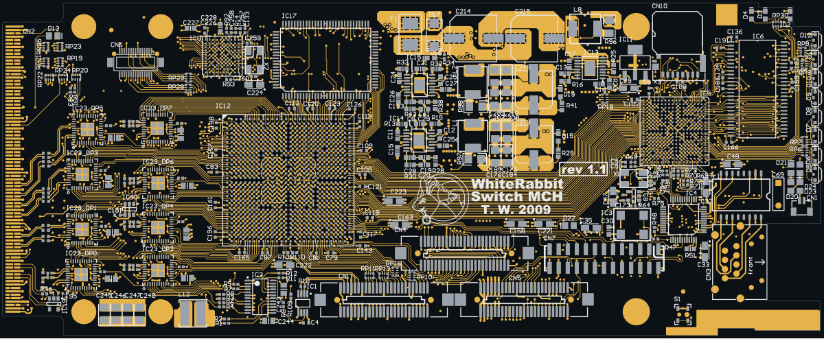
WRS V2 MCH MAIN (OHWR0017 R1) is an open-hardware circuit board from the CERN Open Hardware Repository, designed in Altium Designer: a 6-layer board of 180.6 × 73.5 mm with 630 components and 1086 nets, published under CERN-OHL-1.2.
review 84% walked · 20 findings: 1 blocker · 11 major · 8 minor (201 items)
Open in the interactive viewerRead the full review
Design review
Probe recorded 20 findings: 1 blocker · 11 major · 8 minor (201 items) on this design. Each is shown here with its reasoning; the full review links every one to the pins, nets and datasheet pages it rests on.
- NetCopperSplitblockerOpen
NetCopperSplit: 2 boards×2
e.g. “+1V2's copper is in 2 pieces: C9.2 and R104.2 are not connected to the rest of the net” · 2 different statements
At split:+1V2, split:GND
Each finding, with its own headline
split:+1V2+1V2's copper is in 2 pieces: C9.2 and R104.2 are not connected to the rest of the net
+1V2's copper is in 2 pieces: C9.2 and R104.2 are not connected to the rest of the net. Piece 1: C101.2, C103.2, C122.1, C124.1, C125.1, C127.1, C128.1, C130.1 and 92 more pin(s), on TOP_LAYER, MIDLAYER1, MIDLAYER4 and BOTTOM_LAYER, 72 drill(s), 1718.26 mm2 of pour, over (51.11, -16.3) to (136.47, 35.25). Piece 2: C9.2 and R104.2, on BOTTOM_LAYER, over (127.54, 28.06) to (131.51, 29.62). The export files every one of these pins under the net, so every connectivity check passes; the copper the fab builds leaves them apart. Usually a pour island that touches only one via of its own net, or a track ending short of its copper: join the piece to the net and export again.
split:GNDGND's copper is in 3 pieces: C70_DP0.1 and 1 other piece(s) are not connected to the rest of the net
GND's copper is in 3 pieces: C70_DP0.1 and 1 other piece(s) are not connected to the rest of the net. Piece 1: C1.2, C100.1, C101.1, C102.1, C103.1, C104.1, C105.1, C106.1 and 699 more pin(s), on TOP_LAYER, MIDLAYER1, MIDLAYER4 and BOTTOM_LAYER, 720 drill(s), 426.79 mm2 of pour, over (0, -34.78) to (177.62, 35.43). Piece 2: C70_DP0.1, on BOTTOM_LAYER, over (15.47, -21.99) to (16.12, -21.39). Piece 3: C70_DP7.1, on BOTTOM_LAYER, over (32.06, 10.45) to (32.71, 11.05). The export files every one of these pins under the net, so every connectivity check passes; the copper the fab builds leaves them apart. Usually a pour island that touches only one via of its own net, or a track ending short of its copper: join the piece to the net and export again.
TMP101 fitted on a TMP100 layout: IC39/IC40 and IC41/IC42 share I2C addresses, and IC40/IC41 ALERT outputs are tied to +3V3
The BOM orders TMP101 for IC39-IC42 but the layout is strapped for TMP100: with TMP101 fitted, IC39/IC40 and IC41/IC42 share I2C addresses and the IC40/IC41 ALERT outputs are tied to +3V3.
The BOM row IC39-IC42 has Value 'TMP101NA/250' but symbol/LibRef 'TMP100'. All four share the MCU_IO1 (SCL) / MCU_IO2 (SDA) bus.
The straps
Sensor Pin 3 Pin 5 (ADD0) As TMP100 (pin 3 = ADD1) As TMP101 (pin 3 = ALERT) IC39 GND GND unique 1001000 IC40 +3V3 GND unique 1001000, ALERT tied to +3V3 IC41 +3V3 +3V3 unique 1001010, ALERT tied to +3V3 IC42 GND +3V3 unique 1001010 Sources: TMP101 pin 3 is ALERT, an open-drain output (TMP100/TMP101 datasheet, p.3); the TMP101 has a single address pin, ADD0 (p.10).
Why it matters
- TMP101 fitted: IC39 and IC40 both answer 1001000, IC41 and IC42 both answer 1001010, and IC40/IC41 would sink +3V3 directly through ALERT when it asserts.
- TMP100 fitted: the four addresses are unique and the wiring is correct.
The BOM contradicts itself, so either the orderable value or the schematic symbol is wrong.
R34 (1 kΩ 0402, 0.0625 W) feeding power LED D16 from +12V_BULK dissipates more than its rating
R34 (1 kΩ 0402, rated 0.0625 W) feeding power LED D16 from +12V_BULK dissipates more than its rating.
D16 (green chip LED) is a rail-present indicator on +12V_BULK: R34 pin 2 on +12V_BULK, pin 1 on NetD16_1 to D16 pin 1, D16 pin 2 on GND. D16 is the only load on NetD16_1.
The numbers
Quantity Value Source R34 1 kΩ, R0402_1K_1%_0.0625W_100PPM, footprint RESC1005X40N BOM row 'R34, R82' Rating 62.5 mW BOM library name Dissipation (12 V - Vf)² / 1 kΩ derived at Vf 2.0-2.5 V 90-100 mW derived at Vf 3.5 V 72 mW derived That exceeds 62.5 mW for any visible LED, before any tolerance on the 12 V payload rail.
INA210 current monitors IC21/IC22/IC24 have 10 kΩ series input resistors: gain collapses from 200 V/V to about 18 V/V and becomes untrimmed
INA210 current monitors IC21, IC22 and IC24 have 10 kΩ series input resistors, so their gain collapses from 200 V/V to about 18 V/V and becomes untrimmed.
Each INA210 senses a 3 mΩ shunt (LR1206-R003) through 10 kΩ resistors in both inputs, with a 10 µF differential capacitor. Each output (pin 6) goes to the U1 HC4051 mux.
Monitor Rail Shunt IN+ (pin 4) IN- (pin 5) IC21 +1V2 R96 R103 10 kΩ R104 10 kΩ IC22 +2V5 R97 R105 10 kΩ R106 10 kΩ IC24 +3V3 R98 R107 10 kΩ R108 10 kΩ The numbers
Quantity Value Source Allowed series input resistance 10 Ω or less INA210 datasheet, p.14 Internal input resistance 5 kΩ, untrimmed against external parts INA210 datasheet, Table 6-1, p.15 Gain-error factor 1000 / (RS + 1000) = 1000 / 11000 = 0.091 at RS = 10 kΩ INA210 datasheet, p.15; derived Effective gain 200 × 0.091 = about 18 V/V instead of 200 V/V derived Input bias current 28 µA typical per input INA210 datasheet, p.6 Drop across each 10 kΩ 28 µA × 10 kΩ = about 0.28 V derived Why it matters
The gain is set by the ratio of the external resistors to an untrimmed internal 5 kΩ, so it varies from part to part and over temperature. Any bias-current mismatch is multiplied into the reading as offset. Firmware calibrated to 200 V/V reads the rail currents roughly 11 times low.
The published BOM mounts the schematic's '*' assembly options (R22, R58, R59, R91, D14, D18): built as listed, R21+R22 short +2V5 to GND and R59 holds the CPU JTAG TAP in reset
The published BOM mounts the schematic's '*' assembly options (R22, R58, R59, R91, D14, D18). Built as listed, R21 + R22 short +2V5 to GND and R59 holds the CPU JTAG TAP in reset.
The starred parts
The schematic uses '*' to mark the optional half of option pairs. The BOM CSV carries the same '*' but fits every one:
Part BOM value BOM fit R22, R58, R59 '0*' Mounted: Yes R91 '10k*' Mounted: Yes D14, D18 'D Schottky *' no DNP marking The BOM has no DNP/variant column, so an assembler following it fits every starred option.
What two of them do when fitted
- R21 + R22: R21 '0' to +2V5 and R22 '0*' to GND form the 'Serial boot mode select (fast/normal)' strap on the FPGA MSEL pins. Mounting both shorts +2V5 to GND.
- R59: R59 '0*' (LibRef R0402_0R_JUMPER) ties CPU_JNTRST to GND against R84 10 kOhm to +3V3. The net also joins IC5 ball U16 (NTRST) and CN7.10. Mounted, R59 holds the SAM9263 TAP in reset. The SAM9263 datasheet (p.17) says this is unnecessary: NTRST can be left unconnected, since power-on reset cells manage the JTAG reset.
For this review the six starred parts are treated as not fitted.
FPGA JTAG TMS, TCK and TDI each have both a 3.3 kΩ pull-up to +2V5 and a 3.3 kΩ pull-down to GND fitted: the lines idle at 1.25 V
The FPGA (IC12) JTAG lines TMS, TCK and TDI each have a 3.3 kΩ pull-up to +2V5 and a 3.3 kΩ pull-down to GND fitted, so they idle at 1.25 V.
The resistors
Net IC12 ball Headers Up to +2V5 Down to GND JTAG_TMS P5 CN7.16, CN5.19 R61 3k3 R78 3k3 JTAG_TCK P8 CN7.18, CN5.17 R62 3k3 R79 3k3 JTAG_TDI P7 CN7.20 R77 3k3 R81 3k3 - The BOM row 'R61, R62, R77, R78, R79, R81' is 3k3, Mounted 'Yes', quantity 6.
- Schematic sheet 'JTAG / DBGU' (PDF page 14) draws both banks with the note 'Put these resistors next to FPGA pins' and no DNP/NC marking on either.
The numbers
Quantity Value Source Idle level with no cable 2.5 V × 3.3k / (3.3k + 3.3k) = 1.25 V through 1.65 kΩ derived Why it matters
1.25 V is neither a valid high nor a valid low for 2.5 V LVCMOS. The TAP inputs float in the switching region, draw crossbar current and can see noise as TCK edges. The usual arrangement is TCK pulled down and TMS/TDI pulled up, one bank each.
- DecapOrdermajorOpen
DecapOrder: 8 findings (7 pins, 1 component)×8
Checked by the review, stands · Claude walker W2 (Cern session) — Checked: the distances are read from placement and stand as stated. Which capacitor sits nearest a supply pin at the 1-5 mm scale is a layout heuristic (Probe's starting thresholds), not a requirement of the part's datasheet on file; at this scale via and plane-spreading inductance usually dominate. Left for the owner.
At IC17, IC2.22, IC23_DP0.16, IC23_DP1.37, IC23_DP2.16, IC23_DP3.37, IC23_DP5.16, IC23_DP6.16
Each finding, with its own headline
IC17IC17 supply pins 11, 15 on '+3V3': the smallest capacitor C112 sits 4.8 mm away, behind C219 at 2.2 mm
IC17 supply pins 11, 15 on '+3V3': the smallest capacitor C112 sits 4.8 mm away, behind C219 at 2.2 mm. IC17.11: the smallest value, C112 (1 nF), is 4.8 mm from the pin and C219 (100 nF) 2.2 mm: the high-frequency part sits behind more inductance than the bulk part, which needs it least. IC17.15: the smallest value, C120 (10 nF), is 3.8 mm from the pin and C217 (100 nF) 2.0 mm: the high-frequency part sits behind more inductance than the bulk part, which needs it least. Swap them, or bring the smallest value to the pin: it serves the fastest current and is the one the loop inductance defeats. Distances are pad centre to pin centre in the board plane. The 5 mm radius, the 10x value step and the 1 mm / 1.5x tie tolerance are Probe's starting values.
IC2.22IC2 supply pin 22 on '+3V3': the smallest capacitor C5 sits 4.7 mm away, behind C6 at 2.2 mm
IC2 supply pin 22 on '+3V3': the smallest capacitor C5 sits 4.7 mm away, behind C6 at 2.2 mm. IC2.22: the smallest value, C5 (1 nF), is 4.7 mm from the pin and C6 (100 nF) 2.2 mm: the high-frequency part sits behind more inductance than the bulk part, which needs it least. Swap them, or bring the smallest value to the pin: it serves the fastest current and is the one the loop inductance defeats. Distances are pad centre to pin centre in the board plane. The 5 mm radius, the 10x value step and the 1 mm / 1.5x tie tolerance are Probe's starting values.
IC23_DP0.16IC23_DP0 supply pin 16 on '+2V5_PHY': the smallest capacitor C250_DP0 sits 1.8 mm away, behind C74_DP0 at 0.4 mm
IC23_DP0 supply pin 16 on '+2V5_PHY': the smallest capacitor C250_DP0 sits 1.8 mm away, behind C74_DP0 at 0.4 mm. IC23_DP0.16: the smallest value, C250_DP0 (10 nF), is 1.8 mm from the pin and C74_DP0 (100 nF) 0.4 mm: the high-frequency part sits behind more inductance than the bulk part, which needs it least. Swap them, or bring the smallest value to the pin: it serves the fastest current and is the one the loop inductance defeats. Distances are pad centre to pin centre in the board plane. The 5 mm radius, the 10x value step and the 1 mm / 1.5x tie tolerance are Probe's starting values.
IC23_DP1.37IC23_DP1 supply pin 37 on '+2V5_PHY': the smallest capacitor C70_DP1 sits 4.3 mm away, behind C251_DP1 at 2.6 mm
IC23_DP1 supply pin 37 on '+2V5_PHY': the smallest capacitor C70_DP1 sits 4.3 mm away, behind C251_DP1 at 2.6 mm. IC23_DP1.37: the smallest value, C70_DP1 (10 nF), is 4.3 mm from the pin and C251_DP1 (100 nF) 2.6 mm: the high-frequency part sits behind more inductance than the bulk part, which needs it least. Swap them, or bring the smallest value to the pin: it serves the fastest current and is the one the loop inductance defeats. Distances are pad centre to pin centre in the board plane. The 5 mm radius, the 10x value step and the 1 mm / 1.5x tie tolerance are Probe's starting values.
IC23_DP2.16IC23_DP2 supply pin 16 on '+2V5_PHY': the smallest capacitor C250_DP2 sits 1.7 mm away, behind C74_DP2 at 0.2 mm
IC23_DP2 supply pin 16 on '+2V5_PHY': the smallest capacitor C250_DP2 sits 1.7 mm away, behind C74_DP2 at 0.2 mm. IC23_DP2.16: the smallest value, C250_DP2 (10 nF), is 1.7 mm from the pin and C74_DP2 (100 nF) 0.2 mm: the high-frequency part sits behind more inductance than the bulk part, which needs it least. Swap them, or bring the smallest value to the pin: it serves the fastest current and is the one the loop inductance defeats. Distances are pad centre to pin centre in the board plane. The 5 mm radius, the 10x value step and the 1 mm / 1.5x tie tolerance are Probe's starting values.
IC23_DP3.37IC23_DP3 supply pin 37 on '+2V5_PHY': the smallest capacitor C70_DP3 sits 4.3 mm away, behind C251_DP3 at 2.6 mm
IC23_DP3 supply pin 37 on '+2V5_PHY': the smallest capacitor C70_DP3 sits 4.3 mm away, behind C251_DP3 at 2.6 mm. IC23_DP3.37: the smallest value, C70_DP3 (10 nF), is 4.3 mm from the pin and C251_DP3 (100 nF) 2.6 mm: the high-frequency part sits behind more inductance than the bulk part, which needs it least. Swap them, or bring the smallest value to the pin: it serves the fastest current and is the one the loop inductance defeats. Distances are pad centre to pin centre in the board plane. The 5 mm radius, the 10x value step and the 1 mm / 1.5x tie tolerance are Probe's starting values.
IC23_DP5.16IC23_DP5 supply pin 16 on '+2V5_PHY': the smallest capacitor C250_DP5 sits 3.6 mm away, behind C251_DP5 at 0.9 mm
IC23_DP5 supply pin 16 on '+2V5_PHY': the smallest capacitor C250_DP5 sits 3.6 mm away, behind C251_DP5 at 0.9 mm. IC23_DP5.16: the smallest value, C250_DP5 (10 nF), is 3.6 mm from the pin and C251_DP5 (100 nF) 0.9 mm: the high-frequency part sits behind more inductance than the bulk part, which needs it least. Swap them, or bring the smallest value to the pin: it serves the fastest current and is the one the loop inductance defeats. Distances are pad centre to pin centre in the board plane. The 5 mm radius, the 10x value step and the 1 mm / 1.5x tie tolerance are Probe's starting values.
IC23_DP6.16IC23_DP6 supply pin 16 on '+2V5_PHY': the smallest capacitor C250_DP6 sits 1.8 mm away, behind C74_DP6 at 0.4 mm
IC23_DP6 supply pin 16 on '+2V5_PHY': the smallest capacitor C250_DP6 sits 1.8 mm away, behind C74_DP6 at 0.4 mm. IC23_DP6.16: the smallest value, C250_DP6 (10 nF), is 1.8 mm from the pin and C74_DP6 (100 nF) 0.4 mm: the high-frequency part sits behind more inductance than the bulk part, which needs it least. Swap them, or bring the smallest value to the pin: it serves the fastest current and is the one the loop inductance defeats. Distances are pad centre to pin centre in the board plane. The 5 mm radius, the 10x value step and the 1 mm / 1.5x tie tolerance are Probe's starting values.
- DecapViaFanoutmajorOpen
DecapViaFanout: 4 components×4
Checked by the review, stands · Claude walker W2 (Cern session) — Checked: the fanout length is read from the copper and stands; 0.5 nH is Probe's starting value, not a datasheet requirement. Whether it matters depends on the rail's PDN target, which is not stated. Left for the owner.
At C130, C134, C149, C181
Each finding, with its own headline
C130C130 on '+1V2': its rail pad reaches its via over 2.65 mm of track, adding about 0.74 nH to its loop, past Probe's 0.5 nH starting value; put the vias at the pads
C130 on '+1V2': its rail pad reaches its via over 2.65 mm of track, adding about 0.74 nH to its loop, past Probe's 0.5 nH starting value; put the vias at the pads. C130.1 (rail) runs 2.65 mm along its copper to its nearest via, 1.65 mm past the 1 mm beside the pad: 0.74 nH; C130.2 (ground) not measured: the pad sits in a pour of its net on its own layer, which has no track length to measure. Each run past the pad as one conductor of a pair 1.20 mm apart (the pad pitch), 0.2 l ln(D/R) nH with R 0.127 mm (the track's width is not read): 0.74 nH in all. Put the vias at the pads (or in them), one per pad at least, the rail's and the ground's close together; the capacitor's own inductance as mounted is 1.18 nH (pad 0.07 nH + no via of the first net within 1 mm of its pad: the study's 0.6 nH per mm of 1.35 mm depth, ASSUMED). 0.5 nH is Probe's starting value, about the whole mounted inductance of a well-mounted 0402.
C134C134 on '+3V3': its rail pad reaches its via over 1.65 mm of track and its ground pad over 6.00 mm, adding about 2.54 nH to its loop, past Probe's 0.5 nH starting value; put the vias at the pads
C134 on '+3V3': its rail pad reaches its via over 1.65 mm of track and its ground pad over 6.00 mm, adding about 2.54 nH to its loop, past Probe's 0.5 nH starting value; put the vias at the pads. C134.1 (rail) runs 1.65 mm along its copper to its nearest via, 0.65 mm past the 1 mm beside the pad: 0.29 nH; C134.2 (ground) runs at least 6.00 mm along its copper to its nearest via, 5.00 mm past the 1 mm beside the pad: 2.25 nH. Each run past the pad as one conductor of a pair 1.20 mm apart (the pad pitch), 0.2 l ln(D/R) nH with R 0.127 mm (the track's width is not read): 2.54 nH in all. Put the vias at the pads (or in them), one per pad at least, the rail's and the ground's close together; the capacitor's own inductance as mounted is 1.18 nH (pad 0.07 nH + no via of the first net within 1 mm of its pad: the study's 0.6 nH per mm of 1.35 mm depth, ASSUMED). 0.5 nH is Probe's starting value, about the whole mounted inductance of a well-mounted 0402.
C149C149 on '+3V3': its rail pad reaches its via over 1.38 mm of track and its ground pad over 3.16 mm, adding about 1.14 nH to its loop, past Probe's 0.5 nH starting value; put the vias at the pads
C149 on '+3V3': its rail pad reaches its via over 1.38 mm of track and its ground pad over 3.16 mm, adding about 1.14 nH to its loop, past Probe's 0.5 nH starting value; put the vias at the pads. C149.2 (rail) runs 1.38 mm along its copper to its nearest via, 0.38 mm past the 1 mm beside the pad: 0.17 nH; C149.1 (ground) runs 3.16 mm along its copper to its nearest via, 2.16 mm past the 1 mm beside the pad: 0.97 nH. Each run past the pad as one conductor of a pair 1.20 mm apart (the pad pitch), 0.2 l ln(D/R) nH with R 0.127 mm (the track's width is not read): 1.14 nH in all. Put the vias at the pads (or in them), one per pad at least, the rail's and the ground's close together; the capacitor's own inductance as mounted is 0.53 nH (pad 0.07 nH + no via of the first net within 1 mm of its pad: the study's 0.6 nH per mm of 0.27 mm depth, ASSUMED). 0.5 nH is Probe's starting value, about the whole mounted inductance of a well-mounted 0402.
C181C181 on '+3V3': its ground pad over 5.14 mm, adding about 1.86 nH to its loop, past Probe's 0.5 nH starting value; put the vias at the pads
C181 on '+3V3': its ground pad over 5.14 mm, adding about 1.86 nH to its loop, past Probe's 0.5 nH starting value; put the vias at the pads. C181.2 (rail) not measured: its own track joins it to IC6.14 (1.76 mm) before any via: it serves that pin directly, and its loop does not run through its vias; C181.1 (ground) runs 5.14 mm along its copper to its nearest via, 4.14 mm past the 1 mm beside the pad: 1.86 nH. Each run past the pad as one conductor of a pair 1.20 mm apart (the pad pitch), 0.2 l ln(D/R) nH with R 0.127 mm (the track's width is not read): 1.86 nH in all. Put the vias at the pads (or in them), one per pad at least, the rail's and the ground's close together; the capacitor's own inductance as mounted is 1.18 nH (pad 0.07 nH + no via of the first net within 1 mm of its pad: the study's 0.6 nH per mm of 1.35 mm depth, ASSUMED). 0.5 nH is Probe's starting value, about the whole mounted inductance of a well-mounted 0402.
- FiducialMissingmajorOpen
FiducialMissing: 2 boards×2
Checked by the review, stands · Claude walker (cern session) — No fiducial on this board: none of the 630 BOM rows is a FID*/FTG*/fiducial part and the rule found no fiducial-attribute pad. Not refuted; whether a production panel carries them is for the owner.
At bottom, top
Each finding, with its own headline
bottomThe bottom side carries 246 SMT component(s) and no fiducial was found on it
The bottom side carries 246 SMT component(s) but no fiducial was found on it — a placement machine has no optical reference to align to. Probe found no pad labelled .pad_usage=g_fiducial/l_fiducial (basis pad_usage); no single-pad, netless, undrilled component whose 0.5-3 mm round pad has a concentric solder-mask opening at least 1.5x its diameter with no other copper inside it (basis geometry); and no component whose refdes starts FID or whose part or package name contains FIDUCIAL (basis footprint-name). If your library names fiducials something Probe does not recognise, mark this benign — disposition_finding(rule='FiducialMissing', entity='bottom', status='benign', reason=…) — the name match only ever silences this check, it never asserts anything. If the side really has no fiducial, say so with status='confirmed': that answers the finding and keeps it gating release.
topThe top side carries 221 SMT component(s) and no fiducial was found on it
The top side carries 221 SMT component(s) but no fiducial was found on it — a placement machine has no optical reference to align to. Probe found no pad labelled .pad_usage=g_fiducial/l_fiducial (basis pad_usage); no single-pad, netless, undrilled component whose 0.5-3 mm round pad has a concentric solder-mask opening at least 1.5x its diameter with no other copper inside it (basis geometry); and no component whose refdes starts FID or whose part or package name contains FIDUCIAL (basis footprint-name). If your library names fiducials something Probe does not recognise, mark this benign — disposition_finding(rule='FiducialMissing', entity='top', status='benign', reason=…) — the name match only ever silences this check, it never asserts anything. If the side really has no fiducial, say so with status='confirmed': that answers the finding and keeps it gating release.
- PartLifecyclemajorOpen
PartLifecycle: 4 part numbers×4
4 Obsolete · on 4 placements
At IC11, IC18, IC9, U1
Each finding, with its own headline
IC11FAN1112SX on IC11: the distributor catalogue reports "Obsolete" for onsemi's FAN1112SX
FAN1112SX on IC11: the distributor catalogue reports "Obsolete" for onsemi's FAN1112SX — a sourcing/longevity risk to confirm against the MANUFACTURER before acting. This board's BOM names no manufacturer for it, so whether that is the fitted maker's product was not checked. A distributor delisting is not the same claim as the part being unavailable; check the vendor's own lifecycle/product-change notice for the status and any named successor. Re-read the source: GET /api/odb/parts/FAN1112SX/providers (which provider said it, the maker and part number it matched, its own words, and when we asked). No approved alternate is recorded for this position.
IC18DS18B20 on IC18: the distributor catalogue reports "Obsolete" for Analog Devices Inc./Maxim Integrated's DS18B20
DS18B20 on IC18: the distributor catalogue reports "Obsolete" for Analog Devices Inc./Maxim Integrated's DS18B20 — a sourcing/longevity risk to confirm against the MANUFACTURER before acting. This board's BOM names no manufacturer for it, so whether that is the fitted maker's product was not checked. A distributor delisting is not the same claim as the part being unavailable; check the vendor's own lifecycle/product-change notice for the status and any named successor. Re-read the source: GET /api/odb/parts/DS18B20/providers (which provider said it, the maker and part number it matched, its own words, and when we asked). THE LAST BUY DATE HAS PASSED (2011-03-08, 5,731 day(s) ago), so this is a substitution rather than a buy. The distributor reports NONE left. No approved alternate is recorded for this position.
IC9AT91SAM7X256-CU on IC9: the distributor catalogue reports "Obsolete" for Microchip Technology's AT91SAM7X256-CU
AT91SAM7X256-CU on IC9: the distributor catalogue reports "Obsolete" for Microchip Technology's AT91SAM7X256-CU — a sourcing/longevity risk to confirm against the MANUFACTURER before acting. This board's BOM names no manufacturer for it, so whether that is the fitted maker's product was not checked. A distributor delisting is not the same claim as the part being unavailable; check the vendor's own lifecycle/product-change notice for the status and any named successor. Re-read the source: GET /api/odb/parts/AT91SAM7X256-CU/providers (which provider said it, the maker and part number it matched, its own words, and when we asked). No approved alternate is recorded for this position.
U1MC74HC4051ADTR2 on U1: the distributor catalogue reports "Obsolete" for onsemi's MC74HC4051ADTR2
MC74HC4051ADTR2 on U1: the distributor catalogue reports "Obsolete" for onsemi's MC74HC4051ADTR2 — a sourcing/longevity risk to confirm against the MANUFACTURER before acting. This board's BOM names no manufacturer for it, so whether that is the fitted maker's product was not checked. A distributor delisting is not the same claim as the part being unavailable; check the vendor's own lifecycle/product-change notice for the status and any named successor. Re-read the source: GET /api/odb/parts/MC74HC4051ADTR2/providers (which provider said it, the maker and part number it matched, its own words, and when we asked). THE LAST BUY DATE HAS PASSED (2011-07-23, 5,594 day(s) ago), so this is a substitution rather than a buy. The distributor reports NONE left. No approved alternate is recorded for this position.
- ReferencePlaneDiscontinuitymajorOpen
ReferencePlaneDiscontinuity: 89 boards×89
Checked by the review, stands · Claude walker W2 (Cern session) — Checked: the crossings and reference changes are read from the copper and stand as stated. No edge-rate or impedance requirement on file makes them a defect: most nets involved are slow control/IO, and the stackup's stated planes give a nearby return for most crossings as reported. Layout practice, left for the owner.
At along@MIDLAYER4:+12V_BACKPLANE|+1V2, along@MIDLAYER4:+12V_BULK|+1V2, gap:GND:hole 151.99,-2.04|156.82,-1.78, gap:GND:hole 151.99,-8.31|152.25,-1.78, gap:POWER:hole 100.79,25.91|101.04,32.61, gap:POWER:hole 107.56,-31.65|107.82,-23.47 and 83 more
Each finding, with its own headline
along@MIDLAYER4:+12V_BACKPLANE|+1V213 nets run ALONG the split between the +12V_BACKPLANE and +1V2 planes on MIDLAYER4 at 13 places, the longest 27.83 mm; the impedance rises from 65 ohm to 72 ohm there at worst, 5.1 % of each edge reflected (fastest: PC11 at 100 ps 10-90 %, ASSUMED)
On MIDLAYER4 the +12V_BACKPLANE and +1V2 planes part, and 13 nets run down the slot between them at 13 place(s), rather than across it. This is not a crossing: the return still follows the track, in the plane on its other side and in the slot's edges, so it does not detour. What changes is the track's own impedance. With the plane gone from under it on this side for that length, its field reaches further, to the slot's edges and to the next plane beyond, so its capacitance falls and its impedance rises; every edge travelling down it is partly reflected where it enters the stretch and again where it leaves, by (Z2 - Z1)/(Z2 + Z1). The longer the stretch against the edge's rise, the more of the edge sees the full step. A crossing is generally the worse fault; a mismatch is not free. Over solid plane each track is 65 ohm; along the slot 67 ohm to 72 ohm, reflecting up to 5.1 % of each edge (a method-of-moments field solve of the cross-section, one dielectric; were the slot's edges to carry none of the return, up to 72 ohm). At 6 of the 13 place(s) the rise is within 10 %, the tolerance controlled impedance is commonly built to (the stackup states none); the rest exceed it or cannot be said, so the finding is a warning. One decision covers the split line's slot: whether these tracks may run down it, or should be moved over solid plane.
- 'WD_NRST' on MIDLAYER1 at (83, 9.45), 16.24 mm, running ALONG the split for 8.04 mm, not across it, 65 ohm over solid plane, 72 ohm along it: 5.1 % of each edge reflected; other side: (negative-layer field) on POWER, 0.27 mm from the track against 0.27 mm to MIDLAYER4: 50% of the return on MIDLAYER4
- 'DRXD' on MIDLAYER1 at (83.25, 9.63), 15.94 mm, running ALONG the split for 7.58 mm, not across it, 65 ohm over solid plane, 72 ohm along it: 5.1 % of each edge reflected; other side: (negative-layer field) on POWER, 0.27 mm from the track against 0.27 mm to MIDLAYER4: 50% of the return on MIDLAYER4
- 'UTCA_PWRON#' on MIDLAYER1 at (83.51, 9.8), 15.64 mm, running ALONG the split for 7.71 mm, not across it, 65 ohm over solid plane, 72 ohm along it: 5.1 % of each edge reflected; other side: (negative-layer field) on POWER, 0.27 mm from the track against 0.27 mm to MIDLAYER4: 50% of the return on MIDLAYER4
- 'DTXD' on MIDLAYER1 at (83.76, 9.98), 15.35 mm, running ALONG the split for 7.95 mm, not across it, 65 ohm over solid plane, 72 ohm along it: 5.1 % of each edge reflected; other side: (negative-layer field) on POWER, 0.27 mm from the track against 0.27 mm to MIDLAYER4: 50% of the return on MIDLAYER4
- 'WD_JTAG_TDI' on MIDLAYER1 at (84.02, 10.16), 15.05 mm, running ALONG the split for 8.04 mm, not across it, 65 ohm over solid plane, 72 ohm along it: 5.1 % of each edge reflected; other side: (negative-layer field) on POWER, 0.27 mm from the track against 0.27 mm to MIDLAYER4: 50% of the return on MIDLAYER4
- 'WD_JTAG_TMS' on MIDLAYER1 at (84.28, 10.34), 14.75 mm, running ALONG the split for 8.04 mm, not across it, 65 ohm over solid plane, 72 ohm along it: 5 % of each edge reflected; other side: (negative-layer field) on POWER, 0.27 mm from the track against 0.27 mm to MIDLAYER4: 50% of the return on MIDLAYER4
- 'GPIO2' on MIDLAYER1 at (104.07, 33.27), 31.7 mm, running ALONG the split for 27.57 mm, not across it, 65 ohm over solid plane, 72 ohm along it: 4.9 % of each edge reflected; other side: (negative-layer field) on POWER, 0.27 mm from the track against 0.27 mm to MIDLAYER4: 50% of the return on MIDLAYER4
- 'PC15' on MIDLAYER1 at (104.17, 33.53), 31.71 mm, running ALONG the split for 27.71 mm, not across it, 65 ohm over solid plane, 71 ohm along it: 4.4 % of each edge reflected; other side: (negative-layer field) on POWER, 0.27 mm from the track against 0.27 mm to MIDLAYER4: 50% of the return on MIDLAYER4
- 'GPIO3' on MIDLAYER1 at (104.02, 33.02), 31.74 mm, running ALONG the split for 27.53 mm, not across it, 65 ohm over solid plane, 71 ohm along it: 4.3 % of each edge reflected; other side: (negative-layer field) on POWER, 0.27 mm from the track against 0.27 mm to MIDLAYER4: 50% of the return on MIDLAYER4
- 'WD_JTAG_TDO' on MIDLAYER1 at (84.53, 10.52), 14.45 mm, running ALONG the split for 7.85 mm, not across it, 65 ohm over solid plane, 71 ohm along it: 4.2 % of each edge reflected; other side: (negative-layer field) on POWER, 0.27 mm from the track against 0.27 mm to MIDLAYER4: 50% of the return on MIDLAYER4
- 'PC11' on MIDLAYER1 at (104.27, 33.83), 31.76 mm, running ALONG the split for 27.83 mm, not across it, 65 ohm over solid plane, 68 ohm along it: 2.1 % of each edge reflected; other side: (negative-layer field) on POWER, 0.27 mm from the track against 0.27 mm to MIDLAYER4: 50% of the return on MIDLAYER4
- 'GPIO7' on MIDLAYER1 at (103.96, 32.76), 31.78 mm, running ALONG the split for 27.34 mm, not across it, 65 ohm over solid plane, 68 ohm along it: 1.9 % of each edge reflected; other side: (negative-layer field) on POWER, 0.27 mm from the track against 0.27 mm to MIDLAYER4: 50% of the return on MIDLAYER4
- and 1 more
Every site is a row of this finding's evidence, keyed by net, layers and position. GET /api/odb/boards/20/reference-planes?group=along%40MIDLAYER4%3A%2B12V_BACKPLANE%7C%2B1V2 serves each with its own layer_image region; all of them lie in x 77.64..119.74, y 3.09..34.83 mm (board frame, Y up).
Read from the copper as drawn on the reference layer, along each track's centreline at exact breakpoints. The reference is the copper beside the track, never the layer's type or name. Whether it matters depends on each signal's edge rate, which nothing on file states for these nets: a slow static line crosses a split harmlessly, a fast edge does not.
along@MIDLAYER4:+12V_BULK|+1V26 nets run ALONG the split between the +12V_BULK and +1V2 planes on MIDLAYER4 at 6 places, the longest 15.41 mm; the impedance rises from 65 ohm to 72 ohm there at worst, 5.1 % of each edge reflected (fastest: MAIN_FPGA_DIN at 100 ps 10-90 %, ASSUMED)
On MIDLAYER4 the +12V_BULK and +1V2 planes part, and 6 nets run down the slot between them at 6 place(s), rather than across it. This is not a crossing: the return still follows the track, in the plane on its other side and in the slot's edges, so it does not detour. What changes is the track's own impedance. With the plane gone from under it on this side for that length, its field reaches further, to the slot's edges and to the next plane beyond, so its capacitance falls and its impedance rises; every edge travelling down it is partly reflected where it enters the stretch and again where it leaves, by (Z2 - Z1)/(Z2 + Z1). The longer the stretch against the edge's rise, the more of the edge sees the full step. A crossing is generally the worse fault; a mismatch is not free. Over solid plane each track is 65 ohm; along the slot 66 ohm to 72 ohm, reflecting up to 5.1 % of each edge (a method-of-moments field solve of the cross-section, one dielectric; were the slot's edges to carry none of the return, up to 72 ohm). At 5 of the 6 place(s) the rise is within 10 %, the tolerance controlled impedance is commonly built to (the stackup states none); the rest exceed it or cannot be said, so the finding is a warning. One decision covers the split line's slot: whether these tracks may run down it, or should be moved over solid plane.
- 'PB31' on MIDLAYER1 at (84.53, -22.32), 54.3 mm, running ALONG the split for 11.29 mm, not across it, 65 ohm over solid plane, 72 ohm along it: 5.1 % of each edge reflected; other side: +2V5 on POWER, 0.27 mm from the track against 0.27 mm to MIDLAYER4: 50% of the return on MIDLAYER4
- 'JTAG_TDI' on MIDLAYER1 at (85.76, -32.43), 60.07 mm, running ALONG the split for 8.73 mm, not across it, 65 ohm over solid plane, 70 ohm along it: 3.5 % of each edge reflected; other side: (negative-layer field) on POWER, 0.27 mm from the track against 0.27 mm to MIDLAYER4: 50% of the return on MIDLAYER4
- 'MAIN_FPGA_DIN' on MIDLAYER1 at (84.3, -22.65), 56.18 mm, running ALONG the split for 14.47 mm, not across it, 65 ohm over solid plane, 68 ohm along it: 2.4 % of each edge reflected; other side: +2V5 on POWER, 0.27 mm from the track against 0.27 mm to MIDLAYER4: 50% of the return on MIDLAYER4
- 'JTAG_TMS' on MIDLAYER1 at (82.07, -30.95), 60.96 mm, running ALONG the split for 14.57 mm, not across it, 65 ohm over solid plane, 68 ohm along it: 1.9 % of each edge reflected; other side: +2V5 on POWER, 0.27 mm from the track against 0.27 mm to MIDLAYER4: 50% of the return on MIDLAYER4
- 'NetIC12_P4' on MIDLAYER1 at (82.05, -31.31), 61.04 mm, running ALONG the split for 13.85 mm, not across it, 65 ohm over solid plane, 66 ohm along it: 0.3 % of each edge reflected; other side: +2V5 on POWER, 0.27 mm from the track against 0.27 mm to MIDLAYER4: 50% of the return on MIDLAYER4
- 'JTAG_TCK' on MIDLAYER1 at (82.03, -30.62), 60.17 mm, running ALONG the split for 15.41 mm, not across it, 65 ohm over solid plane, 66 ohm along it: 0.3 % of each edge reflected; other side: +2V5 on POWER, 0.27 mm from the track against 0.27 mm to MIDLAYER4: 50% of the return on MIDLAYER4
Every site is a row of this finding's evidence, keyed by net, layers and position. GET /api/odb/boards/20/reference-planes?group=along%40MIDLAYER4%3A%2B12V_BULK%7C%2B1V2 serves each with its own layer_image region; all of them lie in x 58.53..104.23, y -33.43..-6.35 mm (board frame, Y up).
Read from the copper as drawn on the reference layer, along each track's centreline at exact breakpoints. The reference is the copper beside the track, never the layer's type or name. Whether it matters depends on each signal's edge rate, which nothing on file states for these nets: a slow static line crosses a split harmlessly, a fast edge does not.
gap:GND:hole 151.99,-2.04|156.82,-1.78'PB31' crosses one gap in GND's negative-plane field at 1 place, the longest 0.25 mm (fastest: PB31 at 100 ps 10-90 %, ASSUMED)
Along 'PB31' on BOTTOM_LAYER, GND is a negative layer (copper everywhere inside the profile), and its field is cleared for 0.25 mm under the track at (152.38, -1.91). The layer does not state the nets either side, so whether this is a split between two planes or a void in one is not said; either way the return current has to go round it. What cleared it: the hole at x 151.99..156.82, y -2.04..-1.78. One decision covers the void: whether these tracks may cross it, or the plane should be filled under them. No crossing has a plane on the track's other side, so the whole return meets the break.
- 'PB31' on BOTTOM_LAYER at (152.38, -1.91), 0.25 mm; other side: none: the signal layer is outermost
Every site is a row of this finding's evidence, keyed by net, layers and position. GET /api/odb/boards/20/reference-planes?group=gap%3AGND%3Ahole%20151.99%2C-2.04%7C156.82%2C-1.78 serves each with its own layer_image region; all of them lie in x 151.38..153.38, y -3.04..-0.78 mm (board frame, Y up).
Read from the copper as drawn on the reference layer, along each track's centreline at exact breakpoints. The reference is the copper beside the track, never the layer's type or name. Whether it matters depends on each signal's edge rate, which nothing on file states for these nets: a slow static line crosses a split harmlessly, a fast edge does not.
gap:GND:hole 151.99,-8.31|152.25,-1.782 nets cross one gap in GND's negative-plane field at 2 places, the longest 0.36 mm (fastest: NetIC4_13 at 100 ps 10-90 %, ASSUMED)
Along 'NetIC4_13' on BOTTOM_LAYER, GND is a negative layer (copper everywhere inside the profile), and its field is cleared for 0.36 mm under the track at (152.12, -6.76). The layer does not state the nets either side, so whether this is a split between two planes or a void in one is not said; either way the return current has to go round it. 2 places on 2 net(s) cross it, listed below, the longest first. What cleared it: the hole at x 151.99..152.25, y -8.31..-1.78. One decision covers the void: whether these tracks may cross it, or the plane should be filled under them. No crossing has a plane on the track's other side, so the whole return meets the break.
- 'NetIC4_13' on BOTTOM_LAYER at (152.12, -6.76), 0.36 mm; other side: none: the signal layer is outermost
- 'PB31' on BOTTOM_LAYER at (152.12, -3.51), 0.36 mm; other side: none: the signal layer is outermost
Every site is a row of this finding's evidence, keyed by net, layers and position. GET /api/odb/boards/20/reference-planes?group=gap%3AGND%3Ahole%20151.99%2C-8.31%7C152.25%2C-1.78 serves each with its own layer_image region; all of them lie in x 150.99..153.25, y -7.89..-2.38 mm (board frame, Y up).
Read from the copper as drawn on the reference layer, along each track's centreline at exact breakpoints. The reference is the copper beside the track, never the layer's type or name. Whether it matters depends on each signal's edge rate, which nothing on file states for these nets: a slow static line crosses a split harmlessly, a fast edge does not.
gap:POWER:hole 100.79,25.91|101.04,32.6115 nets cross one gap in POWER's negative-plane field at 15 places, the longest 0.36 mm (fastest: AD4 at 100 ps 10-90 %, ASSUMED)
Along 'MCU_IO40' on MIDLAYER1, POWER is a negative layer (copper everywhere inside the profile), and its field is cleared for 0.36 mm under the track at (100.91, 26.26). The layer does not state the nets either side, so whether this is a split between two planes or a void in one is not said; either way the return current has to go round it. 15 places on 15 net(s) cross it, listed below, the longest first. What cleared it: the hole at x 100.79..101.04, y 25.91..32.61. One decision covers the void: whether these tracks may cross it, or the plane should be filled under them. 11 of the 15 crossing(s) have a plane on the track's other side at most twice as far away as the broken one (to first order each plane beside a stripline carries a share of the return inversely proportional to its distance from the track). The rest leave most or all of the return to the break, so the finding is a warning.
- 'GPIO6' on MIDLAYER1 at (100.91, 32.51), 0.33 mm; other side: no plane on MIDLAYER4
- 'GPIO1' on MIDLAYER1 at (100.91, 31.75), 0.25 mm; other side: no plane on MIDLAYER4
- 'GPIO4' on MIDLAYER1 at (100.91, 32), 0.25 mm; other side: no plane on MIDLAYER4
- 'GPIO5' on MIDLAYER1 at (100.91, 32.26), 0.25 mm; other side: no plane on MIDLAYER4
- 'MCU_IO40' on MIDLAYER1 at (100.91, 26.26), 0.36 mm; other side: +12V_BULK on MIDLAYER4, 0.27 mm from the track against 0.27 mm to POWER: 50% of the return on POWER
- 'SCK' on MIDLAYER1 at (100.86, 26.79), 0.31 mm; other side: +12V_BULK on MIDLAYER4, 0.27 mm from the track against 0.27 mm to POWER: 50% of the return on POWER
- 'AD4' on MIDLAYER1 at (100.91, 29.12), 0.25 mm; other side: +12V_BULK on MIDLAYER4, 0.27 mm from the track against 0.27 mm to POWER: 50% of the return on POWER
- 'GPIO0' on MIDLAYER1 at (100.91, 31.49), 0.25 mm; other side: +12V_BULK on MIDLAYER4, 0.27 mm from the track against 0.27 mm to POWER: 50% of the return on POWER
- 'MCU_IO1' on MIDLAYER1 at (100.91, 28.87), 0.25 mm; other side: +12V_BULK on MIDLAYER4, 0.27 mm from the track against 0.27 mm to POWER: 50% of the return on POWER
- 'MCU_IO2' on MIDLAYER1 at (100.91, 28.61), 0.25 mm; other side: +12V_BULK on MIDLAYER4, 0.27 mm from the track against 0.27 mm to POWER: 50% of the return on POWER
- 'MCU_IO39' on MIDLAYER1 at (100.91, 28.1), 0.25 mm; other side: +12V_BULK on MIDLAYER4, 0.27 mm from the track against 0.27 mm to POWER: 50% of the return on POWER
- 'MCU_IO41' on MIDLAYER1 at (100.91, 27.47), 0.25 mm; other side: +12V_BULK on MIDLAYER4, 0.27 mm from the track against 0.27 mm to POWER: 50% of the return on POWER
- and 3 more
Every site is a row of this finding's evidence, keyed by net, layers and position. GET /api/odb/boards/20/reference-planes?group=gap%3APOWER%3Ahole%20100.79%2C25.91%7C101.04%2C32.61 serves each with its own layer_image region; all of them lie in x 99.71..102.04, y 25.14..33.51 mm (board frame, Y up).
Read from the copper as drawn on the reference layer, along each track's centreline at exact breakpoints. The reference is the copper beside the track, never the layer's type or name. Whether it matters depends on each signal's edge rate, which nothing on file states for these nets: a slow static line crosses a split harmlessly, a fast edge does not.
gap:POWER:hole 107.56,-31.65|107.82,-23.474 nets cross one gap in POWER's negative-plane field at 4 places, the longest 0.25 mm (fastest: MAIN_FPGA_DIN at 100 ps 10-90 %, ASSUMED)
Along 'JTAG_TCK' on MIDLAYER1, POWER is a negative layer (copper everywhere inside the profile), and its field is cleared for 0.25 mm under the track at (107.69, -31). The layer does not state the nets either side, so whether this is a split between two planes or a void in one is not said; either way the return current has to go round it. 4 places on 4 net(s) cross it, listed below, the longest first. What cleared it: the hole at x 107.56..107.82, y -31.65..-23.47. One decision covers the void: whether these tracks may cross it, or the plane should be filled under them. No crossing has a plane on the track's other side, so the whole return meets the break.
- 'JTAG_TCK' on MIDLAYER1 at (107.69, -31), 0.25 mm; other side: no plane on MIDLAYER4
- 'JTAG_TMS' on MIDLAYER1 at (107.69, -31.36), 0.25 mm; other side: no plane on MIDLAYER4
- 'MAIN_FPGA_DIN' on MIDLAYER1 at (107.69, -30.65), 0.25 mm; other side: no plane on MIDLAYER4
- 'PB31' on MIDLAYER1 at (107.69, -30.33), 0.25 mm; other side: no plane on MIDLAYER4
Every site is a row of this finding's evidence, keyed by net, layers and position. GET /api/odb/boards/20/reference-planes?group=gap%3APOWER%3Ahole%20107.56%2C-31.65%7C107.82%2C-23.47 serves each with its own layer_image region; all of them lie in x 106.56..108.82, y -32.36..-29.33 mm (board frame, Y up).
Read from the copper as drawn on the reference layer, along each track's centreline at exact breakpoints. The reference is the copper beside the track, never the layer's type or name. Whether it matters depends on each signal's edge rate, which nothing on file states for these nets: a slow static line crosses a split harmlessly, a fast edge does not.
gap:POWER:hole 107.56,-32.2|108.37,-31.39'NetIC12_P4' crosses one gap in POWER's negative-plane field at 1 place, the longest 0.36 mm (fastest: NetIC12_P4 at 100 ps 10-90 %, ASSUMED)
Along 'NetIC12_P4' on MIDLAYER1, POWER is a negative layer (copper everywhere inside the profile), and its field is cleared for 0.36 mm under the track at (107.89, -31.72). The layer does not state the nets either side, so whether this is a split between two planes or a void in one is not said; either way the return current has to go round it. What cleared it: the hole at x 107.56..108.37, y -32.2..-31.39. One decision covers the void: whether these tracks may cross it, or the plane should be filled under them. No crossing has a plane on the track's other side, so the whole return meets the break.
- 'NetIC12_P4' on MIDLAYER1 at (107.89, -31.72), 0.36 mm; other side: no plane on MIDLAYER4
Every site is a row of this finding's evidence, keyed by net, layers and position. GET /api/odb/boards/20/reference-planes?group=gap%3APOWER%3Ahole%20107.56%2C-32.2%7C108.37%2C-31.39 serves each with its own layer_image region; all of them lie in x 106.71..109.07, y -32.72..-30.72 mm (board frame, Y up).
Read from the copper as drawn on the reference layer, along each track's centreline at exact breakpoints. The reference is the copper beside the track, never the layer's type or name. Whether it matters depends on each signal's edge rate, which nothing on file states for these nets: a slow static line crosses a split harmlessly, a fast edge does not.
gap:POWER:hole 108.12,-32.2|109.9,-31.95'DCLK' crosses one gap in POWER's negative-plane field at 1 place, the longest 2.48 mm (fastest: DCLK at 1 ns 10-90 %, suggested by its name)
Along 'DCLK' on MIDLAYER1, POWER is a negative layer (copper everywhere inside the profile), and its field is cleared for 2.48 mm under the track at (108.85, -32.08). The layer does not state the nets either side, so whether this is a split between two planes or a void in one is not said; either way the return current has to go round it. 1 of them run ALONG the bare copper, parallel to its edges, rather than across it (the longest 2.11 mm). What cleared it: the hole at x 108.12..109.9, y -32.2..-31.95. One decision covers the void: whether these tracks may cross it, or the plane should be filled under them. No crossing has a plane on the track's other side, so the whole return meets the break.
- 'DCLK' on MIDLAYER1 at (108.85, -32.08), 2.48 mm, running ALONG the bare copper for 2.11 mm, not across it; other side: no plane on MIDLAYER4
Every site is a row of this finding's evidence, keyed by net, layers and position. GET /api/odb/boards/20/reference-planes?group=gap%3APOWER%3Ahole%20108.12%2C-32.2%7C109.9%2C-31.95 serves each with its own layer_image region; all of them lie in x 107.07..111.5, y -33.08..-30.95 mm (board frame, Y up).
Read from the copper as drawn on the reference layer, along each track's centreline at exact breakpoints. The reference is the copper beside the track, never the layer's type or name. Whether it matters depends on each signal's edge rate, which nothing on file states for these nets: a slow static line crosses a split harmlessly, a fast edge does not.
gap:POWER:hole 109.59,-32.21|123.21,-31.957 nets cross one gap in POWER's negative-plane field at 7 places, the longest 0.25 mm (fastest: IUP_SFP_DETECT1 at 100 ps 10-90 %, ASSUMED)
Along 'IUP_SFP_DETECT1' on TOP_LAYER, POWER is a negative layer (copper everywhere inside the profile), and its field is cleared for 0.25 mm under the track at (110.46, -32.08). The layer does not state the nets either side, so whether this is a split between two planes or a void in one is not said; either way the return current has to go round it. 7 places on 7 net(s) cross it, listed below, the longest first. What cleared it: the hole at x 109.59..123.21, y -32.21..-31.95. One decision covers the void: whether these tracks may cross it, or the plane should be filled under them. No crossing has a plane on the track's other side, so the whole return meets the break.
- 'IUP_SFP_DETECT1' on TOP_LAYER at (110.46, -32.08), 0.25 mm; other side: none: the signal layer is outermost
- 'IUP_SFP_LOS1' on TOP_LAYER at (109.66, -32.08), 0.25 mm; other side: none: the signal layer is outermost
- 'IUP_SFP_TX_FAULT1' on TOP_LAYER at (111.33, -32.08), 0.25 mm; other side: none: the signal layer is outermost
- 'PB30' on TOP_LAYER at (120.1, -32.08), 0.25 mm; other side: none: the signal layer is outermost
- 'UP_SFP_SCL1' on TOP_LAYER at (113.7, -32.08), 0.25 mm; other side: none: the signal layer is outermost
- 'UP_SFP_SDA1' on TOP_LAYER at (112.89, -32.08), 0.25 mm; other side: none: the signal layer is outermost
- 'UP_SFP_TX_DISABLE1' on TOP_LAYER at (112.1, -32.08), 0.25 mm; other side: none: the signal layer is outermost
Every site is a row of this finding's evidence, keyed by net, layers and position. GET /api/odb/boards/20/reference-planes?group=gap%3APOWER%3Ahole%20109.59%2C-32.21%7C123.21%2C-31.95 serves each with its own layer_image region; all of them lie in x 108.66..121.1, y -33.21..-30.95 mm (board frame, Y up).
Read from the copper as drawn on the reference layer, along each track's centreline at exact breakpoints. The reference is the copper beside the track, never the layer's type or name. Whether it matters depends on each signal's edge rate, which nothing on file states for these nets: a slow static line crosses a split harmlessly, a fast edge does not.
gap:POWER:hole 110.77,27.28|111.03,3713 nets cross one gap in POWER's negative-plane field at 13 places, the longest 0.25 mm (fastest: PC1 at 100 ps 10-90 %, ASSUMED)
Along 'GPIO3' on MIDLAYER1, POWER is a negative layer (copper everywhere inside the profile), and its field is cleared for 0.25 mm under the track at (110.9, 33.02). The layer does not state the nets either side, so whether this is a split between two planes or a void in one is not said; either way the return current has to go round it. 13 places on 13 net(s) cross it, listed below, the longest first. What cleared it: the hole at x 110.77..111.03, y 27.28..37. One decision covers the void: whether these tracks may cross it, or the plane should be filled under them. 4 of the 13 crossing(s) have a plane on the track's other side at most twice as far away as the broken one (to first order each plane beside a stripline carries a share of the return inversely proportional to its distance from the track). The rest leave most or all of the return to the break, so the finding is a warning.
- 'GPIO1' on MIDLAYER1 at (110.9, 31.75), 0.25 mm; other side: no plane on MIDLAYER4
- 'GPIO2' on MIDLAYER1 at (110.9, 33.27), 0.25 mm; other side: no plane on MIDLAYER4
- 'GPIO3' on MIDLAYER1 at (110.9, 33.02), 0.25 mm; other side: no plane on MIDLAYER4
- 'GPIO4' on MIDLAYER1 at (110.9, 32), 0.25 mm; other side: no plane on MIDLAYER4
- 'GPIO5' on MIDLAYER1 at (110.9, 32.26), 0.25 mm; other side: no plane on MIDLAYER4
- 'GPIO6' on MIDLAYER1 at (110.9, 32.51), 0.25 mm; other side: no plane on MIDLAYER4
- 'GPIO7' on MIDLAYER1 at (110.9, 32.76), 0.25 mm; other side: no plane on MIDLAYER4
- 'PC11' on MIDLAYER1 at (110.9, 33.83), 0.25 mm; other side: no plane on MIDLAYER4
- 'PC15' on MIDLAYER1 at (110.9, 33.53), 0.25 mm; other side: no plane on MIDLAYER4
- 'GPIO0' on MIDLAYER1 at (110.9, 31.49), 0.25 mm; other side: +12V_BULK on MIDLAYER4, 0.27 mm from the track against 0.27 mm to POWER: 50% of the return on POWER
- 'MCU_IO1' on MIDLAYER1 at (110.9, 29.68), 0.25 mm; other side: +12V_BULK on MIDLAYER4, 0.27 mm from the track against 0.27 mm to POWER: 50% of the return on POWER
- 'MCU_IO2' on MIDLAYER1 at (110.9, 29.42), 0.25 mm; other side: +12V_BULK on MIDLAYER4, 0.27 mm from the track against 0.27 mm to POWER: 50% of the return on POWER
- and 1 more
Every site is a row of this finding's evidence, keyed by net, layers and position. GET /api/odb/boards/20/reference-planes?group=gap%3APOWER%3Ahole%20110.77%2C27.28%7C111.03%2C37 serves each with its own layer_image region; all of them lie in x 109.77..112.03, y 27.36..34.83 mm (board frame, Y up).
Read from the copper as drawn on the reference layer, along each track's centreline at exact breakpoints. The reference is the copper beside the track, never the layer's type or name. Whether it matters depends on each signal's edge rate, which nothing on file states for these nets: a slow static line crosses a split harmlessly, a fast edge does not.
gap:POWER:hole 12.12,14.98|12.37,16.973 nets cross one void in the +12V_BACKPLANE plane on MIDLAYER4 and POWER's negative-plane field at 3 places, the longest 37.09 mm; 1 cleared on both sides of the track; 1 over tracks of other nets routed inside it (fastest: UTCA_PWRON# at 100 ps 10-90 %, ASSUMED)
Along 'MCU_IO2' on MIDLAYER1, the +12V_BACKPLANE plane on MIDLAYER4 has 37.09 mm under the track with copper of +3V3, not a plane, at (7.9, 4.94), running to the end of the track. No single drill's anti-pad and no landing explains it: a clearance is excused only when it holds a drill and is drawn round it, or the track ends in it on the net's own pad or via, or runs through its own via's clearance and no farther. The return current detours round the void. 1 of the crossings pass over tracks of other nets routed inside the hole on the reference layer: the plane is absent there, and those tracks stand in it. 1 of them run ALONG the bare copper, parallel to its edges, rather than across it (the longest 19.65 mm). 3 places on 3 net(s) cross it, listed below, the longest first. What cleared it: the hole at x 12.12..12.37, y 14.98..16.97. At 1 place(s) the track's plane is cleared on both sides of it, the same stretch on each reference layer: it has no plane on either side there, counted once. One decision covers the void: whether these tracks may cross it, or the plane should be filled under them. 1 of the 4 crossing(s) have a plane on the track's other side at most twice as far away as the broken one (to first order each plane beside a stripline carries a share of the return inversely proportional to its distance from the track). The rest leave most or all of the return to the break, so the finding is a warning.
- one stretch, cleared on 2 reference layers: 'MCU_IO2' on MIDLAYER1 at (7.9, 4.94), 37.09 mm, running ALONG the bare copper for 19.65 mm, not across it over copper of +3V3, not a plane, to the end of the track; other side: +2V5_PHY on POWER, 0.27 mm from the track against 0.27 mm to MIDLAYER4: 50% of the return on MIDLAYER4 / 'MCU_IO2' on MIDLAYER1 at (12.24, 15.66), 0.25 mm; other side: no plane on MIDLAYER4
- 'MCU_IO1' on MIDLAYER1 at (12.24, 16.1), 0.25 mm; other side: no plane on MIDLAYER4
- 'UTCA_PWRON#' on MIDLAYER1 at (12.24, 16.63), 0.25 mm; other side: no plane on MIDLAYER4
Every site is a row of this finding's evidence, keyed by net, layers and position. GET /api/odb/boards/20/reference-planes?group=gap%3APOWER%3Ahole%2012.12%2C14.98%7C12.37%2C16.97 serves each with its own layer_image region; all of them lie in x 6.9..28.15, y -6.1..17.63 mm (board frame, Y up).
Read from the copper as drawn on the reference layer, along each track's centreline at exact breakpoints. The reference is the copper beside the track, never the layer's type or name. Whether it matters depends on each signal's edge rate, which nothing on file states for these nets: a slow static line crosses a split harmlessly, a fast edge does not.
gap:POWER:hole 120.47,-25.23|120.73,-20.882 nets cross one gap in POWER's negative-plane field at 2 places, the longest 0.36 mm (fastest: PB26 at 100 ps 10-90 %, ASSUMED)
Along 'PB26' on MIDLAYER1, POWER is a negative layer (copper everywhere inside the profile), and its field is cleared for 0.36 mm under the track at (120.6, -23.69). The layer does not state the nets either side, so whether this is a split between two planes or a void in one is not said; either way the return current has to go round it. 2 places on 2 net(s) cross it, listed below, the longest first. What cleared it: the hole at x 120.47..120.73, y -25.23..-20.88. One decision covers the void: whether these tracks may cross it, or the plane should be filled under them. No crossing has a plane on the track's other side, so the whole return meets the break.
- 'PB26' on MIDLAYER1 at (120.6, -23.69), 0.36 mm; other side: no plane on MIDLAYER4
- 'PB30' on MIDLAYER1 at (120.6, -24.26), 0.36 mm; other side: no plane on MIDLAYER4
Every site is a row of this finding's evidence, keyed by net, layers and position. GET /api/odb/boards/20/reference-planes?group=gap%3APOWER%3Ahole%20120.47%2C-25.23%7C120.73%2C-20.88 serves each with its own layer_image region; all of them lie in x 119.47..121.73, y -25.38..-22.56 mm (board frame, Y up).
Read from the copper as drawn on the reference layer, along each track's centreline at exact breakpoints. The reference is the copper beside the track, never the layer's type or name. Whether it matters depends on each signal's edge rate, which nothing on file states for these nets: a slow static line crosses a split harmlessly, a fast edge does not.
gap:POWER:hole 120.47,-28.93|124.44,-24.976 nets cross one gap in POWER's negative-plane field at 6 places, the longest 0.36 mm (fastest: PC16 at 100 ps 10-90 %, ASSUMED)
Along 'RS_CTS' on MIDLAYER1, POWER is a negative layer (copper everywhere inside the profile), and its field is cleared for 0.36 mm under the track at (121.7, -26.2). The layer does not state the nets either side, so whether this is a split between two planes or a void in one is not said; either way the return current has to go round it. 6 places on 6 net(s) cross it, listed below, the longest first. What cleared it: the hole at x 120.47..124.44, y -28.93..-24.97. One decision covers the void: whether these tracks may cross it, or the plane should be filled under them. No crossing has a plane on the track's other side, so the whole return meets the break.
- 'RS_CTS' on MIDLAYER1 at (121.7, -26.2), 0.36 mm; other side: no plane on MIDLAYER4
- 'RS_RTS' on MIDLAYER1 at (122.66, -27.16), 0.36 mm; other side: no plane on MIDLAYER4
- 'RS_RXD' on MIDLAYER1 at (121.44, -25.94), 0.36 mm; other side: no plane on MIDLAYER4
- 'RS_TXD' on MIDLAYER1 at (122.98, -27.52), 0.28 mm; other side: no plane on MIDLAYER4
- 'PC16' on TOP_LAYER at (124.01, -28.51), 0.25 mm; other side: none: the signal layer is outermost
- 'PC8' on TOP_LAYER at (123.63, -28.13), 0.25 mm; other side: none: the signal layer is outermost
Every site is a row of this finding's evidence, keyed by net, layers and position. GET /api/odb/boards/20/reference-planes?group=gap%3APOWER%3Ahole%20120.47%2C-28.93%7C124.44%2C-24.97 serves each with its own layer_image region; all of them lie in x 120.26..125.1, y -29.6..-24.94 mm (board frame, Y up).
Read from the copper as drawn on the reference layer, along each track's centreline at exact breakpoints. The reference is the copper beside the track, never the layer's type or name. Whether it matters depends on each signal's edge rate, which nothing on file states for these nets: a slow static line crosses a split harmlessly, a fast edge does not.
gap:POWER:hole 124.19,-7.88|124.45,10.3822 nets cross one gap in POWER's negative-plane field at 22 places, the longest 0.36 mm (fastest: CPU_A0 at 100 ps 10-90 %, ASSUMED)
Along 'CPU_D22' on TOP_LAYER, POWER is a negative layer (copper everywhere inside the profile), and its field is cleared for 0.36 mm under the track at (124.32, 1.46). The layer does not state the nets either side, so whether this is a split between two planes or a void in one is not said; either way the return current has to go round it. 22 places on 22 net(s) cross it, listed below, the longest first. What cleared it: the hole at x 124.19..124.45, y -7.88..10.38. One decision covers the void: whether these tracks may cross it, or the plane should be filled under them. No crossing has a plane on the track's other side, so the whole return meets the break.
- 'CPU_A1' on TOP_LAYER at (124.32, -4.97), 0.36 mm; other side: none: the signal layer is outermost
- 'CPU_A3' on TOP_LAYER at (124.32, -5.98), 0.36 mm; other side: none: the signal layer is outermost
- 'CPU_D16' on TOP_LAYER at (124.32, -4.03), 0.36 mm; other side: none: the signal layer is outermost
- 'CPU_D17' on TOP_LAYER at (124.32, 1.92), 0.36 mm; other side: none: the signal layer is outermost
- 'CPU_D18' on TOP_LAYER at (124.32, -0.83), 0.36 mm; other side: none: the signal layer is outermost
- 'CPU_D19' on TOP_LAYER at (124.32, -3.42), 0.36 mm; other side: none: the signal layer is outermost
- 'CPU_D20' on TOP_LAYER at (124.32, 1.03), 0.36 mm; other side: none: the signal layer is outermost
- 'CPU_D21' on TOP_LAYER at (124.32, -1.26), 0.36 mm; other side: none: the signal layer is outermost
- 'CPU_D22' on TOP_LAYER at (124.32, 1.46), 0.36 mm; other side: none: the signal layer is outermost
- 'CPU_D23' on TOP_LAYER at (124.32, 0.11), 0.36 mm; other side: none: the signal layer is outermost
- 'CPU_D24' on TOP_LAYER at (124.32, -4.54), 0.36 mm; other side: none: the signal layer is outermost
- 'CPU_D25' on TOP_LAYER at (124.32, -2.12), 0.36 mm; other side: none: the signal layer is outermost
- and 10 more
Every site is a row of this finding's evidence, keyed by net, layers and position. GET /api/odb/boards/20/reference-planes?group=gap%3APOWER%3Ahole%20124.19%2C-7.88%7C124.45%2C10.38 serves each with its own layer_image region; all of them lie in x 123.19..125.45, y -8.62..3.05 mm (board frame, Y up).
Read from the copper as drawn on the reference layer, along each track's centreline at exact breakpoints. The reference is the copper beside the track, never the layer's type or name. Whether it matters depends on each signal's edge rate, which nothing on file states for these nets: a slow static line crosses a split harmlessly, a fast edge does not.
gap:POWER:hole 124.2,-8.53|125.09,-7.652 nets cross one gap in POWER's negative-plane field at 2 places, the longest 0.36 mm (fastest: CPU_A10 at 100 ps 10-90 %, ASSUMED)
Along 'CPU_A10' on TOP_LAYER, POWER is a negative layer (copper everywhere inside the profile), and its field is cleared for 0.36 mm under the track at (124.48, -7.92). The layer does not state the nets either side, so whether this is a split between two planes or a void in one is not said; either way the return current has to go round it. 2 places on 2 net(s) cross it, listed below, the longest first. What cleared it: the hole at x 124.2..125.09, y -8.53..-7.65. One decision covers the void: whether these tracks may cross it, or the plane should be filled under them. No crossing has a plane on the track's other side, so the whole return meets the break.
- 'CPU_A10' on TOP_LAYER at (124.48, -7.92), 0.36 mm; other side: none: the signal layer is outermost
- 'CPU_A20' on TOP_LAYER at (124.83, -8.27), 0.36 mm; other side: none: the signal layer is outermost
Every site is a row of this finding's evidence, keyed by net, layers and position. GET /api/odb/boards/20/reference-planes?group=gap%3APOWER%3Ahole%20124.2%2C-8.53%7C125.09%2C-7.65 serves each with its own layer_image region; all of them lie in x 123.3..126.01, y -9.27..-6.92 mm (board frame, Y up).
Read from the copper as drawn on the reference layer, along each track's centreline at exact breakpoints. The reference is the copper beside the track, never the layer's type or name. Whether it matters depends on each signal's edge rate, which nothing on file states for these nets: a slow static line crosses a split harmlessly, a fast edge does not.
gap:POWER:hole 124.26,-17.35|124.51,-13.546 nets cross one gap in POWER's negative-plane field at 6 places, the longest 0.36 mm (fastest: PB20 at 100 ps 10-90 %, ASSUMED)
Along 'WD_JTAG_TCK' on TOP_LAYER, POWER is a negative layer (copper everywhere inside the profile), and its field is cleared for 0.36 mm under the track at (124.38, -14.99). The layer does not state the nets either side, so whether this is a split between two planes or a void in one is not said; either way the return current has to go round it. 6 places on 6 net(s) cross it, listed below, the longest first. What cleared it: the hole at x 124.26..124.51, y -17.35..-13.54. One decision covers the void: whether these tracks may cross it, or the plane should be filled under them. No crossing has a plane on the track's other side, so the whole return meets the break.
- 'WD_JTAG_TCK' on TOP_LAYER at (124.38, -14.99), 0.36 mm; other side: none: the signal layer is outermost
- 'WD_JTAG_TMS' on TOP_LAYER at (124.33, -15.73), 0.32 mm; other side: none: the signal layer is outermost
- 'CPU_IRQ1' on TOP_LAYER at (124.45, -14.19), 0.3 mm; other side: none: the signal layer is outermost
- 'PB20' on TOP_LAYER at (124.38, -13.73), 0.29 mm; other side: none: the signal layer is outermost
- 'DTXD' on MIDLAYER1 at (124.38, -16.12), 0.25 mm; other side: no plane on MIDLAYER4
- 'UTCA_PWRON#' on MIDLAYER1 at (124.38, -16.37), 0.25 mm; other side: no plane on MIDLAYER4
Every site is a row of this finding's evidence, keyed by net, layers and position. GET /api/odb/boards/20/reference-planes?group=gap%3APOWER%3Ahole%20124.26%2C-17.35%7C124.51%2C-13.54 serves each with its own layer_image region; all of them lie in x 123.22..125.51, y -17.37..-12.73 mm (board frame, Y up).
Read from the copper as drawn on the reference layer, along each track's centreline at exact breakpoints. The reference is the copper beside the track, never the layer's type or name. Whether it matters depends on each signal's edge rate, which nothing on file states for these nets: a slow static line crosses a split harmlessly, a fast edge does not.
gap:POWER:hole 124.83,-8.53|131.65,-8.287 nets cross one gap in POWER's negative-plane field at 7 places, the longest 0.36 mm (fastest: CPU_A16 at 100 ps 10-90 %, ASSUMED)
Along 'CPU_D13' on TOP_LAYER, POWER is a negative layer (copper everywhere inside the profile), and its field is cleared for 0.36 mm under the track at (128.49, -8.41). The layer does not state the nets either side, so whether this is a split between two planes or a void in one is not said; either way the return current has to go round it. 7 places on 7 net(s) cross it, listed below, the longest first. What cleared it: the hole at x 124.83..131.65, y -8.53..-8.28. One decision covers the void: whether these tracks may cross it, or the plane should be filled under them. No crossing has a plane on the track's other side, so the whole return meets the break.
- 'CPU_A16' on TOP_LAYER at (125.42, -8.41), 0.36 mm; other side: none: the signal layer is outermost
- 'CPU_D11' on TOP_LAYER at (127.98, -8.41), 0.36 mm; other side: none: the signal layer is outermost
- 'CPU_D13' on TOP_LAYER at (128.49, -8.41), 0.36 mm; other side: none: the signal layer is outermost
- 'CPU_D3' on TOP_LAYER at (127.54, -8.41), 0.36 mm; other side: none: the signal layer is outermost
- 'CPU_D5' on TOP_LAYER at (127.01, -8.41), 0.36 mm; other side: none: the signal layer is outermost
- 'CPU_NBS1' on TOP_LAYER at (125.91, -8.41), 0.36 mm; other side: none: the signal layer is outermost
- 'CPU_RD' on TOP_LAYER at (126.47, -8.41), 0.36 mm; other side: none: the signal layer is outermost
Every site is a row of this finding's evidence, keyed by net, layers and position. GET /api/odb/boards/20/reference-planes?group=gap%3APOWER%3Ahole%20124.83%2C-8.53%7C131.65%2C-8.28 serves each with its own layer_image region; all of them lie in x 124.29..129.61, y -9.53..-7.28 mm (board frame, Y up).
Read from the copper as drawn on the reference layer, along each track's centreline at exact breakpoints. The reference is the copper beside the track, never the layer's type or name. Whether it matters depends on each signal's edge rate, which nothing on file states for these nets: a slow static line crosses a split harmlessly, a fast edge does not.
gap:POWER:hole 13.21,16.33|13.82,16.94'UTCA_PWRON#' crosses one gap in POWER's negative-plane field at 1 place, the longest 0.5 mm (fastest: UTCA_PWRON# at 100 ps 10-90 %, ASSUMED)
Along 'UTCA_PWRON#' on TOP_LAYER, POWER is a negative layer (copper everywhere inside the profile), and its field is cleared for 0.5 mm under the track at (13.62, 16.74). The layer does not state the nets either side, so whether this is a split between two planes or a void in one is not said; either way the return current has to go round it. What cleared it: the hole at x 13.21..13.82, y 16.33..16.94. One decision covers the void: whether these tracks may cross it, or the plane should be filled under them. No crossing has a plane on the track's other side, so the whole return meets the break.
- 'UTCA_PWRON#' on TOP_LAYER at (13.62, 16.74), 0.5 mm; other side: none: the signal layer is outermost
Every site is a row of this finding's evidence, keyed by net, layers and position. GET /api/odb/boards/20/reference-planes?group=gap%3APOWER%3Ahole%2013.21%2C16.33%7C13.82%2C16.94 serves each with its own layer_image region; all of them lie in x 12.51..14.87, y 15.63..17.99 mm (board frame, Y up).
Read from the copper as drawn on the reference layer, along each track's centreline at exact breakpoints. The reference is the copper beside the track, never the layer's type or name. Whether it matters depends on each signal's edge rate, which nothing on file states for these nets: a slow static line crosses a split harmlessly, a fast edge does not.
gap:POWER:hole 13.54,14.16|35.59,14.4313 nets cross one gap in POWER's negative-plane field at 13 places, the longest 1.31 mm (fastest: DP5_RD0 at 100 ps 10-90 %, ASSUMED)
Along 'DP_SYNC_PASS5' on MIDLAYER1, POWER is a negative layer (copper everywhere inside the profile), and its field is cleared for 1.31 mm under the track at (17.9, 14.23). The layer does not state the nets either side, so whether this is a split between two planes or a void in one is not said; either way the return current has to go round it. 1 of them run ALONG the bare copper, parallel to its edges, rather than across it (the longest 0.96 mm). 13 places on 13 net(s) cross it, listed below, the longest first. What cleared it: the hole at x 13.54..35.59, y 14.16..14.43. One decision covers the void: whether these tracks may cross it, or the plane should be filled under them. No crossing has a plane on the track's other side, so the whole return meets the break.
- 'DP_SYNC_PASS5' on MIDLAYER1 at (17.9, 14.23), 1.31 mm, running ALONG the bare copper for 0.96 mm, not across it; other side: no plane on MIDLAYER4
- 'DP5_RD0' on MIDLAYER1 at (18.88, 14.3), 0.36 mm; other side: no plane on MIDLAYER4
- 'DP5_RD1' on MIDLAYER1 at (20.07, 14.3), 0.36 mm; other side: no plane on MIDLAYER4
- 'DP5_RD3' on MIDLAYER1 at (20.54, 14.3), 0.36 mm; other side: no plane on MIDLAYER4
- 'DP5_RD4' on MIDLAYER1 at (22, 14.3), 0.36 mm; other side: no plane on MIDLAYER4
- 'DP5_RD5' on MIDLAYER1 at (21.27, 14.3), 0.36 mm; other side: no plane on MIDLAYER4
- 'DP7_RD0' on TOP_LAYER at (31.94, 14.29), 0.36 mm; other side: none: the signal layer is outermost
- 'DP7_RD1' on TOP_LAYER at (32.62, 14.28), 0.36 mm; other side: none: the signal layer is outermost
- 'DP_PRBSEN5' on MIDLAYER1 at (16.71, 14.3), 0.36 mm; other side: no plane on MIDLAYER4
- 'DP_PRBSEN7' on TOP_LAYER at (30.89, 14.29), 0.36 mm; other side: none: the signal layer is outermost
- 'DP_SYNCEN5' on MIDLAYER1 at (19.53, 14.3), 0.36 mm; other side: no plane on MIDLAYER4
- 'DP_SYNCEN7' on TOP_LAYER at (30.25, 14.29), 0.36 mm; other side: none: the signal layer is outermost
- and 1 more
Every site is a row of this finding's evidence, keyed by net, layers and position. GET /api/odb/boards/20/reference-planes?group=gap%3APOWER%3Ahole%2013.54%2C14.16%7C35.59%2C14.43 serves each with its own layer_image region; all of them lie in x 15.58..33.75, y 13.16..15.43 mm (board frame, Y up).
Read from the copper as drawn on the reference layer, along each track's centreline at exact breakpoints. The reference is the copper beside the track, never the layer's type or name. Whether it matters depends on each signal's edge rate, which nothing on file states for these nets: a slow static line crosses a split harmlessly, a fast edge does not.
gap:POWER:hole 136.4,17.47|136.65,23.213 nets cross one gap in POWER's negative-plane field at 3 places, the longest 0.36 mm (fastest: PC1 at 100 ps 10-90 %, ASSUMED)
Along 'MCU_IO2' on MIDLAYER1, POWER is a negative layer (copper everywhere inside the profile), and its field is cleared for 0.36 mm under the track at (136.53, 22.38). The layer does not state the nets either side, so whether this is a split between two planes or a void in one is not said; either way the return current has to go round it. 3 places on 3 net(s) cross it, listed below, the longest first. What cleared it: the hole at x 136.4..136.65, y 17.47..23.21. One decision covers the void: whether these tracks may cross it, or the plane should be filled under them. No crossing has a plane on the track's other side, so the whole return meets the break.
- 'MCU_IO1' on MIDLAYER1 at (136.53, 22.74), 0.36 mm; other side: no plane on MIDLAYER4
- 'MCU_IO2' on MIDLAYER1 at (136.53, 22.38), 0.36 mm; other side: no plane on MIDLAYER4
- 'PC1' on MIDLAYER1 at (136.53, 22.02), 0.36 mm; other side: no plane on MIDLAYER4
Every site is a row of this finding's evidence, keyed by net, layers and position. GET /api/odb/boards/20/reference-planes?group=gap%3APOWER%3Ahole%20136.4%2C17.47%7C136.65%2C23.21 serves each with its own layer_image region; all of them lie in x 135.4..137.65, y 20.89..23.87 mm (board frame, Y up).
Read from the copper as drawn on the reference layer, along each track's centreline at exact breakpoints. The reference is the copper beside the track, never the layer's type or name. Whether it matters depends on each signal's edge rate, which nothing on file states for these nets: a slow static line crosses a split harmlessly, a fast edge does not.
gap:POWER:hole 136.4,22.96|137.49,24.054 nets cross one gap in POWER's negative-plane field at 4 places, the longest 0.36 mm (fastest: PC1 at 100 ps 10-90 %, ASSUMED)
Along 'MCU_IO1' on MIDLAYER1, POWER is a negative layer (copper everywhere inside the profile), and its field is cleared for 0.36 mm under the track at (136.73, 23.29). The layer does not state the nets either side, so whether this is a split between two planes or a void in one is not said; either way the return current has to go round it. 4 places on 4 net(s) cross it, listed below, the longest first. What cleared it: the hole at x 136.4..137.49, y 22.96..24.05. One decision covers the void: whether these tracks may cross it, or the plane should be filled under them. No crossing has a plane on the track's other side, so the whole return meets the break.
- 'MCU_IO1' on MIDLAYER1 at (136.73, 23.29), 0.36 mm; other side: no plane on MIDLAYER4
- 'MCU_IO2' on MIDLAYER1 at (136.98, 23.54), 0.36 mm; other side: no plane on MIDLAYER4
- 'PC1' on MIDLAYER1 at (137.24, 23.8), 0.36 mm; other side: no plane on MIDLAYER4
- 'GPIO0' on MIDLAYER1 at (136.47, 23.13), 0.28 mm; other side: no plane on MIDLAYER4
Every site is a row of this finding's evidence, keyed by net, layers and position. GET /api/odb/boards/20/reference-planes?group=gap%3APOWER%3Ahole%20136.4%2C22.96%7C137.49%2C24.05 serves each with its own layer_image region; all of them lie in x 135.4..138.24, y 21.97..24.98 mm (board frame, Y up).
Read from the copper as drawn on the reference layer, along each track's centreline at exact breakpoints. The reference is the copper beside the track, never the layer's type or name. Whether it matters depends on each signal's edge rate, which nothing on file states for these nets: a slow static line crosses a split harmlessly, a fast edge does not.
gap:POWER:hole 139.22,11.05|152.22,24.0519 nets cross one gap in POWER's negative-plane field at 19 places, the longest 0.36 mm (fastest: D11 at 100 ps 10-90 %, ASSUMED)
Along 'NetCN10_P1' on TOP_LAYER, POWER is a negative layer (copper everywhere inside the profile), and its field is cleared for 0.36 mm under the track at (145.06, 18.21). The layer does not state the nets either side, so whether this is a split between two planes or a void in one is not said; either way the return current has to go round it. 19 places on 19 net(s) cross it, listed below, the longest first. What cleared it: the hole at x 139.22..152.22, y 11.05..24.05. One decision covers the void: whether these tracks may cross it, or the plane should be filled under them. No crossing has a plane on the track's other side, so the whole return meets the break.
- 'D21' on MIDLAYER1 at (148.93, 14.34), 0.36 mm; other side: no plane on MIDLAYER4
- 'D28' on TOP_LAYER at (147.73, 15.54), 0.36 mm; other side: none: the signal layer is outermost
- 'NetCN10_G4' on TOP_LAYER at (144.63, 18.64), 0.36 mm; other side: none: the signal layer is outermost
- 'NetCN10_P1' on TOP_LAYER at (145.06, 18.21), 0.36 mm; other side: none: the signal layer is outermost
- 'NetCN10_P2' on TOP_LAYER at (145.49, 17.78), 0.36 mm; other side: none: the signal layer is outermost
- 'D22' on MIDLAYER1 at (148.54, 14.66), 0.32 mm; other side: no plane on MIDLAYER4
- 'D26' on TOP_LAYER at (148.48, 14.72), 0.29 mm; other side: none: the signal layer is outermost
- 'D16' on MIDLAYER1 at (149.84, 13.42), 0.25 mm; other side: no plane on MIDLAYER4
- 'D18' on MIDLAYER1 at (148.1, 15.17), 0.25 mm; other side: no plane on MIDLAYER4
- 'D19' on MIDLAYER1 at (148.28, 14.99), 0.25 mm; other side: no plane on MIDLAYER4
- 'D20' on MIDLAYER1 at (149.66, 13.61), 0.25 mm; other side: no plane on MIDLAYER4
- 'D23' on MIDLAYER1 at (147.91, 15.36), 0.25 mm; other side: no plane on MIDLAYER4
- and 7 more
Every site is a row of this finding's evidence, keyed by net, layers and position. GET /api/odb/boards/20/reference-planes?group=gap%3APOWER%3Ahole%20139.22%2C11.05%7C152.22%2C24.05 serves each with its own layer_image region; all of them lie in x 143.63..152.41, y 10.96..19.82 mm (board frame, Y up).
Read from the copper as drawn on the reference layer, along each track's centreline at exact breakpoints. The reference is the copper beside the track, never the layer's type or name. Whether it matters depends on each signal's edge rate, which nothing on file states for these nets: a slow static line crosses a split harmlessly, a fast edge does not.
gap:POWER:hole 139.55,14.32|140.84,14.582 nets cross one gap in POWER's negative-plane field at 2 places, the longest 0.46 mm (fastest: CPU_D17 at 100 ps 10-90 %, ASSUMED)
Along 'CPU_D22' on TOP_LAYER, POWER is a negative layer (copper everywhere inside the profile), and its field is cleared for 0.46 mm under the track at (140.51, 14.36). The layer does not state the nets either side, so whether this is a split between two planes or a void in one is not said; either way the return current has to go round it. 1 of them run ALONG the bare copper, parallel to its edges, rather than across it (the longest 0.31 mm). 2 places on 2 net(s) cross it, listed below, the longest first. What cleared it: the hole at x 139.55..140.84, y 14.32..14.58. One decision covers the void: whether these tracks may cross it, or the plane should be filled under them. No crossing has a plane on the track's other side, so the whole return meets the break.
- 'CPU_D22' on TOP_LAYER at (140.51, 14.36), 0.46 mm, running ALONG the bare copper for 0.31 mm, not across it; other side: none: the signal layer is outermost
- 'CPU_D17' on TOP_LAYER at (140.13, 14.45), 0.36 mm; other side: none: the signal layer is outermost
Every site is a row of this finding's evidence, keyed by net, layers and position. GET /api/odb/boards/20/reference-planes?group=gap%3APOWER%3Ahole%20139.55%2C14.32%7C140.84%2C14.58 serves each with its own layer_image region; all of them lie in x 139..141.81, y 13.32..15.58 mm (board frame, Y up).
Read from the copper as drawn on the reference layer, along each track's centreline at exact breakpoints. The reference is the copper beside the track, never the layer's type or name. Whether it matters depends on each signal's edge rate, which nothing on file states for these nets: a slow static line crosses a split harmlessly, a fast edge does not.
gap:POWER:hole 140.59,14.32|141.35,15.09'CPU_D17' crosses one gap in POWER's negative-plane field at 1 place, the longest 0.36 mm (fastest: CPU_D17 at 100 ps 10-90 %, ASSUMED)
Along 'CPU_D17' on TOP_LAYER, POWER is a negative layer (copper everywhere inside the profile), and its field is cleared for 0.36 mm under the track at (141.03, 14.76). The layer does not state the nets either side, so whether this is a split between two planes or a void in one is not said; either way the return current has to go round it. What cleared it: the hole at x 140.59..141.35, y 14.32..15.09. One decision covers the void: whether these tracks may cross it, or the plane should be filled under them. No crossing has a plane on the track's other side, so the whole return meets the break.
- 'CPU_D17' on TOP_LAYER at (141.03, 14.76), 0.36 mm; other side: none: the signal layer is outermost
Every site is a row of this finding's evidence, keyed by net, layers and position. GET /api/odb/boards/20/reference-planes?group=gap%3APOWER%3Ahole%20140.59%2C14.32%7C141.35%2C15.09 serves each with its own layer_image region; all of them lie in x 139.85..142.2, y 13.76..15.76 mm (board frame, Y up).
Read from the copper as drawn on the reference layer, along each track's centreline at exact breakpoints. The reference is the copper beside the track, never the layer's type or name. Whether it matters depends on each signal's edge rate, which nothing on file states for these nets: a slow static line crosses a split harmlessly, a fast edge does not.
gap:POWER:hole 146.33,10.36|149.63,10.622 nets cross one gap in POWER's negative-plane field at 2 places, the longest 0.35 mm (fastest: D20 at 100 ps 10-90 %, ASSUMED)
Along 'D25' on MIDLAYER1, POWER is a negative layer (copper everywhere inside the profile), and its field is cleared for 0.35 mm under the track at (147.45, 10.47). The layer does not state the nets either side, so whether this is a split between two planes or a void in one is not said; either way the return current has to go round it. 2 places on 2 net(s) cross it, listed below, the longest first. What cleared it: the hole at x 146.33..149.63, y 10.36..10.62. One decision covers the void: whether these tracks may cross it, or the plane should be filled under them. No crossing has a plane on the track's other side, so the whole return meets the break.
- 'D25' on MIDLAYER1 at (147.45, 10.47), 0.35 mm; other side: no plane on MIDLAYER4
- 'D20' on MIDLAYER1 at (148.94, 10.49), 0.26 mm; other side: no plane on MIDLAYER4
Every site is a row of this finding's evidence, keyed by net, layers and position. GET /api/odb/boards/20/reference-planes?group=gap%3APOWER%3Ahole%20146.33%2C10.36%7C149.63%2C10.62 serves each with its own layer_image region; all of them lie in x 146.34..149.94, y 9.36..11.62 mm (board frame, Y up).
Read from the copper as drawn on the reference layer, along each track's centreline at exact breakpoints. The reference is the copper beside the track, never the layer's type or name. Whether it matters depends on each signal's edge rate, which nothing on file states for these nets: a slow static line crosses a split harmlessly, a fast edge does not.
gap:POWER:hole 146.44,16.05|147.05,16.66'D28' crosses one gap in POWER's negative-plane field at 1 place, the longest 0.34 mm (fastest: D28 at 100 ps 10-90 %, ASSUMED)
Along 'D28' on TOP_LAYER, POWER is a negative layer (copper everywhere inside the profile), and its field is cleared for 0.34 mm under the track at (146.9, 16.36). The layer does not state the nets either side, so whether this is a split between two planes or a void in one is not said; either way the return current has to go round it. What cleared it: the hole at x 146.44..147.05, y 16.05..16.66. One decision covers the void: whether these tracks may cross it, or the plane should be filled under them. No crossing has a plane on the track's other side, so the whole return meets the break.
- 'D28' on TOP_LAYER at (146.9, 16.36), 0.34 mm; other side: none: the signal layer is outermost
Every site is a row of this finding's evidence, keyed by net, layers and position. GET /api/odb/boards/20/reference-planes?group=gap%3APOWER%3Ahole%20146.44%2C16.05%7C147.05%2C16.66 serves each with its own layer_image region; all of them lie in x 145.75..148.09, y 15.36..17.36 mm (board frame, Y up).
Read from the copper as drawn on the reference layer, along each track's centreline at exact breakpoints. The reference is the copper beside the track, never the layer's type or name. Whether it matters depends on each signal's edge rate, which nothing on file states for these nets: a slow static line crosses a split harmlessly, a fast edge does not.
gap:POWER:hole 146.63,10.46|147.24,11.07'D29' crosses one gap in POWER's negative-plane field at 1 place, the longest 0.56 mm (fastest: D29 at 100 ps 10-90 %, ASSUMED)
Along 'D29' on TOP_LAYER, POWER is a negative layer (copper everywhere inside the profile), and its field is cleared for 0.56 mm under the track at (147.04, 10.65). The layer does not state the nets either side, so whether this is a split between two planes or a void in one is not said; either way the return current has to go round it. What cleared it: the hole at x 146.63..147.24, y 10.46..11.07. One decision covers the void: whether these tracks may cross it, or the plane should be filled under them. No crossing has a plane on the track's other side, so the whole return meets the break.
- 'D29' on TOP_LAYER at (147.04, 10.65), 0.56 mm; other side: none: the signal layer is outermost
Every site is a row of this finding's evidence, keyed by net, layers and position. GET /api/odb/boards/20/reference-planes?group=gap%3APOWER%3Ahole%20146.63%2C10.46%7C147.24%2C11.07 serves each with its own layer_image region; all of them lie in x 145.94..148.33, y 9.36..11.76 mm (board frame, Y up).
Read from the copper as drawn on the reference layer, along each track's centreline at exact breakpoints. The reference is the copper beside the track, never the layer's type or name. Whether it matters depends on each signal's edge rate, which nothing on file states for these nets: a slow static line crosses a split harmlessly, a fast edge does not.
gap:POWER:hole 148.23,10.46|148.84,11.07'D21' crosses one gap in POWER's negative-plane field at 1 place, the longest 0.56 mm (fastest: D21 at 100 ps 10-90 %, ASSUMED)
Along 'D21' on TOP_LAYER, POWER is a negative layer (copper everywhere inside the profile), and its field is cleared for 0.56 mm under the track at (148.43, 10.65). The layer does not state the nets either side, so whether this is a split between two planes or a void in one is not said; either way the return current has to go round it. What cleared it: the hole at x 148.23..148.84, y 10.46..11.07. One decision covers the void: whether these tracks may cross it, or the plane should be filled under them. No crossing has a plane on the track's other side, so the whole return meets the break.
- 'D21' on TOP_LAYER at (148.43, 10.65), 0.56 mm; other side: none: the signal layer is outermost
Every site is a row of this finding's evidence, keyed by net, layers and position. GET /api/odb/boards/20/reference-planes?group=gap%3APOWER%3Ahole%20148.23%2C10.46%7C148.84%2C11.07 serves each with its own layer_image region; all of them lie in x 147.14..149.54, y 9.36..11.76 mm (board frame, Y up).
Read from the copper as drawn on the reference layer, along each track's centreline at exact breakpoints. The reference is the copper beside the track, never the layer's type or name. Whether it matters depends on each signal's edge rate, which nothing on file states for these nets: a slow static line crosses a split harmlessly, a fast edge does not.
gap:POWER:hole 148.23,2.31|152.48,6.555 nets cross one gap in POWER's negative-plane field at 5 places, the longest 0.44 mm (fastest: NetIC4_37 at 100 ps 10-90 %, ASSUMED)
Along 'PB26' on MIDLAYER1, POWER is a negative layer (copper everywhere inside the profile), and its field is cleared for 0.44 mm under the track at (151.35, 3.45). The layer does not state the nets either side, so whether this is a split between two planes or a void in one is not said; either way the return current has to go round it. 5 places on 5 net(s) cross it, listed below, the longest first. What cleared it: the hole at x 148.23..152.48, y 2.31..6.55. One decision covers the void: whether these tracks may cross it, or the plane should be filled under them. No crossing has a plane on the track's other side, so the whole return meets the break.
- 'PB26' on MIDLAYER1 at (151.35, 3.45), 0.44 mm; other side: no plane on MIDLAYER4
- 'NetIC4_37' on MIDLAYER1 at (150.55, 4.23), 0.36 mm; other side: no plane on MIDLAYER4
- 'PB30' on MIDLAYER1 at (151.74, 3.05), 0.36 mm; other side: no plane on MIDLAYER4
- 'WD_CS' on MIDLAYER1 at (148.92, 5.87), 0.36 mm; other side: no plane on MIDLAYER4
- 'WD_MOSI' on MIDLAYER1 at (148.6, 6.19), 0.36 mm; other side: no plane on MIDLAYER4
Every site is a row of this finding's evidence, keyed by net, layers and position. GET /api/odb/boards/20/reference-planes?group=gap%3APOWER%3Ahole%20148.23%2C2.31%7C152.48%2C6.55 serves each with its own layer_image region; all of them lie in x 147.6..152.74, y 1.87..7.36 mm (board frame, Y up).
Read from the copper as drawn on the reference layer, along each track's centreline at exact breakpoints. The reference is the copper beside the track, never the layer's type or name. Whether it matters depends on each signal's edge rate, which nothing on file states for these nets: a slow static line crosses a split harmlessly, a fast edge does not.
gap:POWER:hole 149.03,10.46|149.64,11.07'D16' crosses one gap in POWER's negative-plane field at 1 place, the longest 0.56 mm (fastest: D16 at 100 ps 10-90 %, ASSUMED)
Along 'D16' on TOP_LAYER, POWER is a negative layer (copper everywhere inside the profile), and its field is cleared for 0.56 mm under the track at (149.23, 10.65). The layer does not state the nets either side, so whether this is a split between two planes or a void in one is not said; either way the return current has to go round it. What cleared it: the hole at x 149.03..149.64, y 10.46..11.07. One decision covers the void: whether these tracks may cross it, or the plane should be filled under them. No crossing has a plane on the track's other side, so the whole return meets the break.
- 'D16' on TOP_LAYER at (149.23, 10.65), 0.56 mm; other side: none: the signal layer is outermost
Every site is a row of this finding's evidence, keyed by net, layers and position. GET /api/odb/boards/20/reference-planes?group=gap%3APOWER%3Ahole%20149.03%2C10.46%7C149.64%2C11.07 serves each with its own layer_image region; all of them lie in x 147.94..150.34, y 9.36..11.76 mm (board frame, Y up).
Read from the copper as drawn on the reference layer, along each track's centreline at exact breakpoints. The reference is the copper beside the track, never the layer's type or name. Whether it matters depends on each signal's edge rate, which nothing on file states for these nets: a slow static line crosses a split harmlessly, a fast edge does not.
gap:POWER:hole 151.97,4.44|155.42,7.94 nets cross one gap in POWER's negative-plane field at 4 places, the longest 0.36 mm (fastest: PC14 at 100 ps 10-90 %, ASSUMED)
Along 'PC19' on TOP_LAYER, POWER is a negative layer (copper everywhere inside the profile), and its field is cleared for 0.36 mm under the track at (155.1, 4.77). The layer does not state the nets either side, so whether this is a split between two planes or a void in one is not said; either way the return current has to go round it. 4 places on 4 net(s) cross it, listed below, the longest first. What cleared it: the hole at x 151.97..155.42, y 4.44..7.9. One decision covers the void: whether these tracks may cross it, or the plane should be filled under them. No crossing has a plane on the track's other side, so the whole return meets the break.
- 'PC19' on TOP_LAYER at (155.1, 4.77), 0.36 mm; other side: none: the signal layer is outermost
- 'PC9' on TOP_LAYER at (154.71, 5.15), 0.36 mm; other side: none: the signal layer is outermost
- 'PC17' on TOP_LAYER at (154.01, 5.85), 0.26 mm; other side: none: the signal layer is outermost
- 'PC14' on TOP_LAYER at (153.38, 6.55), 0.16 mm; other side: none: the signal layer is outermost
Every site is a row of this finding's evidence, keyed by net, layers and position. GET /api/odb/boards/20/reference-planes?group=gap%3APOWER%3Ahole%20151.97%2C4.44%7C155.42%2C7.9 serves each with its own layer_image region; all of them lie in x 152.33..156.28, y 3.77..7.61 mm (board frame, Y up).
Read from the copper as drawn on the reference layer, along each track's centreline at exact breakpoints. The reference is the copper beside the track, never the layer's type or name. Whether it matters depends on each signal's edge rate, which nothing on file states for these nets: a slow static line crosses a split harmlessly, a fast edge does not.
gap:POWER:hole 151.97,7.64|152.22,11.36 nets cross one gap in POWER's negative-plane field at 6 places, the longest 0.32 mm (fastest: A0 at 100 ps 10-90 %, ASSUMED)
Along 'A0' on MIDLAYER1, POWER is a negative layer (copper everywhere inside the profile), and its field is cleared for 0.32 mm under the track at (152.05, 9.48). The layer does not state the nets either side, so whether this is a split between two planes or a void in one is not said; either way the return current has to go round it. 6 places on 6 net(s) cross it, listed below, the longest first. What cleared it: the hole at x 151.97..152.22, y 7.64..11.3. One decision covers the void: whether these tracks may cross it, or the plane should be filled under them. No crossing has a plane on the track's other side, so the whole return meets the break.
- 'A0' on MIDLAYER1 at (152.05, 9.48), 0.32 mm; other side: no plane on MIDLAYER4
- 'SDA10' on MIDLAYER1 at (152.05, 10.27), 0.32 mm; other side: no plane on MIDLAYER4
- 'A16' on MIDLAYER1 at (152.1, 11.16), 0.29 mm; other side: no plane on MIDLAYER4
- 'A6' on MIDLAYER1 at (152.1, 8.64), 0.25 mm; other side: no plane on MIDLAYER4
- 'RS_CTS' on MIDLAYER1 at (152.1, 7.98), 0.25 mm; other side: no plane on MIDLAYER4
- 'RS_RTS' on MIDLAYER1 at (152.1, 8.3), 0.25 mm; other side: no plane on MIDLAYER4
Every site is a row of this finding's evidence, keyed by net, layers and position. GET /api/odb/boards/20/reference-planes?group=gap%3APOWER%3Ahole%20151.97%2C7.64%7C152.22%2C11.3 serves each with its own layer_image region; all of them lie in x 150.93..153.22, y 6.98..12.16 mm (board frame, Y up).
Read from the copper as drawn on the reference layer, along each track's centreline at exact breakpoints. The reference is the copper beside the track, never the layer's type or name. Whether it matters depends on each signal's edge rate, which nothing on file states for these nets: a slow static line crosses a split harmlessly, a fast edge does not.
gap:POWER:hole 152.22,2.31|154.56,2.564 nets cross one gap in POWER's negative-plane field at 4 places, the longest 0.25 mm (fastest: PC10 at 100 ps 10-90 %, ASSUMED)
Along 'PC16' on MIDLAYER1, POWER is a negative layer (copper everywhere inside the profile), and its field is cleared for 0.25 mm under the track at (152.94, 2.44). The layer does not state the nets either side, so whether this is a split between two planes or a void in one is not said; either way the return current has to go round it. 4 places on 4 net(s) cross it, listed below, the longest first. What cleared it: the hole at x 152.22..154.56, y 2.31..2.56. One decision covers the void: whether these tracks may cross it, or the plane should be filled under them. No crossing has a plane on the track's other side, so the whole return meets the break.
- 'PC10' on MIDLAYER1 at (152.54, 2.44), 0.25 mm; other side: no plane on MIDLAYER4
- 'PC16' on MIDLAYER1 at (152.94, 2.44), 0.25 mm; other side: no plane on MIDLAYER4
- 'PC3' on MIDLAYER1 at (153.89, 2.49), 0.25 mm; other side: no plane on MIDLAYER4
- 'PC8' on MIDLAYER1 at (154.14, 2.44), 0.25 mm; other side: no plane on MIDLAYER4
Every site is a row of this finding's evidence, keyed by net, layers and position. GET /api/odb/boards/20/reference-planes?group=gap%3APOWER%3Ahole%20152.22%2C2.31%7C154.56%2C2.56 serves each with its own layer_image region; all of them lie in x 151.54..155.14, y 1.31..3.56 mm (board frame, Y up).
Read from the copper as drawn on the reference layer, along each track's centreline at exact breakpoints. The reference is the copper beside the track, never the layer's type or name. Whether it matters depends on each signal's edge rate, which nothing on file states for these nets: a slow static line crosses a split harmlessly, a fast edge does not.
gap:POWER:hole 154.18,2.31|155.85,2.563 nets cross one gap in POWER's negative-plane field at 3 places, the longest 0.36 mm (fastest: PC5 at 100 ps 10-90 %, ASSUMED)
Along 'PC5' on TOP_LAYER, POWER is a negative layer (copper everywhere inside the profile), and its field is cleared for 0.36 mm under the track at (155.21, 2.44). The layer does not state the nets either side, so whether this is a split between two planes or a void in one is not said; either way the return current has to go round it. 3 places on 3 net(s) cross it, listed below, the longest first. What cleared it: the hole at x 154.18..155.85, y 2.31..2.56. One decision covers the void: whether these tracks may cross it, or the plane should be filled under them. No crossing has a plane on the track's other side, so the whole return meets the break.
- 'PC5' on TOP_LAYER at (155.21, 2.44), 0.36 mm; other side: none: the signal layer is outermost
- 'DBG_TXD' on MIDLAYER1 at (154.43, 2.44), 0.25 mm; other side: no plane on MIDLAYER4
- 'RS_RXD' on MIDLAYER1 at (155.55, 2.44), 0.25 mm; other side: no plane on MIDLAYER4
Every site is a row of this finding's evidence, keyed by net, layers and position. GET /api/odb/boards/20/reference-planes?group=gap%3APOWER%3Ahole%20154.18%2C2.31%7C155.85%2C2.56 serves each with its own layer_image region; all of them lie in x 153.43..156.55, y 1.31..3.56 mm (board frame, Y up).
Read from the copper as drawn on the reference layer, along each track's centreline at exact breakpoints. The reference is the copper beside the track, never the layer's type or name. Whether it matters depends on each signal's edge rate, which nothing on file states for these nets: a slow static line crosses a split harmlessly, a fast edge does not.
gap:POWER:hole 154.97,-27.92|155.22,-13.953 nets cross one gap in POWER's negative-plane field at 3 places, the longest 0.58 mm (fastest: PC1 at 100 ps 10-90 %, ASSUMED)
Along 'RS_RTS' on MIDLAYER1, POWER is a negative layer (copper everywhere inside the profile), and its field is cleared for 0.58 mm under the track at (154.98, -14.3). The layer does not state the nets either side, so whether this is a split between two planes or a void in one is not said; either way the return current has to go round it. 1 of them run ALONG the bare copper, parallel to its edges, rather than across it (the longest 0.57 mm). 3 places on 3 net(s) cross it, listed below, the longest first. What cleared it: the hole at x 154.97..155.22, y -27.92..-13.95. One decision covers the void: whether these tracks may cross it, or the plane should be filled under them. No crossing has a plane on the track's other side, so the whole return meets the break.
- 'RS_RTS' on MIDLAYER1 at (154.98, -14.3), 0.58 mm, running ALONG the bare copper for 0.57 mm, not across it; other side: no plane on MIDLAYER4
- 'PC1' on MIDLAYER1 at (155.09, -22.43), 0.36 mm; other side: no plane on MIDLAYER4
- 'RS_TXD' on MIDLAYER1 at (155.09, -14.83), 0.36 mm; other side: no plane on MIDLAYER4
Every site is a row of this finding's evidence, keyed by net, layers and position. GET /api/odb/boards/20/reference-planes?group=gap%3APOWER%3Ahole%20154.97%2C-27.92%7C155.22%2C-13.95 serves each with its own layer_image region; all of them lie in x 153.97..156.22, y -23.56..-13.02 mm (board frame, Y up).
Read from the copper as drawn on the reference layer, along each track's centreline at exact breakpoints. The reference is the copper beside the track, never the layer's type or name. Whether it matters depends on each signal's edge rate, which nothing on file states for these nets: a slow static line crosses a split harmlessly, a fast edge does not.
gap:POWER:hole 155.17,3.58|156.29,4.73 nets cross one gap in POWER's negative-plane field at 3 places, the longest 1.25 mm (fastest: PC7 at 100 ps 10-90 %, ASSUMED)
Along 'PC7' on TOP_LAYER, POWER is a negative layer (copper everywhere inside the profile), and its field is cleared for 1.25 mm under the track at (155.83, 4.08). The layer does not state the nets either side, so whether this is a split between two planes or a void in one is not said; either way the return current has to go round it. 2 of them run ALONG the bare copper, parallel to its edges, rather than across it (the longest 0.88 mm). 3 places on 3 net(s) cross it, listed below, the longest first. What cleared it: the hole at x 155.17..156.29, y 3.58..4.7. One decision covers the void: whether these tracks may cross it, or the plane should be filled under them. No crossing has a plane on the track's other side, so the whole return meets the break.
- 'PC7' on TOP_LAYER at (155.83, 4.08), 1.25 mm, running ALONG the bare copper for 0.88 mm, not across it; other side: none: the signal layer is outermost
- 'RS_RXD' on MIDLAYER1 at (155.41, 4.55), 1.13 mm, running ALONG the bare copper for 0.78 mm, not across it; other side: no plane on MIDLAYER4
- 'DBG_RXD' on MIDLAYER1 at (155.78, 4.08), 0.36 mm; other side: no plane on MIDLAYER4
Every site is a row of this finding's evidence, keyed by net, layers and position. GET /api/odb/boards/20/reference-planes?group=gap%3APOWER%3Ahole%20155.17%2C3.58%7C156.29%2C4.7 serves each with its own layer_image region; all of them lie in x 154.01..157.29, y 2.63..6.04 mm (board frame, Y up).
Read from the copper as drawn on the reference layer, along each track's centreline at exact breakpoints. The reference is the copper beside the track, never the layer's type or name. Whether it matters depends on each signal's edge rate, which nothing on file states for these nets: a slow static line crosses a split harmlessly, a fast edge does not.
gap:POWER:hole 156.03,2.74|156.29,3.832 nets cross one gap in POWER's negative-plane field at 2 places, the longest 1.44 mm (fastest: PC12 at 100 ps 10-90 %, ASSUMED)
Along 'RS_CTS' on MIDLAYER1, POWER is a negative layer (copper everywhere inside the profile), and its field is cleared for 1.44 mm under the track at (156.04, 3.29). The layer does not state the nets either side, so whether this is a split between two planes or a void in one is not said; either way the return current has to go round it. 1 of them run ALONG the bare copper, parallel to its edges, rather than across it (the longest 0.91 mm). 2 places on 2 net(s) cross it, listed below, the longest first. What cleared it: the hole at x 156.03..156.29, y 2.74..3.83. One decision covers the void: whether these tracks may cross it, or the plane should be filled under them. No crossing has a plane on the track's other side, so the whole return meets the break.
- 'RS_CTS' on MIDLAYER1 at (156.04, 3.29), 1.44 mm, running ALONG the bare copper for 0.91 mm, not across it; other side: no plane on MIDLAYER4
- 'PC12' on TOP_LAYER at (156.16, 3.4), 0.36 mm; other side: none: the signal layer is outermost
Every site is a row of this finding's evidence, keyed by net, layers and position. GET /api/odb/boards/20/reference-planes?group=gap%3APOWER%3Ahole%20156.03%2C2.74%7C156.29%2C3.83 serves each with its own layer_image region; all of them lie in x 155.03..157.29, y 1.57..5.01 mm (board frame, Y up).
Read from the copper as drawn on the reference layer, along each track's centreline at exact breakpoints. The reference is the copper beside the track, never the layer's type or name. Whether it matters depends on each signal's edge rate, which nothing on file states for these nets: a slow static line crosses a split harmlessly, a fast edge does not.
gap:POWER:hole 156.67,-12.5|156.92,-10.16'NetIC4_3' crosses one gap in POWER's negative-plane field at 1 place, the longest 2.15 mm (fastest: NetIC4_3 at 100 ps 10-90 %, ASSUMED)
Along 'NetIC4_3' on TOP_LAYER, POWER is a negative layer (copper everywhere inside the profile), and its field is cleared for 2.15 mm under the track at (156.92, -11.03). The layer does not state the nets either side, so whether this is a split between two planes or a void in one is not said; either way the return current has to go round it. 1 of them run ALONG the bare copper, parallel to its edges, rather than across it (the longest 1.48 mm). What cleared it: the hole at x 156.67..156.92, y -12.5..-10.16. One decision covers the void: whether these tracks may cross it, or the plane should be filled under them. No crossing has a plane on the track's other side, so the whole return meets the break.
- 'NetIC4_3' on TOP_LAYER at (156.92, -11.03), 2.15 mm, running ALONG the bare copper for 1.48 mm, not across it; other side: none: the signal layer is outermost
Every site is a row of this finding's evidence, keyed by net, layers and position. GET /api/odb/boards/20/reference-planes?group=gap%3APOWER%3Ahole%20156.67%2C-12.5%7C156.92%2C-10.16 serves each with its own layer_image region; all of them lie in x 155.67..157.92, y -13.03..-8.98 mm (board frame, Y up).
Read from the copper as drawn on the reference layer, along each track's centreline at exact breakpoints. The reference is the copper beside the track, never the layer's type or name. Whether it matters depends on each signal's edge rate, which nothing on file states for these nets: a slow static line crosses a split harmlessly, a fast edge does not.
gap:POWER:hole 157.73,-9.35|165.28,-9.1'PC1' crosses one gap in POWER's negative-plane field at 1 place, the longest 0.25 mm (fastest: PC1 at 100 ps 10-90 %, ASSUMED)
Along 'PC1' on MIDLAYER1, POWER is a negative layer (copper everywhere inside the profile), and its field is cleared for 0.25 mm under the track at (157.94, -9.22). The layer does not state the nets either side, so whether this is a split between two planes or a void in one is not said; either way the return current has to go round it. What cleared it: the hole at x 157.73..165.28, y -9.35..-9.1. One decision covers the void: whether these tracks may cross it, or the plane should be filled under them. No crossing has a plane on the track's other side, so the whole return meets the break.
- 'PC1' on MIDLAYER1 at (157.94, -9.22), 0.25 mm; other side: no plane on MIDLAYER4
Every site is a row of this finding's evidence, keyed by net, layers and position. GET /api/odb/boards/20/reference-planes?group=gap%3APOWER%3Ahole%20157.73%2C-9.35%7C165.28%2C-9.1 serves each with its own layer_image region; all of them lie in x 156.94..158.94, y -10.35..-8.1 mm (board frame, Y up).
Read from the copper as drawn on the reference layer, along each track's centreline at exact breakpoints. The reference is the copper beside the track, never the layer's type or name. Whether it matters depends on each signal's edge rate, which nothing on file states for these nets: a slow static line crosses a split harmlessly, a fast edge does not.
gap:POWER:hole 165.68,-23.17|165.94,-10.77'NetCN3_1' crosses one gap in POWER's negative-plane field at 1 place, the longest 0.36 mm (fastest: NetCN3_1 at 100 ps 10-90 %, ASSUMED)
Along 'NetCN3_1' on TOP_LAYER, POWER is a negative layer (copper everywhere inside the profile), and its field is cleared for 0.36 mm under the track at (165.81, -13.87). The layer does not state the nets either side, so whether this is a split between two planes or a void in one is not said; either way the return current has to go round it. What cleared it: the hole at x 165.68..165.94, y -23.17..-10.77. One decision covers the void: whether these tracks may cross it, or the plane should be filled under them. No crossing has a plane on the track's other side, so the whole return meets the break.
- 'NetCN3_1' on TOP_LAYER at (165.81, -13.87), 0.36 mm; other side: none: the signal layer is outermost
Every site is a row of this finding's evidence, keyed by net, layers and position. GET /api/odb/boards/20/reference-planes?group=gap%3APOWER%3Ahole%20165.68%2C-23.17%7C165.94%2C-10.77 serves each with its own layer_image region; all of them lie in x 164.68..166.94, y -15..-12.74 mm (board frame, Y up).
Read from the copper as drawn on the reference layer, along each track's centreline at exact breakpoints. The reference is the copper beside the track, never the layer's type or name. Whether it matters depends on each signal's edge rate, which nothing on file states for these nets: a slow static line crosses a split harmlessly, a fast edge does not.
gap:POWER:hole 173.4,31.05|180.41,32.06'PC11' crosses one gap in POWER's negative-plane field at 1 place, the longest 0.19 mm (fastest: PC11 at 100 ps 10-90 %, ASSUMED)
Along 'PC11' on TOP_LAYER, POWER is a negative layer (copper everywhere inside the profile), and its field is cleared for 0.19 mm under the track at (173.55, 31.2). The layer does not state the nets either side, so whether this is a split between two planes or a void in one is not said; either way the return current has to go round it. 1 of them run ALONG the bare copper, parallel to its edges, rather than across it (the longest 0.19 mm). What cleared it: the hole at x 173.4..180.41, y 31.05..32.06. One decision covers the void: whether these tracks may cross it, or the plane should be filled under them. No crossing has a plane on the track's other side, so the whole return meets the break.
- 'PC11' on TOP_LAYER at (173.55, 31.2), 0.19 mm, running ALONG the bare copper for 0.19 mm, not across it; other side: none: the signal layer is outermost
Every site is a row of this finding's evidence, keyed by net, layers and position. GET /api/odb/boards/20/reference-planes?group=gap%3APOWER%3Ahole%20173.4%2C31.05%7C180.41%2C32.06 serves each with its own layer_image region; all of them lie in x 172.49..174.62, y 30.14..32.27 mm (board frame, Y up).
Read from the copper as drawn on the reference layer, along each track's centreline at exact breakpoints. The reference is the copper beside the track, never the layer's type or name. Whether it matters depends on each signal's edge rate, which nothing on file states for these nets: a slow static line crosses a split harmlessly, a fast edge does not.
gap:POWER:hole 29.08,16.74|30.46,18.112 nets cross one gap in POWER's negative-plane field at 2 places, the longest 0.35 mm (fastest: NetCN6_18 at 100 ps 10-90 %, ASSUMED)
Along 'NetCN6_22' on TOP_LAYER, POWER is a negative layer (copper everywhere inside the profile), and its field is cleared for 0.35 mm under the track at (29.41, 17.05). The layer does not state the nets either side, so whether this is a split between two planes or a void in one is not said; either way the return current has to go round it. 2 places on 2 net(s) cross it, listed below, the longest first. What cleared it: the hole at x 29.08..30.46, y 16.74..18.11. One decision covers the void: whether these tracks may cross it, or the plane should be filled under them. No crossing has a plane on the track's other side, so the whole return meets the break.
- 'NetCN6_22' on TOP_LAYER at (29.41, 17.05), 0.35 mm; other side: none: the signal layer is outermost
- 'NetCN6_18' on TOP_LAYER at (29.98, 17.58), 0.33 mm; other side: none: the signal layer is outermost
Every site is a row of this finding's evidence, keyed by net, layers and position. GET /api/odb/boards/20/reference-planes?group=gap%3APOWER%3Ahole%2029.08%2C16.74%7C30.46%2C18.11 serves each with its own layer_image region; all of them lie in x 28.23..31.11, y 16.05..18.63 mm (board frame, Y up).
Read from the copper as drawn on the reference layer, along each track's centreline at exact breakpoints. The reference is the copper beside the track, never the layer's type or name. Whether it matters depends on each signal's edge rate, which nothing on file states for these nets: a slow static line crosses a split harmlessly, a fast edge does not.
gap:POWER:hole 30.2,17.85|30.46,24.369 nets cross one gap in POWER's negative-plane field at 9 places, the longest 2.18 mm (fastest: NetCN6_11 at 100 ps 10-90 %, ASSUMED)
Along 'SMI_RX5' on MIDLAYER1, POWER is a negative layer (copper everywhere inside the profile), and its field is cleared for 2.18 mm under the track at (30.22, 23.31). The layer does not state the nets either side, so whether this is a split between two planes or a void in one is not said; either way the return current has to go round it. 1 of them run ALONG the bare copper, parallel to its edges, rather than across it (the longest 1.72 mm). 9 places on 9 net(s) cross it, listed below, the longest first. What cleared it: the hole at x 30.2..30.46, y 17.85..24.36. One decision covers the void: whether these tracks may cross it, or the plane should be filled under them. 5 of the 9 crossing(s) have a plane on the track's other side at most twice as far away as the broken one (to first order each plane beside a stripline carries a share of the return inversely proportional to its distance from the track). The rest leave most or all of the return to the break, so the finding is a warning.
- 'NetCN6_11' on TOP_LAYER at (30.33, 22.74), 0.36 mm; other side: none: the signal layer is outermost
- 'NetCN6_12' on TOP_LAYER at (30.33, 18.37), 0.36 mm; other side: none: the signal layer is outermost
- 'NetCN6_17' on TOP_LAYER at (30.33, 22.32), 0.25 mm; other side: none: the signal layer is outermost
- 'NetCN6_21' on TOP_LAYER at (30.33, 21.86), 0.25 mm; other side: none: the signal layer is outermost
- 'SMI_RX5' on MIDLAYER1 at (30.22, 23.31), 2.18 mm, running ALONG the bare copper for 1.72 mm, not across it; other side: +12V_BACKPLANE on MIDLAYER4, 0.27 mm from the track against 0.27 mm to POWER: 50% of the return on POWER
- 'SMI_RX2' on MIDLAYER1 at (30.33, 20.14), 0.25 mm; other side: +12V_BACKPLANE on MIDLAYER4, 0.27 mm from the track against 0.27 mm to POWER: 50% of the return on POWER
- 'SMI_RX3' on MIDLAYER1 at (30.33, 20.5), 0.25 mm; other side: +12V_BACKPLANE on MIDLAYER4, 0.27 mm from the track against 0.27 mm to POWER: 50% of the return on POWER
- 'SMI_RX6' on MIDLAYER1 at (30.33, 21.26), 0.25 mm; other side: +12V_BACKPLANE on MIDLAYER4, 0.27 mm from the track against 0.27 mm to POWER: 50% of the return on POWER
- 'SMI_RX7' on MIDLAYER1 at (30.33, 20.93), 0.25 mm; other side: +12V_BACKPLANE on MIDLAYER4, 0.27 mm from the track against 0.27 mm to POWER: 50% of the return on POWER
Every site is a row of this finding's evidence, keyed by net, layers and position. GET /api/odb/boards/20/reference-planes?group=gap%3APOWER%3Ahole%2030.2%2C17.85%7C30.46%2C24.36 serves each with its own layer_image region; all of them lie in x 29.2..31.46, y 17.24..25.3 mm (board frame, Y up).
Read from the copper as drawn on the reference layer, along each track's centreline at exact breakpoints. The reference is the copper beside the track, never the layer's type or name. Whether it matters depends on each signal's edge rate, which nothing on file states for these nets: a slow static line crosses a split harmlessly, a fast edge does not.
gap:POWER:hole 30.2,24.11|32.89,26.792 nets cross one gap in POWER's negative-plane field at 2 places, the longest 0.81 mm (fastest: NetCN6_7 at 100 ps 10-90 %, ASSUMED)
Along 'UTCA_GA0' on MIDLAYER1, POWER is a negative layer (copper everywhere inside the profile), and its field is cleared for 0.81 mm under the track at (32.19, 26.19). The layer does not state the nets either side, so whether this is a split between two planes or a void in one is not said; either way the return current has to go round it. 1 of them run ALONG the bare copper, parallel to its edges, rather than across it (the longest 0.45 mm). 2 places on 2 net(s) cross it, listed below, the longest first. What cleared it: the hole at x 30.2..32.89, y 24.11..26.79. One decision covers the void: whether these tracks may cross it, or the plane should be filled under them. 1 of the 2 crossing(s) have a plane on the track's other side at most twice as far away as the broken one (to first order each plane beside a stripline carries a share of the return inversely proportional to its distance from the track). The rest leave most or all of the return to the break, so the finding is a warning.
- 'NetCN6_7' on TOP_LAYER at (30.73, 24.64), 0.36 mm; other side: none: the signal layer is outermost
- 'UTCA_GA0' on MIDLAYER1 at (32.19, 26.19), 0.81 mm, running ALONG the bare copper for 0.45 mm, not across it; other side: +12V_BACKPLANE on MIDLAYER4, 0.27 mm from the track against 0.27 mm to POWER: 50% of the return on POWER
Every site is a row of this finding's evidence, keyed by net, layers and position. GET /api/odb/boards/20/reference-planes?group=gap%3APOWER%3Ahole%2030.2%2C24.11%7C32.89%2C26.79 serves each with its own layer_image region; all of them lie in x 29.73..33.62, y 23.46..27.35 mm (board frame, Y up).
Read from the copper as drawn on the reference layer, along each track's centreline at exact breakpoints. The reference is the copper beside the track, never the layer's type or name. Whether it matters depends on each signal's edge rate, which nothing on file states for these nets: a slow static line crosses a split harmlessly, a fast edge does not.
gap:POWER:hole 34.95,14.16|60.16,14.4116 nets cross one void in the +1V2 plane on MIDLAYER4 and POWER's negative-plane field at 16 places, the longest 29.96 mm; 3 cleared on both sides of the track; 3 over tracks of other nets routed inside it (fastest: DP5_RD0 at 100 ps 10-90 %, ASSUMED)
Along 'SMI_TX1' on MIDLAYER1, the +1V2 plane on MIDLAYER4 has 29.96 mm under the track with copper of RBCLK_DP5, not a plane, at (50.01, 16.08), running to the end of the track. No single drill's anti-pad and no landing explains it: a clearance is excused only when it holds a drill and is drawn round it, or the track ends in it on the net's own pad or via, or runs through its own via's clearance and no farther. The return current detours round the void. 3 of the crossings pass over tracks of other nets routed inside the hole on the reference layer: the plane is absent there, and those tracks stand in it. 7 of them run ALONG the bare copper, parallel to its edges, rather than across it (the longest 18.05 mm). 16 places on 16 net(s) cross it, listed below, the longest first. What cleared it: the hole at x 34.95..60.16, y 14.16..14.41 and the hole at x 59.89..62.31, y 12.01..14.42 and the hole at x 62.05..62.31, y -2.52..12.26. At 3 place(s) the track's plane is cleared on both sides of it, the same stretch on each reference layer: it has no plane on either side there, counted once. One decision covers the void: whether these tracks may cross it, or the plane should be filled under them. 3 of the 22 crossing(s) have a plane on the track's other side at most twice as far away as the broken one (to first order each plane beside a stripline carries a share of the return inversely proportional to its distance from the track). The rest leave most or all of the return to the break, so the finding is a warning.
- one stretch, cleared on 4 reference layers: 'SMI_TX1' on MIDLAYER1 at (50.01, 16.08), 29.96 mm, running ALONG the bare copper for 18.05 mm, not across it over copper of RBCLK_DP5, not a plane, to the end of the track; other side: (negative-layer field) on POWER, 0.27 mm from the track against 0.27 mm to MIDLAYER4: 50% of the return on MIDLAYER4 / 'SMI_TX1' on MIDLAYER1 at (58.97, 14.27), 2.37 mm, running ALONG the bare copper for 1.85 mm, not across it; other side: no plane on MIDLAYER4 / 'SMI_TX1' on MIDLAYER1 at (61.75, 12.57), 0.36 mm; other side: no plane on MIDLAYER4 / 'SMI_TX1' on MIDLAYER1 at (62.29, 9.39), 2.9 mm, running ALONG the bare copper for 2.54 mm, not across it; other side: no plane on MIDLAYER4
- one stretch, cleared on 3 reference layers: 'SMI_TX3' on MIDLAYER1 at (49.96, 15.82), 29.66 mm, running ALONG the bare copper for 16.91 mm, not across it over copper of RBCLK_DP5, RBCLK_DP3, not a plane, to the end of the track; other side: (negative-layer field) on POWER, 0.27 mm from the track against 0.27 mm to MIDLAYER4: 50% of the return on MIDLAYER4 / 'SMI_TX3' on MIDLAYER1 at (57.67, 14.28), 0.36 mm; other side: no plane on MIDLAYER4 / 'SMI_TX3' on MIDLAYER1 at (62.06, 7.7), 6.08 mm, running ALONG the bare copper for 5.72 mm, not across it; other side: no plane on MIDLAYER4
- one stretch, cleared on 2 reference layers: 'SMI_TX2' on MIDLAYER1 at (49.9, 15.57), 28.46 mm, running ALONG the bare copper for 14.09 mm, not across it over copper of RBCLK_DP5, RBCLK_DP3, not a plane, to the end of the track; other side: (negative-layer field) on POWER, 0.27 mm from the track against 0.27 mm to MIDLAYER4: 50% of the return on MIDLAYER4 / 'SMI_TX2' on MIDLAYER1 at (57.31, 14.28), 0.36 mm; other side: no plane on MIDLAYER4
- 'DP5_RD1' on MIDLAYER1 at (51, 14.3), 15.74 mm, running ALONG the bare copper for 15.38 mm, not across it; other side: no plane on MIDLAYER4
- 'DP5_RD0' on MIDLAYER1 at (56.04, 14.28), 0.36 mm; other side: no plane on MIDLAYER4
- 'DP5_RD3' on MIDLAYER1 at (39.36, 14.28), 0.36 mm; other side: no plane on MIDLAYER4
- 'DP5_RD4' on MIDLAYER1 at (38.5, 14.28), 0.36 mm; other side: no plane on MIDLAYER4
- 'DP5_RD5' on MIDLAYER1 at (38.93, 14.28), 0.36 mm; other side: no plane on MIDLAYER4
- 'DP7_RD0' on TOP_LAYER at (57.59, 14.28), 0.36 mm; other side: none: the signal layer is outermost
- 'DP7_RD1' on TOP_LAYER at (57.16, 14.28), 0.36 mm; other side: none: the signal layer is outermost
- 'DP_PRBSEN5' on MIDLAYER1 at (56.94, 14.25), 0.36 mm; other side: no plane on MIDLAYER4
- 'DP_PRBSEN7' on TOP_LAYER at (58.45, 14.28), 0.36 mm; other side: none: the signal layer is outermost
- and 4 more
Every site is a row of this finding's evidence, keyed by net, layers and position. GET /api/odb/boards/20/reference-planes?group=gap%3APOWER%3Ahole%2034.95%2C14.16%7C60.16%2C14.41 serves each with its own layer_image region; all of them lie in x 37.38..63.39, y 3.6..17.91 mm (board frame, Y up).
Read from the copper as drawn on the reference layer, along each track's centreline at exact breakpoints. The reference is the copper beside the track, never the layer's type or name. Whether it matters depends on each signal's edge rate, which nothing on file states for these nets: a slow static line crosses a split harmlessly, a fast edge does not.
gap:POWER:hole 48.11,20.22|49.61,21.713 nets cross one gap in POWER's negative-plane field at 3 places, the longest 0.36 mm (fastest: NetIC9_H3 at 100 ps 10-90 %, ASSUMED)
Along 'NetIC9_H3' on TOP_LAYER, POWER is a negative layer (copper everywhere inside the profile), and its field is cleared for 0.36 mm under the track at (48.68, 21.14). The layer does not state the nets either side, so whether this is a split between two planes or a void in one is not said; either way the return current has to go round it. 3 places on 3 net(s) cross it, listed below, the longest first. What cleared it: the hole at x 48.11..49.61, y 20.22..21.71. One decision covers the void: whether these tracks may cross it, or the plane should be filled under them. No crossing has a plane on the track's other side, so the whole return meets the break.
- 'DRXD' on MIDLAYER1 at (49.3, 20.52), 0.36 mm; other side: no plane on MIDLAYER4
- 'NetIC9_H3' on TOP_LAYER at (48.68, 21.14), 0.36 mm; other side: none: the signal layer is outermost
- 'UTCA_PWRON#' on MIDLAYER1 at (48.43, 21.4), 0.36 mm; other side: no plane on MIDLAYER4
Every site is a row of this finding's evidence, keyed by net, layers and position. GET /api/odb/boards/20/reference-planes?group=gap%3APOWER%3Ahole%2048.11%2C20.22%7C49.61%2C21.71 serves each with its own layer_image region; all of them lie in x 47.25..50.48, y 19.52..22.4 mm (board frame, Y up).
Read from the copper as drawn on the reference layer, along each track's centreline at exact breakpoints. The reference is the copper beside the track, never the layer's type or name. Whether it matters depends on each signal's edge rate, which nothing on file states for these nets: a slow static line crosses a split harmlessly, a fast edge does not.
gap:POWER:hole 48.11,21.46|48.36,28.557 nets cross one gap in POWER's negative-plane field at 7 places, the longest 0.89 mm (fastest: UTCA_GA0 at 100 ps 10-90 %, ASSUMED)
Along 'WD_JTAG_TMS' on MIDLAYER1, POWER is a negative layer (copper everywhere inside the profile), and its field is cleared for 0.89 mm under the track at (48.25, 23.52). The layer does not state the nets either side, so whether this is a split between two planes or a void in one is not said; either way the return current has to go round it. 1 of them run ALONG the bare copper, parallel to its edges, rather than across it (the longest 0.53 mm). 7 places on 7 net(s) cross it, listed below, the longest first. What cleared it: the hole at x 48.11..48.36, y 21.46..28.55. One decision covers the void: whether these tracks may cross it, or the plane should be filled under them. No crossing has a plane on the track's other side, so the whole return meets the break.
- 'WD_JTAG_TMS' on MIDLAYER1 at (48.25, 23.52), 0.89 mm, running ALONG the bare copper for 0.53 mm, not across it; other side: no plane on MIDLAYER4
- 'UTCA_GA0' on MIDLAYER1 at (48.27, 24.97), 0.69 mm; other side: no plane on MIDLAYER4
- 'UTCA_GA1' on MIDLAYER1 at (48.24, 25.55), 0.36 mm; other side: no plane on MIDLAYER4
- 'MCU_IO41' on MIDLAYER1 at (48.17, 26.9), 0.3 mm; other side: no plane on MIDLAYER4
- 'DRXD' on TOP_LAYER at (48.25, 21.75), 0.27 mm; other side: none: the signal layer is outermost
- 'UTCA_GA2' on MIDLAYER1 at (48.24, 26.15), 0.25 mm; other side: no plane on MIDLAYER4
- 'WD_JTAG_TDI' on MIDLAYER1 at (48.24, 21.74), 0.25 mm; other side: no plane on MIDLAYER4
Every site is a row of this finding's evidence, keyed by net, layers and position. GET /api/odb/boards/20/reference-planes?group=gap%3APOWER%3Ahole%2048.11%2C21.46%7C48.36%2C28.55 serves each with its own layer_image region; all of them lie in x 47.11..49.36, y 20.71..27.96 mm (board frame, Y up).
Read from the copper as drawn on the reference layer, along each track's centreline at exact breakpoints. The reference is the copper beside the track, never the layer's type or name. Whether it matters depends on each signal's edge rate, which nothing on file states for these nets: a slow static line crosses a split harmlessly, a fast edge does not.
gap:POWER:hole 49.33,24.81|49.58,29.894 nets cross one gap in POWER's negative-plane field at 4 places, the longest 0.26 mm (fastest: UTCA_GA0 at 100 ps 10-90 %, ASSUMED)
Along 'UTCA_GA1' on MIDLAYER1, POWER is a negative layer (copper everywhere inside the profile), and its field is cleared for 0.26 mm under the track at (49.47, 26.24). The layer does not state the nets either side, so whether this is a split between two planes or a void in one is not said; either way the return current has to go round it. 4 places on 4 net(s) cross it, listed below, the longest first. What cleared it: the hole at x 49.33..49.58, y 24.81..29.89. One decision covers the void: whether these tracks may cross it, or the plane should be filled under them. No crossing has a plane on the track's other side, so the whole return meets the break.
- 'UTCA_GA1' on MIDLAYER1 at (49.47, 26.24), 0.26 mm; other side: no plane on MIDLAYER4
- 'MCU_IO41' on MIDLAYER1 at (49.45, 26.96), 0.25 mm; other side: no plane on MIDLAYER4
- 'UTCA_GA0' on MIDLAYER1 at (49.45, 25.36), 0.25 mm; other side: no plane on MIDLAYER4
- 'UTCA_GA2' on MIDLAYER1 at (49.45, 26.52), 0.25 mm; other side: no plane on MIDLAYER4
Every site is a row of this finding's evidence, keyed by net, layers and position. GET /api/odb/boards/20/reference-planes?group=gap%3APOWER%3Ahole%2049.33%2C24.81%7C49.58%2C29.89 serves each with its own layer_image region; all of them lie in x 48.33..50.58, y 24.36..27.96 mm (board frame, Y up).
Read from the copper as drawn on the reference layer, along each track's centreline at exact breakpoints. The reference is the copper beside the track, never the layer's type or name. Whether it matters depends on each signal's edge rate, which nothing on file states for these nets: a slow static line crosses a split harmlessly, a fast edge does not.
gap:POWER:hole 5.69,-32.11|5.94,10.4220 nets cross one gap in POWER's negative-plane field at 20 places, the longest 35.53 mm (fastest: NetCN2_3 at 100 ps 10-90 %, ASSUMED)
Along 'UTCA_GA1' on MIDLAYER1, POWER is a negative layer (copper everywhere inside the profile), and its field is cleared for 35.53 mm under the track at (5.87, -3.76). The layer does not state the nets either side, so whether this is a split between two planes or a void in one is not said; either way the return current has to go round it. 2 of them run ALONG the bare copper, parallel to its edges, rather than across it (the longest 34.91 mm). 20 places on 20 net(s) cross it, listed below, the longest first. What cleared it: the hole at x 5.69..5.94, y -32.11..10.42. One decision covers the void: whether these tracks may cross it, or the plane should be filled under them. 4 of the 20 crossing(s) have a plane on the track's other side at most twice as far away as the broken one (to first order each plane beside a stripline carries a share of the return inversely proportional to its distance from the track). The rest leave most or all of the return to the break, so the finding is a warning.
- 'RX_DP5_P' on TOP_LAYER at (5.89, -0.43), 4.36 mm, running ALONG the bare copper for 4 mm, not across it; other side: none: the signal layer is outermost
- 'RX_DP1_N' on TOP_LAYER at (5.82, -13.77), 0.36 mm; other side: none: the signal layer is outermost
- 'RX_DP1_P' on TOP_LAYER at (5.82, -14.27), 0.36 mm; other side: none: the signal layer is outermost
- 'RX_DP3_N' on TOP_LAYER at (5.82, -6.45), 0.36 mm; other side: none: the signal layer is outermost
- 'RX_DP3_P' on TOP_LAYER at (5.82, -6.96), 0.36 mm; other side: none: the signal layer is outermost
- 'RX_DP5_N' on TOP_LAYER at (5.82, 1.99), 0.36 mm; other side: none: the signal layer is outermost
- 'TXFUA+' on TOP_LAYER at (5.82, -29.05), 0.36 mm; other side: none: the signal layer is outermost
- 'TXFUA-' on TOP_LAYER at (5.82, -28.03), 0.36 mm; other side: none: the signal layer is outermost
- 'TX_DP1_N' on TOP_LAYER at (5.82, -15.51), 0.36 mm; other side: none: the signal layer is outermost
- 'TX_DP1_P' on TOP_LAYER at (5.82, -16.01), 0.36 mm; other side: none: the signal layer is outermost
- 'TX_DP3_N' on TOP_LAYER at (5.82, -8.82), 0.36 mm; other side: none: the signal layer is outermost
- 'TX_DP3_P' on TOP_LAYER at (5.82, -9.33), 0.36 mm; other side: none: the signal layer is outermost
- and 8 more
Every site is a row of this finding's evidence, keyed by net, layers and position. GET /api/odb/boards/20/reference-planes?group=gap%3APOWER%3Ahole%205.69%2C-32.11%7C5.94%2C10.42 serves each with its own layer_image region; all of them lie in x 4.69..9.31, y -31.07..17.99 mm (board frame, Y up).
Read from the copper as drawn on the reference layer, along each track's centreline at exact breakpoints. The reference is the copper beside the track, never the layer's type or name. Whether it matters depends on each signal's edge rate, which nothing on file states for these nets: a slow static line crosses a split harmlessly, a fast edge does not.
gap:POWER:hole 5.69,14.53|8.15,16.99'NetCN2_3' crosses one gap in POWER's negative-plane field at 1 place, the longest 0.36 mm (fastest: NetCN2_3 at 100 ps 10-90 %, ASSUMED)
Along 'NetCN2_3' on TOP_LAYER, POWER is a negative layer (copper everywhere inside the profile), and its field is cleared for 0.36 mm under the track at (6.55, 15.39). The layer does not state the nets either side, so whether this is a split between two planes or a void in one is not said; either way the return current has to go round it. What cleared it: the hole at x 5.69..8.15, y 14.53..16.99. One decision covers the void: whether these tracks may cross it, or the plane should be filled under them. No crossing has a plane on the track's other side, so the whole return meets the break.
- 'NetCN2_3' on TOP_LAYER at (6.55, 15.39), 0.36 mm; other side: none: the signal layer is outermost
Every site is a row of this finding's evidence, keyed by net, layers and position. GET /api/odb/boards/20/reference-planes?group=gap%3APOWER%3Ahole%205.69%2C14.53%7C8.15%2C16.99 serves each with its own layer_image region; all of them lie in x 5.55..7.55, y 14.21..16.57 mm (board frame, Y up).
Read from the copper as drawn on the reference layer, along each track's centreline at exact breakpoints. The reference is the copper beside the track, never the layer's type or name. Whether it matters depends on each signal's edge rate, which nothing on file states for these nets: a slow static line crosses a split harmlessly, a fast edge does not.
gap:POWER:hole 50.6,21.74|53.29,24.438 nets cross one gap in POWER's negative-plane field at 8 places, the longest 0.36 mm (fastest: IWD_IN at 100 ps 10-90 %, ASSUMED)
Along 'WD_JTAG_TDO' on MIDLAYER1, POWER is a negative layer (copper everywhere inside the profile), and its field is cleared for 0.36 mm under the track at (52.12, 22.91). The layer does not state the nets either side, so whether this is a split between two planes or a void in one is not said; either way the return current has to go round it. 8 places on 8 net(s) cross it, listed below, the longest first. What cleared it: the hole at x 50.6..53.29, y 21.74..24.43. One decision covers the void: whether these tracks may cross it, or the plane should be filled under them. 1 of the 8 crossing(s) have a plane on the track's other side at most twice as far away as the broken one (to first order each plane beside a stripline carries a share of the return inversely proportional to its distance from the track). The rest leave most or all of the return to the break, so the finding is a warning.
- 'FBOOT_SEL' on MIDLAYER1 at (51.02, 24.01), 0.36 mm; other side: no plane on MIDLAYER4
- 'IWD_IN' on MIDLAYER1 at (51.27, 23.76), 0.36 mm; other side: no plane on MIDLAYER4
- 'IWD_OUT' on MIDLAYER1 at (51.56, 23.47), 0.36 mm; other side: no plane on MIDLAYER4
- 'MCU_IO4' on TOP_LAYER at (51.71, 23.32), 0.36 mm; other side: none: the signal layer is outermost
- 'WD_JTAG_TCK' on MIDLAYER1 at (51.87, 23.16), 0.36 mm; other side: no plane on MIDLAYER4
- 'WD_JTAG_TDO' on MIDLAYER1 at (52.12, 22.91), 0.36 mm; other side: no plane on MIDLAYER4
- 'MAIN_NRST' on TOP_LAYER at (51.01, 24.02), 0.25 mm; other side: none: the signal layer is outermost
- 'WD_JTAG_TMS' on MIDLAYER1 at (53.01, 22.02), 0.36 mm; other side: +12V_BACKPLANE on MIDLAYER4, 0.27 mm from the track against 0.27 mm to POWER: 50% of the return on POWER
Every site is a row of this finding's evidence, keyed by net, layers and position. GET /api/odb/boards/20/reference-planes?group=gap%3APOWER%3Ahole%2050.6%2C21.74%7C53.29%2C24.43 serves each with its own layer_image region; all of them lie in x 49.84..54.19, y 21.02..25.11 mm (board frame, Y up).
Read from the copper as drawn on the reference layer, along each track's centreline at exact breakpoints. The reference is the copper beside the track, never the layer's type or name. Whether it matters depends on each signal's edge rate, which nothing on file states for these nets: a slow static line crosses a split harmlessly, a fast edge does not.
gap:POWER:hole 53.09,20.42|56.77,20.673 nets cross one gap in POWER's negative-plane field at 3 places, the longest 2.83 mm (fastest: NetC260_2 at 100 ps 10-90 %, ASSUMED)
Along 'DRXD' on MIDLAYER1, POWER is a negative layer (copper everywhere inside the profile), and its field is cleared for 2.83 mm under the track at (55.34, 20.61). The layer does not state the nets either side, so whether this is a split between two planes or a void in one is not said; either way the return current has to go round it. 1 of them run ALONG the bare copper, parallel to its edges, rather than across it (the longest 2.5 mm). 3 places on 3 net(s) cross it, listed below, the longest first. What cleared it: the hole at x 53.09..56.77, y 20.42..20.67. One decision covers the void: whether these tracks may cross it, or the plane should be filled under them. 2 of the 3 crossing(s) have a plane on the track's other side at most twice as far away as the broken one (to first order each plane beside a stripline carries a share of the return inversely proportional to its distance from the track). The rest leave most or all of the return to the break, so the finding is a warning.
- 'NetC260_2' on TOP_LAYER at (55.84, 20.55), 0.36 mm; other side: none: the signal layer is outermost
- 'DRXD' on MIDLAYER1 at (55.34, 20.61), 2.83 mm, running ALONG the bare copper for 2.5 mm, not across it; other side: +12V_BACKPLANE on MIDLAYER4, 0.27 mm from the track against 0.27 mm to POWER: 50% of the return on POWER
- 'WD_NRST' on MIDLAYER1 at (53.65, 20.55), 0.36 mm; other side: +12V_BACKPLANE on MIDLAYER4, 0.27 mm from the track against 0.27 mm to POWER: 50% of the return on POWER
Every site is a row of this finding's evidence, keyed by net, layers and position. GET /api/odb/boards/20/reference-planes?group=gap%3APOWER%3Ahole%2053.09%2C20.42%7C56.77%2C20.67 serves each with its own layer_image region; all of them lie in x 52.52..57.89, y 19.42..21.67 mm (board frame, Y up).
Read from the copper as drawn on the reference layer, along each track's centreline at exact breakpoints. The reference is the copper beside the track, never the layer's type or name. Whether it matters depends on each signal's edge rate, which nothing on file states for these nets: a slow static line crosses a split harmlessly, a fast edge does not.
gap:POWER:hole 54,-24.44|58.85,-24.182 nets cross one gap in POWER's negative-plane field at 2 places, the longest 0.31 mm (fastest: REFCLK_3V3_1 at 1 ns 10-90 %, suggested by its name)
Along 'REFCLK_3V3_1' on TOP_LAYER, POWER is a negative layer (copper everywhere inside the profile), and its field is cleared for 0.31 mm under the track at (57.19, -24.25). The layer does not state the nets either side, so whether this is a split between two planes or a void in one is not said; either way the return current has to go round it. 2 places on 2 net(s) cross it, listed below, the longest first. What cleared it: the hole at x 54..58.85, y -24.44..-24.18. One decision covers the void: whether these tracks may cross it, or the plane should be filled under them. No crossing has a plane on the track's other side, so the whole return meets the break.
- 'REFCLK_3V3_1' on TOP_LAYER at (57.19, -24.25), 0.31 mm; other side: none: the signal layer is outermost
- 'REFCLK_3V3_2' on TOP_LAYER at (56.67, -24.31), 0.25 mm; other side: none: the signal layer is outermost
Every site is a row of this finding's evidence, keyed by net, layers and position. GET /api/odb/boards/20/reference-planes?group=gap%3APOWER%3Ahole%2054%2C-24.44%7C58.85%2C-24.18 serves each with its own layer_image region; all of them lie in x 55.67..58.25, y -25.44..-23.18 mm (board frame, Y up).
Read from the copper as drawn on the reference layer, along each track's centreline at exact breakpoints. The reference is the copper beside the track, never the layer's type or name. Whether it matters depends on each signal's edge rate, which nothing on file states for these nets: a slow static line crosses a split harmlessly, a fast edge does not.
gap:POWER:hole 54,-36.89|54.25,-24.182 nets cross one gap in POWER's negative-plane field at 2 places, the longest 0.25 mm (fastest: REFCLK_2V5_1 at 1 ns 10-90 %, suggested by its name)
Along 'REFCLK_2V5_1' on TOP_LAYER, POWER is a negative layer (copper everywhere inside the profile), and its field is cleared for 0.25 mm under the track at (54.13, -34.04). The layer does not state the nets either side, so whether this is a split between two planes or a void in one is not said; either way the return current has to go round it. 2 places on 2 net(s) cross it, listed below, the longest first. What cleared it: the hole at x 54..54.25, y -36.89..-24.18. One decision covers the void: whether these tracks may cross it, or the plane should be filled under them. No crossing has a plane on the track's other side, so the whole return meets the break.
- 'REFCLK_2V5_1' on TOP_LAYER at (54.13, -34.04), 0.25 mm; other side: none: the signal layer is outermost
- 'REFCLK_2V5_2' on TOP_LAYER at (54.13, -33.1), 0.25 mm; other side: none: the signal layer is outermost
Every site is a row of this finding's evidence, keyed by net, layers and position. GET /api/odb/boards/20/reference-planes?group=gap%3APOWER%3Ahole%2054%2C-36.89%7C54.25%2C-24.18 serves each with its own layer_image region; all of them lie in x 53..55.25, y -35.04..-32.1 mm (board frame, Y up).
Read from the copper as drawn on the reference layer, along each track's centreline at exact breakpoints. The reference is the copper beside the track, never the layer's type or name. Whether it matters depends on each signal's edge rate, which nothing on file states for these nets: a slow static line crosses a split harmlessly, a fast edge does not.
gap:POWER:hole 58.29,29.36|58.9,29.97'ZBT_A8' crosses one gap in POWER's negative-plane field at 1 place, the longest 0.55 mm (fastest: ZBT_A8 at 100 ps 10-90 %, ASSUMED)
Along 'ZBT_A8' on TOP_LAYER, POWER is a negative layer (copper everywhere inside the profile), and its field is cleared for 0.55 mm under the track at (58.77, 29.7). The layer does not state the nets either side, so whether this is a split between two planes or a void in one is not said; either way the return current has to go round it. What cleared it: the hole at x 58.29..58.9, y 29.36..29.97. One decision covers the void: whether these tracks may cross it, or the plane should be filled under them. No crossing has a plane on the track's other side, so the whole return meets the break.
- 'ZBT_A8' on TOP_LAYER at (58.77, 29.7), 0.55 mm; other side: none: the signal layer is outermost
Every site is a row of this finding's evidence, keyed by net, layers and position. GET /api/odb/boards/20/reference-planes?group=gap%3APOWER%3Ahole%2058.29%2C29.36%7C58.9%2C29.97 serves each with its own layer_image region; all of them lie in x 57.6..60.13, y 28.67..30.7 mm (board frame, Y up).
Read from the copper as drawn on the reference layer, along each track's centreline at exact breakpoints. The reference is the copper beside the track, never the layer's type or name. Whether it matters depends on each signal's edge rate, which nothing on file states for these nets: a slow static line crosses a split harmlessly, a fast edge does not.
gap:POWER:hole 58.34,26.13|58.95,26.74'IZBT_CEN' crosses one gap in POWER's negative-plane field at 1 place, the longest 0.49 mm (fastest: IZBT_CEN at 100 ps 10-90 %, ASSUMED)
Along 'IZBT_CEN' on TOP_LAYER, POWER is a negative layer (copper everywhere inside the profile), and its field is cleared for 0.49 mm under the track at (58.8, 26.45). The layer does not state the nets either side, so whether this is a split between two planes or a void in one is not said; either way the return current has to go round it. What cleared it: the hole at x 58.34..58.95, y 26.13..26.74. One decision covers the void: whether these tracks may cross it, or the plane should be filled under them. No crossing has a plane on the track's other side, so the whole return meets the break.
- 'IZBT_CEN' on TOP_LAYER at (58.8, 26.45), 0.49 mm; other side: none: the signal layer is outermost
Every site is a row of this finding's evidence, keyed by net, layers and position. GET /api/odb/boards/20/reference-planes?group=gap%3APOWER%3Ahole%2058.34%2C26.13%7C58.95%2C26.74 serves each with its own layer_image region; all of them lie in x 57.64..60.13, y 25.44..27.45 mm (board frame, Y up).
Read from the copper as drawn on the reference layer, along each track's centreline at exact breakpoints. The reference is the copper beside the track, never the layer's type or name. Whether it matters depends on each signal's edge rate, which nothing on file states for these nets: a slow static line crosses a split harmlessly, a fast edge does not.
gap:POWER:hole 58.88,22.78|59.13,29.9718 nets cross one gap in POWER's negative-plane field at 18 places, the longest 0.36 mm (fastest: IWD_IN at 100 ps 10-90 %, ASSUMED)
Along 'SCK' on MIDLAYER1, POWER is a negative layer (copper everywhere inside the profile), and its field is cleared for 0.36 mm under the track at (59, 26.17). The layer does not state the nets either side, so whether this is a split between two planes or a void in one is not said; either way the return current has to go round it. 18 places on 18 net(s) cross it, listed below, the longest first. What cleared it: the hole at x 58.88..59.13, y 22.78..29.97. One decision covers the void: whether these tracks may cross it, or the plane should be filled under them. 17 of the 18 crossing(s) have a plane on the track's other side at most twice as far away as the broken one (to first order each plane beside a stripline carries a share of the return inversely proportional to its distance from the track). The rest leave most or all of the return to the break, so the finding is a warning.
- 'IZBT_ADV/LD' on TOP_LAYER at (59, 27.75), 0.25 mm; other side: none: the signal layer is outermost
- 'SCK' on MIDLAYER1 at (59, 26.17), 0.36 mm; other side: +12V_BACKPLANE on MIDLAYER4, 0.27 mm from the track against 0.27 mm to POWER: 50% of the return on POWER
- 'FBOOT_SEL' on MIDLAYER1 at (59, 24.16), 0.34 mm; other side: +12V_BACKPLANE on MIDLAYER4, 0.27 mm from the track against 0.27 mm to POWER: 50% of the return on POWER
- 'IWD_IN' on MIDLAYER1 at (59, 23.55), 0.25 mm; other side: +12V_BACKPLANE on MIDLAYER4, 0.27 mm from the track against 0.27 mm to POWER: 50% of the return on POWER
- 'IWD_OUT' on MIDLAYER1 at (59, 23.29), 0.25 mm; other side: +12V_BACKPLANE on MIDLAYER4, 0.27 mm from the track against 0.27 mm to POWER: 50% of the return on POWER
- 'MAIN_NRST' on MIDLAYER1 at (59, 24.95), 0.25 mm; other side: +12V_BACKPLANE on MIDLAYER4, 0.27 mm from the track against 0.27 mm to POWER: 50% of the return on POWER
- 'MCU_IO1' on MIDLAYER1 at (59, 29.19), 0.25 mm; other side: +12V_BACKPLANE on MIDLAYER4, 0.27 mm from the track against 0.27 mm to POWER: 50% of the return on POWER
- 'MCU_IO29' on MIDLAYER1 at (59, 25.21), 0.25 mm; other side: +12V_BACKPLANE on MIDLAYER4, 0.27 mm from the track against 0.27 mm to POWER: 50% of the return on POWER
- 'MCU_IO2' on MIDLAYER1 at (59, 28.93), 0.25 mm; other side: +12V_BACKPLANE on MIDLAYER4, 0.27 mm from the track against 0.27 mm to POWER: 50% of the return on POWER
- 'MCU_IO39' on MIDLAYER1 at (59, 28.34), 0.25 mm; other side: +12V_BACKPLANE on MIDLAYER4, 0.27 mm from the track against 0.27 mm to POWER: 50% of the return on POWER
- 'MCU_IO40' on MIDLAYER1 at (59.03, 25.74), 0.25 mm; other side: +12V_BACKPLANE on MIDLAYER4, 0.27 mm from the track against 0.27 mm to POWER: 50% of the return on POWER
- 'MCU_IO41' on MIDLAYER1 at (59, 27.14), 0.25 mm; other side: +12V_BACKPLANE on MIDLAYER4, 0.27 mm from the track against 0.27 mm to POWER: 50% of the return on POWER
- and 6 more
Every site is a row of this finding's evidence, keyed by net, layers and position. GET /api/odb/boards/20/reference-planes?group=gap%3APOWER%3Ahole%2058.88%2C22.78%7C59.13%2C29.97 serves each with its own layer_image region; all of them lie in x 57.88..60.13, y 21.97..30.19 mm (board frame, Y up).
Read from the copper as drawn on the reference layer, along each track's centreline at exact breakpoints. The reference is the copper beside the track, never the layer's type or name. Whether it matters depends on each signal's edge rate, which nothing on file states for these nets: a slow static line crosses a split harmlessly, a fast edge does not.
gap:POWER:hole 59.51,-28.12|62.54,-25.1'NetIC2_24' crosses one gap in POWER's negative-plane field at 1 place, the longest 0.36 mm (fastest: NetIC2_24 at 100 ps 10-90 %, ASSUMED)
Along 'NetIC2_24' on TOP_LAYER, POWER is a negative layer (copper everywhere inside the profile), and its field is cleared for 0.36 mm under the track at (60.1, -25.68). The layer does not state the nets either side, so whether this is a split between two planes or a void in one is not said; either way the return current has to go round it. What cleared it: the hole at x 59.51..62.54, y -28.12..-25.1. One decision covers the void: whether these tracks may cross it, or the plane should be filled under them. No crossing has a plane on the track's other side, so the whole return meets the break.
- 'NetIC2_24' on TOP_LAYER at (60.1, -25.68), 0.36 mm; other side: none: the signal layer is outermost
Every site is a row of this finding's evidence, keyed by net, layers and position. GET /api/odb/boards/20/reference-planes?group=gap%3APOWER%3Ahole%2059.51%2C-28.12%7C62.54%2C-25.1 serves each with its own layer_image region; all of them lie in x 59.1..61.1, y -26.86..-24.5 mm (board frame, Y up).
Read from the copper as drawn on the reference layer, along each track's centreline at exact breakpoints. The reference is the copper beside the track, never the layer's type or name. Whether it matters depends on each signal's edge rate, which nothing on file states for these nets: a slow static line crosses a split harmlessly, a fast edge does not.
gap:POWER:hole 60.03,13.37|60.64,13.98'RBCLK_DP5' crosses one gap in POWER's negative-plane field at 1 place, the longest 0.48 mm (fastest: RBCLK_DP5 at 1 ns 10-90 %, suggested by its name)
Along 'RBCLK_DP5' on TOP_LAYER, POWER is a negative layer (copper everywhere inside the profile), and its field is cleared for 0.48 mm under the track at (60.48, 13.68). The layer does not state the nets either side, so whether this is a split between two planes or a void in one is not said; either way the return current has to go round it. What cleared it: the hole at x 60.03..60.64, y 13.37..13.98. One decision covers the void: whether these tracks may cross it, or the plane should be filled under them. No crossing has a plane on the track's other side, so the whole return meets the break.
- 'RBCLK_DP5' on TOP_LAYER at (60.48, 13.68), 0.48 mm; other side: none: the signal layer is outermost
Every site is a row of this finding's evidence, keyed by net, layers and position. GET /api/odb/boards/20/reference-planes?group=gap%3APOWER%3Ahole%2060.03%2C13.37%7C60.64%2C13.98 serves each with its own layer_image region; all of them lie in x 59.33..61.81, y 12.68..14.68 mm (board frame, Y up).
Read from the copper as drawn on the reference layer, along each track's centreline at exact breakpoints. The reference is the copper beside the track, never the layer's type or name. Whether it matters depends on each signal's edge rate, which nothing on file states for these nets: a slow static line crosses a split harmlessly, a fast edge does not.
gap:POWER:hole 62.05,-2.52|62.31,12.262 nets cross one gap in POWER's negative-plane field at 2 places, the longest 0.36 mm (fastest: RBCLK_DP5 at 1 ns 10-90 %, suggested by its name)
Along 'RBCLK_DP5' on TOP_LAYER, POWER is a negative layer (copper everywhere inside the profile), and its field is cleared for 0.36 mm under the track at (62.18, 10.26). The layer does not state the nets either side, so whether this is a split between two planes or a void in one is not said; either way the return current has to go round it. 2 places on 2 net(s) cross it, listed below, the longest first. What cleared it: the hole at x 62.05..62.31, y -2.52..12.26. One decision covers the void: whether these tracks may cross it, or the plane should be filled under them. 1 of the 2 crossing(s) have a plane on the track's other side at most twice as far away as the broken one (to first order each plane beside a stripline carries a share of the return inversely proportional to its distance from the track). The rest leave most or all of the return to the break, so the finding is a warning.
- 'RBCLK_DP5' on TOP_LAYER at (62.18, 10.26), 0.36 mm; other side: none: the signal layer is outermost
- 'SMI_TX2' on MIDLAYER1 at (62.18, 3.04), 0.25 mm; other side: +1V2 on MIDLAYER4, 0.27 mm from the track against 0.27 mm to POWER: 50% of the return on POWER
Every site is a row of this finding's evidence, keyed by net, layers and position. GET /api/odb/boards/20/reference-planes?group=gap%3APOWER%3Ahole%2062.05%2C-2.52%7C62.31%2C12.26 serves each with its own layer_image region; all of them lie in x 61.05..63.31, y 2.04..11.39 mm (board frame, Y up).
Read from the copper as drawn on the reference layer, along each track's centreline at exact breakpoints. The reference is the copper beside the track, never the layer's type or name. Whether it matters depends on each signal's edge rate, which nothing on file states for these nets: a slow static line crosses a split harmlessly, a fast edge does not.
gap:POWER:hole 62.91,-32.16|105.43,-31.93 nets cross one void in the +12V_BULK plane on MIDLAYER4 and POWER's negative-plane field at 3 places, the longest 43.22 mm; 1 cleared on both sides of the track; 1 over tracks of other nets routed inside it (fastest: NetIC1_7 at 100 ps 10-90 %, ASSUMED)
Along 'DCLK' on MIDLAYER1, the +12V_BULK plane on MIDLAYER4 has 43.22 mm under the track with copper of FCLKIN_3V3_1, not a plane, at (81.92, -31.68), running to the end of the track. No single drill's anti-pad and no landing explains it: a clearance is excused only when it holds a drill and is drawn round it, or the track ends in it on the net's own pad or via, or runs through its own via's clearance and no farther. The return current detours round the void. 1 of the crossings pass over tracks of other nets routed inside the hole on the reference layer: the plane is absent there, and those tracks stand in it. 2 of them run ALONG the bare copper, parallel to its edges, rather than across it (the longest 5.62 mm). 3 places on 3 net(s) cross it, listed below, the longest first. What cleared it: the hole at x 62.91..105.43, y -32.16..-31.9. At 1 place(s) the track's plane is cleared on both sides of it, the same stretch on each reference layer: it has no plane on either side there, counted once. One decision covers the void: whether these tracks may cross it, or the plane should be filled under them. 1 of the 4 crossing(s) have a plane on the track's other side at most twice as far away as the broken one (to first order each plane beside a stripline carries a share of the return inversely proportional to its distance from the track). The rest leave most or all of the return to the break, so the finding is a warning.
- one stretch, cleared on 2 reference layers: 'DCLK' on MIDLAYER1 at (81.92, -31.68), 43.22 mm, running ALONG the bare copper for 5.62 mm, not across it over copper of FCLKIN_3V3_1, not a plane, to the end of the track; other side: +2V5 on POWER, 0.27 mm from the track against 0.27 mm to MIDLAYER4: 50% of the return on MIDLAYER4 / 'DCLK' on MIDLAYER1 at (102.98, -32.08), 4.91 mm, running ALONG the bare copper for 4.53 mm, not across it; other side: no plane on MIDLAYER4
- 'JTAG_TDI' on MIDLAYER1 at (67.9, -32.03), 0.36 mm; other side: no plane on MIDLAYER4
- 'NetIC1_7' on TOP_LAYER at (65.98, -32.03), 0.25 mm; other side: none: the signal layer is outermost
Every site is a row of this finding's evidence, keyed by net, layers and position. GET /api/odb/boards/20/reference-planes?group=gap%3APOWER%3Ahole%2062.91%2C-32.16%7C105.43%2C-31.9 serves each with its own layer_image region; all of them lie in x 62..106.44, y -33.16..-24.85 mm (board frame, Y up).
Read from the copper as drawn on the reference layer, along each track's centreline at exact breakpoints. The reference is the copper beside the track, never the layer's type or name. Whether it matters depends on each signal's edge rate, which nothing on file states for these nets: a slow static line crosses a split harmlessly, a fast edge does not.
gap:POWER:hole 69.86,-9.79|73.05,-6.6'CPU_A9' crosses one void in the +1V2 plane on MIDLAYER4 and POWER's negative-plane field at 1 place, the longest 6.68 mm; 1 cleared on both sides of the track; 1 over tracks of other nets routed inside it (fastest: CPU_A9 at 100 ps 10-90 %, ASSUMED)
Along 'CPU_A9' on MIDLAYER1, the +1V2 plane on MIDLAYER4 has 6.68 mm under the track with copper of ZBT_CLK, not a plane, at (73.52, -8.85), running to the end of the track. No single drill's anti-pad and no landing explains it: a clearance is excused only when it holds a drill and is drawn round it, or the track ends in it on the net's own pad or via, or runs through its own via's clearance and no farther. The return current detours round the void. 1 of the crossings pass over tracks of other nets routed inside the hole on the reference layer: the plane is absent there, and those tracks stand in it. 1 of them run ALONG the bare copper, parallel to its edges, rather than across it (the longest 2.34 mm). What cleared it: the hole at x 69.86..73.05, y -9.79..-6.6. At 1 place(s) the track's plane is cleared on both sides of it, the same stretch on each reference layer: it has no plane on either side there, counted once. One decision covers the void: whether these tracks may cross it, or the plane should be filled under them. 1 of the 2 crossing(s) have a plane on the track's other side at most twice as far away as the broken one (to first order each plane beside a stripline carries a share of the return inversely proportional to its distance from the track). The rest leave most or all of the return to the break, so the finding is a warning.
- one stretch, cleared on 2 reference layers: 'CPU_A9' on MIDLAYER1 at (73.52, -8.85), 6.68 mm, running ALONG the bare copper for 2.34 mm, not across it over copper of ZBT_CLK, not a plane, to the end of the track; other side: (negative-layer field) on POWER, 0.27 mm from the track against 0.27 mm to MIDLAYER4: 50% of the return on MIDLAYER4 / 'CPU_A9' on MIDLAYER1 at (72.22, -8.85), 0.3 mm; other side: no plane on MIDLAYER4
Every site is a row of this finding's evidence, keyed by net, layers and position. GET /api/odb/boards/20/reference-planes?group=gap%3APOWER%3Ahole%2069.86%2C-9.79%7C73.05%2C-6.6 serves each with its own layer_image region; all of them lie in x 70.46..78.39, y -10.53..-6.09 mm (board frame, Y up).
Read from the copper as drawn on the reference layer, along each track's centreline at exact breakpoints. The reference is the copper beside the track, never the layer's type or name. Whether it matters depends on each signal's edge rate, which nothing on file states for these nets: a slow static line crosses a split harmlessly, a fast edge does not.
gap:POWER:hole 7.9,16.74|15.82,16.992 nets cross one gap in POWER's negative-plane field at 2 places, the longest 0.36 mm (fastest: UTCA_GA0 at 100 ps 10-90 %, ASSUMED)
Along 'UTCA_GA0' on MIDLAYER1, POWER is a negative layer (copper everywhere inside the profile), and its field is cleared for 0.36 mm under the track at (8.54, 16.86). The layer does not state the nets either side, so whether this is a split between two planes or a void in one is not said; either way the return current has to go round it. 2 places on 2 net(s) cross it, listed below, the longest first. What cleared it: the hole at x 7.9..15.82, y 16.74..16.99. One decision covers the void: whether these tracks may cross it, or the plane should be filled under them. 1 of the 2 crossing(s) have a plane on the track's other side at most twice as far away as the broken one (to first order each plane beside a stripline carries a share of the return inversely proportional to its distance from the track). The rest leave most or all of the return to the break, so the finding is a warning.
- 'INTER_SCL' on TOP_LAYER at (11.98, 16.86), 0.25 mm; other side: none: the signal layer is outermost
- 'UTCA_GA0' on MIDLAYER1 at (8.54, 16.86), 0.36 mm; other side: +12V_BACKPLANE on MIDLAYER4, 0.27 mm from the track against 0.27 mm to POWER: 50% of the return on POWER
Every site is a row of this finding's evidence, keyed by net, layers and position. GET /api/odb/boards/20/reference-planes?group=gap%3APOWER%3Ahole%207.9%2C16.74%7C15.82%2C16.99 serves each with its own layer_image region; all of them lie in x 7.41..12.98, y 15.74..17.99 mm (board frame, Y up).
Read from the copper as drawn on the reference layer, along each track's centreline at exact breakpoints. The reference is the copper beside the track, never the layer's type or name. Whether it matters depends on each signal's edge rate, which nothing on file states for these nets: a slow static line crosses a split harmlessly, a fast edge does not.
gap:POWER:hole 70.15,-7.84|70.76,-7.23'CPU_A5' crosses one gap in POWER's negative-plane field at 1 place, the longest 0.39 mm (fastest: CPU_A5 at 100 ps 10-90 %, ASSUMED)
Along 'CPU_A5' on MIDLAYER1, POWER is a negative layer (copper everywhere inside the profile), and its field is cleared for 0.39 mm under the track at (70.54, -7.36). The layer does not state the nets either side, so whether this is a split between two planes or a void in one is not said; either way the return current has to go round it. What cleared it: the hole at x 70.15..70.76, y -7.84..-7.23. One decision covers the void: whether these tracks may cross it, or the plane should be filled under them. No crossing has a plane on the track's other side, so the whole return meets the break.
- 'CPU_A5' on MIDLAYER1 at (70.54, -7.36), 0.39 mm; other side: no plane on MIDLAYER4
Every site is a row of this finding's evidence, keyed by net, layers and position. GET /api/odb/boards/20/reference-planes?group=gap%3APOWER%3Ahole%2070.15%2C-7.84%7C70.76%2C-7.23 serves each with its own layer_image region; all of them lie in x 69.46..71.67, y -8.53..-6.23 mm (board frame, Y up).
Read from the copper as drawn on the reference layer, along each track's centreline at exact breakpoints. The reference is the copper beside the track, never the layer's type or name. Whether it matters depends on each signal's edge rate, which nothing on file states for these nets: a slow static line crosses a split harmlessly, a fast edge does not.
gap:POWER:hole 72.15,-9.84|72.76,-9.23'CPU_A0' crosses one void in the +1V2 plane on MIDLAYER4 and POWER's negative-plane field at 1 place, the longest 6.09 mm; 1 cleared on both sides of the track; 1 over tracks of other nets routed inside it (fastest: CPU_A0 at 100 ps 10-90 %, ASSUMED)
Along 'CPU_A0' on MIDLAYER1, the +1V2 plane on MIDLAYER4 has 6.09 mm under the track with copper of ZBT_CLK, FCLKIN_3V3_1, not a plane, at (73.9, -9.08), running to the end of the track. No single drill's anti-pad and no landing explains it: a clearance is excused only when it holds a drill and is drawn round it, or the track ends in it on the net's own pad or via, or runs through its own via's clearance and no farther. The return current detours round the void. 1 of the crossings pass over tracks of other nets routed inside the hole on the reference layer: the plane is absent there, and those tracks stand in it. 1 of them run ALONG the bare copper, parallel to its edges, rather than across it (the longest 1.8 mm). What cleared it: the hole at x 72.15..72.76, y -9.84..-9.23. At 1 place(s) the track's plane is cleared on both sides of it, the same stretch on each reference layer: it has no plane on either side there, counted once. One decision covers the void: whether these tracks may cross it, or the plane should be filled under them. 1 of the 2 crossing(s) have a plane on the track's other side at most twice as far away as the broken one (to first order each plane beside a stripline carries a share of the return inversely proportional to its distance from the track). The rest leave most or all of the return to the break, so the finding is a warning.
- one stretch, cleared on 2 reference layers: 'CPU_A0' on MIDLAYER1 at (73.9, -9.08), 6.09 mm, running ALONG the bare copper for 1.8 mm, not across it over copper of ZBT_CLK, FCLKIN_3V3_1, not a plane, to the end of the track; other side: (negative-layer field) on POWER, 0.27 mm from the track against 0.27 mm to MIDLAYER4: 50% of the return on MIDLAYER4 / 'CPU_A0' on MIDLAYER1 at (72.57, -9.42), 0.36 mm; other side: no plane on MIDLAYER4
Every site is a row of this finding's evidence, keyed by net, layers and position. GET /api/odb/boards/20/reference-planes?group=gap%3APOWER%3Ahole%2072.15%2C-9.84%7C72.76%2C-9.23 serves each with its own layer_image region; all of them lie in x 71.46..78.8, y -10.53..-6.09 mm (board frame, Y up).
Read from the copper as drawn on the reference layer, along each track's centreline at exact breakpoints. The reference is the copper beside the track, never the layer's type or name. Whether it matters depends on each signal's edge rate, which nothing on file states for these nets: a slow static line crosses a split harmlessly, a fast edge does not.
gap:POWER:hole 72.8,-13.45|73.05,-9.592 nets cross one void in the +1V2 plane on MIDLAYER4, POWER's negative-plane field and the +2V5 plane on POWER at 2 places, the longest 18.63 mm; 2 cleared on both sides of the track; 2 over tracks of other nets routed inside it (fastest: CPU_A3 at 100 ps 10-90 %, ASSUMED)
Along 'PB18' on MIDLAYER1, the +1V2 plane on MIDLAYER4 has 18.63 mm under the track with copper of IMCH_UPD_TX, IMCH_UPD_RX, ZBT_CLK, FCLKIN_3V3_1, FCLKIN_3V3_4, FCLKIN_3V3_3, not a plane, at (72.58, -11.03), the same plane on both sides. No single drill's anti-pad and no landing explains it: a clearance is excused only when it holds a drill and is drawn round it, or the track ends in it on the net's own pad or via, or runs through its own via's clearance and no farther. The return current detours round the void. 2 of the crossings pass over tracks of other nets routed inside the hole on the reference layer: the plane is absent there, and those tracks stand in it. 3 of them run ALONG the bare copper, parallel to its edges, rather than across it (the longest 5.99 mm). 2 places on 2 net(s) cross it, listed below, the longest first. What cleared it: the hole at x 68.72..68.97, y -3.72..-1.06 and the hole at x 72.8..73.05, y -13.45..-9.59 and the hole at x 79.96..80.21, y -13.97..-10.49. At 2 place(s) the track's plane is cleared on both sides of it, the same stretch on each reference layer: it has no plane on either side there, counted once. One decision covers the void: whether these tracks may cross it, or the plane should be filled under them. 2 of the 6 crossing(s) have a plane on the track's other side at most twice as far away as the broken one (to first order each plane beside a stripline carries a share of the return inversely proportional to its distance from the track). The rest leave most or all of the return to the break, so the finding is a warning.
- one stretch, cleared on 4 reference layers: 'PB18' on MIDLAYER1 at (72.58, -11.03), 18.63 mm, running ALONG the bare copper for 5.99 mm, not across it over copper of IMCH_UPD_TX, IMCH_UPD_RX, ZBT_CLK, FCLKIN_3V3_1, FCLKIN_3V3_4, FCLKIN_3V3_3, not a plane; other side: +2V5 on POWER, 0.27 mm from the track against 0.27 mm to MIDLAYER4: 50% of the return on MIDLAYER4 / 'PB18' on MIDLAYER1 at (68.93, -2.46), 2.94 mm, running ALONG the bare copper for 2.8 mm, not across it over no copper, to the end of the track; other side: +1V2 on MIDLAYER4, 0.27 mm from the track against 0.27 mm to POWER: 50% of the return on POWER / 'PB18' on MIDLAYER1 at (72.92, -11.03), 0.25 mm; other side: no plane on MIDLAYER4 / 'PB18' on MIDLAYER1 at (80.09, -11.89), 0.25 mm; other side: no plane on MIDLAYER4
- one stretch, cleared on 2 reference layers: 'CPU_A3' on MIDLAYER1 at (72.89, -9.95), 8.82 mm, running ALONG the bare copper for 2.73 mm, not across it over copper of ZBT_CLK, FCLKIN_3V3_1, not a plane, to the end of the track; other side: no plane on POWER / 'CPU_A3' on MIDLAYER1 at (72.92, -9.95), 0.25 mm; other side: no plane on MIDLAYER4
Every site is a row of this finding's evidence, keyed by net, layers and position. GET /api/odb/boards/20/reference-planes?group=gap%3APOWER%3Ahole%2072.8%2C-13.45%7C73.05%2C-9.59 serves each with its own layer_image region; all of them lie in x 67.93..84.25, y -12.89..0.11 mm (board frame, Y up).
Read from the copper as drawn on the reference layer, along each track's centreline at exact breakpoints. The reference is the copper beside the track, never the layer's type or name. Whether it matters depends on each signal's edge rate, which nothing on file states for these nets: a slow static line crosses a split harmlessly, a fast edge does not.
gap:POWER:hole 76.26,-16.34|77.44,-16.092 nets cross one void in the +1V2 plane on MIDLAYER4 and POWER's negative-plane field at 2 places, the longest 16 mm; 1 cleared on both sides of the track; 1 over tracks of other nets routed inside it (fastest: UP1_RD0 at 100 ps 10-90 %, ASSUMED)
Along 'CMI_IRQ0' on MIDLAYER1, the +1V2 plane on MIDLAYER4 has 16 mm under the track with copper of ZBT_CLK, FCLKIN_3V3_1, FCLKIN_3V3_4, FCLKIN_3V3_3, not a plane, at (82.67, -16.03), running to the end of the track. No single drill's anti-pad and no landing explains it: a clearance is excused only when it holds a drill and is drawn round it, or the track ends in it on the net's own pad or via, or runs through its own via's clearance and no farther. The return current detours round the void. 1 of the crossings pass over tracks of other nets routed inside the hole on the reference layer: the plane is absent there, and those tracks stand in it. 1 of them run ALONG the bare copper, parallel to its edges, rather than across it (the longest 2.68 mm). 2 places on 2 net(s) cross it, listed below, the longest first. What cleared it: the hole at x 76.26..77.44, y -16.34..-16.09 and the hole at x 79.45..80.42, y -16.34..-15.37. At 1 place(s) the track's plane is cleared on both sides of it, the same stretch on each reference layer: it has no plane on either side there, counted once. One decision covers the void: whether these tracks may cross it, or the plane should be filled under them. 1 of the 4 crossing(s) have a plane on the track's other side at most twice as far away as the broken one (to first order each plane beside a stripline carries a share of the return inversely proportional to its distance from the track). The rest leave most or all of the return to the break, so the finding is a warning.
- one stretch, cleared on 3 reference layers: 'CMI_IRQ0' on MIDLAYER1 at (82.67, -16.03), 16 mm, running ALONG the bare copper for 2.68 mm, not across it over copper of ZBT_CLK, FCLKIN_3V3_1, FCLKIN_3V3_4, FCLKIN_3V3_3, not a plane, to the end of the track; other side: +2V5 on POWER, 0.27 mm from the track against 0.27 mm to MIDLAYER4: 50% of the return on MIDLAYER4 / 'CMI_IRQ0' on MIDLAYER1 at (76.64, -16.21), 0.36 mm; other side: no plane on MIDLAYER4 / 'CMI_IRQ0' on MIDLAYER1 at (79.75, -16.03), 0.36 mm; other side: no plane on MIDLAYER4
- 'UP1_RD0' on TOP_LAYER at (76.84, -16.21), 0.36 mm; other side: none: the signal layer is outermost
Every site is a row of this finding's evidence, keyed by net, layers and position. GET /api/odb/boards/20/reference-planes?group=gap%3APOWER%3Ahole%2076.26%2C-16.34%7C77.44%2C-16.09 serves each with its own layer_image region; all of them lie in x 71.53..88.12, y -17.69..-13.46 mm (board frame, Y up).
Read from the copper as drawn on the reference layer, along each track's centreline at exact breakpoints. The reference is the copper beside the track, never the layer's type or name. Whether it matters depends on each signal's edge rate, which nothing on file states for these nets: a slow static line crosses a split harmlessly, a fast edge does not.
gap:POWER:hole 79.45,-16.34|80.42,-15.372 nets cross one void in the +1V2 plane on MIDLAYER4 and POWER's negative-plane field at 2 places, the longest 13.98 mm; 1 cleared on both sides of the track; 1 over tracks of other nets routed inside it (fastest: UP1_RD0 at 100 ps 10-90 %, ASSUMED)
Along 'CMI_IRQ1' on MIDLAYER1, the +1V2 plane on MIDLAYER4 has 13.98 mm under the track with copper of ZBT_CLK, FCLKIN_3V3_1, FCLKIN_3V3_4, FCLKIN_3V3_3, not a plane, at (82.57, -15.59), running to the end of the track. No single drill's anti-pad and no landing explains it: a clearance is excused only when it holds a drill and is drawn round it, or the track ends in it on the net's own pad or via, or runs through its own via's clearance and no farther. The return current detours round the void. 1 of the crossings pass over tracks of other nets routed inside the hole on the reference layer: the plane is absent there, and those tracks stand in it. 1 of them run ALONG the bare copper, parallel to its edges, rather than across it (the longest 2.21 mm). 2 places on 2 net(s) cross it, listed below, the longest first. What cleared it: the hole at x 79.45..80.42, y -16.34..-15.37. At 1 place(s) the track's plane is cleared on both sides of it, the same stretch on each reference layer: it has no plane on either side there, counted once. One decision covers the void: whether these tracks may cross it, or the plane should be filled under them. 1 of the 3 crossing(s) have a plane on the track's other side at most twice as far away as the broken one (to first order each plane beside a stripline carries a share of the return inversely proportional to its distance from the track). The rest leave most or all of the return to the break, so the finding is a warning.
- one stretch, cleared on 2 reference layers: 'CMI_IRQ1' on MIDLAYER1 at (82.57, -15.59), 13.98 mm, running ALONG the bare copper for 2.21 mm, not across it over copper of ZBT_CLK, FCLKIN_3V3_1, FCLKIN_3V3_4, FCLKIN_3V3_3, not a plane, to the end of the track; other side: +2V5 on POWER, 0.27 mm from the track against 0.27 mm to MIDLAYER4: 50% of the return on MIDLAYER4 / 'CMI_IRQ1' on MIDLAYER1 at (80.11, -15.59), 0.36 mm; other side: no plane on MIDLAYER4
- 'UP1_RD0' on TOP_LAYER at (79.9, -15.89), 0.36 mm; other side: none: the signal layer is outermost
Every site is a row of this finding's evidence, keyed by net, layers and position. GET /api/odb/boards/20/reference-planes?group=gap%3APOWER%3Ahole%2079.45%2C-16.34%7C80.42%2C-15.37 serves each with its own layer_image region; all of them lie in x 72.43..87.74, y -16.89..-13.43 mm (board frame, Y up).
Read from the copper as drawn on the reference layer, along each track's centreline at exact breakpoints. The reference is the copper beside the track, never the layer's type or name. Whether it matters depends on each signal's edge rate, which nothing on file states for these nets: a slow static line crosses a split harmlessly, a fast edge does not.
gap:POWER:hole 79.96,-10.74|81.23,-9.472 nets cross one gap in POWER's negative-plane field at 2 places, the longest 0.25 mm (fastest: CPU_D3 at 100 ps 10-90 %, ASSUMED)
Along 'PB20' on MIDLAYER1, POWER is a negative layer (copper everywhere inside the profile), and its field is cleared for 0.25 mm under the track at (80.34, -10.36). The layer does not state the nets either side, so whether this is a split between two planes or a void in one is not said; either way the return current has to go round it. 2 places on 2 net(s) cross it, listed below, the longest first. What cleared it: the hole at x 79.96..81.23, y -10.74..-9.47. One decision covers the void: whether these tracks may cross it, or the plane should be filled under them. No crossing has a plane on the track's other side, so the whole return meets the break.
- 'CPU_D3' on TOP_LAYER at (80.96, -9.63), 0.25 mm; other side: none: the signal layer is outermost
- 'PB20' on MIDLAYER1 at (80.34, -10.36), 0.25 mm; other side: no plane on MIDLAYER4
Every site is a row of this finding's evidence, keyed by net, layers and position. GET /api/odb/boards/20/reference-planes?group=gap%3APOWER%3Ahole%2079.96%2C-10.74%7C81.23%2C-9.47 serves each with its own layer_image region; all of them lie in x 79.25..82.1, y -11.45..-8.59 mm (board frame, Y up).
Read from the copper as drawn on the reference layer, along each track's centreline at exact breakpoints. The reference is the copper beside the track, never the layer's type or name. Whether it matters depends on each signal's edge rate, which nothing on file states for these nets: a slow static line crosses a split harmlessly, a fast edge does not.
gap:POWER:hole 79.96,-13.97|80.21,-10.495 nets cross one gap in POWER's negative-plane field at 5 places, the longest 0.25 mm (fastest: CPU_D11 at 100 ps 10-90 %, ASSUMED)
Along 'IPPS_IN' on TOP_LAYER, POWER is a negative layer (copper everywhere inside the profile), and its field is cleared for 0.25 mm under the track at (80.09, -12.69). The layer does not state the nets either side, so whether this is a split between two planes or a void in one is not said; either way the return current has to go round it. 5 places on 5 net(s) cross it, listed below, the longest first. What cleared it: the hole at x 79.96..80.21, y -13.97..-10.49. One decision covers the void: whether these tracks may cross it, or the plane should be filled under them. No crossing has a plane on the track's other side, so the whole return meets the break.
- 'CPU_D11' on TOP_LAYER at (80.09, -11.85), 0.25 mm; other side: none: the signal layer is outermost
- 'CPU_D13' on TOP_LAYER at (80.09, -12.11), 0.25 mm; other side: none: the signal layer is outermost
- 'IPPS_IN' on TOP_LAYER at (80.09, -12.69), 0.25 mm; other side: none: the signal layer is outermost
- 'IPPS_OUT' on TOP_LAYER at (80.09, -13.53), 0.25 mm; other side: none: the signal layer is outermost
- 'IUP_SFP_SCL0' on TOP_LAYER at (80.09, -13.11), 0.25 mm; other side: none: the signal layer is outermost
Every site is a row of this finding's evidence, keyed by net, layers and position. GET /api/odb/boards/20/reference-planes?group=gap%3APOWER%3Ahole%2079.96%2C-13.97%7C80.21%2C-10.49 serves each with its own layer_image region; all of them lie in x 78.96..81.21, y -14.53..-10.85 mm (board frame, Y up).
Read from the copper as drawn on the reference layer, along each track's centreline at exact breakpoints. The reference is the copper beside the track, never the layer's type or name. Whether it matters depends on each signal's edge rate, which nothing on file states for these nets: a slow static line crosses a split harmlessly, a fast edge does not.
gap:POWER:hole 80.16,-15.62|80.42,-13.874 nets cross one void in the +1V2 plane on MIDLAYER4 and POWER's negative-plane field at 4 places, the longest 13.41 mm; 2 cleared on both sides of the track; 2 over tracks of other nets routed inside it (fastest: CMI_CLKSRC0 at 1 ns 10-90 %, suggested by its name)
Along 'CMI_CLKSRC1' on MIDLAYER1, the +1V2 plane on MIDLAYER4 has 13.41 mm under the track with copper of ZBT_CLK, FCLKIN_3V3_1, FCLKIN_3V3_4, FCLKIN_3V3_3, not a plane, at (83.06, -14.86), running to the end of the track. No single drill's anti-pad and no landing explains it: a clearance is excused only when it holds a drill and is drawn round it, or the track ends in it on the net's own pad or via, or runs through its own via's clearance and no farther. The return current detours round the void. 2 of the crossings pass over tracks of other nets routed inside the hole on the reference layer: the plane is absent there, and those tracks stand in it. 2 of them run ALONG the bare copper, parallel to its edges, rather than across it (the longest 2.87 mm). 4 places on 4 net(s) cross it, listed below, the longest first. What cleared it: the hole at x 80.16..80.42, y -15.62..-13.87. At 2 place(s) the track's plane is cleared on both sides of it, the same stretch on each reference layer: it has no plane on either side there, counted once. One decision covers the void: whether these tracks may cross it, or the plane should be filled under them. 2 of the 6 crossing(s) have a plane on the track's other side at most twice as far away as the broken one (to first order each plane beside a stripline carries a share of the return inversely proportional to its distance from the track). The rest leave most or all of the return to the break, so the finding is a warning.
- one stretch, cleared on 2 reference layers: 'CMI_CLKSRC1' on MIDLAYER1 at (83.06, -14.86), 13.41 mm, running ALONG the bare copper for 2.78 mm, not across it over copper of ZBT_CLK, FCLKIN_3V3_1, FCLKIN_3V3_4, FCLKIN_3V3_3, not a plane, to the end of the track; other side: +2V5 on POWER, 0.27 mm from the track against 0.27 mm to MIDLAYER4: 50% of the return on MIDLAYER4 / 'CMI_CLKSRC1' on MIDLAYER1 at (80.32, -14.39), 0.33 mm; other side: no plane on MIDLAYER4
- one stretch, cleared on 2 reference layers: 'CMI_CLKSRC0' on MIDLAYER1 at (83.1, -15.16), 12.47 mm, running ALONG the bare copper for 2.87 mm, not across it over copper of ZBT_CLK, FCLKIN_3V3_1, FCLKIN_3V3_4, FCLKIN_3V3_3, not a plane, to the end of the track; other side: +2V5 on POWER, 0.27 mm from the track against 0.27 mm to MIDLAYER4: 50% of the return on MIDLAYER4 / 'CMI_CLKSRC0' on MIDLAYER1 at (80.29, -14.82), 0.36 mm; other side: no plane on MIDLAYER4
- 'IUP_SFP_SDA0' on TOP_LAYER at (80.29, -13.95), 0.4 mm; other side: none: the signal layer is outermost
- 'IUP_SFP_TX_DISABLE0' on TOP_LAYER at (80.29, -14.38), 0.25 mm; other side: none: the signal layer is outermost
Every site is a row of this finding's evidence, keyed by net, layers and position. GET /api/odb/boards/20/reference-planes?group=gap%3APOWER%3Ahole%2080.16%2C-15.62%7C80.42%2C-13.87 serves each with its own layer_image region; all of them lie in x 72.46..87.48, y -16.16..-12.53 mm (board frame, Y up).
Read from the copper as drawn on the reference layer, along each track's centreline at exact breakpoints. The reference is the copper beside the track, never the layer's type or name. Whether it matters depends on each signal's edge rate, which nothing on file states for these nets: a slow static line crosses a split harmlessly, a fast edge does not.
gap:POWER:hole 80.98,-9.72|82.85,-9.475 nets cross one gap in POWER's negative-plane field at 5 places, the longest 0.61 mm (fastest: CPU_A16 at 100 ps 10-90 %, ASSUMED)
Along 'CPU_A16' on TOP_LAYER, POWER is a negative layer (copper everywhere inside the profile), and its field is cleared for 0.61 mm under the track at (82.36, -9.6). The layer does not state the nets either side, so whether this is a split between two planes or a void in one is not said; either way the return current has to go round it. 5 places on 5 net(s) cross it, listed below, the longest first. What cleared it: the hole at x 80.98..82.85, y -9.72..-9.47. One decision covers the void: whether these tracks may cross it, or the plane should be filled under them. 1 of the 5 crossing(s) have a plane on the track's other side at most twice as far away as the broken one (to first order each plane beside a stripline carries a share of the return inversely proportional to its distance from the track). The rest leave most or all of the return to the break, so the finding is a warning.
- 'CPU_A16' on TOP_LAYER at (82.36, -9.6), 0.61 mm; other side: none: the signal layer is outermost
- 'CPU_D5' on TOP_LAYER at (81.29, -9.6), 0.36 mm; other side: none: the signal layer is outermost
- 'CPU_NBS1' on TOP_LAYER at (82, -9.6), 0.36 mm; other side: none: the signal layer is outermost
- 'CPU_RD' on TOP_LAYER at (81.65, -9.6), 0.36 mm; other side: none: the signal layer is outermost
- 'FCLKIN_3V3_2' on MIDLAYER1 at (82.16, -9.6), 0.36 mm; other side: +1V2 on MIDLAYER4, 0.27 mm from the track against 0.27 mm to POWER: 50% of the return on POWER
Every site is a row of this finding's evidence, keyed by net, layers and position. GET /api/odb/boards/20/reference-planes?group=gap%3APOWER%3Ahole%2080.98%2C-9.72%7C82.85%2C-9.47 serves each with its own layer_image region; all of them lie in x 80.16..83.74, y -10.72..-8.47 mm (board frame, Y up).
Read from the copper as drawn on the reference layer, along each track's centreline at exact breakpoints. The reference is the copper beside the track, never the layer's type or name. Whether it matters depends on each signal's edge rate, which nothing on file states for these nets: a slow static line crosses a split harmlessly, a fast edge does not.
gap:POWER:hole 82.59,-9.72|85.24,-7.077 nets cross one gap in POWER's negative-plane field at 7 places, the longest 0.36 mm (fastest: CPU_A0 at 100 ps 10-90 %, ASSUMED)
Along 'CPU_A20' on TOP_LAYER, POWER is a negative layer (copper everywhere inside the profile), and its field is cleared for 0.36 mm under the track at (82.85, -9.47). The layer does not state the nets either side, so whether this is a split between two planes or a void in one is not said; either way the return current has to go round it. 7 places on 7 net(s) cross it, listed below, the longest first. What cleared it: the hole at x 82.59..85.24, y -9.72..-7.07. One decision covers the void: whether these tracks may cross it, or the plane should be filled under them. No crossing has a plane on the track's other side, so the whole return meets the break.
- 'CPU_A0' on TOP_LAYER at (84.12, -8.19), 0.36 mm; other side: none: the signal layer is outermost
- 'CPU_A10' on TOP_LAYER at (83.1, -9.21), 0.36 mm; other side: none: the signal layer is outermost
- 'CPU_A15' on TOP_LAYER at (83.35, -8.96), 0.36 mm; other side: none: the signal layer is outermost
- 'CPU_A20' on TOP_LAYER at (82.85, -9.47), 0.36 mm; other side: none: the signal layer is outermost
- 'CPU_A3' on TOP_LAYER at (84.37, -7.94), 0.36 mm; other side: none: the signal layer is outermost
- 'CPU_A5' on TOP_LAYER at (83.61, -8.71), 0.36 mm; other side: none: the signal layer is outermost
- 'CPU_A9' on TOP_LAYER at (83.86, -8.45), 0.36 mm; other side: none: the signal layer is outermost
Every site is a row of this finding's evidence, keyed by net, layers and position. GET /api/odb/boards/20/reference-planes?group=gap%3APOWER%3Ahole%2082.59%2C-9.72%7C85.24%2C-7.07 serves each with its own layer_image region; all of them lie in x 81.67..85.55, y -10.47..-6.94 mm (board frame, Y up).
Read from the copper as drawn on the reference layer, along each track's centreline at exact breakpoints. The reference is the copper beside the track, never the layer's type or name. Whether it matters depends on each signal's edge rate, which nothing on file states for these nets: a slow static line crosses a split harmlessly, a fast edge does not.
gap:POWER:hole 85.62,-6.71|85.88,-0.2128 nets cross one gap in POWER's negative-plane field at 28 places, the longest 0.36 mm (fastest: CPU_A1 at 100 ps 10-90 %, ASSUMED)
Along 'WD_NRST' on MIDLAYER1, POWER is a negative layer (copper everywhere inside the profile), and its field is cleared for 0.36 mm under the track at (85.75, -6.18). The layer does not state the nets either side, so whether this is a split between two planes or a void in one is not said; either way the return current has to go round it. 28 places on 28 net(s) cross it, listed below, the longest first. What cleared it: the hole at x 85.62..85.88, y -6.71..-0.21. One decision covers the void: whether these tracks may cross it, or the plane should be filled under them. 11 of the 28 crossing(s) have a plane on the track's other side at most twice as far away as the broken one (to first order each plane beside a stripline carries a share of the return inversely proportional to its distance from the track). The rest leave most or all of the return to the break, so the finding is a warning.
- 'CPU_A1' on TOP_LAYER at (85.75, -5.65), 0.25 mm; other side: none: the signal layer is outermost
- 'CPU_D16' on TOP_LAYER at (85.75, -5.02), 0.25 mm; other side: none: the signal layer is outermost
- 'CPU_D17' on TOP_LAYER at (85.75, -0.79), 0.25 mm; other side: none: the signal layer is outermost
- 'CPU_D18' on TOP_LAYER at (85.75, -2.75), 0.25 mm; other side: none: the signal layer is outermost
- 'CPU_D19' on TOP_LAYER at (85.75, -4.71), 0.25 mm; other side: none: the signal layer is outermost
- 'CPU_D20' on TOP_LAYER at (85.75, -1.45), 0.25 mm; other side: none: the signal layer is outermost
- 'CPU_D21' on TOP_LAYER at (85.75, -3.1), 0.25 mm; other side: none: the signal layer is outermost
- 'CPU_D22' on TOP_LAYER at (85.75, -1.15), 0.25 mm; other side: none: the signal layer is outermost
- 'CPU_D23' on TOP_LAYER at (85.75, -2.15), 0.25 mm; other side: none: the signal layer is outermost
- 'CPU_D24' on TOP_LAYER at (85.75, -5.33), 0.25 mm; other side: none: the signal layer is outermost
- 'CPU_D25' on TOP_LAYER at (85.75, -3.75), 0.25 mm; other side: none: the signal layer is outermost
- 'CPU_D26' on TOP_LAYER at (85.75, -4.41), 0.25 mm; other side: none: the signal layer is outermost
- and 16 more
Every site is a row of this finding's evidence, keyed by net, layers and position. GET /api/odb/boards/20/reference-planes?group=gap%3APOWER%3Ahole%2085.62%2C-6.71%7C85.88%2C-0.21 serves each with its own layer_image region; all of them lie in x 84.62..86.88, y -7.65..0.22 mm (board frame, Y up).
Read from the copper as drawn on the reference layer, along each track's centreline at exact breakpoints. The reference is the copper beside the track, never the layer's type or name. Whether it matters depends on each signal's edge rate, which nothing on file states for these nets: a slow static line crosses a split harmlessly, a fast edge does not.
gap:POWER:hole 99.55,32.36|101.04,33.854 nets cross one gap in POWER's negative-plane field at 4 places, the longest 0.36 mm (fastest: PC15 at 100 ps 10-90 %, ASSUMED)
Along 'GPIO2' on MIDLAYER1, POWER is a negative layer (copper everywhere inside the profile), and its field is cleared for 0.36 mm under the track at (100.13, 33.27). The layer does not state the nets either side, so whether this is a split between two planes or a void in one is not said; either way the return current has to go round it. 4 places on 4 net(s) cross it, listed below, the longest first. What cleared it: the hole at x 99.55..101.04, y 32.36..33.85. One decision covers the void: whether these tracks may cross it, or the plane should be filled under them. No crossing has a plane on the track's other side, so the whole return meets the break.
- 'GPIO2' on MIDLAYER1 at (100.13, 33.27), 0.36 mm; other side: no plane on MIDLAYER4
- 'GPIO3' on MIDLAYER1 at (100.38, 33.02), 0.36 mm; other side: no plane on MIDLAYER4
- 'GPIO7' on MIDLAYER1 at (100.64, 32.76), 0.36 mm; other side: no plane on MIDLAYER4
- 'PC15' on MIDLAYER1 at (99.88, 33.53), 0.36 mm; other side: no plane on MIDLAYER4
Every site is a row of this finding's evidence, keyed by net, layers and position. GET /api/odb/boards/20/reference-planes?group=gap%3APOWER%3Ahole%2099.55%2C32.36%7C101.04%2C33.85 serves each with its own layer_image region; all of them lie in x 98.7..101.82, y 31.76..34.53 mm (board frame, Y up).
Read from the copper as drawn on the reference layer, along each track's centreline at exact breakpoints. The reference is the copper beside the track, never the layer's type or name. Whether it matters depends on each signal's edge rate, which nothing on file states for these nets: a slow static line crosses a split harmlessly, a fast edge does not.
merged:40.67,22.86|52.71,26.4916 nets cross the slot of 46 drills from (40.67, 22.86) to (52.71, 26.49), whose anti-pads run together in the +12V_BACKPLANE plane on MIDLAYER4, between 12 pairs of drills (fastest: IWD_OUT at 100 ps 10-90 %, ASSUMED)
The +12V_BACKPLANE plane on MIDLAYER4 is cleared round a field of 46 drills from (40.67, 22.86) to (52.71, 26.49), and the clearances run together: the straight line from one drill to the next is bare all the way. 16 nets cross between drills of it at 16 place(s), each listed below with its two drills. Past one drill's anti-pad the return flows round on either side; here it cannot pass between the drills and detours round the whole merged clearance - the slot a row of pins or vias cuts in a plane. One decision covers the slot: whether these tracks may cross it, or the clearances should leave copper between the drills. 15 of the 16 crossing(s) have a plane on the track's other side at most twice as far away as the broken one (to first order each plane beside a stripline carries a share of the return inversely proportional to its distance from the track). The rest leave most or all of the return to the break, so the finding is a warning.
- 'MCU_IO39' on MIDLAYER1 at (49.48, 27.98), 2.54 mm between the drills at (49.43, 29.13) and (50.7, 29.11) in MIDLAYER4; other side: no plane on POWER
- 'DRXD' on MIDLAYER1 at (49.75, 20.52), 4.84 mm between the drills at (50.24, 21.79) and (51.13, 19.83) in MIDLAYER4; other side: NetC228_2 on POWER, 0.27 mm from the track against 0.27 mm to MIDLAYER4: 50% of the return on MIDLAYER4
- 'DTXD' on MIDLAYER1 at (51.13, 21.79), 2.64 mm between the drills at (51.74, 19.86) and (52.48, 22.45) in MIDLAYER4; other side: NetC228_2 on POWER, 0.27 mm from the track against 0.27 mm to MIDLAYER4: 50% of the return on MIDLAYER4
- 'INTER_SCL' on MIDLAYER1 at (43.34, 28.59), 4.32 mm between the drills at (44.2, 29.33) and (45.49, 26.57) in MIDLAYER4; other side: (negative-layer field) on POWER, 0.27 mm from the track against 0.27 mm to MIDLAYER4: 50% of the return on MIDLAYER4
- 'INTER_SDA' on MIDLAYER1 at (43.27, 28.15), 4.47 mm between the drills at (44.2, 29.33) and (45.49, 26.57) in MIDLAYER4; other side: (negative-layer field) on POWER, 0.27 mm from the track against 0.27 mm to MIDLAYER4: 50% of the return on MIDLAYER4
- 'IWD_OUT' on MIDLAYER1 at (51.87, 23.47), 2.54 mm between the drills at (52.48, 22.45) and (52.55, 24.43) in MIDLAYER4; other side: (negative-layer field) on POWER, 0.27 mm from the track against 0.27 mm to MIDLAYER4: 50% of the return on MIDLAYER4
- 'MCU_IO29' on MIDLAYER1 at (51.36, 25.75), 2.78 mm between the drills at (51.89, 24.89) and (52.53, 25.8) in MIDLAYER4; other side: (negative-layer field) on POWER, 0.27 mm from the track against 0.27 mm to MIDLAYER4: 50% of the return on MIDLAYER4
- 'UTCA_GA0' on MIDLAYER1 at (49.99, 25.36), 10.01 mm between the drills at (51.1, 24.94) and (52.71, 26.49) in MIDLAYER4; other side: (negative-layer field) on POWER, 0.27 mm from the track against 0.27 mm to MIDLAYER4: 50% of the return on MIDLAYER4
- 'UTCA_GA1' on MIDLAYER1 at (44.78, 25.39), 10.33 mm between the drills at (45.47, 24.97) and (48.67, 26.57) in MIDLAYER4; other side: (negative-layer field) on POWER, 0.27 mm from the track against 0.27 mm to MIDLAYER4: 50% of the return on MIDLAYER4
- 'UTCA_GA2' on MIDLAYER1 at (43.91, 25.74), 10.22 mm between the drills at (45.09, 29.41) and (46.28, 25.8) in MIDLAYER4; other side: (negative-layer field) on POWER, 0.27 mm from the track against 0.27 mm to MIDLAYER4: 50% of the return on MIDLAYER4
- 'UTCA_PWRON#' on MIDLAYER1 at (48.89, 21.4), 10.3 mm between the drills at (45.49, 21.74) and (46.69, 20.6) in MIDLAYER4; other side: NetC228_2 on POWER, 0.27 mm from the track against 0.27 mm to MIDLAYER4: 50% of the return on MIDLAYER4
- 'WD_JTAG_TCK' on MIDLAYER1 at (52.3, 23.16), 4.85 mm between the drills at (52.48, 22.45) and (52.55, 24.43) in MIDLAYER4; other side: (negative-layer field) on POWER, 0.27 mm from the track against 0.27 mm to MIDLAYER4: 50% of the return on MIDLAYER4
- and 4 more
Every site is a row of this finding's evidence, keyed by net, layers and position. GET /api/odb/boards/20/reference-planes?group=merged%3A40.67%2C22.86%7C52.71%2C26.49 serves each with its own layer_image region; all of them lie in x 41.53..53.97, y 19.27..30.77 mm (board frame, Y up).
Read from the copper as drawn on the reference layer, along each track's centreline at exact breakpoints. The reference is the copper beside the track, never the layer's type or name. Whether it matters depends on each signal's edge rate, which nothing on file states for these nets: a slow static line crosses a split harmlessly, a fast edge does not.
refchange:(negative-layer field)|+12V_BACKPLANE30 nets change reference between (negative-layer field) and +12V_BACKPLANE at 49 vias, none with a reference that continues across (fastest: AD4 at 100 ps 10-90 %, ASSUMED)
At 49 via(s), on 30 net(s), the signal leaves a layer referenced by one of (negative-layer field) and +12V_BACKPLANE for a layer referenced by the other, and no plane references both layers. Different nets: no via can carry the return across; only decoupling between the two planes near the via can. The capacitor carrying the return across was measured at each via, at the knee of the crossing net's edge against 50 ohm assumed: 49 with none. 49 of them at an ASSUMED edge (no edge on file for the net): state one (net_timing_state) and it is re-read. One decision covers the pair: whether (negative-layer field) and +12V_BACKPLANE are decoupled to each other near these vias. A via whose layers have more references than these two is a site of each pair it joins. None is partial: at every one, no reference continues across the via.
- 'MCU_IO1' at (13.13, 16.1), TOP_LAYER -> MIDLAYER1: (negative-layer field) on POWER to (negative-layer field) on POWER, +12V_BACKPLANE on MIDLAYER4; pure, no reference continues across; stitching none, 233.0 mm of track past the via on MIDLAYER1: At the 5 GHz knee of a 100 ps edge (2 ns 10-90 %, assumed: no edge is on file for the net) no capacitor carries the return; only the planes do. (negative-layer field) and +12V_BACKPLANE are not a thin pair (at most 0.2 mm), so their own capacitance does not carry the return. To serve it, change layers across the same plane, or move the signal to a layer referenced to ground. None.
- 'MCU_IO1' at (57.3, 29.49), TOP_LAYER -> MIDLAYER1: (negative-layer field) on POWER to (negative-layer field) on POWER, +12V_BACKPLANE on MIDLAYER4; pure, no reference continues across; stitching none, 233.0 mm of track past the via on MIDLAYER1: At the 5 GHz knee of a 100 ps edge (2 ns 10-90 %, assumed: no edge is on file for the net) no capacitor carries the return; only the planes do. (negative-layer field) and +12V_BACKPLANE are not a thin pair (at most 0.2 mm), so their own capacitance does not carry the return. To serve it, change layers across the same plane, or move the signal to a layer referenced to ground. None.
- 'MCU_IO2' at (14.45, 15.67), TOP_LAYER -> MIDLAYER1: (negative-layer field) on POWER to (negative-layer field) on POWER, +12V_BACKPLANE on MIDLAYER4; pure, no reference continues across; stitching none, 231.0 mm of track past the via on MIDLAYER1: At the 5 GHz knee of a 100 ps edge (2 ns 10-90 %, assumed: no edge is on file for the net) no capacitor carries the return; only the planes do. (negative-layer field) and +12V_BACKPLANE are not a thin pair (at most 0.2 mm), so their own capacitance does not carry the return. To serve it, change layers across the same plane, or move the signal to a layer referenced to ground. None.
- 'MCU_IO2' at (57.81, 29.06), TOP_LAYER -> MIDLAYER1: (negative-layer field) on POWER to (negative-layer field) on POWER, +12V_BACKPLANE on MIDLAYER4; pure, no reference continues across; stitching none, 231.0 mm of track past the via on MIDLAYER1: At the 5 GHz knee of a 100 ps edge (2 ns 10-90 %, assumed: no edge is on file for the net) no capacitor carries the return; only the planes do. (negative-layer field) and +12V_BACKPLANE are not a thin pair (at most 0.2 mm), so their own capacitance does not carry the return. To serve it, change layers across the same plane, or move the signal to a layer referenced to ground. None.
- 'MCU_IO2' at (70.82, 27.26), TOP_LAYER -> MIDLAYER1: (negative-layer field) on POWER to (negative-layer field) on POWER, +12V_BACKPLANE on MIDLAYER4; pure, no reference continues across; stitching none, 231.0 mm of track past the via on MIDLAYER1: At the 5 GHz knee of a 100 ps edge (2 ns 10-90 %, assumed: no edge is on file for the net) no capacitor carries the return; only the planes do. (negative-layer field) and +12V_BACKPLANE are not a thin pair (at most 0.2 mm), so their own capacitance does not carry the return. To serve it, change layers across the same plane, or move the signal to a layer referenced to ground. None.
- 'MAIN_NRST' at (52.55, 24.43), TOP_LAYER -> MIDLAYER1: (negative-layer field) on POWER to (negative-layer field) on POWER, +12V_BACKPLANE on MIDLAYER4; pure, no reference continues across; stitching none, 110.0 mm of track past the via on MIDLAYER1: At the 5 GHz knee of a 100 ps edge (20 ns 10-90 %, assumed: no edge is on file for the net) no capacitor carries the return; only the planes do. (negative-layer field) and +12V_BACKPLANE are not a thin pair (at most 0.2 mm), so their own capacitance does not carry the return. To serve it, change layers across the same plane, or move the signal to a layer referenced to ground. None.
- 'MCU_IO29' at (50.29, 25.75), TOP_LAYER -> MIDLAYER1: (negative-layer field) on POWER to (negative-layer field) on POWER, +12V_BACKPLANE on MIDLAYER4; pure, no reference continues across; stitching none, 109.6 mm of track past the via on MIDLAYER1: At the 5 GHz knee of a 100 ps edge (2 ns 10-90 %, assumed: no edge is on file for the net) no capacitor carries the return; only the planes do. (negative-layer field) and +12V_BACKPLANE are not a thin pair (at most 0.2 mm), so their own capacitance does not carry the return. To serve it, change layers across the same plane, or move the signal to a layer referenced to ground. None.
- 'DRXD' at (47.88, 20.7), TOP_LAYER -> MIDLAYER1: (negative-layer field) on POWER to (negative-layer field) on POWER, +12V_BACKPLANE on MIDLAYER4; pure, no reference continues across; stitching none, 105.4 mm of track past the via on MIDLAYER1: At the 5 GHz knee of a 100 ps edge (3 ns 10-90 %, assumed: no edge is on file for the net) no capacitor carries the return; only the planes do. (negative-layer field) and +12V_BACKPLANE are not a thin pair (at most 0.2 mm), so their own capacitance does not carry the return. To serve it, change layers across the same plane, or move the signal to a layer referenced to ground. None.
- 'WD_NRST' at (46.69, 20.6), TOP_LAYER -> MIDLAYER1: (negative-layer field) on POWER to (negative-layer field) on POWER, +12V_BACKPLANE on MIDLAYER4; pure, no reference continues across; stitching none, 103.4 mm of track past the via on MIDLAYER1: At the 5 GHz knee of a 100 ps edge (20 ns 10-90 %, assumed: no edge is on file for the net) no capacitor carries the return; only the planes do. (negative-layer field) and +12V_BACKPLANE are not a thin pair (at most 0.2 mm), so their own capacitance does not carry the return. To serve it, change layers across the same plane, or move the signal to a layer referenced to ground. None.
- 'WD_JTAG_TDI' at (45.49, 21.74), TOP_LAYER -> MIDLAYER1: (negative-layer field) on POWER to (negative-layer field) on POWER, +12V_BACKPLANE on MIDLAYER4; pure, no reference continues across; stitching none, 100.7 mm of track past the via on MIDLAYER1: At the 5 GHz knee of a 100 ps edge (2 ns 10-90 %, assumed: no edge is on file for the net) no capacitor carries the return; only the planes do. (negative-layer field) and +12V_BACKPLANE are not a thin pair (at most 0.2 mm), so their own capacitance does not carry the return. To serve it, change layers across the same plane, or move the signal to a layer referenced to ground. None.
- 'WD_JTAG_TMS' at (47.85, 24.18), TOP_LAYER -> MIDLAYER1: (negative-layer field) on POWER to (negative-layer field) on POWER, +12V_BACKPLANE on MIDLAYER4; pure, no reference continues across; stitching none, 98.5 mm of track past the via on MIDLAYER1: At the 5 GHz knee of a 100 ps edge (2 ns 10-90 %, assumed: no edge is on file for the net) no capacitor carries the return; only the planes do. (negative-layer field) and +12V_BACKPLANE are not a thin pair (at most 0.2 mm), so their own capacitance does not carry the return. To serve it, change layers across the same plane, or move the signal to a layer referenced to ground. None.
- 'UTCA_GA0' at (3.74, -28.27), TOP_LAYER -> MIDLAYER1: (negative-layer field) on POWER to (negative-layer field) on POWER, +12V_BACKPLANE on MIDLAYER4; pure, no reference continues across; stitching none, 98.0 mm of track past the via on MIDLAYER1: At the 5 GHz knee of a 100 ps edge (100 ps 10-90 %, assumed: no edge is on file for the net) no capacitor carries the return; only the planes do. (negative-layer field) and +12V_BACKPLANE are not a thin pair (at most 0.2 mm), so their own capacitance does not carry the return. To serve it, change layers across the same plane, or move the signal to a layer referenced to ground. None.
- and 37 more
Every site is a row of this finding's evidence, keyed by net, layers and position. GET /api/odb/boards/20/reference-planes?group=refchange%3A%28negative-layer%20field%29%7C%2B12V_BACKPLANE serves each with its own layer_image region; all of them lie in x 1.74..74.47, y -32..33.06 mm (board frame, Y up).
The reference on each layer is the first plane the track meets leaving the via, anti-pads and the net's own copper skipped. Whether it matters depends on each signal's edge rate, which nothing on file states for these nets: a slow static line crosses a split harmlessly, a fast edge does not.
refchange:(negative-layer field)|+12V_BULK'JTAG_TDI' changes reference between (negative-layer field) and +12V_BULK at a via, none with a reference that continues across (fastest: JTAG_TDI at 2 ns 10-90 %, suggested by its name)
At 1 via(s), on 1 net(s), the signal leaves a layer referenced by one of (negative-layer field) and +12V_BULK for a layer referenced by the other, and no plane references both layers. Different nets: no via can carry the return across; only decoupling between the two planes near the via can. The capacitor carrying the return across was measured at each via, at the knee of the crossing net's edge against 50 ohm assumed: 1 with none. 1 of them at an ASSUMED edge (no edge on file for the net): state one (net_timing_state) and it is re-read. One decision covers the pair: whether (negative-layer field) and +12V_BULK are decoupled to each other near these vias. A via whose layers have more references than these two is a site of each pair it joins. None is partial: at every one, no reference continues across the via.
- 'JTAG_TDI' at (126.39, -28.68), TOP_LAYER -> MIDLAYER1: (negative-layer field) on POWER to (negative-layer field) on POWER, +12V_BULK on MIDLAYER4; pure, no reference continues across; stitching none, 89.9 mm of track past the via on MIDLAYER1: At the 5 GHz knee of a 100 ps edge (2 ns 10-90 %, assumed: no edge is on file for the net) no capacitor carries the return; only the planes do. (negative-layer field) and +12V_BULK are not a thin pair (at most 0.2 mm), so their own capacitance does not carry the return. To serve it, change layers across the same plane, or move the signal to a layer referenced to ground. None.
Every site is a row of this finding's evidence, keyed by net, layers and position. GET /api/odb/boards/20/reference-planes?group=refchange%3A%28negative-layer%20field%29%7C%2B12V_BULK serves each with its own layer_image region; all of them lie in x 124.39..128.39, y -30.68..-26.68 mm (board frame, Y up).
The reference on each layer is the first plane the track meets leaving the via, anti-pads and the net's own copper skipped. Whether it matters depends on each signal's edge rate, which nothing on file states for these nets: a slow static line crosses a split harmlessly, a fast edge does not.
refchange:(negative-layer field)|+1V241 nets change reference between (negative-layer field) and +1V2 at 57 vias, none with a reference that continues across (fastest: CPU_A0 at 100 ps 10-90 %, ASSUMED)
At 57 via(s), on 41 net(s), the signal leaves a layer referenced by one of (negative-layer field) and +1V2 for a layer referenced by the other, and no plane references both layers. Different nets: no via can carry the return across; only decoupling between the two planes near the via can. The capacitor carrying the return across was measured at each via, at the knee of the crossing net's edge against 50 ohm assumed: 57 with none. 57 of them at an ASSUMED edge (no edge on file for the net): state one (net_timing_state) and it is re-read. One decision covers the pair: whether (negative-layer field) and +1V2 are decoupled to each other near these vias. A via whose layers have more references than these two is a site of each pair it joins. None is partial: at every one, no reference continues across the via.
- 'MCU_IO1' at (74.78, 17.6), TOP_LAYER -> MIDLAYER1: (negative-layer field) on POWER to (negative-layer field) on POWER, +1V2 on MIDLAYER4; pure, no reference continues across; stitching none, 233.0 mm of track past the via on MIDLAYER1: At the 5 GHz knee of a 100 ps edge (2 ns 10-90 %, assumed: no edge is on file for the net) no capacitor carries the return; only the planes do. (negative-layer field) and +1V2 are not a thin pair (at most 0.2 mm), so their own capacitance does not carry the return. To serve it, change layers across the same plane, or move the signal to a layer referenced to ground. None.
- 'MCU_IO2' at (72.75, 17.21), TOP_LAYER -> MIDLAYER1: (negative-layer field) on POWER to (negative-layer field) on POWER, +1V2 on MIDLAYER4; pure, no reference continues across; stitching none, 231.0 mm of track past the via on MIDLAYER1: At the 5 GHz knee of a 100 ps edge (2 ns 10-90 %, assumed: no edge is on file for the net) no capacitor carries the return; only the planes do. (negative-layer field) and +1V2 are not a thin pair (at most 0.2 mm), so their own capacitance does not carry the return. To serve it, change layers across the same plane, or move the signal to a layer referenced to ground. None.
- 'PC1' at (151.43, -32.79), TOP_LAYER -> MIDLAYER1: (negative-layer field) on POWER to (negative-layer field) on POWER, +1V2 on MIDLAYER4; pure, no reference continues across; stitching none, 215.5 mm of track past the via on MIDLAYER1: At the 5 GHz knee of a 100 ps edge (100 ps 10-90 %, assumed: no edge is on file for the net) no capacitor carries the return; only the planes do. (negative-layer field) and +1V2 are not a thin pair (at most 0.2 mm), so their own capacitance does not carry the return. To serve it, change layers across the same plane, or move the signal to a layer referenced to ground. None.
- 'PC1' at (156.16, -1.4), TOP_LAYER -> MIDLAYER1: (negative-layer field) on POWER to (negative-layer field) on POWER, +1V2 on MIDLAYER4; pure, no reference continues across; stitching none, 215.5 mm of track past the via on MIDLAYER1: At the 5 GHz knee of a 100 ps edge (100 ps 10-90 %, assumed: no edge is on file for the net) no capacitor carries the return; only the planes do. (negative-layer field) and +1V2 are not a thin pair (at most 0.2 mm), so their own capacitance does not carry the return. To serve it, change layers across the same plane, or move the signal to a layer referenced to ground. None.
- 'PC15' at (173, 30.64), TOP_LAYER -> MIDLAYER1: (negative-layer field) on POWER to (negative-layer field) on POWER, +1V2 on MIDLAYER4; pure, no reference continues across; stitching none, 126.0 mm of track past the via on MIDLAYER1: At the 5 GHz knee of a 100 ps edge (100 ps 10-90 %, assumed: no edge is on file for the net) no capacitor carries the return; only the planes do. (negative-layer field) and +1V2 are not a thin pair (at most 0.2 mm), so their own capacitance does not carry the return. To serve it, change layers across the same plane, or move the signal to a layer referenced to ground. None.
- 'GPIO1' at (71.46, 4.52), TOP_LAYER -> MIDLAYER1: (negative-layer field) on POWER to (negative-layer field) on POWER, +1V2 on MIDLAYER4; pure, no reference continues across; stitching none, 125.6 mm of track past the via on MIDLAYER1: At the 5 GHz knee of a 100 ps edge (2 ns 10-90 %, assumed: no edge is on file for the net) no capacitor carries the return; only the planes do. (negative-layer field) and +1V2 are not a thin pair (at most 0.2 mm), so their own capacitance does not carry the return. To serve it, change layers across the same plane, or move the signal to a layer referenced to ground. None.
- 'GPIO1' at (176.44, 21.73), TOP_LAYER -> MIDLAYER1: (negative-layer field) on POWER to (negative-layer field) on POWER, +1V2 on MIDLAYER4; pure, no reference continues across; stitching none, 125.6 mm of track past the via on MIDLAYER1: At the 5 GHz knee of a 100 ps edge (2 ns 10-90 %, assumed: no edge is on file for the net) no capacitor carries the return; only the planes do. (negative-layer field) and +1V2 are not a thin pair (at most 0.2 mm), so their own capacitance does not carry the return. To serve it, change layers across the same plane, or move the signal to a layer referenced to ground. None.
- 'GPIO0' at (70.46, 2.52), TOP_LAYER -> MIDLAYER1: (negative-layer field) on POWER to (negative-layer field) on POWER, +1V2 on MIDLAYER4; pure, no reference continues across; stitching none, 124.7 mm of track past the via on MIDLAYER1: At the 5 GHz knee of a 100 ps edge (2 ns 10-90 %, assumed: no edge is on file for the net) no capacitor carries the return; only the planes do. (negative-layer field) and +1V2 are not a thin pair (at most 0.2 mm), so their own capacitance does not carry the return. To serve it, change layers across the same plane, or move the signal to a layer referenced to ground. None.
- 'GPIO0' at (175.76, 21.71), TOP_LAYER -> MIDLAYER1: (negative-layer field) on POWER to (negative-layer field) on POWER, +1V2 on MIDLAYER4; pure, no reference continues across; stitching none, 124.7 mm of track past the via on MIDLAYER1: At the 5 GHz knee of a 100 ps edge (2 ns 10-90 %, assumed: no edge is on file for the net) no capacitor carries the return; only the planes do. (negative-layer field) and +1V2 are not a thin pair (at most 0.2 mm), so their own capacitance does not carry the return. To serve it, change layers across the same plane, or move the signal to a layer referenced to ground. None.
- 'GPIO4' at (69.46, 2.52), TOP_LAYER -> MIDLAYER1: (negative-layer field) on POWER to (negative-layer field) on POWER, +1V2 on MIDLAYER4; pure, no reference continues across; stitching none, 123.5 mm of track past the via on MIDLAYER1: At the 5 GHz knee of a 100 ps edge (2 ns 10-90 %, assumed: no edge is on file for the net) no capacitor carries the return; only the planes do. (negative-layer field) and +1V2 are not a thin pair (at most 0.2 mm), so their own capacitance does not carry the return. To serve it, change layers across the same plane, or move the signal to a layer referenced to ground. None.
- 'GPIO4' at (175.03, 24.95), TOP_LAYER -> MIDLAYER1: (negative-layer field) on POWER to (negative-layer field) on POWER, +1V2 on MIDLAYER4; pure, no reference continues across; stitching none, 123.5 mm of track past the via on MIDLAYER1: At the 5 GHz knee of a 100 ps edge (2 ns 10-90 %, assumed: no edge is on file for the net) no capacitor carries the return; only the planes do. (negative-layer field) and +1V2 are not a thin pair (at most 0.2 mm), so their own capacitance does not carry the return. To serve it, change layers across the same plane, or move the signal to a layer referenced to ground. None.
- 'GPIO2' at (176.73, 24.48), TOP_LAYER -> MIDLAYER1: (negative-layer field) on POWER to (negative-layer field) on POWER, +1V2 on MIDLAYER4; pure, no reference continues across; stitching none, 119.6 mm of track past the via on MIDLAYER1: At the 5 GHz knee of a 100 ps edge (2 ns 10-90 %, assumed: no edge is on file for the net) no capacitor carries the return; only the planes do. (negative-layer field) and +1V2 are not a thin pair (at most 0.2 mm), so their own capacitance does not carry the return. To serve it, change layers across the same plane, or move the signal to a layer referenced to ground. None.
- and 45 more
Every site is a row of this finding's evidence, keyed by net, layers and position. GET /api/odb/boards/20/reference-planes?group=refchange%3A%28negative-layer%20field%29%7C%2B1V2 serves each with its own layer_image region; all of them lie in x 40.67..178.73, y -34.79..32.64 mm (board frame, Y up).
The reference on each layer is the first plane the track meets leaving the via, anti-pads and the net's own copper skipped. Whether it matters depends on each signal's edge rate, which nothing on file states for these nets: a slow static line crosses a split harmlessly, a fast edge does not.
refchange:+1V2|+2V5'CPU_A5' changes reference between +1V2 and +2V5 at a via, none with a reference that continues across (fastest: CPU_A5 at 100 ps 10-90 %, ASSUMED)
At 1 via(s), on 1 net(s), the signal leaves a layer referenced by one of +1V2 and +2V5 for a layer referenced by the other, and no plane references both layers. Different nets: no via can carry the return across; only decoupling between the two planes near the via can. The capacitor carrying the return across was measured at each via, at the knee of the crossing net's edge against 50 ohm assumed: 1 with none. 1 of them at an ASSUMED edge (no edge on file for the net): state one (net_timing_state) and it is re-read. One decision covers the pair: whether +1V2 and +2V5 are decoupled to each other near these vias. A via whose layers have more references than these two is a site of each pair it joins. None is partial: at every one, no reference continues across the via.
- 'CPU_A5' at (70.46, -7.53), TOP_LAYER -> MIDLAYER1: +2V5 on POWER to +1V2 on MIDLAYER4; pure, no reference continues across; stitching none, 8.7 mm of track past the via on MIDLAYER1: At the 5 GHz knee of a 100 ps edge (100 ps 10-90 %, assumed: no edge is on file for the net) no capacitor carries the return; only the planes do. +1V2 and +2V5 are not a thin pair (at most 0.2 mm), so their own capacitance does not carry the return. To serve it, change layers across the same plane, or move the signal to a layer referenced to ground. None.
Every site is a row of this finding's evidence, keyed by net, layers and position. GET /api/odb/boards/20/reference-planes?group=refchange%3A%2B1V2%7C%2B2V5 serves each with its own layer_image region; all of them lie in x 68.46..72.46, y -9.53..-5.53 mm (board frame, Y up).
The reference on each layer is the first plane the track meets leaving the via, anti-pads and the net's own copper skipped. Whether it matters depends on each signal's edge rate, which nothing on file states for these nets: a slow static line crosses a split harmlessly, a fast edge does not.
split@GND:ETH100_AGND|NetC69_22 nets cross the split between the ETH100_AGND and NetC69_2 planes on GND at 2 places, with no plane on the track's other side (fastest: NetIC4_12 at 100 ps 10-90 %, ASSUMED)
On GND the ETH100_AGND and NetC69_2 planes part, and 2 nets cross from one to the other at 2 place(s). The return current cannot follow a track across; it detours to wherever the two planes are joined (a stitching capacitor, or the source), and the loop it opens radiates and couples. One decision covers the boundary: whether it is stitched near these crossings, or the nets crossing it are slow enough not to care. Tracks that run ALONG this split, down the slot rather than across it, are a finding of their own: theirs is an impedance step, not a detour. At 0 of the 2 crossing(s) the track's other neighbour carries a plane, which the return can use there; 2 are on an outer layer, with no other neighbour. No crossing has a plane on the track's other side, so the whole return meets the break.
- 'NetIC4_12' on BOTTOM_LAYER at (162.13, -9.2), 0.36 mm; other side: none: the signal layer is outermost
- 'NetIC4_13' on BOTTOM_LAYER at (162.74, -9.2), 0.36 mm; other side: none: the signal layer is outermost
Every site is a row of this finding's evidence, keyed by net, layers and position. GET /api/odb/boards/20/reference-planes?group=split%40GND%3AETH100_AGND%7CNetC69_2 serves each with its own layer_image region; all of them lie in x 161..163.86, y -10.32..-8.07 mm (board frame, Y up).
Read from the copper as drawn on the reference layer, along each track's centreline at exact breakpoints. The reference is the copper beside the track, never the layer's type or name. Whether it matters depends on each signal's edge rate, which nothing on file states for these nets: a slow static line crosses a split harmlessly, a fast edge does not.
split@POWER:+2V5|+2V5_PHY110 nets cross the split between the +2V5 and +2V5_PHY planes on POWER at 110 places, with no plane on the track's other side (fastest: DP0_RD0 at 100 ps 10-90 %, ASSUMED)
On POWER the +2V5 and +2V5_PHY planes part, and 110 nets cross from one to the other at 110 place(s). The return current cannot follow a track across; it detours to wherever the two planes are joined (a stitching capacitor, or the source), and the loop it opens radiates and couples. One decision covers the boundary: whether it is stitched near these crossings, or the nets crossing it are slow enough not to care. Tracks that run ALONG this split, down the slot rather than across it, are a finding of their own: theirs is an impedance step, not a detour. At 0 of the 110 crossing(s) the track's other neighbour carries a plane, which the return can use there; 62 are on an outer layer, with no other neighbour. No crossing has a plane on the track's other side, so the whole return meets the break.
- 'DP0_RD0' on MIDLAYER1 at (46.72, -9.84), 0.36 mm; other side: no plane on MIDLAYER4
- 'DP0_RD1' on MIDLAYER1 at (46.72, -10.79), 0.36 mm; other side: no plane on MIDLAYER4
- 'DP0_RD2' on MIDLAYER1 at (46.72, -11.31), 0.36 mm; other side: no plane on MIDLAYER4
- 'DP0_RD3' on MIDLAYER1 at (46.72, -11.83), 0.36 mm; other side: no plane on MIDLAYER4
- 'DP0_RD4' on MIDLAYER1 at (46.72, -13.33), 0.36 mm; other side: no plane on MIDLAYER4
- 'DP0_RD5' on MIDLAYER1 at (46.72, -12.78), 0.36 mm; other side: no plane on MIDLAYER4
- 'DP0_RD6' on MIDLAYER1 at (46.72, -12.31), 0.36 mm; other side: no plane on MIDLAYER4
- 'DP0_RD7' on MIDLAYER1 at (46.69, -14.56), 0.34 mm; other side: no plane on MIDLAYER4
- 'DP0_RD8' on MIDLAYER1 at (46.72, -13.98), 0.36 mm; other side: no plane on MIDLAYER4
- 'DP0_RD9' on MIDLAYER1 at (46.72, -21.3), 0.25 mm; other side: no plane on MIDLAYER4
- 'DP0_TD6' on MIDLAYER1 at (46.72, -23.53), 0.27 mm; other side: no plane on MIDLAYER4
- 'DP0_TD8' on MIDLAYER1 at (46.72, -22.44), 0.25 mm; other side: no plane on MIDLAYER4
- and 98 more
Every site is a row of this finding's evidence, keyed by net, layers and position. GET /api/odb/boards/20/reference-planes?group=split%40POWER%3A%2B2V5%7C%2B2V5_PHY serves each with its own layer_image region; all of them lie in x 40.72..47.84, y -30.71..15.04 mm (board frame, Y up).
Read from the copper as drawn on the reference layer, along each track's centreline at exact breakpoints. The reference is the copper beside the track, never the layer's type or name. Whether it matters depends on each signal's edge rate, which nothing on file states for these nets: a slow static line crosses a split harmlessly, a fast edge does not.
void:+1V2_CPU@POWER:hole 143.1,13.59|143.36,16.05'NetC100_2' crosses one void in the +1V2_CPU plane on POWER at 1 place, the longest 0.84 mm (fastest: NetC100_2 at 100 ps 10-90 %, ASSUMED)
Along 'NetC100_2' on TOP_LAYER, the +1V2_CPU plane on POWER has 0.84 mm under the track with no copper, at (143.34, 15.58), running to the end of the track. No single drill's anti-pad and no landing explains it: a clearance is excused only when it holds a drill and is drawn round it, or the track ends in it on the net's own pad or via, or runs through its own via's clearance and no farther. The return current detours round the void. 1 of them run ALONG the bare copper, parallel to its edges, rather than across it (the longest 0.7 mm). What cleared it: the hole at x 143.1..143.36, y 13.59..16.05. One decision covers the void: whether these tracks may cross it, or the plane should be filled under them. No crossing has a plane on the track's other side, so the whole return meets the break.
- 'NetC100_2' on TOP_LAYER at (143.34, 15.58), 0.84 mm, running ALONG the bare copper for 0.7 mm, not across it over no copper, to the end of the track; other side: none: the signal layer is outermost
Every site is a row of this finding's evidence, keyed by net, layers and position. GET /api/odb/boards/20/reference-planes?group=void%3A%2B1V2_CPU%40POWER%3Ahole%20143.1%2C13.59%7C143.36%2C16.05 serves each with its own layer_image region; all of them lie in x 142.34..144.34, y 14.16..17 mm (board frame, Y up).
Read from the copper as drawn on the reference layer, along each track's centreline at exact breakpoints. The reference is the copper beside the track, never the layer's type or name. Whether it matters depends on each signal's edge rate, which nothing on file states for these nets: a slow static line crosses a split harmlessly, a fast edge does not.
void:+1V2_CPU@POWER:hole 151.97,4.44|155.42,7.92 nets cross one void in the +1V2_CPU plane on POWER at 2 places, the longest 2.81 mm (fastest: PC14 at 100 ps 10-90 %, ASSUMED)
Along 'DBG_TXD' on MIDLAYER1, the +1V2_CPU plane on POWER has 2.81 mm under the track with no copper, at (153.55, 6.3), the same plane on both sides. No single drill's anti-pad and no landing explains it: a clearance is excused only when it holds a drill and is drawn round it, or the track ends in it on the net's own pad or via, or runs through its own via's clearance and no farther. The return current detours round the void. 1 of them run ALONG the bare copper, parallel to its edges, rather than across it (the longest 2.55 mm). 2 places on 2 net(s) cross it, listed below, the longest first. What cleared it: the hole at x 151.97..155.42, y 4.44..7.9. One decision covers the void: whether these tracks may cross it, or the plane should be filled under them. No crossing has a plane on the track's other side, so the whole return meets the break.
- 'DBG_TXD' on MIDLAYER1 at (153.55, 6.3), 2.81 mm, running ALONG the bare copper for 2.55 mm, not across it over no copper; other side: no plane on MIDLAYER4
- 'PC14' on TOP_LAYER at (153.32, 6.42), 0.11 mm over no copper, to the end of the track; other side: none: the signal layer is outermost
Every site is a row of this finding's evidence, keyed by net, layers and position. GET /api/odb/boards/20/reference-planes?group=void%3A%2B1V2_CPU%40POWER%3Ahole%20151.97%2C4.44%7C155.42%2C7.9 serves each with its own layer_image region; all of them lie in x 151.51..155.43, y 4.26..8.17 mm (board frame, Y up).
Read from the copper as drawn on the reference layer, along each track's centreline at exact breakpoints. The reference is the copper beside the track, never the layer's type or name. Whether it matters depends on each signal's edge rate, which nothing on file states for these nets: a slow static line crosses a split harmlessly, a fast edge does not.
void:+2V5@POWER:hole 62.91,-32.16|105.43,-31.9'NetIC12_P6' crosses one void in the +1V2 plane on MIDLAYER4 and the +2V5 plane on POWER at 1 place, the longest 53.51 mm; 1 cleared on both sides of the track; 1 over tracks of other nets routed inside it (fastest: NetIC12_P6 at 100 ps 10-90 %, ASSUMED)
Along 'NetIC12_P6' on MIDLAYER1, the +1V2 plane on MIDLAYER4 has 53.51 mm under the track with copper of IMCH_UPD_TX, IMCH_UPD_RX, RBCLK_DP1, RBCLK_DP0, FCLKIN_3V3_1, not a plane, at (81.93, -32.08), running to the end of the track. No single drill's anti-pad and no landing explains it: a clearance is excused only when it holds a drill and is drawn round it, or the track ends in it on the net's own pad or via, or runs through its own via's clearance and no farther. The return current detours round the void. 1 of the crossings pass over tracks of other nets routed inside the hole on the reference layer: the plane is absent there, and those tracks stand in it. 2 of them run ALONG the bare copper, parallel to its edges, rather than across it (the longest 26.81 mm). What cleared it: the hole at x 62.91..105.43, y -32.16..-31.9. At 1 place(s) the track's plane is cleared on both sides of it, the same stretch on each reference layer: it has no plane on either side there, counted once. One decision covers the void: whether these tracks may cross it, or the plane should be filled under them. No crossing has a plane on the track's other side, so the whole return meets the break.
- one stretch, cleared on 2 reference layers: 'NetIC12_P6' on MIDLAYER1 at (81.93, -32.08), 53.51 mm, running ALONG the bare copper for 7.82 mm, not across it over copper of IMCH_UPD_TX, IMCH_UPD_RX, RBCLK_DP1, RBCLK_DP0, FCLKIN_3V3_1, not a plane, to the end of the track; other side: no plane on POWER / 'NetIC12_P6' on MIDLAYER1 at (81.93, -32.08), 27.3 mm, running ALONG the bare copper for 26.81 mm, not across it over no copper; other side: no plane on MIDLAYER4
Every site is a row of this finding's evidence, keyed by net, layers and position. GET /api/odb/boards/20/reference-planes?group=void%3A%2B2V5%40POWER%3Ahole%2062.91%2C-32.16%7C105.43%2C-31.9 serves each with its own layer_image region; all of them lie in x 59.43..97.04, y -33.08..-9.05 mm (board frame, Y up).
Read from the copper as drawn on the reference layer, along each track's centreline at exact breakpoints. The reference is the copper beside the track, never the layer's type or name. Whether it matters depends on each signal's edge rate, which nothing on file states for these nets: a slow static line crosses a split harmlessly, a fast edge does not.
void:+2V5@POWER:hole 68.72,-3.72|68.97,-1.06'CPU_D27' crosses one void in the +2V5 plane on POWER at 1 place, the longest 0.01 mm (fastest: CPU_D27 at 100 ps 10-90 %, ASSUMED)
Along 'CPU_D27' on TOP_LAYER, the +2V5 plane on POWER has 0.01 mm under the track with no copper, at (68.97, -2.96), running to the end of the track. No single drill's anti-pad and no landing explains it: a clearance is excused only when it holds a drill and is drawn round it, or the track ends in it on the net's own pad or via, or runs through its own via's clearance and no farther. The return current detours round the void. What cleared it: the hole at x 68.72..68.97, y -3.72..-1.06. One decision covers the void: whether these tracks may cross it, or the plane should be filled under them. No crossing has a plane on the track's other side, so the whole return meets the break.
- 'CPU_D27' on TOP_LAYER at (68.97, -2.96), 0.01 mm over no copper, to the end of the track; other side: none: the signal layer is outermost
Every site is a row of this finding's evidence, keyed by net, layers and position. GET /api/odb/boards/20/reference-planes?group=void%3A%2B2V5%40POWER%3Ahole%2068.72%2C-3.72%7C68.97%2C-1.06 serves each with its own layer_image region; all of them lie in x 67.96..69.97, y -3.96..-1.96 mm (board frame, Y up).
Read from the copper as drawn on the reference layer, along each track's centreline at exact breakpoints. The reference is the copper beside the track, never the layer's type or name. Whether it matters depends on each signal's edge rate, which nothing on file states for these nets: a slow static line crosses a split harmlessly, a fast edge does not.
void:+2V5@POWER:hole 78,-16.34|79.71,-16.08'UP1_RD1' crosses one void in the +2V5 plane on POWER at 1 place, the longest 2.62 mm (fastest: UP1_RD1 at 100 ps 10-90 %, ASSUMED)
Along 'UP1_RD1' on TOP_LAYER, the +2V5 plane on POWER has 2.62 mm under the track with no copper, at (78.73, -16.23), the same plane on both sides. No single drill's anti-pad and no landing explains it: a clearance is excused only when it holds a drill and is drawn round it, or the track ends in it on the net's own pad or via, or runs through its own via's clearance and no farther. The return current detours round the void. 1 of them run ALONG the bare copper, parallel to its edges, rather than across it (the longest 2.26 mm). What cleared it: the hole at x 78..79.71, y -16.34..-16.08. One decision covers the void: whether these tracks may cross it, or the plane should be filled under them. No crossing has a plane on the track's other side, so the whole return meets the break.
- 'UP1_RD1' on TOP_LAYER at (78.73, -16.23), 2.62 mm, running ALONG the bare copper for 2.26 mm, not across it over no copper; other side: none: the signal layer is outermost
Every site is a row of this finding's evidence, keyed by net, layers and position. GET /api/odb/boards/20/reference-planes?group=void%3A%2B2V5%40POWER%3Ahole%2078%2C-16.34%7C79.71%2C-16.08 serves each with its own layer_image region; all of them lie in x 76.17..80.74, y -17.34..-15.23 mm (board frame, Y up).
Read from the copper as drawn on the reference layer, along each track's centreline at exact breakpoints. The reference is the copper beside the track, never the layer's type or name. Whether it matters depends on each signal's edge rate, which nothing on file states for these nets: a slow static line crosses a split harmlessly, a fast edge does not.
void:+2V5@POWER:hole 98.15,-2.73|100.59,-0.296 nets cross one void in the +2V5 plane on POWER at 6 places, the longest 0.36 mm (fastest: CPU_D17 at 100 ps 10-90 %, ASSUMED)
Along 'CPU_D27' on TOP_LAYER, the +2V5 plane on POWER has 0.36 mm under the track with no copper, at (99.66, -1.8), the same plane on both sides. No single drill's anti-pad and no landing explains it: a clearance is excused only when it holds a drill and is drawn round it, or the track ends in it on the net's own pad or via, or runs through its own via's clearance and no farther. The return current detours round the void. 6 places on 6 net(s) cross it, listed below, the longest first. What cleared it: the hole at x 98.15..100.59, y -2.73..-0.29. One decision covers the void: whether these tracks may cross it, or the plane should be filled under them. No crossing has a plane on the track's other side, so the whole return meets the break.
- 'CPU_D17' on TOP_LAYER at (98.64, -0.79), 0.36 mm over no copper; other side: none: the signal layer is outermost
- 'CPU_D20' on TOP_LAYER at (99.3, -1.45), 0.36 mm over no copper; other side: none: the signal layer is outermost
- 'CPU_D22' on TOP_LAYER at (99, -1.15), 0.36 mm over no copper; other side: none: the signal layer is outermost
- 'CPU_D23' on TOP_LAYER at (100, -2.15), 0.36 mm over no copper; other side: none: the signal layer is outermost
- 'CPU_D27' on TOP_LAYER at (99.66, -1.8), 0.36 mm over no copper; other side: none: the signal layer is outermost
- 'CPU_D29' on TOP_LAYER at (100.3, -2.44), 0.36 mm over no copper; other side: none: the signal layer is outermost
Every site is a row of this finding's evidence, keyed by net, layers and position. GET /api/odb/boards/20/reference-planes?group=void%3A%2B2V5%40POWER%3Ahole%2098.15%2C-2.73%7C100.59%2C-0.29 serves each with its own layer_image region; all of them lie in x 97.46..101.47, y -3.44..0.22 mm (board frame, Y up).
Read from the copper as drawn on the reference layer, along each track's centreline at exact breakpoints. The reference is the copper beside the track, never the layer's type or name. Whether it matters depends on each signal's edge rate, which nothing on file states for these nets: a slow static line crosses a split harmlessly, a fast edge does not.
void:+2V5_PHY@POWER:hole 13.54,14.16|35.59,14.43'DP5_RD2' crosses one void in the +2V5_PHY plane on POWER at 1 place, the longest 15.65 mm (fastest: DP5_RD2 at 100 ps 10-90 %, ASSUMED)
Along 'DP5_RD2' on MIDLAYER1, the +2V5_PHY plane on POWER has 15.65 mm under the track with no copper, at (29.02, 14.19), the same plane on both sides. No single drill's anti-pad and no landing explains it: a clearance is excused only when it holds a drill and is drawn round it, or the track ends in it on the net's own pad or via, or runs through its own via's clearance and no farther. The return current detours round the void. 1 of them run ALONG the bare copper, parallel to its edges, rather than across it (the longest 15.57 mm). What cleared it: the hole at x 13.54..35.59, y 14.16..14.43. One decision covers the void: whether these tracks may cross it, or the plane should be filled under them. No crossing has a plane on the track's other side, so the whole return meets the break.
- 'DP5_RD2' on MIDLAYER1 at (29.02, 14.19), 15.65 mm, running ALONG the bare copper for 15.57 mm, not across it over no copper; other side: no plane on MIDLAYER4
Every site is a row of this finding's evidence, keyed by net, layers and position. GET /api/odb/boards/20/reference-planes?group=void%3A%2B2V5_PHY%40POWER%3Ahole%2013.54%2C14.16%7C35.59%2C14.43 serves each with its own layer_image region; all of them lie in x 21.57..39.2, y 13.16..15.19 mm (board frame, Y up).
Read from the copper as drawn on the reference layer, along each track's centreline at exact breakpoints. The reference is the copper beside the track, never the layer's type or name. Whether it matters depends on each signal's edge rate, which nothing on file states for these nets: a slow static line crosses a split harmlessly, a fast edge does not.
- SinglePointNetmajorOpen
SinglePointNet: 2 pins×2
2 checked by the review by Claude walker (cern session) — 2 different reasons
At IC4.43, IC5.P4
Each finding, with its own headline
IC4.43IC4.43 (XT1) is an IC input left unconnected
Pin IC4.43 (XT1) is an IC INPUT left UNCONNECTED (on the no-connect bucket). Marked no-connect by the designer, but an input normally needs a defined level - confirm it is truly meant to float. If the datasheet defines this input left open (an internal pull, "read as low when left floating", or a tri-level input whose open state is one of its settings), file it on the pin as if_unused (pull_up, pull_down or may_float) with submit_pin_behavior, citing the page, and this finding clears.
IC5.P4IC5.P4 (WKUP) is an IC input left unconnected
Pin IC5.P4 (WKUP) is an IC INPUT left UNCONNECTED (on the no-connect bucket). Marked no-connect by the designer, but an input normally needs a defined level - confirm it is truly meant to float. If the datasheet defines this input left open (an internal pull, "read as low when left floating", or a tri-level input whose open state is one of its settings), file it on the pin as if_unused (pull_up, pull_down or may_float) with submit_pin_behavior, citing the page, and this finding clears.
MCH MAIN has no fiducials on either side, with a 780-ball FPGA, a 324-ball CPU and 0.5 mm-pitch parts to place
MCH MAIN has no fiducials on either side, although it places a 780-ball FPGA, a 324-ball CPU and 0.5 mm-pitch parts.
No pad carries a fiducial usage attribute (.pad_usage = g_fiducial / l_fiducial), and no component reads as a fiducial by designator or part name. The engine's FiducialMissing rule fires on both sides (221 SMT parts on top).
Parts that normally carry global board fiducials and local fiducials at the BGAs:
- IC12 EP3C120F780 (780-ball FBGA), top side at (62.5, -2.5) mm, no fiducial pads near it
- the SAM9263 324-ball BGA
- the SAM7X TFBGA-100
- 0.5 mm-pitch DF17 connectors
They may exist on the production panel, which is not in the published data.
MCH MAIN has no test points: none of its seven rails or the clock and reset nets has a probe pad
MCH MAIN has no test points: none of its seven rails, reference clocks or reset lines has a probe pad.
The board's 630 components include no TP-designated part, and there are no test-point pads. These can only be probed on component pins or capacitor pads, much of it under or beside BGAs:
- rails +12V_BULK, +3V3, +2V5, +1V2, +1V2_CPU, +3V3_MP and +2V5_PHY (including the IC5 SAM9263 and IC12 FPGA rails)
- the reference clocks
- the reset lines
C223/C224: 6.3 V tantalums (CTE3216 22 uF, LESR 900 mOhm) on +3V3 run at 52 % of rating, just above the about 50 % MnO2-tantalum guidance for low-impedance rails
C223 and C224 are 22 uF 6.3 V tantalums (BOM code CTE3216-18_22UF_6.3V_10%_LESR0900) directly on +3V3, so they run at 3.29 V / 6.3 V = 52 % of their rating. A 900 mOhm ESR indicates a standard MnO2 tantalum, for which manufacturer guidance asks for about 50 % derating on low-impedance supply rails.
Quantity Value Source Rating 6.3 V BOM code; schematic p.13 '22u/6.3V' Operating voltage 3.29 V (+3V3) rail voltage on file Fraction 52 % MnO2 guidance on low-impedance rails about 50 % (3.15 V) KEMET/AVX tantalum derating guidance (not on file) The margin is small. CERN is asked to confirm the chemistry; a 10 V part (as used for C47/C48 on the same rail) would remove the question.
Schematic values for tantalums C32/C33 and C47/C48 ('22u/6.3V') disagree with the fitted BOM parts (10 uF 10 V and 22 uF 10 V)
The drawing labels four tantalums '22u/6.3V', but the BOM fits different parts.
Ref Schematic label BOM part Source C32, C33 22u/6.3V (p.10, PHY analog supply filter with L4) CTE3216-18_10UF_10V_10%_LESR1800 (10 uF 10 V) schematic p.10, BOM C47, C48 22u/6.3V (p.11, +3V3) CTE3216-18_22UF_10V_10% (22 uF 10 V) schematic p.11, BOM The fitted parts are the safer choice for voltage, but C32/C33 carry less than half the drawn capacitance. CERN is asked which is intended, so the drawing and the BOM agree.
KPBA-3010 dual LEDs D5-D12: the schematic symbol numbers pin 1 KG, 2 KR, 3 A, but Kingbright's drawing has 1 = common anode, 2 = red cathode, 3 = green cathode
The dual-colour LEDs D5-D12 (Kingbright KPBA-3010ESGC) are drawn with pin 3 as the common anode (to +3V3) and pin 1 as the green cathode, while Kingbright's drawing makes pin 1 the common anode and pin 3 the green cathode.
Pin Schematic symbol (p.14) Kingbright KPBA-3010 drawing (p.1) Board net (D5) 1 KG (green cathode) common anode NetD5_KG (to RP6) 2 KR (red cathode) red cathode NetD5_KR (to RP6) 3 A (anode) green cathode +3V3 If the footprint's pad numbers follow Kingbright's (pad 1 = the common terminal), +3V3 lands on the green cathode and the sink lines drive the common anode: green never lights and red only lights inverted. If the CERN footprint renumbers the pads so that its pad 3 is the physical common terminal, the board is correct and only the symbol's pin numbers differ from the datasheet. The copper does not settle it (pad centres on a rotated part). CERN is asked to confirm which, e.g. against an assembled board.
- DecapViaFanoutminorOpen
C47 on '+3V3': its rail pad reaches its via over 1.62 mm of track and its ground pad over 1.33 mm, adding about 0.57 nH to its loop, past Probe's 0.5 nH starting value; put the vias at the pads (a 22 uF bulk capacitor: its inductance matters only far above the band it serves)
C47 on '+3V3': its rail pad reaches its via over 1.62 mm of track and its ground pad over 1.33 mm, adding about 0.57 nH to its loop, past Probe's 0.5 nH starting value; put the vias at the pads (a 22 uF bulk capacitor: its inductance matters only far above the band it serves). C47.1 (rail) runs 1.62 mm along its copper to its nearest via, 0.62 mm past the 1 mm beside the pad: 0.37 nH; C47.2 (ground) runs 1.33 mm along its copper to its nearest via, 0.33 mm past the 1 mm beside the pad: 0.20 nH. Each run past the pad as one conductor of a pair 2.60 mm apart (the pad pitch), 0.2 l ln(D/R) nH with R 0.127 mm (the track's width is not read): 0.57 nH in all. Put the vias at the pads (or in them), one per pad at least, the rail's and the ground's close together; the capacitor's own inductance as mounted is 1.81 nH (pad 0.20 nH + no via of the first net within 1 mm of its pad: the study's 0.6 nH per mm of 1.35 mm depth, ASSUMED). 0.5 nH is Probe's starting value, about the whole mounted inductance of a well-mounted 0402.
At C47
- ConnectorDomainMixedminorOpen
ConnectorDomainMixed: 3 components×3
Checked by the review, stands · Claude walker W2 (Cern session) — Checked: two supplies leave the board on one connector by design (a board-to-board or power interface); the partner side is not described here. Left for the owner.
At CN2, CN5, CN7
Each finding, with its own headline
CN2CN2 takes 2 different supplies off the board on one connector: +12V_BACKPLANE (12.0 V), +3V3_MP (3.3 V)
CN2 carries 2 different supplies out of the board on one connector: +12V_BACKPLANE (12.0 V) on 18/2/27/42/57/72/84/9, +3V3_MP (3.3 V) on 4. Declare the intent. Two rails on one connector is ordinary in a docking or power-distribution interface and a hazard in a signal one, and the difference is not visible from the netlist — but note that adjacent contacts at different voltages are exactly what a mirrored, reversed or off-by-one cable shorts together, so the cost of getting the mating wrong is a rail collision rather than a dead signal. If this is a standard connector, declare its family (connector_family_declare) and file the standard's contact map: supplies on the contacts it assigns to power are then not reported.
CN5CN5 takes 3 different supplies off the board on one connector: +12V_BULK (12.0 V), +3V3 (3.29 V), +2V5 (2.5 V)
CN5 carries 3 different supplies out of the board on one connector: +12V_BULK (12.0 V) on 1/2/3/4, +3V3 (3.29 V) on 5/6/7/8, +2V5 (2.5 V) on 10/11/12/9. Declare the intent. Two rails on one connector is ordinary in a docking or power-distribution interface and a hazard in a signal one, and the difference is not visible from the netlist — but note that adjacent contacts at different voltages are exactly what a mirrored, reversed or off-by-one cable shorts together, so the cost of getting the mating wrong is a rail collision rather than a dead signal. If this is a standard connector, declare its family (connector_family_declare) and file the standard's contact map: supplies on the contacts it assigns to power are then not reported.
CN7CN7 takes 2 different supplies off the board on one connector: +3V3 (3.29 V), +2V5 (2.5 V)
CN7 carries 2 different supplies out of the board on one connector: +3V3 (3.29 V) on 24, +2V5 (2.5 V) on 26. Declare the intent. Two rails on one connector is ordinary in a docking or power-distribution interface and a hazard in a signal one, and the difference is not visible from the netlist — but note that adjacent contacts at different voltages are exactly what a mirrored, reversed or off-by-one cable shorts together, so the cost of getting the mating wrong is a rail collision rather than a dead signal. If this is a standard connector, declare its family (connector_family_declare) and file the standard's contact map: supplies on the contacts it assigns to power are then not reported.
- ReferencePlaneDiscontinuityminorOpen
ReferencePlaneDiscontinuity: 76 boards×76
Checked by the review, stands · Claude walker W2 (Cern session) — Checked: the crossings and reference changes are read from the copper and stand as stated. No edge-rate or impedance requirement on file makes them a defect: most nets involved are slow control/IO, and the stackup's stated planes give a nearby return for most crossings as reported. Layout practice, left for the owner.
At along@MIDLAYER4:+12V_BACKPLANE|+12V_BULK, along@POWER:+2V5|+2V5_PHY, gap:GND:hole 109.27,23.57|113.69,23.82, gap:GND:hole 123.55,26.21|123.8,32.61, gap:GND:hole 124.33,25.58|125.17,26.41, gap:GND:hole 124.92,21.79|125.17,25.83 and 70 more
Each finding, with its own headline
along@MIDLAYER4:+12V_BACKPLANE|+12V_BULK5 nets run ALONG the split between the +12V_BACKPLANE and +12V_BULK planes on MIDLAYER4 at 6 places, the longest 24.27 mm; the impedance rises from 65 ohm to 72 ohm there at worst, 5.1 % of each edge reflected (fastest: GPIO0 at 2 ns 10-90 %, suggested by its name)
On MIDLAYER4 the +12V_BACKPLANE and +12V_BULK planes part, and 5 nets run down the slot between them at 6 place(s), rather than across it. This is not a crossing: the return still follows the track, in the plane on its other side and in the slot's edges, so it does not detour. What changes is the track's own impedance. With the plane gone from under it on this side for that length, its field reaches further, to the slot's edges and to the next plane beyond, so its capacitance falls and its impedance rises; every edge travelling down it is partly reflected where it enters the stretch and again where it leaves, by (Z2 - Z1)/(Z2 + Z1). The longer the stretch against the edge's rise, the more of the edge sees the full step. A crossing is generally the worse fault; a mismatch is not free. Over solid plane each track is 65 ohm; along the slot 68 ohm to 72 ohm, reflecting up to 5.1 % of each edge (a method-of-moments field solve of the cross-section, one dielectric; were the slot's edges to carry none of the return, up to 72 ohm). At 1 of the 6 place(s) the rise is within 10 %, the tolerance controlled impedance is commonly built to (the stackup states none); the rest exceed it or cannot be said, so the finding is a warning. One decision covers the split line's slot: whether these tracks may run down it, or should be moved over solid plane.
- 'GPIO4' on MIDLAYER1 at (103.76, 32), 25.56 mm, running ALONG the split for 23.13 mm, not across it, 65 ohm over solid plane, 72 ohm along it: 5.1 % of each edge reflected; other side: (negative-layer field) on POWER, 0.27 mm from the track against 0.27 mm to MIDLAYER4: 50% of the return on MIDLAYER4
- 'GPIO1' on MIDLAYER1 at (103.67, 31.75), 23.52 mm, running ALONG the split for 21.28 mm, not across it, 65 ohm over solid plane, 72 ohm along it: 5.1 % of each edge reflected; other side: (negative-layer field) on POWER, 0.27 mm from the track against 0.27 mm to MIDLAYER4: 50% of the return on MIDLAYER4
- 'GPIO5' on MIDLAYER1 at (103.86, 32.26), 26.28 mm, running ALONG the split for 23.62 mm, not across it, 65 ohm over solid plane, 72 ohm along it: 5.1 % of each edge reflected; other side: (negative-layer field) on POWER, 0.27 mm from the track against 0.27 mm to MIDLAYER4: 50% of the return on MIDLAYER4
- 'GPIO0' on MIDLAYER1 at (94.56, 31.49), 5.08 mm, running ALONG the split for 3.17 mm, not across it, 65 ohm over solid plane, 72 ohm along it: 5.1 % of each edge reflected; other side: (negative-layer field) on POWER, 0.27 mm from the track against 0.27 mm to MIDLAYER4: 50% of the return on MIDLAYER4
- 'GPIO6' on MIDLAYER1 at (103.91, 32.51), 26.96 mm, running ALONG the split for 24.27 mm, not across it, 65 ohm over solid plane, 72 ohm along it: 5.1 % of each edge reflected; other side: (negative-layer field) on POWER, 0.27 mm from the track against 0.27 mm to MIDLAYER4: 50% of the return on MIDLAYER4
- 'GPIO0' on MIDLAYER1 at (87.23, 29.74), 2.21 mm, running ALONG the split for 1.56 mm, not across it, 65 ohm over solid plane, 68 ohm along it: 2.3 % of each edge reflected; other side: (negative-layer field) on POWER, 0.27 mm from the track against 0.27 mm to MIDLAYER4: 50% of the return on MIDLAYER4
Every site is a row of this finding's evidence, keyed by net, layers and position. GET /api/odb/boards/20/reference-planes?group=along%40MIDLAYER4%3A%2B12V_BACKPLANE%7C%2B12V_BULK serves each with its own layer_image region; all of them lie in x 85.32..118.41, y 28.61..33.51 mm (board frame, Y up).
Read from the copper as drawn on the reference layer, along each track's centreline at exact breakpoints. The reference is the copper beside the track, never the layer's type or name. Whether it matters depends on each signal's edge rate, which nothing on file states for these nets: a slow static line crosses a split harmlessly, a fast edge does not.
along@POWER:+2V5|+2V5_PHY2 nets run ALONG the split between the +2V5 and +2V5_PHY planes on POWER at 2 places, the longest 23.39 mm; the impedance rises from 77 ohm to 80 ohm there at worst, 1.5 % of each edge reflected (fastest: DP7_RD2 at 100 ps 10-90 %, ASSUMED)
On POWER the +2V5 and +2V5_PHY planes part, and 2 nets run down the slot between them at 2 place(s), rather than across it. This is not a crossing: the return still follows the track, in the plane on its other side and in the slot's edges, so it does not detour. What changes is the track's own impedance. With the plane gone from under it on this side for that length, its field reaches further, to the slot's edges and to the next plane beyond, so its capacitance falls and its impedance rises; every edge travelling down it is partly reflected where it enters the stretch and again where it leaves, by (Z2 - Z1)/(Z2 + Z1). The longer the stretch against the edge's rise, the more of the edge sees the full step. A crossing is generally the worse fault; a mismatch is not free. Over solid plane each track is 77 ohm; along the slot 80 ohm, reflecting up to 1.5 % of each edge (a method-of-moments field solve of the cross-section, one dielectric; were the slot's edges to carry none of the return, up to 96 ohm). At every place the rise is within 10 %, the tolerance controlled impedance is commonly built to (the stackup states none), so the finding is the lower tier (info). One decision covers the split line's slot: whether these tracks may run down it, or should be moved over solid plane.
- 'DP_ENABLE2' on TOP_LAYER at (43.02, -27.29), 2.17 mm, running ALONG the split for 1.81 mm, not across it, 77 ohm over solid plane, 80 ohm along it: 1.5 % of each edge reflected; other side: none: the signal layer is outermost
- 'DP7_RD2' on TOP_LAYER at (40.78, 14.32), 23.86 mm, running ALONG the split for 23.39 mm, not across it, 77 ohm over solid plane, 80 ohm along it: 1.4 % of each edge reflected; other side: none: the signal layer is outermost
Every site is a row of this finding's evidence, keyed by net, layers and position. GET /api/odb/boards/20/reference-planes?group=along%40POWER%3A%2B2V5%7C%2B2V5_PHY serves each with its own layer_image region; all of them lie in x 32.24..57.85, y -28.93..15.32 mm (board frame, Y up).
Read from the copper as drawn on the reference layer, along each track's centreline at exact breakpoints. The reference is the copper beside the track, never the layer's type or name. Whether it matters depends on each signal's edge rate, which nothing on file states for these nets: a slow static line crosses a split harmlessly, a fast edge does not.
gap:GND:hole 109.27,23.57|113.69,23.82'ADC_3V3' crosses one gap in GND's negative-plane field at 2 places, the longest 0.36 mm (fastest: ADC_3V3 at 20 ns 10-90 %, suggested by its name)
Along 'ADC_3V3' on BOTTOM_LAYER, GND is a negative layer (copper everywhere inside the profile), and its field is cleared for 0.36 mm under the track at (111.59, 23.7). The layer does not state the nets either side, so whether this is a split between two planes or a void in one is not said; either way the return current has to go round it. 2 places on 1 net(s) cross it, listed below, the longest first. What cleared it: the hole at x 109.27..113.69, y 23.57..23.82. One decision covers the void: whether these tracks may cross it, or the plane should be filled under them. No crossing has a plane on the track's other side, so the whole return meets the break.
- 'ADC_3V3' on BOTTOM_LAYER at (111.59, 23.7), 0.36 mm; other side: none: the signal layer is outermost
- 'ADC_3V3' on BOTTOM_LAYER at (113.14, 23.7), 0.36 mm; other side: none: the signal layer is outermost
Every site is a row of this finding's evidence, keyed by net, layers and position. GET /api/odb/boards/20/reference-planes?group=gap%3AGND%3Ahole%20109.27%2C23.57%7C113.69%2C23.82 serves each with its own layer_image region; all of them lie in x 110.46..114.27, y 22.57..24.82 mm (board frame, Y up).
Read from the copper as drawn on the reference layer, along each track's centreline at exact breakpoints. The reference is the copper beside the track, never the layer's type or name. Whether it matters depends on each signal's edge rate, which nothing on file states for these nets: a slow static line crosses a split harmlessly, a fast edge does not.
gap:GND:hole 123.55,26.21|123.8,32.61'CUR_SENSE_1V2' crosses one gap in GND's negative-plane field at 1 place, the longest 0.36 mm (fastest: CUR_SENSE_1V2 at 20 ns 10-90 %, suggested by its name)
Along 'CUR_SENSE_1V2' on BOTTOM_LAYER, GND is a negative layer (copper everywhere inside the profile), and its field is cleared for 0.36 mm under the track at (123.67, 28.34). The layer does not state the nets either side, so whether this is a split between two planes or a void in one is not said; either way the return current has to go round it. What cleared it: the hole at x 123.55..123.8, y 26.21..32.61. One decision covers the void: whether these tracks may cross it, or the plane should be filled under them. No crossing has a plane on the track's other side, so the whole return meets the break.
- 'CUR_SENSE_1V2' on BOTTOM_LAYER at (123.67, 28.34), 0.36 mm; other side: none: the signal layer is outermost
Every site is a row of this finding's evidence, keyed by net, layers and position. GET /api/odb/boards/20/reference-planes?group=gap%3AGND%3Ahole%20123.55%2C26.21%7C123.8%2C32.61 serves each with its own layer_image region; all of them lie in x 122.55..124.8, y 27.22..29.47 mm (board frame, Y up).
Read from the copper as drawn on the reference layer, along each track's centreline at exact breakpoints. The reference is the copper beside the track, never the layer's type or name. Whether it matters depends on each signal's edge rate, which nothing on file states for these nets: a slow static line crosses a split harmlessly, a fast edge does not.
gap:GND:hole 124.33,25.58|125.17,26.41'CUR_SENSE_1V2' crosses one gap in GND's negative-plane field at 1 place, the longest 0.36 mm (fastest: CUR_SENSE_1V2 at 20 ns 10-90 %, suggested by its name)
Along 'CUR_SENSE_1V2' on BOTTOM_LAYER, GND is a negative layer (copper everywhere inside the profile), and its field is cleared for 0.36 mm under the track at (124.71, 26.03). The layer does not state the nets either side, so whether this is a split between two planes or a void in one is not said; either way the return current has to go round it. What cleared it: the hole at x 124.33..125.17, y 25.58..26.41. One decision covers the void: whether these tracks may cross it, or the plane should be filled under them. No crossing has a plane on the track's other side, so the whole return meets the break.
- 'CUR_SENSE_1V2' on BOTTOM_LAYER at (124.71, 26.03), 0.36 mm; other side: none: the signal layer is outermost
Every site is a row of this finding's evidence, keyed by net, layers and position. GET /api/odb/boards/20/reference-planes?group=gap%3AGND%3Ahole%20124.33%2C25.58%7C125.17%2C26.41 serves each with its own layer_image region; all of them lie in x 123.71..125.71, y 24.85..27.21 mm (board frame, Y up).
Read from the copper as drawn on the reference layer, along each track's centreline at exact breakpoints. The reference is the copper beside the track, never the layer's type or name. Whether it matters depends on each signal's edge rate, which nothing on file states for these nets: a slow static line crosses a split harmlessly, a fast edge does not.
gap:GND:hole 124.92,21.79|125.17,25.83'CUR_SENSE_1V2' crosses one gap in GND's negative-plane field at 1 place, the longest 0.31 mm (fastest: CUR_SENSE_1V2 at 20 ns 10-90 %, suggested by its name)
Along 'CUR_SENSE_1V2' on BOTTOM_LAYER, GND is a negative layer (copper everywhere inside the profile), and its field is cleared for 0.31 mm under the track at (124.98, 24.7). The layer does not state the nets either side, so whether this is a split between two planes or a void in one is not said; either way the return current has to go round it. What cleared it: the hole at x 124.92..125.17, y 21.79..25.83. One decision covers the void: whether these tracks may cross it, or the plane should be filled under them. No crossing has a plane on the track's other side, so the whole return meets the break.
- 'CUR_SENSE_1V2' on BOTTOM_LAYER at (124.98, 24.7), 0.31 mm; other side: none: the signal layer is outermost
Every site is a row of this finding's evidence, keyed by net, layers and position. GET /api/odb/boards/20/reference-planes?group=gap%3AGND%3Ahole%20124.92%2C21.79%7C125.17%2C25.83 serves each with its own layer_image region; all of them lie in x 123.92..126.17, y 23.64..25.76 mm (board frame, Y up).
Read from the copper as drawn on the reference layer, along each track's centreline at exact breakpoints. The reference is the copper beside the track, never the layer's type or name. Whether it matters depends on each signal's edge rate, which nothing on file states for these nets: a slow static line crosses a split harmlessly, a fast edge does not.
gap:GND:hole 96.32,24.15|108.94,24.412 nets cross one gap in GND's negative-plane field at 2 places, the longest 0.36 mm (fastest: ADC_12V at 20 ns 10-90 %, suggested by its name)
Along 'ADC_3V3' on BOTTOM_LAYER, GND is a negative layer (copper everywhere inside the profile), and its field is cleared for 0.36 mm under the track at (105.36, 24.28). The layer does not state the nets either side, so whether this is a split between two planes or a void in one is not said; either way the return current has to go round it. 2 places on 2 net(s) cross it, listed below, the longest first. What cleared it: the hole at x 96.32..108.94, y 24.15..24.41. One decision covers the void: whether these tracks may cross it, or the plane should be filled under them. No crossing has a plane on the track's other side, so the whole return meets the break.
- 'ADC_12V' on BOTTOM_LAYER at (103.76, 24.28), 0.36 mm; other side: none: the signal layer is outermost
- 'ADC_3V3' on BOTTOM_LAYER at (105.36, 24.28), 0.36 mm; other side: none: the signal layer is outermost
Every site is a row of this finding's evidence, keyed by net, layers and position. GET /api/odb/boards/20/reference-planes?group=gap%3AGND%3Ahole%2096.32%2C24.15%7C108.94%2C24.41 serves each with its own layer_image region; all of them lie in x 102.63..106.48, y 23.15..25.41 mm (board frame, Y up).
Read from the copper as drawn on the reference layer, along each track's centreline at exact breakpoints. The reference is the copper beside the track, never the layer's type or name. Whether it matters depends on each signal's edge rate, which nothing on file states for these nets: a slow static line crosses a split harmlessly, a fast edge does not.
gap:POWER:hole 100.79,24.46|102.49,26.162 nets cross one gap in POWER's negative-plane field at 2 places, the longest 0.26 mm (fastest: MCU_IO29 at 2 ns 10-90 %, suggested by its name)
Along 'MOSI' on MIDLAYER1, POWER is a negative layer (copper everywhere inside the profile), and its field is cleared for 0.26 mm under the track at (101.14, 25.82). The layer does not state the nets either side, so whether this is a split between two planes or a void in one is not said; either way the return current has to go round it. 2 places on 2 net(s) cross it, listed below, the longest first. What cleared it: the hole at x 100.79..102.49, y 24.46..26.16. One decision covers the void: whether these tracks may cross it, or the plane should be filled under them. Every crossing has a plane on the track's other side at most twice as far away as the broken one, so at most 50% of the return meets the break and the rest follows the track on that plane (to first order each plane beside a stripline carries a share of the return inversely proportional to its distance from the track). The finding is the lower tier (info).
- 'MOSI' on MIDLAYER1 at (101.14, 25.82), 0.26 mm; other side: +12V_BULK on MIDLAYER4, 0.27 mm from the track against 0.27 mm to POWER: 50% of the return on POWER
- 'MCU_IO29' on MIDLAYER1 at (101.34, 25.6), 0.25 mm; other side: +12V_BULK on MIDLAYER4, 0.27 mm from the track against 0.27 mm to POWER: 50% of the return on POWER
Every site is a row of this finding's evidence, keyed by net, layers and position. GET /api/odb/boards/20/reference-planes?group=gap%3APOWER%3Ahole%20100.79%2C24.46%7C102.49%2C26.16 serves each with its own layer_image region; all of them lie in x 100.02..102.43, y 24.51..26.91 mm (board frame, Y up).
Read from the copper as drawn on the reference layer, along each track's centreline at exact breakpoints. The reference is the copper beside the track, never the layer's type or name. Whether it matters depends on each signal's edge rate, which nothing on file states for these nets: a slow static line crosses a split harmlessly, a fast edge does not.
gap:POWER:hole 101.58,25.17|102.19,25.78'CUR_SENSE_2V5' crosses one gap in POWER's negative-plane field at 1 place, the longest 0.45 mm (fastest: CUR_SENSE_2V5 at 20 ns 10-90 %, suggested by its name)
Along 'CUR_SENSE_2V5' on MIDLAYER1, POWER is a negative layer (copper everywhere inside the profile), and its field is cleared for 0.45 mm under the track at (101.7, 25.4). The layer does not state the nets either side, so whether this is a split between two planes or a void in one is not said; either way the return current has to go round it. What cleared it: the hole at x 101.58..102.19, y 25.17..25.78. One decision covers the void: whether these tracks may cross it, or the plane should be filled under them. No crossing has a plane on the track's other side, so the whole return meets the break.
- 'CUR_SENSE_2V5' on MIDLAYER1 at (101.7, 25.4), 0.45 mm; other side: no plane on MIDLAYER4
Every site is a row of this finding's evidence, keyed by net, layers and position. GET /api/odb/boards/20/reference-planes?group=gap%3APOWER%3Ahole%20101.58%2C25.17%7C102.19%2C25.78 serves each with its own layer_image region; all of them lie in x 100.54..102.89, y 24.23..26.48 mm (board frame, Y up).
Read from the copper as drawn on the reference layer, along each track's centreline at exact breakpoints. The reference is the copper beside the track, never the layer's type or name. Whether it matters depends on each signal's edge rate, which nothing on file states for these nets: a slow static line crosses a split harmlessly, a fast edge does not.
gap:POWER:hole 102.24,24.46|108.21,24.71'MCU_IO29' crosses one gap in POWER's negative-plane field at 1 place, the longest 2 mm (fastest: MCU_IO29 at 2 ns 10-90 %, suggested by its name)
Along 'MCU_IO29' on MIDLAYER1, POWER is a negative layer (copper everywhere inside the profile), and its field is cleared for 2 mm under the track at (104.89, 24.6). The layer does not state the nets either side, so whether this is a split between two planes or a void in one is not said; either way the return current has to go round it. 1 of them run ALONG the bare copper, parallel to its edges, rather than across it (the longest 1.64 mm). What cleared it: the hole at x 102.24..108.21, y 24.46..24.71. One decision covers the void: whether these tracks may cross it, or the plane should be filled under them. Every crossing has a plane on the track's other side at most twice as far away as the broken one, so at most 50% of the return meets the break and the rest follows the track on that plane (to first order each plane beside a stripline carries a share of the return inversely proportional to its distance from the track). The finding is the lower tier (info).
- 'MCU_IO29' on MIDLAYER1 at (104.89, 24.6), 2 mm, running ALONG the bare copper for 1.64 mm, not across it; other side: +12V_BULK on MIDLAYER4, 0.27 mm from the track against 0.27 mm to POWER: 50% of the return on POWER
Every site is a row of this finding's evidence, keyed by net, layers and position. GET /api/odb/boards/20/reference-planes?group=gap%3APOWER%3Ahole%20102.24%2C24.46%7C108.21%2C24.71 serves each with its own layer_image region; all of them lie in x 102.96..106.85, y 23.46..25.71 mm (board frame, Y up).
Read from the copper as drawn on the reference layer, along each track's centreline at exact breakpoints. The reference is the copper beside the track, never the layer's type or name. Whether it matters depends on each signal's edge rate, which nothing on file states for these nets: a slow static line crosses a split harmlessly, a fast edge does not.
gap:POWER:hole 105.56,-31.81|106.24,-31.132 nets cross one gap in POWER's negative-plane field at 2 places, the longest 0.39 mm (fastest: NetIC12_P4 at 100 ps 10-90 %, ASSUMED)
Along 'NetIC12_P4' on MIDLAYER1, POWER is a negative layer (copper everywhere inside the profile), and its field is cleared for 0.39 mm under the track at (105.7, -31.72). The layer does not state the nets either side, so whether this is a split between two planes or a void in one is not said; either way the return current has to go round it. 2 places on 2 net(s) cross it, listed below, the longest first. What cleared it: the hole at x 105.56..106.24, y -31.81..-31.13. One decision covers the void: whether these tracks may cross it, or the plane should be filled under them. Every crossing has a plane on the track's other side at most twice as far away as the broken one, so at most 50% of the return meets the break and the rest follows the track on that plane (to first order each plane beside a stripline carries a share of the return inversely proportional to its distance from the track). The finding is the lower tier (info).
- 'NetIC12_P4' on MIDLAYER1 at (105.7, -31.72), 0.39 mm; other side: +12V_BULK on MIDLAYER4, 0.27 mm from the track against 0.27 mm to POWER: 50% of the return on POWER
- 'JTAG_TMS' on MIDLAYER1 at (105.93, -31.36), 0.36 mm; other side: +12V_BULK on MIDLAYER4, 0.27 mm from the track against 0.27 mm to POWER: 50% of the return on POWER
Every site is a row of this finding's evidence, keyed by net, layers and position. GET /api/odb/boards/20/reference-planes?group=gap%3APOWER%3Ahole%20105.56%2C-31.81%7C106.24%2C-31.13 serves each with its own layer_image region; all of them lie in x 104.44..107.19, y -32.72..-30.36 mm (board frame, Y up).
Read from the copper as drawn on the reference layer, along each track's centreline at exact breakpoints. The reference is the copper beside the track, never the layer's type or name. Whether it matters depends on each signal's edge rate, which nothing on file states for these nets: a slow static line crosses a split harmlessly, a fast edge does not.
gap:POWER:hole 105.98,-31.39|106.24,-23.473 nets cross one gap in POWER's negative-plane field at 3 places, the longest 0.25 mm (fastest: MAIN_FPGA_DIN at 100 ps 10-90 %, ASSUMED)
Along 'JTAG_TCK' on MIDLAYER1, POWER is a negative layer (copper everywhere inside the profile), and its field is cleared for 0.25 mm under the track at (106.11, -31). The layer does not state the nets either side, so whether this is a split between two planes or a void in one is not said; either way the return current has to go round it. 3 places on 3 net(s) cross it, listed below, the longest first. What cleared it: the hole at x 105.98..106.24, y -31.39..-23.47. One decision covers the void: whether these tracks may cross it, or the plane should be filled under them. Every crossing has a plane on the track's other side at most twice as far away as the broken one, so at most 50% of the return meets the break and the rest follows the track on that plane (to first order each plane beside a stripline carries a share of the return inversely proportional to its distance from the track). The finding is the lower tier (info).
- 'JTAG_TCK' on MIDLAYER1 at (106.11, -31), 0.25 mm; other side: +12V_BULK on MIDLAYER4, 0.27 mm from the track against 0.27 mm to POWER: 50% of the return on POWER
- 'MAIN_FPGA_DIN' on MIDLAYER1 at (106.11, -30.65), 0.25 mm; other side: +12V_BULK on MIDLAYER4, 0.27 mm from the track against 0.27 mm to POWER: 50% of the return on POWER
- 'PB31' on MIDLAYER1 at (106.11, -30.33), 0.25 mm; other side: +12V_BULK on MIDLAYER4, 0.27 mm from the track against 0.27 mm to POWER: 50% of the return on POWER
Every site is a row of this finding's evidence, keyed by net, layers and position. GET /api/odb/boards/20/reference-planes?group=gap%3APOWER%3Ahole%20105.98%2C-31.39%7C106.24%2C-23.47 serves each with its own layer_image region; all of them lie in x 104.98..107.24, y -32..-29.33 mm (board frame, Y up).
Read from the copper as drawn on the reference layer, along each track's centreline at exact breakpoints. The reference is the copper beside the track, never the layer's type or name. Whether it matters depends on each signal's edge rate, which nothing on file states for these nets: a slow static line crosses a split harmlessly, a fast edge does not.
gap:POWER:hole 107.96,24.46|111.03,27.534 nets cross one gap in POWER's negative-plane field at 4 places, the longest 0.36 mm (fastest: MISO at 2 ns 10-90 %, suggested by its name)
Along 'MOSI' on MIDLAYER1, POWER is a negative layer (copper everywhere inside the profile), and its field is cleared for 0.36 mm under the track at (109, 25.5). The layer does not state the nets either side, so whether this is a split between two planes or a void in one is not said; either way the return current has to go round it. 4 places on 4 net(s) cross it, listed below, the longest first. What cleared it: the hole at x 107.96..111.03, y 24.46..27.53. One decision covers the void: whether these tracks may cross it, or the plane should be filled under them. Every crossing has a plane on the track's other side at most twice as far away as the broken one, so at most 50% of the return meets the break and the rest follows the track on that plane (to first order each plane beside a stripline carries a share of the return inversely proportional to its distance from the track). The finding is the lower tier (info).
- 'MISO' on MIDLAYER1 at (109.58, 26.08), 0.36 mm; other side: +12V_BULK on MIDLAYER4, 0.27 mm from the track against 0.27 mm to POWER: 50% of the return on POWER
- 'MOSI' on MIDLAYER1 at (109, 25.5), 0.36 mm; other side: +12V_BULK on MIDLAYER4, 0.27 mm from the track against 0.27 mm to POWER: 50% of the return on POWER
- 'SCK' on MIDLAYER1 at (109.32, 25.82), 0.36 mm; other side: +12V_BULK on MIDLAYER4, 0.27 mm from the track against 0.27 mm to POWER: 50% of the return on POWER
- 'SPI_CS' on MIDLAYER1 at (110.07, 26.57), 0.36 mm; other side: +12V_BULK on MIDLAYER4, 0.27 mm from the track against 0.27 mm to POWER: 50% of the return on POWER
Every site is a row of this finding's evidence, keyed by net, layers and position. GET /api/odb/boards/20/reference-planes?group=gap%3APOWER%3Ahole%20107.96%2C24.46%7C111.03%2C27.53 serves each with its own layer_image region; all of them lie in x 107.82..111.25, y 24.5..27.57 mm (board frame, Y up).
Read from the copper as drawn on the reference layer, along each track's centreline at exact breakpoints. The reference is the copper beside the track, never the layer's type or name. Whether it matters depends on each signal's edge rate, which nothing on file states for these nets: a slow static line crosses a split harmlessly, a fast edge does not.
gap:POWER:hole 111.72,10.52|112.33,11.13'MCU_IO2' crosses one gap in POWER's negative-plane field at 1 place, the longest 0.52 mm (fastest: MCU_IO2 at 2 ns 10-90 %, suggested by its name)
Along 'MCU_IO2' on MIDLAYER1, POWER is a negative layer (copper everywhere inside the profile), and its field is cleared for 0.52 mm under the track at (111.92, 10.93). The layer does not state the nets either side, so whether this is a split between two planes or a void in one is not said; either way the return current has to go round it. What cleared it: the hole at x 111.72..112.33, y 10.52..11.13. One decision covers the void: whether these tracks may cross it, or the plane should be filled under them. No crossing has a plane on the track's other side, so the whole return meets the break.
- 'MCU_IO2' on MIDLAYER1 at (111.92, 10.93), 0.52 mm; other side: no plane on MIDLAYER4
Every site is a row of this finding's evidence, keyed by net, layers and position. GET /api/odb/boards/20/reference-planes?group=gap%3APOWER%3Ahole%20111.72%2C10.52%7C112.33%2C11.13 serves each with its own layer_image region; all of them lie in x 110.66..113.03, y 9.82..12.19 mm (board frame, Y up).
Read from the copper as drawn on the reference layer, along each track's centreline at exact breakpoints. The reference is the copper beside the track, never the layer's type or name. Whether it matters depends on each signal's edge rate, which nothing on file states for these nets: a slow static line crosses a split harmlessly, a fast edge does not.
gap:POWER:hole 120.47,-21.14|124.51,-17.14 nets cross one gap in POWER's negative-plane field at 4 places, the longest 0.36 mm (fastest: JTAG_TDO at 2 ns 10-90 %, suggested by its name)
Along 'JTAG_TDO' on TOP_LAYER, POWER is a negative layer (copper everywhere inside the profile), and its field is cleared for 0.36 mm under the track at (122.03, -19.57). The layer does not state the nets either side, so whether this is a split between two planes or a void in one is not said; either way the return current has to go round it. 4 places on 4 net(s) cross it, listed below, the longest first. What cleared it: the hole at x 120.47..124.51, y -21.14..-17.1. One decision covers the void: whether these tracks may cross it, or the plane should be filled under them. No crossing has a plane on the track's other side, so the whole return meets the break.
- 'JTAG_TDO' on TOP_LAYER at (122.03, -19.57), 0.36 mm; other side: none: the signal layer is outermost
- 'JTAG_TDO_M2C' on TOP_LAYER at (122.35, -19.26), 0.36 mm; other side: none: the signal layer is outermost
- 'WD_JTAG_TDI' on TOP_LAYER at (124.12, -17.49), 0.36 mm; other side: none: the signal layer is outermost
- 'DRXD' on MIDLAYER1 at (123.73, -17.88), 0.25 mm; other side: no plane on MIDLAYER4
Every site is a row of this finding's evidence, keyed by net, layers and position. GET /api/odb/boards/20/reference-planes?group=gap%3APOWER%3Ahole%20120.47%2C-21.14%7C124.51%2C-17.1 serves each with its own layer_image region; all of them lie in x 120.85..125.12, y -20.57..-16.31 mm (board frame, Y up).
Read from the copper as drawn on the reference layer, along each track's centreline at exact breakpoints. The reference is the copper beside the track, never the layer's type or name. Whether it matters depends on each signal's edge rate, which nothing on file states for these nets: a slow static line crosses a split harmlessly, a fast edge does not.
gap:POWER:hole 122.96,-32.21|124.45,-30.72'JTAG_TDI' crosses one gap in POWER's negative-plane field at 1 place, the longest 2.22 mm (fastest: JTAG_TDI at 2 ns 10-90 %, suggested by its name)
Along 'JTAG_TDI' on MIDLAYER1, POWER is a negative layer (copper everywhere inside the profile), and its field is cleared for 2.22 mm under the track at (123.57, -31.5). The layer does not state the nets either side, so whether this is a split between two planes or a void in one is not said; either way the return current has to go round it. 1 of them run ALONG the bare copper, parallel to its edges, rather than across it (the longest 1.7 mm). What cleared it: the hole at x 122.96..124.45, y -32.21..-30.72. One decision covers the void: whether these tracks may cross it, or the plane should be filled under them. No crossing has a plane on the track's other side, so the whole return meets the break.
- 'JTAG_TDI' on MIDLAYER1 at (123.57, -31.5), 2.22 mm, running ALONG the bare copper for 1.7 mm, not across it; other side: no plane on MIDLAYER4
Every site is a row of this finding's evidence, keyed by net, layers and position. GET /api/odb/boards/20/reference-planes?group=gap%3APOWER%3Ahole%20122.96%2C-32.21%7C124.45%2C-30.72 serves each with its own layer_image region; all of them lie in x 121.86..125.44, y -33.21..-29.63 mm (board frame, Y up).
Read from the copper as drawn on the reference layer, along each track's centreline at exact breakpoints. The reference is the copper beside the track, never the layer's type or name. Whether it matters depends on each signal's edge rate, which nothing on file states for these nets: a slow static line crosses a split harmlessly, a fast edge does not.
gap:POWER:hole 124.22,-13.82|125.25,-12.792 nets cross one gap in POWER's negative-plane field at 2 places, the longest 0.36 mm (fastest: PB25 at 100 ps 10-90 %, ASSUMED)
Along 'FBOOT_SEL' on MIDLAYER1, POWER is a negative layer (copper everywhere inside the profile), and its field is cleared for 0.36 mm under the track at (124.75, -13.29). The layer does not state the nets either side, so whether this is a split between two planes or a void in one is not said; either way the return current has to go round it. 2 places on 2 net(s) cross it, listed below, the longest first. What cleared it: the hole at x 124.22..125.25, y -13.82..-12.79. One decision covers the void: whether these tracks may cross it, or the plane should be filled under them. Every crossing has a plane on the track's other side at most twice as far away as the broken one, so at most 50% of the return meets the break and the rest follows the track on that plane (to first order each plane beside a stripline carries a share of the return inversely proportional to its distance from the track). The finding is the lower tier (info).
- 'FBOOT_SEL' on MIDLAYER1 at (124.75, -13.29), 0.36 mm; other side: +1V2 on MIDLAYER4, 0.27 mm from the track against 0.27 mm to POWER: 50% of the return on POWER
- 'PB25' on MIDLAYER1 at (124.55, -13.55), 0.36 mm; other side: +1V2 on MIDLAYER4, 0.27 mm from the track against 0.27 mm to POWER: 50% of the return on POWER
Every site is a row of this finding's evidence, keyed by net, layers and position. GET /api/odb/boards/20/reference-planes?group=gap%3APOWER%3Ahole%20124.22%2C-13.82%7C125.25%2C-12.79 serves each with its own layer_image region; all of them lie in x 123.31..125.93, y -14.55..-12.29 mm (board frame, Y up).
Read from the copper as drawn on the reference layer, along each track's centreline at exact breakpoints. The reference is the copper beside the track, never the layer's type or name. Whether it matters depends on each signal's edge rate, which nothing on file states for these nets: a slow static line crosses a split harmlessly, a fast edge does not.
gap:POWER:hole 124.99,-13.05|130.87,-12.79'CPU_JNRST' crosses one gap in POWER's negative-plane field at 1 place, the longest 0.36 mm (fastest: CPU_JNRST at 20 ns 10-90 %, suggested by its name)
Along 'CPU_JNRST' on TOP_LAYER, POWER is a negative layer (copper everywhere inside the profile), and its field is cleared for 0.36 mm under the track at (125.89, -12.92). The layer does not state the nets either side, so whether this is a split between two planes or a void in one is not said; either way the return current has to go round it. What cleared it: the hole at x 124.99..130.87, y -13.05..-12.79. One decision covers the void: whether these tracks may cross it, or the plane should be filled under them. No crossing has a plane on the track's other side, so the whole return meets the break.
- 'CPU_JNRST' on TOP_LAYER at (125.89, -12.92), 0.36 mm; other side: none: the signal layer is outermost
Every site is a row of this finding's evidence, keyed by net, layers and position. GET /api/odb/boards/20/reference-planes?group=gap%3APOWER%3Ahole%20124.99%2C-13.05%7C130.87%2C-12.79 serves each with its own layer_image region; all of them lie in x 124.77..127.02, y -14.05..-11.79 mm (board frame, Y up).
Read from the copper as drawn on the reference layer, along each track's centreline at exact breakpoints. The reference is the copper beside the track, never the layer's type or name. Whether it matters depends on each signal's edge rate, which nothing on file states for these nets: a slow static line crosses a split harmlessly, a fast edge does not.
gap:POWER:hole 130.61,-13.05|132.56,-11.12 nets cross one gap in POWER's negative-plane field at 2 places, the longest 0.36 mm (fastest: FBOOT_SEL at 20 ns 10-90 %, suggested by its name)
Along 'FBOOT_SEL' on TOP_LAYER, POWER is a negative layer (copper everywhere inside the profile), and its field is cleared for 0.36 mm under the track at (131.78, -11.88). The layer does not state the nets either side, so whether this is a split between two planes or a void in one is not said; either way the return current has to go round it. 2 places on 2 net(s) cross it, listed below, the longest first. What cleared it: the hole at x 130.61..132.56, y -13.05..-11.1. One decision covers the void: whether these tracks may cross it, or the plane should be filled under them. No crossing has a plane on the track's other side, so the whole return meets the break.
- 'FBOOT_SEL' on TOP_LAYER at (131.78, -11.88), 0.36 mm; other side: none: the signal layer is outermost
- 'MAIN_NRST' on MIDLAYER1 at (131.3, -12.36), 0.25 mm; other side: no plane on MIDLAYER4
Every site is a row of this finding's evidence, keyed by net, layers and position. GET /api/odb/boards/20/reference-planes?group=gap%3APOWER%3Ahole%20130.61%2C-13.05%7C132.56%2C-11.1 serves each with its own layer_image region; all of them lie in x 130.21..132.78, y -13.45..-10.71 mm (board frame, Y up).
Read from the copper as drawn on the reference layer, along each track's centreline at exact breakpoints. The reference is the copper beside the track, never the layer's type or name. Whether it matters depends on each signal's edge rate, which nothing on file states for these nets: a slow static line crosses a split harmlessly, a fast edge does not.
gap:POWER:hole 132.31,-11.35|132.56,-9.2'FBOOT_SEL' crosses one gap in POWER's negative-plane field at 1 place, the longest 0.35 mm (fastest: FBOOT_SEL at 20 ns 10-90 %, suggested by its name)
Along 'FBOOT_SEL' on TOP_LAYER, POWER is a negative layer (copper everywhere inside the profile), and its field is cleared for 0.35 mm under the track at (132.43, -9.4). The layer does not state the nets either side, so whether this is a split between two planes or a void in one is not said; either way the return current has to go round it. What cleared it: the hole at x 132.31..132.56, y -11.35..-9.2. One decision covers the void: whether these tracks may cross it, or the plane should be filled under them. No crossing has a plane on the track's other side, so the whole return meets the break.
- 'FBOOT_SEL' on TOP_LAYER at (132.43, -9.4), 0.35 mm; other side: none: the signal layer is outermost
Every site is a row of this finding's evidence, keyed by net, layers and position. GET /api/odb/boards/20/reference-planes?group=gap%3APOWER%3Ahole%20132.31%2C-11.35%7C132.56%2C-9.2 serves each with its own layer_image region; all of them lie in x 131.31..133.56, y -10.53..-8.28 mm (board frame, Y up).
Read from the copper as drawn on the reference layer, along each track's centreline at exact breakpoints. The reference is the copper beside the track, never the layer's type or name. Whether it matters depends on each signal's edge rate, which nothing on file states for these nets: a slow static line crosses a split harmlessly, a fast edge does not.
gap:POWER:hole 136.4,14.32|139.8,17.732 nets cross one gap in POWER's negative-plane field at 2 places, the longest 0.35 mm (fastest: WD_MOSI at 2 ns 10-90 %, suggested by its name)
Along 'WD_MOSI' on MIDLAYER1, POWER is a negative layer (copper everywhere inside the profile), and its field is cleared for 0.35 mm under the track at (137.58, 16.56). The layer does not state the nets either side, so whether this is a split between two planes or a void in one is not said; either way the return current has to go round it. 2 places on 2 net(s) cross it, listed below, the longest first. What cleared it: the hole at x 136.4..139.8, y 14.32..17.73. One decision covers the void: whether these tracks may cross it, or the plane should be filled under them. No crossing has a plane on the track's other side, so the whole return meets the break.
- 'WD_MOSI' on MIDLAYER1 at (137.58, 16.56), 0.35 mm; other side: no plane on MIDLAYER4
- 'WD_SCK' on MIDLAYER1 at (138.11, 15.98), 0.28 mm; other side: no plane on MIDLAYER4
Every site is a row of this finding's evidence, keyed by net, layers and position. GET /api/odb/boards/20/reference-planes?group=gap%3APOWER%3Ahole%20136.4%2C14.32%7C139.8%2C17.73 serves each with its own layer_image region; all of them lie in x 136.4..139.25, y 14.91..17.56 mm (board frame, Y up).
Read from the copper as drawn on the reference layer, along each track's centreline at exact breakpoints. The reference is the copper beside the track, never the layer's type or name. Whether it matters depends on each signal's edge rate, which nothing on file states for these nets: a slow static line crosses a split harmlessly, a fast edge does not.
gap:POWER:hole 137.36,16.71|137.97,17.32'WD_CS' crosses one gap in POWER's negative-plane field at 1 place, the longest 0.52 mm (fastest: WD_CS at 2 ns 10-90 %, suggested by its name)
Along 'WD_CS' on TOP_LAYER, POWER is a negative layer (copper everywhere inside the profile), and its field is cleared for 0.52 mm under the track at (137.56, 16.91). The layer does not state the nets either side, so whether this is a split between two planes or a void in one is not said; either way the return current has to go round it. What cleared it: the hole at x 137.36..137.97, y 16.71..17.32. One decision covers the void: whether these tracks may cross it, or the plane should be filled under them. No crossing has a plane on the track's other side, so the whole return meets the break.
- 'WD_CS' on TOP_LAYER at (137.56, 16.91), 0.52 mm; other side: none: the signal layer is outermost
Every site is a row of this finding's evidence, keyed by net, layers and position. GET /api/odb/boards/20/reference-planes?group=gap%3APOWER%3Ahole%20137.36%2C16.71%7C137.97%2C17.32 serves each with its own layer_image region; all of them lie in x 136.3..138.67, y 15.65..18.02 mm (board frame, Y up).
Read from the copper as drawn on the reference layer, along each track's centreline at exact breakpoints. The reference is the copper beside the track, never the layer's type or name. Whether it matters depends on each signal's edge rate, which nothing on file states for these nets: a slow static line crosses a split harmlessly, a fast edge does not.
gap:POWER:hole 141.1,14.83|141.35,16.03'MCU_IO29' crosses one gap in POWER's negative-plane field at 1 place, the longest 0.25 mm (fastest: MCU_IO29 at 2 ns 10-90 %, suggested by its name)
Along 'MCU_IO29' on MIDLAYER1, POWER is a negative layer (copper everywhere inside the profile), and its field is cleared for 0.25 mm under the track at (141.22, 15.55). The layer does not state the nets either side, so whether this is a split between two planes or a void in one is not said; either way the return current has to go round it. What cleared it: the hole at x 141.1..141.35, y 14.83..16.03. One decision covers the void: whether these tracks may cross it, or the plane should be filled under them. No crossing has a plane on the track's other side, so the whole return meets the break.
- 'MCU_IO29' on MIDLAYER1 at (141.22, 15.55), 0.25 mm; other side: no plane on MIDLAYER4
Every site is a row of this finding's evidence, keyed by net, layers and position. GET /api/odb/boards/20/reference-planes?group=gap%3APOWER%3Ahole%20141.1%2C14.83%7C141.35%2C16.03 serves each with its own layer_image region; all of them lie in x 140.1..142.35, y 14.55..16.55 mm (board frame, Y up).
Read from the copper as drawn on the reference layer, along each track's centreline at exact breakpoints. The reference is the copper beside the track, never the layer's type or name. Whether it matters depends on each signal's edge rate, which nothing on file states for these nets: a slow static line crosses a split harmlessly, a fast edge does not.
gap:POWER:hole 141.1,15.77|141.96,16.632 nets cross one gap in POWER's negative-plane field at 2 places, the longest 0.36 mm (fastest: WD_MISO at 2 ns 10-90 %, suggested by its name)
Along 'WD_SCK' on MIDLAYER1, POWER is a negative layer (copper everywhere inside the profile), and its field is cleared for 0.36 mm under the track at (141.38, 16.05). The layer does not state the nets either side, so whether this is a split between two planes or a void in one is not said; either way the return current has to go round it. 2 places on 2 net(s) cross it, listed below, the longest first. What cleared it: the hole at x 141.1..141.96, y 15.77..16.63. One decision covers the void: whether these tracks may cross it, or the plane should be filled under them. No crossing has a plane on the track's other side, so the whole return meets the break.
- 'WD_MISO' on MIDLAYER1 at (141.63, 16.31), 0.36 mm; other side: no plane on MIDLAYER4
- 'WD_SCK' on MIDLAYER1 at (141.38, 16.05), 0.36 mm; other side: no plane on MIDLAYER4
Every site is a row of this finding's evidence, keyed by net, layers and position. GET /api/odb/boards/20/reference-planes?group=gap%3APOWER%3Ahole%20141.1%2C15.77%7C141.96%2C16.63 serves each with its own layer_image region; all of them lie in x 140.2..142.81, y 15.05..17.31 mm (board frame, Y up).
Read from the copper as drawn on the reference layer, along each track's centreline at exact breakpoints. The reference is the copper beside the track, never the layer's type or name. Whether it matters depends on each signal's edge rate, which nothing on file states for these nets: a slow static line crosses a split harmlessly, a fast edge does not.
gap:POWER:hole 142.52,15.8|143.36,16.63'WD_MISO' crosses one gap in POWER's negative-plane field at 1 place, the longest 0.89 mm (fastest: WD_MISO at 2 ns 10-90 %, suggested by its name)
Along 'WD_MISO' on MIDLAYER1, POWER is a negative layer (copper everywhere inside the profile), and its field is cleared for 0.89 mm under the track at (143.02, 16.17). The layer does not state the nets either side, so whether this is a split between two planes or a void in one is not said; either way the return current has to go round it. 1 of them run ALONG the bare copper, parallel to its edges, rather than across it (the longest 0.48 mm). What cleared it: the hole at x 142.52..143.36, y 15.8..16.63. One decision covers the void: whether these tracks may cross it, or the plane should be filled under them. No crossing has a plane on the track's other side, so the whole return meets the break.
- 'WD_MISO' on MIDLAYER1 at (143.02, 16.17), 0.89 mm, running ALONG the bare copper for 0.48 mm, not across it; other side: no plane on MIDLAYER4
Every site is a row of this finding's evidence, keyed by net, layers and position. GET /api/odb/boards/20/reference-planes?group=gap%3APOWER%3Ahole%20142.52%2C15.8%7C143.36%2C16.63 serves each with its own layer_image region; all of them lie in x 141.67..144.36, y 14.83..17.31 mm (board frame, Y up).
Read from the copper as drawn on the reference layer, along each track's centreline at exact breakpoints. The reference is the copper beside the track, never the layer's type or name. Whether it matters depends on each signal's edge rate, which nothing on file states for these nets: a slow static line crosses a split harmlessly, a fast edge does not.
gap:POWER:hole 143.1,10.36|146.58,13.844 nets cross one gap in POWER's negative-plane field at 4 places, the longest 0.54 mm (fastest: WD_CS at 2 ns 10-90 %, suggested by its name)
Along 'WD_SCK' on MIDLAYER1, POWER is a negative layer (copper everywhere inside the profile), and its field is cleared for 0.54 mm under the track at (144.5, 12.39). The layer does not state the nets either side, so whether this is a split between two planes or a void in one is not said; either way the return current has to go round it. 4 places on 4 net(s) cross it, listed below, the longest first. What cleared it: the hole at x 143.1..146.58, y 10.36..13.84. One decision covers the void: whether these tracks may cross it, or the plane should be filled under them. No crossing has a plane on the track's other side, so the whole return meets the break.
- 'WD_SCK' on MIDLAYER1 at (144.5, 12.39), 0.54 mm; other side: no plane on MIDLAYER4
- 'WD_CS' on MIDLAYER1 at (146.28, 10.66), 0.36 mm; other side: no plane on MIDLAYER4
- 'WD_MISO' on MIDLAYER1 at (144.8, 12.14), 0.36 mm; other side: no plane on MIDLAYER4
- 'WD_MOSI' on MIDLAYER1 at (145.09, 11.86), 0.36 mm; other side: no plane on MIDLAYER4
Every site is a row of this finding's evidence, keyed by net, layers and position. GET /api/odb/boards/20/reference-planes?group=gap%3APOWER%3Ahole%20143.1%2C10.36%7C146.58%2C13.84 serves each with its own layer_image region; all of them lie in x 143.37..147.28, y 9.48..13.76 mm (board frame, Y up).
Read from the copper as drawn on the reference layer, along each track's centreline at exact breakpoints. The reference is the copper beside the track, never the layer's type or name. Whether it matters depends on each signal's edge rate, which nothing on file states for these nets: a slow static line crosses a split harmlessly, a fast edge does not.
gap:POWER:hole 143.1,13.59|143.36,16.052 nets cross one gap in POWER's negative-plane field at 2 places, the longest 1.47 mm (fastest: MCU_IO29 at 2 ns 10-90 %, suggested by its name)
Along 'MCU_IO29' on MIDLAYER1, POWER is a negative layer (copper everywhere inside the profile), and its field is cleared for 1.47 mm under the track at (143.33, 14.2). The layer does not state the nets either side, so whether this is a split between two planes or a void in one is not said; either way the return current has to go round it. 1 of them run ALONG the bare copper, parallel to its edges, rather than across it (the longest 0.8 mm). 2 places on 2 net(s) cross it, listed below, the longest first. What cleared it: the hole at x 143.1..143.36, y 13.59..16.05. One decision covers the void: whether these tracks may cross it, or the plane should be filled under them. No crossing has a plane on the track's other side, so the whole return meets the break.
- 'MCU_IO29' on MIDLAYER1 at (143.33, 14.2), 1.47 mm, running ALONG the bare copper for 0.8 mm, not across it; other side: no plane on MIDLAYER4
- 'WD_SCK' on MIDLAYER1 at (143.23, 15.34), 0.36 mm; other side: no plane on MIDLAYER4
Every site is a row of this finding's evidence, keyed by net, layers and position. GET /api/odb/boards/20/reference-planes?group=gap%3APOWER%3Ahole%20143.1%2C13.59%7C143.36%2C16.05 serves each with its own layer_image region; all of them lie in x 142.1..144.36, y 12.44..16.47 mm (board frame, Y up).
Read from the copper as drawn on the reference layer, along each track's centreline at exact breakpoints. The reference is the copper beside the track, never the layer's type or name. Whether it matters depends on each signal's edge rate, which nothing on file states for these nets: a slow static line crosses a split harmlessly, a fast edge does not.
gap:POWER:hole 148.23,6.3|148.49,8.892 nets cross one gap in POWER's negative-plane field at 2 places, the longest 1.14 mm (fastest: WD_MISO at 2 ns 10-90 %, suggested by its name)
Along 'WD_MISO' on MIDLAYER1, POWER is a negative layer (copper everywhere inside the profile), and its field is cleared for 1.14 mm under the track at (148.29, 6.96). The layer does not state the nets either side, so whether this is a split between two planes or a void in one is not said; either way the return current has to go round it. 1 of them run ALONG the bare copper, parallel to its edges, rather than across it (the longest 0.96 mm). 2 places on 2 net(s) cross it, listed below, the longest first. What cleared it: the hole at x 148.23..148.49, y 6.3..8.89. One decision covers the void: whether these tracks may cross it, or the plane should be filled under them. No crossing has a plane on the track's other side, so the whole return meets the break.
- 'WD_MISO' on MIDLAYER1 at (148.29, 6.96), 1.14 mm, running ALONG the bare copper for 0.96 mm, not across it; other side: no plane on MIDLAYER4
- 'WD_MOSI' on MIDLAYER1 at (148.36, 7.72), 0.36 mm; other side: no plane on MIDLAYER4
Every site is a row of this finding's evidence, keyed by net, layers and position. GET /api/odb/boards/20/reference-planes?group=gap%3APOWER%3Ahole%20148.23%2C6.3%7C148.49%2C8.89 serves each with its own layer_image region; all of them lie in x 147.23..149.49, y 5.32..8.85 mm (board frame, Y up).
Read from the copper as drawn on the reference layer, along each track's centreline at exact breakpoints. The reference is the copper beside the track, never the layer's type or name. Whether it matters depends on each signal's edge rate, which nothing on file states for these nets: a slow static line crosses a split harmlessly, a fast edge does not.
gap:POWER:hole 148.23,8.63|148.84,9.24'WD_CS' crosses one gap in POWER's negative-plane field at 1 place, the longest 0.25 mm (fastest: WD_CS at 2 ns 10-90 %, suggested by its name)
Along 'WD_CS' on MIDLAYER1, POWER is a negative layer (copper everywhere inside the profile), and its field is cleared for 0.25 mm under the track at (148.54, 8.94). The layer does not state the nets either side, so whether this is a split between two planes or a void in one is not said; either way the return current has to go round it. What cleared it: the hole at x 148.23..148.84, y 8.63..9.24. One decision covers the void: whether these tracks may cross it, or the plane should be filled under them. No crossing has a plane on the track's other side, so the whole return meets the break.
- 'WD_CS' on MIDLAYER1 at (148.54, 8.94), 0.25 mm; other side: no plane on MIDLAYER4
Every site is a row of this finding's evidence, keyed by net, layers and position. GET /api/odb/boards/20/reference-planes?group=gap%3APOWER%3Ahole%20148.23%2C8.63%7C148.84%2C9.24 serves each with its own layer_image region; all of them lie in x 147.45..149.63, y 7.85..10.03 mm (board frame, Y up).
Read from the copper as drawn on the reference layer, along each track's centreline at exact breakpoints. The reference is the copper beside the track, never the layer's type or name. Whether it matters depends on each signal's edge rate, which nothing on file states for these nets: a slow static line crosses a split harmlessly, a fast edge does not.
gap:POWER:hole 15.42,16.74|20.68,172 nets cross one gap in POWER's negative-plane field at 2 places, the longest 0.25 mm (fastest: MCU_IO1 at 2 ns 10-90 %, suggested by its name)
Along 'MCU_IO1' on TOP_LAYER, POWER is a negative layer (copper everywhere inside the profile), and its field is cleared for 0.25 mm under the track at (16.4, 16.87). The layer does not state the nets either side, so whether this is a split between two planes or a void in one is not said; either way the return current has to go round it. 2 places on 2 net(s) cross it, listed below, the longest first. What cleared it: the hole at x 15.42..20.68, y 16.74..17. One decision covers the void: whether these tracks may cross it, or the plane should be filled under them. No crossing has a plane on the track's other side, so the whole return meets the break.
- 'MCU_IO1' on TOP_LAYER at (16.4, 16.87), 0.25 mm; other side: none: the signal layer is outermost
- 'MCU_IO2' on TOP_LAYER at (15.9, 16.87), 0.25 mm; other side: none: the signal layer is outermost
Every site is a row of this finding's evidence, keyed by net, layers and position. GET /api/odb/boards/20/reference-planes?group=gap%3APOWER%3Ahole%2015.42%2C16.74%7C20.68%2C17 serves each with its own layer_image region; all of them lie in x 14.9..17.4, y 15.74..18 mm (board frame, Y up).
Read from the copper as drawn on the reference layer, along each track's centreline at exact breakpoints. The reference is the copper beside the track, never the layer's type or name. Whether it matters depends on each signal's edge rate, which nothing on file states for these nets: a slow static line crosses a split harmlessly, a fast edge does not.
gap:POWER:hole 154.97,-14.2|156.92,-12.25'RS_TXD' crosses one gap in POWER's negative-plane field at 1 place, the longest 0.36 mm (fastest: RS_TXD at 3 ns 10-90 %, suggested by its name)
Along 'RS_TXD' on MIDLAYER1, POWER is a negative layer (copper everywhere inside the profile), and its field is cleared for 0.36 mm under the track at (155.23, -13.93). The layer does not state the nets either side, so whether this is a split between two planes or a void in one is not said; either way the return current has to go round it. What cleared it: the hole at x 154.97..156.92, y -14.2..-12.25. One decision covers the void: whether these tracks may cross it, or the plane should be filled under them. No crossing has a plane on the track's other side, so the whole return meets the break.
- 'RS_TXD' on MIDLAYER1 at (155.23, -13.93), 0.36 mm; other side: no plane on MIDLAYER4
Every site is a row of this finding's evidence, keyed by net, layers and position. GET /api/odb/boards/20/reference-planes?group=gap%3APOWER%3Ahole%20154.97%2C-14.2%7C156.92%2C-12.25 serves each with its own layer_image region; all of them lie in x 154.23..156.23, y -15.11..-12.75 mm (board frame, Y up).
Read from the copper as drawn on the reference layer, along each track's centreline at exact breakpoints. The reference is the copper beside the track, never the layer's type or name. Whether it matters depends on each signal's edge rate, which nothing on file states for these nets: a slow static line crosses a split harmlessly, a fast edge does not.
gap:POWER:hole 155.6,2.31|156.29,3'DBG_RXD' crosses one gap in POWER's negative-plane field at 1 place, the longest 0.35 mm (fastest: DBG_RXD at 3 ns 10-90 %, suggested by its name)
Along 'DBG_RXD' on MIDLAYER1, POWER is a negative layer (copper everywhere inside the profile), and its field is cleared for 0.35 mm under the track at (155.78, 2.5). The layer does not state the nets either side, so whether this is a split between two planes or a void in one is not said; either way the return current has to go round it. What cleared it: the hole at x 155.6..156.29, y 2.31..3. One decision covers the void: whether these tracks may cross it, or the plane should be filled under them. No crossing has a plane on the track's other side, so the whole return meets the break.
- 'DBG_RXD' on MIDLAYER1 at (155.78, 2.5), 0.35 mm; other side: no plane on MIDLAYER4
Every site is a row of this finding's evidence, keyed by net, layers and position. GET /api/odb/boards/20/reference-planes?group=gap%3APOWER%3Ahole%20155.6%2C2.31%7C156.29%2C3 serves each with its own layer_image region; all of them lie in x 154.78..156.78, y 1.32..3.67 mm (board frame, Y up).
Read from the copper as drawn on the reference layer, along each track's centreline at exact breakpoints. The reference is the copper beside the track, never the layer's type or name. Whether it matters depends on each signal's edge rate, which nothing on file states for these nets: a slow static line crosses a split harmlessly, a fast edge does not.
gap:POWER:hole 32.63,26.54|36.7,26.792 nets cross one gap in POWER's negative-plane field at 2 places, the longest 1.56 mm (fastest: UTCA_GA1 at 100 ps 10-90 %, ASSUMED)
Along 'UTCA_GA1' on MIDLAYER1, POWER is a negative layer (copper everywhere inside the profile), and its field is cleared for 1.56 mm under the track at (33.29, 26.71). The layer does not state the nets either side, so whether this is a split between two planes or a void in one is not said; either way the return current has to go round it. 1 of them run ALONG the bare copper, parallel to its edges, rather than across it (the longest 1.17 mm). 2 places on 2 net(s) cross it, listed below, the longest first. What cleared it: the hole at x 32.63..36.7, y 26.54..26.79. One decision covers the void: whether these tracks may cross it, or the plane should be filled under them. Every crossing has a plane on the track's other side at most twice as far away as the broken one, so at most 50% of the return meets the break and the rest follows the track on that plane (to first order each plane beside a stripline carries a share of the return inversely proportional to its distance from the track). The finding is the lower tier (info).
- 'UTCA_GA1' on MIDLAYER1 at (33.29, 26.71), 1.56 mm, running ALONG the bare copper for 1.17 mm, not across it; other side: +12V_BACKPLANE on MIDLAYER4, 0.27 mm from the track against 0.27 mm to POWER: 50% of the return on POWER
- 'UTCA_GA2' on MIDLAYER1 at (34.58, 26.67), 0.36 mm; other side: +12V_BACKPLANE on MIDLAYER4, 0.27 mm from the track against 0.27 mm to POWER: 50% of the return on POWER
Every site is a row of this finding's evidence, keyed by net, layers and position. GET /api/odb/boards/20/reference-planes?group=gap%3APOWER%3Ahole%2032.63%2C26.54%7C36.7%2C26.79 serves each with its own layer_image region; all of them lie in x 31.62..35.7, y 25.54..27.79 mm (board frame, Y up).
Read from the copper as drawn on the reference layer, along each track's centreline at exact breakpoints. The reference is the copper beside the track, never the layer's type or name. Whether it matters depends on each signal's edge rate, which nothing on file states for these nets: a slow static line crosses a split harmlessly, a fast edge does not.
gap:POWER:hole 36.45,19.07|44.17,26.796 nets cross one gap in POWER's negative-plane field at 6 places, the longest 0.36 mm (fastest: UTCA_GA0 at 100 ps 10-90 %, ASSUMED)
Along 'SMI_RX4' on MIDLAYER1, POWER is a negative layer (copper everywhere inside the profile), and its field is cleared for 0.36 mm under the track at (43.38, 19.86). The layer does not state the nets either side, so whether this is a split between two planes or a void in one is not said; either way the return current has to go round it. 6 places on 6 net(s) cross it, listed below, the longest first. What cleared it: the hole at x 36.45..44.17, y 19.07..26.79. One decision covers the void: whether these tracks may cross it, or the plane should be filled under them. Every crossing has a plane on the track's other side at most twice as far away as the broken one, so at most 50% of the return meets the break and the rest follows the track on that plane (to first order each plane beside a stripline carries a share of the return inversely proportional to its distance from the track). The finding is the lower tier (info).
- 'SMI_RX4' on MIDLAYER1 at (43.38, 19.86), 0.36 mm; other side: +12V_BACKPLANE on MIDLAYER4, 0.27 mm from the track against 0.27 mm to POWER: 50% of the return on POWER
- 'SMI_RX5' on MIDLAYER1 at (43.64, 19.61), 0.36 mm; other side: +12V_BACKPLANE on MIDLAYER4, 0.27 mm from the track against 0.27 mm to POWER: 50% of the return on POWER
- 'SMI_RX6' on MIDLAYER1 at (43.89, 19.35), 0.36 mm; other side: +12V_BACKPLANE on MIDLAYER4, 0.27 mm from the track against 0.27 mm to POWER: 50% of the return on POWER
- 'UTCA_GA0' on MIDLAYER1 at (38.33, 24.92), 0.36 mm; other side: +12V_BACKPLANE on MIDLAYER4, 0.27 mm from the track against 0.27 mm to POWER: 50% of the return on POWER
- 'UTCA_GA1' on MIDLAYER1 at (37.86, 25.39), 0.36 mm; other side: +12V_BACKPLANE on MIDLAYER4, 0.27 mm from the track against 0.27 mm to POWER: 50% of the return on POWER
- 'UTCA_GA2' on MIDLAYER1 at (37.5, 25.74), 0.36 mm; other side: +12V_BACKPLANE on MIDLAYER4, 0.27 mm from the track against 0.27 mm to POWER: 50% of the return on POWER
Every site is a row of this finding's evidence, keyed by net, layers and position. GET /api/odb/boards/20/reference-planes?group=gap%3APOWER%3Ahole%2036.45%2C19.07%7C44.17%2C26.79 serves each with its own layer_image region; all of them lie in x 36.32..45.07, y 18.35..26.74 mm (board frame, Y up).
Read from the copper as drawn on the reference layer, along each track's centreline at exact breakpoints. The reference is the copper beside the track, never the layer's type or name. Whether it matters depends on each signal's edge rate, which nothing on file states for these nets: a slow static line crosses a split harmlessly, a fast edge does not.
gap:POWER:hole 43.92,19.07|51.99,19.333 nets cross one gap in POWER's negative-plane field at 3 places, the longest 6.57 mm (fastest: SMI_RX5 at 3 ns 10-90 %, suggested by its name)
Along 'SMI_RX5' on MIDLAYER1, POWER is a negative layer (copper everywhere inside the profile), and its field is cleared for 6.57 mm under the track at (48.73, 19.12). The layer does not state the nets either side, so whether this is a split between two planes or a void in one is not said; either way the return current has to go round it. 2 of them run ALONG the bare copper, parallel to its edges, rather than across it (the longest 6.17 mm). 3 places on 3 net(s) cross it, listed below, the longest first. What cleared it: the hole at x 43.92..51.99, y 19.07..19.33. One decision covers the void: whether these tracks may cross it, or the plane should be filled under them. Every crossing has a plane on the track's other side at most twice as far away as the broken one, so at most 50% of the return meets the break and the rest follows the track on that plane (to first order each plane beside a stripline carries a share of the return inversely proportional to its distance from the track). The finding is the lower tier (info).
- 'SMI_RX5' on MIDLAYER1 at (48.73, 19.12), 6.57 mm, running ALONG the bare copper for 6.17 mm, not across it; other side: +12V_BACKPLANE on MIDLAYER4, 0.27 mm from the track against 0.27 mm to POWER: 50% of the return on POWER
- 'SMI_RX7' on MIDLAYER1 at (44.48, 19.1), 1.07 mm, running ALONG the bare copper for 0.88 mm, not across it; other side: +12V_BACKPLANE on MIDLAYER4, 0.27 mm from the track against 0.27 mm to POWER: 50% of the return on POWER
- 'SMI_RX6' on MIDLAYER1 at (45.26, 19.2), 0.36 mm; other side: +12V_BACKPLANE on MIDLAYER4, 0.27 mm from the track against 0.27 mm to POWER: 50% of the return on POWER
Every site is a row of this finding's evidence, keyed by net, layers and position. GET /api/odb/boards/20/reference-planes?group=gap%3APOWER%3Ahole%2043.92%2C19.07%7C51.99%2C19.33 serves each with its own layer_image region; all of them lie in x 42.97..52.97, y 18.07..20.33 mm (board frame, Y up).
Read from the copper as drawn on the reference layer, along each track's centreline at exact breakpoints. The reference is the copper beside the track, never the layer's type or name. Whether it matters depends on each signal's edge rate, which nothing on file states for these nets: a slow static line crosses a split harmlessly, a fast edge does not.
gap:POWER:hole 46.15,28.47|46.97,29.28'SPI_CS' crosses one gap in POWER's negative-plane field at 1 place, the longest 0.71 mm (fastest: SPI_CS at 2 ns 10-90 %, suggested by its name)
Along 'SPI_CS' on TOP_LAYER, POWER is a negative layer (copper everywhere inside the profile), and its field is cleared for 0.71 mm under the track at (46.26, 29.14). The layer does not state the nets either side, so whether this is a split between two planes or a void in one is not said; either way the return current has to go round it. What cleared it: the hole at x 46.15..46.97, y 28.47..29.28. One decision covers the void: whether these tracks may cross it, or the plane should be filled under them. No crossing has a plane on the track's other side, so the whole return meets the break.
- 'SPI_CS' on TOP_LAYER at (46.26, 29.14), 0.71 mm; other side: none: the signal layer is outermost
Every site is a row of this finding's evidence, keyed by net, layers and position. GET /api/odb/boards/20/reference-planes?group=gap%3APOWER%3Ahole%2046.15%2C28.47%7C46.97%2C29.28 serves each with its own layer_image region; all of them lie in x 45.26..47.26, y 27.99..30.7 mm (board frame, Y up).
Read from the copper as drawn on the reference layer, along each track's centreline at exact breakpoints. The reference is the copper beside the track, never the layer's type or name. Whether it matters depends on each signal's edge rate, which nothing on file states for these nets: a slow static line crosses a split harmlessly, a fast edge does not.
gap:POWER:hole 49.33,24.18|50.22,25.07'FBOOT_SEL' crosses one gap in POWER's negative-plane field at 2 places, the longest 0.28 mm (fastest: FBOOT_SEL at 20 ns 10-90 %, suggested by its name)
Along 'FBOOT_SEL' on MIDLAYER1, POWER is a negative layer (copper everywhere inside the profile), and its field is cleared for 0.28 mm under the track at (49.47, 24.97). The layer does not state the nets either side, so whether this is a split between two planes or a void in one is not said; either way the return current has to go round it. 2 places on 1 net(s) cross it, listed below, the longest first. What cleared it: the hole at x 49.33..50.22, y 24.18..25.07. One decision covers the void: whether these tracks may cross it, or the plane should be filled under them. No crossing has a plane on the track's other side, so the whole return meets the break.
- 'FBOOT_SEL' on MIDLAYER1 at (49.47, 24.97), 0.28 mm; other side: no plane on MIDLAYER4
- 'FBOOT_SEL' on MIDLAYER1 at (49.47, 24.97), 0.28 mm; other side: no plane on MIDLAYER4
Every site is a row of this finding's evidence, keyed by net, layers and position. GET /api/odb/boards/20/reference-planes?group=gap%3APOWER%3Ahole%2049.33%2C24.18%7C50.22%2C25.07 serves each with its own layer_image region; all of them lie in x 48.33..50.61, y 23.97..25.97 mm (board frame, Y up).
Read from the copper as drawn on the reference layer, along each track's centreline at exact breakpoints. The reference is the copper beside the track, never the layer's type or name. Whether it matters depends on each signal's edge rate, which nothing on file states for these nets: a slow static line crosses a split harmlessly, a fast edge does not.
gap:POWER:hole 49.35,19.15|49.61,20.472 nets cross one gap in POWER's negative-plane field at 2 places, the longest 0.25 mm (fastest: SMI_RX4 at 3 ns 10-90 %, suggested by its name)
Along 'SMI_RX4' on MIDLAYER1, POWER is a negative layer (copper everywhere inside the profile), and its field is cleared for 0.25 mm under the track at (49.48, 19.38). The layer does not state the nets either side, so whether this is a split between two planes or a void in one is not said; either way the return current has to go round it. 2 places on 2 net(s) cross it, listed below, the longest first. What cleared it: the hole at x 49.35..49.61, y 19.15..20.47. One decision covers the void: whether these tracks may cross it, or the plane should be filled under them. 1 of the 2 crossing(s) have a plane on the track's other side at most twice as far away as the broken one (to first order each plane beside a stripline carries a share of the return inversely proportional to its distance from the track). The rest leave most or all of the return to the break, so the finding is a warning.
- 'WD_NRST' on MIDLAYER1 at (49.48, 20.27), 0.25 mm; other side: no plane on MIDLAYER4
- 'SMI_RX4' on MIDLAYER1 at (49.48, 19.38), 0.25 mm; other side: +12V_BACKPLANE on MIDLAYER4, 0.27 mm from the track against 0.27 mm to POWER: 50% of the return on POWER
Every site is a row of this finding's evidence, keyed by net, layers and position. GET /api/odb/boards/20/reference-planes?group=gap%3APOWER%3Ahole%2049.35%2C19.15%7C49.61%2C20.47 serves each with its own layer_image region; all of them lie in x 48.35..50.61, y 18.38..21.27 mm (board frame, Y up).
Read from the copper as drawn on the reference layer, along each track's centreline at exact breakpoints. The reference is the copper beside the track, never the layer's type or name. Whether it matters depends on each signal's edge rate, which nothing on file states for these nets: a slow static line crosses a split harmlessly, a fast edge does not.
gap:POWER:hole 49.96,24.18|50.85,24.43'FBOOT_SEL' crosses one gap in POWER's negative-plane field at 1 place, the longest 0.36 mm (fastest: FBOOT_SEL at 20 ns 10-90 %, suggested by its name)
Along 'FBOOT_SEL' on MIDLAYER1, POWER is a negative layer (copper everywhere inside the profile), and its field is cleared for 0.36 mm under the track at (50.4, 24.31). The layer does not state the nets either side, so whether this is a split between two planes or a void in one is not said; either way the return current has to go round it. What cleared it: the hole at x 49.96..50.85, y 24.18..24.43. One decision covers the void: whether these tracks may cross it, or the plane should be filled under them. No crossing has a plane on the track's other side, so the whole return meets the break.
- 'FBOOT_SEL' on MIDLAYER1 at (50.4, 24.31), 0.36 mm; other side: no plane on MIDLAYER4
Every site is a row of this finding's evidence, keyed by net, layers and position. GET /api/odb/boards/20/reference-planes?group=gap%3APOWER%3Ahole%2049.96%2C24.18%7C50.85%2C24.43 serves each with its own layer_image region; all of them lie in x 49.27..51.52, y 23.18..25.43 mm (board frame, Y up).
Read from the copper as drawn on the reference layer, along each track's centreline at exact breakpoints. The reference is the copper beside the track, never the layer's type or name. Whether it matters depends on each signal's edge rate, which nothing on file states for these nets: a slow static line crosses a split harmlessly, a fast edge does not.
gap:POWER:hole 5.69,9.75|5.94,14.78'INTER_SCL' crosses one gap in POWER's negative-plane field at 1 place, the longest 0.36 mm (fastest: INTER_SCL at 10 ns 10-90 %, suggested by its name)
Along 'INTER_SCL' on TOP_LAYER, POWER is a negative layer (copper everywhere inside the profile), and its field is cleared for 0.36 mm under the track at (5.82, 10.54). The layer does not state the nets either side, so whether this is a split between two planes or a void in one is not said; either way the return current has to go round it. What cleared it: the hole at x 5.69..5.94, y 9.75..14.78. One decision covers the void: whether these tracks may cross it, or the plane should be filled under them. No crossing has a plane on the track's other side, so the whole return meets the break.
- 'INTER_SCL' on TOP_LAYER at (5.82, 10.54), 0.36 mm; other side: none: the signal layer is outermost
Every site is a row of this finding's evidence, keyed by net, layers and position. GET /api/odb/boards/20/reference-planes?group=gap%3APOWER%3Ahole%205.69%2C9.75%7C5.94%2C14.78 serves each with its own layer_image region; all of them lie in x 4.69..6.94, y 9.41..11.67 mm (board frame, Y up).
Read from the copper as drawn on the reference layer, along each track's centreline at exact breakpoints. The reference is the copper beside the track, never the layer's type or name. Whether it matters depends on each signal's edge rate, which nothing on file states for these nets: a slow static line crosses a split harmlessly, a fast edge does not.
gap:POWER:hole 51.74,19.07|53.34,20.67'SMI_RX4' crosses one gap in POWER's negative-plane field at 1 place, the longest 0.36 mm (fastest: SMI_RX4 at 3 ns 10-90 %, suggested by its name)
Along 'SMI_RX4' on MIDLAYER1, POWER is a negative layer (copper everywhere inside the profile), and its field is cleared for 0.36 mm under the track at (52.05, 19.38). The layer does not state the nets either side, so whether this is a split between two planes or a void in one is not said; either way the return current has to go round it. What cleared it: the hole at x 51.74..53.34, y 19.07..20.67. One decision covers the void: whether these tracks may cross it, or the plane should be filled under them. Every crossing has a plane on the track's other side at most twice as far away as the broken one, so at most 50% of the return meets the break and the rest follows the track on that plane (to first order each plane beside a stripline carries a share of the return inversely proportional to its distance from the track). The finding is the lower tier (info).
- 'SMI_RX4' on MIDLAYER1 at (52.05, 19.38), 0.36 mm; other side: +12V_BACKPLANE on MIDLAYER4, 0.27 mm from the track against 0.27 mm to POWER: 50% of the return on POWER
Every site is a row of this finding's evidence, keyed by net, layers and position. GET /api/odb/boards/20/reference-planes?group=gap%3APOWER%3Ahole%2051.74%2C19.07%7C53.34%2C20.67 serves each with its own layer_image region; all of them lie in x 50.87..53.22, y 18.38..20.38 mm (board frame, Y up).
Read from the copper as drawn on the reference layer, along each track's centreline at exact breakpoints. The reference is the copper beside the track, never the layer's type or name. Whether it matters depends on each signal's edge rate, which nothing on file states for these nets: a slow static line crosses a split harmlessly, a fast edge does not.
gap:POWER:hole 53.04,20.44|53.29,21.995 nets cross one gap in POWER's negative-plane field at 5 places, the longest 0.25 mm (fastest: UTCA_PWRON# at 100 ps 10-90 %, ASSUMED)
Along 'WD_NRST' on MIDLAYER1, POWER is a negative layer (copper everywhere inside the profile), and its field is cleared for 0.25 mm under the track at (53.16, 20.72). The layer does not state the nets either side, so whether this is a split between two planes or a void in one is not said; either way the return current has to go round it. 5 places on 5 net(s) cross it, listed below, the longest first. What cleared it: the hole at x 53.04..53.29, y 20.44..21.99. One decision covers the void: whether these tracks may cross it, or the plane should be filled under them. Every crossing has a plane on the track's other side at most twice as far away as the broken one, so at most 50% of the return meets the break and the rest follows the track on that plane (to first order each plane beside a stripline carries a share of the return inversely proportional to its distance from the track). The finding is the lower tier (info).
- 'DRXD' on MIDLAYER1 at (53.16, 20.98), 0.25 mm; other side: +12V_BACKPLANE on MIDLAYER4, 0.27 mm from the track against 0.27 mm to POWER: 50% of the return on POWER
- 'DTXD' on MIDLAYER1 at (53.16, 21.49), 0.25 mm; other side: +12V_BACKPLANE on MIDLAYER4, 0.27 mm from the track against 0.27 mm to POWER: 50% of the return on POWER
- 'UTCA_PWRON#' on MIDLAYER1 at (53.16, 21.23), 0.25 mm; other side: +12V_BACKPLANE on MIDLAYER4, 0.27 mm from the track against 0.27 mm to POWER: 50% of the return on POWER
- 'WD_JTAG_TDI' on MIDLAYER1 at (53.16, 21.74), 0.25 mm; other side: +12V_BACKPLANE on MIDLAYER4, 0.27 mm from the track against 0.27 mm to POWER: 50% of the return on POWER
- 'WD_NRST' on MIDLAYER1 at (53.16, 20.72), 0.25 mm; other side: +12V_BACKPLANE on MIDLAYER4, 0.27 mm from the track against 0.27 mm to POWER: 50% of the return on POWER
Every site is a row of this finding's evidence, keyed by net, layers and position. GET /api/odb/boards/20/reference-planes?group=gap%3APOWER%3Ahole%2053.04%2C20.44%7C53.29%2C21.99 serves each with its own layer_image region; all of them lie in x 52.04..54.29, y 19.72..22.74 mm (board frame, Y up).
Read from the copper as drawn on the reference layer, along each track's centreline at exact breakpoints. The reference is the copper beside the track, never the layer's type or name. Whether it matters depends on each signal's edge rate, which nothing on file states for these nets: a slow static line crosses a split harmlessly, a fast edge does not.
gap:POWER:hole 56.52,20.42|59.13,23.045 nets cross one gap in POWER's negative-plane field at 5 places, the longest 0.36 mm (fastest: UTCA_PWRON# at 100 ps 10-90 %, ASSUMED)
Along 'DTXD' on MIDLAYER1, POWER is a negative layer (copper everywhere inside the profile), and its field is cleared for 0.36 mm under the track at (57.21, 21.12). The layer does not state the nets either side, so whether this is a split between two planes or a void in one is not said; either way the return current has to go round it. 5 places on 5 net(s) cross it, listed below, the longest first. What cleared it: the hole at x 56.52..59.13, y 20.42..23.04. One decision covers the void: whether these tracks may cross it, or the plane should be filled under them. Every crossing has a plane on the track's other side at most twice as far away as the broken one, so at most 50% of the return meets the break and the rest follows the track on that plane (to first order each plane beside a stripline carries a share of the return inversely proportional to its distance from the track). The finding is the lower tier (info).
- 'DTXD' on MIDLAYER1 at (57.21, 21.12), 0.36 mm; other side: +12V_BACKPLANE on MIDLAYER4, 0.27 mm from the track against 0.27 mm to POWER: 50% of the return on POWER
- 'UTCA_PWRON#' on MIDLAYER1 at (56.96, 20.86), 0.36 mm; other side: +12V_BACKPLANE on MIDLAYER4, 0.27 mm from the track against 0.27 mm to POWER: 50% of the return on POWER
- 'WD_JTAG_TDI' on MIDLAYER1 at (58.31, 22.21), 0.36 mm; other side: +12V_BACKPLANE on MIDLAYER4, 0.27 mm from the track against 0.27 mm to POWER: 50% of the return on POWER
- 'WD_JTAG_TDO' on MIDLAYER1 at (58.81, 22.72), 0.36 mm; other side: +12V_BACKPLANE on MIDLAYER4, 0.27 mm from the track against 0.27 mm to POWER: 50% of the return on POWER
- 'WD_JTAG_TMS' on MIDLAYER1 at (58.56, 22.46), 0.36 mm; other side: +12V_BACKPLANE on MIDLAYER4, 0.27 mm from the track against 0.27 mm to POWER: 50% of the return on POWER
Every site is a row of this finding's evidence, keyed by net, layers and position. GET /api/odb/boards/20/reference-planes?group=gap%3APOWER%3Ahole%2056.52%2C20.42%7C59.13%2C23.04 serves each with its own layer_image region; all of them lie in x 55.78..59.99, y 19.86..23.72 mm (board frame, Y up).
Read from the copper as drawn on the reference layer, along each track's centreline at exact breakpoints. The reference is the copper beside the track, never the layer's type or name. Whether it matters depends on each signal's edge rate, which nothing on file states for these nets: a slow static line crosses a split harmlessly, a fast edge does not.
gap:POWER:hole 58.88,29.74|62.97,33.833 nets cross one gap in POWER's negative-plane field at 3 places, the longest 0.36 mm (fastest: AD4 at 100 ps 10-90 %, ASSUMED)
Along 'PC11' on MIDLAYER1, POWER is a negative layer (copper everywhere inside the profile), and its field is cleared for 0.36 mm under the track at (61.67, 32.54). The layer does not state the nets either side, so whether this is a split between two planes or a void in one is not said; either way the return current has to go round it. 3 places on 3 net(s) cross it, listed below, the longest first. What cleared it: the hole at x 58.88..62.97, y 29.74..33.83. One decision covers the void: whether these tracks may cross it, or the plane should be filled under them. Every crossing has a plane on the track's other side at most twice as far away as the broken one, so at most 50% of the return meets the break and the rest follows the track on that plane (to first order each plane beside a stripline carries a share of the return inversely proportional to its distance from the track). The finding is the lower tier (info).
- 'PC11' on MIDLAYER1 at (61.67, 32.54), 0.36 mm; other side: +12V_BACKPLANE on MIDLAYER4, 0.27 mm from the track against 0.27 mm to POWER: 50% of the return on POWER
- 'PC15' on MIDLAYER1 at (61.34, 32.21), 0.36 mm; other side: +12V_BACKPLANE on MIDLAYER4, 0.27 mm from the track against 0.27 mm to POWER: 50% of the return on POWER
- 'AD4' on MIDLAYER1 at (59.42, 30.28), 0.25 mm; other side: +12V_BACKPLANE on MIDLAYER4, 0.27 mm from the track against 0.27 mm to POWER: 50% of the return on POWER
Every site is a row of this finding's evidence, keyed by net, layers and position. GET /api/odb/boards/20/reference-planes?group=gap%3APOWER%3Ahole%2058.88%2C29.74%7C62.97%2C33.83 serves each with its own layer_image region; all of them lie in x 58.33..62.85, y 29.19..33.54 mm (board frame, Y up).
Read from the copper as drawn on the reference layer, along each track's centreline at exact breakpoints. The reference is the copper beside the track, never the layer's type or name. Whether it matters depends on each signal's edge rate, which nothing on file states for these nets: a slow static line crosses a split harmlessly, a fast edge does not.
gap:POWER:hole 59.89,12.01|62.31,14.42'SMI_TX0' crosses one void in the +1V2 plane on MIDLAYER4 and POWER's negative-plane field at 1 place, the longest 29.87 mm; 1 cleared on both sides of the track; 1 over tracks of other nets routed inside it (fastest: SMI_TX0 at 3 ns 10-90 %, suggested by its name)
Along 'SMI_TX0' on MIDLAYER1, the +1V2 plane on MIDLAYER4 has 29.87 mm under the track with copper of RBCLK_DP5, not a plane, at (50.11, 16.33), running to the end of the track. No single drill's anti-pad and no landing explains it: a clearance is excused only when it holds a drill and is drawn round it, or the track ends in it on the net's own pad or via, or runs through its own via's clearance and no farther. The return current detours round the void. 1 of the crossings pass over tracks of other nets routed inside the hole on the reference layer: the plane is absent there, and those tracks stand in it. 1 of them run ALONG the bare copper, parallel to its edges, rather than across it (the longest 18.67 mm). What cleared it: the hole at x 59.89..62.31, y 12.01..14.42 and the hole at x 62.05..62.31, y -2.52..12.26. At 1 place(s) the track's plane is cleared on both sides of it, the same stretch on each reference layer: it has no plane on either side there, counted once. One decision covers the void: whether these tracks may cross it, or the plane should be filled under them. 1 of the 3 crossing(s) have a plane on the track's other side at most twice as far away as the broken one (to first order each plane beside a stripline carries a share of the return inversely proportional to its distance from the track). The rest leave most or all of the return to the break, so the finding is a warning.
- one stretch, cleared on 3 reference layers: 'SMI_TX0' on MIDLAYER1 at (50.11, 16.33), 29.87 mm, running ALONG the bare copper for 18.67 mm, not across it over copper of RBCLK_DP5, not a plane, to the end of the track; other side: (negative-layer field) on POWER, 0.27 mm from the track against 0.27 mm to MIDLAYER4: 50% of the return on MIDLAYER4 / 'SMI_TX0' on MIDLAYER1 at (62.05, 12.26), 0.36 mm; other side: no plane on MIDLAYER4 / 'SMI_TX0' on MIDLAYER1 at (62.18, 11.09), 0.36 mm; other side: no plane on MIDLAYER4
Every site is a row of this finding's evidence, keyed by net, layers and position. GET /api/odb/boards/20/reference-planes?group=gap%3APOWER%3Ahole%2059.89%2C12.01%7C62.31%2C14.42 serves each with its own layer_image region; all of them lie in x 41.19..63.99, y 3.98..18.07 mm (board frame, Y up).
Read from the copper as drawn on the reference layer, along each track's centreline at exact breakpoints. The reference is the copper beside the track, never the layer's type or name. Whether it matters depends on each signal's edge rate, which nothing on file states for these nets: a slow static line crosses a split harmlessly, a fast edge does not.
gap:POWER:hole 62.05,-4.34|64.13,-2.262 nets cross one gap in POWER's negative-plane field at 2 places, the longest 0.25 mm (fastest: MCU_IO1 at 2 ns 10-90 %, suggested by its name)
Along 'MCU_IO1' on MIDLAYER1, POWER is a negative layer (copper everywhere inside the profile), and its field is cleared for 0.25 mm under the track at (63.35, -3.56). The layer does not state the nets either side, so whether this is a split between two planes or a void in one is not said; either way the return current has to go round it. 2 places on 2 net(s) cross it, listed below, the longest first. What cleared it: the hole at x 62.05..64.13, y -4.34..-2.26. One decision covers the void: whether these tracks may cross it, or the plane should be filled under them. Every crossing has a plane on the track's other side at most twice as far away as the broken one, so at most 50% of the return meets the break and the rest follows the track on that plane (to first order each plane beside a stripline carries a share of the return inversely proportional to its distance from the track). The finding is the lower tier (info).
- 'MCU_IO1' on MIDLAYER1 at (63.35, -3.56), 0.25 mm; other side: +1V2 on MIDLAYER4, 0.27 mm from the track against 0.27 mm to POWER: 50% of the return on POWER
- 'MCU_IO2' on MIDLAYER1 at (62.85, -3.06), 0.25 mm; other side: +1V2 on MIDLAYER4, 0.27 mm from the track against 0.27 mm to POWER: 50% of the return on POWER
Every site is a row of this finding's evidence, keyed by net, layers and position. GET /api/odb/boards/20/reference-planes?group=gap%3APOWER%3Ahole%2062.05%2C-4.34%7C64.13%2C-2.26 serves each with its own layer_image region; all of them lie in x 61.76..64.44, y -4.65..-1.97 mm (board frame, Y up).
Read from the copper as drawn on the reference layer, along each track's centreline at exact breakpoints. The reference is the copper beside the track, never the layer's type or name. Whether it matters depends on each signal's edge rate, which nothing on file states for these nets: a slow static line crosses a split harmlessly, a fast edge does not.
gap:POWER:hole 62.73,33.59|99.8,33.84'PC11' crosses one gap in POWER's negative-plane field at 1 place, the longest 18.63 mm (fastest: PC11 at 100 ps 10-90 %, ASSUMED)
Along 'PC11' on MIDLAYER1, POWER is a negative layer (copper everywhere inside the profile), and its field is cleared for 18.63 mm under the track at (90.54, 33.83). The layer does not state the nets either side, so whether this is a split between two planes or a void in one is not said; either way the return current has to go round it. 1 of them run ALONG the bare copper, parallel to its edges, rather than across it (the longest 18.29 mm). What cleared it: the hole at x 62.73..99.8, y 33.59..33.84. One decision covers the void: whether these tracks may cross it, or the plane should be filled under them. Every crossing has a plane on the track's other side at most twice as far away as the broken one, so at most 50% of the return meets the break and the rest follows the track on that plane (to first order each plane beside a stripline carries a share of the return inversely proportional to its distance from the track). The finding is the lower tier (info).
- 'PC11' on MIDLAYER1 at (90.54, 33.83), 18.63 mm, running ALONG the bare copper for 18.29 mm, not across it; other side: +12V_BACKPLANE on MIDLAYER4, 0.27 mm from the track against 0.27 mm to POWER: 50% of the return on POWER
Every site is a row of this finding's evidence, keyed by net, layers and position. GET /api/odb/boards/20/reference-planes?group=gap%3APOWER%3Ahole%2062.73%2C33.59%7C99.8%2C33.84 serves each with its own layer_image region; all of them lie in x 80.21..100.75, y 32.59..34.83 mm (board frame, Y up).
Read from the copper as drawn on the reference layer, along each track's centreline at exact breakpoints. The reference is the copper beside the track, never the layer's type or name. Whether it matters depends on each signal's edge rate, which nothing on file states for these nets: a slow static line crosses a split harmlessly, a fast edge does not.
gap:POWER:hole 69.07,-0.96|69.82,-0.71'FREE_3V3_3' crosses one gap in POWER's negative-plane field at 1 place, the longest 0.35 mm (fastest: FREE_3V3_3 at 20 ns 10-90 %, suggested by its name)
Along 'FREE_3V3_3' on TOP_LAYER, POWER is a negative layer (copper everywhere inside the profile), and its field is cleared for 0.35 mm under the track at (69.14, -0.78). The layer does not state the nets either side, so whether this is a split between two planes or a void in one is not said; either way the return current has to go round it. What cleared it: the hole at x 69.07..69.82, y -0.96..-0.71. One decision covers the void: whether these tracks may cross it, or the plane should be filled under them. No crossing has a plane on the track's other side, so the whole return meets the break.
- 'FREE_3V3_3' on TOP_LAYER at (69.14, -0.78), 0.35 mm; other side: none: the signal layer is outermost
Every site is a row of this finding's evidence, keyed by net, layers and position. GET /api/odb/boards/20/reference-planes?group=gap%3APOWER%3Ahole%2069.07%2C-0.96%7C69.82%2C-0.71 serves each with its own layer_image region; all of them lie in x 67.96..70.21, y -1.96..0.29 mm (board frame, Y up).
Read from the copper as drawn on the reference layer, along each track's centreline at exact breakpoints. The reference is the copper beside the track, never the layer's type or name. Whether it matters depends on each signal's edge rate, which nothing on file states for these nets: a slow static line crosses a split harmlessly, a fast edge does not.
gap:POWER:hole 69.57,-1.26|70.12,-0.71'PB18' crosses one gap in POWER's negative-plane field at 1 place, the longest 0.64 mm (fastest: PB18 at 100 ps 10-90 %, ASSUMED)
Along 'PB18' on MIDLAYER1, POWER is a negative layer (copper everywhere inside the profile), and its field is cleared for 0.64 mm under the track at (69.74, -0.87). The layer does not state the nets either side, so whether this is a split between two planes or a void in one is not said; either way the return current has to go round it. 1 of them run ALONG the bare copper, parallel to its edges, rather than across it (the longest 0.42 mm). What cleared it: the hole at x 69.57..70.12, y -1.26..-0.71. One decision covers the void: whether these tracks may cross it, or the plane should be filled under them. Every crossing has a plane on the track's other side at most twice as far away as the broken one, so at most 50% of the return meets the break and the rest follows the track on that plane (to first order each plane beside a stripline carries a share of the return inversely proportional to its distance from the track). The finding is the lower tier (info).
- 'PB18' on MIDLAYER1 at (69.74, -0.87), 0.64 mm, running ALONG the bare copper for 0.42 mm, not across it; other side: +1V2 on MIDLAYER4, 0.27 mm from the track against 0.27 mm to POWER: 50% of the return on POWER
Every site is a row of this finding's evidence, keyed by net, layers and position. GET /api/odb/boards/20/reference-planes?group=gap%3APOWER%3Ahole%2069.57%2C-1.26%7C70.12%2C-0.71 serves each with its own layer_image region; all of them lie in x 68.27..70.9, y -1.88..0.13 mm (board frame, Y up).
Read from the copper as drawn on the reference layer, along each track's centreline at exact breakpoints. The reference is the copper beside the track, never the layer's type or name. Whether it matters depends on each signal's edge rate, which nothing on file states for these nets: a slow static line crosses a split harmlessly, a fast edge does not.
gap:POWER:hole 69.86,-6.86|70.12,-1.01'CPU_D27' crosses one gap in POWER's negative-plane field at 1 place, the longest 0.36 mm (fastest: CPU_D27 at 100 ps 10-90 %, ASSUMED)
Along 'CPU_D27' on MIDLAYER1, POWER is a negative layer (copper everywhere inside the profile), and its field is cleared for 0.36 mm under the track at (69.99, -2.85). The layer does not state the nets either side, so whether this is a split between two planes or a void in one is not said; either way the return current has to go round it. What cleared it: the hole at x 69.86..70.12, y -6.86..-1.01. One decision covers the void: whether these tracks may cross it, or the plane should be filled under them. Every crossing has a plane on the track's other side at most twice as far away as the broken one, so at most 50% of the return meets the break and the rest follows the track on that plane (to first order each plane beside a stripline carries a share of the return inversely proportional to its distance from the track). The finding is the lower tier (info).
- 'CPU_D27' on MIDLAYER1 at (69.99, -2.85), 0.36 mm; other side: +1V2 on MIDLAYER4, 0.27 mm from the track against 0.27 mm to POWER: 50% of the return on POWER
Every site is a row of this finding's evidence, keyed by net, layers and position. GET /api/odb/boards/20/reference-planes?group=gap%3APOWER%3Ahole%2069.86%2C-6.86%7C70.12%2C-1.01 serves each with its own layer_image region; all of them lie in x 68.86..71.12, y -3.98..-1.72 mm (board frame, Y up).
Read from the copper as drawn on the reference layer, along each track's centreline at exact breakpoints. The reference is the copper beside the track, never the layer's type or name. Whether it matters depends on each signal's edge rate, which nothing on file states for these nets: a slow static line crosses a split harmlessly, a fast edge does not.
gap:POWER:hole 74.46,-15.11|75.28,-14.86'CMI_IRQ1' crosses one gap in POWER's negative-plane field at 1 place, the longest 0.92 mm (fastest: CMI_IRQ1 at 20 ns 10-90 %, suggested by its name)
Along 'CMI_IRQ1' on MIDLAYER1, POWER is a negative layer (copper everywhere inside the profile), and its field is cleared for 0.92 mm under the track at (74.74, -14.97). The layer does not state the nets either side, so whether this is a split between two planes or a void in one is not said; either way the return current has to go round it. 1 of them run ALONG the bare copper, parallel to its edges, rather than across it (the longest 0.59 mm). What cleared it: the hole at x 74.46..75.28, y -15.11..-14.86. One decision covers the void: whether these tracks may cross it, or the plane should be filled under them. No crossing has a plane on the track's other side, so the whole return meets the break.
- 'CMI_IRQ1' on MIDLAYER1 at (74.74, -14.97), 0.92 mm, running ALONG the bare copper for 0.59 mm, not across it; other side: no plane on MIDLAYER4
Every site is a row of this finding's evidence, keyed by net, layers and position. GET /api/odb/boards/20/reference-planes?group=gap%3APOWER%3Ahole%2074.46%2C-15.11%7C75.28%2C-14.86 serves each with its own layer_image region; all of them lie in x 73.39..76.31, y -15.97..-13.97 mm (board frame, Y up).
Read from the copper as drawn on the reference layer, along each track's centreline at exact breakpoints. The reference is the copper beside the track, never the layer's type or name. Whether it matters depends on each signal's edge rate, which nothing on file states for these nets: a slow static line crosses a split harmlessly, a fast edge does not.
gap:POWER:hole 84.99,-7.34|85.88,-6.45'MCU_IO4' crosses one gap in POWER's negative-plane field at 1 place, the longest 0.25 mm (fastest: MCU_IO4 at 2 ns 10-90 %, suggested by its name)
Along 'MCU_IO4' on MIDLAYER1, POWER is a negative layer (copper everywhere inside the profile), and its field is cleared for 0.25 mm under the track at (85.59, -6.74). The layer does not state the nets either side, so whether this is a split between two planes or a void in one is not said; either way the return current has to go round it. What cleared it: the hole at x 84.99..85.88, y -7.34..-6.45. One decision covers the void: whether these tracks may cross it, or the plane should be filled under them. Every crossing has a plane on the track's other side at most twice as far away as the broken one, so at most 50% of the return meets the break and the rest follows the track on that plane (to first order each plane beside a stripline carries a share of the return inversely proportional to its distance from the track). The finding is the lower tier (info).
- 'MCU_IO4' on MIDLAYER1 at (85.59, -6.74), 0.25 mm; other side: +1V2 on MIDLAYER4, 0.27 mm from the track against 0.27 mm to POWER: 50% of the return on POWER
Every site is a row of this finding's evidence, keyed by net, layers and position. GET /api/odb/boards/20/reference-planes?group=gap%3APOWER%3Ahole%2084.99%2C-7.34%7C85.88%2C-6.45 serves each with its own layer_image region; all of them lie in x 84.5..86.68, y -7.83..-5.65 mm (board frame, Y up).
Read from the copper as drawn on the reference layer, along each track's centreline at exact breakpoints. The reference is the copper beside the track, never the layer's type or name. Whether it matters depends on each signal's edge rate, which nothing on file states for these nets: a slow static line crosses a split harmlessly, a fast edge does not.
gap:POWER:hole 85.65,11.48|98.4,11.74'CUR_SENSE_2V5' crosses one gap in POWER's negative-plane field at 1 place, the longest 0.36 mm (fastest: CUR_SENSE_2V5 at 20 ns 10-90 %, suggested by its name)
Along 'CUR_SENSE_2V5' on MIDLAYER1, POWER is a negative layer (copper everywhere inside the profile), and its field is cleared for 0.36 mm under the track at (97.33, 11.61). The layer does not state the nets either side, so whether this is a split between two planes or a void in one is not said; either way the return current has to go round it. What cleared it: the hole at x 85.65..98.4, y 11.48..11.74. One decision covers the void: whether these tracks may cross it, or the plane should be filled under them. Every crossing has a plane on the track's other side at most twice as far away as the broken one, so at most 50% of the return meets the break and the rest follows the track on that plane (to first order each plane beside a stripline carries a share of the return inversely proportional to its distance from the track). The finding is the lower tier (info).
- 'CUR_SENSE_2V5' on MIDLAYER1 at (97.33, 11.61), 0.36 mm; other side: +12V_BULK on MIDLAYER4, 0.27 mm from the track against 0.27 mm to POWER: 50% of the return on POWER
Every site is a row of this finding's evidence, keyed by net, layers and position. GET /api/odb/boards/20/reference-planes?group=gap%3APOWER%3Ahole%2085.65%2C11.48%7C98.4%2C11.74 serves each with its own layer_image region; all of them lie in x 96.2..98.46, y 10.48..12.74 mm (board frame, Y up).
Read from the copper as drawn on the reference layer, along each track's centreline at exact breakpoints. The reference is the copper beside the track, never the layer's type or name. Whether it matters depends on each signal's edge rate, which nothing on file states for these nets: a slow static line crosses a split harmlessly, a fast edge does not.
gap:POWER:hole 85.91,23.61|90.29,23.86'MCU_IO29' crosses one gap in POWER's negative-plane field at 1 place, the longest 4.48 mm (fastest: MCU_IO29 at 2 ns 10-90 %, suggested by its name)
Along 'MCU_IO29' on MIDLAYER1, POWER is a negative layer (copper everywhere inside the profile), and its field is cleared for 4.48 mm under the track at (87.99, 23.81). The layer does not state the nets either side, so whether this is a split between two planes or a void in one is not said; either way the return current has to go round it. 1 of them run ALONG the bare copper, parallel to its edges, rather than across it (the longest 4.09 mm). What cleared it: the hole at x 85.91..90.29, y 23.61..23.86. One decision covers the void: whether these tracks may cross it, or the plane should be filled under them. Every crossing has a plane on the track's other side at most twice as far away as the broken one, so at most 50% of the return meets the break and the rest follows the track on that plane (to first order each plane beside a stripline carries a share of the return inversely proportional to its distance from the track). The finding is the lower tier (info).
- 'MCU_IO29' on MIDLAYER1 at (87.99, 23.81), 4.48 mm, running ALONG the bare copper for 4.09 mm, not across it; other side: +12V_BULK on MIDLAYER4, 0.27 mm from the track against 0.27 mm to POWER: 50% of the return on POWER
Every site is a row of this finding's evidence, keyed by net, layers and position. GET /api/odb/boards/20/reference-planes?group=gap%3APOWER%3Ahole%2085.91%2C23.61%7C90.29%2C23.86 serves each with its own layer_image region; all of them lie in x 84.93..91.41, y 22.81..24.81 mm (board frame, Y up).
Read from the copper as drawn on the reference layer, along each track's centreline at exact breakpoints. The reference is the copper beside the track, never the layer's type or name. Whether it matters depends on each signal's edge rate, which nothing on file states for these nets: a slow static line crosses a split harmlessly, a fast edge does not.
gap:POWER:hole 90.03,23.61|90.8,24.37'MOSI' crosses one gap in POWER's negative-plane field at 1 place, the longest 0.33 mm (fastest: MOSI at 2 ns 10-90 %, suggested by its name)
Along 'MOSI' on MIDLAYER1, POWER is a negative layer (copper everywhere inside the profile), and its field is cleared for 0.33 mm under the track at (90.63, 24.22). The layer does not state the nets either side, so whether this is a split between two planes or a void in one is not said; either way the return current has to go round it. What cleared it: the hole at x 90.03..90.8, y 23.61..24.37. One decision covers the void: whether these tracks may cross it, or the plane should be filled under them. Every crossing has a plane on the track's other side at most twice as far away as the broken one, so at most 50% of the return meets the break and the rest follows the track on that plane (to first order each plane beside a stripline carries a share of the return inversely proportional to its distance from the track). The finding is the lower tier (info).
- 'MOSI' on MIDLAYER1 at (90.63, 24.22), 0.33 mm; other side: +12V_BULK on MIDLAYER4, 0.27 mm from the track against 0.27 mm to POWER: 50% of the return on POWER
Every site is a row of this finding's evidence, keyed by net, layers and position. GET /api/odb/boards/20/reference-planes?group=gap%3APOWER%3Ahole%2090.03%2C23.61%7C90.8%2C24.37 serves each with its own layer_image region; all of them lie in x 89.46..91.79, y 23.22..25.22 mm (board frame, Y up).
Read from the copper as drawn on the reference layer, along each track's centreline at exact breakpoints. The reference is the copper beside the track, never the layer's type or name. Whether it matters depends on each signal's edge rate, which nothing on file states for these nets: a slow static line crosses a split harmlessly, a fast edge does not.
merged:11.94,19.2|13.49,18.64'INTER_SDA' crosses between the drills at (11.94, 19.2) and (13.03, 19.17), whose anti-pads run together in the +12V_BACKPLANE plane on MIDLAYER4 (fastest: INTER_SDA at 10 ns 10-90 %, suggested by its name)
Along 'INTER_SDA' on MIDLAYER1, the +12V_BACKPLANE plane on MIDLAYER4 is cleared round the drills at (11.94, 19.2) and (13.03, 19.17), and the two clearances run together: the straight line from one drill to the other is bare all the way, and the track crosses it, over 0.27 mm of bare stretch at (12.47, 19.19). Past one drill's anti-pad the return flows round on either side; here it cannot pass between the drills and detours round the whole merged clearance - the slot a row of pins or vias cuts in a plane. No crossing has a plane on the track's other side, so the whole return meets the break.
- 'INTER_SDA' on MIDLAYER1 at (12.47, 19.19), 0.27 mm between the drills at (11.94, 19.2) and (13.03, 19.17) in MIDLAYER4; other side: no plane on POWER
Every site is a row of this finding's evidence, keyed by net, layers and position. GET /api/odb/boards/20/reference-planes?group=merged%3A11.94%2C19.2%7C13.49%2C18.64 serves each with its own layer_image region; all of them lie in x 11.22..13.5, y 17.64..20.26 mm (board frame, Y up).
Read from the copper as drawn on the reference layer, along each track's centreline at exact breakpoints. The reference is the copper beside the track, never the layer's type or name. Whether it matters depends on each signal's edge rate, which nothing on file states for these nets: a slow static line crosses a split harmlessly, a fast edge does not.
merged:54.68,21.6|55.09,22.01'WD_JTAG_TMS' crosses between the drills at (54.68, 21.6) and (54.68, 22.44), whose anti-pads run together in the +12V_BACKPLANE plane on MIDLAYER4 (fastest: WD_JTAG_TMS at 2 ns 10-90 %, suggested by its name)
Along 'WD_JTAG_TMS' on MIDLAYER1, the +12V_BACKPLANE plane on MIDLAYER4 is cleared round the drills at (54.68, 21.6) and (54.68, 22.44), and the two clearances run together: the straight line from one drill to the other is bare all the way, and the track crosses it, over 0.36 mm of bare stretch at (54.75, 22.02). Past one drill's anti-pad the return flows round on either side; here it cannot pass between the drills and detours round the whole merged clearance - the slot a row of pins or vias cuts in a plane. Every crossing has a plane on the track's other side at most twice as far away as the broken one, so at most 50% of the return meets the break and the rest follows the track on that plane (to first order each plane beside a stripline carries a share of the return inversely proportional to its distance from the track). The finding is the lower tier (info).
- 'WD_JTAG_TMS' on MIDLAYER1 at (54.75, 22.02), 0.36 mm between the drills at (54.68, 21.6) and (54.68, 22.44) in MIDLAYER4; other side: (negative-layer field) on POWER, 0.27 mm from the track against 0.27 mm to MIDLAYER4: 50% of the return on MIDLAYER4
Every site is a row of this finding's evidence, keyed by net, layers and position. GET /api/odb/boards/20/reference-planes?group=merged%3A54.68%2C21.6%7C55.09%2C22.01 serves each with its own layer_image region; all of them lie in x 53.64..56.46, y 21.01..23.02 mm (board frame, Y up).
Read from the copper as drawn on the reference layer, along each track's centreline at exact breakpoints. The reference is the copper beside the track, never the layer's type or name. Whether it matters depends on each signal's edge rate, which nothing on file states for these nets: a slow static line crosses a split harmlessly, a fast edge does not.
merged:55.44,-9.45|55.46,-8.58'NetIC12_P6' crosses between the drills at (55.44, -9.45) and (55.46, -8.58), whose anti-pads run together in the +1V2 plane on MIDLAYER4 (fastest: NetIC12_P6 at 100 ps 10-90 %, ASSUMED)
Along 'NetIC12_P6' on MIDLAYER1, the +1V2 plane on MIDLAYER4 is cleared round the drills at (55.44, -9.45) and (55.46, -8.58), and the two clearances run together: the straight line from one drill to the other is bare all the way, and the track crosses it, over 0.09 mm of bare stretch at (55.45, -9). Past one drill's anti-pad the return flows round on either side; here it cannot pass between the drills and detours round the whole merged clearance - the slot a row of pins or vias cuts in a plane. Every crossing has a plane on the track's other side at most twice as far away as the broken one, so at most 50% of the return meets the break and the rest follows the track on that plane (to first order each plane beside a stripline carries a share of the return inversely proportional to its distance from the track). The finding is the lower tier (info).
- 'NetIC12_P6' on MIDLAYER1 at (55.45, -9), 0.09 mm between the drills at (55.44, -9.45) and (55.46, -8.58) in MIDLAYER4; other side: +2V5 on POWER, 0.27 mm from the track against 0.27 mm to MIDLAYER4: 50% of the return on MIDLAYER4
Every site is a row of this finding's evidence, keyed by net, layers and position. GET /api/odb/boards/20/reference-planes?group=merged%3A55.44%2C-9.45%7C55.46%2C-8.58 serves each with its own layer_image region; all of them lie in x 54.41..56.49, y -10..-8 mm (board frame, Y up).
Read from the copper as drawn on the reference layer, along each track's centreline at exact breakpoints. The reference is the copper beside the track, never the layer's type or name. Whether it matters depends on each signal's edge rate, which nothing on file states for these nets: a slow static line crosses a split harmlessly, a fast edge does not.
split@MIDLAYER4:+12V_BACKPLANE|+12V_BULK14 nets cross the split between the +12V_BACKPLANE and +12V_BULK planes on MIDLAYER4 at 14 places, all with a plane on the track's other side (fastest: AD4 at 100 ps 10-90 %, ASSUMED)
On MIDLAYER4 the +12V_BACKPLANE and +12V_BULK planes part, and 14 nets cross from one to the other at 14 place(s). The return current cannot follow a track across; it detours to wherever the two planes are joined (a stitching capacitor, or the source), and the loop it opens radiates and couples. One decision covers the boundary: whether it is stitched near these crossings, or the nets crossing it are slow enough not to care. Tracks that run ALONG this split, down the slot rather than across it, are a finding of their own: theirs is an impedance step, not a detour. At 14 of the 14 crossing(s) the track's other neighbour carries a plane, which the return can use there. Every crossing has a plane on the track's other side at most twice as far away as the broken one, so at most 50% of the return meets the break and the rest follows the track on that plane (to first order each plane beside a stripline carries a share of the return inversely proportional to its distance from the track). The finding is the lower tier (info).
- 'AD4' on MIDLAYER1 at (84.61, 28.47), 0.68 mm; other side: (negative-layer field) on POWER, 0.27 mm from the track against 0.27 mm to MIDLAYER4: 50% of the return on MIDLAYER4
- 'FBOOT_SEL' on MIDLAYER1 at (84.26, 17.1), 1.57 mm; other side: (negative-layer field) on POWER, 0.27 mm from the track against 0.27 mm to MIDLAYER4: 50% of the return on MIDLAYER4
- 'MAIN_NRST' on MIDLAYER1 at (84.44, 17.28), 1.06 mm; other side: (negative-layer field) on POWER, 0.27 mm from the track against 0.27 mm to MIDLAYER4: 50% of the return on MIDLAYER4
- 'MCU_IO1' on MIDLAYER1 at (84.51, 28.22), 0.6 mm; other side: (negative-layer field) on POWER, 0.27 mm from the track against 0.27 mm to MIDLAYER4: 50% of the return on MIDLAYER4
- 'MCU_IO2' on MIDLAYER1 at (84.51, 27.97), 0.6 mm; other side: (negative-layer field) on POWER, 0.27 mm from the track against 0.27 mm to MIDLAYER4: 50% of the return on MIDLAYER4
- 'MCU_IO29' on MIDLAYER1 at (84.51, 23.81), 0.6 mm; other side: (negative-layer field) on POWER, 0.27 mm from the track against 0.27 mm to MIDLAYER4: 50% of the return on MIDLAYER4
- 'MCU_IO39' on MIDLAYER1 at (84.51, 27.46), 0.6 mm; other side: (negative-layer field) on POWER, 0.27 mm from the track against 0.27 mm to MIDLAYER4: 50% of the return on MIDLAYER4
- 'MCU_IO40' on MIDLAYER1 at (84.51, 24.54), 0.6 mm; other side: (negative-layer field) on POWER, 0.27 mm from the track against 0.27 mm to MIDLAYER4: 50% of the return on MIDLAYER4
- 'MCU_IO41' on MIDLAYER1 at (84.43, 26.19), 0.78 mm; other side: (negative-layer field) on POWER, 0.27 mm from the track against 0.27 mm to MIDLAYER4: 50% of the return on MIDLAYER4
- 'MISO' on MIDLAYER1 at (84.51, 25.2), 0.6 mm; other side: (negative-layer field) on POWER, 0.27 mm from the track against 0.27 mm to MIDLAYER4: 50% of the return on MIDLAYER4
- 'MOSI' on MIDLAYER1 at (84.51, 24.22), 0.6 mm; other side: (negative-layer field) on POWER, 0.27 mm from the track against 0.27 mm to MIDLAYER4: 50% of the return on MIDLAYER4
- 'PC1' on MIDLAYER1 at (84.51, 27.71), 0.6 mm; other side: (negative-layer field) on POWER, 0.27 mm from the track against 0.27 mm to MIDLAYER4: 50% of the return on MIDLAYER4
- and 2 more
Every site is a row of this finding's evidence, keyed by net, layers and position. GET /api/odb/boards/20/reference-planes?group=split%40MIDLAYER4%3A%2B12V_BACKPLANE%7C%2B12V_BULK serves each with its own layer_image region; all of them lie in x 82.7..85.81, y 15.55..29.67 mm (board frame, Y up).
Read from the copper as drawn on the reference layer, along each track's centreline at exact breakpoints. The reference is the copper beside the track, never the layer's type or name. Whether it matters depends on each signal's edge rate, which nothing on file states for these nets: a slow static line crosses a split harmlessly, a fast edge does not.
split@MIDLAYER4:+12V_BULK|+1V223 nets cross the split between the +12V_BULK and +1V2 planes on MIDLAYER4 at 35 places, all with a plane on the track's other side (fastest: PC1 at 100 ps 10-90 %, ASSUMED)
On MIDLAYER4 the +12V_BULK and +1V2 planes part, and 23 nets cross from one to the other at 35 place(s). The return current cannot follow a track across; it detours to wherever the two planes are joined (a stitching capacitor, or the source), and the loop it opens radiates and couples. One decision covers the boundary: whether it is stitched near these crossings, or the nets crossing it are slow enough not to care. Tracks that run ALONG this split, down the slot rather than across it, are a finding of their own: theirs is an impedance step, not a detour. At 35 of the 35 crossing(s) the track's other neighbour carries a plane, which the return can use there. Every crossing has a plane on the track's other side at most twice as far away as the broken one, so at most 50% of the return meets the break and the rest follows the track on that plane (to first order each plane beside a stripline carries a share of the return inversely proportional to its distance from the track). The finding is the lower tier (info).
- 'DRXD' on MIDLAYER1 at (102.91, -14.25), 1.07 mm; other side: +2V5 on POWER, 0.27 mm from the track against 0.27 mm to MIDLAYER4: 50% of the return on MIDLAYER4
- 'DRXD' on MIDLAYER1 at (108.47, -14.65), 1.57 mm; other side: +2V5 on POWER, 0.27 mm from the track against 0.27 mm to MIDLAYER4: 50% of the return on MIDLAYER4
- 'DTXD' on MIDLAYER1 at (102.56, -13.45), 1.16 mm; other side: +2V5 on POWER, 0.27 mm from the track against 0.27 mm to MIDLAYER4: 50% of the return on MIDLAYER4
- 'DTXD' on MIDLAYER1 at (108.56, -14.03), 1.5 mm; other side: +2V5 on POWER, 0.27 mm from the track against 0.27 mm to MIDLAYER4: 50% of the return on MIDLAYER4
- 'FBOOT_SEL' on MIDLAYER1 at (85.04, 7.73), 3.2 mm; other side: (negative-layer field) on POWER, 0.27 mm from the track against 0.27 mm to MIDLAYER4: 50% of the return on MIDLAYER4
- 'FBOOT_SEL' on MIDLAYER1 at (102.76, -11.75), 1.33 mm; other side: +2V5 on POWER, 0.27 mm from the track against 0.27 mm to MIDLAYER4: 50% of the return on MIDLAYER4
- 'FBOOT_SEL' on MIDLAYER1 at (108.33, -12.42), 1.43 mm; other side: +2V5 on POWER, 0.27 mm from the track against 0.27 mm to MIDLAYER4: 50% of the return on MIDLAYER4
- 'GPIO0' on MIDLAYER1 at (117.71, 25.29), 1.08 mm; other side: (negative-layer field) on POWER, 0.27 mm from the track against 0.27 mm to MIDLAYER4: 50% of the return on MIDLAYER4
- 'GPIO1' on MIDLAYER1 at (117.89, 25.47), 1.08 mm; other side: (negative-layer field) on POWER, 0.27 mm from the track against 0.27 mm to MIDLAYER4: 50% of the return on MIDLAYER4
- 'GPIO4' on MIDLAYER1 at (118.03, 25.68), 1.18 mm; other side: (negative-layer field) on POWER, 0.27 mm from the track against 0.27 mm to MIDLAYER4: 50% of the return on MIDLAYER4
- 'GPIO5' on MIDLAYER1 at (118.12, 25.95), 1.43 mm; other side: (negative-layer field) on POWER, 0.27 mm from the track against 0.27 mm to MIDLAYER4: 50% of the return on MIDLAYER4
- 'GPIO6' on MIDLAYER1 at (118.18, 26.26), 1.59 mm; other side: (negative-layer field) on POWER, 0.27 mm from the track against 0.27 mm to MIDLAYER4: 50% of the return on MIDLAYER4
- and 23 more
Every site is a row of this finding's evidence, keyed by net, layers and position. GET /api/odb/boards/20/reference-planes?group=split%40MIDLAYER4%3A%2B12V_BULK%7C%2B1V2 serves each with its own layer_image region; all of them lie in x 84.04..119.74, y -16.41..27.82 mm (board frame, Y up).
Read from the copper as drawn on the reference layer, along each track's centreline at exact breakpoints. The reference is the copper beside the track, never the layer's type or name. Whether it matters depends on each signal's edge rate, which nothing on file states for these nets: a slow static line crosses a split harmlessly, a fast edge does not.
void:+12V_BACKPLANE@MIDLAYER4:15.48,17.07'UTCA_GA0' crosses where the outline of the +12V_BACKPLANE plane on MIDLAYER4 is drawn back, at 1 place, the longest 7.79 mm (fastest: UTCA_GA0 at 100 ps 10-90 %, ASSUMED)
Along 'UTCA_GA0' on MIDLAYER1, the +12V_BACKPLANE plane on MIDLAYER4 has 7.79 mm under the track with no copper, at (15.48, 17.07), running to the end of the track. No single drill's anti-pad and no landing explains it: a clearance is excused only when it holds a drill and is drawn round it, or the track ends in it on the net's own pad or via, or runs through its own via's clearance and no farther. The return current detours round the void. 1 of them run ALONG the bare copper, parallel to its edges, rather than across it (the longest 7.4 mm). No hole cleared it: the outline of the pour at x 2.31..92.01, y -31.39..35.38 is drawn back there. One decision covers the void: whether these tracks may cross it, or the plane should be filled under them. Every crossing has a plane on the track's other side at most twice as far away as the broken one, so at most 50% of the return meets the break and the rest follows the track on that plane (to first order each plane beside a stripline carries a share of the return inversely proportional to its distance from the track). The finding is the lower tier (info).
- 'UTCA_GA0' on MIDLAYER1 at (15.48, 17.07), 7.79 mm, running ALONG the bare copper for 7.4 mm, not across it over no copper, to the end of the track; other side: (negative-layer field) on POWER, 0.27 mm from the track against 0.27 mm to MIDLAYER4: 50% of the return on MIDLAYER4
Every site is a row of this finding's evidence, keyed by net, layers and position. GET /api/odb/boards/20/reference-planes?group=void%3A%2B12V_BACKPLANE%40MIDLAYER4%3A15.48%2C17.07 serves each with its own layer_image region; all of them lie in x 10.51..19.76, y 16.07..18.51 mm (board frame, Y up).
Read from the copper as drawn on the reference layer, along each track's centreline at exact breakpoints. The reference is the copper beside the track, never the layer's type or name. Whether it matters depends on each signal's edge rate, which nothing on file states for these nets: a slow static line crosses a split harmlessly, a fast edge does not.
void:+12V_BACKPLANE@MIDLAYER4:15.6,17.35'UTCA_GA1' crosses where the outline of the +12V_BACKPLANE plane on MIDLAYER4 is drawn back, at 1 place, the longest 6.76 mm (fastest: UTCA_GA1 at 100 ps 10-90 %, ASSUMED)
Along 'UTCA_GA1' on MIDLAYER1, the +12V_BACKPLANE plane on MIDLAYER4 has 6.76 mm under the track with no copper, at (15.6, 17.35), running to the end of the track. No single drill's anti-pad and no landing explains it: a clearance is excused only when it holds a drill and is drawn round it, or the track ends in it on the net's own pad or via, or runs through its own via's clearance and no farther. The return current detours round the void. 1 of them run ALONG the bare copper, parallel to its edges, rather than across it (the longest 6.62 mm). No hole cleared it: the outline of the pour at x 2.31..92.01, y -31.39..35.38 is drawn back there. One decision covers the void: whether these tracks may cross it, or the plane should be filled under them. Every crossing has a plane on the track's other side at most twice as far away as the broken one, so at most 50% of the return meets the break and the rest follows the track on that plane (to first order each plane beside a stripline carries a share of the return inversely proportional to its distance from the track). The finding is the lower tier (info).
- 'UTCA_GA1' on MIDLAYER1 at (15.6, 17.35), 6.76 mm, running ALONG the bare copper for 6.62 mm, not across it over no copper, to the end of the track; other side: (negative-layer field) on POWER, 0.27 mm from the track against 0.27 mm to MIDLAYER4: 50% of the return on MIDLAYER4
Every site is a row of this finding's evidence, keyed by net, layers and position. GET /api/odb/boards/20/reference-planes?group=void%3A%2B12V_BACKPLANE%40MIDLAYER4%3A15.6%2C17.35 serves each with its own layer_image region; all of them lie in x 10.79..19.25, y 16.35..18.51 mm (board frame, Y up).
Read from the copper as drawn on the reference layer, along each track's centreline at exact breakpoints. The reference is the copper beside the track, never the layer's type or name. Whether it matters depends on each signal's edge rate, which nothing on file states for these nets: a slow static line crosses a split harmlessly, a fast edge does not.
void:+12V_BACKPLANE@MIDLAYER4:65.23,23.34'MCU_IO29' crosses where the outline of the +12V_BACKPLANE plane on MIDLAYER4 is drawn back, at 1 place, the longest 0.14 mm (fastest: MCU_IO29 at 2 ns 10-90 %, suggested by its name)
Along 'MCU_IO29' on MIDLAYER1, the +12V_BACKPLANE plane on MIDLAYER4 has 0.14 mm under the track with no copper, at (65.23, 23.34), the same plane on both sides. No single drill's anti-pad and no landing explains it: a clearance is excused only when it holds a drill and is drawn round it, or the track ends in it on the net's own pad or via, or runs through its own via's clearance and no farther. The return current detours round the void. No hole cleared it: the outline of the pour at x 2.31..92.01, y -31.39..35.38 is drawn back there. One decision covers the void: whether these tracks may cross it, or the plane should be filled under them. Every crossing has a plane on the track's other side at most twice as far away as the broken one, so at most 50% of the return meets the break and the rest follows the track on that plane (to first order each plane beside a stripline carries a share of the return inversely proportional to its distance from the track). The finding is the lower tier (info).
- 'MCU_IO29' on MIDLAYER1 at (65.23, 23.34), 0.14 mm over no copper; other side: (negative-layer field) on POWER, 0.27 mm from the track against 0.27 mm to MIDLAYER4: 50% of the return on MIDLAYER4
Every site is a row of this finding's evidence, keyed by net, layers and position. GET /api/odb/boards/20/reference-planes?group=void%3A%2B12V_BACKPLANE%40MIDLAYER4%3A65.23%2C23.34 serves each with its own layer_image region; all of them lie in x 64.18..66.28, y 22.29..24.39 mm (board frame, Y up).
Read from the copper as drawn on the reference layer, along each track's centreline at exact breakpoints. The reference is the copper beside the track, never the layer's type or name. Whether it matters depends on each signal's edge rate, which nothing on file states for these nets: a slow static line crosses a split harmlessly, a fast edge does not.
void:+12V_BACKPLANE@MIDLAYER4:69.73,24.37'MCU_IO40' crosses where the outline of the +12V_BACKPLANE plane on MIDLAYER4 is drawn back, at 1 place, the longest 9.06 mm (fastest: MCU_IO40 at 2 ns 10-90 %, suggested by its name)
Along 'MCU_IO40' on MIDLAYER1, the +12V_BACKPLANE plane on MIDLAYER4 has 9.06 mm under the track with no copper, at (69.73, 24.37), the same plane on both sides. No single drill's anti-pad and no landing explains it: a clearance is excused only when it holds a drill and is drawn round it, or the track ends in it on the net's own pad or via, or runs through its own via's clearance and no farther. The return current detours round the void. 1 of them run ALONG the bare copper, parallel to its edges, rather than across it (the longest 8.67 mm). No hole cleared it: the outline of the pour at x 2.31..92.01, y -31.39..35.38 is drawn back there. One decision covers the void: whether these tracks may cross it, or the plane should be filled under them. Every crossing has a plane on the track's other side at most twice as far away as the broken one, so at most 50% of the return meets the break and the rest follows the track on that plane (to first order each plane beside a stripline carries a share of the return inversely proportional to its distance from the track). The finding is the lower tier (info).
- 'MCU_IO40' on MIDLAYER1 at (69.73, 24.37), 9.06 mm, running ALONG the bare copper for 8.67 mm, not across it over no copper; other side: (negative-layer field) on POWER, 0.27 mm from the track against 0.27 mm to MIDLAYER4: 50% of the return on MIDLAYER4
Every site is a row of this finding's evidence, keyed by net, layers and position. GET /api/odb/boards/20/reference-planes?group=void%3A%2B12V_BACKPLANE%40MIDLAYER4%3A69.73%2C24.37 serves each with its own layer_image region; all of them lie in x 64.2..75.26, y 23.37..25.37 mm (board frame, Y up).
Read from the copper as drawn on the reference layer, along each track's centreline at exact breakpoints. The reference is the copper beside the track, never the layer's type or name. Whether it matters depends on each signal's edge rate, which nothing on file states for these nets: a slow static line crosses a split harmlessly, a fast edge does not.
void:+12V_BACKPLANE@MIDLAYER4:7.17,-7.98'UTCA_PWRON#' crosses where the outline of the +12V_BACKPLANE plane on MIDLAYER4 is drawn back, at 1 place, the longest 41.33 mm (fastest: UTCA_PWRON# at 100 ps 10-90 %, ASSUMED)
Along 'UTCA_PWRON#' on MIDLAYER1, the +12V_BACKPLANE plane on MIDLAYER4 has 41.33 mm under the track with no copper, at (7.17, -7.98), the same plane on both sides. No single drill's anti-pad and no landing explains it: a clearance is excused only when it holds a drill and is drawn round it, or the track ends in it on the net's own pad or via, or runs through its own via's clearance and no farther. The return current detours round the void. 1 of them run ALONG the bare copper, parallel to its edges, rather than across it (the longest 41.32 mm). No hole cleared it: the outline of the pour at x 2.31..92.01, y -31.39..35.38 is drawn back there. One decision covers the void: whether these tracks may cross it, or the plane should be filled under them. Every crossing has a plane on the track's other side at most twice as far away as the broken one, so at most 50% of the return meets the break and the rest follows the track on that plane (to first order each plane beside a stripline carries a share of the return inversely proportional to its distance from the track). The finding is the lower tier (info).
- 'UTCA_PWRON#' on MIDLAYER1 at (7.17, -7.98), 41.33 mm, running ALONG the bare copper for 41.32 mm, not across it over no copper; other side: +2V5_PHY on POWER, 0.27 mm from the track against 0.27 mm to MIDLAYER4: 50% of the return on MIDLAYER4
Every site is a row of this finding's evidence, keyed by net, layers and position. GET /api/odb/boards/20/reference-planes?group=void%3A%2B12V_BACKPLANE%40MIDLAYER4%3A7.17%2C-7.98 serves each with its own layer_image region; all of them lie in x 6.17..8.18, y -29.59..13.74 mm (board frame, Y up).
Read from the copper as drawn on the reference layer, along each track's centreline at exact breakpoints. The reference is the copper beside the track, never the layer's type or name. Whether it matters depends on each signal's edge rate, which nothing on file states for these nets: a slow static line crosses a split harmlessly, a fast edge does not.
void:+12V_BACKPLANE@MIDLAYER4:84.84,29.84'GPIO1' crosses where the outline of the +12V_BACKPLANE plane on MIDLAYER4 is drawn back, at 1 place, the longest 2.49 mm (fastest: GPIO1 at 2 ns 10-90 %, suggested by its name)
Along 'GPIO1' on MIDLAYER1, the +12V_BACKPLANE plane on MIDLAYER4 has 2.49 mm under the track with no copper, at (84.84, 29.84), the same plane on both sides. No single drill's anti-pad and no landing explains it: a clearance is excused only when it holds a drill and is drawn round it, or the track ends in it on the net's own pad or via, or runs through its own via's clearance and no farther. The return current detours round the void. 1 of them run ALONG the bare copper, parallel to its edges, rather than across it (the longest 1.52 mm). No hole cleared it: the outline of the pour at x 2.31..92.01, y -31.39..35.38 is drawn back there. One decision covers the void: whether these tracks may cross it, or the plane should be filled under them. Every crossing has a plane on the track's other side at most twice as far away as the broken one, so at most 50% of the return meets the break and the rest follows the track on that plane (to first order each plane beside a stripline carries a share of the return inversely proportional to its distance from the track). The finding is the lower tier (info).
- 'GPIO1' on MIDLAYER1 at (84.84, 29.84), 2.49 mm, running ALONG the bare copper for 1.52 mm, not across it over no copper; other side: (negative-layer field) on POWER, 0.27 mm from the track against 0.27 mm to MIDLAYER4: 50% of the return on MIDLAYER4
Every site is a row of this finding's evidence, keyed by net, layers and position. GET /api/odb/boards/20/reference-planes?group=void%3A%2B12V_BACKPLANE%40MIDLAYER4%3A84.84%2C29.84 serves each with its own layer_image region; all of them lie in x 83.21..87.6, y 28.84..31.08 mm (board frame, Y up).
Read from the copper as drawn on the reference layer, along each track's centreline at exact breakpoints. The reference is the copper beside the track, never the layer's type or name. Whether it matters depends on each signal's edge rate, which nothing on file states for these nets: a slow static line crosses a split harmlessly, a fast edge does not.
void:+12V_BULK@MIDLAYER4:103.56,23.73'MCU_IO1' crosses where the outline of the +12V_BULK plane on MIDLAYER4 is drawn back, at 1 place, the longest 4.67 mm (fastest: MCU_IO1 at 2 ns 10-90 %, suggested by its name)
Along 'MCU_IO1' on MIDLAYER1, the +12V_BULK plane on MIDLAYER4 has 4.67 mm under the track with no copper, at (103.56, 23.73), the same plane on both sides. No single drill's anti-pad and no landing explains it: a clearance is excused only when it holds a drill and is drawn round it, or the track ends in it on the net's own pad or via, or runs through its own via's clearance and no farther. The return current detours round the void. 1 of them run ALONG the bare copper, parallel to its edges, rather than across it (the longest 3.08 mm). No hole cleared it: the outline of the pour at x 84.81..117.61, y -34.09..31.61 is drawn back there. One decision covers the void: whether these tracks may cross it, or the plane should be filled under them. Every crossing has a plane on the track's other side at most twice as far away as the broken one, so at most 50% of the return meets the break and the rest follows the track on that plane (to first order each plane beside a stripline carries a share of the return inversely proportional to its distance from the track). The finding is the lower tier (info).
- 'MCU_IO1' on MIDLAYER1 at (103.56, 23.73), 4.67 mm, running ALONG the bare copper for 3.08 mm, not across it over no copper; other side: (negative-layer field) on POWER, 0.27 mm from the track against 0.27 mm to MIDLAYER4: 50% of the return on MIDLAYER4
Every site is a row of this finding's evidence, keyed by net, layers and position. GET /api/odb/boards/20/reference-planes?group=void%3A%2B12V_BULK%40MIDLAYER4%3A103.56%2C23.73 serves each with its own layer_image region; all of them lie in x 100.69..106.86, y 21.9..25.11 mm (board frame, Y up).
Read from the copper as drawn on the reference layer, along each track's centreline at exact breakpoints. The reference is the copper beside the track, never the layer's type or name. Whether it matters depends on each signal's edge rate, which nothing on file states for these nets: a slow static line crosses a split harmlessly, a fast edge does not.
void:+12V_BULK@MIDLAYER4:103.84,24.09'MCU_IO2' crosses where the outline of the +12V_BULK plane on MIDLAYER4 is drawn back, at 1 place, the longest 3.69 mm (fastest: MCU_IO2 at 2 ns 10-90 %, suggested by its name)
Along 'MCU_IO2' on MIDLAYER1, the +12V_BULK plane on MIDLAYER4 has 3.69 mm under the track with no copper, at (103.84, 24.09), the same plane on both sides. No single drill's anti-pad and no landing explains it: a clearance is excused only when it holds a drill and is drawn round it, or the track ends in it on the net's own pad or via, or runs through its own via's clearance and no farther. The return current detours round the void. 1 of them run ALONG the bare copper, parallel to its edges, rather than across it (the longest 2.78 mm). No hole cleared it: the outline of the pour at x 84.81..117.61, y -34.09..31.61 is drawn back there. One decision covers the void: whether these tracks may cross it, or the plane should be filled under them. Every crossing has a plane on the track's other side at most twice as far away as the broken one, so at most 50% of the return meets the break and the rest follows the track on that plane (to first order each plane beside a stripline carries a share of the return inversely proportional to its distance from the track). The finding is the lower tier (info).
- 'MCU_IO2' on MIDLAYER1 at (103.84, 24.09), 3.69 mm, running ALONG the bare copper for 2.78 mm, not across it over no copper; other side: (negative-layer field) on POWER, 0.27 mm from the track against 0.27 mm to MIDLAYER4: 50% of the return on MIDLAYER4
Every site is a row of this finding's evidence, keyed by net, layers and position. GET /api/odb/boards/20/reference-planes?group=void%3A%2B12V_BULK%40MIDLAYER4%3A103.84%2C24.09 serves each with its own layer_image region; all of them lie in x 101.44..106.86, y 22.46..25.11 mm (board frame, Y up).
Read from the copper as drawn on the reference layer, along each track's centreline at exact breakpoints. The reference is the copper beside the track, never the layer's type or name. Whether it matters depends on each signal's edge rate, which nothing on file states for these nets: a slow static line crosses a split harmlessly, a fast edge does not.
void:+12V_BULK@MIDLAYER4:98.19,20.3'CUR_SENSE_2V5' crosses where the outline of the +12V_BULK plane on MIDLAYER4 is drawn back, at 1 place, the longest 7.2 mm (fastest: CUR_SENSE_2V5 at 20 ns 10-90 %, suggested by its name)
Along 'CUR_SENSE_2V5' on MIDLAYER1, the +12V_BULK plane on MIDLAYER4 has 7.2 mm under the track with no copper, at (98.19, 20.3), the same plane on both sides. No single drill's anti-pad and no landing explains it: a clearance is excused only when it holds a drill and is drawn round it, or the track ends in it on the net's own pad or via, or runs through its own via's clearance and no farther. The return current detours round the void. 1 of them run ALONG the bare copper, parallel to its edges, rather than across it (the longest 3.98 mm). No hole cleared it: the outline of the pour at x 84.81..117.61, y -34.09..31.61 is drawn back there. One decision covers the void: whether these tracks may cross it, or the plane should be filled under them. Every crossing has a plane on the track's other side at most twice as far away as the broken one, so at most 50% of the return meets the break and the rest follows the track on that plane (to first order each plane beside a stripline carries a share of the return inversely proportional to its distance from the track). The finding is the lower tier (info).
- 'CUR_SENSE_2V5' on MIDLAYER1 at (98.19, 20.3), 7.2 mm, running ALONG the bare copper for 3.98 mm, not across it over no copper; other side: (negative-layer field) on POWER, 0.27 mm from the track against 0.27 mm to MIDLAYER4: 50% of the return on MIDLAYER4
Every site is a row of this finding's evidence, keyed by net, layers and position. GET /api/odb/boards/20/reference-planes?group=void%3A%2B12V_BULK%40MIDLAYER4%3A98.19%2C20.3 serves each with its own layer_image region; all of them lie in x 96.44..100.61, y 16.81..25.11 mm (board frame, Y up).
Read from the copper as drawn on the reference layer, along each track's centreline at exact breakpoints. The reference is the copper beside the track, never the layer's type or name. Whether it matters depends on each signal's edge rate, which nothing on file states for these nets: a slow static line crosses a split harmlessly, a fast edge does not.
void:+12V_BULK@MIDLAYER4:98.45,20.06'CUR_SENSE_3V3' crosses where the outline of the +12V_BULK plane on MIDLAYER4 is drawn back, at 1 place, the longest 7.96 mm (fastest: CUR_SENSE_3V3 at 20 ns 10-90 %, suggested by its name)
Along 'CUR_SENSE_3V3' on MIDLAYER1, the +12V_BULK plane on MIDLAYER4 has 7.96 mm under the track with no copper, at (98.45, 20.06), the same plane on both sides. No single drill's anti-pad and no landing explains it: a clearance is excused only when it holds a drill and is drawn round it, or the track ends in it on the net's own pad or via, or runs through its own via's clearance and no farther. The return current detours round the void. 1 of them run ALONG the bare copper, parallel to its edges, rather than across it (the longest 4.13 mm). No hole cleared it: the outline of the pour at x 84.81..117.61, y -34.09..31.61 is drawn back there. One decision covers the void: whether these tracks may cross it, or the plane should be filled under them. Every crossing has a plane on the track's other side at most twice as far away as the broken one, so at most 50% of the return meets the break and the rest follows the track on that plane (to first order each plane beside a stripline carries a share of the return inversely proportional to its distance from the track). The finding is the lower tier (info).
- 'CUR_SENSE_3V3' on MIDLAYER1 at (98.45, 20.06), 7.96 mm, running ALONG the bare copper for 4.13 mm, not across it over no copper; other side: (negative-layer field) on POWER, 0.27 mm from the track against 0.27 mm to MIDLAYER4: 50% of the return on MIDLAYER4
Every site is a row of this finding's evidence, keyed by net, layers and position. GET /api/odb/boards/20/reference-planes?group=void%3A%2B12V_BULK%40MIDLAYER4%3A98.45%2C20.06 serves each with its own layer_image region; all of them lie in x 96.44..101.21, y 16.3..25.11 mm (board frame, Y up).
Read from the copper as drawn on the reference layer, along each track's centreline at exact breakpoints. The reference is the copper beside the track, never the layer's type or name. Whether it matters depends on each signal's edge rate, which nothing on file states for these nets: a slow static line crosses a split harmlessly, a fast edge does not.
void:+1V2@MIDLAYER4:116.83,-16.46'UTCA_PWRON#' crosses where the outline of the +1V2 plane on MIDLAYER4 is drawn back, at 1 place, the longest 14.35 mm (fastest: UTCA_PWRON# at 100 ps 10-90 %, ASSUMED)
Along 'UTCA_PWRON#' on MIDLAYER1, the +1V2 plane on MIDLAYER4 has 14.35 mm under the track with no copper, at (116.83, -16.46), running to the end of the track. No single drill's anti-pad and no landing explains it: a clearance is excused only when it holds a drill and is drawn round it, or the track ends in it on the net's own pad or via, or runs through its own via's clearance and no farther. The return current detours round the void. 1 of them run ALONG the bare copper, parallel to its edges, rather than across it (the longest 11.46 mm). No hole cleared it: the outline of the pour at x 51.11..136.29, y -16.3..35.25 is drawn back there. One decision covers the void: whether these tracks may cross it, or the plane should be filled under them. Every crossing has a plane on the track's other side at most twice as far away as the broken one, so at most 50% of the return meets the break and the rest follows the track on that plane (to first order each plane beside a stripline carries a share of the return inversely proportional to its distance from the track). The finding is the lower tier (info).
- 'UTCA_PWRON#' on MIDLAYER1 at (116.83, -16.46), 14.35 mm, running ALONG the bare copper for 11.46 mm, not across it over no copper, to the end of the track; other side: +2V5 on POWER, 0.27 mm from the track against 0.27 mm to MIDLAYER4: 50% of the return on MIDLAYER4
Every site is a row of this finding's evidence, keyed by net, layers and position. GET /api/odb/boards/20/reference-planes?group=void%3A%2B1V2%40MIDLAYER4%3A116.83%2C-16.46 serves each with its own layer_image region; all of them lie in x 109.48..125.69, y -17.46..-15.3 mm (board frame, Y up).
Read from the copper as drawn on the reference layer, along each track's centreline at exact breakpoints. The reference is the copper beside the track, never the layer's type or name. Whether it matters depends on each signal's edge rate, which nothing on file states for these nets: a slow static line crosses a split harmlessly, a fast edge does not.
void:+1V2@MIDLAYER4:72.46,4.94'GPIO1' crosses where the outline of the +1V2 plane on MIDLAYER4 is drawn back, at 1 place, the longest 0.27 mm (fastest: GPIO1 at 2 ns 10-90 %, suggested by its name)
Along 'GPIO1' on MIDLAYER1, the +1V2 plane on MIDLAYER4 has 0.27 mm under the track with no copper, at (72.46, 4.94), the same plane on both sides. No single drill's anti-pad and no landing explains it: a clearance is excused only when it holds a drill and is drawn round it, or the track ends in it on the net's own pad or via, or runs through its own via's clearance and no farther. The return current detours round the void. No hole cleared it: the outline of the pour at x 51.11..136.29, y -16.3..35.25 is drawn back there. One decision covers the void: whether these tracks may cross it, or the plane should be filled under them. Every crossing has a plane on the track's other side at most twice as far away as the broken one, so at most 50% of the return meets the break and the rest follows the track on that plane (to first order each plane beside a stripline carries a share of the return inversely proportional to its distance from the track). The finding is the lower tier (info).
- 'GPIO1' on MIDLAYER1 at (72.46, 4.94), 0.27 mm over no copper; other side: (negative-layer field) on POWER, 0.27 mm from the track against 0.27 mm to MIDLAYER4: 50% of the return on MIDLAYER4
Every site is a row of this finding's evidence, keyed by net, layers and position. GET /api/odb/boards/20/reference-planes?group=void%3A%2B1V2%40MIDLAYER4%3A72.46%2C4.94 serves each with its own layer_image region; all of them lie in x 71.32..73.59, y 3.94..5.94 mm (board frame, Y up).
Read from the copper as drawn on the reference layer, along each track's centreline at exact breakpoints. The reference is the copper beside the track, never the layer's type or name. Whether it matters depends on each signal's edge rate, which nothing on file states for these nets: a slow static line crosses a split harmlessly, a fast edge does not.
void:+1V2_CPU@POWER:hole 137.21,15.77|137.82,16.38'WD_MISO' crosses one void in the +1V2_CPU plane on POWER at 1 place, the longest 0.58 mm (fastest: WD_MISO at 2 ns 10-90 %, suggested by its name)
Along 'WD_MISO' on MIDLAYER1, the +1V2_CPU plane on POWER has 0.58 mm under the track with no copper, at (137.62, 16.18), running to the end of the track. No single drill's anti-pad and no landing explains it: a clearance is excused only when it holds a drill and is drawn round it, or the track ends in it on the net's own pad or via, or runs through its own via's clearance and no farther. The return current detours round the void. What cleared it: the hole at x 137.21..137.82, y 15.77..16.38. One decision covers the void: whether these tracks may cross it, or the plane should be filled under them. No crossing has a plane on the track's other side, so the whole return meets the break.
- 'WD_MISO' on MIDLAYER1 at (137.62, 16.18), 0.58 mm over no copper, to the end of the track; other side: no plane on MIDLAYER4
Every site is a row of this finding's evidence, keyed by net, layers and position. GET /api/odb/boards/20/reference-planes?group=void%3A%2B1V2_CPU%40POWER%3Ahole%20137.21%2C15.77%7C137.82%2C16.38 serves each with its own layer_image region; all of them lie in x 136.52..139, y 15.08..17.31 mm (board frame, Y up).
Read from the copper as drawn on the reference layer, along each track's centreline at exact breakpoints. The reference is the copper beside the track, never the layer's type or name. Whether it matters depends on each signal's edge rate, which nothing on file states for these nets: a slow static line crosses a split harmlessly, a fast edge does not.
void:+1V2_CPU@POWER:hole 141.71,16.38|142.77,16.63'WD_MOSI' crosses one void in the +1V2_CPU plane on POWER at 1 place, the longest 1.06 mm (fastest: WD_MOSI at 2 ns 10-90 %, suggested by its name)
Along 'WD_MOSI' on MIDLAYER1, the +1V2_CPU plane on POWER has 1.06 mm under the track with no copper, at (142.13, 16.56), the same plane on both sides. No single drill's anti-pad and no landing explains it: a clearance is excused only when it holds a drill and is drawn round it, or the track ends in it on the net's own pad or via, or runs through its own via's clearance and no farther. The return current detours round the void. 1 of them run ALONG the bare copper, parallel to its edges, rather than across it (the longest 0.79 mm). What cleared it: the hole at x 141.71..142.77, y 16.38..16.63. One decision covers the void: whether these tracks may cross it, or the plane should be filled under them. No crossing has a plane on the track's other side, so the whole return meets the break.
- 'WD_MOSI' on MIDLAYER1 at (142.13, 16.56), 1.06 mm, running ALONG the bare copper for 0.79 mm, not across it over no copper; other side: no plane on MIDLAYER4
Every site is a row of this finding's evidence, keyed by net, layers and position. GET /api/odb/boards/20/reference-planes?group=void%3A%2B1V2_CPU%40POWER%3Ahole%20141.71%2C16.38%7C142.77%2C16.63 serves each with its own layer_image region; all of them lie in x 140.71..143.77, y 15.56..17.56 mm (board frame, Y up).
Read from the copper as drawn on the reference layer, along each track's centreline at exact breakpoints. The reference is the copper beside the track, never the layer's type or name. Whether it matters depends on each signal's edge rate, which nothing on file states for these nets: a slow static line crosses a split harmlessly, a fast edge does not.
void:+1V2_CPU@POWER:hole 149.71,9.24|149.96,10.28'RS_CTS' crosses one void in the +1V2_CPU plane on POWER at 1 place, the longest 1.3 mm (fastest: RS_CTS at 3 ns 10-90 %, suggested by its name)
Along 'RS_CTS' on MIDLAYER1, the +1V2_CPU plane on POWER has 1.3 mm under the track with no copper, at (149.74, 9.76), the same plane on both sides. No single drill's anti-pad and no landing explains it: a clearance is excused only when it holds a drill and is drawn round it, or the track ends in it on the net's own pad or via, or runs through its own via's clearance and no farther. The return current detours round the void. 1 of them run ALONG the bare copper, parallel to its edges, rather than across it (the longest 0.62 mm). What cleared it: the hole at x 149.71..149.96, y 9.24..10.28. One decision covers the void: whether these tracks may cross it, or the plane should be filled under them. No crossing has a plane on the track's other side, so the whole return meets the break.
- 'RS_CTS' on MIDLAYER1 at (149.74, 9.76), 1.3 mm, running ALONG the bare copper for 0.62 mm, not across it over no copper; other side: no plane on MIDLAYER4
Every site is a row of this finding's evidence, keyed by net, layers and position. GET /api/odb/boards/20/reference-planes?group=void%3A%2B1V2_CPU%40POWER%3Ahole%20149.71%2C9.24%7C149.96%2C10.28 serves each with its own layer_image region; all of them lie in x 148.74..150.78, y 8.14..11.41 mm (board frame, Y up).
Read from the copper as drawn on the reference layer, along each track's centreline at exact breakpoints. The reference is the copper beside the track, never the layer's type or name. Whether it matters depends on each signal's edge rate, which nothing on file states for these nets: a slow static line crosses a split harmlessly, a fast edge does not.
void:routed@MIDLAYER1|MIDLAYER464 nets on MIDLAYER1 cross the tracks routed through the +12V_BACKPLANE, +1V2 pour on MIDLAYER4 at 64 places, the longest 46.19 mm; 48 run ALONG the cut round another net's track (fastest: CPU_A4 at 100 ps 10-90 %, ASSUMED)
The +12V_BACKPLANE, +1V2 pour on MIDLAYER4 is cleared round tracks routed through it, and tracks on MIDLAYER1, which take that pour as their reference, cross them: for the width of each cut the return has no plane under it and detours round the cut. 64 place(s) on 64 net(s). 48 of the crossings run ALONG the cut round another net's track rather than across it, parallel to its edges (the longest 21.52 mm): over or right beside that track, broadside to it as well as off the plane. One decision covers the layer pair: whether these layers may take a pour their own tracks cut as the reference, or the routing or the stackup should give the tracks a plane that is not cut where they cross. Every crossing has a plane on the track's other side at most twice as far away as the broken one, so at most 50% of the return meets the break and the rest follows the track on that plane (to first order each plane beside a stripline carries a share of the return inversely proportional to its distance from the track). The finding is the lower tier (info).
- 'DP_SYNCEN1' on MIDLAYER1 at (20.75, -6.13), 46.19 mm, running ALONG the bare copper for 11.13 mm, not across it over copper of REFCLK_DP3, REFCLK_DP5, REFCLK_DP7, REFCLK_DP6, RBCLK_DP6, RBCLK_DP7, not a plane, to the end of the track; other side: +2V5_PHY on POWER, 0.27 mm from the track against 0.27 mm to MIDLAYER4: 50% of the return on MIDLAYER4
- 'DP_SYNC_PASS1' on MIDLAYER1 at (20.72, -5.8), 46.09 mm, running ALONG the bare copper for 9.57 mm, not across it over copper of REFCLK_DP3, REFCLK_DP5, REFCLK_DP7, REFCLK_DP6, RBCLK_DP6, RBCLK_DP7, not a plane, to the end of the track; other side: +2V5_PHY on POWER, 0.27 mm from the track against 0.27 mm to MIDLAYER4: 50% of the return on MIDLAYER4
- 'DP_SYNCEN0' on MIDLAYER1 at (19.29, -18.25), 45.65 mm, running ALONG the bare copper for 8.44 mm, not across it over copper of REFCLK_DP1, RBCLK_DP1, REFCLK_DP3, REFCLK_DP5, REFCLK_DP7, REFCLK_DP6, REFCLK_DP4, RBCLK_DP4, RBCLK_DP2, not a plane, to the end of the track; other side: +2V5_PHY on POWER, 0.27 mm from the track against 0.27 mm to MIDLAYER4: 50% of the return on MIDLAYER4
- 'DP_PRBSEN0' on MIDLAYER1 at (19.06, -17.91), 45.61 mm, running ALONG the bare copper for 11.95 mm, not across it over copper of REFCLK_DP1, RBCLK_DP1, REFCLK_DP3, REFCLK_DP5, REFCLK_DP7, REFCLK_DP6, REFCLK_DP4, RBCLK_DP4, RBCLK_DP2, not a plane, to the end of the track; other side: +2V5_PHY on POWER, 0.27 mm from the track against 0.27 mm to MIDLAYER4: 50% of the return on MIDLAYER4
- 'DP_PRBSEN1' on MIDLAYER1 at (20.74, -6.49), 44.79 mm, running ALONG the bare copper for 10.24 mm, not across it over copper of REFCLK_DP3, REFCLK_DP5, REFCLK_DP7, REFCLK_DP6, RBCLK_DP6, not a plane, to the end of the track; other side: +2V5_PHY on POWER, 0.27 mm from the track against 0.27 mm to MIDLAYER4: 50% of the return on MIDLAYER4
- 'DP0_TD8' on MIDLAYER1 at (55.43, -17.34), 44.08 mm, running ALONG the bare copper for 21.52 mm, not across it over copper of REFCLK_DP0, REFCLK_DP1, RBCLK_DP1, RBCLK_DP0, REFCLK_DP3, REFCLK_DP5, REFCLK_DP2, REFCLK_DP7, REFCLK_DP6, REFCLK_DP4, not a plane, to the end of the track; other side: +2V5 on POWER, 0.27 mm from the track against 0.27 mm to MIDLAYER4: 50% of the return on MIDLAYER4
- 'DP0_RD0' on MIDLAYER1 at (31.21, -17.47), 43.5 mm, running ALONG the bare copper for 7.42 mm, not across it over copper of REFCLK_DP1, RBCLK_DP1, REFCLK_DP3, REFCLK_DP5, REFCLK_DP7, REFCLK_DP6, REFCLK_DP4, RBCLK_DP4, RBCLK_DP2, not a plane, to the end of the track; other side: +2V5_PHY on POWER, 0.27 mm from the track against 0.27 mm to MIDLAYER4: 50% of the return on MIDLAYER4
- 'DP0_TD9' on MIDLAYER1 at (33.91, -25.03), 42.99 mm, running ALONG the bare copper for 20.73 mm, not across it over copper of REFCLK_DP0, REFCLK_DP1, RBCLK_DP1, RBCLK_DP0, REFCLK_DP3, REFCLK_DP5, REFCLK_DP2, REFCLK_DP7, REFCLK_DP6, REFCLK_DP4, not a plane, to the end of the track; other side: +2V5_PHY on POWER, 0.27 mm from the track against 0.27 mm to MIDLAYER4: 50% of the return on MIDLAYER4
- 'DP0_RD4' on MIDLAYER1 at (24.31, -20.11), 39.67 mm, running ALONG the bare copper for 10.57 mm, not across it over copper of REFCLK_DP1, RBCLK_DP1, REFCLK_DP3, REFCLK_DP5, REFCLK_DP2, REFCLK_DP7, REFCLK_DP6, REFCLK_DP4, RBCLK_DP2, not a plane, to the end of the track; other side: +2V5_PHY on POWER, 0.27 mm from the track against 0.27 mm to MIDLAYER4: 50% of the return on MIDLAYER4
- 'DP0_RD5' on MIDLAYER1 at (23.58, -19.78), 39.48 mm, running ALONG the bare copper for 9.95 mm, not across it over copper of REFCLK_DP1, RBCLK_DP1, REFCLK_DP3, REFCLK_DP5, REFCLK_DP2, REFCLK_DP7, REFCLK_DP6, REFCLK_DP4, RBCLK_DP2, not a plane, to the end of the track; other side: +2V5_PHY on POWER, 0.27 mm from the track against 0.27 mm to MIDLAYER4: 50% of the return on MIDLAYER4
- 'DP1_RD5' on MIDLAYER1 at (22.06, -9.27), 39.26 mm, running ALONG the bare copper for 12.1 mm, not across it over copper of REFCLK_DP3, REFCLK_DP5, REFCLK_DP7, REFCLK_DP6, RBCLK_DP6, not a plane, to the end of the track; other side: +2V5_PHY on POWER, 0.27 mm from the track against 0.27 mm to MIDLAYER4: 50% of the return on MIDLAYER4
- 'DP1_RD6' on MIDLAYER1 at (22.68, -9.52), 38.77 mm, running ALONG the bare copper for 11.18 mm, not across it over copper of REFCLK_DP3, REFCLK_DP5, REFCLK_DP7, REFCLK_DP6, RBCLK_DP6, not a plane, to the end of the track; other side: +2V5_PHY on POWER, 0.27 mm from the track against 0.27 mm to MIDLAYER4: 50% of the return on MIDLAYER4
- and 52 more
Every site is a row of this finding's evidence, keyed by net, layers and position. GET /api/odb/boards/20/reference-planes?group=void%3Arouted%40MIDLAYER1%7CMIDLAYER4 serves each with its own layer_image region; all of them lie in x 6.62..145.93, y -27.17..24.84 mm (board frame, Y up).
Read from the copper as drawn on the reference layer, along each track's centreline at exact breakpoints. The reference is the copper beside the track, never the layer's type or name. Whether it matters depends on each signal's edge rate, which nothing on file states for these nets: a slow static line crosses a split harmlessly, a fast edge does not.
Main parts
| Part number | Maker | Description | Where |
|---|---|---|---|
| 2920L260DR | polymer FUSE | F1 | |
| AT45DB642 | serial data FLASH | IC10 | |
| AT91SAM7X256-CU | Atmel ARM7 microcontroller with 256kB flash | IC9 | |
| AT91SAM9263-CU | Atmel ARM926 MCU | IC5 | |
| BHMT26S | 1.27 mm dual row goldpin | CN7 | |
| BM02B | CN1 | ||
| CDCVF310PW | 1:10 LVTTL/LVCMOS clock fanout | IC2 | |
| CFPS-73 50 MHz | SMD oscillator 3.3V (Elfa) | IC3 | |
| D Schottky | Schottky Diode | D13 | |
| DF17(4.0)-30DS-0.5V(57) | multipin B2B connector (plug) | CN6 | |
| DM9161AEP | Davicom 100Mbps ethernet PHY | IC4 | |
| DS18B20 | 1-wire thermometer/ID chip | IC18 | |
| EP3C120F780C8 | Cyclone III Family FPGA, 531 I/O Pins, 4 PLLs, 780-Pin FBGA, Speed Grade 7, Commercial Grade | IC12 | |
| FAN1112SX | Three-Terminal Adjustable Output Positive Voltage Regulator | IC11 | |
| GS840Z36 | 4.5 Mbit ZBT SRAM | IC17 | |
| LED blue | Chip LED (any color) | D3 | |
| LED orange | Chip LED (any color) | D4 | |
| LED red | Chip LED (any color) | D1 | |
| LM20123 | National Semiconductor 3A integrated synchronous buck converter | IC13 | |
| MC100EPT21 | ONSemi LVDS/LVPECL -> LVTTL/LVCMOS buffer | IC1 | |
| MC74HC4051ADTR2 | Analog Multiplexer/Demultiplexer | U1 | |
| microSD SD_CARD_47309-2651_MOLEX | Secure Digital Cards socket (Farnell) | CN10 | |
| P6SMB15CA | transil 600W | D17 | |
| SN65LVDS1 | TTL->LVDS buffer | IC19 | |
| SN65LVDS2 | LVDS->TTL buffer | IC20 | |
| SN74AHC1G32 | TI single OR gate | IC8 | |
| TR_H1260NL | ethernet trafo (TME) | Tr1 | |
| Tyco 1888250-1 | low profile uTCA Ethernet jack (RJ45) | CN3 | |
| uTCA_HS | Push button | S1 | |
| UTCA_MCH_TONGUE1 | microTCA MTCA.0 standard MCH connector 1 | CN2 | |
| ABM3B 18.432 MHz | Miniature crystal oscillator (ABRACON) | X1, X2 | |
| MT48LC16M16A2TG | Micron 256Mbit PC133 SDRAM w/16-bit data bus | IC6, IC7 | |
| TPS40055 | TI synchronous buck controller | IC14, IC15 | |
| INA210 | High/low side current monitor | IC21, IC22, IC24 | |
| JAE KX15-50p | multipin B2B connector (plug) | CN11, CN4, CN5 | |
| FDS6294 | 18A 8mOhm N-Channel MOSFET | Q1, Q2, Q3, Q4 | |
| LED green | Chip LED (any color), Red chip LED | D15, D16, D19, D2 | |
| TMP100 | I2C temp. sensor | IC39, IC40, IC41, IC42 | |
| TS4148 | Schottky Diode | D20, D21, D22, D23, D24 | |
| KPBA-3010 | Dual color LED | D10, D11, D12, D5, D6, D7, D8, D9 |
About this design
- Design
- WRS V2 MCH MAIN — OHWR0017 R1
- Designed in
- Altium Designer
- Board
- 6 copper layers, 180.6 × 73.5 mm, 630 components, 1086 nets
- Licence
- CERN-OHL-1.2
- Source
- https://gitlab.com/ohwr/project/wr-switch-hw at commit
54f8a604978b - Attribution
- CERN Open Hardware Repository, project ohwr/project/wr-switch-hw (commit 54f8a604978bdc65bbde5b1f4c7ec9bee3505a44, 2025-04-09). Licence: CERN-OHL-1.2. Source: https://gitlab.com/ohwr/project/wr-switch-hw. This is a snapshot of the copy published on the OHWR GitLab pages (R1), not CERN's released record. CERN's source of truth is EDMS (https://edms.cern.ch), and the current release may be newer.
- Reviewed with
- Probe by E# (E-Sharp AB)