 Probe

WRS V2 MINI BACKPLANE
OHWR0018 · revision R1
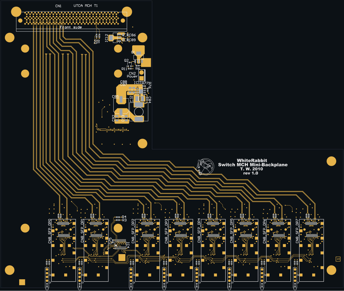
WRS V2 MINI BACKPLANE (OHWR0018 R1) is an open-hardware circuit board from the CERN Open Hardware Repository, designed in Altium Designer: a 5-layer board of 232 × 195 mm with 241 components and 201 nets, published under CERN-OHL-1.2.
review 57% walked · 10 findings: 1 blocker · 6 major · 3 minor (25 items)
Open in the interactive viewerRead the full review
Design review
Probe recorded 10 findings: 1 blocker · 6 major · 3 minor (25 items) on this design. Each is shown here with its reasoning; the full review links every one to the pins, nets and datasheet pages it rests on.
FDT434P Q1 (12 V payload switch) is driven to VGS = -12 V, beyond its ±8 V gate-source rating
FDT434P Q1, the 12 V payload switch, is driven to VGS = -12 V, beyond its +/-8 V gate-source rating, every time the MCH payload power is switched on.
Where it is
``
mermaid flowchart LR PSU["+12V_PSU"] -- "source pin 3" --> Q1["Q1 FDT434P"] -- "drain pins 2/4" --> MCH["+12V_MCH"] PSU --> R6["R6 10k"] --> G["Q1 gate pin 1<br/>NetQ1_1"] G --> Q2["Q2 BC847B collector<br/>emitter on GND"] BE["BULK_EN, CN1.170<br/>R12 10k to GND"] -- "R11 10k" --> Q2``The numbers
Quantity Value Source Source voltage 12 V netlist: +12V_PSU Gate with Q2 on about 0.1 V derived VGS about -12 V derived FDT434P VGSS absolute maximum +/-8 V (a 2.5 V-specified P-channel part) FDT434P datasheet, p.1 Why it matters
The gate oxide is overstressed whenever BULK_EN turns Q2 on. A gate-oxide overstress on the switch that feeds the MCH's 12 V payload power can fail short or open in service. A divider in the gate path (for example a resistor from the gate to Q2's collector sized to give about -5 to -7 V), or a FET rated +/-20 V VGS, fixes it.
TPS5430 IC11 ENA is tied to ground through 230 kOhm (R5 220k + R12 10k) when BULK_EN is not driven high, which the datasheet forbids; the off state sits near the 0.5 V threshold
TPS5430 IC11 ENA is tied to ground through 230 kOhm (R5 220k + R12 10k) whenever BULK_EN is not driven high, which the datasheet forbids; the off state sits at about 0.44 V, just under the 0.5 V threshold.
Where it is
``
mermaid flowchart LR ENA["IC11 TPS5430 pin 5 ENA<br/>internal 1.5 MOhm pull-up<br/>NetC91_2 with C91"] --> R5["R5 220k"] --> BE["BULK_EN<br/>MCH via CN1.170, R11"] BE --> R12["R12 10k"] --> G["GND"]``IC11 is the 12 V to +3V3 payload buck.
The numbers
Quantity Value Source ENA internal pull-up 1.5 MOhm; must not be connected with a resistor to ground, use open-drain logic TPS5430 datasheet, p.3 Resistance to GND with BULK_EN low R5 220k + R12 10k = 230k derived ENA voltage with BULK_EN low 3.3 V x 230k / 1.73M = 0.44 V derived ENA falling threshold 0.5 V (rising 1.3 V) TPS5430 datasheet, p.5 The pin sits only just under the falling threshold, inside the band where the pull-up tolerance decides, so the converter may not reliably stay off before the MCH asserts BULK_EN.
Why it matters
Payload +3V3 is meant to follow the MCH's BULK_EN; an enable that floats near threshold can bring the rail up early or chatter. An open-drain pull-down on ENA (BULK_EN inverted through a small FET) matches the datasheet's recommendation.
- ReferencePlaneDiscontinuitymajorOpen
2 nets cross one gap in POWER's negative-plane field at 2 places, the longest 0.31 mm (fastest: NetC46_2 at 100 ps 10-90 %, ASSUMED)
Along 'NetC48_2' on BOTTOM_LAYER, POWER is a negative layer (copper everywhere inside the profile), and its field is cleared for 0.31 mm under the track at (-21.3, -0.07). The layer does not state the nets either side, so whether this is a split between two planes or a void in one is not said; either way the return current has to go round it. 2 places on 2 net(s) cross it, listed below, the longest first. What cleared it: the hole at x -27.1..-19.15, y -0.14..0.11. One decision covers the void: whether these tracks may cross it, or the plane should be filled under them. No crossing has a plane on the track's other side, so the whole return meets the break.
- 'NetC48_2' on BOTTOM_LAYER at (-21.3, -0.07), 0.31 mm; other side: none: the signal layer is outermost
- 'NetC46_2' on BOTTOM_LAYER at (-21.72, -0.02), 0.25 mm; other side: none: the signal layer is outermost
Every site is a row of this finding's evidence, keyed by net, layers and position. GET /api/odb/boards/21/reference-planes?group=gap%3APOWER%3Ahole%20-27.1%2C-0.14%7C-19.15%2C0.11 serves each with its own layer_image region; all of them lie in x -22.72..-20.23, y -1.14..1.11 mm (board frame, Y up).
Read from the copper as drawn on the reference layer, along each track's centreline at exact breakpoints. The reference is the copper beside the track, never the layer's type or name. Whether it matters depends on each signal's edge rate, which nothing on file states for these nets: a slow static line crosses a split harmlessly, a fast edge does not.
At gap:POWER:hole -27.1,-0.14|-19.15,0.11
- CapVoltageDeratingmajorOpen
CapVoltageDerating: 3 components×3
e.g. “C86 sits on a 12 V rail and its voltage rating is not in the BOM”
At C86, C87, C88
Each finding, with its own headline
C86C86 sits on a 12 V rail and its voltage rating is not in the BOM
C86: on a 12 V rail but its voltage rating is not stated in the BOM — add it so the rating can be compared to the rail at all. No datasheet is on file for this part; the BOM short-spec is the source.
C87C87 sits on a 12 V rail and its voltage rating is not in the BOM
C87: on a 12 V rail but its voltage rating is not stated in the BOM — add it so the rating can be compared to the rail at all. No datasheet is on file for this part; the BOM short-spec is the source.
C88C88 sits on a 12 V rail and its voltage rating is not in the BOM
C88: on a 12 V rail but its voltage rating is not stated in the BOM — add it so the rating can be compared to the rail at all. No datasheet is on file for this part; the BOM short-spec is the source.
- DecapViaFanoutmajorOpen
DecapViaFanout: 13 components×13
e.g. “C123_SFP_DP0 on '+3V3': its rail pad reaches its via over 2.78 mm of track and its ground pad over 1.96 mm, adding about 1.39 nH to its loop, past Probe's 0.5 nH starting value; put the vias at the pads” · 4 different statements
At C121_SFP_DP2, C121_SFP_DP3, C123_SFP_DP0, C123_SFP_DP1, C123_SFP_DP2, C123_SFP_DP3 and 7 more
Each finding, with its own headline
C121_SFP_DP2C121_SFP_DP2 on '+3V3': its rail pad reaches its via over 2.21 mm of track and its ground pad over 1.37 mm, adding about 0.80 nH to its loop, past Probe's 0.5 nH starting value; put the vias at the pads
C121_SFP_DP2 on '+3V3': its rail pad reaches its via over 2.21 mm of track and its ground pad over 1.37 mm, adding about 0.80 nH to its loop, past Probe's 0.5 nH starting value; put the vias at the pads. C121_SFP_DP2.2 (rail) runs 2.21 mm along its copper to its nearest via, 1.21 mm past the 1 mm beside the pad: 0.61 nH; C121_SFP_DP2.1 (ground) runs 1.37 mm along its copper to its nearest via, 0.37 mm past the 1 mm beside the pad: 0.19 nH. Each run past the pad as one conductor of a pair 1.60 mm apart (the pad pitch), 0.2 l ln(D/R) nH with R 0.127 mm (the track's width is not read): 0.80 nH in all. Put the vias at the pads (or in them), one per pad at least, the rail's and the ground's close together; the capacitor's own inductance as mounted is 0.99 nH (pad 0.10 nH + no via of the first net within 1 mm of its pad: the study's 0.6 nH per mm of 0.64 mm depth, ASSUMED). 0.5 nH is Probe's starting value, about the whole mounted inductance of a well-mounted 0402.
C121_SFP_DP3C121_SFP_DP3 on '+3V3': its rail pad reaches its via over 1.52 mm of track and its ground pad over 1.78 mm, adding about 0.66 nH to its loop, past Probe's 0.5 nH starting value; put the vias at the pads
C121_SFP_DP3 on '+3V3': its rail pad reaches its via over 1.52 mm of track and its ground pad over 1.78 mm, adding about 0.66 nH to its loop, past Probe's 0.5 nH starting value; put the vias at the pads. C121_SFP_DP3.2 (rail) runs 1.52 mm along its copper to its nearest via, 0.52 mm past the 1 mm beside the pad: 0.26 nH; C121_SFP_DP3.1 (ground) runs 1.78 mm along its copper to its nearest via, 0.78 mm past the 1 mm beside the pad: 0.40 nH. Each run past the pad as one conductor of a pair 1.60 mm apart (the pad pitch), 0.2 l ln(D/R) nH with R 0.127 mm (the track's width is not read): 0.66 nH in all. Put the vias at the pads (or in them), one per pad at least, the rail's and the ground's close together; the capacitor's own inductance as mounted is 0.99 nH (pad 0.10 nH + no via of the first net within 1 mm of its pad: the study's 0.6 nH per mm of 0.64 mm depth, ASSUMED). 0.5 nH is Probe's starting value, about the whole mounted inductance of a well-mounted 0402.
C123_SFP_DP0C123_SFP_DP0 on '+3V3': its rail pad reaches its via over 2.78 mm of track and its ground pad over 1.96 mm, adding about 1.39 nH to its loop, past Probe's 0.5 nH starting value; put the vias at the pads
C123_SFP_DP0 on '+3V3': its rail pad reaches its via over 2.78 mm of track and its ground pad over 1.96 mm, adding about 1.39 nH to its loop, past Probe's 0.5 nH starting value; put the vias at the pads. C123_SFP_DP0.2 (rail) runs 2.78 mm along its copper to its nearest via, 1.78 mm past the 1 mm beside the pad: 0.90 nH; C123_SFP_DP0.1 (ground) runs 1.96 mm along its copper to its nearest via, 0.96 mm past the 1 mm beside the pad: 0.49 nH. Each run past the pad as one conductor of a pair 1.60 mm apart (the pad pitch), 0.2 l ln(D/R) nH with R 0.127 mm (the track's width is not read): 1.39 nH in all. Put the vias at the pads (or in them), one per pad at least, the rail's and the ground's close together; the capacitor's own inductance as mounted is 0.99 nH (pad 0.10 nH + no via of the first net within 1 mm of its pad: the study's 0.6 nH per mm of 0.64 mm depth, ASSUMED). 0.5 nH is Probe's starting value, about the whole mounted inductance of a well-mounted 0402.
C123_SFP_DP1C123_SFP_DP1 on '+3V3': its rail pad reaches its via over 2.78 mm of track and its ground pad over 1.96 mm, adding about 1.39 nH to its loop, past Probe's 0.5 nH starting value; put the vias at the pads
C123_SFP_DP1 on '+3V3': its rail pad reaches its via over 2.78 mm of track and its ground pad over 1.96 mm, adding about 1.39 nH to its loop, past Probe's 0.5 nH starting value; put the vias at the pads. C123_SFP_DP1.2 (rail) runs 2.78 mm along its copper to its nearest via, 1.78 mm past the 1 mm beside the pad: 0.90 nH; C123_SFP_DP1.1 (ground) runs 1.96 mm along its copper to its nearest via, 0.96 mm past the 1 mm beside the pad: 0.49 nH. Each run past the pad as one conductor of a pair 1.60 mm apart (the pad pitch), 0.2 l ln(D/R) nH with R 0.127 mm (the track's width is not read): 1.39 nH in all. Put the vias at the pads (or in them), one per pad at least, the rail's and the ground's close together; the capacitor's own inductance as mounted is 0.99 nH (pad 0.10 nH + no via of the first net within 1 mm of its pad: the study's 0.6 nH per mm of 0.64 mm depth, ASSUMED). 0.5 nH is Probe's starting value, about the whole mounted inductance of a well-mounted 0402.
C123_SFP_DP2C123_SFP_DP2 on '+3V3': its rail pad reaches its via over 2.78 mm of track and its ground pad over 1.96 mm, adding about 1.39 nH to its loop, past Probe's 0.5 nH starting value; put the vias at the pads
C123_SFP_DP2 on '+3V3': its rail pad reaches its via over 2.78 mm of track and its ground pad over 1.96 mm, adding about 1.39 nH to its loop, past Probe's 0.5 nH starting value; put the vias at the pads. C123_SFP_DP2.2 (rail) runs 2.78 mm along its copper to its nearest via, 1.78 mm past the 1 mm beside the pad: 0.90 nH; C123_SFP_DP2.1 (ground) runs 1.96 mm along its copper to its nearest via, 0.96 mm past the 1 mm beside the pad: 0.49 nH. Each run past the pad as one conductor of a pair 1.60 mm apart (the pad pitch), 0.2 l ln(D/R) nH with R 0.127 mm (the track's width is not read): 1.39 nH in all. Put the vias at the pads (or in them), one per pad at least, the rail's and the ground's close together; the capacitor's own inductance as mounted is 0.99 nH (pad 0.10 nH + no via of the first net within 1 mm of its pad: the study's 0.6 nH per mm of 0.64 mm depth, ASSUMED). 0.5 nH is Probe's starting value, about the whole mounted inductance of a well-mounted 0402.
C123_SFP_DP3C123_SFP_DP3 on '+3V3': its rail pad reaches its via over 2.78 mm of track and its ground pad over 1.96 mm, adding about 1.39 nH to its loop, past Probe's 0.5 nH starting value; put the vias at the pads
C123_SFP_DP3 on '+3V3': its rail pad reaches its via over 2.78 mm of track and its ground pad over 1.96 mm, adding about 1.39 nH to its loop, past Probe's 0.5 nH starting value; put the vias at the pads. C123_SFP_DP3.2 (rail) runs 2.78 mm along its copper to its nearest via, 1.78 mm past the 1 mm beside the pad: 0.90 nH; C123_SFP_DP3.1 (ground) runs 1.96 mm along its copper to its nearest via, 0.96 mm past the 1 mm beside the pad: 0.49 nH. Each run past the pad as one conductor of a pair 1.60 mm apart (the pad pitch), 0.2 l ln(D/R) nH with R 0.127 mm (the track's width is not read): 1.39 nH in all. Put the vias at the pads (or in them), one per pad at least, the rail's and the ground's close together; the capacitor's own inductance as mounted is 0.99 nH (pad 0.10 nH + no via of the first net within 1 mm of its pad: the study's 0.6 nH per mm of 0.64 mm depth, ASSUMED). 0.5 nH is Probe's starting value, about the whole mounted inductance of a well-mounted 0402.
C123_SFP_DP4C123_SFP_DP4 on '+3V3': its rail pad reaches its via over 2.78 mm of track and its ground pad over 1.96 mm, adding about 1.39 nH to its loop, past Probe's 0.5 nH starting value; put the vias at the pads
C123_SFP_DP4 on '+3V3': its rail pad reaches its via over 2.78 mm of track and its ground pad over 1.96 mm, adding about 1.39 nH to its loop, past Probe's 0.5 nH starting value; put the vias at the pads. C123_SFP_DP4.2 (rail) runs 2.78 mm along its copper to its nearest via, 1.78 mm past the 1 mm beside the pad: 0.90 nH; C123_SFP_DP4.1 (ground) runs 1.96 mm along its copper to its nearest via, 0.96 mm past the 1 mm beside the pad: 0.49 nH. Each run past the pad as one conductor of a pair 1.60 mm apart (the pad pitch), 0.2 l ln(D/R) nH with R 0.127 mm (the track's width is not read): 1.39 nH in all. Put the vias at the pads (or in them), one per pad at least, the rail's and the ground's close together; the capacitor's own inductance as mounted is 0.99 nH (pad 0.10 nH + no via of the first net within 1 mm of its pad: the study's 0.6 nH per mm of 0.64 mm depth, ASSUMED). 0.5 nH is Probe's starting value, about the whole mounted inductance of a well-mounted 0402.
C123_SFP_DP5C123_SFP_DP5 on '+3V3': its rail pad reaches its via over 2.78 mm of track and its ground pad over 1.96 mm, adding about 1.39 nH to its loop, past Probe's 0.5 nH starting value; put the vias at the pads
C123_SFP_DP5 on '+3V3': its rail pad reaches its via over 2.78 mm of track and its ground pad over 1.96 mm, adding about 1.39 nH to its loop, past Probe's 0.5 nH starting value; put the vias at the pads. C123_SFP_DP5.2 (rail) runs 2.78 mm along its copper to its nearest via, 1.78 mm past the 1 mm beside the pad: 0.90 nH; C123_SFP_DP5.1 (ground) runs 1.96 mm along its copper to its nearest via, 0.96 mm past the 1 mm beside the pad: 0.49 nH. Each run past the pad as one conductor of a pair 1.60 mm apart (the pad pitch), 0.2 l ln(D/R) nH with R 0.127 mm (the track's width is not read): 1.39 nH in all. Put the vias at the pads (or in them), one per pad at least, the rail's and the ground's close together; the capacitor's own inductance as mounted is 0.99 nH (pad 0.10 nH + no via of the first net within 1 mm of its pad: the study's 0.6 nH per mm of 0.64 mm depth, ASSUMED). 0.5 nH is Probe's starting value, about the whole mounted inductance of a well-mounted 0402.
C123_SFP_DP6C123_SFP_DP6 on '+3V3': its rail pad reaches its via over 2.78 mm of track and its ground pad over 1.96 mm, adding about 1.39 nH to its loop, past Probe's 0.5 nH starting value; put the vias at the pads
C123_SFP_DP6 on '+3V3': its rail pad reaches its via over 2.78 mm of track and its ground pad over 1.96 mm, adding about 1.39 nH to its loop, past Probe's 0.5 nH starting value; put the vias at the pads. C123_SFP_DP6.2 (rail) runs 2.78 mm along its copper to its nearest via, 1.78 mm past the 1 mm beside the pad: 0.90 nH; C123_SFP_DP6.1 (ground) runs 1.96 mm along its copper to its nearest via, 0.96 mm past the 1 mm beside the pad: 0.49 nH. Each run past the pad as one conductor of a pair 1.60 mm apart (the pad pitch), 0.2 l ln(D/R) nH with R 0.127 mm (the track's width is not read): 1.39 nH in all. Put the vias at the pads (or in them), one per pad at least, the rail's and the ground's close together; the capacitor's own inductance as mounted is 0.99 nH (pad 0.10 nH + no via of the first net within 1 mm of its pad: the study's 0.6 nH per mm of 0.64 mm depth, ASSUMED). 0.5 nH is Probe's starting value, about the whole mounted inductance of a well-mounted 0402.
C123_SFP_DP7C123_SFP_DP7 on '+3V3': its rail pad reaches its via over 2.78 mm of track and its ground pad over 1.96 mm, adding about 1.39 nH to its loop, past Probe's 0.5 nH starting value; put the vias at the pads
C123_SFP_DP7 on '+3V3': its rail pad reaches its via over 2.78 mm of track and its ground pad over 1.96 mm, adding about 1.39 nH to its loop, past Probe's 0.5 nH starting value; put the vias at the pads. C123_SFP_DP7.2 (rail) runs 2.78 mm along its copper to its nearest via, 1.78 mm past the 1 mm beside the pad: 0.90 nH; C123_SFP_DP7.1 (ground) runs 1.96 mm along its copper to its nearest via, 0.96 mm past the 1 mm beside the pad: 0.49 nH. Each run past the pad as one conductor of a pair 1.60 mm apart (the pad pitch), 0.2 l ln(D/R) nH with R 0.127 mm (the track's width is not read): 1.39 nH in all. Put the vias at the pads (or in them), one per pad at least, the rail's and the ground's close together; the capacitor's own inductance as mounted is 0.99 nH (pad 0.10 nH + no via of the first net within 1 mm of its pad: the study's 0.6 nH per mm of 0.64 mm depth, ASSUMED). 0.5 nH is Probe's starting value, about the whole mounted inductance of a well-mounted 0402.
C80_SFP_DP0C80_SFP_DP0 on '+3V3': its rail pad reaches its via over 1.79 mm of track and its ground pad over 1.51 mm, adding about 0.66 nH to its loop, past Probe's 0.5 nH starting value; put the vias at the pads
C80_SFP_DP0 on '+3V3': its rail pad reaches its via over 1.79 mm of track and its ground pad over 1.51 mm, adding about 0.66 nH to its loop, past Probe's 0.5 nH starting value; put the vias at the pads. C80_SFP_DP0.2 (rail) runs 1.79 mm along its copper to its nearest via, 0.79 mm past the 1 mm beside the pad: 0.40 nH; C80_SFP_DP0.1 (ground) runs 1.51 mm along its copper to its nearest via, 0.51 mm past the 1 mm beside the pad: 0.26 nH. Each run past the pad as one conductor of a pair 1.60 mm apart (the pad pitch), 0.2 l ln(D/R) nH with R 0.127 mm (the track's width is not read): 0.66 nH in all. Put the vias at the pads (or in them), one per pad at least, the rail's and the ground's close together; the capacitor's own inductance as mounted is 0.99 nH (pad 0.10 nH + no via of the first net within 1 mm of its pad: the study's 0.6 nH per mm of 0.64 mm depth, ASSUMED). 0.5 nH is Probe's starting value, about the whole mounted inductance of a well-mounted 0402.
C80_SFP_DP2C80_SFP_DP2 on '+3V3': its rail pad reaches its via over 1.79 mm of track and its ground pad over 1.51 mm, adding about 0.66 nH to its loop, past Probe's 0.5 nH starting value; put the vias at the pads
C80_SFP_DP2 on '+3V3': its rail pad reaches its via over 1.79 mm of track and its ground pad over 1.51 mm, adding about 0.66 nH to its loop, past Probe's 0.5 nH starting value; put the vias at the pads. C80_SFP_DP2.2 (rail) runs 1.79 mm along its copper to its nearest via, 0.79 mm past the 1 mm beside the pad: 0.40 nH; C80_SFP_DP2.1 (ground) runs 1.51 mm along its copper to its nearest via, 0.51 mm past the 1 mm beside the pad: 0.26 nH. Each run past the pad as one conductor of a pair 1.60 mm apart (the pad pitch), 0.2 l ln(D/R) nH with R 0.127 mm (the track's width is not read): 0.66 nH in all. Put the vias at the pads (or in them), one per pad at least, the rail's and the ground's close together; the capacitor's own inductance as mounted is 0.99 nH (pad 0.10 nH + no via of the first net within 1 mm of its pad: the study's 0.6 nH per mm of 0.64 mm depth, ASSUMED). 0.5 nH is Probe's starting value, about the whole mounted inductance of a well-mounted 0402.
C80_SFP_DP4C80_SFP_DP4 on '+3V3': its rail pad reaches its via over 1.79 mm of track and its ground pad over 1.51 mm, adding about 0.66 nH to its loop, past Probe's 0.5 nH starting value; put the vias at the pads
C80_SFP_DP4 on '+3V3': its rail pad reaches its via over 1.79 mm of track and its ground pad over 1.51 mm, adding about 0.66 nH to its loop, past Probe's 0.5 nH starting value; put the vias at the pads. C80_SFP_DP4.2 (rail) runs 1.79 mm along its copper to its nearest via, 0.79 mm past the 1 mm beside the pad: 0.40 nH; C80_SFP_DP4.1 (ground) runs 1.51 mm along its copper to its nearest via, 0.51 mm past the 1 mm beside the pad: 0.26 nH. Each run past the pad as one conductor of a pair 1.60 mm apart (the pad pitch), 0.2 l ln(D/R) nH with R 0.127 mm (the track's width is not read): 0.66 nH in all. Put the vias at the pads (or in them), one per pad at least, the rail's and the ground's close together; the capacitor's own inductance as mounted is 0.99 nH (pad 0.10 nH + no via of the first net within 1 mm of its pad: the study's 0.6 nH per mm of 0.64 mm depth, ASSUMED). 0.5 nH is Probe's starting value, about the whole mounted inductance of a well-mounted 0402.
- PartLifecyclemajorOpen
FDT434P on Q1: the distributor catalogue reports "Obsolete" for onsemi's FDT434P
FDT434P on Q1: the distributor catalogue reports "Obsolete" for onsemi's FDT434P — a sourcing/longevity risk to confirm against the MANUFACTURER before acting. This board's BOM names no manufacturer for it, so whether that is the fitted maker's product was not checked. A distributor delisting is not the same claim as the part being unavailable; check the vendor's own lifecycle/product-change notice for the status and any named successor. Re-read the source: GET /api/odb/parts/FDT434P/providers (which provider said it, the maker and part number it matched, its own words, and when we asked). THE LAST BUY DATE HAS PASSED (2019-01-26, 2,850 day(s) ago), so this is a substitution rather than a buy. The distributor reports NONE left. No approved alternate is recorded for this position.
At Q1
- FiducialMissingmajorOpen
FiducialMissing: 2 boards×2
Checked by the review, stands · Claude walker (cern session) — No fiducial on this board: none of the 241 BOM rows is a FID*/FTG*/fiducial part and the rule found no fiducial-attribute pad. Not refuted; whether a production panel carries them is for the owner.
At bottom, top
Each finding, with its own headline
bottomThe bottom side carries 15 SMT component(s) and no fiducial was found on it
The bottom side carries 15 SMT component(s) but no fiducial was found on it — a placement machine has no optical reference to align to. Probe found no pad labelled .pad_usage=g_fiducial/l_fiducial (basis pad_usage); no single-pad, netless, undrilled component whose 0.5-3 mm round pad has a concentric solder-mask opening at least 1.5x its diameter with no other copper inside it (basis geometry); and no component whose refdes starts FID or whose part or package name contains FIDUCIAL (basis footprint-name). If your library names fiducials something Probe does not recognise, mark this benign — disposition_finding(rule='FiducialMissing', entity='bottom', status='benign', reason=…) — the name match only ever silences this check, it never asserts anything. If the side really has no fiducial, say so with status='confirmed': that answers the finding and keeps it gating release.
topThe top side carries 24 SMT component(s) and no fiducial was found on it
The top side carries 24 SMT component(s) but no fiducial was found on it — a placement machine has no optical reference to align to. Probe found no pad labelled .pad_usage=g_fiducial/l_fiducial (basis pad_usage); no single-pad, netless, undrilled component whose 0.5-3 mm round pad has a concentric solder-mask opening at least 1.5x its diameter with no other copper inside it (basis geometry); and no component whose refdes starts FID or whose part or package name contains FIDUCIAL (basis footprint-name). If your library names fiducials something Probe does not recognise, mark this benign — disposition_finding(rule='FiducialMissing', entity='top', status='benign', reason=…) — the name match only ever silences this check, it never asserts anything. If the side really has no fiducial, say so with status='confirmed': that answers the finding and keeps it gating release.
Mini-backplane LVDS buffer enables float at power-up while several DS90LV001 outputs share one bus (FB_MUXED, FB_01..FB_67)
Several DS90LV001 LVDS buffers drive shared buses (FB_MUXED, FB_01..FB_67), and every enable comes only from a PCA9534/PCA9534A port with no pull resistor, so at power-up all enables float and any number of drivers can be on one pair.
Where it is
``
mermaid flowchart LR IC8["IC8 PCA9534A<br/>pins 4-7, inputs at power-on"] -- "BUF_EN0-3, no pull" --> B["IC5, IC6, IC7, IC13<br/>EN pin 8"] B -- "pins 7 / 6" --> FB["FB_MUXED_P/N"] X["IC8_SFP_DPx expanders"] -- "EN_FB_RX / TX, no pull" --> P["IC9_SFP_DP0, IC9_SFP_DP1<br/>EN pin 8"] P -- "pins 7 / 6" --> F01["FB_01_P/N"]``- IC5, IC6, IC7 and IC13 all drive FB_MUXED.
- Each pair of per-port buffers (IC9_SFP_DPx) drives a shared FB_01 / FB_23 / FB_45 / FB_67 net.
- The expanders power up with all ports as inputs (PCA9534 datasheet, p.1), so every EN floats until firmware configures them.
Why it matters
LVDS drivers are current-limited, so contention is more a signal-integrity and supply-current issue than a damage risk. A pull-down on each EN (or on the shared enable nets) makes power-up deterministic.
BC847B went end-of-life (Not For New Designs)
Vendor (DigiKey) lifecycle for BC847B (Nexperia USA Inc.'s listing) changed from "Active" to "Not For New Designs" since this board was reviewed. Placed as Q2. A sourcing/longevity risk; consider a replacement before production.
- concernCON-001minorOpen
[eol:BC847B:Not For New Designs] BC847B lifecycle changed from "Active" to "Not For New Designs" since this board was reviewed: OHWR0018 R1 WRS V2 MINI BACKPLANE. A sourcing and longevity risk. Should this be replaced before the next build?
Main parts
| Part number | Maker | Description | Where |
|---|---|---|---|
| BC847B | Transistor | Q2 | |
| FDT434P | P-Channel MOSFET | Q1 | |
| LM1117-3.3 | Three-Terminal Adjustable Output Positive Voltage Regulator | IC12 | |
| PCA9534A | 8-bit I2C I/O expander | IC8 | |
| PCA9548A | 1-to-8 I2C bus mux | IC4 | |
| Power | Header, 2-Pin | CN2 | |
| RSX510L-20 | Schottky Diode | D1 | |
| TPS5430 | Step-down switchmode converter | IC11 | |
| UTCA MCH T1 | microTCA MTCA.0 MCH socket (AMC0.0 B+ connector with reversed pins) | CN1 | |
| 571-0112-100F | 2x LED Botom Green, Top Red | LD1_SFP_DP0, LD1_SFP_DP1, LD1_SFP_DP2, LD1_SFP_DP3, LD1_SFP_DP4, LD1_SFP_DP5, LD1_SFP_DP6, LD1_SFP_DP7 | |
| PCA9534 | 8-bit I2C I/O expander | IC8_SFP_DP0, IC8_SFP_DP1, IC8_SFP_DP2, IC8_SFP_DP3, IC8_SFP_DP4, IC8_SFP_DP5, IC8_SFP_DP6, IC8_SFP_DP7 | |
| DS90LV001 | LVDS buffer with enable | IC10_SFP_DP0, IC10_SFP_DP1, IC10_SFP_DP2, IC10_SFP_DP3, IC10_SFP_DP4, IC10_SFP_DP5 and 14 more |
About this design
- Design
- WRS V2 MINI BACKPLANE — OHWR0018 R1
- Designed in
- Altium Designer
- Board
- 5 copper layers, 232 × 195 mm, 241 components, 201 nets
- Licence
- CERN-OHL-1.2
- Source
- https://gitlab.com/ohwr/project/wr-switch-hw at commit
54f8a604978b - Attribution
- CERN Open Hardware Repository, project ohwr/project/wr-switch-hw (commit 54f8a604978bdc65bbde5b1f4c7ec9bee3505a44, 2025-04-09). Licence: CERN-OHL-1.2. Source: https://gitlab.com/ohwr/project/wr-switch-hw. This is a snapshot of the copy published on the OHWR GitLab pages (R1), not CERN's released record. CERN's source of truth is EDMS (https://edms.cern.ch), and the current release may be newer.
- Reviewed with
- Probe by E# (E-Sharp AB)