 Probe

WRS V3 BACKPLANE 18SFP
OHWR0013 · revision R1
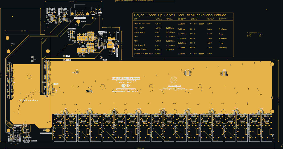
WRS V3 BACKPLANE 18SFP (OHWR0013 R1) is an open-hardware circuit board from the CERN Open Hardware Repository, designed in Altium Designer: a 6-layer board of 439.1 × 218 mm with 511 components and 467 nets, published under CERN-OHL-1.2.
review 92% walked · 17 findings: 1 blocker · 9 major · 7 minor (90 items)
Open in the interactive viewerRead the full review
Design review
Probe recorded 17 findings: 1 blocker · 9 major · 7 minor (90 items) on this design. Each is shown here with its reasoning; the full review links every one to the pins, nets and datasheet pages it rests on.
- NetCopperSplitblockerOpen
CHASSIS's copper is in 56 pieces: IC3.1, IC9.1, J3.10, J3.11, J4.6, J9.6, L7.2, S2.3 and 3 more pin(s) and 54 other piece(s) are not connected to the rest of the net
CHASSIS's copper is in 56 pieces: IC3.1, IC9.1, J3.10, J3.11, J4.6, J9.6, L7.2, S2.3 and 3 more pin(s) and 54 other piece(s) are not connected to the rest of the net. Piece 1: C41.1, IC1.1, J10-1.24, J10-1.25, J10-1.26, J10-1.27, J10-1.28, J10-1.29 and 139 more pin(s), on TOP_LAYER, MID-LAYER_1, MID-LAYER_2 and BOTTOM_LAYER, 150 drill(s), 11001.89 mm2 of pour, over (1.07, 0.36) to (434.62, 28.38). Piece 2: IC3.1, IC9.1, J3.10, J3.11, J4.6, J9.6, L7.2, S2.3 and 3 more pin(s), on TOP_LAYER, MID-LAYER_1, MID-LAYER_2 and BOTTOM_LAYER, 17 drill(s), 3383.57 mm2 of pour, over (65.99, 178.33) to (156.79, 217.82). Piece 3: J10-5.23, on TOP_LAYER, MID-LAYER_1, MID-LAYER_2 and BOTTOM_LAYER, 1 drill(s), over (253.07, 30.69) to (255.07, 32.69). Piece 4: J10-5.22, on TOP_LAYER, MID-LAYER_1, MID-LAYER_2 and BOTTOM_LAYER, 1 drill(s), over (253.07, 40.69) to (255.07, 42.69). Piece 5: J8-5.21, on TOP_LAYER, MID-LAYER_1, MID-LAYER_2 and BOTTOM_LAYER, 1 drill(s), over (258.63, 35.69) to (260.63, 37.69). Piece 6: J8-5.23, on TOP_LAYER, MID-LAYER_1, MID-LAYER_2 and BOTTOM_LAYER, 1 drill(s), over (272.88, 30.69) to (274.88, 32.69). Piece 7: J8-5.22, on TOP_LAYER, MID-LAYER_1, MID-LAYER_2 and BOTTOM_LAYER, 1 drill(s), over (272.88, 40.69) to (274.88, 42.69). Piece 8: J10-6.21, on TOP_LAYER, MID-LAYER_1, MID-LAYER_2 and BOTTOM_LAYER, 1 drill(s), over (278.56, 35.69) to (280.56, 37.69). Piece 9: J10-6.23, on TOP_LAYER, MID-LAYER_1, MID-LAYER_2 and BOTTOM_LAYER, 1 drill(s), over (292.81, 30.69) to (294.81, 32.69). Piece 10: J10-6.22, on TOP_LAYER, MID-LAYER_1, MID-LAYER_2 and BOTTOM_LAYER, 1 drill(s), over (292.81, 40.69) to (294.81, 42.69). Piece 11: J8-6.21, on TOP_LAYER, MID-LAYER_1, MID-LAYER_2 and BOTTOM_LAYER, 1 drill(s), over (298.37, 35.69) to (300.37, 37.69). Piece 12: J8-6.23, on TOP_LAYER, MID-LAYER_1, MID-LAYER_2 and BOTTOM_LAYER, 1 drill(s), over (312.62, 30.69) to (314.62, 32.69). Piece 13: J8-6.22, on TOP_LAYER, MID-LAYER_1, MID-LAYER_2 and BOTTOM_LAYER, 1 drill(s), over (312.62, 40.69) to (314.62, 42.69). Piece 14: J10-7.21, on TOP_LAYER, MID-LAYER_1, MID-LAYER_2 and BOTTOM_LAYER, 1 drill(s), over (318.31, 35.69) to (320.31, 37.69). Piece 15: J10-7.23, on TOP_LAYER, MID-LAYER_1, MID-LAYER_2 and BOTTOM_LAYER, 1 drill(s), over (332.56, 30.69) to (334.56, 32.69). Piece 16: J10-7.22, on TOP_LAYER, MID-LAYER_1, MID-LAYER_2 and BOTTOM_LAYER, 1 drill(s), over (332.56, 40.69) to (334.56, 42.69). Piece 17: J8-7.21, on TOP_LAYER, MID-LAYER_1, MID-LAYER_2 and BOTTOM_LAYER, 1 drill(s), over (338.13, 35.69) to (340.13, 37.69). Piece 18: J8-7.23, on TOP_LAYER, MID-LAYER_1, MID-LAYER_2 and BOTTOM_LAYER, 1 drill(s), over (352.38, 30.69) to (354.38, 32.69). Piece 19: J8-7.22, on TOP_LAYER, MID-LAYER_1, MID-LAYER_2 and BOTTOM_LAYER, 1 drill(s), over (352.38, 40.69) to (354.38, 42.69). Piece 20: J10-8.21, on TOP_LAYER, MID-LAYER_1, MID-LAYER_2 and BOTTOM_LAYER, 1 drill(s), over (358.06, 35.69) to (360.06, 37.69). Piece 21: J10-8.23, on TOP_LAYER, MID-LAYER_1, MID-LAYER_2 and BOTTOM_LAYER, 1 drill(s), over (372.31, 30.69) to (374.31, 32.69). Piece 22: J10-8.22, on TOP_LAYER, MID-LAYER_1, MID-LAYER_2 and BOTTOM_LAYER, 1 drill(s), over (372.31, 40.69) to (374.31, 42.69). Piece 23: J8-8.21, on TOP_LAYER, MID-LAYER_1, MID-LAYER_2 and BOTTOM_LAYER, 1 drill(s), over (377.88, 35.69) to (379.88, 37.69). Piece 24: J8-8.23, on TOP_LAYER, MID-LAYER_1, MID-LAYER_2 and BOTTOM_LAYER, 1 drill(s), over (392.13, 30.69) to (394.13, 32.69). Piece 25: J8-8.22, on TOP_LAYER, MID-LAYER_1, MID-LAYER_2 and BOTTOM_LAYER, 1 drill(s), over (392.13, 40.69) to (394.13, 42.69). Piece 26: J10-9.21, on TOP_LAYER, MID-LAYER_1, MID-LAYER_2 and BOTTOM_LAYER, 1 drill(s), over (397.82, 35.69) to (399.82, 37.69). Piece 27: J10-9.23, on TOP_LAYER, MID-LAYER_1, MID-LAYER_2 and BOTTOM_LAYER, 1 drill(s), over (412.07, 30.69) to (414.07, 32.69). Piece 28: J10-9.22, on TOP_LAYER, MID-LAYER_1, MID-LAYER_2 and BOTTOM_LAYER, 1 drill(s), over (412.07, 40.69) to (414.07, 42.69). Piece 29: J8-9.21, on TOP_LAYER, MID-LAYER_1, MID-LAYER_2 and BOTTOM_LAYER, 1 drill(s), over (417.63, 35.69) to (419.63, 37.69). Piece 30: J8-9.23, on TOP_LAYER, MID-LAYER_1, MID-LAYER_2 and BOTTOM_LAYER, 1 drill(s), over (431.88, 30.69) to (433.88, 32.69). Piece 31: J8-9.22, on TOP_LAYER, MID-LAYER_1, MID-LAYER_2 and BOTTOM_LAYER, 1 drill(s), over (431.88, 40.69) to (433.88, 42.69). Piece 32: J10-1.21, on TOP_LAYER, MID-LAYER_1, MID-LAYER_2 and BOTTOM_LAYER, 1 drill(s), over (79.91, 35.69) to (81.91, 37.69). Piece 33: J10-1.23, on TOP_LAYER, MID-LAYER_1, MID-LAYER_2 and BOTTOM_LAYER, 1 drill(s), over (94.16, 30.69) to (96.16, 32.69). Piece 34: J10-1.22, on TOP_LAYER, MID-LAYER_1, MID-LAYER_2 and BOTTOM_LAYER, 1 drill(s), over (94.16, 40.69) to (96.16, 42.69). Piece 35: J8-1.21, on TOP_LAYER, MID-LAYER_1, MID-LAYER_2 and BOTTOM_LAYER, 1 drill(s), over (99.72, 35.69) to (101.72, 37.69). Piece 36: J8-1.23, on TOP_LAYER, MID-LAYER_1, MID-LAYER_2 and BOTTOM_LAYER, 1 drill(s), over (113.97, 30.69) to (115.97, 32.69). Piece 37: J8-1.22, on TOP_LAYER, MID-LAYER_1, MID-LAYER_2 and BOTTOM_LAYER, 1 drill(s), over (113.97, 40.69) to (115.97, 42.69). Piece 38: J10-2.21, on TOP_LAYER, MID-LAYER_1, MID-LAYER_2 and BOTTOM_LAYER, 1 drill(s), over (119.57, 35.69) to (121.57, 37.69). Piece 39: J10-2.23, on TOP_LAYER, MID-LAYER_1, MID-LAYER_2 and BOTTOM_LAYER, 1 drill(s), over (133.82, 30.69) to (135.82, 32.69). Piece 40: J10-2.22, on TOP_LAYER, MID-LAYER_1, MID-LAYER_2 and BOTTOM_LAYER, 1 drill(s), over (133.82, 40.69) to (135.82, 42.69). Piece 41: J8-2.21, on TOP_LAYER, MID-LAYER_1, MID-LAYER_2 and BOTTOM_LAYER, 1 drill(s), over (139.38, 35.69) to (141.38, 37.69). Piece 42: J8-2.23, on TOP_LAYER, MID-LAYER_1, MID-LAYER_2 and BOTTOM_LAYER, 1 drill(s), over (153.63, 30.69) to (155.63, 32.69). Piece 43: J8-2.22, on TOP_LAYER, MID-LAYER_1, MID-LAYER_2 and BOTTOM_LAYER, 1 drill(s), over (153.63, 40.69) to (155.63, 42.69). Piece 44: J10-3.21, on TOP_LAYER, MID-LAYER_1, MID-LAYER_2 and BOTTOM_LAYER, 1 drill(s), over (159.26, 35.69) to (161.26, 37.69). Piece 45: J10-3.23, on TOP_LAYER, MID-LAYER_1, MID-LAYER_2 and BOTTOM_LAYER, 1 drill(s), over (173.51, 30.69) to (175.51, 32.69). Piece 46: J10-3.22, on TOP_LAYER, MID-LAYER_1, MID-LAYER_2 and BOTTOM_LAYER, 1 drill(s), over (173.51, 40.69) to (175.51, 42.69). Piece 47: J8-3.21, on TOP_LAYER, MID-LAYER_1, MID-LAYER_2 and BOTTOM_LAYER, 1 drill(s), over (179.13, 35.69) to (181.13, 37.69). Piece 48: J8-3.23, on TOP_LAYER, MID-LAYER_1, MID-LAYER_2 and BOTTOM_LAYER, 1 drill(s), over (193.38, 30.69) to (195.38, 32.69). Piece 49: J8-3.22, on TOP_LAYER, MID-LAYER_1, MID-LAYER_2 and BOTTOM_LAYER, 1 drill(s), over (193.38, 40.69) to (195.38, 42.69). Piece 50: J10-4.21, on TOP_LAYER, MID-LAYER_1, MID-LAYER_2 and BOTTOM_LAYER, 1 drill(s), over (199.07, 35.69) to (201.07, 37.69). Piece 51: J10-4.23, on TOP_LAYER, MID-LAYER_1, MID-LAYER_2 and BOTTOM_LAYER, 1 drill(s), over (213.32, 30.69) to (215.32, 32.69). Piece 52: J10-4.22, on TOP_LAYER, MID-LAYER_1, MID-LAYER_2 and BOTTOM_LAYER, 1 drill(s), over (213.32, 40.69) to (215.32, 42.69). Piece 53: J8-4.21, on TOP_LAYER, MID-LAYER_1, MID-LAYER_2 and BOTTOM_LAYER, 1 drill(s), over (218.88, 35.69) to (220.88, 37.69). Piece 54: J8-4.23, on TOP_LAYER, MID-LAYER_1, MID-LAYER_2 and BOTTOM_LAYER, 1 drill(s), over (233.13, 30.69) to (235.13, 32.69). Piece 55: J8-4.22, on TOP_LAYER, MID-LAYER_1, MID-LAYER_2 and BOTTOM_LAYER, 1 drill(s), over (233.13, 40.69) to (235.13, 42.69). Piece 56: J10-5.21, on TOP_LAYER, MID-LAYER_1, MID-LAYER_2 and BOTTOM_LAYER, 1 drill(s), over (238.82, 35.69) to (240.82, 37.69). The export files every one of these pins under the net, so every connectivity check passes; the copper the fab builds leaves them apart. Usually a pour island that touches only one via of its own net, or a track ending short of its copper: join the piece to the net and export again.
At split:CHASSIS
Fan switches Q3/Q4 (DMP2066LSN, VGSS ±12 V): on the PCB the gate is pulled straight to GND by Q1/Q2, so VGS reaches the full +12VCC_IN; the schematic's 4K7 gate divider (R64/R65) was never placed
The fan switches Q3/Q4 (DMP2066LSN, VGSS +/-12 V) have their gate pulled straight to GND by Q1/Q2 on the PCB, so VGS reaches the full +12VCC_IN; the schematic's 4K7 gate divider R64/R65 was never placed.
As built
J11 (FAN_PSU) and J5 (FAN_BOX) are switched from +12VCC_IN by the P-channel MOSFETs Q3 and Q4 (DMP2066LSN-7).
``
mermaid flowchart LR VIN["+12VCC_IN"] -- "R60 / R4 4K7 pull-up" --> G["gate net<br/>NetQ1_2 / NetQ2_2"] VIN --> S["Q3 / Q4 source"] G --> Q3["Q3 / Q4 DMP2066LSN<br/>VGSS +/-12 V"] S --> Q3 EN["FAN_PSU_EN / FAN_BOX_EN"] --> Q1["Q1 / Q2 DMN2020LSN<br/>drain on gate net"] Q1 -- "pulls gate to about 0 V" --> G Q3 --> FAN["J11 / J5 fan outputs"]``When the driver turns on, the gate goes to about 0 V while the source sits on +12VCC_IN, so |VGS| equals the input rail.
The numbers
Quantity Value Source DMP2066LSN gate-source voltage, absolute maximum +/-12 V DMP2066LSN datasheet, p.1 VGS when the driver is on = +12VCC_IN netlist: NetQ1_2, NetQ2_2 VGS with the schematic's R64/R65 divider about 6 V derived What the schematic intended
The schematic on file (Connectors_GPIOs sheet) draws R64 and R65 (4K7) between the driver drain and the P-FET gate, which would halve the drive to about 6 V, and R62/R63 (1R0) in series with the fan outputs. None of R62-R65 exists in the PCB or its BOM (511 placed parts, BOM generated from the PcbDoc).
Schematic and PCB disagree at the same repository commit: R62-R67 are drawn but not on the board, and R42 is 10K on the schematic but 4K7 on the PCB/BOM
At commit 54f8a60 of wr-switch-hw (mini_backplane_18SFP), the schematic and the PCB describe different boards: R62-R67 are drawn but not placed, and R42 is 10K on the schematic but 4K7 on the PCB/BOM.
The differences
Part Schematic PCB / BOM (generated from the PcbDoc, 511 placed parts) R62, R63 1R0, in series with fan outputs J11/J5 (Connectors_GPIOs, sheet 11) absent R64, R65 4K7, P-FET gate drive of Q3/Q4 (sheet 11) absent R66, R67 0R, on the I2C_TP lines (I2C_Peripherals, sheet 13) absent R42 (TPS53126 TRIP2 resistor) 10K (Power_Supply, sheet 15) 4K7 Why it matters
A reader of the published schematic sees a gate divider, series resistors and an over-current setting that the fabricated board does not have.
- ReferencePlaneDiscontinuitymajorOpen
162 nets change reference between +3V3 and GND at 217 vias; 202 of them partial (fastest: FPGA-GPIO36 at 100 ps 10-90 %, ASSUMED)
At 217 via(s), on 162 net(s), the signal leaves a layer referenced by one of +3V3 and GND for a layer referenced by the other, and no plane references both layers. Different nets: no via can carry the return across; only decoupling between the two planes near the via can. The capacitor carrying the return across was measured at each via, at the knee of the crossing net's edge against 50 ohm assumed: 217 with none. 217 of them at an ASSUMED edge (no edge on file for the net): state one (net_timing_state) and it is re-read. One decision covers the pair: whether +3V3 and GND are decoupled to each other near these vias. A via whose layers have more references than these two is a site of each pair it joins. 202 of them are partial: another reference continues across through a stitching via of its net, so only part of the return has nowhere to go. The pure ones are listed first, then the partial ones with the farthest stitching via first.
- 'MGTTX112_0_P' at (66.1, 131), TOP_LAYER -> MID-LAYER_2: GND on MID-LAYER_1 to +3V3 on PWR, GND on BOTTOM_LAYER; partial, GND continues through a via of GND 2.4 mm away; stitching none, 455.1 mm of track past the via on MID-LAYER_2: At the 5 GHz knee of a 100 ps edge (100 ps 10-90 %, assumed: no edge is on file for the net) no capacitor carries the return; only the planes do. +3V3 and GND are not a thin pair (at most 0.2 mm), so their own capacitance does not carry the return. To serve it, change layers across the same plane, or move the signal to a layer referenced to ground. None.
- 'MGTTX112_0_N' at (65.2, 131.5), TOP_LAYER -> MID-LAYER_2: GND on MID-LAYER_1 to +3V3 on PWR, GND on BOTTOM_LAYER; partial, GND continues through a via of GND 3.23 mm away; stitching none, 450.6 mm of track past the via on MID-LAYER_2: At the 5 GHz knee of a 100 ps edge (100 ps 10-90 %, assumed: no edge is on file for the net) no capacitor carries the return; only the planes do. +3V3 and GND are not a thin pair (at most 0.2 mm), so their own capacitance does not carry the return. To serve it, change layers across the same plane, or move the signal to a layer referenced to ground. None.
- 'MGTTX112_1_P' at (66.19, 129.54), TOP_LAYER -> MID-LAYER_2: GND on MID-LAYER_1 to +3V3 on PWR, GND on BOTTOM_LAYER; partial, GND continues through a via of GND 3.03 mm away; stitching none, 428.6 mm of track past the via on MID-LAYER_2: At the 5 GHz knee of a 100 ps edge (100 ps 10-90 %, assumed: no edge is on file for the net) no capacitor carries the return; only the planes do. +3V3 and GND are not a thin pair (at most 0.2 mm), so their own capacitance does not carry the return. To serve it, change layers across the same plane, or move the signal to a layer referenced to ground. None.
- 'MGTTX112_1_N' at (66.19, 128.52), TOP_LAYER -> MID-LAYER_2: GND on MID-LAYER_1 to +3V3 on PWR, GND on BOTTOM_LAYER; partial, GND continues through a via of GND 3.74 mm away; stitching none, 428.3 mm of track past the via on MID-LAYER_2: At the 5 GHz knee of a 100 ps edge (100 ps 10-90 %, assumed: no edge is on file for the net) no capacitor carries the return; only the planes do. +3V3 and GND are not a thin pair (at most 0.2 mm), so their own capacitance does not carry the return. To serve it, change layers across the same plane, or move the signal to a layer referenced to ground. None.
- 'MGTTX112_2_P' at (66.19, 127.51), TOP_LAYER -> MID-LAYER_2: GND on MID-LAYER_1 to +3V3 on PWR, GND on BOTTOM_LAYER; partial, GND continues through a via of GND 2.99 mm away; stitching none, 408.0 mm of track past the via on MID-LAYER_2: At the 5 GHz knee of a 100 ps edge (100 ps 10-90 %, assumed: no edge is on file for the net) no capacitor carries the return; only the planes do. +3V3 and GND are not a thin pair (at most 0.2 mm), so their own capacitance does not carry the return. To serve it, change layers across the same plane, or move the signal to a layer referenced to ground. None.
- 'MGTTX112_2_N' at (66.19, 126.49), TOP_LAYER -> MID-LAYER_2: GND on MID-LAYER_1 to +3V3 on PWR, GND on BOTTOM_LAYER; partial, GND continues through a via of GND 2.44 mm away; stitching none, 406.3 mm of track past the via on MID-LAYER_2: At the 5 GHz knee of a 100 ps edge (100 ps 10-90 %, assumed: no edge is on file for the net) no capacitor carries the return; only the planes do. +3V3 and GND are not a thin pair (at most 0.2 mm), so their own capacitance does not carry the return. To serve it, change layers across the same plane, or move the signal to a layer referenced to ground. None.
- 'MGTTX112_3_P' at (66.19, 125.48), TOP_LAYER -> MID-LAYER_2: GND on MID-LAYER_1 to +3V3 on PWR, GND on BOTTOM_LAYER; partial, GND continues through a via of GND 2.24 mm away; stitching none, 384.8 mm of track past the via on MID-LAYER_2: At the 5 GHz knee of a 100 ps edge (100 ps 10-90 %, assumed: no edge is on file for the net) no capacitor carries the return; only the planes do. +3V3 and GND are not a thin pair (at most 0.2 mm), so their own capacitance does not carry the return. To serve it, change layers across the same plane, or move the signal to a layer referenced to ground. None.
- 'MGTTX112_3_N' at (66.19, 124.46), TOP_LAYER -> MID-LAYER_2: GND on MID-LAYER_1 to +3V3 on PWR, GND on BOTTOM_LAYER; partial, GND continues through a via of GND 2.47 mm away; stitching none, 383.9 mm of track past the via on MID-LAYER_2: At the 5 GHz knee of a 100 ps edge (100 ps 10-90 %, assumed: no edge is on file for the net) no capacitor carries the return; only the planes do. +3V3 and GND are not a thin pair (at most 0.2 mm), so their own capacitance does not carry the return. To serve it, change layers across the same plane, or move the signal to a layer referenced to ground. None.
- 'FPGA-GPIO39' at (377.8, 80.4), MID-LAYER_1 -> MID-LAYER_2: GND on TOP_LAYER, GND on GND to +3V3 on PWR, GND on BOTTOM_LAYER; partial, GND continues through a via of GND 28.41 mm away; stitching none, 382.8 mm of track past the via on MID-LAYER_2: At the 5 GHz knee of a 100 ps edge (100 ps 10-90 %, assumed: no edge is on file for the net) no capacitor carries the return; only the planes do. +3V3 and GND are not a thin pair (at most 0.2 mm), so their own capacitance does not carry the return. To serve it, change layers across the same plane, or move the signal to a layer referenced to ground. None.
- 'FPGA-GPIO39' at (179.4, 80.4), MID-LAYER_1 -> MID-LAYER_2: GND on TOP_LAYER, GND on GND to +3V3 on PWR, GND on BOTTOM_LAYER; partial, GND continues through a via of GND 28.17 mm away; stitching none, 382.8 mm of track past the via on MID-LAYER_2: At the 5 GHz knee of a 100 ps edge (100 ps 10-90 %, assumed: no edge is on file for the net) no capacitor carries the return; only the planes do. +3V3 and GND are not a thin pair (at most 0.2 mm), so their own capacitance does not carry the return. To serve it, change layers across the same plane, or move the signal to a layer referenced to ground. None.
- 'FPGA-GPIO39' at (258.6, 80.3), MID-LAYER_1 -> MID-LAYER_2: GND on TOP_LAYER, GND on GND to +3V3 on PWR, GND on BOTTOM_LAYER; partial, GND continues through a via of GND 27.51 mm away; stitching none, 382.8 mm of track past the via on MID-LAYER_2: At the 5 GHz knee of a 100 ps edge (100 ps 10-90 %, assumed: no edge is on file for the net) no capacitor carries the return; only the planes do. +3V3 and GND are not a thin pair (at most 0.2 mm), so their own capacitance does not carry the return. To serve it, change layers across the same plane, or move the signal to a layer referenced to ground. None.
- 'FPGA-GPIO39' at (416.8, 77.4), MID-LAYER_1 -> MID-LAYER_2: GND on TOP_LAYER, GND on GND to +3V3 on PWR, GND on BOTTOM_LAYER; partial, GND continues through a via of GND 25.35 mm away; stitching none, 382.8 mm of track past the via on MID-LAYER_2: At the 5 GHz knee of a 100 ps edge (100 ps 10-90 %, assumed: no edge is on file for the net) no capacitor carries the return; only the planes do. +3V3 and GND are not a thin pair (at most 0.2 mm), so their own capacitance does not carry the return. To serve it, change layers across the same plane, or move the signal to a layer referenced to ground. None.
- and 205 more
Every site is a row of this finding's evidence, keyed by net, layers and position. GET /api/odb/boards/16/reference-planes?group=refchange%3A%2B3V3%7CGND serves each with its own layer_image region; all of them lie in x 12.53..432.43, y 29.38..210.91 mm (board frame, Y up).
The reference on each layer is the first plane the track meets leaving the via, anti-pads and the net's own copper skipped. Whether it matters depends on each signal's edge rate, which nothing on file states for these nets: a slow static line crosses a split harmlessly, a fast edge does not.
At refchange:+3V3|GND
- DecapViaFanoutmajorOpen
C58 on '+3V3': its rail pad reaches its via over 1.18 mm of track and its ground pad over 2.35 mm, adding about 0.78 nH to its loop, past Probe's 0.5 nH starting value; put the vias at the pads
C58 on '+3V3': its rail pad reaches its via over 1.18 mm of track and its ground pad over 2.35 mm, adding about 0.78 nH to its loop, past Probe's 0.5 nH starting value; put the vias at the pads. C58.1 (rail) runs 1.18 mm along its copper to its nearest via, 0.18 mm past the 1 mm beside the pad: 0.09 nH; C58.2 (ground) runs 2.35 mm along its copper to its nearest via, 1.35 mm past the 1 mm beside the pad: 0.68 nH. Each run past the pad as one conductor of a pair 1.60 mm apart (the pad pitch), 0.2 l ln(D/R) nH with R 0.127 mm (the track's width is not read): 0.78 nH in all. Put the vias at the pads (or in them), one per pad at least, the rail's and the ground's close together; the capacitor's own inductance as mounted is 1.08 nH (pad 0.10 nH + no via of the first net within 1 mm of its pad: the study's 0.6 nH per mm of 0.79 mm depth, ASSUMED). 0.5 nH is Probe's starting value, about the whole mounted inductance of a well-mounted 0402.
At C58
- CapVoltageDeratingmajorOpen
CapVoltageDerating: 7 components×7
Checked by the review, stands · Claude walker W2 (Cern session) — Checked: the capacitor's rating is not read from its BOM row here; for a generic code (e.g. CC0603_10UF_16V_20%_X5R) the engine fix BUG-074 (pending deploy) fills capacitance, rating, dielectric and tolerance from the code. Left for the owner until then.
At C18, C19, C20, C28, C29, C30, C32
Each finding, with its own headline
C18C18 sits on a 12 V rail and its voltage rating is not in the BOM
C18: on a 12 V rail but its voltage rating is not stated in the BOM — add it so the rating can be compared to the rail at all. No datasheet is on file for this part; the BOM short-spec is the source.
C19C19 sits on a 12 V rail and its voltage rating is not in the BOM
C19: on a 12 V rail but its voltage rating is not stated in the BOM — add it so the rating can be compared to the rail at all. No datasheet is on file for this part; the BOM short-spec is the source.
C20C20 sits on a 12 V rail and its voltage rating is not in the BOM
C20: on a 12 V rail but its voltage rating is not stated in the BOM — add it so the rating can be compared to the rail at all. No datasheet is on file for this part; the BOM short-spec is the source.
C28C28 sits on a 12 V rail and its voltage rating is not in the BOM
C28: on a 12 V rail but its voltage rating is not stated in the BOM — add it so the rating can be compared to the rail at all. No datasheet is on file for this part; the BOM short-spec is the source.
C29C29 sits on a 12 V rail and its voltage rating is not in the BOM
C29: on a 12 V rail but its voltage rating is not stated in the BOM — add it so the rating can be compared to the rail at all. No datasheet is on file for this part; the BOM short-spec is the source.
C30C30 sits on a 12 V rail and its voltage rating is not in the BOM
C30: on a 12 V rail but its voltage rating is not stated in the BOM — add it so the rating can be compared to the rail at all. No datasheet is on file for this part; the BOM short-spec is the source.
C32C32 sits on a 12 V rail and its voltage rating is not in the BOM
C32: on a 12 V rail but its voltage rating is not stated in the BOM — add it so the rating can be compared to the rail at all. No datasheet is on file for this part; the BOM short-spec is the source.
- EsdProtectorPlacementmajorOpen
EsdProtectorPlacement: 4 components×4
Checked by the review, stands · Claude walker W2 (Cern session) — Checked: the via count and branch length are measured from the copper and stand; the 1 mm stub limit is Probe's default, with no datasheet figure for the protector on file. Layout practice, left for the owner.
At IC3, IC9
Each finding, with its own headline
IC3IC3.2 on 'USB_TEST_N': 1 via(s) between J9.2 and IC3.2
IC3 (PRTR5V0U2X) protects 'USB_TEST_N' at J9.2. Along the copper: 3.38 mm of track from the contact, 1 via(s) before it, on a 1.49 mm branch off the line; the line runs 15.19 mm on to IC2.5; IC3 sits 1.82 mm farther from the contact than the nearest place outside J9.
1 via(s) between J9.2 and IC3.2: the strike reaches an inner layer before it is clamped. IC3.2 hangs 1.49 mm off the line (limit 1 mm, default: no datasheet figure on file): the line carries the strike past it while the clamp is reached through the branch.
Measured on the copper the ODB states: tracks, the pads they land on, and the netlist's vias. Not a straight line between centroids.
IC3IC3.3 on 'USB_TEST_P': 1 via(s) between J9.3 and IC3.3
IC3 (PRTR5V0U2X) protects 'USB_TEST_P' at J9.3. Along the copper: 3.44 mm of track from the contact, 1 via(s) before it, on a 1.56 mm branch off the line; the line runs 15.79 mm on to IC2.4; IC3 sits 1.82 mm farther from the contact than the nearest place outside J9.
1 via(s) between J9.3 and IC3.3: the strike reaches an inner layer before it is clamped. IC3.3 hangs 1.56 mm off the line (limit 1 mm, default: no datasheet figure on file): the line carries the strike past it while the clamp is reached through the branch.
Measured on the copper the ODB states: tracks, the pads they land on, and the netlist's vias. Not a straight line between centroids.
IC9IC9.2 on 'USB_ARM_TEST_N': IC9.2 hangs 1.36 mm off the line (limit 1 mm, default
IC9 (PRTR5V0U2X) protects 'USB_ARM_TEST_N' at J4.2. Along the copper: 3.17 mm of track from the contact, 0 via(s) before it, on a 1.36 mm branch off the line; the line runs 16.17 mm on to IC8.5; IC9 sits 1.74 mm farther from the contact than the nearest place outside J4.
IC9.2 hangs 1.36 mm off the line (limit 1 mm, default: no datasheet figure on file): the line carries the strike past it while the clamp is reached through the branch.
Measured on the copper the ODB states: tracks, the pads they land on, and the netlist's vias. Not a straight line between centroids.
IC9IC9.3 on 'USB_ARM_TEST_P': IC9.3 hangs 1.37 mm off the line (limit 1 mm, default
IC9 (PRTR5V0U2X) protects 'USB_ARM_TEST_P' at J4.3. Along the copper: 2.95 mm of track from the contact, 0 via(s) before it, on a 1.37 mm branch off the line; the line runs 15.69 mm on to IC8.4; IC9 sits 1.74 mm farther from the contact than the nearest place outside J4.
IC9.3 hangs 1.37 mm off the line (limit 1 mm, default: no datasheet figure on file): the line carries the strike past it while the clamp is reached through the branch.
Measured on the copper the ODB states: tracks, the pads they land on, and the netlist's vias. Not a straight line between centroids.
- EsdProtectorPlacementmajorOpen
IC1.4 on 'USB_5VBUS': 2 via(s) between J6.1 and IC1.4
IC1 (PRTR5V0U2X) protects 'USB_5VBUS' at J6.1. Along the copper: 12.95 mm of track from the contact, 2 via(s) before it, no other pad on the net to judge the line by; IC1 sits 2.05 mm farther from the contact than the nearest place outside J6.
2 via(s) between J6.1 and IC1.4: the strike reaches an inner layer before it is clamped.
Measured on the copper the ODB states: tracks, the pads they land on, and the netlist's vias. Not a straight line between centroids.
At IC1
- PartLifecyclemajorOpen
PartLifecycle: 4 part numbers×4
2 Obsolete, 1 Not For New Designs, 1 Discontinued at DigiKey · on 15 placements
At D1, IC2, T1, U1
Each finding, with its own headline
D1SK106-TP on D1: the distributor catalogue reports "Obsolete" for MCC (Micro Commercial Components)'s SK106-TP
SK106-TP on D1: the distributor catalogue reports "Obsolete" for MCC (Micro Commercial Components)'s SK106-TP — a sourcing/longevity risk to confirm against the MANUFACTURER before acting. This board's BOM names no manufacturer for it, so whether that is the fitted maker's product was not checked. A distributor delisting is not the same claim as the part being unavailable; check the vendor's own lifecycle/product-change notice for the status and any named successor. Re-read the source: GET /api/odb/parts/SK106-TP/providers (which provider said it, the maker and part number it matched, its own words, and when we asked). THE LAST BUY DATE HAS PASSED (2021-12-08, 1,803 day(s) ago), so this is a substitution rather than a buy. The distributor reports NONE left. No approved alternate is recorded for this position.
IC2CP2102-GM on 2 placements (IC2, IC8): the distributor catalogue reports "Not For New Designs" for Silicon Labs's CP2102-GM
CP2102-GM on 2 placements (IC2, IC8): the distributor catalogue reports "Not For New Designs" for Silicon Labs's CP2102-GM — a sourcing/longevity risk to confirm against the MANUFACTURER before acting. This board's BOM names no manufacturer for it, so whether that is the fitted maker's product was not checked. A distributor delisting is not the same claim as the part being unavailable; check the vendor's own lifecycle/product-change notice for the status and any named successor. Re-read the source: GET /api/odb/parts/CP2102-GM/providers (which provider said it, the maker and part number it matched, its own words, and when we asked). No approved alternate is recorded for this position.
T1IRF9910Pbf on 2 placements (T1, T2): the distributor catalogue reports "Discontinued at DigiKey" for Infineon Technologies's IRF9910PBF
IRF9910Pbf on 2 placements (T1, T2): the distributor catalogue reports "Discontinued at DigiKey" for Infineon Technologies's IRF9910PBF — a sourcing/longevity risk to confirm against the MANUFACTURER before acting. This board's BOM names no manufacturer for it, so whether that is the fitted maker's product was not checked. A distributor delisting is not the same claim as the part being unavailable; check the vendor's own lifecycle/product-change notice for the status and any named successor. Re-read the source: GET /api/odb/parts/IRF9910Pbf/providers (which provider said it, the maker and part number it matched, its own words, and when we asked). No approved alternate is recorded for this position.
U1PCA9554PW on 10 placements (U1, U3-1, U3-2, U3-3, U3-4, U3-5, U3-6, U3-7, …): the distributor catalogue reports "Obsolete" for Texas Instruments's PCA9554PW
PCA9554PW on 10 placements (U1, U3-1, U3-2, U3-3, U3-4, U3-5, U3-6, U3-7, …): the distributor catalogue reports "Obsolete" for Texas Instruments's PCA9554PW — a sourcing/longevity risk to confirm against the MANUFACTURER before acting. This board's BOM names no manufacturer for it, so whether that is the fitted maker's product was not checked. A distributor delisting is not the same claim as the part being unavailable; check the vendor's own lifecycle/product-change notice for the status and any named successor. Re-read the source: GET /api/odb/parts/PCA9554PW/providers (which provider said it, the maker and part number it matched, its own words, and when we asked). THE LAST BUY DATE HAS PASSED (2022-03-16, 1,705 day(s) ago), so this is a substitution rather than a buy. The distributor reports 74,348 left. No approved alternate is recorded for this position.
- ReferencePlaneDiscontinuitymajorOpen
ReferencePlaneDiscontinuity: 17 boards×17
Checked by the review, stands · Claude walker W2 (Cern session) — Checked: the crossings and reference changes are read from the copper and stand as stated. No edge-rate or impedance requirement on file makes them a defect: most nets involved are slow control/IO, and the stackup's stated planes give a nearby return for most crossings as reported. Layout practice, left for the owner.
At gap:GND:hole 432.97,76.45|436.23,76.7, refchange:+12VCC_IN|GND, refchange:+3V3|CHASSIS, refchange:CHASSIS|GND, void:+12VCC_IN@MID-LAYER_1:179.74,158.03, void:+12VCC_IN@MID-LAYER_1:179.8,158.19 and 11 more
Each finding, with its own headline
gap:GND:hole 432.97,76.45|436.23,76.7'WR_LINK1_LED_WRMODE_U_WR_LINK9' crosses one void in GND's negative-plane field and the GND plane on TOP_LAYER at 1 place, the longest 2.16 mm; 1 cleared on both sides of the track (fastest: WR_LINK1_LED_WRMODE_U_WR_LINK9 at 100 ps 10-90 %, ASSUMED)
Along 'WR_LINK1_LED_WRMODE_U_WR_LINK9' on MID-LAYER_1, the GND plane on TOP_LAYER has 2.16 mm under the track with no copper, at (435.05, 76.22), running to the end of the track. No single drill's anti-pad and no landing explains it: a clearance is excused only when it holds a drill and is drawn round it, or the track ends in it on the net's own pad or via, or runs through its own via's clearance and no farther. The return current detours round the void. What cleared it: the hole at x 432.97..436.23, y 76.45..76.7 and the hole at x 433.98..434.54, y 75.74..76.04 and the hole at x 435.25..435.55, y 74.72..76.04. At 1 place(s) the track's plane is cleared on both sides of it, the same stretch on each reference layer: it has no plane on either side there, counted once. One decision covers the void: whether these tracks may cross it, or the plane should be filled under them. 3 of the 6 crossing(s) have a plane on the track's other side at most twice as far away as the broken one (to first order each plane beside a stripline carries a share of the return inversely proportional to its distance from the track). The rest leave most or all of the return to the break, so the finding is a warning.
- one stretch, cleared on 6 reference layers: 'WR_LINK1_LED_WRMODE_U_WR_LINK9' on MID-LAYER_1 at (434, 76.64), 0.3 mm; other side: GND on TOP_LAYER, 0.22 mm from the track against 0.35 mm to GND: 39% of the return on GND / 'WR_LINK1_LED_WRMODE_U_WR_LINK9' on MID-LAYER_1 at (434.1, 75.91), 0.25 mm; other side: GND on TOP_LAYER, 0.22 mm from the track against 0.35 mm to GND: 39% of the return on GND / 'WR_LINK1_LED_WRMODE_U_WR_LINK9' on MID-LAYER_1 at (434.7, 76.58), 0.36 mm; other side: no plane on TOP_LAYER / 'WR_LINK1_LED_WRMODE_U_WR_LINK9' on MID-LAYER_1 at (435.37, 75.91), 0.46 mm; other side: no plane on TOP_LAYER / 'WR_LINK1_LED_WRMODE_U_WR_LINK9' on MID-LAYER_1 at (435.46, 76.58), 0.25 mm; other side: no plane on TOP_LAYER / 'WR_LINK1_LED_WRMODE_U_WR_LINK9' on MID-LAYER_1 at (435.05, 76.22), 2.16 mm over no copper, to the end of the track; other side: (negative-layer field) on GND, 0.35 mm from the track against 0.22 mm to TOP_LAYER: 61% of the return on TOP_LAYER
Every site is a row of this finding's evidence, keyed by net, layers and position. GET /api/odb/boards/16/reference-planes?group=gap%3AGND%3Ahole%20432.97%2C76.45%7C436.23%2C76.7 serves each with its own layer_image region; all of them lie in x 432.93..436.46, y 74.82..77.84 mm (board frame, Y up).
Read from the copper as drawn on the reference layer, along each track's centreline at exact breakpoints. The reference is the copper beside the track, never the layer's type or name. Whether it matters depends on each signal's edge rate, which nothing on file states for these nets: a slow static line crosses a split harmlessly, a fast edge does not.
refchange:+12VCC_IN|GND5 nets change reference between +12VCC_IN and GND at 7 vias, none with a reference that continues across (fastest: NetC31_1 at 100 ps 10-90 %, ASSUMED)
At 7 via(s), on 5 net(s), the signal leaves a layer referenced by one of +12VCC_IN and GND for a layer referenced by the other, and no plane references both layers. Different nets: no via can carry the return across; only decoupling between the two planes near the via can. The capacitor carrying the return across was measured at each via, at the knee of the crossing net's edge against 50 ohm assumed: 7 with none. 7 of them at an ASSUMED edge (no edge on file for the net): state one (net_timing_state) and it is re-read. One decision covers the pair: whether +12VCC_IN and GND are decoupled to each other near these vias. A via whose layers have more references than these two is a site of each pair it joins. None is partial: at every one, no reference continues across the via.
- 'NetIC4_1' at (149.71, 152.73), TOP_LAYER -> BOTTOM_LAYER: +12VCC_IN on MID-LAYER_1 to GND on MID-LAYER_2; pure, no reference continues across; stitching none, 11.4 mm of track past the via on BOTTOM_LAYER: At the 5 GHz knee of a 100 ps edge (100 ps 10-90 %, assumed: no edge is on file for the net) no capacitor carries the return; only the planes do. +12VCC_IN and GND are not a thin pair (at most 0.2 mm), so their own capacitance does not carry the return. To serve it, change layers across the same plane, or move the signal to a layer referenced to ground. None.
- 'NetIC4_1' at (157.59, 154), TOP_LAYER -> BOTTOM_LAYER: +12VCC_IN on MID-LAYER_1 to GND on MID-LAYER_2; pure, no reference continues across; stitching none, 11.4 mm of track past the via on BOTTOM_LAYER: At the 5 GHz knee of a 100 ps edge (100 ps 10-90 %, assumed: no edge is on file for the net) no capacitor carries the return; only the planes do. +12VCC_IN and GND are not a thin pair (at most 0.2 mm), so their own capacitance does not carry the return. To serve it, change layers across the same plane, or move the signal to a layer referenced to ground. None.
- 'NetC31_1' at (150.35, 158.31), TOP_LAYER -> BOTTOM_LAYER: +12VCC_IN on MID-LAYER_1 to GND on MID-LAYER_2; pure, no reference continues across; stitching none, 8.0 mm of track past the via on BOTTOM_LAYER: At the 5 GHz knee of a 100 ps edge (100 ps 10-90 %, assumed: no edge is on file for the net) no capacitor carries the return; only the planes do. +12VCC_IN and GND are not a thin pair (at most 0.2 mm), so their own capacitance does not carry the return. To serve it, change layers across the same plane, or move the signal to a layer referenced to ground. None.
- 'NetIC4_23' at (148.57, 150.19), TOP_LAYER -> BOTTOM_LAYER: +12VCC_IN on MID-LAYER_1 to GND on MID-LAYER_2; pure, no reference continues across; stitching none, 7.5 mm of track past the via on BOTTOM_LAYER: At the 5 GHz knee of a 100 ps edge (100 ps 10-90 %, assumed: no edge is on file for the net) no capacitor carries the return; only the planes do. +12VCC_IN and GND are not a thin pair (at most 0.2 mm), so their own capacitance does not carry the return. To serve it, change layers across the same plane, or move the signal to a layer referenced to ground. None.
- 'NetIC4_23' at (148.57, 154.63), TOP_LAYER -> BOTTOM_LAYER: +12VCC_IN on MID-LAYER_1 to GND on MID-LAYER_2; pure, no reference continues across; stitching none, 7.5 mm of track past the via on BOTTOM_LAYER: At the 5 GHz knee of a 100 ps edge (100 ps 10-90 %, assumed: no edge is on file for the net) no capacitor carries the return; only the planes do. +12VCC_IN and GND are not a thin pair (at most 0.2 mm), so their own capacitance does not carry the return. To serve it, change layers across the same plane, or move the signal to a layer referenced to ground. None.
- 'NetIC4_16' at (153.09, 160.78), TOP_LAYER -> BOTTOM_LAYER: +12VCC_IN on MID-LAYER_1 to GND on MID-LAYER_2; pure, no reference continues across; stitching none, 7.2 mm of track past the via on BOTTOM_LAYER: At the 5 GHz knee of a 100 ps edge (100 ps 10-90 %, assumed: no edge is on file for the net) no capacitor carries the return; only the planes do. +12VCC_IN and GND are not a thin pair (at most 0.2 mm), so their own capacitance does not carry the return. To serve it, change layers across the same plane, or move the signal to a layer referenced to ground. None.
- 'NetC33_2' at (150.24, 159.48), TOP_LAYER -> BOTTOM_LAYER: +12VCC_IN on MID-LAYER_1 to GND on MID-LAYER_2; pure, no reference continues across; stitching none, 6.8 mm of track past the via on BOTTOM_LAYER: At the 5 GHz knee of a 100 ps edge (100 ps 10-90 %, assumed: no edge is on file for the net) no capacitor carries the return; only the planes do. +12VCC_IN and GND are not a thin pair (at most 0.2 mm), so their own capacitance does not carry the return. To serve it, change layers across the same plane, or move the signal to a layer referenced to ground. None.
Every site is a row of this finding's evidence, keyed by net, layers and position. GET /api/odb/boards/16/reference-planes?group=refchange%3A%2B12VCC_IN%7CGND serves each with its own layer_image region; all of them lie in x 146.57..159.59, y 148.19..162.78 mm (board frame, Y up).
The reference on each layer is the first plane the track meets leaving the via, anti-pads and the net's own copper skipped. Whether it matters depends on each signal's edge rate, which nothing on file states for these nets: a slow static line crosses a split harmlessly, a fast edge does not.
refchange:+3V3|CHASSIS10 nets change reference between +3V3 and CHASSIS at 10 vias, none with a reference that continues across (fastest: USB_DDP_N at 500 ps 10-90 %, suggested by its name)
At 10 via(s), on 10 net(s), the signal leaves a layer referenced by one of +3V3 and CHASSIS for a layer referenced by the other, and no plane references both layers. Different nets: no via can carry the return across; only decoupling between the two planes near the via can. The capacitor carrying the return across was measured at each via, at the knee of the crossing net's edge against 50 ohm assumed: 10 with none. 10 of them at an ASSUMED edge (no edge on file for the net): state one (net_timing_state) and it is re-read. One decision covers the pair: whether +3V3 and CHASSIS are decoupled to each other near these vias. A via whose layers have more references than these two is a site of each pair it joins. None is partial: at every one, no reference continues across the via.
- 'FPGA_GPIO2' at (403.88, 16.62), TOP_LAYER -> MID-LAYER_2: CHASSIS on MID-LAYER_1 to +3V3 on PWR; pure, no reference continues across; stitching none, 114.7 mm of track past the via on MID-LAYER_2: At the 5 GHz knee of a 100 ps edge (2 ns 10-90 %, assumed: no edge is on file for the net) no capacitor carries the return; only the planes do. +3V3 and CHASSIS are not a thin pair (at most 0.2 mm), so their own capacitance does not carry the return. To serve it, change layers across the same plane, or move the signal to a layer referenced to ground. None.
- 'FPGA_GPIO6' at (364.13, 16.62), TOP_LAYER -> MID-LAYER_2: CHASSIS on MID-LAYER_1 to +3V3 on PWR; pure, no reference continues across; stitching none, 106.8 mm of track past the via on MID-LAYER_2: At the 5 GHz knee of a 100 ps edge (2 ns 10-90 %, assumed: no edge is on file for the net) no capacitor carries the return; only the planes do. +3V3 and CHASSIS are not a thin pair (at most 0.2 mm), so their own capacitance does not carry the return. To serve it, change layers across the same plane, or move the signal to a layer referenced to ground. None.
- 'FPGA_GPIO10' at (324.38, 16.62), TOP_LAYER -> MID-LAYER_2: CHASSIS on MID-LAYER_1 to +3V3 on PWR; pure, no reference continues across; stitching none, 100.2 mm of track past the via on MID-LAYER_2: At the 5 GHz knee of a 100 ps edge (2 ns 10-90 %, assumed: no edge is on file for the net) no capacitor carries the return; only the planes do. +3V3 and CHASSIS are not a thin pair (at most 0.2 mm), so their own capacitance does not carry the return. To serve it, change layers across the same plane, or move the signal to a layer referenced to ground. None.
- 'FPGA_GPIO14' at (284.62, 16.62), TOP_LAYER -> MID-LAYER_2: CHASSIS on MID-LAYER_1 to +3V3 on PWR; pure, no reference continues across; stitching none, 99.7 mm of track past the via on MID-LAYER_2: At the 5 GHz knee of a 100 ps edge (2 ns 10-90 %, assumed: no edge is on file for the net) no capacitor carries the return; only the planes do. +3V3 and CHASSIS are not a thin pair (at most 0.2 mm), so their own capacitance does not carry the return. To serve it, change layers across the same plane, or move the signal to a layer referenced to ground. None.
- 'FPGA_GPIO18' at (244.88, 16.62), TOP_LAYER -> MID-LAYER_2: CHASSIS on MID-LAYER_1 to +3V3 on PWR; pure, no reference continues across; stitching none, 99.1 mm of track past the via on MID-LAYER_2: At the 5 GHz knee of a 100 ps edge (2 ns 10-90 %, assumed: no edge is on file for the net) no capacitor carries the return; only the planes do. +3V3 and CHASSIS are not a thin pair (at most 0.2 mm), so their own capacitance does not carry the return. To serve it, change layers across the same plane, or move the signal to a layer referenced to ground. None.
- 'FPGA_GPIO22' at (205.13, 16.62), TOP_LAYER -> MID-LAYER_2: CHASSIS on MID-LAYER_1 to +3V3 on PWR; pure, no reference continues across; stitching none, 96.1 mm of track past the via on MID-LAYER_2: At the 5 GHz knee of a 100 ps edge (2 ns 10-90 %, assumed: no edge is on file for the net) no capacitor carries the return; only the planes do. +3V3 and CHASSIS are not a thin pair (at most 0.2 mm), so their own capacitance does not carry the return. To serve it, change layers across the same plane, or move the signal to a layer referenced to ground. None.
- 'FPGA_GPIO26' at (165.38, 16.62), TOP_LAYER -> MID-LAYER_2: CHASSIS on MID-LAYER_1 to +3V3 on PWR; pure, no reference continues across; stitching none, 92.3 mm of track past the via on MID-LAYER_2: At the 5 GHz knee of a 100 ps edge (2 ns 10-90 %, assumed: no edge is on file for the net) no capacitor carries the return; only the planes do. +3V3 and CHASSIS are not a thin pair (at most 0.2 mm), so their own capacitance does not carry the return. To serve it, change layers across the same plane, or move the signal to a layer referenced to ground. None.
- 'FPGA_GPIO30' at (125.63, 16.62), TOP_LAYER -> MID-LAYER_2: CHASSIS on MID-LAYER_1 to +3V3 on PWR; pure, no reference continues across; stitching none, 87.8 mm of track past the via on MID-LAYER_2: At the 5 GHz knee of a 100 ps edge (2 ns 10-90 %, assumed: no edge is on file for the net) no capacitor carries the return; only the planes do. +3V3 and CHASSIS are not a thin pair (at most 0.2 mm), so their own capacitance does not carry the return. To serve it, change layers across the same plane, or move the signal to a layer referenced to ground. None.
- 'USB_DDP_P' at (34.78, 9.36), TOP_LAYER -> MID-LAYER_2: CHASSIS on MID-LAYER_1 to +3V3 on PWR, GND on BOTTOM_LAYER; pure, no reference continues across; stitching none, 85.2 mm of track past the via on MID-LAYER_2: At the 5 GHz knee of a 100 ps edge (500 ps 10-90 %, assumed: no edge is on file for the net) no capacitor carries the return; only the planes do. +3V3 and CHASSIS are not a thin pair (at most 0.2 mm), so their own capacitance does not carry the return. To serve it, change layers across the same plane, or move the signal to a layer referenced to ground. None.
- 'USB_DDP_N' at (33.88, 9.36), TOP_LAYER -> MID-LAYER_2: CHASSIS on MID-LAYER_1 to +3V3 on PWR, GND on BOTTOM_LAYER; pure, no reference continues across; stitching none, 83.2 mm of track past the via on MID-LAYER_2: At the 5 GHz knee of a 100 ps edge (500 ps 10-90 %, assumed: no edge is on file for the net) no capacitor carries the return; only the planes do. +3V3 and CHASSIS are not a thin pair (at most 0.2 mm), so their own capacitance does not carry the return. To serve it, change layers across the same plane, or move the signal to a layer referenced to ground. None.
Every site is a row of this finding's evidence, keyed by net, layers and position. GET /api/odb/boards/16/reference-planes?group=refchange%3A%2B3V3%7CCHASSIS serves each with its own layer_image region; all of them lie in x 31.88..405.88, y 7.36..18.62 mm (board frame, Y up).
The reference on each layer is the first plane the track meets leaving the via, anti-pads and the net's own copper skipped. Whether it matters depends on each signal's edge rate, which nothing on file states for these nets: a slow static line crosses a split harmlessly, a fast edge does not.
refchange:CHASSIS|GND6 nets change reference between CHASSIS and GND at 10 vias, none with a reference that continues across (fastest: USB_ARM_TEST_N at 500 ps 10-90 %, suggested by its name)
At 10 via(s), on 6 net(s), the signal leaves a layer referenced by one of CHASSIS and GND for a layer referenced by the other, and no plane references both layers. Different nets: no via can carry the return across; only decoupling between the two planes near the via can. The capacitor carrying the return across was measured at each via, at the knee of the crossing net's edge against 50 ohm assumed: 10 with none. 10 of them at an ASSUMED edge (no edge on file for the net): state one (net_timing_state) and it is re-read. One decision covers the pair: whether CHASSIS and GND are decoupled to each other near these vias. A via whose layers have more references than these two is a site of each pair it joins. None is partial: at every one, no reference continues across the via.
- 'USB_DDP_P' at (34.78, 9.36), TOP_LAYER -> MID-LAYER_2: CHASSIS on MID-LAYER_1 to +3V3 on PWR, GND on BOTTOM_LAYER; pure, no reference continues across; stitching none, 85.2 mm of track past the via on MID-LAYER_2: At the 5 GHz knee of a 100 ps edge (500 ps 10-90 %, assumed: no edge is on file for the net) no capacitor carries the return; only the planes do. CHASSIS and GND are not a thin pair (at most 0.2 mm), so their own capacitance does not carry the return. To serve it, change layers across the same plane, or move the signal to a layer referenced to ground. None.
- 'USB_DDP_N' at (33.88, 9.36), TOP_LAYER -> MID-LAYER_2: CHASSIS on MID-LAYER_1 to +3V3 on PWR, GND on BOTTOM_LAYER; pure, no reference continues across; stitching none, 83.2 mm of track past the via on MID-LAYER_2: At the 5 GHz knee of a 100 ps edge (500 ps 10-90 %, assumed: no edge is on file for the net) no capacitor carries the return; only the planes do. CHASSIS and GND are not a thin pair (at most 0.2 mm), so their own capacitance does not carry the return. To serve it, change layers across the same plane, or move the signal to a layer referenced to ground. None.
- 'USB_TEST_N' at (96.18, 196.38), TOP_LAYER -> MID-LAYER_2: GND on MID-LAYER_1 to +3V3 on PWR, CHASSIS on BOTTOM_LAYER; pure, no reference continues across; stitching none, 25.5 mm of track past the via on MID-LAYER_2: At the 5 GHz knee of a 100 ps edge (500 ps 10-90 %, assumed: no edge is on file for the net) no capacitor carries the return; only the planes do. CHASSIS and GND are not a thin pair (at most 0.2 mm), so their own capacitance does not carry the return. To serve it, change layers across the same plane, or move the signal to a layer referenced to ground. None.
- 'USB_TEST_N' at (96.45, 208.91), TOP_LAYER -> MID-LAYER_2: GND on MID-LAYER_1 to +3V3 on PWR, CHASSIS on BOTTOM_LAYER; pure, no reference continues across; stitching none, 25.5 mm of track past the via on MID-LAYER_2: At the 5 GHz knee of a 100 ps edge (500 ps 10-90 %, assumed: no edge is on file for the net) no capacitor carries the return; only the planes do. CHASSIS and GND are not a thin pair (at most 0.2 mm), so their own capacitance does not carry the return. To serve it, change layers across the same plane, or move the signal to a layer referenced to ground. None.
- 'USB_ARM_TEST_N' at (76.96, 208.86), TOP_LAYER -> MID-LAYER_2: GND on MID-LAYER_1 to +3V3 on PWR, CHASSIS on BOTTOM_LAYER; pure, no reference continues across; stitching none, 21.8 mm of track past the via on MID-LAYER_2: At the 5 GHz knee of a 100 ps edge (500 ps 10-90 %, assumed: no edge is on file for the net) no capacitor carries the return; only the planes do. CHASSIS and GND are not a thin pair (at most 0.2 mm), so their own capacitance does not carry the return. To serve it, change layers across the same plane, or move the signal to a layer referenced to ground. None.
- 'USB_ARM_TEST_N' at (77.34, 196.01), TOP_LAYER -> MID-LAYER_2: GND on MID-LAYER_1 to +3V3 on PWR, CHASSIS on BOTTOM_LAYER; pure, no reference continues across; stitching none, 21.8 mm of track past the via on MID-LAYER_2: At the 5 GHz knee of a 100 ps edge (500 ps 10-90 %, assumed: no edge is on file for the net) no capacitor carries the return; only the planes do. CHASSIS and GND are not a thin pair (at most 0.2 mm), so their own capacitance does not carry the return. To serve it, change layers across the same plane, or move the signal to a layer referenced to ground. None.
- 'USB_TEST_P' at (95.08, 196.48), TOP_LAYER -> MID-LAYER_2: GND on MID-LAYER_1 to +3V3 on PWR, CHASSIS on BOTTOM_LAYER; pure, no reference continues across; stitching none, 21.4 mm of track past the via on MID-LAYER_2: At the 5 GHz knee of a 100 ps edge (500 ps 10-90 %, assumed: no edge is on file for the net) no capacitor carries the return; only the planes do. CHASSIS and GND are not a thin pair (at most 0.2 mm), so their own capacitance does not carry the return. To serve it, change layers across the same plane, or move the signal to a layer referenced to ground. None.
- 'USB_TEST_P' at (95.55, 208.91), TOP_LAYER -> MID-LAYER_2: GND on MID-LAYER_1 to +3V3 on PWR, CHASSIS on BOTTOM_LAYER; pure, no reference continues across; stitching none, 21.4 mm of track past the via on MID-LAYER_2: At the 5 GHz knee of a 100 ps edge (500 ps 10-90 %, assumed: no edge is on file for the net) no capacitor carries the return; only the planes do. CHASSIS and GND are not a thin pair (at most 0.2 mm), so their own capacitance does not carry the return. To serve it, change layers across the same plane, or move the signal to a layer referenced to ground. None.
- 'USB_ARM_TEST_P' at (76.02, 208.89), TOP_LAYER -> MID-LAYER_2: GND on MID-LAYER_1 to +3V3 on PWR, CHASSIS on BOTTOM_LAYER; pure, no reference continues across; stitching none, 21.4 mm of track past the via on MID-LAYER_2: At the 5 GHz knee of a 100 ps edge (500 ps 10-90 %, assumed: no edge is on file for the net) no capacitor carries the return; only the planes do. CHASSIS and GND are not a thin pair (at most 0.2 mm), so their own capacitance does not carry the return. To serve it, change layers across the same plane, or move the signal to a layer referenced to ground. None.
- 'USB_ARM_TEST_P' at (76.41, 196.01), TOP_LAYER -> MID-LAYER_2: GND on MID-LAYER_1 to +3V3 on PWR, CHASSIS on BOTTOM_LAYER; pure, no reference continues across; stitching none, 21.4 mm of track past the via on MID-LAYER_2: At the 5 GHz knee of a 100 ps edge (500 ps 10-90 %, assumed: no edge is on file for the net) no capacitor carries the return; only the planes do. CHASSIS and GND are not a thin pair (at most 0.2 mm), so their own capacitance does not carry the return. To serve it, change layers across the same plane, or move the signal to a layer referenced to ground. None.
Every site is a row of this finding's evidence, keyed by net, layers and position. GET /api/odb/boards/16/reference-planes?group=refchange%3ACHASSIS%7CGND serves each with its own layer_image region; all of them lie in x 31.88..98.45, y 7.36..210.91 mm (board frame, Y up).
The reference on each layer is the first plane the track meets leaving the via, anti-pads and the net's own copper skipped. Whether it matters depends on each signal's edge rate, which nothing on file states for these nets: a slow static line crosses a split harmlessly, a fast edge does not.
void:+12VCC_IN@MID-LAYER_1:179.74,158.03'NetQ1_2' crosses where the outline of the +12VCC_IN plane on MID-LAYER_1 is drawn back, at 1 place, the longest 1.76 mm (fastest: NetQ1_2 at 100 ps 10-90 %, ASSUMED)
Along 'NetQ1_2' on TOP_LAYER, the +12VCC_IN plane on MID-LAYER_1 has 1.76 mm under the track with no copper, at (179.74, 158.03), the same plane on both sides. No single drill's anti-pad and no landing explains it: a clearance is excused only when it holds a drill and is drawn round it, or the track ends in it on the net's own pad or via, or runs through its own via's clearance and no farther. The return current detours round the void. No hole cleared it: the outline of the pour at x 104.37..179.58, y 145.24..181.61 is drawn back there. One decision covers the void: whether these tracks may cross it, or the plane should be filled under them. No crossing has a plane on the track's other side, so the whole return meets the break.
- 'NetQ1_2' on TOP_LAYER at (179.74, 158.03), 1.76 mm over no copper; other side: none: the signal layer is outermost
Every site is a row of this finding's evidence, keyed by net, layers and position. GET /api/odb/boards/16/reference-planes?group=void%3A%2B12VCC_IN%40MID-LAYER_1%3A179.74%2C158.03 serves each with its own layer_image region; all of them lie in x 178.58..181.4, y 156.93..159.2 mm (board frame, Y up).
Read from the copper as drawn on the reference layer, along each track's centreline at exact breakpoints. The reference is the copper beside the track, never the layer's type or name. Whether it matters depends on each signal's edge rate, which nothing on file states for these nets: a slow static line crosses a split harmlessly, a fast edge does not.
void:+12VCC_IN@MID-LAYER_1:179.8,158.19'NetQ1_2' crosses where the outline of the +12VCC_IN plane on MID-LAYER_1 is drawn back, at 1 place, the longest 0.7 mm (fastest: NetQ1_2 at 100 ps 10-90 %, ASSUMED)
Along 'NetQ1_2' on TOP_LAYER, the +12VCC_IN plane on MID-LAYER_1 has 0.7 mm under the track with no copper, at (179.8, 158.19), the same plane on both sides. No single drill's anti-pad and no landing explains it: a clearance is excused only when it holds a drill and is drawn round it, or the track ends in it on the net's own pad or via, or runs through its own via's clearance and no farther. The return current detours round the void. No hole cleared it: the outline of the pour at x 104.37..179.58, y 145.24..181.61 is drawn back there. One decision covers the void: whether these tracks may cross it, or the plane should be filled under them. No crossing has a plane on the track's other side, so the whole return meets the break.
- 'NetQ1_2' on TOP_LAYER at (179.8, 158.19), 0.7 mm over no copper; other side: none: the signal layer is outermost
Every site is a row of this finding's evidence, keyed by net, layers and position. GET /api/odb/boards/16/reference-planes?group=void%3A%2B12VCC_IN%40MID-LAYER_1%3A179.8%2C158.19 serves each with its own layer_image region; all of them lie in x 178.58..180.92, y 157.13..159.2 mm (board frame, Y up).
Read from the copper as drawn on the reference layer, along each track's centreline at exact breakpoints. The reference is the copper beside the track, never the layer's type or name. Whether it matters depends on each signal's edge rate, which nothing on file states for these nets: a slow static line crosses a split harmlessly, a fast edge does not.
void:CHASSIS@MID-LAYER_1:176.56,37.72'WR_LINK0_LED_WRMODE_U_WR_LINK3' crosses where the outline of the CHASSIS plane on MID-LAYER_1 is drawn back, at 1 place, the longest 19.98 mm (fastest: WR_LINK0_LED_WRMODE_U_WR_LINK3 at 100 ps 10-90 %, ASSUMED)
Along 'WR_LINK0_LED_WRMODE_U_WR_LINK3' on TOP_LAYER, the CHASSIS plane on MID-LAYER_1 has 19.98 mm under the track with no copper, at (176.56, 37.72), running to the end of the track. No single drill's anti-pad and no landing explains it: a clearance is excused only when it holds a drill and is drawn round it, or the track ends in it on the net's own pad or via, or runs through its own via's clearance and no farther. The return current detours round the void. No hole cleared it: the outline of the pour at x 1.07..434.62, y 1.02..28.38 is drawn back there. One decision covers the void: whether these tracks may cross it, or the plane should be filled under them. No crossing has a plane on the track's other side, so the whole return meets the break.
- 'WR_LINK0_LED_WRMODE_U_WR_LINK3' on TOP_LAYER at (176.56, 37.72), 19.98 mm over no copper, to the end of the track; other side: none: the signal layer is outermost
Every site is a row of this finding's evidence, keyed by net, layers and position. GET /api/odb/boards/16/reference-planes?group=void%3ACHASSIS%40MID-LAYER_1%3A176.56%2C37.72 serves each with its own layer_image region; all of them lie in x 174.67..177.56, y 27.36..48.97 mm (board frame, Y up).
Read from the copper as drawn on the reference layer, along each track's centreline at exact breakpoints. The reference is the copper beside the track, never the layer's type or name. Whether it matters depends on each signal's edge rate, which nothing on file states for these nets: a slow static line crosses a split harmlessly, a fast edge does not.
void:CHASSIS@MID-LAYER_1:216.31,37.72'WR_LINK0_LED_WRMODE_U_WR_LINK4' crosses where the outline of the CHASSIS plane on MID-LAYER_1 is drawn back, at 1 place, the longest 19.97 mm (fastest: WR_LINK0_LED_WRMODE_U_WR_LINK4 at 100 ps 10-90 %, ASSUMED)
Along 'WR_LINK0_LED_WRMODE_U_WR_LINK4' on TOP_LAYER, the CHASSIS plane on MID-LAYER_1 has 19.97 mm under the track with no copper, at (216.31, 37.72), running to the end of the track. No single drill's anti-pad and no landing explains it: a clearance is excused only when it holds a drill and is drawn round it, or the track ends in it on the net's own pad or via, or runs through its own via's clearance and no farther. The return current detours round the void. 1 of them run ALONG the bare copper, parallel to its edges, rather than across it (the longest 6.34 mm). No hole cleared it: the outline of the pour at x 1.07..434.62, y 1.02..28.38 is drawn back there. One decision covers the void: whether these tracks may cross it, or the plane should be filled under them. No crossing has a plane on the track's other side, so the whole return meets the break.
- 'WR_LINK0_LED_WRMODE_U_WR_LINK4' on TOP_LAYER at (216.31, 37.72), 19.97 mm, running ALONG the bare copper for 6.34 mm, not across it over no copper, to the end of the track; other side: none: the signal layer is outermost
Every site is a row of this finding's evidence, keyed by net, layers and position. GET /api/odb/boards/16/reference-planes?group=void%3ACHASSIS%40MID-LAYER_1%3A216.31%2C37.72 serves each with its own layer_image region; all of them lie in x 214.42..217.31, y 27.36..48.97 mm (board frame, Y up).
Read from the copper as drawn on the reference layer, along each track's centreline at exact breakpoints. The reference is the copper beside the track, never the layer's type or name. Whether it matters depends on each signal's edge rate, which nothing on file states for these nets: a slow static line crosses a split harmlessly, a fast edge does not.
void:CHASSIS@MID-LAYER_1:256.06,37.72'WR_LINK0_LED_WRMODE_U_WR_LINK5' crosses where the outline of the CHASSIS plane on MID-LAYER_1 is drawn back, at 1 place, the longest 19.97 mm (fastest: WR_LINK0_LED_WRMODE_U_WR_LINK5 at 100 ps 10-90 %, ASSUMED)
Along 'WR_LINK0_LED_WRMODE_U_WR_LINK5' on TOP_LAYER, the CHASSIS plane on MID-LAYER_1 has 19.97 mm under the track with no copper, at (256.06, 37.72), running to the end of the track. No single drill's anti-pad and no landing explains it: a clearance is excused only when it holds a drill and is drawn round it, or the track ends in it on the net's own pad or via, or runs through its own via's clearance and no farther. The return current detours round the void. 1 of them run ALONG the bare copper, parallel to its edges, rather than across it (the longest 6.89 mm). No hole cleared it: the outline of the pour at x 1.07..434.62, y 1.02..28.38 is drawn back there. One decision covers the void: whether these tracks may cross it, or the plane should be filled under them. No crossing has a plane on the track's other side, so the whole return meets the break.
- 'WR_LINK0_LED_WRMODE_U_WR_LINK5' on TOP_LAYER at (256.06, 37.72), 19.97 mm, running ALONG the bare copper for 6.89 mm, not across it over no copper, to the end of the track; other side: none: the signal layer is outermost
Every site is a row of this finding's evidence, keyed by net, layers and position. GET /api/odb/boards/16/reference-planes?group=void%3ACHASSIS%40MID-LAYER_1%3A256.06%2C37.72 serves each with its own layer_image region; all of them lie in x 254.17..257.06, y 27.37..48.97 mm (board frame, Y up).
Read from the copper as drawn on the reference layer, along each track's centreline at exact breakpoints. The reference is the copper beside the track, never the layer's type or name. Whether it matters depends on each signal's edge rate, which nothing on file states for these nets: a slow static line crosses a split harmlessly, a fast edge does not.
void:CHASSIS@MID-LAYER_1:295.8,37.73'WR_LINK0_LED_WRMODE_U_WR_LINK6' crosses where the outline of the CHASSIS plane on MID-LAYER_1 is drawn back, at 1 place, the longest 19.97 mm (fastest: WR_LINK0_LED_WRMODE_U_WR_LINK6 at 100 ps 10-90 %, ASSUMED)
Along 'WR_LINK0_LED_WRMODE_U_WR_LINK6' on TOP_LAYER, the CHASSIS plane on MID-LAYER_1 has 19.97 mm under the track with no copper, at (295.8, 37.73), running to the end of the track. No single drill's anti-pad and no landing explains it: a clearance is excused only when it holds a drill and is drawn round it, or the track ends in it on the net's own pad or via, or runs through its own via's clearance and no farther. The return current detours round the void. 1 of them run ALONG the bare copper, parallel to its edges, rather than across it (the longest 6.89 mm). No hole cleared it: the outline of the pour at x 1.07..434.62, y 1.02..28.38 is drawn back there. One decision covers the void: whether these tracks may cross it, or the plane should be filled under them. No crossing has a plane on the track's other side, so the whole return meets the break.
- 'WR_LINK0_LED_WRMODE_U_WR_LINK6' on TOP_LAYER at (295.8, 37.73), 19.97 mm, running ALONG the bare copper for 6.89 mm, not across it over no copper, to the end of the track; other side: none: the signal layer is outermost
Every site is a row of this finding's evidence, keyed by net, layers and position. GET /api/odb/boards/16/reference-planes?group=void%3ACHASSIS%40MID-LAYER_1%3A295.8%2C37.73 serves each with its own layer_image region; all of them lie in x 293.91..296.8, y 27.37..48.97 mm (board frame, Y up).
Read from the copper as drawn on the reference layer, along each track's centreline at exact breakpoints. The reference is the copper beside the track, never the layer's type or name. Whether it matters depends on each signal's edge rate, which nothing on file states for these nets: a slow static line crosses a split harmlessly, a fast edge does not.
void:CHASSIS@MID-LAYER_1:335.55,37.73'WR_LINK0_LED_WRMODE_U_WR_LINK7' crosses where the outline of the CHASSIS plane on MID-LAYER_1 is drawn back, at 1 place, the longest 19.97 mm (fastest: WR_LINK0_LED_WRMODE_U_WR_LINK7 at 100 ps 10-90 %, ASSUMED)
Along 'WR_LINK0_LED_WRMODE_U_WR_LINK7' on TOP_LAYER, the CHASSIS plane on MID-LAYER_1 has 19.97 mm under the track with no copper, at (335.55, 37.73), running to the end of the track. No single drill's anti-pad and no landing explains it: a clearance is excused only when it holds a drill and is drawn round it, or the track ends in it on the net's own pad or via, or runs through its own via's clearance and no farther. The return current detours round the void. 1 of them run ALONG the bare copper, parallel to its edges, rather than across it (the longest 6.89 mm). No hole cleared it: the outline of the pour at x 1.07..434.62, y 1.02..28.38 is drawn back there. One decision covers the void: whether these tracks may cross it, or the plane should be filled under them. No crossing has a plane on the track's other side, so the whole return meets the break.
- 'WR_LINK0_LED_WRMODE_U_WR_LINK7' on TOP_LAYER at (335.55, 37.73), 19.97 mm, running ALONG the bare copper for 6.89 mm, not across it over no copper, to the end of the track; other side: none: the signal layer is outermost
Every site is a row of this finding's evidence, keyed by net, layers and position. GET /api/odb/boards/16/reference-planes?group=void%3ACHASSIS%40MID-LAYER_1%3A335.55%2C37.73 serves each with its own layer_image region; all of them lie in x 333.66..336.55, y 27.37..48.97 mm (board frame, Y up).
Read from the copper as drawn on the reference layer, along each track's centreline at exact breakpoints. The reference is the copper beside the track, never the layer's type or name. Whether it matters depends on each signal's edge rate, which nothing on file states for these nets: a slow static line crosses a split harmlessly, a fast edge does not.
void:CHASSIS@MID-LAYER_1:375.3,37.73'WR_LINK0_LED_WRMODE_U_WR_LINK8' crosses where the outline of the CHASSIS plane on MID-LAYER_1 is drawn back, at 1 place, the longest 19.96 mm (fastest: WR_LINK0_LED_WRMODE_U_WR_LINK8 at 100 ps 10-90 %, ASSUMED)
Along 'WR_LINK0_LED_WRMODE_U_WR_LINK8' on TOP_LAYER, the CHASSIS plane on MID-LAYER_1 has 19.96 mm under the track with no copper, at (375.3, 37.73), running to the end of the track. No single drill's anti-pad and no landing explains it: a clearance is excused only when it holds a drill and is drawn round it, or the track ends in it on the net's own pad or via, or runs through its own via's clearance and no farther. The return current detours round the void. 1 of them run ALONG the bare copper, parallel to its edges, rather than across it (the longest 7.89 mm). No hole cleared it: the outline of the pour at x 1.07..434.62, y 1.02..28.38 is drawn back there. One decision covers the void: whether these tracks may cross it, or the plane should be filled under them. No crossing has a plane on the track's other side, so the whole return meets the break.
- 'WR_LINK0_LED_WRMODE_U_WR_LINK8' on TOP_LAYER at (375.3, 37.73), 19.96 mm, running ALONG the bare copper for 7.89 mm, not across it over no copper, to the end of the track; other side: none: the signal layer is outermost
Every site is a row of this finding's evidence, keyed by net, layers and position. GET /api/odb/boards/16/reference-planes?group=void%3ACHASSIS%40MID-LAYER_1%3A375.3%2C37.73 serves each with its own layer_image region; all of them lie in x 373.41..376.3, y 27.38..48.97 mm (board frame, Y up).
Read from the copper as drawn on the reference layer, along each track's centreline at exact breakpoints. The reference is the copper beside the track, never the layer's type or name. Whether it matters depends on each signal's edge rate, which nothing on file states for these nets: a slow static line crosses a split harmlessly, a fast edge does not.
void:CHASSIS@MID-LAYER_1:415.05,37.73'WR_LINK0_LED_WRMODE_U_WR_LINK9' crosses where the outline of the CHASSIS plane on MID-LAYER_1 is drawn back, at 1 place, the longest 19.96 mm (fastest: WR_LINK0_LED_WRMODE_U_WR_LINK9 at 100 ps 10-90 %, ASSUMED)
Along 'WR_LINK0_LED_WRMODE_U_WR_LINK9' on TOP_LAYER, the CHASSIS plane on MID-LAYER_1 has 19.96 mm under the track with no copper, at (415.05, 37.73), running to the end of the track. No single drill's anti-pad and no landing explains it: a clearance is excused only when it holds a drill and is drawn round it, or the track ends in it on the net's own pad or via, or runs through its own via's clearance and no farther. The return current detours round the void. 1 of them run ALONG the bare copper, parallel to its edges, rather than across it (the longest 8.68 mm). No hole cleared it: the outline of the pour at x 1.07..434.62, y 1.02..28.38 is drawn back there. One decision covers the void: whether these tracks may cross it, or the plane should be filled under them. No crossing has a plane on the track's other side, so the whole return meets the break.
- 'WR_LINK0_LED_WRMODE_U_WR_LINK9' on TOP_LAYER at (415.05, 37.73), 19.96 mm, running ALONG the bare copper for 8.68 mm, not across it over no copper, to the end of the track; other side: none: the signal layer is outermost
Every site is a row of this finding's evidence, keyed by net, layers and position. GET /api/odb/boards/16/reference-planes?group=void%3ACHASSIS%40MID-LAYER_1%3A415.05%2C37.73 serves each with its own layer_image region; all of them lie in x 413.17..416.05, y 27.38..48.97 mm (board frame, Y up).
Read from the copper as drawn on the reference layer, along each track's centreline at exact breakpoints. The reference is the copper beside the track, never the layer's type or name. Whether it matters depends on each signal's edge rate, which nothing on file states for these nets: a slow static line crosses a split harmlessly, a fast edge does not.
void:GND@TOP_LAYER:hole 69.84,115.41|74.36,131.1516 nets cross one void in the GND plane on MID-LAYER_1 and the GND plane on TOP_LAYER at 16 places, the longest 1.89 mm; 16 over tracks of other nets routed inside it (fastest: MGTRX112_0_N at 100 ps 10-90 %, ASSUMED)
Along 'MGTRX113_3_N' on MID-LAYER_1, the GND plane on TOP_LAYER has 1.89 mm under the track with copper of MGTRX113_3_P, not a plane, at (73.08, 116.42), running to the end of the track. No single drill's anti-pad and no landing explains it: a clearance is excused only when it holds a drill and is drawn round it, or the track ends in it on the net's own pad or via, or runs through its own via's clearance and no farther. The return current detours round the void. 16 of the crossings pass over tracks of other nets routed inside the hole on the reference layer: the plane is absent there, and those tracks stand in it. 16 places on 16 net(s) cross it, listed below, the longest first. What cleared it: the hole at x 69.84..74.36, y 115.41..131.15. One decision covers the void: whether these tracks may cross it, or the plane should be filled under them. 13 of the 24 crossing(s) have a plane on the track's other side at most twice as far away as the broken one (to first order each plane beside a stripline carries a share of the return inversely proportional to its distance from the track). The rest leave most or all of the return to the break, so the finding is a warning.
- one crossing of two tracks, seen from each: 'MGTRX113_3_N' on MID-LAYER_1 at (73.08, 116.42), 1.89 mm over copper of MGTRX113_3_P, not a plane, to the end of the track; other side: GND on GND, 0.35 mm from the track against 0.22 mm to TOP_LAYER: 61% of the return on TOP_LAYER / 'MGTRX113_3_P' on TOP_LAYER at (72.24, 117.29), 1.82 mm over copper of MGTRX113_3_N, not a plane, to the end of the track; other side: none: the signal layer is outermost
- one crossing of two tracks, seen from each: 'MGTRX113_2_N' on MID-LAYER_1 at (73.15, 118.42), 1.6 mm over copper of MGTRX113_2_P, not a plane, to the end of the track; other side: no plane on GND / 'MGTRX113_2_P' on TOP_LAYER at (72.32, 119.18), 1.88 mm over copper of MGTRX113_2_N, not a plane, to the end of the track; other side: none: the signal layer is outermost
- one crossing of two tracks, seen from each: 'MGTRX112_0_N' on MID-LAYER_1 at (73.15, 129.97), 1.43 mm over copper of MGTRX112_0_P, not a plane, to the end of the track; other side: GND on GND, 0.35 mm from the track against 0.22 mm to TOP_LAYER: 61% of the return on TOP_LAYER / 'MGTRX112_0_P' on TOP_LAYER at (72.37, 130.63), 1.81 mm over copper of MGTRX112_0_N, not a plane, to the end of the track; other side: none: the signal layer is outermost
- one crossing of two tracks, seen from each: 'MGTRX113_1_N' on MID-LAYER_1 at (73.08, 120.32), 1.59 mm over copper of MGTRX113_1_P, not a plane, to the end of the track; other side: no plane on GND / 'MGTRX113_1_P' on TOP_LAYER at (72.25, 121.1), 1.81 mm over copper of MGTRX113_1_N, not a plane, to the end of the track; other side: none: the signal layer is outermost
- one crossing of two tracks, seen from each: 'MGTRX112_1_N' on MID-LAYER_1 at (73.08, 128.03), 1.53 mm over copper of MGTRX112_1_P, not a plane, to the end of the track; other side: GND on GND, 0.35 mm from the track against 0.22 mm to TOP_LAYER: 61% of the return on TOP_LAYER / 'MGTRX112_1_P' on TOP_LAYER at (72.32, 128.73), 1.74 mm over copper of MGTRX112_1_N, not a plane, to the end of the track; other side: none: the signal layer is outermost
- one crossing of two tracks, seen from each: 'MGTRX112_3_N' on MID-LAYER_1 at (73.05, 124.2), 1.45 mm over copper of MGTRX112_3_P, not a plane, to the end of the track; other side: GND on GND, 0.35 mm from the track against 0.22 mm to TOP_LAYER: 61% of the return on TOP_LAYER / 'MGTRX112_3_P' on TOP_LAYER at (72.3, 124.91), 1.73 mm over copper of MGTRX112_3_N, not a plane, to the end of the track; other side: none: the signal layer is outermost
- one crossing of two tracks, seen from each: 'MGTRX112_2_N' on MID-LAYER_1 at (73, 126.07), 1.52 mm over copper of MGTRX112_2_P, not a plane, to the end of the track; other side: no plane on GND / 'MGTRX112_2_P' on TOP_LAYER at (72.23, 126.82), 1.72 mm over copper of MGTRX112_2_N, not a plane, to the end of the track; other side: none: the signal layer is outermost
- one crossing of two tracks, seen from each: 'MGTRX113_0_N' on MID-LAYER_1 at (73.25, 122.87), 1.53 mm over copper of MGTRX113_0_P, not a plane, to the end of the track; other side: GND on GND, 0.35 mm from the track against 0.22 mm to TOP_LAYER: 61% of the return on TOP_LAYER / 'MGTRX113_0_P' on TOP_LAYER at (72.3, 123.01), 1.7 mm over copper of MGTRX113_0_N, not a plane, to the end of the track; other side: none: the signal layer is outermost
- 'MGTRX113_3_P' on MID-LAYER_1 at (73.48, 116.66), 0.78 mm over no copper, to the end of the track; other side: GND on GND, 0.35 mm from the track against 0.22 mm to TOP_LAYER: 61% of the return on TOP_LAYER
- 'MGTRX113_2_P' on MID-LAYER_1 at (73.62, 118.65), 0.49 mm over no copper, to the end of the track; other side: GND on GND, 0.35 mm from the track against 0.22 mm to TOP_LAYER: 61% of the return on TOP_LAYER
- 'MGTRX112_2_P' on MID-LAYER_1 at (73.47, 126.3), 0.49 mm over no copper, to the end of the track; other side: GND on GND, 0.35 mm from the track against 0.22 mm to TOP_LAYER: 61% of the return on TOP_LAYER
- 'MGTRX113_1_P' on MID-LAYER_1 at (73.54, 120.55), 0.49 mm over no copper, to the end of the track; other side: GND on GND, 0.35 mm from the track against 0.22 mm to TOP_LAYER: 61% of the return on TOP_LAYER
- and 4 more
Every site is a row of this finding's evidence, keyed by net, layers and position. GET /api/odb/boards/16/reference-planes?group=void%3AGND%40TOP_LAYER%3Ahole%2069.84%2C115.41%7C74.36%2C131.15 serves each with its own layer_image region; all of them lie in x 70.91..74.83, y 114.98..131.63 mm (board frame, Y up).
Read from the copper as drawn on the reference layer, along each track's centreline at exact breakpoints. The reference is the copper beside the track, never the layer's type or name. Whether it matters depends on each signal's edge rate, which nothing on file states for these nets: a slow static line crosses a split harmlessly, a fast edge does not.
void:GND@TOP_LAYER:hole 69.84,87.8|74.29,91.814 nets cross one void in the GND plane on MID-LAYER_1 and the GND plane on TOP_LAYER at 2 places, the longest 1.75 mm; 4 over tracks of other nets routed inside it (fastest: MGTRX116_0_N at 100 ps 10-90 %, ASSUMED)
Along 'MGTRX116_1_N' on TOP_LAYER, the GND plane on MID-LAYER_1 has 1.75 mm under the track with copper of MGTRX116_1_P, not a plane, at (72.26, 88.32), running to the end of the track. No single drill's anti-pad and no landing explains it: a clearance is excused only when it holds a drill and is drawn round it, or the track ends in it on the net's own pad or via, or runs through its own via's clearance and no farther. The return current detours round the void. 4 of the crossings pass over tracks of other nets routed inside the hole on the reference layer: the plane is absent there, and those tracks stand in it. 2 places on 4 net(s) cross it, listed below, the longest first. What cleared it: the hole at x 69.84..74.29, y 87.8..91.81. One decision covers the void: whether these tracks may cross it, or the plane should be filled under them. 2 of the 4 crossing(s) have a plane on the track's other side at most twice as far away as the broken one (to first order each plane beside a stripline carries a share of the return inversely proportional to its distance from the track). The rest leave most or all of the return to the break, so the finding is a warning.
- one crossing of two tracks, seen from each: 'MGTRX116_1_N' on TOP_LAYER at (72.26, 88.32), 1.75 mm over copper of MGTRX116_1_P, not a plane, to the end of the track; other side: none: the signal layer is outermost / 'MGTRX116_1_P' on MID-LAYER_1 at (73.04, 88.75), 0.86 mm over copper of MGTRX116_1_N, not a plane, to the end of the track; other side: GND on GND, 0.35 mm from the track against 0.22 mm to TOP_LAYER: 61% of the return on TOP_LAYER
- one crossing of two tracks, seen from each: 'MGTRX116_0_N' on TOP_LAYER at (72.2, 90.22), 1.42 mm over copper of MGTRX116_0_P, not a plane, to the end of the track; other side: none: the signal layer is outermost / 'MGTRX116_0_P' on MID-LAYER_1 at (72.78, 90.84), 0.84 mm over copper of MGTRX116_0_N, not a plane, to the end of the track; other side: GND on GND, 0.35 mm from the track against 0.22 mm to TOP_LAYER: 61% of the return on TOP_LAYER
Every site is a row of this finding's evidence, keyed by net, layers and position. GET /api/odb/boards/16/reference-planes?group=void%3AGND%40TOP_LAYER%3Ahole%2069.84%2C87.8%7C74.29%2C91.81 serves each with its own layer_image region; all of them lie in x 70.91..74.65, y 87.3..92.25 mm (board frame, Y up).
Read from the copper as drawn on the reference layer, along each track's centreline at exact breakpoints. The reference is the copper beside the track, never the layer's type or name. Whether it matters depends on each signal's edge rate, which nothing on file states for these nets: a slow static line crosses a split harmlessly, a fast edge does not.
void:GND@TOP_LAYER:hole 69.84,95.24|74.31,111.1416 nets cross one void in the GND plane on MID-LAYER_1 and the GND plane on TOP_LAYER at 8 places, the longest 2.13 mm; 16 over tracks of other nets routed inside it (fastest: MGTRX114_0_N at 100 ps 10-90 %, ASSUMED)
Along 'MGTRX115_3_N' on MID-LAYER_1, the GND plane on TOP_LAYER has 2.13 mm under the track with copper of MGTRX115_3_P, not a plane, at (72.65, 96.38), running to the end of the track. No single drill's anti-pad and no landing explains it: a clearance is excused only when it holds a drill and is drawn round it, or the track ends in it on the net's own pad or via, or runs through its own via's clearance and no farther. The return current detours round the void. 16 of the crossings pass over tracks of other nets routed inside the hole on the reference layer: the plane is absent there, and those tracks stand in it. 2 of them run ALONG the bare copper, parallel to its edges, rather than across it (the longest 0.95 mm). 8 places on 16 net(s) cross it, listed below, the longest first. What cleared it: the hole at x 69.84..74.31, y 95.24..111.14. One decision covers the void: whether these tracks may cross it, or the plane should be filled under them. 8 of the 16 crossing(s) have a plane on the track's other side at most twice as far away as the broken one (to first order each plane beside a stripline carries a share of the return inversely proportional to its distance from the track). The rest leave most or all of the return to the break, so the finding is a warning.
- one crossing of two tracks, seen from each: 'MGTRX115_3_N' on MID-LAYER_1 at (72.65, 96.38), 2.13 mm, running ALONG the bare copper for 0.95 mm, not across it over copper of MGTRX115_3_P, not a plane, to the end of the track; other side: GND on GND, 0.35 mm from the track against 0.22 mm to TOP_LAYER: 61% of the return on TOP_LAYER / 'MGTRX115_3_P' on TOP_LAYER at (72.55, 97.11), 1.75 mm over copper of MGTRX115_3_N, not a plane, to the end of the track; other side: none: the signal layer is outermost
- one crossing of two tracks, seen from each: 'MGTRX115_1_N' on MID-LAYER_1 at (72.53, 100.45), 2.01 mm over copper of MGTRX115_1_P, not a plane, to the end of the track; other side: GND on GND, 0.35 mm from the track against 0.22 mm to TOP_LAYER: 61% of the return on TOP_LAYER / 'MGTRX115_1_P' on TOP_LAYER at (72.17, 101.1), 1.6 mm over copper of MGTRX115_1_N, not a plane, to the end of the track; other side: none: the signal layer is outermost
- one crossing of two tracks, seen from each: 'MGTRX115_0_N' on MID-LAYER_1 at (72.73, 102.27), 1.91 mm over copper of MGTRX115_0_P, not a plane, to the end of the track; other side: GND on GND, 0.35 mm from the track against 0.22 mm to TOP_LAYER: 61% of the return on TOP_LAYER / 'MGTRX115_0_P' on TOP_LAYER at (72.16, 103.01), 1.38 mm over copper of MGTRX115_0_N, not a plane, to the end of the track; other side: none: the signal layer is outermost
- one crossing of two tracks, seen from each: 'MGTRX114_0_N' on MID-LAYER_1 at (73.1, 110.15), 1.87 mm over copper of MGTRX114_0_P, not a plane, to the end of the track; other side: GND on GND, 0.35 mm from the track against 0.22 mm to TOP_LAYER: 61% of the return on TOP_LAYER / 'MGTRX114_0_P' on TOP_LAYER at (72.28, 110.63), 1.82 mm over copper of MGTRX114_0_N, not a plane, to the end of the track; other side: none: the signal layer is outermost
- one crossing of two tracks, seen from each: 'MGTRX114_3_N' on MID-LAYER_1 at (72.88, 104.39), 1.76 mm over copper of MGTRX114_3_P, not a plane, to the end of the track; other side: GND on GND, 0.35 mm from the track against 0.22 mm to TOP_LAYER: 61% of the return on TOP_LAYER / 'MGTRX114_3_P' on TOP_LAYER at (72.58, 104.71), 1.61 mm over copper of MGTRX114_3_N, not a plane, to the end of the track; other side: none: the signal layer is outermost
- one crossing of two tracks, seen from each: 'MGTRX115_2_N' on MID-LAYER_1 at (72.53, 98.48), 1.68 mm, running ALONG the bare copper for 0.57 mm, not across it over copper of MGTRX115_2_P, not a plane, to the end of the track; other side: GND on GND, 0.35 mm from the track against 0.22 mm to TOP_LAYER: 61% of the return on TOP_LAYER / 'MGTRX115_2_P' on TOP_LAYER at (72.14, 99.2), 1.6 mm over copper of MGTRX115_2_N, not a plane, to the end of the track; other side: none: the signal layer is outermost
- one crossing of two tracks, seen from each: 'MGTRX114_1_N' on MID-LAYER_1 at (72.83, 108.01), 1.48 mm over copper of MGTRX114_1_P, not a plane, to the end of the track; other side: GND on GND, 0.35 mm from the track against 0.22 mm to TOP_LAYER: 61% of the return on TOP_LAYER / 'MGTRX114_1_P' on TOP_LAYER at (72.17, 108.72), 1.52 mm over copper of MGTRX114_1_N, not a plane, to the end of the track; other side: none: the signal layer is outermost
- one crossing of two tracks, seen from each: 'MGTRX114_2_N' on MID-LAYER_1 at (72.63, 106.12), 1.44 mm over copper of MGTRX114_2_P, not a plane, to the end of the track; other side: GND on GND, 0.35 mm from the track against 0.22 mm to TOP_LAYER: 61% of the return on TOP_LAYER / 'MGTRX114_2_P' on TOP_LAYER at (72.43, 106.65), 1.31 mm over copper of MGTRX114_2_N, not a plane, to the end of the track; other side: none: the signal layer is outermost
Every site is a row of this finding's evidence, keyed by net, layers and position. GET /api/odb/boards/16/reference-planes?group=void%3AGND%40TOP_LAYER%3Ahole%2069.84%2C95.24%7C74.31%2C111.14 serves each with its own layer_image region; all of them lie in x 70.91..74.75, y 94.8..111.63 mm (board frame, Y up).
Read from the copper as drawn on the reference layer, along each track's centreline at exact breakpoints. The reference is the copper beside the track, never the layer's type or name. Whether it matters depends on each signal's edge rate, which nothing on file states for these nets: a slow static line crosses a split harmlessly, a fast edge does not.
void:routed@MID-LAYER_1|TOP_LAYERTracks on MID-LAYER_1 and TOP_LAYER cross each other at 22 places, each layer the other's reference with its pour cleared round its own tracks, the longest 100.45 mm; 43 run ALONG the cut round another net's track (fastest: WR_LINK0_LED_LINK_U_WR_LINK1 at 100 ps 10-90 %, ASSUMED)
MID-LAYER_1 and TOP_LAYER each carry a pour and routed tracks, and each is the other's nearest reference. Wherever a track on one crosses a track on the other, the pour under it is cleared round that other track, so for the width of the cut the return has no plane under it and detours round the cut. 22 place(s) on 38 net(s), 2 of them seen from both tracks (each counted once). 43 of the crossings run ALONG the cut round another net's track rather than across it, parallel to its edges (the longest 69.34 mm): over or right beside that track, broadside to it as well as off the plane. One decision covers the layer pair: whether these layers may take a pour their own tracks cut as the reference, or the routing or the stackup should give the tracks a plane that is not cut where they cross. 25 of the 45 crossing(s) have a plane on the track's other side at most twice as far away as the broken one (to first order each plane beside a stripline carries a share of the return inversely proportional to its distance from the track). The rest leave most or all of the return to the break, so the finding is a warning.
- one crossing of two tracks, seen from each: 'ARM_2V5_GPIO_PE12' on MID-LAYER_1 at (156.7, 35.12), 100.45 mm, running ALONG the bare copper for 49.03 mm, not across it over copper of GND, MGTTX116_1_N, MGTTX116_1_P, NetC10-1_2, NetC13-1_1, MGTRX116_1_P, MGTRX116_1_N, WR_LINK0_LED_SYNCED_U_WR_LINK1, WR_LINK0_LED_WRMODE_U_WR_LINK1, WR_LINK0_LED_LINK_U_WR_LINK1, WR_LINK1_LED_SYNCED_U_WR_LINK1, WR_LINK1_LED_WRMODE_U_WR_LINK1, WR_LINK1_LED_LINK_U_WR_LINK1, MGTTX116_0_N, MGTTX116_0_P, NetC3-1_2, NetC6-1_1, MGTRX116_0_P, MGTRX116_0_N, MGTTX115_3_N, MGTTX115_3_P, NetC10-2_2, NetC13-2_1, MGTRX115_3_P, MGTRX115_3_N, WR_LINK0_LED_SYNCED_U_WR_LINK2, WR_LINK0_LED_WRMODE_U_WR_LINK2, WR_LINK0_LED_LINK_U_WR_LINK2, WR_LINK1_LED_SYNCED_U_WR_LINK2, WR_LINK1_LED_WRMODE_U_WR_LINK2, WR_LINK1_LED_LINK_U_WR_LINK2, I2C_DL_SC12, not a plane, to the end of the track; other side: GND on GND, 0.35 mm from the track against 0.22 mm to TOP_LAYER: 61% of the return on TOP_LAYER / 'ARM_2V5_GPIO_PE14' on MID-LAYER_1 at (116.16, 30.3), 54.78 mm, running ALONG the bare copper for 30.61 mm, not across it over copper of GND, FPGA_GPIO35, SFP0_TX_DISABLE_U_WR_LINK1, ARM_3V3_GPIO_PB2, ARM_3V3_GPIO_PB3, ARM_2V5_GPIO_PD11, NetJ10-1_7, WR_LINK0_LED_SYNCED_U_WR_LINK1, WR_LINK0_LED_WRMODE_U_WR_LINK1, WR_LINK0_LED_LINK_U_WR_LINK1, WR_LINK1_LED_SYNCED_U_WR_LINK1, WR_LINK1_LED_WRMODE_U_WR_LINK1, WR_LINK1_LED_LINK_U_WR_LINK1, ARM_3V3_GPIO_PB4, ARM_3V3_GPIO_PB5, ARM_2V5_GPIO_PD10, NetJ8-1_7, I2C_DL_SC14, not a plane, to the end of the track; other side: GND on GND, 0.35 mm from the track against 0.22 mm to TOP_LAYER: 61% of the return on TOP_LAYER / 'FPGA_GPIO25' on MID-LAYER_1 at (117.57, 44.85), 98.28 mm, running ALONG the bare copper for 56.46 mm, not across it over copper of MGTTX116_1_N, MGTTX116_1_P, MGTRX116_1_P, MGTRX116_1_N, WR_LINK0_LED_SYNCED_U_WR_LINK1, WR_LINK0_LED_WRMODE_U_WR_LINK1, WR_LINK0_LED_LINK_U_WR_LINK1, WR_LINK1_LED_SYNCED_U_WR_LINK1, WR_LINK1_LED_WRMODE_U_WR_LINK1, WR_LINK1_LED_LINK_U_WR_LINK1, MGTTX116_0_N, MGTTX116_0_P, MGTRX116_0_P, MGTRX116_0_N, MGTTX115_3_N, MGTTX115_3_P, MGTRX115_3_P, MGTRX115_3_N, WR_LINK0_LED_SYNCED_U_WR_LINK2, WR_LINK0_LED_WRMODE_U_WR_LINK2, WR_LINK0_LED_LINK_U_WR_LINK2, WR_LINK1_LED_SYNCED_U_WR_LINK2, WR_LINK1_LED_WRMODE_U_WR_LINK2, WR_LINK1_LED_LINK_U_WR_LINK2, MGTTX115_2_N, MGTTX115_2_P, MGTRX115_2_P, MGTRX115_2_N, not a plane, to the end of the track; other side: GND on GND, 0.35 mm from the track against 0.22 mm to TOP_LAYER: 61% of the return on TOP_LAYER / 'FPGA_GPIO29' on MID-LAYER_1 at (116.37, 33.28), 47.55 mm, running ALONG the bare copper for 31.8 mm, not across it over copper of GND, FPGA_GPIO35, SFP0_TX_DISABLE_U_WR_LINK1, ARM_3V3_GPIO_PB2, ARM_3V3_GPIO_PB3, ARM_2V5_GPIO_PD11, NetJ10-1_7, WR_LINK0_LED_SYNCED_U_WR_LINK1, WR_LINK0_LED_WRMODE_U_WR_LINK1, WR_LINK0_LED_LINK_U_WR_LINK1, WR_LINK1_LED_SYNCED_U_WR_LINK1, WR_LINK1_LED_WRMODE_U_WR_LINK1, WR_LINK1_LED_LINK_U_WR_LINK1, FPGA_GPIO33, SFP1_TX_DISABLE_U_WR_LINK1, ARM_3V3_GPIO_PB4, ARM_3V3_GPIO_PB5, ARM_2V5_GPIO_PD10, NetJ8-1_7, not a plane, to the end of the track; other side: GND on GND, 0.35 mm from the track against 0.22 mm to TOP_LAYER: 61% of the return on TOP_LAYER / 'WR_LINK0_LED_LINK_U_WR_LINK1' on TOP_LAYER at (97.78, 37.18), 22.06 mm, running ALONG the bare copper for 6.69 mm, not across it over copper of ARM_2V5_GPIO_PE14, FPGA_GPIO29, ARM_2V5_GPIO_PE12, FPGA_GPIO25, not a plane, to the end of the track; other side: none: the signal layer is outermost / 'WR_LINK0_LED_LINK_U_WR_LINK2' on TOP_LAYER at (137.44, 34.21), 22.1 mm, running ALONG the bare copper for 7.85 mm, not across it over copper of ARM_2V5_GPIO_PE12, FPGA_GPIO25, not a plane, to the end of the track; other side: none: the signal layer is outermost / 'WR_LINK0_LED_SYNCED_U_WR_LINK1' on TOP_LAYER at (96.51, 36.68), 19.23 mm, running ALONG the bare copper for 6.48 mm, not across it over copper of ARM_2V5_GPIO_PE14, FPGA_GPIO29, ARM_2V5_GPIO_PE12, FPGA_GPIO25, not a plane, to the end of the track; other side: none: the signal layer is outermost / 'WR_LINK0_LED_SYNCED_U_WR_LINK2' on TOP_LAYER at (136.17, 34.24), 19.29 mm, running ALONG the bare copper for 7.25 mm, not across it over copper of ARM_2V5_GPIO_PE12, FPGA_GPIO25, not a plane, to the end of the track; other side: none: the signal layer is outermost / 'WR_LINK0_LED_WRMODE_U_WR_LINK1' on TOP_LAYER at (97.15, 36.96), 19.94 mm, running ALONG the bare copper for 5.53 mm, not across it over copper of ARM_2V5_GPIO_PE14, FPGA_GPIO29, ARM_2V5_GPIO_PE12, FPGA_GPIO25, not a plane, to the end of the track; other side: none: the signal layer is outermost / 'WR_LINK0_LED_WRMODE_U_WR_LINK2' on TOP_LAYER at (136.81, 34.21), 19.98 mm, running ALONG the bare copper for 6.71 mm, not across it over copper of ARM_2V5_GPIO_PE12, FPGA_GPIO25, not a plane, to the end of the track; other side: none: the signal layer is outermost / 'WR_LINK1_LED_LINK_U_WR_LINK1' on TOP_LAYER at (99.31, 37.18), 21.57 mm, running ALONG the bare copper for 6.28 mm, not across it over copper of ARM_2V5_GPIO_PE14, FPGA_GPIO29, ARM_2V5_GPIO_PE12, FPGA_GPIO25, not a plane, to the end of the track; other side: none: the signal layer is outermost / 'WR_LINK1_LED_LINK_U_WR_LINK2' on TOP_LAYER at (138.97, 34.21), 21.6 mm, running ALONG the bare copper for 7.49 mm, not across it over copper of ARM_2V5_GPIO_PE12, FPGA_GPIO25, not a plane, to the end of the track; other side: none: the signal layer is outermost / 'WR_LINK1_LED_SYNCED_U_WR_LINK1' on TOP_LAYER at (98.29, 37.18), 19.92 mm, running ALONG the bare copper for 6.5 mm, not across it over copper of ARM_2V5_GPIO_PE14, FPGA_GPIO29, ARM_2V5_GPIO_PE12, FPGA_GPIO25, not a plane, to the end of the track; other side: none: the signal layer is outermost / 'WR_LINK1_LED_SYNCED_U_WR_LINK2' on TOP_LAYER at (137.95, 34.21), 19.96 mm, running ALONG the bare copper for 7.85 mm, not across it over copper of ARM_2V5_GPIO_PE12, FPGA_GPIO25, not a plane, to the end of the track; other side: none: the signal layer is outermost / 'WR_LINK1_LED_WRMODE_U_WR_LINK1' on TOP_LAYER at (98.8, 37.18), 18.98 mm, running ALONG the bare copper for 6.25 mm, not across it over copper of ARM_2V5_GPIO_PE14, FPGA_GPIO29, ARM_2V5_GPIO_PE12, FPGA_GPIO25, not a plane, to the end of the track; other side: none: the signal layer is outermost / 'WR_LINK1_LED_WRMODE_U_WR_LINK2' on TOP_LAYER at (138.46, 34.21), 19.02 mm, running ALONG the bare copper for 7.6 mm, not across it over copper of ARM_2V5_GPIO_PE12, FPGA_GPIO25, not a plane, to the end of the track; other side: none: the signal layer is outermost
- 'ARM_3V3_GPIO_PB6' on TOP_LAYER at (1.45, 68.55), 80.38 mm, running ALONG the bare copper for 69.34 mm, not across it over copper of RS232_MNG_TXD, RS232_MNG_RXD, not a plane, to the end of the track; other side: none: the signal layer is outermost
- 'ARM_3V3_GPIO_PB7' on TOP_LAYER at (2.01, 53.84), 79.58 mm, running ALONG the bare copper for 67.35 mm, not across it over copper of RS232_MNG_TXD, RS232_MNG_RXD, not a plane, to the end of the track; other side: none: the signal layer is outermost
- one crossing of two tracks, seen from each: 'ARM_2V5_GPIO_PE1' on MID-LAYER_1 at (65.35, 82.75), 10.66 mm, running ALONG the bare copper for 5.52 mm, not across it over copper of FPGA_TXD, FPGA_RXD, ARM_DEBUG_RXD, ARM_DEBUG_TXD, FAN_PSU_EN, FAN_BOX_EN, +2V5, not a plane; other side: GND on GND, 0.35 mm from the track against 0.22 mm to TOP_LAYER: 61% of the return on TOP_LAYER / 'ARM_DEBUG_RXD' on TOP_LAYER at (59.74, 108.78), 61.23 mm, running ALONG the bare copper for 53.43 mm, not across it over copper of ARM_2V5_GPIO_PE1, FPGA_GPIO3, FPGA_GPIO2, not a plane, to the end of the track; other side: none: the signal layer is outermost / 'ARM_DEBUG_TXD' on TOP_LAYER at (60.25, 108.78), 60.27 mm, running ALONG the bare copper for 53 mm, not across it over copper of ARM_2V5_GPIO_PE1, FPGA_GPIO3, not a plane, to the end of the track; other side: none: the signal layer is outermost / 'FAN_BOX_EN' on TOP_LAYER at (61.6, 81.49), 7.07 mm over copper of ARM_2V5_GPIO_PE1, not a plane, to the end of the track; other side: none: the signal layer is outermost / 'FAN_PSU_EN' on TOP_LAYER at (60.96, 108.78), 58.85 mm, running ALONG the bare copper for 52.89 mm, not across it over copper of ARM_2V5_GPIO_PE1, not a plane, to the end of the track; other side: none: the signal layer is outermost / 'FPGA_GPIO2' on MID-LAYER_1 at (64.78, 77.08), 11 mm, running ALONG the bare copper for 8.63 mm, not across it over copper of ARM_DEBUG_RXD, not a plane; other side: GND on GND, 0.35 mm from the track against 0.22 mm to TOP_LAYER: 61% of the return on TOP_LAYER / 'FPGA_GPIO3' on MID-LAYER_1 at (64.91, 77.68), 11.74 mm, running ALONG the bare copper for 7.31 mm, not across it over copper of ARM_DEBUG_RXD, ARM_DEBUG_TXD, GND, not a plane; other side: GND on GND, 0.35 mm from the track against 0.22 mm to TOP_LAYER: 61% of the return on TOP_LAYER / 'FPGA_RXD' on TOP_LAYER at (59.28, 108.78), 53.97 mm, running ALONG the bare copper for 50.67 mm, not across it over copper of ARM_2V5_GPIO_PE1, not a plane, to the end of the track; other side: none: the signal layer is outermost / 'FPGA_TXD' on TOP_LAYER at (58.65, 108.78), 55.78 mm, running ALONG the bare copper for 51.22 mm, not across it over copper of ARM_2V5_GPIO_PE1, not a plane, to the end of the track; other side: none: the signal layer is outermost
- 'ARM_2V5_GPIO_PE2' on MID-LAYER_1 at (355.64, 38.18), 25.37 mm, running ALONG the bare copper for 11.03 mm, not across it over copper of I2C_DL_SC2, not a plane, to the end of the track; other side: GND on GND, 0.35 mm from the track against 0.22 mm to TOP_LAYER: 61% of the return on TOP_LAYER
- 'ARM_2V5_GPIO_PE6' on MID-LAYER_1 at (276.14, 38.34), 25.23 mm, running ALONG the bare copper for 10.3 mm, not across it over copper of I2C_DL_SC6, not a plane, to the end of the track; other side: GND on GND, 0.35 mm from the track against 0.22 mm to TOP_LAYER: 61% of the return on TOP_LAYER
- 'ARM_2V5_GPIO_PE10' on MID-LAYER_1 at (196.65, 38.51), 25.13 mm, running ALONG the bare copper for 11.43 mm, not across it over copper of I2C_DL_SC10, not a plane, to the end of the track; other side: GND on GND, 0.35 mm from the track against 0.22 mm to TOP_LAYER: 61% of the return on TOP_LAYER
- 'ARM_2V5_GPIO_PE8' on MID-LAYER_1 at (236.4, 38.67), 24.97 mm, running ALONG the bare copper for 11.21 mm, not across it over copper of I2C_DL_SC8, not a plane, to the end of the track; other side: GND on GND, 0.35 mm from the track against 0.22 mm to TOP_LAYER: 61% of the return on TOP_LAYER
- 'ARM_2V5_GPIO_PE4' on MID-LAYER_1 at (315.89, 39.44), 24.28 mm, running ALONG the bare copper for 10.9 mm, not across it over copper of I2C_DL_SC4, not a plane, to the end of the track; other side: GND on GND, 0.35 mm from the track against 0.22 mm to TOP_LAYER: 61% of the return on TOP_LAYER
- 'ARM_2V5_GPIO_PE0' on MID-LAYER_1 at (395.4, 39.74), 24.1 mm, running ALONG the bare copper for 12.3 mm, not across it over copper of I2C_DL_SC0, not a plane, to the end of the track; other side: GND on GND, 0.35 mm from the track against 0.22 mm to TOP_LAYER: 61% of the return on TOP_LAYER
- 'ARM_2V5_GPIO_PE8' on MID-LAYER_1 at (11.56, 70.36), 19.38 mm, running ALONG the bare copper for 9.51 mm, not across it over copper of GND, FPGA_GPIO33, FPGA_GPIO1, FPGA_GPIO35, FPGA_GPIO34, FPGA_GPIO32, FPGA_GPIO29, FPGA_GPIO25, FPGA_GPIO21, FPGA_GPIO17, FPGA_GPIO13, FPGA_GPIO9, FPGA_GPIO5, not a plane, to the end of the track; other side: GND on GND, 0.35 mm from the track against 0.22 mm to TOP_LAYER: 61% of the return on TOP_LAYER
- 'ARM_2V5_GPIO_PE6' on MID-LAYER_1 at (5.09, 89.47), 14.22 mm, running ALONG the bare copper for 0.67 mm, not across it over copper of GND, FPGA_GPIO30, FPGA_GPIO28, FPGA_GPIO33, not a plane, to the end of the track; other side: GND on GND, 0.35 mm from the track against 0.22 mm to TOP_LAYER: 61% of the return on TOP_LAYER
- and 10 more
Every site is a row of this finding's evidence, keyed by net, layers and position. GET /api/odb/boards/16/reference-planes?group=void%3Arouted%40MID-LAYER_1%7CTOP_LAYER serves each with its own layer_image region; all of them lie in x 0.45..408.18, y 27.35..135.72 mm (board frame, Y up).
Read from the copper as drawn on the reference layer, along each track's centreline at exact breakpoints. The reference is the copper beside the track, never the layer's type or name. Whether it matters depends on each signal's edge rate, which nothing on file states for these nets: a slow static line crosses a split harmlessly, a fast edge does not.
USB ESD arrays IC1, IC3, IC9 return to CHASSIS, which reaches signal GND only through ferrite bead L7 (C41 not fitted)
The USB ESD arrays IC1, IC3 and IC9 (PRTR5V0U2X) return to CHASSIS, which reaches signal GND only through ferrite bead L7 (C41 not fitted), so the protected CP2102 pins see the clamp voltage plus the drop across the bead.
Where it is
``
mermaid flowchart LR ESD["IC1 at J6, IC3 at J9, IC9 at J4<br/>PRTR5V0U2X pin 1"] -- "CHASSIS" --> L7["L7 220R at 100MHz<br/>ferrite bead"] ESD -- "CHASSIS" --> C41["C41 'o.c.'<br/>not fitted"] L7 --> GND["GND"] C41 -.-> GND GND --> DEV["CP2102 IC2 / IC8<br/>switch core board via J2"]``- The GND pin (pin 1) of each PRTR5V0U2X is on net CHASSIS, not GND.
- CHASSIS meets GND only through L7, about 30-200 mm from the arrays, and C41, whose value is 'o.c.' (not fitted).
- The protected devices (CP2102 IC2/IC8, and the switch core board via J2 for IC1) are referenced to GND.
Why it matters
During an ESD event the clamp holds D+/D- near CHASSIS, and the protected pins see the clamp voltage plus whatever develops across the bead. So the array's 17 V typical clamp (PRTR5V0U2X datasheet, p.4) is not what the CP2102 pins see.
FPGA-side I2C buses (FPGA-GPIO36..39) are pulled up to +2V5 while every slave on them runs at +3V3 (PCA9554 U3-1..U3-9, TMP100 IC7): VIH = 0.7 x VCC leaves about 0.2 V of margin
The FPGA-side I2C buses (FPGA-GPIO36..39) are pulled up by R8-R11 to +2V5, while every slave on them (PCA9554 U3-1..U3-9, TMP100 IC7) runs at +3V3 with VIH = 0.7 x VCC, leaving about 0.2 V of margin.
Where it is
Bus Slaves Pull-ups FPGA-GPIO36/37 (SDA/SCL) TMP100 IC7, PCA9554 U3-1 R11, R10 4K7 to +2V5 FPGA-GPIO38/39 (SDA/SCL) PCA9554 U3-2..U3-9 R8, R9 4K7 to +2V5 These are the only pull-ups on those nets. All nine expanders have VCC (pin 16) on +3V3, and IC7 has V+ (pin 4) on +3V3.
The numbers
Quantity Value Source PCA9554 SCL/SDA VIH 0.7 x VCC PCA9554 datasheet, p.5 TMP100 VIH 0.7 x (V+) TMP100 datasheet, p.5 +3V3 set by IC4 VFB 758 mV x (1 + 33k/10k) = 3.26 V TPS53126 datasheet, p.5; derived VIH at 3.26 V 2.28 V derived Bus idle level +2V5, 2.5 V nominal by name; from the switch core board through J1.81, voltage not recorded netlist Why it matters
The bus meets VIH only while the two rails are near nominal. +2V5 about 9% low, or +3V3 above 3.57 V, is enough to lose it, before any VOL offset or noise. The ARM-side buses on this board (PB0/PB1, PB6/PB7 and the SFP channels) are pulled to +3V3 and do not have this issue.
I2C switches IC5/IC6 (PCA9548A): RESET is pulled DOWN by R5 and driven only by a 2.5 V ARM GPIO, where the datasheet requires a pull-up to VDD and VIH = 0.7 x VDD
The RESET of both I2C switches IC5/IC6 (PCA9548A) is pulled DOWN by R5 and driven only by a 2.5 V ARM GPIO (ARM_2V5_GPIO_PD12), where the datasheet requires a pull-up to VDD and VIH = 0.7 x VDD; the SFP management path sits in reset until firmware drives it, with thin high-level margin.
Where it is
``
mermaid flowchart LR ARM["ARM on switch core board<br/>J2.75, 2.5 V LVCMOS"] -- "ARM_2V5_GPIO_PD12" --> RST["IC5 pin 3 and IC6 pin 3<br/>RESET, active low"] RST --- R5["R5 4K7 to GND"]``IC5/IC6 VDD (pin 24) is on +3V3. The net has no pull-up.
The numbers
Quantity Value Source Required RESET connection pull-up to VDD PCA9548A datasheet, p.7 RESET VIH 0.7 x VDD PCA9548A datasheet, p.14 +3V3 set by IC4 3.26 V IC4 feedback divider VIH at 3.26 V 2.28 V derived PD12 high level 2.5 V (sheet 11: 'Level: 2.5 V LVCMOS') schematic sheet 11 Margin about 0.2 V derived Current PD12 sources into R5 when high 0.53 mA derived Why it matters
- Both muxes sit in reset, with every SFP management channel (I2C_DL_SC/SD0..15) deselected, until firmware drives PD12 high.
- If the switch core board is absent or not driving, reset is asserted.
- When PD12 is driven, its 2.5 V high level clears VIH by only about 0.2 V, while sourcing 0.53 mA into R5.
USB-UART debug links: every UART line to and from the bus-powered CP2102s (IC2, IC8) is pulled DOWN, so with no USB cable (or with the switch core board off) the receivers idle in a continuous break
Every UART line between the bus-powered CP2102s IC2/IC8 and the switch core board is pulled DOWN, so with no USB cable (or with the switch core board off) the receivers idle in a continuous break instead of mark.
Why the CP2102s are often unpowered
IC2 and IC8 (CP2102-GM) are USB bus-powered: REGIN and VBUS (pins 7/8) are on the J9/J4 VBUS nets (NetC16_2/NetC56_2), and VDD (pin 6) is their own regulator output. So they are unpowered whenever no cable is plugged into J9 (USB_TEST) or J4 (ARM_DBG).
The four lines
Line Path Pull Idle when the source is off ARM_DEBUG_RXD (J1.96) IC8 TXD pin 26 (NetIC8_26), R45 4K7 series R44 10K to GND low: break FPGA_RXD (J1.89) IC2 TXD pin 26 (NetIC2_26), R33 4K7 series R34 10K to GND low: break ARM_DEBUG_TXD (J1.94) to IC8 RXD pin 25 R46 4K7 to GND low: break FPGA_TXD (J1.91) to IC2 RXD R47 4K7 to GND low: break Why it matters
- With the CP2102 unpowered, ARM_DEBUG_RXD and FPGA_RXD are held low, which a UART reads as a permanent break. That is the normal state of an installed switch with no debug cable.
- In the other direction, the CP2102 receivers also see a break whenever the switch core board is not driving.
- A UART line idles high.
+3V3 buck (IC4 ch.2): with the PCB's R42 = 4K7 the worst-case over-current limit is below the soft-start charging current of about 1.07 mF
With the PCB's R42 = 4K7, the +3V3 channel's worst-case over-current limit (about 2.2 A valley, 3.3 A peak) is below the current needed just to charge the rail's roughly 1.07 mF at the fastest soft start (about 4.2 A). At typical values it starts with about 1.7x margin.
Setting
IC4 (TPS53126) channel 2 makes +3V3 (R38 33K / R40 10K; low-side FET T2 = IRF9910 Q2). TRIP2 (pin 16) goes to GND through R42. TEST2 is tied to V5FILT through R39 0R, giving 700 kHz; L6 = 1.5 uH.
Quantity Typical Worst case Itrip 10 uA 8.5 uA Vtrip = Itrip x 4.7 kOhm 47 mV 40 mV, minus 15 mV offset = 25 mV RDS(on) Q2 at VGS 4.5 V 9.1 mOhm 11.3 mOhm Valley limit about 5.2 A about 2.2 A + ripple/2 (12 V in) about 6.3 A about 3.3 A C on +3V3 (nominal) 1.07 mF 1.07 mF tss 1.2 ms 0.85 ms C x Vout / tss 3.0 A 4.2 A The capacitance is 711 uF directly on +3V3 plus 36 x 10 uF and 36 x 100 nF behind the SFP beads L1-x..L4-x. Channel 1 (+5V, R37 10K, 100 mV) has adequate margin.
Caveat
The schematic on file draws R42 as 10K. At 10K the concern disappears (about 6.2 A worst-case valley). The PCB/BOM value, 4K7, is the one analysed; see the schematic/PCB mismatch observation.
- ReferencePlaneDiscontinuityminorOpen
ReferencePlaneDiscontinuity: 2 boards×2
Checked by the review, stands · Claude walker W2 (Cern session) — Checked: the crossings and reference changes are read from the copper and stand as stated. No edge-rate or impedance requirement on file makes them a defect: most nets involved are slow control/IO, and the stackup's stated planes give a nearby return for most crossings as reported. Layout practice, left for the owner.
At split@BOTTOM_LAYER:+2V5|GND, split@BOTTOM_LAYER:+5V|GND
Each finding, with its own headline
split@BOTTOM_LAYER:+2V5|GND'ARM_3V3_GPIO_PB3' crosses the split between the +2V5 and GND planes on BOTTOM_LAYER at 1 place, all with a plane on the track's other side (fastest: ARM_3V3_GPIO_PB3 at 20 ns 10-90 %, suggested by its name)
On BOTTOM_LAYER the +2V5 and GND planes part, and 'ARM_3V3_GPIO_PB3' crosses from one to the other at 1 place(s). The return current cannot follow a track across; it detours to wherever the two planes are joined (a stitching capacitor, or the source), and the loop it opens radiates and couples. One decision covers the boundary: whether it is stitched near these crossings, or the nets crossing it are slow enough not to care. Tracks that run ALONG this split, down the slot rather than across it, are a finding of their own: theirs is an impedance step, not a detour. At 1 of the 1 crossing(s) the track's other neighbour carries a plane, which the return can use there. Every crossing has a plane on the track's other side at most twice as far away as the broken one, so at most 61% of the return meets the break and the rest follows the track on that plane (to first order each plane beside a stripline carries a share of the return inversely proportional to its distance from the track). The finding is the lower tier (info).
- 'ARM_3V3_GPIO_PB3' on MID-LAYER_2 at (69.12, 28.35), 10.81 mm; other side: +3V3 on PWR, 0.35 mm from the track against 0.22 mm to BOTTOM_LAYER: 61% of the return on BOTTOM_LAYER
Every site is a row of this finding's evidence, keyed by net, layers and position. GET /api/odb/boards/16/reference-planes?group=split%40BOTTOM_LAYER%3A%2B2V5%7CGND serves each with its own layer_image region; all of them lie in x 64.99..77.8, y 27.35..29.35 mm (board frame, Y up).
Read from the copper as drawn on the reference layer, along each track's centreline at exact breakpoints. The reference is the copper beside the track, never the layer's type or name. Whether it matters depends on each signal's edge rate, which nothing on file states for these nets: a slow static line crosses a split harmlessly, a fast edge does not.
split@BOTTOM_LAYER:+5V|GND3 nets cross the split between the +5V and GND planes on BOTTOM_LAYER at 3 places, all with a plane on the track's other side (fastest: ARM_2V5_GPIO_PD12 at 20 ns 10-90 %, suggested by its name)
On BOTTOM_LAYER the +5V and GND planes part, and 3 nets cross from one to the other at 3 place(s). The return current cannot follow a track across; it detours to wherever the two planes are joined (a stitching capacitor, or the source), and the loop it opens radiates and couples. One decision covers the boundary: whether it is stitched near these crossings, or the nets crossing it are slow enough not to care. Tracks that run ALONG this split, down the slot rather than across it, are a finding of their own: theirs is an impedance step, not a detour. At 3 of the 3 crossing(s) the track's other neighbour carries a plane, which the return can use there. Every crossing has a plane on the track's other side at most twice as far away as the broken one, so at most 61% of the return meets the break and the rest follows the track on that plane (to first order each plane beside a stripline carries a share of the return inversely proportional to its distance from the track). The finding is the lower tier (info).
- 'ARM_2V5_GPIO_PD12' on MID-LAYER_2 at (16.61, 119.36), 0.81 mm; other side: +3V3 on PWR, 0.35 mm from the track against 0.22 mm to BOTTOM_LAYER: 61% of the return on BOTTOM_LAYER
- 'ARM_3V3_GPIO_PB0' on MID-LAYER_2 at (17.35, 120.14), 0.82 mm; other side: +3V3 on PWR, 0.35 mm from the track against 0.22 mm to BOTTOM_LAYER: 61% of the return on BOTTOM_LAYER
- 'ARM_3V3_GPIO_PB1' on MID-LAYER_2 at (17.92, 120.74), 0.86 mm; other side: +3V3 on PWR, 0.35 mm from the track against 0.22 mm to BOTTOM_LAYER: 61% of the return on BOTTOM_LAYER
Every site is a row of this finding's evidence, keyed by net, layers and position. GET /api/odb/boards/16/reference-planes?group=split%40BOTTOM_LAYER%3A%2B5V%7CGND serves each with its own layer_image region; all of them lie in x 15.21..19.35, y 118.36..121.74 mm (board frame, Y up).
Read from the copper as drawn on the reference layer, along each track's centreline at exact breakpoints. The reference is the copper beside the track, never the layer's type or name. Whether it matters depends on each signal's edge rate, which nothing on file states for these nets: a slow static line crosses a split harmlessly, a fast edge does not.
- ReferencePlaneDiscontinuityminorOpen
ReferencePlaneDiscontinuity: 45 boards×45
Checked by the review, stands · Claude walker W2 (Cern session) — Checked: the crossings and reference changes are read from the copper and stand as stated. No edge-rate or impedance requirement on file makes them a defect: most nets involved are slow control/IO, and the stackup's stated planes give a nearby return for most crossings as reported. Layout practice, left for the owner.
At along@BOTTOM_LAYER:+2V5|GND, merged:302.65,111.8|302.7,114.3, merged:350.8,108.8|351.84,110.78, merged:362.15,110.13|362.25,108.8, split@TOP_LAYER:+2V5|GND, void:GND@BOTTOM_LAYER:116.51,40.77 and 39 more
Each finding, with its own headline
along@BOTTOM_LAYER:+2V5|GND16 nets run ALONG the split between the +2V5 and GND planes on BOTTOM_LAYER at 16 places, the longest 15.05 mm; the impedance rises from 56 ohm to 75 ohm there at worst, 14.8 % of each edge reflected (fastest: FPGA_GPIO0 at 2 ns 10-90 %, suggested by its name)
On BOTTOM_LAYER the +2V5 and GND planes part, and 16 nets run down the slot between them at 16 place(s), rather than across it. This is not a crossing: the return still follows the track, in the plane on its other side and in the slot's edges, so it does not detour. What changes is the track's own impedance. With the plane gone from under it on this side for that length, its field reaches further, to the slot's edges and to the next plane beyond, so its capacitance falls and its impedance rises; every edge travelling down it is partly reflected where it enters the stretch and again where it leaves, by (Z2 - Z1)/(Z2 + Z1). The longer the stretch against the edge's rise, the more of the edge sees the full step. A crossing is generally the worse fault; a mismatch is not free. Over solid plane each track is 56 ohm; along the slot 75 ohm, reflecting up to 14.8 % of each edge (a method-of-moments field solve of the cross-section, one dielectric; were the slot's edges to carry none of the return, up to 75 ohm). No place stays within 10 %, the tolerance controlled impedance is commonly built to (the stackup states none), so the finding is a warning. One decision covers the split line's slot: whether these tracks may run down it, or should be moved over solid plane.
- 'FPGA_GPIO30' on MID-LAYER_2 at (117.91, 31.23), 22.37 mm, running ALONG the split for 14.84 mm, not across it, 56 ohm over solid plane, 75 ohm along it: 14.8 % of each edge reflected; other side: +3V3 on PWR, 0.35 mm from the track against 0.22 mm to BOTTOM_LAYER: 61% of the return on BOTTOM_LAYER
- 'FPGA_GPIO4' on MID-LAYER_2 at (355.77, 31.32), 22.17 mm, running ALONG the split for 14.65 mm, not across it, 56 ohm over solid plane, 75 ohm along it: 14.8 % of each edge reflected; other side: +3V3 on PWR, 0.35 mm from the track against 0.22 mm to BOTTOM_LAYER: 61% of the return on BOTTOM_LAYER
- 'FPGA_GPIO6' on MID-LAYER_2 at (356.41, 31.32), 22.17 mm, running ALONG the split for 14.65 mm, not across it, 56 ohm over solid plane, 75 ohm along it: 14.8 % of each edge reflected; other side: +3V3 on PWR, 0.35 mm from the track against 0.22 mm to BOTTOM_LAYER: 61% of the return on BOTTOM_LAYER
- 'FPGA_GPIO28' on MID-LAYER_2 at (117.28, 31.23), 22.37 mm, running ALONG the split for 14.84 mm, not across it, 56 ohm over solid plane, 75 ohm along it: 14.8 % of each edge reflected; other side: +3V3 on PWR, 0.35 mm from the track against 0.22 mm to BOTTOM_LAYER: 61% of the return on BOTTOM_LAYER
- 'FPGA_GPIO26' on MID-LAYER_2 at (157.48, 31.24), 22.34 mm, running ALONG the split for 14.22 mm, not across it, 56 ohm over solid plane, 75 ohm along it: 14.8 % of each edge reflected; other side: +3V3 on PWR, 0.35 mm from the track against 0.22 mm to BOTTOM_LAYER: 61% of the return on BOTTOM_LAYER
- 'FPGA_GPIO16' on MID-LAYER_2 at (235.61, 36.2), 22.65 mm, running ALONG the split for 14.32 mm, not across it, 56 ohm over solid plane, 75 ohm along it: 14.8 % of each edge reflected; other side: +3V3 on PWR, 0.35 mm from the track against 0.22 mm to BOTTOM_LAYER: 61% of the return on BOTTOM_LAYER
- 'FPGA_GPIO20' on MID-LAYER_2 at (196.78, 31.26), 22.31 mm, running ALONG the split for 14.2 mm, not across it, 56 ohm over solid plane, 75 ohm along it: 14.8 % of each edge reflected; other side: +3V3 on PWR, 0.35 mm from the track against 0.22 mm to BOTTOM_LAYER: 61% of the return on BOTTOM_LAYER
- 'FPGA_GPIO2' on MID-LAYER_2 at (396.13, 31.33), 22.14 mm, running ALONG the split for 14.93 mm, not across it, 56 ohm over solid plane, 75 ohm along it: 14.8 % of each edge reflected; other side: +3V3 on PWR, 0.35 mm from the track against 0.22 mm to BOTTOM_LAYER: 61% of the return on BOTTOM_LAYER
- 'FPGA_GPIO12' on MID-LAYER_2 at (276.27, 31.29), 22.24 mm, running ALONG the split for 15.05 mm, not across it, 56 ohm over solid plane, 75 ohm along it: 14.8 % of each edge reflected; other side: +3V3 on PWR, 0.35 mm from the track against 0.22 mm to BOTTOM_LAYER: 61% of the return on BOTTOM_LAYER
- 'FPGA_GPIO18' on MID-LAYER_2 at (237.16, 25.62), 22.59 mm, running ALONG the split for 14.19 mm, not across it, 56 ohm over solid plane, 75 ohm along it: 14.8 % of each edge reflected; other side: +3V3 on PWR, 0.35 mm from the track against 0.22 mm to BOTTOM_LAYER: 61% of the return on BOTTOM_LAYER
- 'FPGA_GPIO0' on MID-LAYER_2 at (395.5, 31.33), 22.14 mm, running ALONG the split for 14.93 mm, not across it, 56 ohm over solid plane, 75 ohm along it: 14.8 % of each edge reflected; other side: +3V3 on PWR, 0.35 mm from the track against 0.22 mm to BOTTOM_LAYER: 61% of the return on BOTTOM_LAYER
- 'FPGA_GPIO14' on MID-LAYER_2 at (276.9, 31.29), 22.24 mm, running ALONG the split for 15.05 mm, not across it, 56 ohm over solid plane, 75 ohm along it: 14.8 % of each edge reflected; other side: +3V3 on PWR, 0.35 mm from the track against 0.22 mm to BOTTOM_LAYER: 61% of the return on BOTTOM_LAYER
- and 4 more
Every site is a row of this finding's evidence, keyed by net, layers and position. GET /api/odb/boards/16/reference-planes?group=along%40BOTTOM_LAYER%3A%2B2V5%7CGND serves each with its own layer_image region; all of them lie in x 116.28..397.13, y 19.04..43.42 mm (board frame, Y up).
Read from the copper as drawn on the reference layer, along each track's centreline at exact breakpoints. The reference is the copper beside the track, never the layer's type or name. Whether it matters depends on each signal's edge rate, which nothing on file states for these nets: a slow static line crosses a split harmlessly, a fast edge does not.
merged:302.65,111.8|302.7,114.32 nets cross the slot of 4 drills from (302.65, 111.8) to (302.7, 114.3), whose anti-pads run together in the GND plane on TOP_LAYER, between 2 pairs of drills (fastest: I2C_DL_SD8 at 10 ns 10-90 %, suggested by its name)
The GND plane on TOP_LAYER is cleared round a field of 4 drills from (302.65, 111.8) to (302.7, 114.3), and the clearances run together: the straight line from one drill to the next is bare all the way. 2 nets cross between drills of it at 2 place(s), each listed below with its two drills. Past one drill's anti-pad the return flows round on either side; here it cannot pass between the drills and detours round the whole merged clearance - the slot a row of pins or vias cuts in a plane. One decision covers the slot: whether these tracks may cross it, or the clearances should leave copper between the drills. Every crossing has a plane on the track's other side at most twice as far away as the broken one, so at most 61% of the return meets the break and the rest follows the track on that plane (to first order each plane beside a stripline carries a share of the return inversely proportional to its distance from the track). The finding is the lower tier (info).
- 'I2C_DL_SD8' on MID-LAYER_1 at (302.53, 111.11), 0.73 mm between the drills at (302.7, 110.47) and (302.65, 111.8) in TOP_LAYER; other side: GND on GND, 0.35 mm from the track against 0.22 mm to TOP_LAYER: 61% of the return on TOP_LAYER
- 'I2C_DL_SD9' on MID-LAYER_1 at (302.51, 112.4), 0.83 mm between the drills at (302.65, 111.8) and (302.65, 113.06) in TOP_LAYER; other side: GND on GND, 0.35 mm from the track against 0.22 mm to TOP_LAYER: 61% of the return on TOP_LAYER
Every site is a row of this finding's evidence, keyed by net, layers and position. GET /api/odb/boards/16/reference-planes?group=merged%3A302.65%2C111.8%7C302.7%2C114.3 serves each with its own layer_image region; all of them lie in x 300.75..303.93, y 110.08..113.4 mm (board frame, Y up).
Read from the copper as drawn on the reference layer, along each track's centreline at exact breakpoints. The reference is the copper beside the track, never the layer's type or name. Whether it matters depends on each signal's edge rate, which nothing on file states for these nets: a slow static line crosses a split harmlessly, a fast edge does not.
merged:350.8,108.8|351.84,110.782 nets cross the slot of 5 drills from (350.8, 108.8) to (351.84, 110.78), whose anti-pads run together in the GND plane on TOP_LAYER, between 2 pairs of drills (fastest: I2C_DL_SC6 at 10 ns 10-90 %, suggested by its name)
The GND plane on TOP_LAYER is cleared round a field of 5 drills from (350.8, 108.8) to (351.84, 110.78), and the clearances run together: the straight line from one drill to the next is bare all the way. 2 nets cross between drills of it at 2 place(s), each listed below with its two drills. Past one drill's anti-pad the return flows round on either side; here it cannot pass between the drills and detours round the whole merged clearance - the slot a row of pins or vias cuts in a plane. One decision covers the slot: whether these tracks may cross it, or the clearances should leave copper between the drills. Every crossing has a plane on the track's other side at most twice as far away as the broken one, so at most 61% of the return meets the break and the rest follows the track on that plane (to first order each plane beside a stripline carries a share of the return inversely proportional to its distance from the track). The finding is the lower tier (info).
- 'I2C_DL_SC6' on MID-LAYER_1 at (351.14, 112), 0.72 mm between the drills at (351.05, 111.42) and (351.05, 112.7) in TOP_LAYER; other side: GND on GND, 0.35 mm from the track against 0.22 mm to TOP_LAYER: 61% of the return on TOP_LAYER
- 'I2C_DL_SC7' on MID-LAYER_1 at (351.19, 110.7), 0.62 mm between the drills at (351.1, 110.07) and (351.05, 111.42) in TOP_LAYER; other side: GND on GND, 0.35 mm from the track against 0.22 mm to TOP_LAYER: 61% of the return on TOP_LAYER
Every site is a row of this finding's evidence, keyed by net, layers and position. GET /api/odb/boards/16/reference-planes?group=merged%3A350.8%2C108.8%7C351.84%2C110.78 serves each with its own layer_image region; all of them lie in x 349.79..352.85, y 109.7..113.08 mm (board frame, Y up).
Read from the copper as drawn on the reference layer, along each track's centreline at exact breakpoints. The reference is the copper beside the track, never the layer's type or name. Whether it matters depends on each signal's edge rate, which nothing on file states for these nets: a slow static line crosses a split harmlessly, a fast edge does not.
merged:362.15,110.13|362.25,108.83 nets cross the slot of 4 drills from (362.15, 110.13) to (362.25, 108.8), whose anti-pads run together in the GND plane on TOP_LAYER, between 3 pairs of drills (fastest: I2C_DL_SC0 at 10 ns 10-90 %, suggested by its name)
The GND plane on TOP_LAYER is cleared round a field of 4 drills from (362.15, 110.13) to (362.25, 108.8), and the clearances run together: the straight line from one drill to the next is bare all the way. 3 nets cross between drills of it at 3 place(s), each listed below with its two drills. Past one drill's anti-pad the return flows round on either side; here it cannot pass between the drills and detours round the whole merged clearance - the slot a row of pins or vias cuts in a plane. One decision covers the slot: whether these tracks may cross it, or the clearances should leave copper between the drills. Every crossing has a plane on the track's other side at most twice as far away as the broken one, so at most 61% of the return meets the break and the rest follows the track on that plane (to first order each plane beside a stripline carries a share of the return inversely proportional to its distance from the track). The finding is the lower tier (info).
- 'I2C_DL_SC0' on MID-LAYER_1 at (362.05, 110.76), 0.71 mm between the drills at (362.15, 110.12) and (362.18, 111.42) in TOP_LAYER; other side: GND on GND, 0.35 mm from the track against 0.22 mm to TOP_LAYER: 61% of the return on TOP_LAYER
- 'I2C_DL_SC2' on MID-LAYER_1 at (362.1, 108.16), 0.74 mm between the drills at (362.18, 107.51) and (362.25, 108.8) in TOP_LAYER; other side: GND on GND, 0.35 mm from the track against 0.22 mm to TOP_LAYER: 61% of the return on TOP_LAYER
- 'I2C_DL_SC3' on MID-LAYER_1 at (362.05, 109.46), 0.71 mm between the drills at (362.25, 108.8) and (362.15, 110.12) in TOP_LAYER; other side: GND on GND, 0.35 mm from the track against 0.22 mm to TOP_LAYER: 61% of the return on TOP_LAYER
Every site is a row of this finding's evidence, keyed by net, layers and position. GET /api/odb/boards/16/reference-planes?group=merged%3A362.15%2C110.13%7C362.25%2C108.8 serves each with its own layer_image region; all of them lie in x 360.35..363.47, y 107.16..111.76 mm (board frame, Y up).
Read from the copper as drawn on the reference layer, along each track's centreline at exact breakpoints. The reference is the copper beside the track, never the layer's type or name. Whether it matters depends on each signal's edge rate, which nothing on file states for these nets: a slow static line crosses a split harmlessly, a fast edge does not.
split@TOP_LAYER:+2V5|GND5 nets cross the split between the +2V5 and GND planes on TOP_LAYER at 10 places, all with a plane on the track's other side (fastest: FPGA_GPIO0 at 2 ns 10-90 %, suggested by its name)
On TOP_LAYER the +2V5 and GND planes part, and 5 nets cross from one to the other at 10 place(s). The return current cannot follow a track across; it detours to wherever the two planes are joined (a stitching capacitor, or the source), and the loop it opens radiates and couples. One decision covers the boundary: whether it is stitched near these crossings, or the nets crossing it are slow enough not to care. Tracks that run ALONG this split, down the slot rather than across it, are a finding of their own: theirs is an impedance step, not a detour. At 10 of the 10 crossing(s) the track's other neighbour carries a plane, which the return can use there. Every crossing has a plane on the track's other side at most twice as far away as the broken one, so at most 61% of the return meets the break and the rest follows the track on that plane (to first order each plane beside a stripline carries a share of the return inversely proportional to its distance from the track). The finding is the lower tier (info).
- 'ARM_2V5_GPIO_PE1' on MID-LAYER_1 at (74.12, 80), 0.22 mm; other side: GND on GND, 0.35 mm from the track against 0.22 mm to TOP_LAYER: 61% of the return on TOP_LAYER
- 'ARM_2V5_GPIO_PE1' on MID-LAYER_1 at (79.68, 80), 0.22 mm; other side: GND on GND, 0.35 mm from the track against 0.22 mm to TOP_LAYER: 61% of the return on TOP_LAYER
- 'ARM_2V5_GPIO_PE3' on MID-LAYER_1 at (74.12, 76.05), 0.22 mm; other side: GND on GND, 0.35 mm from the track against 0.22 mm to TOP_LAYER: 61% of the return on TOP_LAYER
- 'ARM_2V5_GPIO_PE3' on MID-LAYER_1 at (79.68, 76.05), 0.22 mm; other side: GND on GND, 0.35 mm from the track against 0.22 mm to TOP_LAYER: 61% of the return on TOP_LAYER
- 'FPGA_GPIO0' on MID-LAYER_1 at (74.12, 76.53), 0.22 mm; other side: GND on GND, 0.35 mm from the track against 0.22 mm to TOP_LAYER: 61% of the return on TOP_LAYER
- 'FPGA_GPIO0' on MID-LAYER_1 at (79.68, 76.53), 0.22 mm; other side: GND on GND, 0.35 mm from the track against 0.22 mm to TOP_LAYER: 61% of the return on TOP_LAYER
- 'FPGA_GPIO2' on MID-LAYER_1 at (74.12, 77.08), 0.22 mm; other side: GND on GND, 0.35 mm from the track against 0.22 mm to TOP_LAYER: 61% of the return on TOP_LAYER
- 'FPGA_GPIO2' on MID-LAYER_1 at (79.68, 77.08), 0.22 mm; other side: GND on GND, 0.35 mm from the track against 0.22 mm to TOP_LAYER: 61% of the return on TOP_LAYER
- 'FPGA_GPIO3' on MID-LAYER_1 at (74.12, 77.68), 0.22 mm; other side: GND on GND, 0.35 mm from the track against 0.22 mm to TOP_LAYER: 61% of the return on TOP_LAYER
- 'FPGA_GPIO3' on MID-LAYER_1 at (79.68, 77.68), 0.22 mm; other side: GND on GND, 0.35 mm from the track against 0.22 mm to TOP_LAYER: 61% of the return on TOP_LAYER
Every site is a row of this finding's evidence, keyed by net, layers and position. GET /api/odb/boards/16/reference-planes?group=split%40TOP_LAYER%3A%2B2V5%7CGND serves each with its own layer_image region; all of them lie in x 73.01..80.79, y 75.05..81 mm (board frame, Y up).
Read from the copper as drawn on the reference layer, along each track's centreline at exact breakpoints. The reference is the copper beside the track, never the layer's type or name. Whether it matters depends on each signal's edge rate, which nothing on file states for these nets: a slow static line crosses a split harmlessly, a fast edge does not.
void:GND@BOTTOM_LAYER:116.51,40.77'ARM_2V5_GPIO_PD10' crosses where the outline of the GND plane on BOTTOM_LAYER is drawn back, at 1 place, the longest 3.29 mm (fastest: ARM_2V5_GPIO_PD10 at 20 ns 10-90 %, suggested by its name)
Along 'ARM_2V5_GPIO_PD10' on MID-LAYER_2, the GND plane on BOTTOM_LAYER has 3.29 mm under the track with no copper, at (116.51, 40.77), running to the end of the track. No single drill's anti-pad and no landing explains it: a clearance is excused only when it holds a drill and is drawn round it, or the track ends in it on the net's own pad or via, or runs through its own via's clearance and no farther. The return current detours round the void. No hole cleared it: the outline of the pour at x 5.77..434.6, y 1.42..170.09 is drawn back there. One decision covers the void: whether these tracks may cross it, or the plane should be filled under them. Every crossing has a plane on the track's other side at most twice as far away as the broken one, so at most 61% of the return meets the break and the rest follows the track on that plane (to first order each plane beside a stripline carries a share of the return inversely proportional to its distance from the track). The finding is the lower tier (info).
- 'ARM_2V5_GPIO_PD10' on MID-LAYER_2 at (116.51, 40.77), 3.29 mm over no copper, to the end of the track; other side: +3V3 on PWR, 0.35 mm from the track against 0.22 mm to BOTTOM_LAYER: 61% of the return on BOTTOM_LAYER
Every site is a row of this finding's evidence, keyed by net, layers and position. GET /api/odb/boards/16/reference-planes?group=void%3AGND%40BOTTOM_LAYER%3A116.51%2C40.77 serves each with its own layer_image region; all of them lie in x 115.51..117.51, y 38.13..43.42 mm (board frame, Y up).
Read from the copper as drawn on the reference layer, along each track's centreline at exact breakpoints. The reference is the copper beside the track, never the layer's type or name. Whether it matters depends on each signal's edge rate, which nothing on file states for these nets: a slow static line crosses a split harmlessly, a fast edge does not.
void:GND@BOTTOM_LAYER:119.27,37.24'I2C_DL_SD14' crosses where the outline of the GND plane on BOTTOM_LAYER is drawn back, at 1 place, the longest 15.29 mm (fastest: I2C_DL_SD14 at 10 ns 10-90 %, suggested by its name)
Along 'I2C_DL_SD14' on MID-LAYER_2, the GND plane on BOTTOM_LAYER has 15.29 mm under the track with no copper, at (119.27, 37.24), running to the end of the track. No single drill's anti-pad and no landing explains it: a clearance is excused only when it holds a drill and is drawn round it, or the track ends in it on the net's own pad or via, or runs through its own via's clearance and no farther. The return current detours round the void. 1 of them run ALONG the bare copper, parallel to its edges, rather than across it (the longest 7.54 mm). No hole cleared it: the outline of the pour at x 5.77..434.6, y 1.42..170.09 is drawn back there. One decision covers the void: whether these tracks may cross it, or the plane should be filled under them. Every crossing has a plane on the track's other side at most twice as far away as the broken one, so at most 61% of the return meets the break and the rest follows the track on that plane (to first order each plane beside a stripline carries a share of the return inversely proportional to its distance from the track). The finding is the lower tier (info).
- 'I2C_DL_SD14' on MID-LAYER_2 at (119.27, 37.24), 15.29 mm, running ALONG the bare copper for 7.54 mm, not across it over no copper, to the end of the track; other side: +3V3 on PWR, 0.35 mm from the track against 0.22 mm to BOTTOM_LAYER: 61% of the return on BOTTOM_LAYER
Every site is a row of this finding's evidence, keyed by net, layers and position. GET /api/odb/boards/16/reference-planes?group=void%3AGND%40BOTTOM_LAYER%3A119.27%2C37.24 serves each with its own layer_image region; all of them lie in x 118.27..124.24, y 28.74..43.42 mm (board frame, Y up).
Read from the copper as drawn on the reference layer, along each track's centreline at exact breakpoints. The reference is the copper beside the track, never the layer's type or name. Whether it matters depends on each signal's edge rate, which nothing on file states for these nets: a slow static line crosses a split harmlessly, a fast edge does not.
void:GND@BOTTOM_LAYER:14.59,117.91'FPGA-GPIO39' crosses where the outline of the GND plane on BOTTOM_LAYER is drawn back, at 1 place, the longest 5.79 mm (fastest: FPGA-GPIO39 at 100 ps 10-90 %, ASSUMED)
Along 'FPGA-GPIO39' on MID-LAYER_2, the GND plane on BOTTOM_LAYER has 5.79 mm under the track with no copper, at (14.59, 117.91), the same plane on both sides. No single drill's anti-pad and no landing explains it: a clearance is excused only when it holds a drill and is drawn round it, or the track ends in it on the net's own pad or via, or runs through its own via's clearance and no farther. The return current detours round the void. 1 of them run ALONG the bare copper, parallel to its edges, rather than across it (the longest 4.85 mm). No hole cleared it: the outline of the pour at x 5.77..434.6, y 1.42..170.09 is drawn back there. One decision covers the void: whether these tracks may cross it, or the plane should be filled under them. Every crossing has a plane on the track's other side at most twice as far away as the broken one, so at most 61% of the return meets the break and the rest follows the track on that plane (to first order each plane beside a stripline carries a share of the return inversely proportional to its distance from the track). The finding is the lower tier (info).
- 'FPGA-GPIO39' on MID-LAYER_2 at (14.59, 117.91), 5.79 mm, running ALONG the bare copper for 4.85 mm, not across it over no copper; other side: +3V3 on PWR, 0.35 mm from the track against 0.22 mm to BOTTOM_LAYER: 61% of the return on BOTTOM_LAYER
Every site is a row of this finding's evidence, keyed by net, layers and position. GET /api/odb/boards/16/reference-planes?group=void%3AGND%40BOTTOM_LAYER%3A14.59%2C117.91 serves each with its own layer_image region; all of them lie in x 10.51..18.02, y 116.25..118.91 mm (board frame, Y up).
Read from the copper as drawn on the reference layer, along each track's centreline at exact breakpoints. The reference is the copper beside the track, never the layer's type or name. Whether it matters depends on each signal's edge rate, which nothing on file states for these nets: a slow static line crosses a split harmlessly, a fast edge does not.
void:GND@BOTTOM_LAYER:158.68,37.41'I2C_DL_SD12' crosses where the outline of the GND plane on BOTTOM_LAYER is drawn back, at 1 place, the longest 15.42 mm (fastest: I2C_DL_SD12 at 10 ns 10-90 %, suggested by its name)
Along 'I2C_DL_SD12' on MID-LAYER_2, the GND plane on BOTTOM_LAYER has 15.42 mm under the track with no copper, at (158.68, 37.41), running to the end of the track. No single drill's anti-pad and no landing explains it: a clearance is excused only when it holds a drill and is drawn round it, or the track ends in it on the net's own pad or via, or runs through its own via's clearance and no farther. The return current detours round the void. 1 of them run ALONG the bare copper, parallel to its edges, rather than across it (the longest 7.02 mm). No hole cleared it: the outline of the pour at x 5.77..434.6, y 1.42..170.09 is drawn back there. One decision covers the void: whether these tracks may cross it, or the plane should be filled under them. Every crossing has a plane on the track's other side at most twice as far away as the broken one, so at most 61% of the return meets the break and the rest follows the track on that plane (to first order each plane beside a stripline carries a share of the return inversely proportional to its distance from the track). The finding is the lower tier (info).
- 'I2C_DL_SD12' on MID-LAYER_2 at (158.68, 37.41), 15.42 mm, running ALONG the bare copper for 7.02 mm, not across it over no copper, to the end of the track; other side: +3V3 on PWR, 0.35 mm from the track against 0.22 mm to BOTTOM_LAYER: 61% of the return on BOTTOM_LAYER
Every site is a row of this finding's evidence, keyed by net, layers and position. GET /api/odb/boards/16/reference-planes?group=void%3AGND%40BOTTOM_LAYER%3A158.68%2C37.41 serves each with its own layer_image region; all of them lie in x 157.68..163.99, y 28.74..43.41 mm (board frame, Y up).
Read from the copper as drawn on the reference layer, along each track's centreline at exact breakpoints. The reference is the copper beside the track, never the layer's type or name. Whether it matters depends on each signal's edge rate, which nothing on file states for these nets: a slow static line crosses a split harmlessly, a fast edge does not.
void:GND@BOTTOM_LAYER:198.68,37.01'I2C_DL_SD10' crosses where the outline of the GND plane on BOTTOM_LAYER is drawn back, at 1 place, the longest 15.54 mm (fastest: I2C_DL_SD10 at 10 ns 10-90 %, suggested by its name)
Along 'I2C_DL_SD10' on MID-LAYER_2, the GND plane on BOTTOM_LAYER has 15.54 mm under the track with no copper, at (198.68, 37.01), running to the end of the track. No single drill's anti-pad and no landing explains it: a clearance is excused only when it holds a drill and is drawn round it, or the track ends in it on the net's own pad or via, or runs through its own via's clearance and no farther. The return current detours round the void. 1 of them run ALONG the bare copper, parallel to its edges, rather than across it (the longest 6.35 mm). No hole cleared it: the outline of the pour at x 5.77..434.6, y 1.42..170.09 is drawn back there. One decision covers the void: whether these tracks may cross it, or the plane should be filled under them. Every crossing has a plane on the track's other side at most twice as far away as the broken one, so at most 61% of the return meets the break and the rest follows the track on that plane (to first order each plane beside a stripline carries a share of the return inversely proportional to its distance from the track). The finding is the lower tier (info).
- 'I2C_DL_SD10' on MID-LAYER_2 at (198.68, 37.01), 15.54 mm, running ALONG the bare copper for 6.35 mm, not across it over no copper, to the end of the track; other side: +3V3 on PWR, 0.35 mm from the track against 0.22 mm to BOTTOM_LAYER: 61% of the return on BOTTOM_LAYER
Every site is a row of this finding's evidence, keyed by net, layers and position. GET /api/odb/boards/16/reference-planes?group=void%3AGND%40BOTTOM_LAYER%3A198.68%2C37.01 serves each with its own layer_image region; all of them lie in x 197.68..203.74, y 28.74..43.41 mm (board frame, Y up).
Read from the copper as drawn on the reference layer, along each track's centreline at exact breakpoints. The reference is the copper beside the track, never the layer's type or name. Whether it matters depends on each signal's edge rate, which nothing on file states for these nets: a slow static line crosses a split harmlessly, a fast edge does not.
void:GND@BOTTOM_LAYER:238.43,37.28'I2C_DL_SD8' crosses where the outline of the GND plane on BOTTOM_LAYER is drawn back, at 1 place, the longest 15.31 mm (fastest: I2C_DL_SD8 at 10 ns 10-90 %, suggested by its name)
Along 'I2C_DL_SD8' on MID-LAYER_2, the GND plane on BOTTOM_LAYER has 15.31 mm under the track with no copper, at (238.43, 37.28), running to the end of the track. No single drill's anti-pad and no landing explains it: a clearance is excused only when it holds a drill and is drawn round it, or the track ends in it on the net's own pad or via, or runs through its own via's clearance and no farther. The return current detours round the void. 1 of them run ALONG the bare copper, parallel to its edges, rather than across it (the longest 6.89 mm). No hole cleared it: the outline of the pour at x 5.77..434.6, y 1.42..170.09 is drawn back there. One decision covers the void: whether these tracks may cross it, or the plane should be filled under them. Every crossing has a plane on the track's other side at most twice as far away as the broken one, so at most 61% of the return meets the break and the rest follows the track on that plane (to first order each plane beside a stripline carries a share of the return inversely proportional to its distance from the track). The finding is the lower tier (info).
- 'I2C_DL_SD8' on MID-LAYER_2 at (238.43, 37.28), 15.31 mm, running ALONG the bare copper for 6.89 mm, not across it over no copper, to the end of the track; other side: +3V3 on PWR, 0.35 mm from the track against 0.22 mm to BOTTOM_LAYER: 61% of the return on BOTTOM_LAYER
Every site is a row of this finding's evidence, keyed by net, layers and position. GET /api/odb/boards/16/reference-planes?group=void%3AGND%40BOTTOM_LAYER%3A238.43%2C37.28 serves each with its own layer_image region; all of them lie in x 237.43..243.49, y 28.74..43.41 mm (board frame, Y up).
Read from the copper as drawn on the reference layer, along each track's centreline at exact breakpoints. The reference is the copper beside the track, never the layer's type or name. Whether it matters depends on each signal's edge rate, which nothing on file states for these nets: a slow static line crosses a split harmlessly, a fast edge does not.
void:GND@BOTTOM_LAYER:278.17,37.21'I2C_DL_SD6' crosses where the outline of the GND plane on BOTTOM_LAYER is drawn back, at 1 place, the longest 15.37 mm (fastest: I2C_DL_SD6 at 10 ns 10-90 %, suggested by its name)
Along 'I2C_DL_SD6' on MID-LAYER_2, the GND plane on BOTTOM_LAYER has 15.37 mm under the track with no copper, at (278.17, 37.21), running to the end of the track. No single drill's anti-pad and no landing explains it: a clearance is excused only when it holds a drill and is drawn round it, or the track ends in it on the net's own pad or via, or runs through its own via's clearance and no farther. The return current detours round the void. 1 of them run ALONG the bare copper, parallel to its edges, rather than across it (the longest 7.53 mm). No hole cleared it: the outline of the pour at x 5.77..434.6, y 1.42..170.09 is drawn back there. One decision covers the void: whether these tracks may cross it, or the plane should be filled under them. Every crossing has a plane on the track's other side at most twice as far away as the broken one, so at most 61% of the return meets the break and the rest follows the track on that plane (to first order each plane beside a stripline carries a share of the return inversely proportional to its distance from the track). The finding is the lower tier (info).
- 'I2C_DL_SD6' on MID-LAYER_2 at (278.17, 37.21), 15.37 mm, running ALONG the bare copper for 7.53 mm, not across it over no copper, to the end of the track; other side: +3V3 on PWR, 0.35 mm from the track against 0.22 mm to BOTTOM_LAYER: 61% of the return on BOTTOM_LAYER
Every site is a row of this finding's evidence, keyed by net, layers and position. GET /api/odb/boards/16/reference-planes?group=void%3AGND%40BOTTOM_LAYER%3A278.17%2C37.21 serves each with its own layer_image region; all of them lie in x 277.17..283.23, y 28.74..43.41 mm (board frame, Y up).
Read from the copper as drawn on the reference layer, along each track's centreline at exact breakpoints. The reference is the copper beside the track, never the layer's type or name. Whether it matters depends on each signal's edge rate, which nothing on file states for these nets: a slow static line crosses a split harmlessly, a fast edge does not.
void:GND@BOTTOM_LAYER:313.57,37.47'ARM_2V5_GPIO_PE7' crosses where the outline of the GND plane on BOTTOM_LAYER is drawn back, at 1 place, the longest 7.91 mm (fastest: ARM_2V5_GPIO_PE7 at 20 ns 10-90 %, suggested by its name)
Along 'ARM_2V5_GPIO_PE7' on MID-LAYER_2, the GND plane on BOTTOM_LAYER has 7.91 mm under the track with no copper, at (313.57, 37.47), running to the end of the track. No single drill's anti-pad and no landing explains it: a clearance is excused only when it holds a drill and is drawn round it, or the track ends in it on the net's own pad or via, or runs through its own via's clearance and no farther. The return current detours round the void. No hole cleared it: the outline of the pour at x 5.77..434.6, y 1.42..170.09 is drawn back there. One decision covers the void: whether these tracks may cross it, or the plane should be filled under them. Every crossing has a plane on the track's other side at most twice as far away as the broken one, so at most 61% of the return meets the break and the rest follows the track on that plane (to first order each plane beside a stripline carries a share of the return inversely proportional to its distance from the track). The finding is the lower tier (info).
- 'ARM_2V5_GPIO_PE7' on MID-LAYER_2 at (313.57, 37.47), 7.91 mm over no copper, to the end of the track; other side: +3V3 on PWR, 0.35 mm from the track against 0.22 mm to BOTTOM_LAYER: 61% of the return on BOTTOM_LAYER
Every site is a row of this finding's evidence, keyed by net, layers and position. GET /api/odb/boards/16/reference-planes?group=void%3AGND%40BOTTOM_LAYER%3A313.57%2C37.47 serves each with its own layer_image region; all of them lie in x 310.94..316.2, y 34.84..43.41 mm (board frame, Y up).
Read from the copper as drawn on the reference layer, along each track's centreline at exact breakpoints. The reference is the copper beside the track, never the layer's type or name. Whether it matters depends on each signal's edge rate, which nothing on file states for these nets: a slow static line crosses a split harmlessly, a fast edge does not.
void:GND@BOTTOM_LAYER:317.83,37.69'I2C_DL_SD4' crosses where the outline of the GND plane on BOTTOM_LAYER is drawn back, at 1 place, the longest 14.92 mm (fastest: I2C_DL_SD4 at 10 ns 10-90 %, suggested by its name)
Along 'I2C_DL_SD4' on MID-LAYER_2, the GND plane on BOTTOM_LAYER has 14.92 mm under the track with no copper, at (317.83, 37.69), running to the end of the track. No single drill's anti-pad and no landing explains it: a clearance is excused only when it holds a drill and is drawn round it, or the track ends in it on the net's own pad or via, or runs through its own via's clearance and no farther. The return current detours round the void. No hole cleared it: the outline of the pour at x 5.77..434.6, y 1.42..170.09 is drawn back there. One decision covers the void: whether these tracks may cross it, or the plane should be filled under them. Every crossing has a plane on the track's other side at most twice as far away as the broken one, so at most 61% of the return meets the break and the rest follows the track on that plane (to first order each plane beside a stripline carries a share of the return inversely proportional to its distance from the track). The finding is the lower tier (info).
- 'I2C_DL_SD4' on MID-LAYER_2 at (317.83, 37.69), 14.92 mm over no copper, to the end of the track; other side: +3V3 on PWR, 0.35 mm from the track against 0.22 mm to BOTTOM_LAYER: 61% of the return on BOTTOM_LAYER
Every site is a row of this finding's evidence, keyed by net, layers and position. GET /api/odb/boards/16/reference-planes?group=void%3AGND%40BOTTOM_LAYER%3A317.83%2C37.69 serves each with its own layer_image region; all of them lie in x 316.83..322.98, y 28.74..43.41 mm (board frame, Y up).
Read from the copper as drawn on the reference layer, along each track's centreline at exact breakpoints. The reference is the copper beside the track, never the layer's type or name. Whether it matters depends on each signal's edge rate, which nothing on file states for these nets: a slow static line crosses a split harmlessly, a fast edge does not.
void:GND@BOTTOM_LAYER:357.8,40.17'I2C_DL_SD2' crosses where the outline of the GND plane on BOTTOM_LAYER is drawn back, at 1 place, the longest 4.47 mm (fastest: I2C_DL_SD2 at 10 ns 10-90 %, suggested by its name)
Along 'I2C_DL_SD2' on MID-LAYER_2, the GND plane on BOTTOM_LAYER has 4.47 mm under the track with no copper, at (357.8, 40.17), running to the end of the track. No single drill's anti-pad and no landing explains it: a clearance is excused only when it holds a drill and is drawn round it, or the track ends in it on the net's own pad or via, or runs through its own via's clearance and no farther. The return current detours round the void. No hole cleared it: the outline of the pour at x 5.77..434.6, y 1.42..170.09 is drawn back there. One decision covers the void: whether these tracks may cross it, or the plane should be filled under them. Every crossing has a plane on the track's other side at most twice as far away as the broken one, so at most 61% of the return meets the break and the rest follows the track on that plane (to first order each plane beside a stripline carries a share of the return inversely proportional to its distance from the track). The finding is the lower tier (info).
- 'I2C_DL_SD2' on MID-LAYER_2 at (357.8, 40.17), 4.47 mm over no copper, to the end of the track; other side: +3V3 on PWR, 0.35 mm from the track against 0.22 mm to BOTTOM_LAYER: 61% of the return on BOTTOM_LAYER
Every site is a row of this finding's evidence, keyed by net, layers and position. GET /api/odb/boards/16/reference-planes?group=void%3AGND%40BOTTOM_LAYER%3A357.8%2C40.17 serves each with its own layer_image region; all of them lie in x 356.8..358.8, y 36.93..43.4 mm (board frame, Y up).
Read from the copper as drawn on the reference layer, along each track's centreline at exact breakpoints. The reference is the copper beside the track, never the layer's type or name. Whether it matters depends on each signal's edge rate, which nothing on file states for these nets: a slow static line crosses a split harmlessly, a fast edge does not.
void:GND@BOTTOM_LAYER:396.89,36.96'I2C_DL_SC0' crosses where the outline of the GND plane on BOTTOM_LAYER is drawn back, at 1 place, the longest 10.89 mm (fastest: I2C_DL_SC0 at 10 ns 10-90 %, suggested by its name)
Along 'I2C_DL_SC0' on MID-LAYER_2, the GND plane on BOTTOM_LAYER has 10.89 mm under the track with no copper, at (396.89, 36.96), running to the end of the track. No single drill's anti-pad and no landing explains it: a clearance is excused only when it holds a drill and is drawn round it, or the track ends in it on the net's own pad or via, or runs through its own via's clearance and no farther. The return current detours round the void. 1 of them run ALONG the bare copper, parallel to its edges, rather than across it (the longest 6.59 mm). No hole cleared it: the outline of the pour at x 5.77..434.6, y 1.42..170.09 is drawn back there. One decision covers the void: whether these tracks may cross it, or the plane should be filled under them. Every crossing has a plane on the track's other side at most twice as far away as the broken one, so at most 61% of the return meets the break and the rest follows the track on that plane (to first order each plane beside a stripline carries a share of the return inversely proportional to its distance from the track). The finding is the lower tier (info).
- 'I2C_DL_SC0' on MID-LAYER_2 at (396.89, 36.96), 10.89 mm, running ALONG the bare copper for 6.59 mm, not across it over no copper, to the end of the track; other side: +3V3 on PWR, 0.35 mm from the track against 0.22 mm to BOTTOM_LAYER: 61% of the return on BOTTOM_LAYER
Every site is a row of this finding's evidence, keyed by net, layers and position. GET /api/odb/boards/16/reference-planes?group=void%3AGND%40BOTTOM_LAYER%3A396.89%2C36.96 serves each with its own layer_image region; all of them lie in x 395.89..397.89, y 30.51..43.4 mm (board frame, Y up).
Read from the copper as drawn on the reference layer, along each track's centreline at exact breakpoints. The reference is the copper beside the track, never the layer's type or name. Whether it matters depends on each signal's edge rate, which nothing on file states for these nets: a slow static line crosses a split harmlessly, a fast edge does not.
void:GND@BOTTOM_LAYER:397.4,37.75'I2C_DL_SD0' crosses where the outline of the GND plane on BOTTOM_LAYER is drawn back, at 1 place, the longest 14.77 mm (fastest: I2C_DL_SD0 at 10 ns 10-90 %, suggested by its name)
Along 'I2C_DL_SD0' on MID-LAYER_2, the GND plane on BOTTOM_LAYER has 14.77 mm under the track with no copper, at (397.4, 37.75), running to the end of the track. No single drill's anti-pad and no landing explains it: a clearance is excused only when it holds a drill and is drawn round it, or the track ends in it on the net's own pad or via, or runs through its own via's clearance and no farther. The return current detours round the void. No hole cleared it: the outline of the pour at x 5.77..434.6, y 1.42..170.09 is drawn back there. One decision covers the void: whether these tracks may cross it, or the plane should be filled under them. Every crossing has a plane on the track's other side at most twice as far away as the broken one, so at most 61% of the return meets the break and the rest follows the track on that plane (to first order each plane beside a stripline carries a share of the return inversely proportional to its distance from the track). The finding is the lower tier (info).
- 'I2C_DL_SD0' on MID-LAYER_2 at (397.4, 37.75), 14.77 mm over no copper, to the end of the track; other side: +3V3 on PWR, 0.35 mm from the track against 0.22 mm to BOTTOM_LAYER: 61% of the return on BOTTOM_LAYER
Every site is a row of this finding's evidence, keyed by net, layers and position. GET /api/odb/boards/16/reference-planes?group=void%3AGND%40BOTTOM_LAYER%3A397.4%2C37.75 serves each with its own layer_image region; all of them lie in x 396.4..402.48, y 28.74..43.4 mm (board frame, Y up).
Read from the copper as drawn on the reference layer, along each track's centreline at exact breakpoints. The reference is the copper beside the track, never the layer's type or name. Whether it matters depends on each signal's edge rate, which nothing on file states for these nets: a slow static line crosses a split harmlessly, a fast edge does not.
void:GND@BOTTOM_LAYER:435.37,80.72'WR_LINK1_LED_WRMODE_U_WR_LINK9' crosses where the outline of the GND plane on BOTTOM_LAYER is drawn back, at 1 place, the longest 2.36 mm (fastest: WR_LINK1_LED_WRMODE_U_WR_LINK9 at 100 ps 10-90 %, ASSUMED)
Along 'WR_LINK1_LED_WRMODE_U_WR_LINK9' on MID-LAYER_2, the GND plane on BOTTOM_LAYER has 2.36 mm under the track with no copper, at (435.37, 80.72), running to the end of the track. No single drill's anti-pad and no landing explains it: a clearance is excused only when it holds a drill and is drawn round it, or the track ends in it on the net's own pad or via, or runs through its own via's clearance and no farther. The return current detours round the void. No hole cleared it: the outline of the pour at x 5.77..434.6, y 1.42..170.09 is drawn back there. One decision covers the void: whether these tracks may cross it, or the plane should be filled under them. Every crossing has a plane on the track's other side at most twice as far away as the broken one, so at most 61% of the return meets the break and the rest follows the track on that plane (to first order each plane beside a stripline carries a share of the return inversely proportional to its distance from the track). The finding is the lower tier (info).
- 'WR_LINK1_LED_WRMODE_U_WR_LINK9' on MID-LAYER_2 at (435.37, 80.72), 2.36 mm over no copper, to the end of the track; other side: +3V3 on PWR, 0.35 mm from the track against 0.22 mm to BOTTOM_LAYER: 61% of the return on BOTTOM_LAYER
Every site is a row of this finding's evidence, keyed by net, layers and position. GET /api/odb/boards/16/reference-planes?group=void%3AGND%40BOTTOM_LAYER%3A435.37%2C80.72 serves each with its own layer_image region; all of them lie in x 433.6..436.37, y 79.21..82.22 mm (board frame, Y up).
Read from the copper as drawn on the reference layer, along each track's centreline at exact breakpoints. The reference is the copper beside the track, never the layer's type or name. Whether it matters depends on each signal's edge rate, which nothing on file states for these nets: a slow static line crosses a split harmlessly, a fast edge does not.
void:GND@MID-LAYER_1:152.29,211.18'ARM_2V5_GPIO_PD14' crosses where the outline of the GND plane on MID-LAYER_1 is drawn back, at 1 place, the longest 10.22 mm (fastest: ARM_2V5_GPIO_PD14 at 20 ns 10-90 %, suggested by its name)
Along 'ARM_2V5_GPIO_PD14' on TOP_LAYER, the GND plane on MID-LAYER_1 has 10.22 mm under the track with no copper, at (152.29, 211.18), running to the end of the track. No single drill's anti-pad and no landing explains it: a clearance is excused only when it holds a drill and is drawn round it, or the track ends in it on the net's own pad or via, or runs through its own via's clearance and no farther. The return current detours round the void. 1 of them run ALONG the bare copper, parallel to its edges, rather than across it (the longest 6.42 mm). No hole cleared it: the outline of the pour at x 9.17..150.11, y 83.97..215.01 is drawn back there. One decision covers the void: whether these tracks may cross it, or the plane should be filled under them. No crossing has a plane on the track's other side, so the whole return meets the break.
- 'ARM_2V5_GPIO_PD14' on TOP_LAYER at (152.29, 211.18), 10.22 mm, running ALONG the bare copper for 6.42 mm, not across it over no copper, to the end of the track; other side: none: the signal layer is outermost
Every site is a row of this finding's evidence, keyed by net, layers and position. GET /api/odb/boards/16/reference-planes?group=void%3AGND%40MID-LAYER_1%3A152.29%2C211.18 serves each with its own layer_image region; all of them lie in x 149.11..154.7, y 206.85..216.52 mm (board frame, Y up).
Read from the copper as drawn on the reference layer, along each track's centreline at exact breakpoints. The reference is the copper beside the track, never the layer's type or name. Whether it matters depends on each signal's edge rate, which nothing on file states for these nets: a slow static line crosses a split harmlessly, a fast edge does not.
void:GND@MID-LAYER_1:53.7,171.76'RS232_MNG_RXD' crosses where the outline of the GND plane on MID-LAYER_1 is drawn back, at 1 place, the longest 27.2 mm (fastest: RS232_MNG_RXD at 3 ns 10-90 %, suggested by its name)
Along 'RS232_MNG_RXD' on TOP_LAYER, the GND plane on MID-LAYER_1 has 27.2 mm under the track with no copper, at (53.7, 171.76), the same plane on both sides. No single drill's anti-pad and no landing explains it: a clearance is excused only when it holds a drill and is drawn round it, or the track ends in it on the net's own pad or via, or runs through its own via's clearance and no farther. The return current detours round the void. 1 of them run ALONG the bare copper, parallel to its edges, rather than across it (the longest 27.05 mm). No hole cleared it: the outline of the pour at x 9.17..150.11, y 83.97..215.01 is drawn back there. One decision covers the void: whether these tracks may cross it, or the plane should be filled under them. No crossing has a plane on the track's other side, so the whole return meets the break.
- 'RS232_MNG_RXD' on TOP_LAYER at (53.7, 171.76), 27.2 mm, running ALONG the bare copper for 27.05 mm, not across it over no copper; other side: none: the signal layer is outermost
Every site is a row of this finding's evidence, keyed by net, layers and position. GET /api/odb/boards/16/reference-planes?group=void%3AGND%40MID-LAYER_1%3A53.7%2C171.76 serves each with its own layer_image region; all of them lie in x 39.01..68.08, y 170.45..172.76 mm (board frame, Y up).
Read from the copper as drawn on the reference layer, along each track's centreline at exact breakpoints. The reference is the copper beside the track, never the layer's type or name. Whether it matters depends on each signal's edge rate, which nothing on file states for these nets: a slow static line crosses a split harmlessly, a fast edge does not.
void:GND@MID-LAYER_1:54.13,172.8'RS232_MNG_TXD' crosses where the outline of the GND plane on MID-LAYER_1 is drawn back, at 1 place, the longest 29.89 mm (fastest: RS232_MNG_TXD at 3 ns 10-90 %, suggested by its name)
Along 'RS232_MNG_TXD' on TOP_LAYER, the GND plane on MID-LAYER_1 has 29.89 mm under the track with no copper, at (54.13, 172.8), the same plane on both sides. No single drill's anti-pad and no landing explains it: a clearance is excused only when it holds a drill and is drawn round it, or the track ends in it on the net's own pad or via, or runs through its own via's clearance and no farther. The return current detours round the void. 1 of them run ALONG the bare copper, parallel to its edges, rather than across it (the longest 27.75 mm). No hole cleared it: the outline of the pour at x 9.17..150.11, y 83.97..215.01 is drawn back there. One decision covers the void: whether these tracks may cross it, or the plane should be filled under them. No crossing has a plane on the track's other side, so the whole return meets the break.
- 'RS232_MNG_TXD' on TOP_LAYER at (54.13, 172.8), 29.89 mm, running ALONG the bare copper for 27.75 mm, not across it over no copper; other side: none: the signal layer is outermost
Every site is a row of this finding's evidence, keyed by net, layers and position. GET /api/odb/boards/16/reference-planes?group=void%3AGND%40MID-LAYER_1%3A54.13%2C172.8 serves each with its own layer_image region; all of them lie in x 37.79..69.12, y 170.45..173.8 mm (board frame, Y up).
Read from the copper as drawn on the reference layer, along each track's centreline at exact breakpoints. The reference is the copper beside the track, never the layer's type or name. Whether it matters depends on each signal's edge rate, which nothing on file states for these nets: a slow static line crosses a split harmlessly, a fast edge does not.
void:GND@MID-LAYER_1:69.97,198.31'ARM_DEBUG_RXD' crosses where the outline of the GND plane on MID-LAYER_1 is drawn back, at 1 place, the longest 1.11 mm (fastest: ARM_DEBUG_RXD at 3 ns 10-90 %, suggested by its name)
Along 'ARM_DEBUG_RXD' on TOP_LAYER, the GND plane on MID-LAYER_1 has 1.11 mm under the track with no copper, at (69.97, 198.31), the same plane on both sides. No single drill's anti-pad and no landing explains it: a clearance is excused only when it holds a drill and is drawn round it, or the track ends in it on the net's own pad or via, or runs through its own via's clearance and no farther. The return current detours round the void. No hole cleared it: the outline of the pour at x 9.17..150.11, y 83.97..215.01 is drawn back there. One decision covers the void: whether these tracks may cross it, or the plane should be filled under them. No crossing has a plane on the track's other side, so the whole return meets the break.
- 'ARM_DEBUG_RXD' on TOP_LAYER at (69.97, 198.31), 1.11 mm over no copper; other side: none: the signal layer is outermost
Every site is a row of this finding's evidence, keyed by net, layers and position. GET /api/odb/boards/16/reference-planes?group=void%3AGND%40MID-LAYER_1%3A69.97%2C198.31 serves each with its own layer_image region; all of them lie in x 68.77..71.26, y 197.22..199.46 mm (board frame, Y up).
Read from the copper as drawn on the reference layer, along each track's centreline at exact breakpoints. The reference is the copper beside the track, never the layer's type or name. Whether it matters depends on each signal's edge rate, which nothing on file states for these nets: a slow static line crosses a split harmlessly, a fast edge does not.
void:GND@MID-LAYER_1:70.01,198.13'ARM_DEBUG_RXD' crosses where the outline of the GND plane on MID-LAYER_1 is drawn back, at 1 place, the longest 1.11 mm (fastest: ARM_DEBUG_RXD at 3 ns 10-90 %, suggested by its name)
Along 'ARM_DEBUG_RXD' on TOP_LAYER, the GND plane on MID-LAYER_1 has 1.11 mm under the track with no copper, at (70.01, 198.13), the same plane on both sides. No single drill's anti-pad and no landing explains it: a clearance is excused only when it holds a drill and is drawn round it, or the track ends in it on the net's own pad or via, or runs through its own via's clearance and no farther. The return current detours round the void. No hole cleared it: the outline of the pour at x 9.17..150.11, y 83.97..215.01 is drawn back there. One decision covers the void: whether these tracks may cross it, or the plane should be filled under them. No crossing has a plane on the track's other side, so the whole return meets the break.
- 'ARM_DEBUG_RXD' on TOP_LAYER at (70.01, 198.13), 1.11 mm over no copper; other side: none: the signal layer is outermost
Every site is a row of this finding's evidence, keyed by net, layers and position. GET /api/odb/boards/16/reference-planes?group=void%3AGND%40MID-LAYER_1%3A70.01%2C198.13 serves each with its own layer_image region; all of them lie in x 68.77..71.26, y 196.96..199.2 mm (board frame, Y up).
Read from the copper as drawn on the reference layer, along each track's centreline at exact breakpoints. The reference is the copper beside the track, never the layer's type or name. Whether it matters depends on each signal's edge rate, which nothing on file states for these nets: a slow static line crosses a split harmlessly, a fast edge does not.
void:GND@MID-LAYER_1:70.14,198.21'ARM_DEBUG_RXD' crosses where the outline of the GND plane on MID-LAYER_1 is drawn back, at 1 place, the longest 0.64 mm (fastest: ARM_DEBUG_RXD at 3 ns 10-90 %, suggested by its name)
Along 'ARM_DEBUG_RXD' on TOP_LAYER, the GND plane on MID-LAYER_1 has 0.64 mm under the track with no copper, at (70.14, 198.21), the same plane on both sides. No single drill's anti-pad and no landing explains it: a clearance is excused only when it holds a drill and is drawn round it, or the track ends in it on the net's own pad or via, or runs through its own via's clearance and no farther. The return current detours round the void. No hole cleared it: the outline of the pour at x 9.17..150.11, y 83.97..215.01 is drawn back there. One decision covers the void: whether these tracks may cross it, or the plane should be filled under them. No crossing has a plane on the track's other side, so the whole return meets the break.
- 'ARM_DEBUG_RXD' on TOP_LAYER at (70.14, 198.21), 0.64 mm over no copper; other side: none: the signal layer is outermost
Every site is a row of this finding's evidence, keyed by net, layers and position. GET /api/odb/boards/16/reference-planes?group=void%3AGND%40MID-LAYER_1%3A70.14%2C198.21 serves each with its own layer_image region; all of them lie in x 69.1..71.26, y 197.19..199.22 mm (board frame, Y up).
Read from the copper as drawn on the reference layer, along each track's centreline at exact breakpoints. The reference is the copper beside the track, never the layer's type or name. Whether it matters depends on each signal's edge rate, which nothing on file states for these nets: a slow static line crosses a split harmlessly, a fast edge does not.
void:GND@TOP_LAYER:10.19,110.61'ARM_2V5_GPIO_PE5' crosses where the outline of the GND plane on TOP_LAYER is drawn back, at 1 place, the longest 10.12 mm (fastest: ARM_2V5_GPIO_PE5 at 20 ns 10-90 %, suggested by its name)
Along 'ARM_2V5_GPIO_PE5' on MID-LAYER_1, the GND plane on TOP_LAYER has 10.12 mm under the track with copper of GND, not a plane, at (10.19, 110.61), running to the end of the track. No single drill's anti-pad and no landing explains it: a clearance is excused only when it holds a drill and is drawn round it, or the track ends in it on the net's own pad or via, or runs through its own via's clearance and no farther. The return current detours round the void. No hole cleared it: the outline of the pour at x 7.7..434.65, y 21.79..179.59 is drawn back there. One decision covers the void: whether these tracks may cross it, or the plane should be filled under them. Every crossing has a plane on the track's other side at most twice as far away as the broken one, so at most 61% of the return meets the break and the rest follows the track on that plane (to first order each plane beside a stripline carries a share of the return inversely proportional to its distance from the track). The finding is the lower tier (info).
- 'ARM_2V5_GPIO_PE5' on MID-LAYER_1 at (10.19, 110.61), 10.12 mm over copper of GND, not a plane, to the end of the track; other side: GND on GND, 0.35 mm from the track against 0.22 mm to TOP_LAYER: 61% of the return on TOP_LAYER
Every site is a row of this finding's evidence, keyed by net, layers and position. GET /api/odb/boards/16/reference-planes?group=void%3AGND%40TOP_LAYER%3A10.19%2C110.61 serves each with its own layer_image region; all of them lie in x 2.23..14.06, y 107.31..114.7 mm (board frame, Y up).
Read from the copper as drawn on the reference layer, along each track's centreline at exact breakpoints. The reference is the copper beside the track, never the layer's type or name. Whether it matters depends on each signal's edge rate, which nothing on file states for these nets: a slow static line crosses a split harmlessly, a fast edge does not.
void:GND@TOP_LAYER:61.97,76.53'FPGA_GPIO0' crosses where the outline of the GND plane on TOP_LAYER is drawn back, at 1 place, the longest 10.66 mm (fastest: FPGA_GPIO0 at 2 ns 10-90 %, suggested by its name)
Along 'FPGA_GPIO0' on MID-LAYER_1, the GND plane on TOP_LAYER has 10.66 mm under the track with no copper, at (61.97, 76.53), the same plane on both sides. No single drill's anti-pad and no landing explains it: a clearance is excused only when it holds a drill and is drawn round it, or the track ends in it on the net's own pad or via, or runs through its own via's clearance and no farther. The return current detours round the void. 1 of them run ALONG the bare copper, parallel to its edges, rather than across it (the longest 10.46 mm). No hole cleared it: the outline of the pour at x 7.7..434.65, y 21.79..179.59 is drawn back there. One decision covers the void: whether these tracks may cross it, or the plane should be filled under them. Every crossing has a plane on the track's other side at most twice as far away as the broken one, so at most 61% of the return meets the break and the rest follows the track on that plane (to first order each plane beside a stripline carries a share of the return inversely proportional to its distance from the track). The finding is the lower tier (info).
- 'FPGA_GPIO0' on MID-LAYER_1 at (61.97, 76.53), 10.66 mm, running ALONG the bare copper for 10.46 mm, not across it over no copper; other side: GND on GND, 0.35 mm from the track against 0.22 mm to TOP_LAYER: 61% of the return on TOP_LAYER
Every site is a row of this finding's evidence, keyed by net, layers and position. GET /api/odb/boards/16/reference-planes?group=void%3AGND%40TOP_LAYER%3A61.97%2C76.53 serves each with its own layer_image region; all of them lie in x 55.64..68.3, y 75.53..77.53 mm (board frame, Y up).
Read from the copper as drawn on the reference layer, along each track's centreline at exact breakpoints. The reference is the copper beside the track, never the layer's type or name. Whether it matters depends on each signal's edge rate, which nothing on file states for these nets: a slow static line crosses a split harmlessly, a fast edge does not.
void:GND@TOP_LAYER:61.99,76.05'ARM_2V5_GPIO_PE3' crosses where the outline of the GND plane on TOP_LAYER is drawn back, at 1 place, the longest 10.69 mm (fastest: ARM_2V5_GPIO_PE3 at 20 ns 10-90 %, suggested by its name)
Along 'ARM_2V5_GPIO_PE3' on MID-LAYER_1, the GND plane on TOP_LAYER has 10.69 mm under the track with no copper, at (61.99, 76.05), the same plane on both sides. No single drill's anti-pad and no landing explains it: a clearance is excused only when it holds a drill and is drawn round it, or the track ends in it on the net's own pad or via, or runs through its own via's clearance and no farther. The return current detours round the void. 1 of them run ALONG the bare copper, parallel to its edges, rather than across it (the longest 10.49 mm). No hole cleared it: the outline of the pour at x 7.7..434.65, y 21.79..179.59 is drawn back there. One decision covers the void: whether these tracks may cross it, or the plane should be filled under them. Every crossing has a plane on the track's other side at most twice as far away as the broken one, so at most 61% of the return meets the break and the rest follows the track on that plane (to first order each plane beside a stripline carries a share of the return inversely proportional to its distance from the track). The finding is the lower tier (info).
- 'ARM_2V5_GPIO_PE3' on MID-LAYER_1 at (61.99, 76.05), 10.69 mm, running ALONG the bare copper for 10.49 mm, not across it over no copper; other side: GND on GND, 0.35 mm from the track against 0.22 mm to TOP_LAYER: 61% of the return on TOP_LAYER
Every site is a row of this finding's evidence, keyed by net, layers and position. GET /api/odb/boards/16/reference-planes?group=void%3AGND%40TOP_LAYER%3A61.99%2C76.05 serves each with its own layer_image region; all of them lie in x 55.64..68.33, y 75.05..77.05 mm (board frame, Y up).
Read from the copper as drawn on the reference layer, along each track's centreline at exact breakpoints. The reference is the copper beside the track, never the layer's type or name. Whether it matters depends on each signal's edge rate, which nothing on file states for these nets: a slow static line crosses a split harmlessly, a fast edge does not.
void:GND@TOP_LAYER:67.22,75.48'FPGA_GPIO7' crosses where the outline of the GND plane on TOP_LAYER is drawn back, at 1 place, the longest 0.23 mm (fastest: FPGA_GPIO7 at 2 ns 10-90 %, suggested by its name)
Along 'FPGA_GPIO7' on MID-LAYER_1, the GND plane on TOP_LAYER has 0.23 mm under the track with no copper, at (67.22, 75.48), the same plane on both sides. No single drill's anti-pad and no landing explains it: a clearance is excused only when it holds a drill and is drawn round it, or the track ends in it on the net's own pad or via, or runs through its own via's clearance and no farther. The return current detours round the void. No hole cleared it: the outline of the pour at x 7.7..434.65, y 21.79..179.59 is drawn back there. One decision covers the void: whether these tracks may cross it, or the plane should be filled under them. Every crossing has a plane on the track's other side at most twice as far away as the broken one, so at most 61% of the return meets the break and the rest follows the track on that plane (to first order each plane beside a stripline carries a share of the return inversely proportional to its distance from the track). The finding is the lower tier (info).
- 'FPGA_GPIO7' on MID-LAYER_1 at (67.22, 75.48), 0.23 mm over no copper; other side: GND on GND, 0.35 mm from the track against 0.22 mm to TOP_LAYER: 61% of the return on TOP_LAYER
Every site is a row of this finding's evidence, keyed by net, layers and position. GET /api/odb/boards/16/reference-planes?group=void%3AGND%40TOP_LAYER%3A67.22%2C75.48 serves each with its own layer_image region; all of them lie in x 66.1..68.33, y 74.48..76.48 mm (board frame, Y up).
Read from the copper as drawn on the reference layer, along each track's centreline at exact breakpoints. The reference is the copper beside the track, never the layer's type or name. Whether it matters depends on each signal's edge rate, which nothing on file states for these nets: a slow static line crosses a split harmlessly, a fast edge does not.
void:GND@TOP_LAYER:76.83,44.58'ARM_2V5_GPIO_PE6' crosses where the outline of the GND plane on TOP_LAYER is drawn back, at 1 place, the longest 1.48 mm (fastest: ARM_2V5_GPIO_PE6 at 20 ns 10-90 %, suggested by its name)
Along 'ARM_2V5_GPIO_PE6' on MID-LAYER_1, the GND plane on TOP_LAYER has 1.48 mm under the track with no copper, at (76.83, 44.58), the same plane on both sides. No single drill's anti-pad and no landing explains it: a clearance is excused only when it holds a drill and is drawn round it, or the track ends in it on the net's own pad or via, or runs through its own via's clearance and no farther. The return current detours round the void. No hole cleared it: the outline of the pour at x 7.7..434.65, y 21.79..179.59 is drawn back there. One decision covers the void: whether these tracks may cross it, or the plane should be filled under them. Every crossing has a plane on the track's other side at most twice as far away as the broken one, so at most 61% of the return meets the break and the rest follows the track on that plane (to first order each plane beside a stripline carries a share of the return inversely proportional to its distance from the track). The finding is the lower tier (info).
- 'ARM_2V5_GPIO_PE6' on MID-LAYER_1 at (76.83, 44.58), 1.48 mm over no copper; other side: GND on GND, 0.35 mm from the track against 0.22 mm to TOP_LAYER: 61% of the return on TOP_LAYER
Every site is a row of this finding's evidence, keyed by net, layers and position. GET /api/odb/boards/16/reference-planes?group=void%3AGND%40TOP_LAYER%3A76.83%2C44.58 serves each with its own layer_image region; all of them lie in x 75.3..78.35, y 43.05..46.1 mm (board frame, Y up).
Read from the copper as drawn on the reference layer, along each track's centreline at exact breakpoints. The reference is the copper beside the track, never the layer's type or name. Whether it matters depends on each signal's edge rate, which nothing on file states for these nets: a slow static line crosses a split harmlessly, a fast edge does not.
void:GND@TOP_LAYER:77.35,44.05'FPGA_GPIO17' crosses where the outline of the GND plane on TOP_LAYER is drawn back, at 1 place, the longest 2.97 mm (fastest: FPGA_GPIO17 at 2 ns 10-90 %, suggested by its name)
Along 'FPGA_GPIO17' on MID-LAYER_1, the GND plane on TOP_LAYER has 2.97 mm under the track with no copper, at (77.35, 44.05), the same plane on both sides. No single drill's anti-pad and no landing explains it: a clearance is excused only when it holds a drill and is drawn round it, or the track ends in it on the net's own pad or via, or runs through its own via's clearance and no farther. The return current detours round the void. No hole cleared it: the outline of the pour at x 7.7..434.65, y 21.79..179.59 is drawn back there. One decision covers the void: whether these tracks may cross it, or the plane should be filled under them. Every crossing has a plane on the track's other side at most twice as far away as the broken one, so at most 61% of the return meets the break and the rest follows the track on that plane (to first order each plane beside a stripline carries a share of the return inversely proportional to its distance from the track). The finding is the lower tier (info).
- 'FPGA_GPIO17' on MID-LAYER_1 at (77.35, 44.05), 2.97 mm over no copper; other side: GND on GND, 0.35 mm from the track against 0.22 mm to TOP_LAYER: 61% of the return on TOP_LAYER
Every site is a row of this finding's evidence, keyed by net, layers and position. GET /api/odb/boards/16/reference-planes?group=void%3AGND%40TOP_LAYER%3A77.35%2C44.05 serves each with its own layer_image region; all of them lie in x 75.3..79.4, y 42..46.1 mm (board frame, Y up).
Read from the copper as drawn on the reference layer, along each track's centreline at exact breakpoints. The reference is the copper beside the track, never the layer's type or name. Whether it matters depends on each signal's edge rate, which nothing on file states for these nets: a slow static line crosses a split harmlessly, a fast edge does not.
void:GND@TOP_LAYER:77.83,43.58'ARM_2V5_GPIO_PE8' crosses where the outline of the GND plane on TOP_LAYER is drawn back, at 1 place, the longest 4.31 mm (fastest: ARM_2V5_GPIO_PE8 at 20 ns 10-90 %, suggested by its name)
Along 'ARM_2V5_GPIO_PE8' on MID-LAYER_1, the GND plane on TOP_LAYER has 4.31 mm under the track with no copper, at (77.83, 43.58), the same plane on both sides. No single drill's anti-pad and no landing explains it: a clearance is excused only when it holds a drill and is drawn round it, or the track ends in it on the net's own pad or via, or runs through its own via's clearance and no farther. The return current detours round the void. No hole cleared it: the outline of the pour at x 7.7..434.65, y 21.79..179.59 is drawn back there. One decision covers the void: whether these tracks may cross it, or the plane should be filled under them. Every crossing has a plane on the track's other side at most twice as far away as the broken one, so at most 61% of the return meets the break and the rest follows the track on that plane (to first order each plane beside a stripline carries a share of the return inversely proportional to its distance from the track). The finding is the lower tier (info).
- 'ARM_2V5_GPIO_PE8' on MID-LAYER_1 at (77.83, 43.58), 4.31 mm over no copper; other side: GND on GND, 0.35 mm from the track against 0.22 mm to TOP_LAYER: 61% of the return on TOP_LAYER
Every site is a row of this finding's evidence, keyed by net, layers and position. GET /api/odb/boards/16/reference-planes?group=void%3AGND%40TOP_LAYER%3A77.83%2C43.58 serves each with its own layer_image region; all of them lie in x 75.3..80.35, y 41.05..46.1 mm (board frame, Y up).
Read from the copper as drawn on the reference layer, along each track's centreline at exact breakpoints. The reference is the copper beside the track, never the layer's type or name. Whether it matters depends on each signal's edge rate, which nothing on file states for these nets: a slow static line crosses a split harmlessly, a fast edge does not.
void:GND@TOP_LAYER:78.46,42.94'FPGA_GPIO21' crosses where the outline of the GND plane on TOP_LAYER is drawn back, at 1 place, the longest 6.11 mm (fastest: FPGA_GPIO21 at 2 ns 10-90 %, suggested by its name)
Along 'FPGA_GPIO21' on MID-LAYER_1, the GND plane on TOP_LAYER has 6.11 mm under the track with no copper, at (78.46, 42.94), the same plane on both sides. No single drill's anti-pad and no landing explains it: a clearance is excused only when it holds a drill and is drawn round it, or the track ends in it on the net's own pad or via, or runs through its own via's clearance and no farther. The return current detours round the void. No hole cleared it: the outline of the pour at x 7.7..434.65, y 21.79..179.59 is drawn back there. One decision covers the void: whether these tracks may cross it, or the plane should be filled under them. Every crossing has a plane on the track's other side at most twice as far away as the broken one, so at most 61% of the return meets the break and the rest follows the track on that plane (to first order each plane beside a stripline carries a share of the return inversely proportional to its distance from the track). The finding is the lower tier (info).
- 'FPGA_GPIO21' on MID-LAYER_1 at (78.46, 42.94), 6.11 mm over no copper; other side: GND on GND, 0.35 mm from the track against 0.22 mm to TOP_LAYER: 61% of the return on TOP_LAYER
Every site is a row of this finding's evidence, keyed by net, layers and position. GET /api/odb/boards/16/reference-planes?group=void%3AGND%40TOP_LAYER%3A78.46%2C42.94 serves each with its own layer_image region; all of them lie in x 75.3..81.63, y 39.78..46.1 mm (board frame, Y up).
Read from the copper as drawn on the reference layer, along each track's centreline at exact breakpoints. The reference is the copper beside the track, never the layer's type or name. Whether it matters depends on each signal's edge rate, which nothing on file states for these nets: a slow static line crosses a split harmlessly, a fast edge does not.
void:GND@TOP_LAYER:79.03,42.38'ARM_2V5_GPIO_PE10' crosses where the outline of the GND plane on TOP_LAYER is drawn back, at 1 place, the longest 7.7 mm (fastest: ARM_2V5_GPIO_PE10 at 20 ns 10-90 %, suggested by its name)
Along 'ARM_2V5_GPIO_PE10' on MID-LAYER_1, the GND plane on TOP_LAYER has 7.7 mm under the track with no copper, at (79.03, 42.38), the same plane on both sides. No single drill's anti-pad and no landing explains it: a clearance is excused only when it holds a drill and is drawn round it, or the track ends in it on the net's own pad or via, or runs through its own via's clearance and no farther. The return current detours round the void. No hole cleared it: the outline of the pour at x 7.7..434.65, y 21.79..179.59 is drawn back there. One decision covers the void: whether these tracks may cross it, or the plane should be filled under them. Every crossing has a plane on the track's other side at most twice as far away as the broken one, so at most 61% of the return meets the break and the rest follows the track on that plane (to first order each plane beside a stripline carries a share of the return inversely proportional to its distance from the track). The finding is the lower tier (info).
- 'ARM_2V5_GPIO_PE10' on MID-LAYER_1 at (79.03, 42.38), 7.7 mm over no copper; other side: GND on GND, 0.35 mm from the track against 0.22 mm to TOP_LAYER: 61% of the return on TOP_LAYER
Every site is a row of this finding's evidence, keyed by net, layers and position. GET /api/odb/boards/16/reference-planes?group=void%3AGND%40TOP_LAYER%3A79.03%2C42.38 serves each with its own layer_image region; all of them lie in x 75.3..82.75, y 38.65..46.1 mm (board frame, Y up).
Read from the copper as drawn on the reference layer, along each track's centreline at exact breakpoints. The reference is the copper beside the track, never the layer's type or name. Whether it matters depends on each signal's edge rate, which nothing on file states for these nets: a slow static line crosses a split harmlessly, a fast edge does not.
void:GND@TOP_LAYER:9.34,109.06'ARM_2V5_GPIO_PE7' crosses where the outline of the GND plane on TOP_LAYER is drawn back, at 1 place, the longest 8.84 mm (fastest: ARM_2V5_GPIO_PE7 at 20 ns 10-90 %, suggested by its name)
Along 'ARM_2V5_GPIO_PE7' on MID-LAYER_1, the GND plane on TOP_LAYER has 8.84 mm under the track with copper of GND, not a plane, at (9.34, 109.06), running to the end of the track. No single drill's anti-pad and no landing explains it: a clearance is excused only when it holds a drill and is drawn round it, or the track ends in it on the net's own pad or via, or runs through its own via's clearance and no farther. The return current detours round the void. No hole cleared it: the outline of the pour at x 7.7..434.65, y 21.79..179.59 is drawn back there. One decision covers the void: whether these tracks may cross it, or the plane should be filled under them. Every crossing has a plane on the track's other side at most twice as far away as the broken one, so at most 61% of the return meets the break and the rest follows the track on that plane (to first order each plane beside a stripline carries a share of the return inversely proportional to its distance from the track). The finding is the lower tier (info).
- 'ARM_2V5_GPIO_PE7' on MID-LAYER_1 at (9.34, 109.06), 8.84 mm over copper of GND, not a plane, to the end of the track; other side: GND on GND, 0.35 mm from the track against 0.22 mm to TOP_LAYER: 61% of the return on TOP_LAYER
Every site is a row of this finding's evidence, keyed by net, layers and position. GET /api/odb/boards/16/reference-planes?group=void%3AGND%40TOP_LAYER%3A9.34%2C109.06 serves each with its own layer_image region; all of them lie in x 4.9..14.06, y 106.59..113.5 mm (board frame, Y up).
Read from the copper as drawn on the reference layer, along each track's centreline at exact breakpoints. The reference is the copper beside the track, never the layer's type or name. Whether it matters depends on each signal's edge rate, which nothing on file states for these nets: a slow static line crosses a split harmlessly, a fast edge does not.
void:GND@TOP_LAYER:9.37,72.4'ARM_2V5_GPIO_PE14' crosses where the outline of the GND plane on TOP_LAYER is drawn back, at 1 place, the longest 12.89 mm (fastest: ARM_2V5_GPIO_PE14 at 20 ns 10-90 %, suggested by its name)
Along 'ARM_2V5_GPIO_PE14' on MID-LAYER_1, the GND plane on TOP_LAYER has 12.89 mm under the track with copper of GND, not a plane, at (9.37, 72.4), running to the end of the track. No single drill's anti-pad and no landing explains it: a clearance is excused only when it holds a drill and is drawn round it, or the track ends in it on the net's own pad or via, or runs through its own via's clearance and no farther. The return current detours round the void. 1 of them run ALONG the bare copper, parallel to its edges, rather than across it (the longest 7.45 mm). No hole cleared it: the outline of the pour at x 7.7..434.65, y 21.79..179.59 is drawn back there. One decision covers the void: whether these tracks may cross it, or the plane should be filled under them. Every crossing has a plane on the track's other side at most twice as far away as the broken one, so at most 61% of the return meets the break and the rest follows the track on that plane (to first order each plane beside a stripline carries a share of the return inversely proportional to its distance from the track). The finding is the lower tier (info).
- 'ARM_2V5_GPIO_PE14' on MID-LAYER_1 at (9.37, 72.4), 12.89 mm, running ALONG the bare copper for 7.45 mm, not across it over copper of GND, not a plane, to the end of the track; other side: GND on GND, 0.35 mm from the track against 0.22 mm to TOP_LAYER: 61% of the return on TOP_LAYER
Every site is a row of this finding's evidence, keyed by net, layers and position. GET /api/odb/boards/16/reference-planes?group=void%3AGND%40TOP_LAYER%3A9.37%2C72.4 serves each with its own layer_image region; all of them lie in x 4.97..10.37, y 67.05..80.47 mm (board frame, Y up).
Read from the copper as drawn on the reference layer, along each track's centreline at exact breakpoints. The reference is the copper beside the track, never the layer's type or name. Whether it matters depends on each signal's edge rate, which nothing on file states for these nets: a slow static line crosses a split harmlessly, a fast edge does not.
void:GND@TOP_LAYER:copper of FPGA_GPIO10'ARM_2V5_GPIO_PE9' crosses where the GND plane on TOP_LAYER is drawn back round copper of FPGA_GPIO10, at 1 place, the longest 14.33 mm (fastest: ARM_2V5_GPIO_PE9 at 20 ns 10-90 %, suggested by its name)
Along 'ARM_2V5_GPIO_PE9' on MID-LAYER_1, the GND plane on TOP_LAYER has 14.33 mm under the track with copper of GND, FPGA_GPIO10, not a plane, at (5.19, 108.14), running to the end of the track. No single drill's anti-pad and no landing explains it: a clearance is excused only when it holds a drill and is drawn round it, or the track ends in it on the net's own pad or via, or runs through its own via's clearance and no farther. The return current detours round the void. 1 of them run ALONG the bare copper, parallel to its edges, rather than across it (the longest 4.92 mm). No hole cleared it: the outline of the pour at x 7.7..434.65, y 21.79..179.59 is drawn back there. One decision covers the void: whether these tracks may cross it, or the plane should be filled under them. Every crossing has a plane on the track's other side at most twice as far away as the broken one, so at most 61% of the return meets the break and the rest follows the track on that plane (to first order each plane beside a stripline carries a share of the return inversely proportional to its distance from the track). The finding is the lower tier (info).
- 'ARM_2V5_GPIO_PE9' on MID-LAYER_1 at (5.19, 108.14), 14.33 mm, running ALONG the bare copper for 4.92 mm, not across it over copper of GND, FPGA_GPIO10, not a plane, to the end of the track; other side: GND on GND, 0.35 mm from the track against 0.22 mm to TOP_LAYER: 61% of the return on TOP_LAYER
Every site is a row of this finding's evidence, keyed by net, layers and position. GET /api/odb/boards/16/reference-planes?group=void%3AGND%40TOP_LAYER%3Acopper%20of%20FPGA_GPIO10 serves each with its own layer_image region; all of them lie in x 2.2..14.06, y 101.64..112.84 mm (board frame, Y up).
Read from the copper as drawn on the reference layer, along each track's centreline at exact breakpoints. The reference is the copper beside the track, never the layer's type or name. Whether it matters depends on each signal's edge rate, which nothing on file states for these nets: a slow static line crosses a split harmlessly, a fast edge does not.
void:GND@TOP_LAYER:copper of FPGA_GPIO13,FPGA_GPIO17,FPGA_GPIO21,FPGA_GPIO25,FPGA_GPIO29,FPGA_GPIO32,FPGA_GPIO34,FPGA_GPIO35,FPGA_GPIO9'ARM_2V5_GPIO_PE10' crosses where the GND plane on TOP_LAYER is drawn back round copper of FPGA_GPIO13, FPGA_GPIO17, FPGA_GPIO21, FPGA_GPIO25, FPGA_GPIO29, FPGA_GPIO32, FPGA_GPIO34, FPGA_GPIO35, FPGA_GPIO9, at 1 place, the longest 16.14 mm (fastest: ARM_2V5_GPIO_PE10 at 20 ns 10-90 %, suggested by its name)
Along 'ARM_2V5_GPIO_PE10' on MID-LAYER_1, the GND plane on TOP_LAYER has 16.14 mm under the track with copper of GND, FPGA_GPIO9, FPGA_GPIO35, FPGA_GPIO34, FPGA_GPIO32, FPGA_GPIO29, FPGA_GPIO25, FPGA_GPIO21, FPGA_GPIO17, FPGA_GPIO13, not a plane, at (10.82, 69.94), running to the end of the track. No single drill's anti-pad and no landing explains it: a clearance is excused only when it holds a drill and is drawn round it, or the track ends in it on the net's own pad or via, or runs through its own via's clearance and no farther. The return current detours round the void. 1 of them run ALONG the bare copper, parallel to its edges, rather than across it (the longest 9.52 mm). No hole cleared it: the outline of the pour at x 7.7..434.65, y 21.79..179.59 is drawn back there. One decision covers the void: whether these tracks may cross it, or the plane should be filled under them. Every crossing has a plane on the track's other side at most twice as far away as the broken one, so at most 61% of the return meets the break and the rest follows the track on that plane (to first order each plane beside a stripline carries a share of the return inversely proportional to its distance from the track). The finding is the lower tier (info).
- 'ARM_2V5_GPIO_PE10' on MID-LAYER_1 at (10.82, 69.94), 16.14 mm, running ALONG the bare copper for 9.52 mm, not across it over copper of GND, FPGA_GPIO9, FPGA_GPIO35, FPGA_GPIO34, FPGA_GPIO32, FPGA_GPIO29, FPGA_GPIO25, FPGA_GPIO21, FPGA_GPIO17, FPGA_GPIO13, not a plane, to the end of the track; other side: GND on GND, 0.35 mm from the track against 0.22 mm to TOP_LAYER: 61% of the return on TOP_LAYER
Every site is a row of this finding's evidence, keyed by net, layers and position. GET /api/odb/boards/16/reference-planes?group=void%3AGND%40TOP_LAYER%3Acopper%20of%20FPGA_GPIO13%2CFPGA_GPIO17%2CFPGA_GPIO21%2CFPGA_GPIO25%2CFPGA_GPIO29%2CFPGA_GPIO32%2CFPGA_GPIO34%2CFPGA_GPIO35%2CFPGA_GPIO9 serves each with its own layer_image region; all of them lie in x 5.1..11.82, y 67.22..83 mm (board frame, Y up).
Read from the copper as drawn on the reference layer, along each track's centreline at exact breakpoints. The reference is the copper beside the track, never the layer's type or name. Whether it matters depends on each signal's edge rate, which nothing on file states for these nets: a slow static line crosses a split harmlessly, a fast edge does not.
void:GND@TOP_LAYER:copper of FPGA_GPIO17,FPGA_GPIO21,FPGA_GPIO25,FPGA_GPIO29,FPGA_GPIO32,FPGA_GPIO34,FPGA_GPIO35'ARM_2V5_GPIO_PE12' crosses where the GND plane on TOP_LAYER is drawn back round copper of FPGA_GPIO17, FPGA_GPIO21, FPGA_GPIO25, FPGA_GPIO29, FPGA_GPIO32, FPGA_GPIO34, FPGA_GPIO35, at 1 place, the longest 15.79 mm (fastest: ARM_2V5_GPIO_PE12 at 20 ns 10-90 %, suggested by its name)
Along 'ARM_2V5_GPIO_PE12' on MID-LAYER_1, the GND plane on TOP_LAYER has 15.79 mm under the track with copper of GND, FPGA_GPIO17, FPGA_GPIO35, FPGA_GPIO34, FPGA_GPIO32, FPGA_GPIO29, FPGA_GPIO25, FPGA_GPIO21, not a plane, at (10.06, 69.85), running to the end of the track. No single drill's anti-pad and no landing explains it: a clearance is excused only when it holds a drill and is drawn round it, or the track ends in it on the net's own pad or via, or runs through its own via's clearance and no farther. The return current detours round the void. 1 of them run ALONG the bare copper, parallel to its edges, rather than across it (the longest 8.76 mm). No hole cleared it: the outline of the pour at x 7.7..434.65, y 21.79..179.59 is drawn back there. One decision covers the void: whether these tracks may cross it, or the plane should be filled under them. Every crossing has a plane on the track's other side at most twice as far away as the broken one, so at most 61% of the return meets the break and the rest follows the track on that plane (to first order each plane beside a stripline carries a share of the return inversely proportional to its distance from the track). The finding is the lower tier (info).
- 'ARM_2V5_GPIO_PE12' on MID-LAYER_1 at (10.06, 69.85), 15.79 mm, running ALONG the bare copper for 8.76 mm, not across it over copper of GND, FPGA_GPIO17, FPGA_GPIO35, FPGA_GPIO34, FPGA_GPIO32, FPGA_GPIO29, FPGA_GPIO25, FPGA_GPIO21, not a plane, to the end of the track; other side: GND on GND, 0.35 mm from the track against 0.22 mm to TOP_LAYER: 61% of the return on TOP_LAYER
Every site is a row of this finding's evidence, keyed by net, layers and position. GET /api/odb/boards/16/reference-planes?group=void%3AGND%40TOP_LAYER%3Acopper%20of%20FPGA_GPIO17%2CFPGA_GPIO21%2CFPGA_GPIO25%2CFPGA_GPIO29%2CFPGA_GPIO32%2CFPGA_GPIO34%2CFPGA_GPIO35 serves each with its own layer_image region; all of them lie in x 1.69..11.06, y 67.05..82.36 mm (board frame, Y up).
Read from the copper as drawn on the reference layer, along each track's centreline at exact breakpoints. The reference is the copper beside the track, never the layer's type or name. Whether it matters depends on each signal's edge rate, which nothing on file states for these nets: a slow static line crosses a split harmlessly, a fast edge does not.
void:GND@TOP_LAYER:copper of FPGA_GPIO7'ARM_2V5_GPIO_PE3' crosses where the GND plane on TOP_LAYER is drawn back round copper of FPGA_GPIO7, at 1 place, the longest 9.03 mm (fastest: ARM_2V5_GPIO_PE3 at 20 ns 10-90 %, suggested by its name)
Along 'ARM_2V5_GPIO_PE3' on MID-LAYER_1, the GND plane on TOP_LAYER has 9.03 mm under the track with copper of GND, FPGA_GPIO7, not a plane, at (11.71, 110.31), running to the end of the track. No single drill's anti-pad and no landing explains it: a clearance is excused only when it holds a drill and is drawn round it, or the track ends in it on the net's own pad or via, or runs through its own via's clearance and no farther. The return current detours round the void. No hole cleared it: the outline of the pour at x 7.7..434.65, y 21.79..179.59 is drawn back there. One decision covers the void: whether these tracks may cross it, or the plane should be filled under them. Every crossing has a plane on the track's other side at most twice as far away as the broken one, so at most 61% of the return meets the break and the rest follows the track on that plane (to first order each plane beside a stripline carries a share of the return inversely proportional to its distance from the track). The finding is the lower tier (info).
- 'ARM_2V5_GPIO_PE3' on MID-LAYER_1 at (11.71, 110.31), 9.03 mm over copper of GND, FPGA_GPIO7, not a plane, to the end of the track; other side: GND on GND, 0.35 mm from the track against 0.22 mm to TOP_LAYER: 61% of the return on TOP_LAYER
Every site is a row of this finding's evidence, keyed by net, layers and position. GET /api/odb/boards/16/reference-planes?group=void%3AGND%40TOP_LAYER%3Acopper%20of%20FPGA_GPIO7 serves each with its own layer_image region; all of them lie in x 4.9..14.06, y 107.97..115.3 mm (board frame, Y up).
Read from the copper as drawn on the reference layer, along each track's centreline at exact breakpoints. The reference is the copper beside the track, never the layer's type or name. Whether it matters depends on each signal's edge rate, which nothing on file states for these nets: a slow static line crosses a split harmlessly, a fast edge does not.
void:GND@TOP_LAYER:hole 132.03,80.57|141.16,85.463 nets cross one void in the GND plane on TOP_LAYER at 3 places, the longest 6.43 mm; 3 over tracks of other nets routed inside it (fastest: FPGA-GPIO36 at 100 ps 10-90 %, ASSUMED)
Along 'FPGA-GPIO38' on MID-LAYER_1, the GND plane on TOP_LAYER has 6.43 mm under the track with copper of FPGA-GPIO36, FPGA-GPIO37, GND, not a plane, at (133.42, 84.04), the same plane on both sides. No single drill's anti-pad and no landing explains it: a clearance is excused only when it holds a drill and is drawn round it, or the track ends in it on the net's own pad or via, or runs through its own via's clearance and no farther. The return current detours round the void. 3 of the crossings pass over tracks of other nets routed inside the hole on the reference layer: the plane is absent there, and those tracks stand in it. 1 of them run ALONG the bare copper, parallel to its edges, rather than across it (the longest 2.63 mm). 3 places on 3 net(s) cross it, listed below, the longest first. What cleared it: the hole at x 132.03..141.16, y 80.57..85.46. One decision covers the void: whether these tracks may cross it, or the plane should be filled under them. Every crossing has a plane on the track's other side at most twice as far away as the broken one, so at most 61% of the return meets the break and the rest follows the track on that plane (to first order each plane beside a stripline carries a share of the return inversely proportional to its distance from the track). The finding is the lower tier (info).
- 'FPGA-GPIO38' on MID-LAYER_1 at (133.42, 84.04), 6.43 mm, running ALONG the bare copper for 2.63 mm, not across it over copper of FPGA-GPIO36, FPGA-GPIO37, GND, not a plane; other side: GND on GND, 0.35 mm from the track against 0.22 mm to TOP_LAYER: 61% of the return on TOP_LAYER
- 'FPGA-GPIO39' on MID-LAYER_1 at (138.03, 82.92), 3.36 mm over copper of FPGA-GPIO36, +3V3, not a plane; other side: GND on GND, 0.35 mm from the track against 0.22 mm to TOP_LAYER: 61% of the return on TOP_LAYER
- 'FPGA-GPIO36' on MID-LAYER_1 at (134, 81.87), 2.45 mm over copper of FPGA-GPIO37, not a plane, to the end of the track; other side: GND on GND, 0.35 mm from the track against 0.22 mm to TOP_LAYER: 61% of the return on TOP_LAYER
Every site is a row of this finding's evidence, keyed by net, layers and position. GET /api/odb/boards/16/reference-planes?group=void%3AGND%40TOP_LAYER%3Ahole%20132.03%2C80.57%7C141.16%2C85.46 serves each with its own layer_image region; all of them lie in x 131.11..139.94, y 79.57..85.4 mm (board frame, Y up).
Read from the copper as drawn on the reference layer, along each track's centreline at exact breakpoints. The reference is the copper beside the track, never the layer's type or name. Whether it matters depends on each signal's edge rate, which nothing on file states for these nets: a slow static line crosses a split harmlessly, a fast edge does not.
void:GND@TOP_LAYER:hole 67.88,74.88|68.26,76.212 nets cross one void in the GND plane on TOP_LAYER at 2 places, the longest 0.23 mm (fastest: FPGA_GPIO7 at 2 ns 10-90 %, suggested by its name)
Along 'ARM_2V5_GPIO_PE3' on MID-LAYER_1, the GND plane on TOP_LAYER has 0.23 mm under the track with no copper, at (68.14, 76.05), the same plane on both sides. No single drill's anti-pad and no landing explains it: a clearance is excused only when it holds a drill and is drawn round it, or the track ends in it on the net's own pad or via, or runs through its own via's clearance and no farther. The return current detours round the void. 2 places on 2 net(s) cross it, listed below, the longest first. What cleared it: the hole at x 67.88..68.26, y 74.88..76.21. One decision covers the void: whether these tracks may cross it, or the plane should be filled under them. Every crossing has a plane on the track's other side at most twice as far away as the broken one, so at most 61% of the return meets the break and the rest follows the track on that plane (to first order each plane beside a stripline carries a share of the return inversely proportional to its distance from the track). The finding is the lower tier (info).
- 'ARM_2V5_GPIO_PE3' on MID-LAYER_1 at (68.14, 76.05), 0.23 mm over no copper; other side: GND on GND, 0.35 mm from the track against 0.22 mm to TOP_LAYER: 61% of the return on TOP_LAYER
- 'FPGA_GPIO7' on MID-LAYER_1 at (68.14, 75.48), 0.23 mm over no copper; other side: GND on GND, 0.35 mm from the track against 0.22 mm to TOP_LAYER: 61% of the return on TOP_LAYER
Every site is a row of this finding's evidence, keyed by net, layers and position. GET /api/odb/boards/16/reference-planes?group=void%3AGND%40TOP_LAYER%3Ahole%2067.88%2C74.88%7C68.26%2C76.21 serves each with its own layer_image region; all of them lie in x 67.03..69.26, y 74.48..77.05 mm (board frame, Y up).
Read from the copper as drawn on the reference layer, along each track's centreline at exact breakpoints. The reference is the copper beside the track, never the layer's type or name. Whether it matters depends on each signal's edge rate, which nothing on file states for these nets: a slow static line crosses a split harmlessly, a fast edge does not.
void:GND@TOP_LAYER:hole 67.88,77.34|68.26,79.75'FPGA_GPIO3' crosses one void in the GND plane on TOP_LAYER at 1 place, the longest 0.23 mm (fastest: FPGA_GPIO3 at 2 ns 10-90 %, suggested by its name)
Along 'FPGA_GPIO3' on MID-LAYER_1, the GND plane on TOP_LAYER has 0.23 mm under the track with no copper, at (68.14, 77.68), the same plane on both sides. No single drill's anti-pad and no landing explains it: a clearance is excused only when it holds a drill and is drawn round it, or the track ends in it on the net's own pad or via, or runs through its own via's clearance and no farther. The return current detours round the void. What cleared it: the hole at x 67.88..68.26, y 77.34..79.75. One decision covers the void: whether these tracks may cross it, or the plane should be filled under them. Every crossing has a plane on the track's other side at most twice as far away as the broken one, so at most 61% of the return meets the break and the rest follows the track on that plane (to first order each plane beside a stripline carries a share of the return inversely proportional to its distance from the track). The finding is the lower tier (info).
- 'FPGA_GPIO3' on MID-LAYER_1 at (68.14, 77.68), 0.23 mm over no copper; other side: GND on GND, 0.35 mm from the track against 0.22 mm to TOP_LAYER: 61% of the return on TOP_LAYER
Every site is a row of this finding's evidence, keyed by net, layers and position. GET /api/odb/boards/16/reference-planes?group=void%3AGND%40TOP_LAYER%3Ahole%2067.88%2C77.34%7C68.26%2C79.75 serves each with its own layer_image region; all of them lie in x 67.03..69.26, y 76.68..78.68 mm (board frame, Y up).
Read from the copper as drawn on the reference layer, along each track's centreline at exact breakpoints. The reference is the copper beside the track, never the layer's type or name. Whether it matters depends on each signal's edge rate, which nothing on file states for these nets: a slow static line crosses a split harmlessly, a fast edge does not.
void:GND@TOP_LAYER:hole 69.84,75.68|80.66,95.225 nets cross one void in the GND plane on TOP_LAYER at 5 places, the longest 1.67 mm; 4 over tracks of other nets routed inside it (fastest: MGTRX116_0_N at 100 ps 10-90 %, ASSUMED)
Along 'ARM_2V5_GPIO_PE1' on MID-LAYER_1, the GND plane on TOP_LAYER has 1.67 mm under the track with unnetted copper, at (70.21, 82.75), the same plane on both sides. No single drill's anti-pad and no landing explains it: a clearance is excused only when it holds a drill and is drawn round it, or the track ends in it on the net's own pad or via, or runs through its own via's clearance and no farther. The return current detours round the void. 4 of the crossings pass over tracks of other nets routed inside the hole on the reference layer: the plane is absent there, and those tracks stand in it. 1 of them run ALONG the bare copper, parallel to its edges, rather than across it (the longest 0.54 mm). 5 places on 5 net(s) cross it, listed below, the longest first. What cleared it: the hole at x 69.84..80.66, y 75.68..95.22. One decision covers the void: whether these tracks may cross it, or the plane should be filled under them. Every crossing has a plane on the track's other side at most twice as far away as the broken one, so at most 61% of the return meets the break and the rest follows the track on that plane (to first order each plane beside a stripline carries a share of the return inversely proportional to its distance from the track). The finding is the lower tier (info).
- 'ARM_2V5_GPIO_PE1' on MID-LAYER_1 at (70.21, 82.75), 1.67 mm, running ALONG the bare copper for 0.54 mm, not across it over unnetted copper; other side: GND on GND, 0.35 mm from the track against 0.22 mm to TOP_LAYER: 61% of the return on TOP_LAYER
- 'MGTRX116_0_N' on MID-LAYER_1 at (76.7, 90.57), 0.92 mm over copper of +2V5, not a plane; other side: GND on GND, 0.35 mm from the track against 0.22 mm to TOP_LAYER: 61% of the return on TOP_LAYER
- 'MGTRX116_0_P' on MID-LAYER_1 at (76.7, 90.17), 0.92 mm over copper of +2V5, not a plane; other side: GND on GND, 0.35 mm from the track against 0.22 mm to TOP_LAYER: 61% of the return on TOP_LAYER
- 'MGTRX116_1_N' on MID-LAYER_1 at (76.7, 88.38), 0.92 mm over copper of +2V5, not a plane; other side: GND on GND, 0.35 mm from the track against 0.22 mm to TOP_LAYER: 61% of the return on TOP_LAYER
- 'MGTRX116_1_P' on MID-LAYER_1 at (76.7, 87.98), 0.92 mm over copper of +2V5, not a plane; other side: GND on GND, 0.35 mm from the track against 0.22 mm to TOP_LAYER: 61% of the return on TOP_LAYER
Every site is a row of this finding's evidence, keyed by net, layers and position. GET /api/odb/boards/16/reference-planes?group=void%3AGND%40TOP_LAYER%3Ahole%2069.84%2C75.68%7C80.66%2C95.22 serves each with its own layer_image region; all of them lie in x 68.84..78.16, y 81.09..91.57 mm (board frame, Y up).
Read from the copper as drawn on the reference layer, along each track's centreline at exact breakpoints. The reference is the copper beside the track, never the layer's type or name. Whether it matters depends on each signal's edge rate, which nothing on file states for these nets: a slow static line crosses a split harmlessly, a fast edge does not.
void:GND@TOP_LAYER:hole 69.84,76.37|71.69,77.813 nets cross one void in the GND plane on TOP_LAYER at 3 places, the longest 1.85 mm (fastest: FPGA_GPIO0 at 2 ns 10-90 %, suggested by its name)
Along 'FPGA_GPIO2' on MID-LAYER_1, the GND plane on TOP_LAYER has 1.85 mm under the track with no copper, at (70.77, 77.08), the same plane on both sides. No single drill's anti-pad and no landing explains it: a clearance is excused only when it holds a drill and is drawn round it, or the track ends in it on the net's own pad or via, or runs through its own via's clearance and no farther. The return current detours round the void. 3 of them run ALONG the bare copper, parallel to its edges, rather than across it (the longest 1.85 mm). 3 places on 3 net(s) cross it, listed below, the longest first. What cleared it: the hole at x 69.84..71.69, y 76.37..77.81. One decision covers the void: whether these tracks may cross it, or the plane should be filled under them. Every crossing has a plane on the track's other side at most twice as far away as the broken one, so at most 61% of the return meets the break and the rest follows the track on that plane (to first order each plane beside a stripline carries a share of the return inversely proportional to its distance from the track). The finding is the lower tier (info).
- 'FPGA_GPIO0' on MID-LAYER_1 at (70.77, 76.53), 1.85 mm, running ALONG the bare copper for 1.85 mm, not across it over no copper; other side: GND on GND, 0.35 mm from the track against 0.22 mm to TOP_LAYER: 61% of the return on TOP_LAYER
- 'FPGA_GPIO2' on MID-LAYER_1 at (70.77, 77.08), 1.85 mm, running ALONG the bare copper for 1.5 mm, not across it over no copper; other side: GND on GND, 0.35 mm from the track against 0.22 mm to TOP_LAYER: 61% of the return on TOP_LAYER
- 'FPGA_GPIO3' on MID-LAYER_1 at (70.77, 77.68), 1.85 mm, running ALONG the bare copper for 1.85 mm, not across it over no copper; other side: GND on GND, 0.35 mm from the track against 0.22 mm to TOP_LAYER: 61% of the return on TOP_LAYER
Every site is a row of this finding's evidence, keyed by net, layers and position. GET /api/odb/boards/16/reference-planes?group=void%3AGND%40TOP_LAYER%3Ahole%2069.84%2C76.37%7C71.69%2C77.81 serves each with its own layer_image region; all of them lie in x 68.84..72.69, y 75.53..78.68 mm (board frame, Y up).
Read from the copper as drawn on the reference layer, along each track's centreline at exact breakpoints. The reference is the copper beside the track, never the layer's type or name. Whether it matters depends on each signal's edge rate, which nothing on file states for these nets: a slow static line crosses a split harmlessly, a fast edge does not.
void:routed@BOTTOM_LAYER|MID-LAYER_23 nets on MID-LAYER_2 cross the tracks routed through the +2V5, CHASSIS pour on BOTTOM_LAYER at 3 places, the longest 8.78 mm; 1 runs ALONG the cut round another net's track (fastest: ARM_DEBUG_RXD at 3 ns 10-90 %, suggested by its name)
The +2V5, CHASSIS pour on BOTTOM_LAYER is cleared round tracks routed through it, and tracks on MID-LAYER_2, which take that pour as their reference, cross them: for the width of each cut the return has no plane under it and detours round the cut. 3 place(s) on 3 net(s). 1 of the crossings run ALONG the cut round another net's track rather than across it, parallel to its edges (the longest 5.4 mm): over or right beside that track, broadside to it as well as off the plane. One decision covers the layer pair: whether these layers may take a pour their own tracks cut as the reference, or the routing or the stackup should give the tracks a plane that is not cut where they cross. Every crossing has a plane on the track's other side at most twice as far away as the broken one, so at most 61% of the return meets the break and the rest follows the track on that plane (to first order each plane beside a stripline carries a share of the return inversely proportional to its distance from the track). The finding is the lower tier (info).
- 'ARM_DEBUG_RXD' on MID-LAYER_2 at (69.47, 176.73), 8.78 mm over copper of FPGA_RXD, FPGA_TXD, not a plane, to the end of the track; other side: +3V3 on PWR, 0.35 mm from the track against 0.22 mm to BOTTOM_LAYER: 61% of the return on BOTTOM_LAYER
- 'ARM_3V3_GPIO_PB3' on MID-LAYER_2 at (81.44, 28.35), 8.76 mm, running ALONG the bare copper for 5.4 mm, not across it over copper of ARM_3V3_GPIO_PB2, not a plane, to the end of the track; other side: +3V3 on PWR, 0.35 mm from the track against 0.22 mm to BOTTOM_LAYER: 61% of the return on BOTTOM_LAYER
- 'ARM_3V3_GPIO_PB2' on MID-LAYER_2 at (81.24, 33.44), 7.82 mm over copper of FPGA_GPIO35, not a plane, to the end of the track; other side: +3V3 on PWR, 0.35 mm from the track against 0.22 mm to BOTTOM_LAYER: 61% of the return on BOTTOM_LAYER
Every site is a row of this finding's evidence, keyed by net, layers and position. GET /api/odb/boards/16/reference-planes?group=void%3Arouted%40BOTTOM_LAYER%7CMID-LAYER_2 serves each with its own layer_image region; all of them lie in x 67.37..88.5, y 27.35..179.33 mm (board frame, Y up).
Read from the copper as drawn on the reference layer, along each track's centreline at exact breakpoints. The reference is the copper beside the track, never the layer's type or name. Whether it matters depends on each signal's edge rate, which nothing on file states for these nets: a slow static line crosses a split harmlessly, a fast edge does not.
Main parts
| Part number | Maker | Description | Where |
|---|---|---|---|
| 219-4MST | 4 Positions DIP SWITCH | S1 | |
| ARM_DBG | 5 Pin + 1 Shield Mini USB Type B Receptacle | J4 | |
| Boot_Buttom | Plug | P1 | |
| D Connector 9 | Receptacle Assembly, 9 Position, Right Angle | J3 | |
| FPGA UART | 5 Pin + 1 Shield USB Receptacle | J6 | |
| Power | Header, 2-Pin | J7 | |
| SK106-TP | Schottky Diode 10A 60V | D1 | |
| TMP100 | I2C temp. sensor | IC7 | |
| TPS53126PW | Dual Synchronous Step-Down Controller For Low Voltage Power Rails | IC4 | |
| USB_TEST | 5 Pin + 1 Shield Mini USB Type B Receptacle | J9 | |
| CON2_THT2.54mm | Connector | J11, J5 | |
| CP2102-GM | Single-Chip USB to UART Bridge | IC2, IC8 | |
| DMP2066LSN-7 | P-Channel Enhancement MOSFET | Q3, Q4 | |
| IRF9910Pbf | Dual SO-8 MOSFET For POL Cconverter | T1, T2 | |
| MCDTSA6 | Push button SPNO Right Angle Through Hole | S2, S3 | |
| PCA9548A | 8-channel 2C-bus switch with reset | IC5, IC6 | |
| QTS-048-02-L-D-DP | High Speed Ground Plane Header | J1, J2 | |
| Red | Bi-Color LED SMD | LD5, LD6 | |
| DMN2020LSN-7 | N-Channel Power MOSFET | Q1, Q2, Q5 | |
| PRTR5V0U2X | Ultra Low Capacitance Double Rail-to-Rail ESD Protection Diode | IC1, IC3, IC9 | |
| PCA9554PW | 8-bit I2C-bus SMBus I/O port with interrupt | U1, U3-1, U3-2, U3-3, U3-4, U3-5 and 4 more | |
| Use only in PCB | Fiducial Target | FTG1, FTG10, FTG2, FTG3, FTG4, FTG5 and 4 more |
About this design
- Design
- WRS V3 BACKPLANE 18SFP — OHWR0013 R1
- Designed in
- Altium Designer
- Board
- 6 copper layers, 439.1 × 218 mm, 511 components, 467 nets
- Licence
- CERN-OHL-1.2
- Source
- https://gitlab.com/ohwr/project/wr-switch-hw at commit
54f8a604978b - Attribution
- CERN Open Hardware Repository, project ohwr/project/wr-switch-hw (commit 54f8a604978bdc65bbde5b1f4c7ec9bee3505a44, 2025-04-09). Licence: CERN-OHL-1.2. Source: https://gitlab.com/ohwr/project/wr-switch-hw. This is a snapshot of the copy published on the OHWR GitLab pages (R1), not CERN's released record. CERN's source of truth is EDMS (https://edms.cern.ch), and the current release may be newer.
- Reviewed with
- Probe by E# (E-Sharp AB)