 Probe

DIOT MONIMOD FANTRAY
OHWR0074 · revision R4 · the latest of 2 revisions
Revisions:R4R1
DIOT MONIMOD FANTRAY (OHWR0074 R4) is an open-hardware circuit board from its public repository, designed in KiCad EDA: a 4-layer board of 190 × 40 mm with 158 components and 112 nets, published under CERN-OHL-W-2.0.
review 92% walked · 18 findings: 8 major · 10 minor (25 items)
Open in the interactive viewerRead the full review
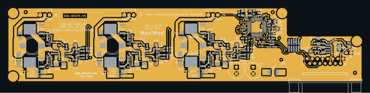
Design review
Probe recorded 18 findings: 8 major · 10 minor (25 items) on this design. Each is shown here with its reasoning; the full review links every one to the pins, nets and datasheet pages it rests on.
BZX84C5V1 went end-of-life (Obsolete)
Vendor (DigiKey) lifecycle for BZX84C5V1 (onsemi's listing) changed from "Active" to "Obsolete" since this board was reviewed. Placed as D1, D11, D3, D5, D7, D9. A sourcing/longevity risk; consider a replacement before production.
22-04-1031 went end-of-life (Discontinued at DigiKey)
Vendor (DigiKey) lifecycle for 22-04-1031 (Molex's listing) changed from "Active" to "Discontinued at DigiKey" since this board was reviewed. Placed as J1, J3, J4. A sourcing/longevity risk; consider a replacement before production.
- concernCON-002majorOpen
[eol:22-04-1031:Discontinued at DigiKey] 22-04-1031 lifecycle changed from "Active" to "Discontinued at DigiKey" since this board was reviewed: OHWR0074 R4 DIOT MONIMOD FANTRAY. A sourcing and longevity risk. Should this be replaced before the next build?
- concernCON-001majorOpen
[eol:BZX84C5V1:Obsolete] BZX84C5V1 lifecycle changed from "Active" to "Obsolete" since this board was reviewed: OHWR0074 R4 DIOT MONIMOD FANTRAY. A sourcing and longevity risk. Should this be replaced before the next build?
- ReferencePlaneDiscontinuitymajorOpen
5 nets change reference between GND and P3V3 at 7 vias, none with a reference that continues across (fastest: /T_adc1 at 100 ps 10-90 %, ASSUMED)
At 7 via(s), on 5 net(s), the signal leaves a layer referenced by one of GND and P3V3 for a layer referenced by the other, and no plane references both layers. Different nets: no via can carry the return across; only decoupling between the two planes near the via can. The capacitor carrying the return across was measured at each via, at the knee of the crossing net's edge against 50 ohm assumed: 7 with none. 7 of them at an ASSUMED edge (no edge on file for the net): state one (net_timing_state) and it is re-read. One decision covers the pair: whether GND and P3V3 are decoupled to each other near these vias. A via whose layers have more references than these two is a site of each pair it joins. None is partial: at every one, no reference continues across the via.
- '/T_adc1' at (246.12, -124.25), F.CU -> B.CU: GND on IN1.CU to P3V3 on IN2.CU; pure, no reference continues across; stitching none, 62.7 mm of track past the via on B.CU: At the 5 GHz knee of a 100 ps edge (100 ps 10-90 %, assumed: no edge is on file for the net) no capacitor carries the return; only the planes do. GND and P3V3 are not a thin pair (at most 0.2 mm), so their own capacitance does not carry the return. To serve it, change layers across the same plane, or move the signal to a layer referenced to ground. None.
- '/VI_adc3' at (244.54, -126.54), F.CU -> B.CU: GND on IN1.CU to P3V3 on IN2.CU; pure, no reference continues across; stitching none, 40.0 mm of track past the via on B.CU: At the 5 GHz knee of a 100 ps edge (100 ps 10-90 %, assumed: no edge is on file for the net) no capacitor carries the return; only the planes do. GND and P3V3 are not a thin pair (at most 0.2 mm), so their own capacitance does not carry the return. To serve it, change layers across the same plane, or move the signal to a layer referenced to ground. Measured for reference: C25 (100 nF 0603) 2.6 mm away: 0.58 nH in the 0.480 mm cavity + 0.51 nH ESL + 0.68 nH mounting (pad 0.10 nH + no via of the first net within 1 mm of its pad: the study's 0.6 nH per mm of 0.96 mm depth, ASSUMED): 55.4 ohm at the knee, 111 % of 50 ohm (assumed track impedance). None.
- '/V_adc2' at (243, -120.5), F.CU -> B.CU: GND on IN1.CU to P3V3 on IN2.CU; pure, no reference continues across; stitching none, 22.6 mm of track past the via on B.CU: At the 5 GHz knee of a 100 ps edge (100 ps 10-90 %, assumed: no edge is on file for the net) no capacitor carries the return; only the planes do. GND and P3V3 are not a thin pair (at most 0.2 mm), so their own capacitance does not carry the return. To serve it, change layers across the same plane, or move the signal to a layer referenced to ground. None.
- '/swdio' at (256.25, -132.5), F.CU -> B.CU: GND on IN1.CU to P3V3 on IN2.CU; pure, no reference continues across; stitching none, 11.8 mm of track past the via on B.CU: At the 5 GHz knee of a 100 ps edge (100 ps 10-90 %, assumed: no edge is on file for the net) no capacitor carries the return; only the planes do. GND and P3V3 are not a thin pair (at most 0.2 mm), so their own capacitance does not carry the return. To serve it, change layers across the same plane, or move the signal to a layer referenced to ground. None.
- '/swdio' at (267, -135), F.CU -> B.CU: GND on IN1.CU to P3V3 on IN2.CU; pure, no reference continues across; stitching none, 11.8 mm of track past the via on B.CU: At the 5 GHz knee of a 100 ps edge (100 ps 10-90 %, assumed: no edge is on file for the net) no capacitor carries the return; only the planes do. GND and P3V3 are not a thin pair (at most 0.2 mm), so their own capacitance does not carry the return. To serve it, change layers across the same plane, or move the signal to a layer referenced to ground. None.
- '/swclk' at (255.34, -133.25), F.CU -> B.CU: GND on IN1.CU to P3V3 on IN2.CU; pure, no reference continues across; stitching none, 9.9 mm of track past the via on B.CU: At the 5 GHz knee of a 100 ps edge (1 ns 10-90 %, assumed: no edge is on file for the net) no capacitor carries the return; only the planes do. GND and P3V3 are not a thin pair (at most 0.2 mm), so their own capacitance does not carry the return. To serve it, change layers across the same plane, or move the signal to a layer referenced to ground. None.
- '/swclk' at (264.75, -134.5), F.CU -> B.CU: GND on IN1.CU to P3V3 on IN2.CU; pure, no reference continues across; stitching none, 9.9 mm of track past the via on B.CU: At the 5 GHz knee of a 100 ps edge (1 ns 10-90 %, assumed: no edge is on file for the net) no capacitor carries the return; only the planes do. GND and P3V3 are not a thin pair (at most 0.2 mm), so their own capacitance does not carry the return. To serve it, change layers across the same plane, or move the signal to a layer referenced to ground. None.
Every site is a row of this finding's evidence, keyed by net, layers and position. GET /api/odb/boards/87/reference-planes?group=refchange%3AGND%7CP3V3 serves each with its own layer_image region; all of them lie in x 241..269, y -137..-118.5 mm (board frame, Y up).
The reference on each layer is the first plane the track meets leaving the via, anti-pads and the net's own copper skipped. Whether it matters depends on each signal's edge rate, which nothing on file states for these nets: a slow static line crosses a split harmlessly, a fast edge does not.
At refchange:GND|P3V3
- PartLifecyclemajorOpen
BZX84C5V1 on 6 placements (D1, D11, D3, D5, D7, D9): the distributor catalogue reports "Obsolete" for onsemi's BZX84C5V1
BZX84C5V1 on 6 placements (D1, D11, D3, D5, D7, D9): the distributor catalogue reports "Obsolete" for onsemi's BZX84C5V1 — a sourcing/longevity risk to confirm against the MANUFACTURER before acting. This board's BOM names FAIRCHILD SEMICONDUCTOR, and that is one line with onsemi: ON Semiconductor completed its acquisition of Fairchild Semiconductor on 2016-09-19 and renamed itself onsemi on 2021-08-05. A distributor delisting is not the same claim as the part being unavailable; check the vendor's own lifecycle/product-change notice for the status and any named successor. Re-read the source: GET /api/odb/parts/BZX84C5V1/providers (which provider said it, the maker and part number it matched, its own words, and when we asked). THE LAST BUY DATE HAS PASSED (2017-11-19, 3,283 day(s) ago), so this is a substitution rather than a buy. The distributor reports NONE left. No approved alternate is recorded for this position.
At D1
- PartLifecyclemajorOpen
PartLifecycle: 3 part numbers×3
2 Obsolete, 1 Not For New Designs · on 14 placements
At D10, F1, IC10
Each finding, with its own headline
D10BAT54C on 12 placements (D10, D12, D16, D17, D18, D19, D2, D20, …): the distributor catalogue reports "Obsolete" for onsemi's BAT54C
BAT54C on 12 placements (D10, D12, D16, D17, D18, D19, D2, D20, …): the distributor catalogue reports "Obsolete" for onsemi's BAT54C — a sourcing/longevity risk to confirm against the MANUFACTURER before acting. This board's BOM names FAIRCHILD SEMICONDUCTOR, and that is one line with onsemi: ON Semiconductor completed its acquisition of Fairchild Semiconductor on 2016-09-19 and renamed itself onsemi on 2021-08-05. A distributor delisting is not the same claim as the part being unavailable; check the vendor's own lifecycle/product-change notice for the status and any named successor. Re-read the source: GET /api/odb/parts/BAT54C/providers (which provider said it, the maker and part number it matched, its own words, and when we asked). THE LAST BUY DATE HAS PASSED (2018-09-30, 2,968 day(s) ago), so this is a substitution rather than a buy. The distributor reports 54,983 left. No approved alternate is recorded for this position.
F1MF-MSMF110/16-2 on F1: the distributor catalogue reports "Not For New Designs" for Bourns Inc.'s MF-MSMF110/16-2
MF-MSMF110/16-2 on F1: the distributor catalogue reports "Not For New Designs" for Bourns Inc.'s MF-MSMF110/16-2 — a sourcing/longevity risk to confirm against the MANUFACTURER before acting. That is the maker this board's BOM names (BOURNS). A distributor delisting is not the same claim as the part being unavailable; check the vendor's own lifecycle/product-change notice for the status and any named successor. Re-read the source: GET /api/odb/parts/MF-MSMF110/16-2/providers (which provider said it, the maker and part number it matched, its own words, and when we asked). No approved alternate is recorded for this position.
IC10LM45CIM3 on IC10: the distributor catalogue reports "Obsolete" for Texas Instruments's LM45CIM3
LM45CIM3 on IC10: the distributor catalogue reports "Obsolete" for Texas Instruments's LM45CIM3 — a sourcing/longevity risk to confirm against the MANUFACTURER before acting. That is the maker this board's BOM names (TEXAS INSTRUMENTS). A distributor delisting is not the same claim as the part being unavailable; check the vendor's own lifecycle/product-change notice for the status and any named successor. Re-read the source: GET /api/odb/parts/LM45CIM3/providers (which provider said it, the maker and part number it matched, its own words, and when we asked). No approved alternate is recorded for this position.
- ReferencePlaneDiscontinuitymajorOpen
ReferencePlaneDiscontinuity: 3 boards×3
Checked by the review, stands · Claude walker D (Cern session) — Checked: the nets crossing the GND/P3V3 split on IN2.CU, the reference changes and the B.CU/IN2.CU pour voids are slow board signals: fan tachometer inputs, fan PWM control at fan rates, I2C (scl/sda) and DC analog sense lines (VI_adc3). None is a fast edge; no edge is stated and nothing on file asks for controlled impedance on them. Left for the owner.
At split@IN2.CU:GND|P3V3, void:GND@IN2.CU:229.66,-128.29, void:routed@B.CU|IN2.CU
Each finding, with its own headline
split@IN2.CU:GND|P3V35 nets cross the split between the GND and P3V3 planes on IN2.CU at 15 places, with no plane on the track's other side (fastest: /T_adc1 at 100 ps 10-90 %, ASSUMED)
On IN2.CU the GND and P3V3 planes part, and 5 nets cross from one to the other at 15 place(s). The return current cannot follow a track across; it detours to wherever the two planes are joined (a stitching capacitor, or the source), and the loop it opens radiates and couples. One decision covers the boundary: whether it is stitched near these crossings, or the nets crossing it are slow enough not to care. Tracks that run ALONG this split, down the slot rather than across it, are a finding of their own: theirs is an impedance step, not a detour. At 0 of the 15 crossing(s) the track's other neighbour carries a plane, which the return can use there; 15 are on an outer layer, with no other neighbour. No crossing has a plane on the track's other side, so the whole return meets the break.
- '/T_adc1' on B.CU at (231.63, -128.86), 0.36 mm; other side: none: the signal layer is outermost
- '/T_adc1' on B.CU at (239.86, -128.69), 0.37 mm; other side: none: the signal layer is outermost
- '/T_adc1' on B.CU at (241.43, -127.12), 0.54 mm; other side: none: the signal layer is outermost
- '/VI_adc3' on B.CU at (232.78, -130.22), 0.42 mm; other side: none: the signal layer is outermost
- '/VI_adc3' on B.CU at (240.8, -128.69), 0.37 mm; other side: none: the signal layer is outermost
- '/VI_adc3' on B.CU at (241.37, -128.13), 0.37 mm; other side: none: the signal layer is outermost
- '/V_adc1' on B.CU at (243.72, -121.27), 0.26 mm; other side: none: the signal layer is outermost
- '/V_adc1' on B.CU at (245.38, -122.28), 0.37 mm; other side: none: the signal layer is outermost
- '/V_adc1' on B.CU at (245.5, -128.62), 0.31 mm; other side: none: the signal layer is outermost
- '/V_adc1' on B.CU at (248.3, -135.18), 0.37 mm; other side: none: the signal layer is outermost
- '/V_adc2' on B.CU at (245.38, -121.22), 0.37 mm; other side: none: the signal layer is outermost
- '/V_adc2' on B.CU at (246.25, -129.34), 0.36 mm; other side: none: the signal layer is outermost
- and 3 more
Every site is a row of this finding's evidence, keyed by net, layers and position. GET /api/odb/boards/87/reference-planes?group=split%40IN2.CU%3AGND%7CP3V3 serves each with its own layer_image region; all of them lie in x 230.5..252.02, y -136.31..-120.09 mm (board frame, Y up).
Read from the copper as drawn on the reference layer, along each track's centreline at exact breakpoints. The reference is the copper beside the track, never the layer's type or name. Whether it matters depends on each signal's edge rate, which nothing on file states for these nets: a slow static line crosses a split harmlessly, a fast edge does not.
void:GND@IN2.CU:229.66,-128.29'/VI_adc3' crosses where the outline of the GND plane on IN2.CU is drawn back, at 1 place, the longest 5.81 mm (fastest: /VI_adc3 at 100 ps 10-90 %, ASSUMED)
Along '/VI_adc3' on B.CU, the GND plane on IN2.CU has 5.81 mm under the track with no copper, at (229.66, -128.29), the same plane on both sides. No single drill's anti-pad and no landing explains it: a clearance is excused only when it holds a drill and is drawn round it, or the track ends in it on the net's own pad or via, or runs through its own via's clearance and no farther. The return current detours round the void. 1 of them run ALONG the bare copper, parallel to its edges, rather than across it (the longest 4.96 mm). No hole cleared it: the outline of the pour at x 107.5..296.5, y -149.5..-110.5 is drawn back there. One decision covers the void: whether these tracks may cross it, or the plane should be filled under them. No crossing has a plane on the track's other side, so the whole return meets the break.
- '/VI_adc3' on B.CU at (229.66, -128.29), 5.81 mm, running ALONG the bare copper for 4.96 mm, not across it over no copper; other side: none: the signal layer is outermost
Every site is a row of this finding's evidence, keyed by net, layers and position. GET /api/odb/boards/87/reference-planes?group=void%3AGND%40IN2.CU%3A229.66%2C-128.29 serves each with its own layer_image region; all of them lie in x 226.72..232.93, y -131.22..-125.35 mm (board frame, Y up).
Read from the copper as drawn on the reference layer, along each track's centreline at exact breakpoints. The reference is the copper beside the track, never the layer's type or name. Whether it matters depends on each signal's edge rate, which nothing on file states for these nets: a slow static line crosses a split harmlessly, a fast edge does not.
void:routed@B.CU|IN2.CUTracks on B.CU and IN2.CU cross each other at 6 places, each layer the other's reference with its pour cleared round its own tracks, the longest 3.25 mm; 1 runs ALONG the cut round another net's track (fastest: /Fan_ctrl_h1 at 100 ps 10-90 %, ASSUMED)
B.CU and IN2.CU each carry a pour and routed tracks, and each is the other's nearest reference. Wherever a track on one crosses a track on the other, the pour under it is cleared round that other track, so for the width of the cut the return has no plane under it and detours round the cut. 6 place(s) on 8 net(s), 1 of them seen from both tracks (each counted once). 1 of the crossings run ALONG the cut round another net's track rather than across it, parallel to its edges (the longest 1.41 mm): over or right beside that track, broadside to it as well as off the plane. One decision covers the layer pair: whether these layers may take a pour their own tracks cut as the reference, or the routing or the stackup should give the tracks a plane that is not cut where they cross. 5 of the 9 crossing(s) have a plane on the track's other side at most twice as far away as the broken one (to first order each plane beside a stripline carries a share of the return inversely proportional to its distance from the track). The rest leave most or all of the return to the break, so the finding is a warning.
- one crossing of two tracks, seen from each: '/Fan_ctrl_h1' on IN2.CU at (180.37, -121.27), 3.25 mm over copper of /VI_adc2, /VI_adc1, not a plane; other side: GND on IN1.CU, 0.48 mm from the track against 0.48 mm to B.CU: 50% of the return on B.CU / '/Fan_ctrl_l1' on IN2.CU at (181.02, -120.62), 3.25 mm over copper of /VI_adc1, /VI_adc2, not a plane; other side: GND on IN1.CU, 0.48 mm from the track against 0.48 mm to B.CU: 50% of the return on B.CU / '/VI_adc1' on B.CU at (179.97, -120.95), 1.99 mm over copper of /Fan_ctrl_h1, /Fan_ctrl_l1, not a plane; other side: none: the signal layer is outermost / '/VI_adc2' on B.CU at (181.43, -120.95), 1.99 mm over copper of /Fan_ctrl_l1, /Fan_ctrl_h1, not a plane; other side: none: the signal layer is outermost
- 'Net-(IC7A-IN+)' on B.CU at (249.75, -137.84), 1.04 mm over copper of +5VA, not a plane; other side: none: the signal layer is outermost
- '/VI_adc3' on B.CU at (214.24, -126.26), 1.01 mm over copper of +5VA, not a plane; other side: none: the signal layer is outermost
- '/scl' on IN2.CU at (282.49, -136.76), 3.02 mm over copper of P5V, not a plane; other side: GND on IN1.CU, 0.48 mm from the track against 0.48 mm to B.CU: 50% of the return on B.CU
- '/scl' on IN2.CU at (265.58, -127.23), 2.52 mm, running ALONG the bare copper for 1.41 mm, not across it over copper of P3V3, not a plane; other side: GND on IN1.CU, 0.48 mm from the track against 0.48 mm to B.CU: 50% of the return on B.CU
- '/sda' on IN2.CU at (264.7, -127.81), 2.16 mm over copper of P3V3, not a plane; other side: GND on IN1.CU, 0.48 mm from the track against 0.48 mm to B.CU: 50% of the return on B.CU
Every site is a row of this finding's evidence, keyed by net, layers and position. GET /api/odb/boards/87/reference-planes?group=void%3Arouted%40B.CU%7CIN2.CU serves each with its own layer_image region; all of them lie in x 177.75..283.49, y -139.34..-119.24 mm (board frame, Y up).
Read from the copper as drawn on the reference layer, along each track's centreline at exact breakpoints. The reference is the copper beside the track, never the layer's type or name. Whether it matters depends on each signal's edge rate, which nothing on file states for these nets: a slow static line crosses a split harmlessly, a fast edge does not.
No fiducials on either side, with 114 SMT parts on top (including a 0.5 mm-pitch QFP) and 26 on the bottom
OHWR0074 R1 DIOT MONIMOD FANTRAY carries no fiducial on either side: no FTG/FID component, no fiducial pad, while the top holds 114 SMT placements including IC4, the 48-pin 0.5 mm-pitch SAMD21 QFP, and the bottom 26. Its sibling OHWR0073 DIOT MONIMOD has three top-side fiducials (FTG1-FTG3). A panel may carry global fiducials, but nothing in the board data provides them.
Side SMT placements Fiducials Source Top 114 0 ODB++ placement, layer view Bottom 26 0 ODB++ placement ADC reference IC5 (TL431) runs at 0.40 mA, below its 1 mA minimum, with 100 nF on its cathode inside the TL431 oscillation band
Vref25, the SAMD21's ADC reference (IC4 pin 4, PA03/VREFA), comes from IC5 TL431B biased by R10 = 2 k from P3V3_AUX: (3.3 - 2.495) / 2 k = 0.40 mA, below the 1 mA minimum recommended cathode current, with C19 = 100 nF directly on the cathode inside the TL431's low-current oscillation band. The same circuit was raised on OHWR0074 R1 (OBS-501) and is unchanged in this EDMS V4 release.
Quantity Value Source Bias resistor R10 2 k, P3V3_AUX to Vref25 netlist; schematic sheet 5 'ADC voltage reference' Cathode current available (3.3 - 2.495) / 2000 = 0.40 mA, less the VREFA input computed Recommended cathode current 1 mA min TL431 datasheet Table 8, p.6 I_K(min), TL431B 0.4 typ, 0.6 max mA TL431 datasheet Table 10, p.8 Load capacitance C19 100 nF on Vref25 netlist / BOM Oscillation band at low I_K Fig. 17, p.12 (typical) TL431 datasheet Why it matters
The reference sets the scale of every ADC reading on the board (fan currents VI_adc1-3, rail voltages V_adc1-2, temperature T_adc1). Biased at the bottom of its range and loaded by a capacitor in its oscillation band, its voltage and stability are not specified. A bias of about 1-2 mA (R10 about 470 R to 820 R) and a capacitor outside the band would put it back in its rated operating range.
Fan Tray cable shield bonds chassis PE (Front Interface J5 shell) to the fan tray's logic GND (J5 shell = GND): confirm the grounding is intended
The shielded Fan Tray cable joins chassis PE to the fan tray's logic GND: the DI/OT Crate spec asks for the shield to be bonded to the metal shell of both DSUB15s, and on this board J5's shell (pins 16, 17) is GND, while on the crate side (OHWR0086 R5 DIOT CRATE FRONT INTERFACE J5) the shell is PE. Please confirm this grounding is intended.
The path
``
mermaid graph LR PE["Front Interface PE (J5 shell, M1/M2)"] -- "cable shield" --> SH["Fan tray J5 shell (pins 16, 17)"] SH --> GND["Fan tray GND"] GND -- "cable pins 1,3,5,7,15" --> CGND["Crate logic GND"]``Point Net Source Fan tray J5.16 / J5.17 (DSUB shell) GND this board's netlist; schematic sheet 3 'front panel connector' Fan tray mounting holes B1-B4 unconnected this board's netlist Front Interface J5.16 / J5.17 (upper DSUB shell), M1, M2 PE OHWR0086 R5 netlist Front Interface B1 (banana socket) 1 M (R1) to PE OHWR0086 R5 netlist and BOM Cable DSUB15 1:1, shield to both shells DI/OT Crate specification v3.1 sec.5.2, p.12 Why ask
With the shield bonded at both ends, chassis PE and logic GND are tied at the fan tray, through the shell, while the crate otherwise separates them (the Front Interface ties its banana socket to PE only through 1 M). That makes the fan tray the place where PE and GND meet: a second return for fan and ESD currents and a ground loop with the crate's own GND, or a deliberate single bond. Nothing on the drawings says which. If PE is meant to stay off logic GND, bonding the fan tray shell to chassis rather than to GND (or the shield at one end only) would keep them apart; if it is meant, a note on the drawing would record it.
With shdn_n (crate F_RST) low the SAMD21 is unpowered while IC7/IC9 keep driving about 2 V into its ADC pins, above VDD + 0.6 V
When the crate holds the fan tray off (shdn_n low), P3V3 and the SAMD21 (IC4) are unpowered but P12V and P5V stay up, so the op-amp buffers keep driving about 2 V into the unpowered MCU's analog pins - above its VDD + 0.6 V absolute maximum.
The supplies are switched apart
``
mermaid graph LR P5V --> IC6["IC6 TPS7A4533 (SHDN = shdn_n)"] --> P3V3["P3V3 / P3V3_AUX: SAMD21 VDDIO, VDDANA"] P5V --> L5 --> A5["+5VA: IC7, IC10 LM45"] P12V --> OPS["IC8, IC9 supplies"] A5 --> IC7["IC7 buffers"] -->|"V_adc1, V_adc2"| MCU["IC4 PB08, PB09"] OPS --> IC9A["IC9A x2 (LM45)"] -->|"T_adc1"| MCU2["IC4 PA02"]``Quantity Value Source shdn_n J5 pin 9 from the crate (Front Interface J5 U9 = F_RST), 10 k up to P5V, 16 k down netlist; schematic sheets 2, 3 IC6 off SHDN below 0.25-0.75 V turns the 3.3 V LDO off TPS7A45xx datasheet p.6 IC7 supply +5VA (P5V through L5), not switched by shdn_n netlist V_adc1 P12V x 2 k / (10 k + 2 k) = 2.0 V, buffered by IC7A into IC4 pin 8 (PB09) netlist R15/R16 V_adc2 +5VA x 10 k / (16 k + 10 k) = 1.9 V, buffered by IC7B into IC4 pin 7 (PB08) netlist R20/R22 T_adc1 2 x LM45 output (10 mV/C), IC9A on P12V into IC4 pin 3 (PA02) netlist R25/R29 SAMD21 pin limit GND - 0.6 V to VDD + 0.6 V SAM D21 datasheet sec.37.3, p.864 Why it matters
With VDD at 0 V the pins accept 0.6 V at most, and they see about 2 V from a low-impedance op-amp output with no series resistor. The current flows through the input protection into the unpowered VDD and VDDANA, back-powering the MCU and the P3V3 rail through its ESD structure, every time the system board holds F_RST asserted with the crate supplies on. A series resistor at each ADC input (limiting the injection), or supplying the buffers from the switched 3.3 V domain, would remove it. Please confirm whether F_RST is ever held low with 12 V and 5 V present.
With F_RST holding the fan tray off, the crate's 3.3 V management I2C and the SWD lines from the system board back-feed the unpowered SAMD21 through J5
When the system board holds F_RST (this board's shdn_n) low, IC6 turns this board's P3V3 off and the SAMD21 (IC4) is unpowered. The crate still pulls the management I2C to 3.3 V on the system board, and the system board's FPGA can still drive the SWD lines, and all four reach IC4's pins directly through the 1:1 fan tray cable. The unpowered SAMD21 is then fed through its pins, above its VDD + 0.6 V limit, and its input protection loads the management bus that the PSU monitors share.
[OBS-586] covers the same shutdown state from this board's own op-amps. This one is the crate side of it.
The path (OHWR-DIOT-CRATE-V3, both builds)
``
mermaid graph LR SB["SB ZU R5: M_SCL/M_SDA pulled to 3.3 V (R329, R368 4k7, IC42 LTC4311); F_IO0/F_IO1 from IC52 bank 94 (3.3 V)"] --> BP["Main backplane"] --> FI["Front Interface J5 upper"] -->|"fan tray cable 1:1"| J5["this board J5 10, 12, 13, 14"] J5 --> MCU["IC4 SAMD21: SCL 14, SDA 13, SWCLK 45, SWDIO 46 (VDD = P3V3, off)"] F["F_RST = shdn_n (J5.9)"] --> LDO["IC6 TPS7A4533 SHDN"] -->|off| P3["P3V3"]``The numbers
Quantity Value Source shdn_n J5.9, crate F_RST (spec Table 5); R14 10 k to P5V, R41 16 k to GND; IC6 SHDN this board's netlist SAMD21 supply P3V3, the output of IC6, off while shdn_n is low netlist (IC4 pins 17, 36, 44) Pins reached from the crate IC4.14 /scl, IC4.13 /sda (no series resistor); IC4.45 /swclk, IC4.46 /swdio (R12, R39 10 k to P3V3) netlist; cable J5 10, 12, 13, 14 Bus high level 3.3 V from the system board's P3V3 (4.7 k pull-ups plus the LTC4311 accelerator) OHWR0083 R5 netlist SAMD21 pin limit GND − 0.6 V to VDD + 0.6 V SAM D21 datasheet, Table 37-2, p.864 Why it matters
- With VDD at 0 V each of these pins tolerates 0.6 V and sees 3.3 V. The pull-up and accelerator current flows through the input protection into the switched-off P3V3, back-powering the MCU.
- The management bus is shared with the AD7291 monitors on both PSUs. While the fan tray is held off, its clamped pins can keep the bus from reaching a valid high level, so the PSU telemetry can stop exactly while the fan tray is being reset.
- The reverse also exists at crate power-up: this board's P5V comes straight from the crate, so the shdn_n divider (about 3.1 V through about 6.2 kΩ) and R12/R39 (to this board's P3V3) present a high level to the system board's FPGA pins (IC52 F6, E2, E3) before the system board's own 3.3 V is up.
Powering IC4 from a rail that shdn_n does not switch, or an I2C buffer and series resistors on the J5 signals, would keep the two domains apart.
Fan half-bridges have no guaranteed dead time: LIN is driven as the exact complement of HIN (firmware), through identical RC filters
The three fan half-bridges (IC1/IC2/IC3 NCP5183 driving T1–T6) get no guaranteed dead time: the firmware drives LIN as the exact complement of HIN, and whether the high- and low-side MOSFETs overlap at each edge depends on where the NCP5183's input thresholds happen to fall.
How the inputs are generated
The MoniMod firmware (OHWR diot-monimod
main_fw, git 4e7c8230 of 2025-04-10,atmel_start_prj/hpl/tc/hpl_tc.c) patches the SAMD21 TC driver for a *complementary* output: NPWM mode,INVEN0set, and the same compare value written to CC0 and CC1 (_pwm_set_param, "intentionally using cc1"). PER = 255 at an 8 MHz GCLK gives about 31.25 kHz. So each TC's WO0 is the logic inverse of WO1, with no dead-time insertion (the plain TC has none; the TCC's dead-time generator is not used).Fan HIN (pin 1) LIN (pin 2) Driver High side / low side 1 IC4 pin 28 PA19 = TC3 WO1 IC4 pin 27 PA18 = TC3 WO0 IC1 T1 / T2 2 IC4 pin 32 PA23 = TC4 WO1 IC4 pin 31 PA22 = TC4 WO0 IC2 T3 / T4 3 IC4 pin 20 PB11 = TC5 WO1 IC4 pin 19 PB10 = TC5 WO0 IC3 T5 / T6 Why the hardware does not add it
Both inputs pass through identical 1 kΩ / 1 nF filters (τ = 1 µs; R8/C40 and R30/C41 on fan 1, and so on), so both edges slew alike. The NCP5183 has no shoot-through interlock: its two channels are independent, and the datasheet guarantees only VIH ≤ 2.5 V and VIL ≥ 1.2 V (p.4), with delay matching of 0–50 ns. From 3.3 V logic through τ = 1 µs, the turning-on channel crosses its threshold at τ·ln(3.3/(3.3 − V_on)) and the turning-off channel at τ·ln(3.3/V_off). The two MOSFETs conduct together whenever V_on + V_off < 3.3 V, which those limits do not exclude.
What an overlap costs
``
mermaid graph LR P12V -->|R13 0.05 Ω| IFAN[/I_fan1/] IFAN -->|T1 high side| OUT[fan_driver_1/OUT] OUT -->|T2 low side| GND``Quantity Value Source Supply 12 V rail P12V Sense resistor 0.05 Ω R13 (BOM) RDS(on) per MOSFET 0.43 Ω max at VGS 10 V IPD5N25S3-430 datasheet p.2 Shoot-through current ≈ 12 V / 0.91 Ω ≈ 13 A for the overlap derived This would recur on every PWM edge, 2 × 31.25 kHz per fan. Whether it happens on a given unit depends on threshold placement the datasheet does not specify, so CERN is asked to confirm: either a dead time is intended elsewhere (the TCC dead-time generator, firmware edge offsets), or the margin was measured on hardware.
1 clock net (SWD clock /swclk) changes reference between GND and P3V3 at 2 vias with no return path
The SWD clock /swclk, which the crate's system board drives into the fan tray through the Fan Tray cable (J5.13) and the bench header J2.4, changes reference between the GND plane (IN1.CU) and the P3V3 plane (IN2.CU) at two vias with no stitching capacitor near either: its return current has no continuous path there.
Read from the copper as drawn (Probe's reference-plane screen on this take). No edge rate is on file for this net (the driver is the system board or the bench programmer, off this board), so no noise figure is claimed; the geometry is exact.
Sites
Net Kind Via (mm) Layers Reference before / after Track past the via Stitching /swclk SWD clock (IC4.45 SAMD21 PA30, J2.4, J5.13, pull R12) (255.34, -133.25) F.CU to B.CU GND on IN1.CU to P3V3 on IN2.CU 9.9 mm on B.CU none near the via /swclk (same net) (264.75, -134.50) F.CU to B.CU GND on IN1.CU to P3V3 on IN2.CU 9.9 mm on B.CU none near the via Why it is raised
It is the only clock on this board that changes reference without a path for its return; the other crossings on the board (fan PWM and tacho, I2C, DC analog sense, reset) are slow or static and were checked as layout practice. The SWD clock arrives over a cable from another board, so a poor return here adds to what the cable carries. A ground via beside each signal via, or routing the B.CU stretch over a GND reference, removes it.
Fan-tray input fuse F1 is two different parts: drawn and valued MF-MSMF150/12 (3 A trip, 12 V max), ordered as MF-MSMF110/16 (1.1 A hold, 16 V max)
The PTC fuse F1 that protects the crate's 12 V input (J5 pins 2/4/6/8 to P12V) is a different part depending on where you read it. The schematic labels it "3A-12V" and the BOM row's value is FUSR_BOURNS_MF-MSMF150/12-2, but the same row orders MF-MSMF110/16-2 (comment "1.1A-16V"). The two differ in hold current and in maximum voltage, and the 12 V variant would sit at its own voltage limit on this 12 V rail.
The two candidates
Part V max I hold I trip Source MF-MSMF150/12 (schematic "3A-12V", BOM value) 12 V 1.50 A 3.00 A Bourns MF-MSMF datasheet p2 MF-MSMF110/16 (BOM MPN, comment "1.1A-16V") 16 V 1.10 A 2.20 A Bourns MF-MSMF datasheet p1 Rail it protects 12.0 V nominal (P12V, fans and gate drivers) netlist Why it matters
Whichever is fitted sets how much fan current the tray carries before tripping (1.1 A versus 1.5 A hold), and the 150/12 variant's 12 V maximum leaves no margin over a 12 V supply with any tolerance on it. The board should name one part, and the label, value and MPN should agree.
- ConnectorDomainMixedminorOpen
J5 takes 2 different supplies off the board on one connector: Net-(F1-Pad2) (12.0 V), P5V (5.0 V)
J5 carries 2 different supplies out of the board on one connector: Net-(F1-Pad2) (12.0 V) on 2/4/6/8, P5V (5.0 V) on 11. Declare the intent. Two rails on one connector is ordinary in a docking or power-distribution interface and a hazard in a signal one, and the difference is not visible from the netlist — but note that adjacent contacts at different voltages are exactly what a mirrored, reversed or off-by-one cable shorts together, so the cost of getting the mating wrong is a rail collision rather than a dead signal. If this is a standard connector, declare its family (connector_family_declare) and file the standard's contact map: supplies on the contacts it assigns to power are then not reported.
At J5
- ReferencePlaneDiscontinuityminorOpen
ReferencePlaneDiscontinuity: 4 boards×4
Checked by the review, stands · Claude walker D (Cern session) — Checked: the nets crossing the GND/P3V3 split on IN2.CU, the reference changes and the B.CU/IN2.CU pour voids are slow board signals: fan tachometer inputs, fan PWM control at fan rates, I2C (scl/sda) and DC analog sense lines (VI_adc3). None is a fast edge; no edge is stated and nothing on file asks for controlled impedance on them. Left for the owner.
At void:GND@B.CU:206.76,-116.31, void:GND@B.CU:212.25,-122.73, void:GND@B.CU:266.89,-127.23, void:GND@B.CU:277.01,-137.46
Each finding, with its own headline
void:GND@B.CU:206.76,-116.31'/Fan_tacho1' crosses where the outline of the GND plane on B.CU is drawn back, at 1 place, the longest 46.06 mm (fastest: /Fan_tacho1 at 100 ps 10-90 %, ASSUMED)
Along '/Fan_tacho1' on IN2.CU, the GND plane on B.CU has 46.06 mm under the track with no copper, at (206.76, -116.31), the same plane on both sides. No single drill's anti-pad and no landing explains it: a clearance is excused only when it holds a drill and is drawn round it, or the track ends in it on the net's own pad or via, or runs through its own via's clearance and no farther. The return current detours round the void. 1 of them run ALONG the bare copper, parallel to its edges, rather than across it (the longest 45.54 mm). No hole cleared it: the outline of the pour at x 107.5..296.5, y -149.5..-110.5 is drawn back there. One decision covers the void: whether these tracks may cross it, or the plane should be filled under them. Every crossing has a plane on the track's other side at most twice as far away as the broken one, so at most 50% of the return meets the break and the rest follows the track on that plane (to first order each plane beside a stripline carries a share of the return inversely proportional to its distance from the track). The finding is the lower tier (info).
- '/Fan_tacho1' on IN2.CU at (206.76, -116.31), 46.06 mm, running ALONG the bare copper for 45.54 mm, not across it over no copper; other side: GND on IN1.CU, 0.48 mm from the track against 0.48 mm to B.CU: 50% of the return on B.CU
Every site is a row of this finding's evidence, keyed by net, layers and position. GET /api/odb/boards/87/reference-planes?group=void%3AGND%40B.CU%3A206.76%2C-116.31 serves each with its own layer_image region; all of them lie in x 182.73..230.79, y -117.31..-115.31 mm (board frame, Y up).
Read from the copper as drawn on the reference layer, along each track's centreline at exact breakpoints. The reference is the copper beside the track, never the layer's type or name. Whether it matters depends on each signal's edge rate, which nothing on file states for these nets: a slow static line crosses a split harmlessly, a fast edge does not.
void:GND@B.CU:212.25,-122.73'/Fan_ctrl_h2' crosses where the outline of the GND plane on B.CU is drawn back, at 1 place, the longest 0.29 mm (fastest: /Fan_ctrl_h2 at 100 ps 10-90 %, ASSUMED)
Along '/Fan_ctrl_h2' on IN2.CU, the GND plane on B.CU has 0.29 mm under the track with no copper, at (212.25, -122.73), the same plane on both sides. No single drill's anti-pad and no landing explains it: a clearance is excused only when it holds a drill and is drawn round it, or the track ends in it on the net's own pad or via, or runs through its own via's clearance and no farther. The return current detours round the void. No hole cleared it: the outline of the pour at x 107.5..296.5, y -149.5..-110.5 is drawn back there. One decision covers the void: whether these tracks may cross it, or the plane should be filled under them. Every crossing has a plane on the track's other side at most twice as far away as the broken one, so at most 50% of the return meets the break and the rest follows the track on that plane (to first order each plane beside a stripline carries a share of the return inversely proportional to its distance from the track). The finding is the lower tier (info).
- '/Fan_ctrl_h2' on IN2.CU at (212.25, -122.73), 0.29 mm over no copper; other side: GND on IN1.CU, 0.48 mm from the track against 0.48 mm to B.CU: 50% of the return on B.CU
Every site is a row of this finding's evidence, keyed by net, layers and position. GET /api/odb/boards/87/reference-planes?group=void%3AGND%40B.CU%3A212.25%2C-122.73 serves each with its own layer_image region; all of them lie in x 211.09..213.35, y -123.73..-121.66 mm (board frame, Y up).
Read from the copper as drawn on the reference layer, along each track's centreline at exact breakpoints. The reference is the copper beside the track, never the layer's type or name. Whether it matters depends on each signal's edge rate, which nothing on file states for these nets: a slow static line crosses a split harmlessly, a fast edge does not.
void:GND@B.CU:266.89,-127.23'/scl' crosses where the outline of the GND plane on B.CU is drawn back, at 1 place, the longest 0.69 mm (fastest: /scl at 10 ns 10-90 %, suggested by its name)
Along '/scl' on IN2.CU, the GND plane on B.CU has 0.69 mm under the track with no copper, at (266.89, -127.23), the same plane on both sides. No single drill's anti-pad and no landing explains it: a clearance is excused only when it holds a drill and is drawn round it, or the track ends in it on the net's own pad or via, or runs through its own via's clearance and no farther. The return current detours round the void. 1 of them run ALONG the bare copper, parallel to its edges, rather than across it (the longest 0.69 mm). No hole cleared it: the outline of the pour at x 107.5..296.5, y -149.5..-110.5 is drawn back there. One decision covers the void: whether these tracks may cross it, or the plane should be filled under them. Every crossing has a plane on the track's other side at most twice as far away as the broken one, so at most 50% of the return meets the break and the rest follows the track on that plane (to first order each plane beside a stripline carries a share of the return inversely proportional to its distance from the track). The finding is the lower tier (info).
- '/scl' on IN2.CU at (266.89, -127.23), 0.69 mm, running ALONG the bare copper for 0.69 mm, not across it over no copper; other side: GND on IN1.CU, 0.48 mm from the track against 0.48 mm to B.CU: 50% of the return on B.CU
Every site is a row of this finding's evidence, keyed by net, layers and position. GET /api/odb/boards/87/reference-planes?group=void%3AGND%40B.CU%3A266.89%2C-127.23 serves each with its own layer_image region; all of them lie in x 265.55..268.24, y -128.23..-126.23 mm (board frame, Y up).
Read from the copper as drawn on the reference layer, along each track's centreline at exact breakpoints. The reference is the copper beside the track, never the layer's type or name. Whether it matters depends on each signal's edge rate, which nothing on file states for these nets: a slow static line crosses a split harmlessly, a fast edge does not.
void:GND@B.CU:277.01,-137.46'/sda' crosses where the outline of the GND plane on B.CU is drawn back, at 1 place, the longest 0.6 mm (fastest: /sda at 10 ns 10-90 %, suggested by its name)
Along '/sda' on IN2.CU, the GND plane on B.CU has 0.6 mm under the track with no copper, at (277.01, -137.46), the same plane on both sides. No single drill's anti-pad and no landing explains it: a clearance is excused only when it holds a drill and is drawn round it, or the track ends in it on the net's own pad or via, or runs through its own via's clearance and no farther. The return current detours round the void. No hole cleared it: the outline of the pour at x 107.5..296.5, y -149.5..-110.5 is drawn back there. One decision covers the void: whether these tracks may cross it, or the plane should be filled under them. Every crossing has a plane on the track's other side at most twice as far away as the broken one, so at most 50% of the return meets the break and the rest follows the track on that plane (to first order each plane beside a stripline carries a share of the return inversely proportional to its distance from the track). The finding is the lower tier (info).
- '/sda' on IN2.CU at (277.01, -137.46), 0.6 mm over no copper; other side: GND on IN1.CU, 0.48 mm from the track against 0.48 mm to B.CU: 50% of the return on B.CU
Every site is a row of this finding's evidence, keyed by net, layers and position. GET /api/odb/boards/87/reference-planes?group=void%3AGND%40B.CU%3A277.01%2C-137.46 serves each with its own layer_image region; all of them lie in x 276.01..278.01, y -138.76..-136.16 mm (board frame, Y up).
Read from the copper as drawn on the reference layer, along each track's centreline at exact breakpoints. The reference is the copper beside the track, never the layer's type or name. Whether it matters depends on each signal's edge rate, which nothing on file states for these nets: a slow static line crosses a split harmlessly, a fast edge does not.
Main parts
| Part number | Maker | Description | Where |
|---|---|---|---|
| ABM3B-8.000MHZ-B2-T | ABRACON | Q1 | |
| ATSAMD21G18A-AF | MICROCHIP | IC4 | |
| BLM18PG121SN1D | MURATA | SMD EMIFIL Chip Ferrite Bead | L5 |
| BLM18SG221TN1 | MURATA | SMD EMIFIL Suppression Chip Ferrite Bead | L4 |
| FTS-105-01-F-DV | SAMTEC | 10 Contacts, Pitch 1.27mm, Dual Row Surface Mount Straight Strip Header | J2 |
| HTSW-101-23-L-D | SAMTEC | 2 Contacts, Pitch 2.54mm, Dual Row Through Mount Straight Header (Post Lead 5.84mm, Tail Lead 2.92mm, Insulator 2.54mm) | J6 |
| L717DFA15S1ATN | AMPHENOL | Right Angled D-Sub 15 Female Contacts with Metal Bracket and Front Female Screwlock (UNC4-40) | J5 |
| LM45CIM3 | TEXAS INSTRUMENTS | -20° to +100°C ±3°C Precision Centigrade Temperature Sensors | IC10 |
| MF-MSMF110/16-2 | BOURNS | F1 | |
| TL431BQDBZ | NXP SEMICONDUCTORS | Vref (2.495V) To 36V 0.5% Precision Programmable Reference | IC5 |
| TPS7A4533DCQ | TEXAS INSTRUMENTS | 3.3V Low-Noise Fast-Transient-Response 1.5A Low-Dropout Voltage Regulator | IC6 |
| BN5687 Art.3061605 | BOSSARD | M3 L=6mm Hexalobular Socket Pan Head Screw, Fully Threaded, Stainless Steel A2 | SCREW1, SCREW2 |
| BN628 Art.1241443 | BOSSARD | M3 Hexagon Nut ~0,8d, ISO 4032, DIN 934, Stainless Steel A2 | NUT1, NUT2 |
| BN83728 Art.8243964 | BOSSARD | Waved Spring Washer for M3 Screw - Steel 440-520 HV - Zinc Plated Blue | WASHER1, WASHER2 |
| CC0603_22PF_50V_5%_NP0 | GENERIC | SMD Multilayer Chip Ceramic Capacitor | C20, C21 |
| EEUFR1E221 | PANASONIC | Radial Miniature, Aluminum Electrolytic Capacitor, (FR-A Series) | C33, C34 |
| R0603_16K_1%_0.1W_100PPM | GENERIC | General Purpose Thick Film Chip Resistor | R20, R41 |
| 22-04-1031 | MOLEX | 2.5mm (.100") Pitch KK® Wire-to-Board Header, Vertical, with Friction Lock, 3 Circuits, Tin (Sn) Plating | J1, J3, J4 |
| BC817-25 | NXP SEMICONDUCTORS | 45V 500mA NPN General-Purpose Transistor | T7, T8, T9 |
| CC0603_1UF_16V_10%_X7R | GENERIC | SMD Multilayer Chip Ceramic Capacitor | C23, C24, C30 |
| CTE6032-28_22UF_25V_10%_LESR0250 | GENERIC | Low ESR 0R25 Solid Tantalum Chip Capacitor | C15, C3, C9 |
| DO3316P-473ML | COILCRAFT | L10, L6, L8 | |
| ES1D | FAIRCHILD SEMICONDUCTOR | Fast Rectifier | D13, D14, D15 |
| NCP5183DR2 | ON SEMICONDUCTOR | High Voltage High Current (4.3A), High and Low Side Driver | IC1, IC2, IC3 |
| OPA2192ID | TEXAS INSTRUMENTS | Dual 36V, Precision, Rail-to-Rail Input/Output, Low Offset Voltage, Low Input Bias Current Operational Amplifier with e-trim™ | IC7, IC8, IC9 |
| PLATED_HOLE3.2_PAD5.5 | Plated Through Hole: Hole Dia.=3.2mm Pad Dia.=5.5mm | B1, B2, B3, B4 | |
| R0603_2K_1%_0.1W_100PPM | GENERIC | General Purpose Thick Film Chip Resistor | R10, R16, R19, R24, R28 |
| BZX84C5V1 | FAIRCHILD SEMICONDUCTOR | D1, D11, D3, D5, D7, D9 | |
| CC0603_1NF_50V_10%_X7R | GENERIC | C40, C41, C42, C43, C44, C45 | |
| FIDUCIAL_TARGET_C100-200 | FTG1, FTG2, FTG3, FTG4, FTG5, FTG6 | ||
| IPD5N25S3-430 | INFINEON | 250V, 5A, N-Channel OptiMOS Power-Transistor | T1, T2, T3, T4, T5, T6 |
| R0603_1K_1%_0.1W_100PPM | GENERIC | General Purpose Thick Film Chip Resistor | R11, R30, R33, R34, R37, R38, R8 |
| GMJ316BB7106KLHT | TAIYO YUDEN | Soft Termination SMD Multilayer Chip Ceramic Capacitor for Automotive / Industrial Applications | C1, C10, C13, C16, C29, C31 and 3 more |
| SMD_PAD_1.27X1.27MM | 1.27mm x 1.27mm PCB Copper Area (SMD Test Point) | TP1, TP2, TP3, TP4, TP5, TP6 and 3 more | |
| BAT54C | FAIRCHILD SEMICONDUCTOR | Dual Common Cathode Small Signal Schottky Diode | D10, D12, D16, D17, D18, D19 and 6 more |
| R0603_10R_1%_0.1W_200PPM | GENERIC | General Purpose Thick Film Chip Resistor | R1, R2, R3, R31, R32, R35 and 6 more |
| CC0603_100NF_50V_10%_X7R | GENERIC | SMD Multilayer Chip Ceramic Capacitor | C11, C12, C14, C17, C18, C19 and 12 more |
| R0805_0R05_1%_0.25W_300PPM | GENERIC | Low Resistance Thick Film Chip Resistor | R13, R40, R42 |
| R0603_200R_1%_0.1W_100PPM | GENERIC | General Purpose Thick Film Chip Resistor | R17, R18, R21, R23, R26, R27 |
| R0603_10K_1%_0.1W_100PPM | GENERIC | General Purpose Thick Film Chip Resistor | R12, R14, R15, R22, R25, R29, R39 |
About this design
- Design
- DIOT MONIMOD FANTRAY — OHWR0074 R4
- Designed in
- KiCad EDA
- Board
- 4 copper layers, 190 × 40 mm, 158 components, 112 nets
- Licence
- CERN-OHL-W-2.0
- Source
- https://edms.cern.ch/item/EDA-04474-V4-0/0 at commit
EDMS EDA-044 - Attribution
- CERN EDMS item EDA-04474-V4-0 'DI/OT Fan-Tray Monimod': document 3220239 v.1, retrieved 2026-10-18T13:12:31Z. CERN EDA-04474 V4, DI/OT Fan-Tray Monimod. Copyright CERN 2021-2023, 2025. Licence: CERN OHL-W v2.0+. Source location: https://ohwr.org/project/diot-monimod
- Reviewed with
- Probe by E# (E-Sharp AB)