 Probe

DIOT SB ZU
OHWR0083 · revision R3 · a newer revision, R5, is listed
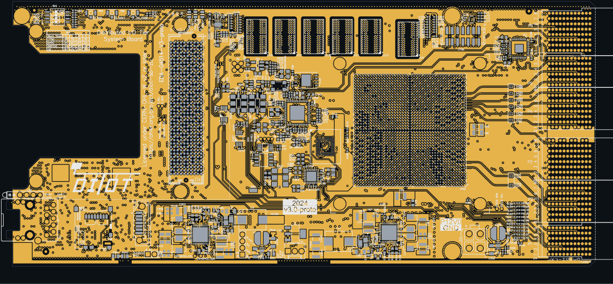
DIOT SB ZU (OHWR0083 R3) is an open-hardware circuit board from the CERN Open Hardware Repository, designed in Altium Designer: a 14-layer board of 222.4 × 100 mm with 1050 components and 1157 nets, published under CERN-OHL-S-2.0, CERN-OHL-W-2.0.
review 98% walked · 44 findings: 5 blocker · 21 major · 18 minor (191 items)
Open in the interactive viewerRead the full review
Design review
Probe recorded 44 findings: 5 blocker · 21 major · 18 minor (191 items) on this design. Each is shown here with its reasoning; the full review links every one to the pins, nets and datasheet pages it rests on.
I2C mux IC6 channel 6 has SDA and SCL crossed to the CompactPCI Serial backplane (CPCIS_I2C)
I2C switch IC6 (PCA9548A) channel 6 has SDA and SCL crossed to the CompactPCI Serial backplane: pin 17 (SD6, data) is on CPCIS_I2C.SCL and pin 18 (SC6, clock) on CPCIS_I2C.SDA, so no backplane device on channel 6 can be addressed.
Where it is
IC6 pin Datasheet role Board net Source 17 SD6, serial data 6 CPCIS_I2C.SCL PCA9548A datasheet, p.5; netlist; sheet 23 18 SC6, serial clock 6 CPCIS_I2C.SDA PCA9548A datasheet, p.5; netlist; sheet 23 - IC6 is a TSSOP24.
- Those nets run to backplane connector J14: B2 = CPCIS_I2C.SCL, C2 = CPCIS_I2C.SDA (sheet 20).
- Pull-ups R301/R221, 2k87 to P3V3.
- Every other channel (0-5) is wired SDn to *.SDA and SCn to *.SCL.
Why it matters
The switch passes SDA to SDn and SCL to SCn. The upstream I2C1 data line would therefore reach the backplane's SCL pin and the clock its SDA pin.
Caveat
Unless the backplane pin assignment is itself reversed relative to the net names (the J14 connector pinout and the CPCI-S specification are not on file), channel 6 needs its two lines swapped at IC6 or at J14.
Ethernet: the RGMII transmit clock from the MPSoC lands on LAN8831 IC19 MII TX_CLK output (pin 59), and the PHY's RGMII TXC input (pin 33) is left open
The RGMII transmit clock from the MPSoC (PS_MIO52, net ETH_TX_CLK) lands on LAN8831 IC19 pin 59, the MII TX_CLK output. The RGMII TXC input, pin 33, is left open, so nothing clocks the PHY's transmit path.
Where it is
``
mermaid flowchart LR A["IC52 PS_MIO52<br/>GEM2 RGMII_TX_CLK out"] -- "TX_C_R" --> B["R362 22R"] B -- "ETH_TX_CLK" --> C["IC19 pin 59<br/>TX_CLK, MII output"] D["IC19 pin 33<br/>GTX_CLK/TXC input"] -.- E["no net, marked NC"]``Pin Role Source IC52.W29, PS_MIO52 GEM2 RGMII_TX_CLK, output to PHY XCZU17EG document on file, p.1055 IC19 pin 59, TX_CLK MII transmit reference clock, a VO5 output, not used in GMII/RGMII LAN8831 datasheet, p.12 IC19 pin 33, GTX_CLK/TXC RGMII transmit clock input, latches MAC data LAN8831 datasheet, p.9 and p.13 IC19 pin 33 net none, marked no-connect netlist: pin IC19.33 RGMII_EN (IC19.39) R129 10k to P3V3, RGMII mode netlist: net RGMII_EN Why it matters
- With RGMII_EN strapped high, the PHY latches TXD[3:0]/TX_CTL on TXC, which only sees its internal pull-down.
- Nothing clocks the transmit path, so the PHY cannot receive frames from the MAC at any speed.
- MIO52 drives into a PHY output pin.
PS UART translator IC50 has its B side on 1.8 V, but the MPSoC UART pins it drives are in a 3.3 V bank: the FTDI-to-PS receive line tops out at 1.8 V against a 2.0 V VIH
PS UART translator IC50 has VCCB on P1V8, but the MPSoC pins it drives (PS_MIO66/67) are in 3.3 V bank 502: the FTDI-to-PS receive line UART_PS_RXD tops out at about 1.8 V against a 2.0 V VIH min.
IC50 (SN74AVC2T245) translates the USB-UART (FT4232H IC46, A side on P3V3_USB) to the PS UART on PS_MIO66 (UART_PS_RXD) and PS_MIO67 (UART_PS_TXD).
The levels
Quantity Value Source IC50 VCCA (pin 7) P3V3_USB netlist: component IC50 IC50 VCCB (pin 6) P1V8 netlist: component IC50 IC50 DIR2 (pin 1) P3V3_USB, channel 2 is A to B netlist: component IC50 IC50 B2 (pin 4) UART_PS_RXD netlist: component IC50 UART_PS_RXD at the MPSoC IC52.AD33, PS_MIO66, bank 502 netlist: net UART_PS_RXD Bank 502 VCCO_PSIO2 P3V3, so MIO66/67 are LVCMOS33 netlist: net UART_PS_RXD B-port output level follows VCCB, so a high is about 1.8 V SN74AVC2T245 datasheet, p.3 PS MIO LVCMOS33 VIH min 2.0 V DS925 (XCZU17EG), p.18 ``
mermaid flowchart LR A["IC46 FT4232H<br/>P3V3_USB"] -- "A side 3.3 V" --> B["IC50 SN74AVC2T245<br/>VCCB = P1V8"] B -- "UART_PS_RXD about 1.8 V" --> C["IC52 PS_MIO66<br/>bank 502 LVCMOS33<br/>VIH min 2.0 V"]``Why it matters
The PS UART receive path from the USB bridge is below the guaranteed input-high level.
Likely origin
The sister part IC51, for the PL UART, uses the same wiring with VCCB = P1V8. That is correct there, because UART_PL is on HP bank 68 at 1.8 V. IC50 appears to be a copy of it.
DDR4 VPP (P2V5) is gated behind P3V3_PG while VDD (P1V2) has no interlock: as documented, VPP ramps after VDD (CERN #384)
DDR4 VPP (P2V5, from IC22) is enabled only by P3V3 power-good, and nothing holds DDR4 VDD (P1V2, from IC30) back until VPP is up. With the sequence the designer documents on the power-supply sheet, VPP ramps after VDD, against the DDR4 rule that VPP ramps with or before VDD. Affects IC9 and IC13-IC17.
The enable chain
``
mermaid flowchart LR A["IC30<br/>makes P1V2 = DDR4 VDD/VDDQ<br/>(start set by its TON_DELAY)"] -- "P1V8AUX_PG" --> B["IC31 enables<br/>switcher A makes P3V3"] B -- "P3V3_PG" --> C["IC22 TPS62125 EN<br/>makes P2V5 = DDR4 VPP"]``Quantity Value Source IC22 EN P3V3_PG, the power-good of IC31 switcher A (P3V3) netlist: pin IC22.3 IC31 enables all on P1V8AUX_PG, from IC30 netlist: net P1V8AUX_PG IC30 output P1V2, DDR4 VDD/VDDQ netlist Designer's sequencing note P1V2 ... then P3V3 then P2V5 power-supply sheet DDR4 rule VPP must ramp at the same time as VDD or before it, and stay at or above VDD MT40A1G16TB datasheet, p.37 What CERN found
[diot-sb-zu #384](https://gitlab.com/ohwr/project/diot-sb-zu/-/issues/384) "DDR power sequence" (2026-04, closed) confirms the as-configured order 1V2 → 2V5/0V6 against the datasheet's 2V5 → 1V2 → 0V6. CERN reached the recommended order by lowering the 3V3_PG threshold and lengthening IC30's 1V2 TON_DELAY in the IRPS5401 configuration. The configuration this board carries is not on file.
Why it matters
As documented, VPP follows VDD on every power-up. A configuration fix leaves the order to a timing race, and if P3V3 never reaches power-good, VDD stays applied with no VPP. Enabling IC22 from P5V_REG or P12V0 would make VPP lead by construction.
- NetCopperSplitblockerOpen
CHASSIS's copper is in 2 pieces: B2.1, B3.1, M3.1 and R41.1 are not connected to the rest of the net
CHASSIS's copper is in 2 pieces: B2.1, B3.1, M3.1 and R41.1 are not connected to the rest of the net. Piece 1: B1.1, B4.1, C24.1, J2.6, J5.SHIELD, M4.1 and R341.2, on TOP_LAYER, L3, L5, L7, L8, L10, L12 and BOTTOM_LAYER, 5 drill(s), 196.63 mm2 of pour, over (-2.11, 1.05) to (66, 34.62). Piece 2: B2.1, B3.1, M3.1 and R41.1, on TOP_LAYER, L3, L5, L7, L8, L10, L12 and BOTTOM_LAYER, 3 drill(s), over (0.57, 86.17) to (66, 97.45). The export files every one of these pins under the net, so every connectivity check passes; the copper the fab builds leaves them apart. Usually a pour island that touches only one via of its own net, or a track ending short of its copper: join the piece to the net and export again.
At split:CHASSIS
IC31 schematic note says MTP segment 6, but its fitted 3.48 kOhm MTP resistor selects segment +5
The schematic note beside IC31 (IRPS5401) says "MTP segment selected: 6", but its fitted MTP resistor R217 (3k48) selects segment +5. A configuration file written to segment 6, as the note tells the programmer, would not be the one IC31 loads.
The numbers
Quantity Value Source Designer note beside IC31, sheet 28 "MTP segment selected: 6 / MTP resistor 3480 ohms" schematic, component IC31 Fitted MTP resistor R217 3k48 0.1% to GND, with C295 10nF, on IC31 pin 54 (NetC295_2) netlist: pin IC31.54 3.48 kOhm selects segment +5 IRPS5401 datasheet, MTP table, p.25 Segment +6 needs 4.12 kOhm IRPS5401 datasheet, p.25 IC30 note, neighbouring sheet "segment 4", 2.87 kOhm, agrees with the same table schematic; IRPS5401 datasheet, p.25 The two notes use the table differently. IC31 is the unprogrammed part.
Why it matters
If the file goes to segment 6, IC31's four MGT/P3V3 rails would come up unconfigured or not at all.
IC22 (P2V5 buck) uses 10 uH with ~55 uF: an L-C pair outside the TPS62125 recommended table for a 2.5 V output
IC22 (TPS62125, P2V5 buck) uses a 10 uH inductor (L2) with about 55 uF of output capacitance, an L-C pair outside the datasheet's recommended table for a 2.5 V output. Loop stability with this pair is not established by the datasheet.
The numbers
Quantity Value Source Feedback divider R308 210k P2V5 to FB; R212 and R40, 200k each, FB to GND netlist: net NetIC22_5 Output voltage 0.808 V × (1 + 210k/100k) = 2.50 V derived Inductor L2 10 uH, TDK VLCF5020T-100M1R1-1, IC22 SW to P2V5 netlist: component L2 Output capacitors C297 22 uF + seven 4.7 uF 0402 X5R (C150, C155, C161, C166, C408, C410, C438) + seven 100 nF board design Nominal output capacitance about 55 uF derived Recommended L for VOUT 1.8-3.3 V 15 uH and 22 uH only TPS62125 datasheet, Table 2, p.16 Recommended C for that band 10 uF to 47 uF TPS62125 datasheet, Table 2, p.16 Why it matters
- 10 uH is not an entry for this output range, and the nominal capacitance is above the largest column.
- The device is internally compensated, so loop stability with this pair is not established by the datasheet.
LM75 over-temperature shutdown removes the sensors' own supply, so the board power-cycles in a loop and firmware limits revert to 80 C
The LM75 over-temperature shutdown (IC36, IC39, IC40 on OVERTHERM_N) disables IC30, which removes the sensors' own P3V3 supply, so the board power-cycles in a loop instead of holding shutdown, and firmware-written limits revert to 80 C.
Where it is
- The O.S. outputs of IC36, IC39 and IC40 (LM75A, open drain) share OVERTHERM_N.
- OVERTHERM_N goes through R252 (0 ohm) to NetIC30_28.
- NetIC30_28 holds all five enables of IC30 (EN_A/B/C/D/L, pins 42, 44, 51, 53, 28), pulled up by R309 10k to P5V_REG, with jumper W1 to GND.
- The three sensors are powered from P3V3 (pin 8), made by IC31 switcher A with IC41. IC31 is enabled only by IC30's P1V8AUX_PG.
The loop
``
mermaid flowchart LR A["LM75 trips<br/>OVERTHERM_N low"] --> B["IC30 enables low<br/>IC30 shuts down"] B --> C["P1V8AUX_PG drops<br/>IC31 disabled"] C --> D["P3V3 collapses<br/>sensors unpowered"] D --> E["OVERTHERM_N released<br/>IC30 restarts"] E --> F["LM75 defaults<br/>TOS 80 C, THYST 75 C"] F -- "board still hot" --> A``Quantity Value Source LM75A O.S. open-drain over-temperature output LM75A datasheet, p.3 TOS / THYST at every power-up 80 C / 75 C, comparator mode LM75A datasheet, p.4 Why it matters
- The result is a repeating power cycle of the FPGA, DDR4 and MGT rails rather than a held shutdown.
- Any TOS or THYST that firmware wrote is lost on the first trip.
PL DDR4 IC9 RESET_n driven to ~1.27 V, above the DRAM's 1.2 V VDD, by a divider from a 1.8 V bank
PL DDR4 IC9 (MT40A1G16TB) RESET_n is driven to about 1.27 V, above the DRAM's 1.2 V VDD, by a divider (R6, R302) from a 1.8 V FPGA bank. A margin and spec violation, not a damage risk.
Where it is
IC9 RESET_n (ball P1, net DDR4_PL.RST_N) is driven from XCZU17EG ball L22 (IO_T1U_N12_71, bank 71, VCCO = P1V8) through R6 100R in series, with R302 240R to GND (sheet 13).
The numbers
Quantity Value Source Bank 71 VCCO P1V8 schematic sheet 13 Divider R6 100R series, R302 240R to GND schematic sheet 13 RESET_n high level 1.8 V × 240/340 = 1.27 V nominal, about 1.33 V at VCCO max derived DRAM VDD 1.2 V MT40A1G16TB datasheet RESET_n input type VDD-referenced rail-to-rail CMOS MT40A1G16TB datasheet, p.26 VIH(DC)_RESET max VDD MT40A1G16TB datasheet, Table 84, p.258 Non-supply pins at power-up must stay at or below VDD/VDDQ MT40A1G16TB datasheet, p.38 Absolute maximum 1.5 V, not exceeded MT40A1G16TB datasheet Why it matters
The 1.5 V absolute maximum is not exceeded, so this is a margin/spec violation rather than a damage risk. A ratio giving about 1.2 V or less, or driving reset from a 1.2 V bank as on the PS side, would keep it within VDD.
eMMC IC24 RST_n (1.8 V I/O domain) sits on PS_POR_B, pulled up to 3.3 V
The eMMC's 1.8 V-domain RST_n input (IC24 K5) is tied to PS_POR_B, which idles at 3.3 V.
What is connected
Item Detail eMMC I/O supply VCCQ = P1V8 (balls C6/M4/N4/P3/P5); bus on PS MIO bank 500 at 1.8 V RST_n (K5) wired directly to PS_POR_B PS_POR_B MAX16025 IC27 open-drain RESET (pin 11), R168 4k7 pull-up to P3V3, PS bank 503 (VCCO P3V3) Why it matters
- After reset releases, RST_n sits at 3.3 V with no level shifting.
- When P1V8 is down and P3V3 is up, 3.3 V back-feeds through 4k7 into the unpowered input.
- The Kingston datasheet gives VCCQ 1.7-1.95 V in 1.8 V mode, but no input-voltage limit for RST_n.
- Hardware reset is disabled in the device by default, so the function may go unused. The electrical stress is there either way.
Remedy
Isolate RST_n: a series resistor or diode to a 1.8 V pull-up, a 1.8 V GPIO, or leave it unconnected, which the datasheet allows. Confirm against the JEDEC e.MMC 5.1 input limits, which are not on file.
MON_BUS I2C lines sit on PS MIO26/27 in reversed roles: M_SDA on the I2C0 SCL pin, M_SCL on the I2C0 SDA pin
MON_BUS is wired to PS MIO26/27 with roles reversed: M_SDA sits on MIO26, which can only be I2C0 SCL, and M_SCL on MIO27, which can only be I2C0 SDA. The PS I2C0 controller cannot serve this bus.
Where it is
- The backplane monitoring bus MON_BUS (M_SCL/M_SDA) runs to connector J33 via R262/R263 22R and ESD arrays (sheets 6 and 20).
- It connects to the Zynq PS at:
Ball MIO Net Only I2C0 role allowed Source L27 PS_MIO26 MON_BUS.M_SDA I2C0 SCL UG1085 Table 22-1, p.610 L29 PS_MIO27 MON_BUS.M_SCL I2C0 SDA UG1085 Table 22-1, p.610 UG1085 Table 22-1 lists I2C0 SCL on MIO 2, 6, 10, ... 26, ... and SDA on MIO 3, 7, 11, ... 27, ...
Why it matters
- The PS I2C0 controller would drive clock onto M_SDA and data onto M_SCL.
- Firmware could still bit-bang the pair as GPIO.
- The other PS I2C on this board (I2C1.SCL = MIO36, I2C1.SDA = MIO37) matches the MIO table.
- Also noted: no pull-ups for MON_BUS on this board (they may be on the backplane).
If a hardware I2C controller is intended, swap the two nets at the FPGA.
PS_SRST_B (system reset, also FMC TRST) is driven push-pull by USB-JTAG translator IC4, fighting the open-drain reset supervisor
PS_SRST_B is driven push-pull by USB-JTAG translator IC4, so it contends with the open-drain reset supervisor and the reset buttons.
The net
Driver How MAX16025 IC27 OUT2 (pin 10) open drain (sheet 5 note); manual reset via PB2/PB3 on MR J7 pin 14 JTAG header SRST R46 4k7 pull-up to P3V3 IC4 B1 (SN74AVC2T245) through R324 0R push-pull, from FT4232H ADBUS7 (USB_TRSTn) PS_SRST_B (IC52 AB27) also feeds FMC TRST (J1 d34) through R45 0R.
When IC4 drives it
DIR1 = P3V3_USB (A to B). OE = EN_USB_JTAG_N is low (enabled) whenever USB power is present and no cable grounds J7 pin 13 (T18/R336/R43). B1 then follows the FTDI pin, which is high by default.
Consequence
- A manual or supply-fault reset pulls against a push-pull high and may not reach a valid low.
- A low from the FTDI holds the PS and the FMC TAP in reset regardless of the supervisor.
Remedy
Put an open-drain stage (a transistor or an open-drain buffer) on the USB TRSTn/SRST output.
White Rabbit DAC selects WR_DAC.SYNC1/SYNC2 (IC11, IC10) float until the PL is configured (PUDC_B high, no pull-ups)
The White Rabbit DAC selects WR_DAC.SYNC1 (IC11) and WR_DAC.SYNC2 (IC10), plus the shared SCLK and DIN, float from power-up until the PL is configured, because PUDC_B is tied high and the nets have no pull resistors. Noise can clock a word into the DACs that drive the clock circuitry.
Where it is
- Two AD5662 DACs: IC11 on WR_DAC.SYNC1, IC10 on WR_DAC.SYNC2, shared WR_DAC.SCLK and WR_DAC.DIN.
- Driven only by XCZU17EG PL bank 94 pins F5, F4, E5, E4.
- No pull resistors on these nets, only test pads B18-B21.
- PUDC_B (AH17) is tied high through R63 1k to P1V8_AUX.
The behaviour
Quantity Value Source PUDC_B high internal SelectIO pull-ups disabled after power-up and during configuration UG1085 (XCZU17EG), p.32 AD5662 SYNC active low; enables the shift register when low AD5662 datasheet, p.7 Why it matters
- From power-up until the PS loads the PL bitstream (or indefinitely if it never does), the active-low SYNC inputs, SCLK and DIN all float.
- A floating SYNC that drifts low enables the DAC shift register. Noise on SCLK/DIN can then clock in a word that updates the DAC outputs driving the clock circuitry.
- A 10k-100k pull-up on each SYNC (to P3V3_CLK or P3V3) would hold both DACs deselected until the gateware drives them.
LAN8831 RESET_N has no power-on hold: it rises with the 3.3 V rail, against the PHY's 10 ms reset-after-stable-supply requirement
LAN8831 IC19 RESET_N (pin 58, net PHY_RESET_N) has no power-on hold: it rises with the 3.3 V rail, against the PHY's requirement of reset held 10 ms after supplies are stable, so the straps latch at an uncontrolled edge.
Where it is
- PHY_RESET_N has only R166 10k to P3V3 and PS_MIO64 (IC52.AD32). No capacitor, no supervisor.
- At power-on the MIO pins come up with their pull-ups enabled and undriven until software runs.
- Nothing on the board holds the PHY in reset, so RESET_N follows VDDIO up. The PHY leaves reset with its supplies, not 10 ms after them.
The requirements
Quantity Value Source Reset held after supplies stable at least 10 ms LAN8831 datasheet, p.90 Strap latch point rising edge (de-assertion) of RESET_N LAN8831 datasheet, p.14 MIO state after power-on pull-ups enabled XCZU17EG document on file, p.8 Why it matters
- The configuration straps (MODE[4:0] on the RX lines, RGMII_EN, CLK125_EN, PHYAD, ALLPHYAD) are latched at that uncontrolled edge.
- The 1.1 V core (VDD/VDDAL from P1V1, IC31 LDO) is sequenced separately from P3V3 by MTP, so it may not even be up yet.
BAT54C went end-of-life (Obsolete)
Vendor (DigiKey) lifecycle for BAT54C (onsemi's listing) changed from "Active" to "Obsolete" since this board was reviewed. Placed as D9. A sourcing/longevity risk; consider a replacement before production.
BZX84C3V3 went end-of-life (Obsolete)
Vendor (DigiKey) lifecycle for BZX84C3V3 (onsemi's listing) changed from "Active" to "Obsolete" since this board was reviewed. Placed as D1, D3. A sourcing/longevity risk; consider a replacement before production.
PS_POR_B is released on P3V3 alone: P0V85, P1V2, P1V8 and VCC_PSPLL have no power-good path, so a rail that fails to start leaves the MPSoC partly powered and out of reset
IC27 (MAX16025) releases PS_POR_B once P3V3 is up, and nothing else. The IC30/IC31 power-good outputs for P0V85, P1V2, P1V8 and the VCC_PSPLL LDO are left open, so if one of those rails fails to start or trips, the Zynq comes out of reset partly powered.
The power-good chain as wired on this board
- IC30 (IRPS5401) has EN_L/A/B/C/D (pins 28, 42, 44, 51, 53) on one net, NetIC30_28. Only PG_B (pin 30, P1V8_AUX) is used, as P1V8AUX_PG.
- P1V8AUX_PG drives all five IC31 enables. Of IC31's power-good outputs only PG_A (pin 26, P3V3) is used, as P3V3_PG.
- IC27 has IN1 and IN2 (pins 2, 3) tied together on one divider from P3V3 (R176 68k / R178 13k). OUT1 (pin 11) is PS_POR_B.
``
mermaid flowchart LR N["NetIC30_28<br/>IC30 EN_L/A/B/C/D"] --> A["IC30 rails<br/>P0V85, P1V8_AUX, P1V2, P1V8, VCC_PSPLL (LDO)"] A -- "PG_B only" --> B["P1V8AUX_PG<br/>IC31 EN"] B --> C["IC31 rails<br/>P3V3, MGT_1V8, MGT_0V9, MGT_1V2, P1V1"] C -- "PG_A only" --> D["P3V3_PG"] P["P3V3 via R176/R178"] --> E["IC27 IN1+IN2"] E --> F["PS_POR_B released"]``Unmonitored PS supplies
PS supply Board net Producer Its power-good pin VCC_PSINTLP/FP P0V85 IC30 loop A + IC29 IC30 PG_A (26): open VCCO_PSDDR P1V2 IC30 loop C IC30 PG_C (27): open VCCO_PSIO0 P1V8 IC30 loop D IC30 PG_D (16): open VCC_PSPLL (IC52 AE25/AF26/AF27) VCC_PSPLL IC30 LDO (VO_LDO pin 23) IC30 PG_L (25): open Requirement
Item Source PS_POR_B must stay asserted until all PS supplies reach their minimum levels DS925 p.35, Table 37 note 1 The FPD must be powered before PS_POR_B is released DS925 p.16 IN1 and IN2 are independent monitored inputs MAX16025 datasheet p.6 Why it matters
In a normal power-up the IRPS5401 delays bring every rail up before IC27's delay runs out. The gap shows when a rail fails to start or trips later. If IC30 loop A, C, D or its LDO stops while P1V8_AUX and P3V3 stay up, the Zynq is partly powered and PS_POR_B is still released, against DS925 Table 37.
The same single-rail release is raised on R4 as [OBS-29](https://cern.probe.esharp.se/review.html?board=84&obs=29) and on R5 as [OBS-560](https://cern.probe.esharp.se/review.html?board=86&obs=560) (CERN issue #385). On R5 the IC30 LDO output (pin 23) is unconnected, so the VCC_PSPLL row above applies to R3 and R4 only; the open PG_A/C/D outputs are the same on all three.
Possible fix
Wire the unused open-drain PG outputs (IC30 PG_A/C/D/L, IC31 PG_B/C/D) into P1V8AUX_PG/P3V3_PG, or into IC27's second input, so PS_POR_B waits for every PS supply.
- concernCON-001majorOpen
[eol:BAT54C:Obsolete] BAT54C lifecycle changed from "Active" to "Obsolete" since this board was reviewed: OHWR0083 R3 DIOT SB ZU. A sourcing and longevity risk. Should this be replaced before the next build?
- concernCON-002majorOpen
[eol:BZX84C3V3:Obsolete] BZX84C3V3 lifecycle changed from "Active" to "Obsolete" since this board was reviewed: OHWR0083 R3 DIOT SB ZU. A sourcing and longevity risk. Should this be replaced before the next build?
- DuplicatePassivemajorOpen
'DCXO_OE' is pulled to 'GND' by 2 fitted resistors (R246 (10k), R247 (10k))
'DCXO_OE' is pulled to 'GND' by 2 fitted resistors: R246 (10k), R247 (10k) — 5k effective. A pull-up's value is specified, and two of them in parallel is not the value that was specified — presence checks are satisfied by either one and cannot see the pair. Which one is intended? Removing the duplicate, or recording that the parallel value is deliberate, both settle it; leaving two identical resistors on one node does not.
At DCXO_OE
- DiffPairMismatchmajorOpen
'RTN_N' / 'RTN_P' (pair inferred from names) is pin-count asymmetric (2 vs 3)
Differential pair 'RTN_N' / 'RTN_P', INFERRED FROM THE NET NAMES (nothing in the design declares it a pair), is pin-count asymmetric (2 vs 3) - one side reaches a pin the other does not, so the two halves cannot be routed as a matched pair. NOTE: this check does not verify WHICH contact either net reaches; a correctly-symmetric pair can still be swapped at a connector.
At RTN_N
- DecapOrdermajorOpen
DecapOrder: 8 components×8
Checked by the review, stands · Claude walker D1 (cern-01 session) — Layout practice, not a datasheet requirement: for IC2, IC9, IC13-IC17 and IC24 the smallest capacitor on a supply pin is not the one placed nearest, as measured on the placement. No datasheet or app note on file for these parts states a placement order the board breaks, so the finding stands as a layout observation for the owner and is not refuted.
At IC13, IC14, IC15, IC16, IC17, IC2, IC24, IC9
Each finding, with its own headline
IC13IC13 supply pins A9, B9, D9, J1, L1 on 'P1V2': the smallest capacitor C205 sits 4.5 mm away, behind C197 at 2.4 mm
IC13 supply pins A9, B9, D9, J1, L1 on 'P1V2': the smallest capacitor C205 sits 4.5 mm away, behind C197 at 2.4 mm. IC13.A9: the smallest value, C205 (68 nF), is 4.5 mm from the pin and C197 (4.7 uF) 2.4 mm: the high-frequency part sits behind more inductance than the bulk part, which needs it least. IC13.B9: the smallest value, C205 (68 nF), is 4.8 mm from the pin and C197 (4.7 uF) 1.8 mm: the high-frequency part sits behind more inductance than the bulk part, which needs it least. IC13.D9: the smallest value, C217 (68 nF), is 3.8 mm from the pin and C197 (4.7 uF) 1.3 mm: the high-frequency part sits behind more inductance than the bulk part, which needs it least. IC13.J1: the smallest value, C215 (470 nF), is 2.7 mm from the pin and C214 (4.7 uF) 1.3 mm: the high-frequency part sits behind more inductance than the bulk part, which needs it least. IC13.L1: the smallest value, C211 (470 nF), is 3.8 mm from the pin and C214 (4.7 uF) 2.3 mm: the high-frequency part sits behind more inductance than the bulk part, which needs it least. Swap them, or bring the smallest value to the pin: it serves the fastest current and is the one the loop inductance defeats. Distances are pad centre to pin centre in the board plane. The 5 mm radius, the 10x value step and the 1 mm / 1.5x tie tolerance are Probe's starting values.
IC14IC14 supply pins D9, F2, G1, J1, J2 on 'P1V2': the smallest capacitor C222 sits 3.8 mm away, behind C195 at 1.3 mm
IC14 supply pins D9, F2, G1, J1, J2 on 'P1V2': the smallest capacitor C222 sits 3.8 mm away, behind C195 at 1.3 mm. IC14.D9: the smallest value, C222 (68 nF), is 3.8 mm from the pin and C195 (4.7 uF) 1.3 mm: the high-frequency part sits behind more inductance than the bulk part, which needs it least. IC14.F2: the smallest value, C217 (68 nF), is 4.5 mm from the pin and C219 (4.7 uF) 2.9 mm: the high-frequency part sits behind more inductance than the bulk part, which needs it least. IC14.G1: the smallest value, C217 (68 nF), is 3.4 mm from the pin and C219 (4.7 uF) 1.8 mm: the high-frequency part sits behind more inductance than the bulk part, which needs it least. IC14.J1: the smallest value, C217 (68 nF), is 3.2 mm from the pin and C219 (4.7 uF) 1.3 mm: the high-frequency part sits behind more inductance than the bulk part, which needs it least. IC14.J2: the smallest value, C217 (68 nF), is 4.0 mm from the pin and C219 (4.7 uF) 2.0 mm: the high-frequency part sits behind more inductance than the bulk part, which needs it least. Swap them, or bring the smallest value to the pin: it serves the fastest current and is the one the loop inductance defeats. Distances are pad centre to pin centre in the board plane. The 5 mm radius, the 10x value step and the 1 mm / 1.5x tie tolerance are Probe's starting values.
IC15IC15 supply pins D9, F2, G1, J1, J2 on 'P1V2': the smallest capacitor C188 sits 2.9 mm away, behind C176 at 1.3 mm
IC15 supply pins D9, F2, G1, J1, J2 on 'P1V2': the smallest capacitor C188 sits 2.9 mm away, behind C176 at 1.3 mm. IC15.D9: the smallest value, C188 (68 nF), is 2.9 mm from the pin and C176 (4.7 uF) 1.3 mm: the high-frequency part sits behind more inductance than the bulk part, which needs it least. IC15.F2: the smallest value, C222 (68 nF), is 4.5 mm from the pin and C196 (4.7 uF) 2.8 mm: the high-frequency part sits behind more inductance than the bulk part, which needs it least. IC15.G1: the smallest value, C222 (68 nF), is 3.4 mm from the pin and C196 (4.7 uF) 1.7 mm: the high-frequency part sits behind more inductance than the bulk part, which needs it least. IC15.J1: the smallest value, C222 (68 nF), is 3.2 mm from the pin and C196 (4.7 uF) 1.2 mm: the high-frequency part sits behind more inductance than the bulk part, which needs it least. IC15.J2: the smallest value, C222 (68 nF), is 4.0 mm from the pin and C196 (4.7 uF) 2.0 mm: the high-frequency part sits behind more inductance than the bulk part, which needs it least. Swap them, or bring the smallest value to the pin: it serves the fastest current and is the one the loop inductance defeats. Distances are pad centre to pin centre in the board plane. The 5 mm radius, the 10x value step and the 1 mm / 1.5x tie tolerance are Probe's starting values.
IC16IC16 supply pins D9, F8, G7 on 'P1V2': the smallest capacitor C192 sits 2.4 mm away, behind C174 at 1.3 mm
IC16 supply pins D9, F8, G7 on 'P1V2': the smallest capacitor C192 sits 2.4 mm away, behind C174 at 1.3 mm. IC16.D9: the smallest value, C192 (68 nF), is 2.4 mm from the pin and C174 (4.7 uF) 1.3 mm: the high-frequency part sits behind more inductance than the bulk part, which needs it least. IC16.F8: the smallest value, C192 (68 nF), is 2.0 mm from the pin and C177 (4.7 uF) 0.5 mm: the high-frequency part sits behind more inductance than the bulk part, which needs it least. IC16.G7: the smallest value, C192 (68 nF), is 2.8 mm from the pin and C177 (4.7 uF) 1.6 mm: the high-frequency part sits behind more inductance than the bulk part, which needs it least. Swap them, or bring the smallest value to the pin: it serves the fastest current and is the one the loop inductance defeats. Distances are pad centre to pin centre in the board plane. The 5 mm radius, the 10x value step and the 1 mm / 1.5x tie tolerance are Probe's starting values.
IC17IC17 supply pins D9, F2, G1, J1, J2 on 'P1V2': the smallest capacitor C184 sits 2.9 mm away, behind C175 at 1.3 mm
IC17 supply pins D9, F2, G1, J1, J2 on 'P1V2': the smallest capacitor C184 sits 2.9 mm away, behind C175 at 1.3 mm. IC17.D9: the smallest value, C184 (68 nF), is 2.9 mm from the pin and C175 (4.7 uF) 1.3 mm: the high-frequency part sits behind more inductance than the bulk part, which needs it least. IC17.F2: the smallest value, C208 (68 nF), is 4.5 mm from the pin and C194 (4.7 uF) 2.8 mm: the high-frequency part sits behind more inductance than the bulk part, which needs it least. IC17.G1: the smallest value, C208 (68 nF), is 3.5 mm from the pin and C194 (4.7 uF) 1.7 mm: the high-frequency part sits behind more inductance than the bulk part, which needs it least. IC17.J1: the smallest value, C208 (68 nF), is 3.2 mm from the pin and C194 (4.7 uF) 1.1 mm: the high-frequency part sits behind more inductance than the bulk part, which needs it least. IC17.J2: the smallest value, C208 (68 nF), is 4.0 mm from the pin and C194 (4.7 uF) 1.9 mm: the high-frequency part sits behind more inductance than the bulk part, which needs it least. Swap them, or bring the smallest value to the pin: it serves the fastest current and is the one the loop inductance defeats. Distances are pad centre to pin centre in the board plane. The 5 mm radius, the 10x value step and the 1 mm / 1.5x tie tolerance are Probe's starting values.
IC2IC2 supply pins 22, 26, 29, 36, 40, 57 on 'P1V8_CLK': the smallest capacitor C268 sits 1.8 mm away, behind C444 at 0.8 mm
IC2 supply pins 22, 26, 29, 36, 40, 57 on 'P1V8_CLK': the smallest capacitor C268 sits 1.8 mm away, behind C444 at 0.8 mm. IC2.22: the smallest value, C268 (100 nF), is 1.8 mm from the pin and C444 (1 uF) 0.8 mm: the high-frequency part sits behind more inductance than the bulk part, which needs it least. IC2.26: the smallest value, C268 (100 nF), is 3.4 mm from the pin and C444 (1 uF) 1.2 mm: the high-frequency part sits behind more inductance than the bulk part, which needs it least. IC2.29: the smallest value, C129 (100 nF), is 2.8 mm from the pin and C136 (1 uF) 0.2 mm: the high-frequency part sits behind more inductance than the bulk part, which needs it least. IC2.36: the smallest value, C267 (100 nF), is 2.0 mm from the pin and C263 (1 uF) 0.9 mm: the high-frequency part sits behind more inductance than the bulk part, which needs it least. IC2.40: the smallest value, C69 (100 nF), is 1.6 mm from the pin and C422 (1 uF) 0.4 mm: the high-frequency part sits behind more inductance than the bulk part, which needs it least. IC2.57: the smallest value, C359 (100 nF), is 4.5 mm from the pin and C123 (1 uF) 0.9 mm: the high-frequency part sits behind more inductance than the bulk part, which needs it least. Swap them, or bring the smallest value to the pin: it serves the fastest current and is the one the loop inductance defeats. Distances are pad centre to pin centre in the board plane. The 5 mm radius, the 10x value step and the 1 mm / 1.5x tie tolerance are Probe's starting values.
IC24IC24 supply pins P3, P5 on 'P1V8': the smallest capacitor C56 sits 1.6 mm away, behind C288 at 0.4 mm
IC24 supply pins P3, P5 on 'P1V8': the smallest capacitor C56 sits 1.6 mm away, behind C288 at 0.4 mm. IC24.P3: the smallest value, C56 (100 nF), is 1.6 mm from the pin and C288 (2.2 uF) 0.4 mm: the high-frequency part sits behind more inductance than the bulk part, which needs it least. IC24.P5: the smallest value, C56 (100 nF), is 2.1 mm from the pin and C288 (2.2 uF) 1.0 mm: the high-frequency part sits behind more inductance than the bulk part, which needs it least. Swap them, or bring the smallest value to the pin: it serves the fastest current and is the one the loop inductance defeats. Distances are pad centre to pin centre in the board plane. The 5 mm radius, the 10x value step and the 1 mm / 1.5x tie tolerance are Probe's starting values.
IC9IC9 supply pins B9, D9, R1 on 'P1V2': the smallest capacitor C418 sits 1.6 mm away, behind C423 at 0.4 mm
IC9 supply pins B9, D9, R1 on 'P1V2': the smallest capacitor C418 sits 1.6 mm away, behind C423 at 0.4 mm. IC9.B9: the smallest value, C418 (470 nF), is 1.6 mm from the pin and C423 (4.7 uF) 0.4 mm: the high-frequency part sits behind more inductance than the bulk part, which needs it least. IC9.D9: the smallest value, C414 (220 nF), is 3.8 mm from the pin and C413 (4.7 uF) 1.4 mm: the high-frequency part sits behind more inductance than the bulk part, which needs it least. IC9.R1: the smallest value, C416 (68 nF), is 2.7 mm from the pin and C412 (4.7 uF) 0.4 mm: the high-frequency part sits behind more inductance than the bulk part, which needs it least. Swap them, or bring the smallest value to the pin: it serves the fastest current and is the one the loop inductance defeats. Distances are pad centre to pin centre in the board plane. The 5 mm radius, the 10x value step and the 1 mm / 1.5x tie tolerance are Probe's starting values.
- EsdProtectorPlacementmajorOpen
EsdProtectorPlacement: 39 components×39
Checked by the review, stands · Claude walker D1 (cern-01 session) — Checked every site against the copper measurements (esdPlacement) and the protector datasheets. The geometry stands: D2/D5-D8 join the backplane lines 11-35 mm from the J14/J33 contacts behind one via, D13 hangs on 3-6 mm branches off the J7 JTAG lines, D12.6 sits on a 25 mm branch, D11/D12/D14 sit behind one via on the opposite face. The order connector-protector-device holds on every line (IC52 or the translators are further on). Against Nexperia PESD3V3L5UY p10 layout guidelines 1-2 this is proposed as OBS-620 (minor) for CERN to decide; the 1 mm stub limit itself is Probe's default, not a datasheet figure.
At D11, D12, D13, D14, D2, D5 and 3 more
Each finding, with its own headline
D11D11.1 on 'SDIO_CLK': 1 via(s) between J10.5 and D11.1
D11 (D3V3F4U6S) protects 'SDIO_CLK' at J10.5. Along the copper: 3.39 mm of track from the contact, 1 via(s) before it, the line runs through its pad (flow-through); the line runs 113.64 mm on to R490.2; D11 sits at J10, within 0 mm of the nearest place outside it to the contact: the track to it is mostly the escape out of J10's own pins, which no placement shortens.
1 via(s) between J10.5 and D11.1: the strike reaches an inner layer before it is clamped.
Measured on the copper the ODB states: tracks, the pads they land on, and the netlist's vias. Not a straight line between centroids.
D11D11.3 on 'SDIO_CMD': 1 via(s) between J10.3 and D11.3
D11 (D3V3F4U6S) protects 'SDIO_CMD' at J10.3. Along the copper: 2.55 mm of track from the contact, 1 via(s) before it, the line runs through its pad (flow-through); the line runs 115.75 mm on to R489.2; D11 sits at J10, within 0 mm of the nearest place outside it to the contact: the track to it is mostly the escape out of J10's own pins, which no placement shortens.
1 via(s) between J10.3 and D11.3: the strike reaches an inner layer before it is clamped.
Measured on the copper the ODB states: tracks, the pads they land on, and the netlist's vias. Not a straight line between centroids.
D11D11.4 on 'SDIO_DAT2': 1 via(s) between J10.1 and D11.4
D11 (D3V3F4U6S) protects 'SDIO_DAT2' at J10.1. Along the copper: 5.8 mm of track from the contact, 1 via(s) before it, the line runs through its pad (flow-through); the line runs 112.89 mm on to R487.2; D11 sits at J10, within 0 mm of the nearest place outside it to the contact: the track to it is mostly the escape out of J10's own pins, which no placement shortens.
1 via(s) between J10.1 and D11.4: the strike reaches an inner layer before it is clamped.
Measured on the copper the ODB states: tracks, the pads they land on, and the netlist's vias. Not a straight line between centroids.
D11D11.6 on 'SDIO_DAT3': 1 via(s) between J10.2 and D11.6
D11 (D3V3F4U6S) protects 'SDIO_DAT3' at J10.2. Along the copper: 6.24 mm of track from the contact, 1 via(s) before it, the line runs through its pad (flow-through); the line runs 113.64 mm on to R488.2; D11 sits at J10, within 0 mm of the nearest place outside it to the contact: the track to it is mostly the escape out of J10's own pins, which no placement shortens.
1 via(s) between J10.2 and D11.6: the strike reaches an inner layer before it is clamped.
Measured on the copper the ODB states: tracks, the pads they land on, and the netlist's vias. Not a straight line between centroids.
D12D12.1 on 'SDIO_DAT1': 1 via(s) between J10.8 and D12.1
D12 (D3V3F4U6S) protects 'SDIO_DAT1' at J10.8. Along the copper: 2.57 mm of track from the contact, 1 via(s) before it, the line runs through its pad (flow-through); the line runs 108.17 mm on to R486.2; D12 sits at J10, within 0 mm of the nearest place outside it to the contact: the track to it is mostly the escape out of J10's own pins, which no placement shortens.
1 via(s) between J10.8 and D12.1: the strike reaches an inner layer before it is clamped.
Measured on the copper the ODB states: tracks, the pads they land on, and the netlist's vias. Not a straight line between centroids.
D12D12.3 on 'SDIO_DAT0': 1 via(s) between J10.7 and D12.3
D12 (D3V3F4U6S) protects 'SDIO_DAT0' at J10.7. Along the copper: 2.8 mm of track from the contact, 1 via(s) before it, the line runs through its pad (flow-through); the line runs 111.59 mm on to R485.2; D12 sits at J10, within 0 mm of the nearest place outside it to the contact: the track to it is mostly the escape out of J10's own pins, which no placement shortens.
1 via(s) between J10.7 and D12.3: the strike reaches an inner layer before it is clamped.
Measured on the copper the ODB states: tracks, the pads they land on, and the netlist's vias. Not a straight line between centroids.
D12D12.6 on 'SDIO_DETECT': 2 via(s) between J10.12 and D12.6
D12 (D3V3F4U6S) protects 'SDIO_DETECT' at J10.12. Along the copper: 26.65 mm of track from the contact, 2 via(s) before it, on a 25.05 mm branch off the line; the line runs 2.25 mm on to R149.1; D12 sits 13.28 mm farther from the contact than the nearest place outside J10.
2 via(s) between J10.12 and D12.6: the strike reaches an inner layer before it is clamped. D12.6 hangs 25.05 mm off the line (limit 1 mm, default: no datasheet figure on file): the line carries the strike past it while the clamp is reached through the branch.
Measured on the copper the ODB states: tracks, the pads they land on, and the netlist's vias. Not a straight line between centroids.
D13D13.1 on 'PS_SRST_B': D13.1 hangs 5.23 mm off the line (limit 1 mm, default
D13 (PESD3V3L5UY) protects 'PS_SRST_B' at J7.14. Along the copper: 5.23 mm of track from the contact, 0 via(s) before it, on a 5.23 mm branch off the line; the line runs 0 mm on to R46.1; D13 sits 3.17 mm farther from the contact than the nearest place outside J7.
D13.1 hangs 5.23 mm off the line (limit 1 mm, default: no datasheet figure on file): the line carries the strike past it while the clamp is reached through the branch.
Measured on the copper the ODB states: tracks, the pads they land on, and the netlist's vias. Not a straight line between centroids.
D13D13.1 on 'PS_SRST_B': D13.1 hangs 5.23 mm off the line (limit 1 mm, default
D13 (PESD3V3L5UY) protects 'PS_SRST_B' at R45.2, where a strike from J1.d34 through R45 enters the net. Along the copper: 5.23 mm of track from the contact, 0 via(s) before it, on a 5.23 mm branch off the line; the line runs 0 mm on to R46.1; D13 sits 3.9 mm farther from the contact than the nearest place outside R45.
No protection network is recognised at the entry: R45 (0) is in series at the entry, but 0 ohm is below the 100 ohm that limits a strike, so it is not counted as a protection network.
D13.1 hangs 5.23 mm off the line (limit 1 mm, default: no datasheet figure on file): the line carries the strike past it while the clamp is reached through the branch.
Measured on the copper the ODB states: tracks, the pads they land on, and the netlist's vias. Not a straight line between centroids.
D13D13.3 on 'JTAG_TDI': D13.3 hangs 5.45 mm off the line (limit 1 mm, default
D13 (PESD3V3L5UY) protects 'JTAG_TDI' at J7.10. Along the copper: 5.45 mm of track from the contact, 0 via(s) before it, on a 5.45 mm branch off the line; the line runs 0 mm on to R54.1; D13 sits at J7, within 0 mm of the nearest place outside it to the contact: the track to it is mostly the escape out of J7's own pins, which no placement shortens.
D13.3 hangs 5.45 mm off the line (limit 1 mm, default: no datasheet figure on file): the line carries the strike past it while the clamp is reached through the branch.
Measured on the copper the ODB states: tracks, the pads they land on, and the netlist's vias. Not a straight line between centroids.
D13D13.4 on 'JTAG_TMS': D13.4 hangs 5.74 mm off the line (limit 1 mm, default
D13 (PESD3V3L5UY) protects 'JTAG_TMS' at J7.4. Along the copper: 5.74 mm of track from the contact, 0 via(s) before it, on a 5.74 mm branch off the line; the line runs 0 mm on to R51.1; D13 sits at J7, within 1.32 mm of the nearest place outside it to the contact: the track to it is mostly the escape out of J7's own pins, which no placement shortens.
D13.4 hangs 5.74 mm off the line (limit 1 mm, default: no datasheet figure on file): the line carries the strike past it while the clamp is reached through the branch.
Measured on the copper the ODB states: tracks, the pads they land on, and the netlist's vias. Not a straight line between centroids.
D13D13.5 on 'JTAG_TCK': D13.5 hangs 4.01 mm off the line (limit 1 mm, default
D13 (PESD3V3L5UY) protects 'JTAG_TCK' at J7.6. Along the copper: 4.01 mm of track from the contact, 0 via(s) before it, on a 4.01 mm branch off the line; the line runs 0 mm on to R52.1; D13 sits at J7, within 0 mm of the nearest place outside it to the contact: the track to it is mostly the escape out of J7's own pins, which no placement shortens.
D13.5 hangs 4.01 mm off the line (limit 1 mm, default: no datasheet figure on file): the line carries the strike past it while the clamp is reached through the branch.
Measured on the copper the ODB states: tracks, the pads they land on, and the netlist's vias. Not a straight line between centroids.
D13D13.6 on 'FMC_JTAG.TDO': D13.6 hangs 2.88 mm off the line (limit 1 mm, default
D13 (PESD3V3L5UY) protects 'FMC_JTAG.TDO' at J7.8. Along the copper: 2.88 mm of track from the contact, 0 via(s) before it, on a 2.88 mm branch off the line; the line runs 0 mm on to R53.1; D13 sits at J7, within 0 mm of the nearest place outside it to the contact: the track to it is mostly the escape out of J7's own pins, which no placement shortens.
D13.6 hangs 2.88 mm off the line (limit 1 mm, default: no datasheet figure on file): the line carries the strike past it while the clamp is reached through the branch.
Measured on the copper the ODB states: tracks, the pads they land on, and the netlist's vias. Not a straight line between centroids.
D13D13.6 on 'FMC_JTAG.TDO': 3 via(s) between J1.d31 and D13.6
D13 (PESD3V3L5UY) protects 'FMC_JTAG.TDO' at J1.d31. Along the copper: 186.41 mm of track from the contact, 3 via(s) before it, on a 174.1 mm branch off the line; the line runs 13.57 mm on to IC5.2; D13 sits 103.75 mm farther from the contact than the nearest place outside J1.
3 via(s) between J1.d31 and D13.6: the strike reaches an inner layer before it is clamped. D13.6 hangs 174.1 mm off the line (limit 1 mm, default: no datasheet figure on file): the line carries the strike past it while the clamp is reached through the branch. D13 joins the line 12.31 mm from J1.d31 on a 13.57 mm run to IC5.2: nearer the far end than the contact, so the surge travels most of the line before it is clamped.
Measured on the copper the ODB states: tracks, the pads they land on, and the netlist's vias. Not a straight line between centroids.
D14D14.3 on 'EN_USB_JTAG': 1 via(s) between J7.13 and D14.3
D14 (PESD3V3L5UY) protects 'EN_USB_JTAG' at J7.13. Along the copper: 3.03 mm of track from the contact, 1 via(s) before it, on a 1.33 mm branch off the line; the line runs 204.21 mm on to C172.2; D14 sits at J7, within 0 mm of the nearest place outside it to the contact: the track to it is mostly the escape out of J7's own pins, which no placement shortens.
1 via(s) between J7.13 and D14.3: the strike reaches an inner layer before it is clamped. D14.3 hangs 1.33 mm off the line (limit 1 mm, default: no datasheet figure on file): the line carries the strike past it while the clamp is reached through the branch.
Measured on the copper the ODB states: tracks, the pads they land on, and the netlist's vias. Not a straight line between centroids.
D2D2.1 on 'NetD2_1': 1 via(s) between J14.F2 and D2.1
D2 (PESD3V3L5UY) protects 'NetD2_1' at J14.F2. Along the copper: 15.61 mm of track from the contact, 1 via(s) before it, the line runs through its pad (flow-through); the line runs 20.99 mm on to R127.2; D2 sits 9.63 mm farther from the contact than the nearest place outside J14.
1 via(s) between J14.F2 and D2.1: the strike reaches an inner layer before it is clamped. D2 joins the line 15.61 mm from J14.F2 on a 20.99 mm run to R127.2: nearer the far end than the contact, so the surge travels most of the line before it is clamped.
Measured on the copper the ODB states: tracks, the pads they land on, and the netlist's vias. Not a straight line between centroids.
D2D2.3 on 'NetD2_3': 1 via(s) between J14.H3 and D2.3
D2 (PESD3V3L5UY) protects 'NetD2_3' at J14.H3. Along the copper: 11.98 mm of track from the contact, 1 via(s) before it, on a 1.02 mm branch off the line; the line runs 17.77 mm on to R140.2; D2 sits 4.5 mm farther from the contact than the nearest place outside J14.
1 via(s) between J14.H3 and D2.3: the strike reaches an inner layer before it is clamped. D2.3 hangs 1.02 mm off the line (limit 1 mm, default: no datasheet figure on file): the line carries the strike past it while the clamp is reached through the branch. D2 joins the line 10.96 mm from J14.H3 on a 17.77 mm run to R140.2: nearer the far end than the contact, so the surge travels most of the line before it is clamped.
Measured on the copper the ODB states: tracks, the pads they land on, and the netlist's vias. Not a straight line between centroids.
D2D2.4 on 'NetD2_4': 1 via(s) between J14.E2 and D2.4
D2 (PESD3V3L5UY) protects 'NetD2_4' at J14.E2. Along the copper: 21.6 mm of track from the contact, 1 via(s) before it, on a 1.02 mm branch off the line; the line runs 22.9 mm on to R126.2; D2 sits 11.01 mm farther from the contact than the nearest place outside J14.
1 via(s) between J14.E2 and D2.4: the strike reaches an inner layer before it is clamped. D2.4 hangs 1.02 mm off the line (limit 1 mm, default: no datasheet figure on file): the line carries the strike past it while the clamp is reached through the branch. D2 joins the line 20.58 mm from J14.E2 on a 22.9 mm run to R126.2: nearer the far end than the contact, so the surge travels most of the line before it is clamped.
Measured on the copper the ODB states: tracks, the pads they land on, and the netlist's vias. Not a straight line between centroids.
D2D2.5 on 'CPCIS_I2C.SDA': D2 joins the line 21.74 mm from J14.C2 on a 23.74 mm run to R221.1
D2 (PESD3V3L5UY) protects 'CPCIS_I2C.SDA' at J14.C2. Along the copper: 21.74 mm of track from the contact, 0 via(s) before it, the line runs through its pad (flow-through); the line runs 23.74 mm on to R221.1; D2 sits 13.77 mm farther from the contact than the nearest place outside J14.
D2 joins the line 21.74 mm from J14.C2 on a 23.74 mm run to R221.1: nearer the far end than the contact, so the surge travels most of the line before it is clamped.
Measured on the copper the ODB states: tracks, the pads they land on, and the netlist's vias. Not a straight line between centroids.
D2D2.6 on 'NetD2_6': 1 via(s) between J14.L2 and D2.6
D2 (PESD3V3L5UY) protects 'NetD2_6' at J14.L2. Along the copper: 11.45 mm of track from the contact, 1 via(s) before it, the line runs through its pad (flow-through); the line runs 14.16 mm on to R220.2; D2 sits 1.63 mm farther from the contact than the nearest place outside J14.
1 via(s) between J14.L2 and D2.6: the strike reaches an inner layer before it is clamped. D2 joins the line 11.45 mm from J14.L2 on a 14.16 mm run to R220.2: nearer the far end than the contact, so the surge travels most of the line before it is clamped.
Measured on the copper the ODB states: tracks, the pads they land on, and the netlist's vias. Not a straight line between centroids.
D5D5.1 on 'NetD5_1': 1 via(s) between J14.H2 and D5.1
D5 (PESD3V3L5UY) protects 'NetD5_1' at J14.H2. Along the copper: 15.93 mm of track from the contact, 1 via(s) before it, the line runs through its pad (flow-through); the line runs 23.88 mm on to R139.2; D5 sits 8.05 mm farther from the contact than the nearest place outside J14.
1 via(s) between J14.H2 and D5.1: the strike reaches an inner layer before it is clamped. D5 joins the line 15.93 mm from J14.H2 on a 23.88 mm run to R139.2: nearer the far end than the contact, so the surge travels most of the line before it is clamped.
Measured on the copper the ODB states: tracks, the pads they land on, and the netlist's vias. Not a straight line between centroids.
D5D5.3 on 'NetD5_3': 1 via(s) between J14.I2 and D5.3
D5 (PESD3V3L5UY) protects 'NetD5_3' at J14.I2. Along the copper: 13.67 mm of track from the contact, 1 via(s) before it, the line runs through its pad (flow-through); the line runs 19.92 mm on to R141.2; D5 sits 6.84 mm farther from the contact than the nearest place outside J14.
1 via(s) between J14.I2 and D5.3: the strike reaches an inner layer before it is clamped. D5 joins the line 13.67 mm from J14.I2 on a 19.92 mm run to R141.2: nearer the far end than the contact, so the surge travels most of the line before it is clamped.
Measured on the copper the ODB states: tracks, the pads they land on, and the netlist's vias. Not a straight line between centroids.
D5D5.4 on 'NetD5_4': D5 joins the line 11.63 mm from J14.K3 on a 14.59 mm run to R143.2
D5 (PESD3V3L5UY) protects 'NetD5_4' at J14.K3. Along the copper: 11.63 mm of track from the contact, 0 via(s) before it, the line runs through its pad (flow-through); the line runs 14.59 mm on to R143.2; D5 sits 1.77 mm farther from the contact than the nearest place outside J14.
D5 joins the line 11.63 mm from J14.K3 on a 14.59 mm run to R143.2: nearer the far end than the contact, so the surge travels most of the line before it is clamped.
Measured on the copper the ODB states: tracks, the pads they land on, and the netlist's vias. Not a straight line between centroids.
D5D5.5 on 'CPCIS_I2C.SCL': 1 via(s) between J14.B2 and D5.5
D5 (PESD3V3L5UY) protects 'CPCIS_I2C.SCL' at J14.B2. Along the copper: 27.61 mm of track from the contact, 1 via(s) before it, on a 1.02 mm branch off the line; the line runs 27.52 mm on to R301.1; D5 sits 15.83 mm farther from the contact than the nearest place outside J14.
1 via(s) between J14.B2 and D5.5: the strike reaches an inner layer before it is clamped. D5.5 hangs 1.02 mm off the line (limit 1 mm, default: no datasheet figure on file): the line carries the strike past it while the clamp is reached through the branch. D5 joins the line 26.59 mm from J14.B2 on a 27.52 mm run to R301.1: nearer the far end than the contact, so the surge travels most of the line before it is clamped.
Measured on the copper the ODB states: tracks, the pads they land on, and the netlist's vias. Not a straight line between centroids.
D5D5.6 on 'NetD5_6': D5 joins the line 13.3 mm from J14.J3 on a 16.26 mm run to R142.2
D5 (PESD3V3L5UY) protects 'NetD5_6' at J14.J3. Along the copper: 13.3 mm of track from the contact, 0 via(s) before it, the line runs through its pad (flow-through); the line runs 16.26 mm on to R142.2; D5 sits 2.55 mm farther from the contact than the nearest place outside J14.
D5 joins the line 13.3 mm from J14.J3 on a 16.26 mm run to R142.2: nearer the far end than the contact, so the surge travels most of the line before it is clamped.
Measured on the copper the ODB states: tracks, the pads they land on, and the netlist's vias. Not a straight line between centroids.
D6D6.1 on 'NetD6_1': 1 via(s) between J33.C8 and D6.1
D6 (PESD3V3L5UY) protects 'NetD6_1' at J33.C8. Along the copper: 26.81 mm of track from the contact, 1 via(s) before it, on a 1.02 mm branch off the line; the line runs 33.72 mm on to R265.2; D6 sits 18.18 mm farther from the contact than the nearest place outside J33.
1 via(s) between J33.C8 and D6.1: the strike reaches an inner layer before it is clamped. D6.1 hangs 1.02 mm off the line (limit 1 mm, default: no datasheet figure on file): the line carries the strike past it while the clamp is reached through the branch. D6 joins the line 25.79 mm from J33.C8 on a 33.72 mm run to R265.2: nearer the far end than the contact, so the surge travels most of the line before it is clamped.
Measured on the copper the ODB states: tracks, the pads they land on, and the netlist's vias. Not a straight line between centroids.
D6D6.3 on 'NetD6_3': 1 via(s) between J33.J7 and D6.3
D6 (PESD3V3L5UY) protects 'NetD6_3' at J33.J7. Along the copper: 12.81 mm of track from the contact, 1 via(s) before it, the line runs through its pad (flow-through); the line runs 20.93 mm on to R270.2; D6 sits 6.55 mm farther from the contact than the nearest place outside J33.
1 via(s) between J33.J7 and D6.3: the strike reaches an inner layer before it is clamped. D6 joins the line 12.81 mm from J33.J7 on a 20.93 mm run to R270.2: nearer the far end than the contact, so the surge travels most of the line before it is clamped.
Measured on the copper the ODB states: tracks, the pads they land on, and the netlist's vias. Not a straight line between centroids.
D6D6.4 on 'NetD6_4': 1 via(s) between J33.B8 and D6.4
D6 (PESD3V3L5UY) protects 'NetD6_4' at J33.B8. Along the copper: 31.71 mm of track from the contact, 1 via(s) before it, on a 1.02 mm branch off the line; the line runs 34.43 mm on to R264.2; D6 sits 19.47 mm farther from the contact than the nearest place outside J33.
1 via(s) between J33.B8 and D6.4: the strike reaches an inner layer before it is clamped. D6.4 hangs 1.02 mm off the line (limit 1 mm, default: no datasheet figure on file): the line carries the strike past it while the clamp is reached through the branch. D6 joins the line 30.69 mm from J33.B8 on a 34.43 mm run to R264.2: nearer the far end than the contact, so the surge travels most of the line before it is clamped.
Measured on the copper the ODB states: tracks, the pads they land on, and the netlist's vias. Not a straight line between centroids.
D6D6.6 on 'NetD6_6': 1 via(s) between J33.E7 and D6.6
D6 (PESD3V3L5UY) protects 'NetD6_6' at J33.E7. Along the copper: 19.84 mm of track from the contact, 1 via(s) before it, the line runs through its pad (flow-through); the line runs 24.61 mm on to R267.2; D6 sits 12.74 mm farther from the contact than the nearest place outside J33.
1 via(s) between J33.E7 and D6.6: the strike reaches an inner layer before it is clamped. D6 joins the line 19.84 mm from J33.E7 on a 24.61 mm run to R267.2: nearer the far end than the contact, so the surge travels most of the line before it is clamped.
Measured on the copper the ODB states: tracks, the pads they land on, and the netlist's vias. Not a straight line between centroids.
D7D7.1 on 'NetD7_1': 1 via(s) between J14.C3 and D7.1
D7 (PESD3V3L5UY) protects 'NetD7_1' at J14.C3. Along the copper: 23.94 mm of track from the contact, 1 via(s) before it, on a 1.02 mm branch off the line; the line runs 31.8 mm on to R125.2; D7 sits 12.79 mm farther from the contact than the nearest place outside J14.
1 via(s) between J14.C3 and D7.1: the strike reaches an inner layer before it is clamped. D7.1 hangs 1.02 mm off the line (limit 1 mm, default: no datasheet figure on file): the line carries the strike past it while the clamp is reached through the branch. D7 joins the line 22.92 mm from J14.C3 on a 31.8 mm run to R125.2: nearer the far end than the contact, so the surge travels most of the line before it is clamped.
Measured on the copper the ODB states: tracks, the pads they land on, and the netlist's vias. Not a straight line between centroids.
D7D7.3 on 'NetD7_3': 1 via(s) between J33.K7 and D7.3
D7 (PESD3V3L5UY) protects 'NetD7_3' at J33.K7. Along the copper: 20.35 mm of track from the contact, 1 via(s) before it, the line runs through its pad (flow-through); the line runs 29.46 mm on to R272.2; D7 sits 10.5 mm farther from the contact than the nearest place outside J33.
1 via(s) between J33.K7 and D7.3: the strike reaches an inner layer before it is clamped. D7 joins the line 20.35 mm from J33.K7 on a 29.46 mm run to R272.2: nearer the far end than the contact, so the surge travels most of the line before it is clamped.
Measured on the copper the ODB states: tracks, the pads they land on, and the netlist's vias. Not a straight line between centroids.
D7D7.4 on 'NetD7_4': 1 via(s) between J14.G3 and D7.4
D7 (PESD3V3L5UY) protects 'NetD7_4' at J14.G3. Along the copper: 21.33 mm of track from the contact, 1 via(s) before it, on a 1.02 mm branch off the line; the line runs 22.74 mm on to R138.2; D7 sits 7.73 mm farther from the contact than the nearest place outside J14.
1 via(s) between J14.G3 and D7.4: the strike reaches an inner layer before it is clamped. D7.4 hangs 1.02 mm off the line (limit 1 mm, default: no datasheet figure on file): the line carries the strike past it while the clamp is reached through the branch. D7 joins the line 20.31 mm from J14.G3 on a 22.74 mm run to R138.2: nearer the far end than the contact, so the surge travels most of the line before it is clamped.
Measured on the copper the ODB states: tracks, the pads they land on, and the netlist's vias. Not a straight line between centroids.
D7D7.5 on 'NetD7_5': 1 via(s) between J33.A7 and D7.5
D7 (PESD3V3L5UY) protects 'NetD7_5' at J33.A7. Along the copper: 35.12 mm of track from the contact, 1 via(s) before it, on a 1.02 mm branch off the line; the line runs 39.11 mm on to R262.2; D7 sits 20.53 mm farther from the contact than the nearest place outside J33.
1 via(s) between J33.A7 and D7.5: the strike reaches an inner layer before it is clamped. D7.5 hangs 1.02 mm off the line (limit 1 mm, default: no datasheet figure on file): the line carries the strike past it while the clamp is reached through the branch. D7 joins the line 34.1 mm from J33.A7 on a 39.11 mm run to R262.2: nearer the far end than the contact, so the surge travels most of the line before it is clamped.
Measured on the copper the ODB states: tracks, the pads they land on, and the netlist's vias. Not a straight line between centroids.
D7D7.6 on 'NetD7_6': 1 via(s) between J14.F3 and D7.6
D7 (PESD3V3L5UY) protects 'NetD7_6' at J14.F3. Along the copper: 23.47 mm of track from the contact, 1 via(s) before it, the line runs through its pad (flow-through); the line runs 24.84 mm on to R137.2; D7 sits 8.96 mm farther from the contact than the nearest place outside J14.
1 via(s) between J14.F3 and D7.6: the strike reaches an inner layer before it is clamped. D7 joins the line 23.47 mm from J14.F3 on a 24.84 mm run to R137.2: nearer the far end than the contact, so the surge travels most of the line before it is clamped.
Measured on the copper the ODB states: tracks, the pads they land on, and the netlist's vias. Not a straight line between centroids.
D8D8.1 on 'NetD8_1': 1 via(s) between J33.D7 and D8.1
D8 (PESD3V3L5UY) protects 'NetD8_1' at J33.D7. Along the copper: 27.33 mm of track from the contact, 1 via(s) before it, the line runs through its pad (flow-through); the line runs 36.27 mm on to R266.2; D8 sits 15.33 mm farther from the contact than the nearest place outside J33.
1 via(s) between J33.D7 and D8.1: the strike reaches an inner layer before it is clamped. D8 joins the line 27.33 mm from J33.D7 on a 36.27 mm run to R266.2: nearer the far end than the contact, so the surge travels most of the line before it is clamped.
Measured on the copper the ODB states: tracks, the pads they land on, and the netlist's vias. Not a straight line between centroids.
D8D8.3 on 'NetD8_3': 1 via(s) between J33.B7 and D8.3
D8 (PESD3V3L5UY) protects 'NetD8_3' at J33.B7. Along the copper: 28.18 mm of track from the contact, 1 via(s) before it, the line runs through its pad (flow-through); the line runs 36.92 mm on to R263.2; D8 sits 17.83 mm farther from the contact than the nearest place outside J33.
1 via(s) between J33.B7 and D8.3: the strike reaches an inner layer before it is clamped. D8 joins the line 28.18 mm from J33.B7 on a 36.92 mm run to R263.2: nearer the far end than the contact, so the surge travels most of the line before it is clamped.
Measured on the copper the ODB states: tracks, the pads they land on, and the netlist's vias. Not a straight line between centroids.
D8D8.4 on 'NetD8_4': 1 via(s) between J33.H7 and D8.4
D8 (PESD3V3L5UY) protects 'NetD8_4' at J33.H7. Along the copper: 24.41 mm of track from the contact, 1 via(s) before it, on a 1.02 mm branch off the line; the line runs 27.95 mm on to R269.2; D8 sits 10.69 mm farther from the contact than the nearest place outside J33.
1 via(s) between J33.H7 and D8.4: the strike reaches an inner layer before it is clamped. D8.4 hangs 1.02 mm off the line (limit 1 mm, default: no datasheet figure on file): the line carries the strike past it while the clamp is reached through the branch. D8 joins the line 23.39 mm from J33.H7 on a 27.95 mm run to R269.2: nearer the far end than the contact, so the surge travels most of the line before it is clamped.
Measured on the copper the ODB states: tracks, the pads they land on, and the netlist's vias. Not a straight line between centroids.
D8D8.5 on 'NetD8_5': 1 via(s) between J33.G7 and D8.5
D8 (PESD3V3L5UY) protects 'NetD8_5' at J33.G7. Along the copper: 25.68 mm of track from the contact, 1 via(s) before it, on a 0.74 mm branch off the line; the line runs 30.58 mm on to R268.2; D8 sits 11.79 mm farther from the contact than the nearest place outside J33.
1 via(s) between J33.G7 and D8.5: the strike reaches an inner layer before it is clamped. D8 joins the line 24.94 mm from J33.G7 on a 30.58 mm run to R268.2: nearer the far end than the contact, so the surge travels most of the line before it is clamped.
Measured on the copper the ODB states: tracks, the pads they land on, and the netlist's vias. Not a straight line between centroids.
D8D8.6 on 'NetD8_6': 1 via(s) between J33.J8 and D8.6
D8 (PESD3V3L5UY) protects 'NetD8_6' at J33.J8. Along the copper: 21.23 mm of track from the contact, 1 via(s) before it, the line runs through its pad (flow-through); the line runs 27.06 mm on to R271.2; D8 sits 12.32 mm farther from the contact than the nearest place outside J33.
1 via(s) between J33.J8 and D8.6: the strike reaches an inner layer before it is clamped. D8 joins the line 21.23 mm from J33.J8 on a 27.06 mm run to R271.2: nearer the far end than the contact, so the surge travels most of the line before it is clamped.
Measured on the copper the ODB states: tracks, the pads they land on, and the netlist's vias. Not a straight line between centroids.
- SinglePointNetmajorOpen
IC28.4 (TACH2) is an IC input left unconnected
Pin IC28.4 (TACH2) is an IC INPUT left UNCONNECTED (on the no-connect bucket). Marked no-connect by the designer, but an input normally needs a defined level - confirm it is truly meant to float. If the datasheet defines this input left open (an internal pull, "read as low when left floating", or a tri-level input whose open state is one of its settings), file it on the pin as if_unused (pull_up, pull_down or may_float) with submit_pin_behavior, citing the page, and this finding clears.
At IC28.4
- PartLifecyclemajorOpen
PartLifecycle: 10 part numbers×10
8 Obsolete, 2 Not For New Designs · on 28 placements
At C1, D1, D9, IC13, IC18, IC24 and 4 more
Each finding, with its own headline
C1C3216X7R1E106M160AB on 10 placements (C1, C2, C260, C307, C349, C350, C367, C369, …): the distributor catalogue reports "Not For New Designs" for TDK's C3216X7R1E106M160AB
C3216X7R1E106M160AB on 10 placements (C1, C2, C260, C307, C349, C350, C367, C369, …): the distributor catalogue reports "Not For New Designs" for TDK's C3216X7R1E106M160AB — a sourcing/longevity risk to confirm against the MANUFACTURER before acting. That is the maker this board's BOM names (TDK). A distributor delisting is not the same claim as the part being unavailable; check the vendor's own lifecycle/product-change notice for the status and any named successor. Re-read the source: GET /api/odb/parts/C3216X7R1E106M160AB/providers (which provider said it, the maker and part number it matched, its own words, and when we asked). No approved alternate is recorded for this position.
D1BZX84C3V3 on 2 placements (D1, D3): the distributor catalogue reports "Obsolete" for onsemi's BZX84C3V3
BZX84C3V3 on 2 placements (D1, D3): the distributor catalogue reports "Obsolete" for onsemi's BZX84C3V3 — a sourcing/longevity risk to confirm against the MANUFACTURER before acting. This board's BOM names FAIRCHILD SEMICONDUCTOR, and that is one line with onsemi: ON Semiconductor completed its acquisition of Fairchild Semiconductor on 2016-09-19 and renamed itself onsemi on 2021-08-05. A distributor delisting is not the same claim as the part being unavailable; check the vendor's own lifecycle/product-change notice for the status and any named successor. Re-read the source: GET /api/odb/parts/BZX84C3V3/providers (which provider said it, the maker and part number it matched, its own words, and when we asked). THE LAST BUY DATE HAS PASSED (2017-11-19, 3,283 day(s) ago), so this is a substitution rather than a buy. The distributor reports NONE left. No approved alternate is recorded for this position.
D9BAT54C on D9: the distributor catalogue reports "Obsolete" for onsemi's BAT54C
BAT54C on D9: the distributor catalogue reports "Obsolete" for onsemi's BAT54C — a sourcing/longevity risk to confirm against the MANUFACTURER before acting. This board's BOM names FAIRCHILD SEMICONDUCTOR, and that is one line with onsemi: ON Semiconductor completed its acquisition of Fairchild Semiconductor on 2016-09-19 and renamed itself onsemi on 2021-08-05. A distributor delisting is not the same claim as the part being unavailable; check the vendor's own lifecycle/product-change notice for the status and any named successor. Re-read the source: GET /api/odb/parts/BAT54C/providers (which provider said it, the maker and part number it matched, its own words, and when we asked). THE LAST BUY DATE HAS PASSED (2018-09-30, 2,968 day(s) ago), so this is a substitution rather than a buy. The distributor reports 54,983 left. No approved alternate is recorded for this position.
IC13MT40A1G16TB-062E:F on 6 placements (IC13, IC14, IC15, IC16, IC17, IC9): the distributor catalogue reports "Obsolete" for Micron Technology Inc.'s MT40A1G16TB-062E:F
MT40A1G16TB-062E:F on 6 placements (IC13, IC14, IC15, IC16, IC17, IC9): the distributor catalogue reports "Obsolete" for Micron Technology Inc.'s MT40A1G16TB-062E:F — a sourcing/longevity risk to confirm against the MANUFACTURER before acting. That is the maker this board's BOM names (MICRON TECHNOLOGY). A distributor delisting is not the same claim as the part being unavailable; check the vendor's own lifecycle/product-change notice for the status and any named successor. Re-read the source: GET /api/odb/parts/MT40A1G16TB-062E:F/providers (which provider said it, the maker and part number it matched, its own words, and when we asked). No approved alternate is recorded for this position.
IC18MT25QU01GBBB1EW9-0SIT on IC18: the distributor catalogue reports "Obsolete" for Micron Technology Inc.'s MT25QU01GBBB1EW9-0SIT
MT25QU01GBBB1EW9-0SIT on IC18: the distributor catalogue reports "Obsolete" for Micron Technology Inc.'s MT25QU01GBBB1EW9-0SIT — a sourcing/longevity risk to confirm against the MANUFACTURER before acting. That is the maker this board's BOM names (MICRON TECHNOLOGY). A distributor delisting is not the same claim as the part being unavailable; check the vendor's own lifecycle/product-change notice for the status and any named successor. Re-read the source: GET /api/odb/parts/MT25QU01GBBB1EW9-0SIT/providers (which provider said it, the maker and part number it matched, its own words, and when we asked). THE LAST BUY DATE HAS PASSED (2026-08-31, 76 day(s) ago), so this is a substitution rather than a buy. The distributor reports NONE left. No approved alternate is recorded for this position.
IC24EMMC16G-TB29-70H01 on IC24: the distributor catalogue reports "Obsolete" for Kingston Technology's EMMC16G-TB29-70H01
EMMC16G-TB29-70H01 on IC24: the distributor catalogue reports "Obsolete" for Kingston Technology's EMMC16G-TB29-70H01 — a sourcing/longevity risk to confirm against the MANUFACTURER before acting. That is the maker this board's BOM names (KINGSTON TECHNOLOGY). A distributor delisting is not the same claim as the part being unavailable; check the vendor's own lifecycle/product-change notice for the status and any named successor. Re-read the source: GET /api/odb/parts/EMMC16G-TB29-70H01/providers (which provider said it, the maker and part number it matched, its own words, and when we asked). THE LAST BUY DATE HAS PASSED (2024-03-31, 959 day(s) ago), so this is a substitution rather than a buy. The distributor reports NONE left. No approved alternate is recorded for this position.
IC36LM75AIMM/NOPB on 3 placements (IC36, IC39, IC40): the distributor catalogue reports "Obsolete" for Texas Instruments's LM75AIMM/NOPB
LM75AIMM/NOPB on 3 placements (IC36, IC39, IC40): the distributor catalogue reports "Obsolete" for Texas Instruments's LM75AIMM/NOPB — a sourcing/longevity risk to confirm against the MANUFACTURER before acting. That is the maker this board's BOM names (TEXAS INSTRUMENTS). A distributor delisting is not the same claim as the part being unavailable; check the vendor's own lifecycle/product-change notice for the status and any named successor. Re-read the source: GET /api/odb/parts/LM75AIMM/NOPB/providers (which provider said it, the maker and part number it matched, its own words, and when we asked). THE LAST BUY DATE HAS PASSED (2024-02-09, 1,010 day(s) ago), so this is a substitution rather than a buy. The distributor reports NONE left. No approved alternate is recorded for this position.
IC6PCA9548APW on IC6: the distributor catalogue reports "Obsolete" for NXP USA Inc.'s PCA9548APW,112
PCA9548APW on IC6: the distributor catalogue reports "Obsolete" for NXP USA Inc.'s PCA9548APW,112 — a sourcing/longevity risk to confirm against the MANUFACTURER before acting. That is the maker this board's BOM names (NXP SEMICONDUCTORS). A distributor delisting is not the same claim as the part being unavailable; check the vendor's own lifecycle/product-change notice for the status and any named successor. Re-read the source: GET /api/odb/parts/PCA9548APW/providers (which provider said it, the maker and part number it matched, its own words, and when we asked). THE LAST BUY DATE HAS PASSED (2018-01-24, 3,217 day(s) ago), so this is a substitution rather than a buy. The distributor reports NONE left. No approved alternate is recorded for this position.
IC7LP5951MF-3.0/NOPB on IC7: the distributor catalogue reports "Obsolete" for National Semiconductor's LP5951MF-3.0/NOPB
LP5951MF-3.0/NOPB on IC7: the distributor catalogue reports "Obsolete" for National Semiconductor's LP5951MF-3.0/NOPB — a sourcing/longevity risk to confirm against the MANUFACTURER before acting. That is the maker this board's BOM names (NATIONAL SEMICONDUCTOR). A distributor delisting is not the same claim as the part being unavailable; check the vendor's own lifecycle/product-change notice for the status and any named successor. Re-read the source: GET /api/odb/parts/LP5951MF-3.0/NOPB/providers (which provider said it, the maker and part number it matched, its own words, and when we asked). No approved alternate is recorded for this position.
OSC7549BACB001937ABG on 2 placements (OSC7, OSC8): the distributor catalogue reports "Not For New Designs" for Skyworks Solutions Inc.'s 549BACB001937ABG
549BACB001937ABG on 2 placements (OSC7, OSC8): the distributor catalogue reports "Not For New Designs" for Skyworks Solutions Inc.'s 549BACB001937ABG — a sourcing/longevity risk to confirm against the MANUFACTURER before acting. This board's BOM names SILICON LABS, and that is one line with Skyworks Solutions Inc.: Skyworks completed its acquisition of Silicon Labs' Infrastructure & Automotive business (timing, isolation) on 2021-07-26; Silicon Labs still sells its other lines under its own name. A distributor delisting is not the same claim as the part being unavailable; check the vendor's own lifecycle/product-change notice for the status and any named successor. Re-read the source: GET /api/odb/parts/549BACB001937ABG/providers (which provider said it, the maker and part number it matched, its own words, and when we asked). No approved alternate is recorded for this position.
- ReferencePlaneDiscontinuitymajorOpen
ReferencePlaneDiscontinuity: 21 boards×21
Checked by the review, stands · Claude walker D1 (cern-01 session) — Layout practice: the 24 sites are signal tracks running along split power planes (L11PWR: GND|MGT_1V2, P1V2|P1V8, P1V8|P3V3 and others) or changing reference at vias, as read from the copper. Whether any matters depends on each net's edge rate, which is assumed (no stated timing) on this board, and no datasheet on file sets a limit, so the findings stand for the owner unrefuted.
At along@L11PWR:GND|MGT_1V2, along@L11PWR:GND|P2V5, along@L11PWR:NetC124_2|P2V5, along@L11PWR:P1V2|P1V8, along@L11PWR:P1V8|P3V3, along@L11PWR:P1V8|P3V3_CLK and 15 more
Each finding, with its own headline
along@L11PWR:GND|MGT_1V22 nets run ALONG the split between the GND and MGT_1V2 planes on L11PWR at 2 places, the longest 6.55 mm; the impedance rises from 58 ohm to 64 ohm there at worst, 5 % of each edge reflected (fastest: NetC143_2 at 100 ps 10-90 %, ASSUMED)
On L11PWR the GND and MGT_1V2 planes part, and 2 nets run down the slot between them at 2 place(s), rather than across it. This is not a crossing: the return still follows the track, in the plane on its other side and in the slot's edges, so it does not detour. What changes is the track's own impedance. With the plane gone from under it on this side for that length, its field reaches further, to the slot's edges and to the next plane beyond, so its capacitance falls and its impedance rises; every edge travelling down it is partly reflected where it enters the stretch and again where it leaves, by (Z2 - Z1)/(Z2 + Z1). The longer the stretch against the edge's rise, the more of the edge sees the full step. A crossing is generally the worse fault; a mismatch is not free. Over solid plane each track is 48 ohm to 58 ohm; along the slot 51 ohm to 64 ohm, reflecting up to 5 % of each edge (a method-of-moments field solve of the cross-section, one dielectric; were the slot's edges to carry none of the return, up to 78 ohm). At 1 of the 2 place(s) the rise is within 10 %, the tolerance controlled impedance is commonly built to (the stackup states none); the rest exceed it or cannot be said, so the finding is a warning. One decision covers the split line's slot: whether these tracks may run down it, or should be moved over solid plane.
- 'NetC143_2' on L12 at (172.13, 46.35), 0.46 mm, running ALONG the split for 0.33 mm, not across it, 58 ohm over solid plane, 64 ohm along it: 5 % of each edge reflected; other side: no plane on L13GND
- 'NetC144_2' on L12 at (172.13, 51.53), 6.69 mm, running ALONG the split for 6.55 mm, not across it, 48 ohm over solid plane, 51 ohm along it: 2.9 % of each edge reflected; other side: GND on L13GND, 0.1 mm from the track against 0.098 mm to L11PWR: 51% of the return on L11PWR
Every site is a row of this finding's evidence, keyed by net, layers and position. GET /api/odb/boards/83/reference-planes?group=along%40L11PWR%3AGND%7CMGT_1V2 serves each with its own layer_image region; all of them lie in x 171.1..173.13, y 45.23..55.75 mm (board frame, Y up).
Read from the copper as drawn on the reference layer, along each track's centreline at exact breakpoints. The reference is the copper beside the track, never the layer's type or name. Whether it matters depends on each signal's edge rate, which nothing on file states for these nets: a slow static line crosses a split harmlessly, a fast edge does not.
along@L11PWR:GND|P2V5'NetD7_5' runs ALONG the split between the GND and P2V5 planes on L11PWR at 1 place, the longest 1.6 mm; the impedance rises from 38 ohm to 42 ohm there at worst, 5.2 % of each edge reflected (fastest: NetD7_5 at 100 ps 10-90 %, ASSUMED)
On L11PWR the GND and P2V5 planes part, and 'NetD7_5' runs down the slot between them at 1 place(s), rather than across it. This is not a crossing: the return still follows the track, in the plane on its other side and in the slot's edges, so it does not detour. What changes is the track's own impedance. With the plane gone from under it on this side for that length, its field reaches further, to the slot's edges and to the next plane beyond, so its capacitance falls and its impedance rises; every edge travelling down it is partly reflected where it enters the stretch and again where it leaves, by (Z2 - Z1)/(Z2 + Z1). The longer the stretch against the edge's rise, the more of the edge sees the full step. A crossing is generally the worse fault; a mismatch is not free. Over solid plane each track is 38 ohm; along the slot 42 ohm, reflecting up to 5.2 % of each edge (a method-of-moments field solve of the cross-section, one dielectric; were the slot's edges to carry none of the return, up to 45 ohm). No place stays within 10 %, the tolerance controlled impedance is commonly built to (the stackup states none), so the finding is a warning. One decision covers the split line's slot: whether these tracks may run down it, or should be moved over solid plane.
- 'NetD7_5' on L12 at (198.4, 17.7), 1.96 mm, running ALONG the split for 1.6 mm, not across it, 38 ohm over solid plane, 42 ohm along it: 5.2 % of each edge reflected; other side: GND on L13GND, 0.1 mm from the track against 0.098 mm to L11PWR: 51% of the return on L11PWR
Every site is a row of this finding's evidence, keyed by net, layers and position. GET /api/odb/boards/83/reference-planes?group=along%40L11PWR%3AGND%7CP2V5 serves each with its own layer_image region; all of them lie in x 196.42..200.28, y 16.52..18.78 mm (board frame, Y up).
Read from the copper as drawn on the reference layer, along each track's centreline at exact breakpoints. The reference is the copper beside the track, never the layer's type or name. Whether it matters depends on each signal's edge rate, which nothing on file states for these nets: a slow static line crosses a split harmlessly, a fast edge does not.
along@L11PWR:NetC124_2|P2V52 nets run ALONG the split between the NetC124_2 and P2V5 planes on L11PWR at 2 places, the longest 5.24 mm; the impedance rises from 38 ohm to 43 ohm there at worst, 5.7 % of each edge reflected (fastest: SLOT5.LVDS_14_N at 100 ps 10-90 %, ASSUMED)
On L11PWR the NetC124_2 and P2V5 planes part, and 2 nets run down the slot between them at 2 place(s), rather than across it. This is not a crossing: the return still follows the track, in the plane on its other side and in the slot's edges, so it does not detour. What changes is the track's own impedance. With the plane gone from under it on this side for that length, its field reaches further, to the slot's edges and to the next plane beyond, so its capacitance falls and its impedance rises; every edge travelling down it is partly reflected where it enters the stretch and again where it leaves, by (Z2 - Z1)/(Z2 + Z1). The longer the stretch against the edge's rise, the more of the edge sees the full step. A crossing is generally the worse fault; a mismatch is not free. Over solid plane each track is 38 ohm to 56 ohm; along the slot 43 ohm to 60 ohm, reflecting up to 5.7 % of each edge (a method-of-moments field solve of the cross-section, one dielectric; were the slot's edges to carry none of the return, up to 63 ohm). At 1 of the 2 place(s) the rise is within 10 %, the tolerance controlled impedance is commonly built to (the stackup states none); the rest exceed it or cannot be said, so the finding is a warning. One decision covers the split line's slot: whether these tracks may run down it, or should be moved over solid plane.
- 'FMC_JTAG.TMS' on L12 at (160.6, 93.52), 3.22 mm, running ALONG the split for 2.86 mm, not across it, 38 ohm over solid plane, 43 ohm along it: 5.7 % of each edge reflected; other side: GND on L13GND, 0.1 mm from the track against 0.098 mm to L11PWR: 51% of the return on L11PWR
- 'SLOT5.LVDS_14_N' on L10 at (160.49, 92.27), 5.6 mm, running ALONG the split for 5.24 mm, not across it, 56 ohm over solid plane, 60 ohm along it: 3.1 % of each edge reflected; other side: GND on L9GND, 0.098 mm from the track against 0.1 mm to L11PWR: 49% of the return on L11PWR
Every site is a row of this finding's evidence, keyed by net, layers and position. GET /api/odb/boards/83/reference-planes?group=along%40L11PWR%3ANetC124_2%7CP2V5 serves each with its own layer_image region; all of them lie in x 159.45..161.7, y 88.86..96.61 mm (board frame, Y up).
Read from the copper as drawn on the reference layer, along each track's centreline at exact breakpoints. The reference is the copper beside the track, never the layer's type or name. Whether it matters depends on each signal's edge rate, which nothing on file states for these nets: a slow static line crosses a split harmlessly, a fast edge does not.
along@L11PWR:P1V2|P1V8'PS_QSPI.LWR_CLK' runs ALONG the split between the P1V2 and P1V8 planes on L11PWR at 2 places, the longest 8.87 mm; the impedance rises from 42 ohm to 47 ohm there at worst, 5.3 % of each edge reflected (fastest: PS_QSPI.LWR_CLK at 1 ns 10-90 %, suggested by its name)
On L11PWR the P1V2 and P1V8 planes part, and 'PS_QSPI.LWR_CLK' runs down the slot between them at 2 place(s), rather than across it. This is not a crossing: the return still follows the track, in the plane on its other side and in the slot's edges, so it does not detour. What changes is the track's own impedance. With the plane gone from under it on this side for that length, its field reaches further, to the slot's edges and to the next plane beyond, so its capacitance falls and its impedance rises; every edge travelling down it is partly reflected where it enters the stretch and again where it leaves, by (Z2 - Z1)/(Z2 + Z1). The longer the stretch against the edge's rise, the more of the edge sees the full step. A crossing is generally the worse fault; a mismatch is not free. Over solid plane each track is 42 ohm; along the slot 45 ohm to 47 ohm, reflecting up to 5.3 % of each edge (a method-of-moments field solve of the cross-section, one dielectric; were the slot's edges to carry none of the return, up to 49 ohm). At 1 of the 2 place(s) the rise is within 10 %, the tolerance controlled impedance is commonly built to (the stackup states none); the rest exceed it or cannot be said, so the finding is a warning. One decision covers the split line's slot: whether these tracks may run down it, or should be moved over solid plane.
- 'PS_QSPI.LWR_CLK' on L12 at (120.05, 64.35), 3.76 mm, running ALONG the split for 3.39 mm, not across it, 42 ohm over solid plane, 47 ohm along it: 5.3 % of each edge reflected; other side: GND on L13GND, 0.1 mm from the track against 0.098 mm to L11PWR: 51% of the return on L11PWR
- 'PS_QSPI.LWR_CLK' on L12 at (131.86, 61.76), 9.28 mm, running ALONG the split for 8.87 mm, not across it, 42 ohm over solid plane, 45 ohm along it: 3.5 % of each edge reflected; other side: GND on L13GND, 0.1 mm from the track against 0.098 mm to L11PWR: 51% of the return on L11PWR
Every site is a row of this finding's evidence, keyed by net, layers and position. GET /api/odb/boards/83/reference-planes?group=along%40L11PWR%3AP1V2%7CP1V8 serves each with its own layer_image region; all of them lie in x 118.15..137.44, y 60.76..66.13 mm (board frame, Y up).
Read from the copper as drawn on the reference layer, along each track's centreline at exact breakpoints. The reference is the copper beside the track, never the layer's type or name. Whether it matters depends on each signal's edge rate, which nothing on file states for these nets: a slow static line crosses a split harmlessly, a fast edge does not.
along@L11PWR:P1V8|P3V33 nets run ALONG the split between the P1V8 and P3V3 planes on L11PWR at 3 places, the longest 6.1 mm; the impedance rises from 48 ohm to 54 ohm there at worst, 5.3 % of each edge reflected (fastest: SLOT5.LVDS_13_N at 100 ps 10-90 %, ASSUMED)
On L11PWR the P1V8 and P3V3 planes part, and 3 nets run down the slot between them at 3 place(s), rather than across it. This is not a crossing: the return still follows the track, in the plane on its other side and in the slot's edges, so it does not detour. What changes is the track's own impedance. With the plane gone from under it on this side for that length, its field reaches further, to the slot's edges and to the next plane beyond, so its capacitance falls and its impedance rises; every edge travelling down it is partly reflected where it enters the stretch and again where it leaves, by (Z2 - Z1)/(Z2 + Z1). The longer the stretch against the edge's rise, the more of the edge sees the full step. A crossing is generally the worse fault; a mismatch is not free. Over solid plane each track is 48 ohm to 56 ohm; along the slot 53 ohm to 61 ohm, reflecting up to 5.3 % of each edge (a method-of-moments field solve of the cross-section, one dielectric; were the slot's edges to carry none of the return, up to 63 ohm). At 2 of the 3 place(s) the rise is within 10 %, the tolerance controlled impedance is commonly built to (the stackup states none); the rest exceed it or cannot be said, so the finding is a warning. One decision covers the split line's slot: whether these tracks may run down it, or should be moved over solid plane.
- 'WR_DAC.SYNC2' on L12 at (148.04, 43.7), 6.57 mm, running ALONG the split for 6.1 mm, not across it, 48 ohm over solid plane, 54 ohm along it: 5.3 % of each edge reflected; other side: GND on L13GND, 0.1 mm from the track against 0.098 mm to L11PWR: 51% of the return on L11PWR
- 'WR_PPS' on L12 at (141.28, 41.9), 6.21 mm, running ALONG the split for 5.81 mm, not across it, 48 ohm over solid plane, 53 ohm along it: 4.6 % of each edge reflected; other side: GND on L13GND, 0.1 mm from the track against 0.098 mm to L11PWR: 51% of the return on L11PWR
- 'SLOT5.LVDS_13_N' on L10 at (141.38, 58.86), 4.03 mm, running ALONG the split for 3.68 mm, not across it, 56 ohm over solid plane, 61 ohm along it: 3.8 % of each edge reflected; other side: GND on L9GND, 0.098 mm from the track against 0.1 mm to L11PWR: 49% of the return on L11PWR
Every site is a row of this finding's evidence, keyed by net, layers and position. GET /api/odb/boards/83/reference-planes?group=along%40L11PWR%3AP1V8%7CP3V3 serves each with its own layer_image region; all of them lie in x 137.35..152.45, y 40.9..61.26 mm (board frame, Y up).
Read from the copper as drawn on the reference layer, along each track's centreline at exact breakpoints. The reference is the copper beside the track, never the layer's type or name. Whether it matters depends on each signal's edge rate, which nothing on file states for these nets: a slow static line crosses a split harmlessly, a fast edge does not.
along@L11PWR:P1V8|P3V3_CLK7 nets run ALONG the split between the P1V8 and P3V3_CLK planes on L11PWR at 7 places, the longest 9.89 mm; the impedance rises from 56 ohm to 62 ohm there at worst, 4.8 % of each edge reflected (fastest: FMC.LA_N32 at 100 ps 10-90 %, ASSUMED)
On L11PWR the P1V8 and P3V3_CLK planes part, and 7 nets run down the slot between them at 7 place(s), rather than across it. This is not a crossing: the return still follows the track, in the plane on its other side and in the slot's edges, so it does not detour. What changes is the track's own impedance. With the plane gone from under it on this side for that length, its field reaches further, to the slot's edges and to the next plane beyond, so its capacitance falls and its impedance rises; every edge travelling down it is partly reflected where it enters the stretch and again where it leaves, by (Z2 - Z1)/(Z2 + Z1). The longer the stretch against the edge's rise, the more of the edge sees the full step. A crossing is generally the worse fault; a mismatch is not free. Over solid plane each track is 38 ohm to 56 ohm; along the slot 40 ohm to 62 ohm, reflecting up to 4.8 % of each edge (a method-of-moments field solve of the cross-section, one dielectric; were the slot's edges to carry none of the return, up to 64 ohm). At 6 of the 7 place(s) the rise is within 10 %, the tolerance controlled impedance is commonly built to (the stackup states none); the rest exceed it or cannot be said, so the finding is a warning. One decision covers the split line's slot: whether these tracks may run down it, or should be moved over solid plane.
- 'MGT_CLKREF.CLK_P1' on L12 at (114.07, 50.32), 1.72 mm, running ALONG the split for 1.39 mm, not across it, 56 ohm over solid plane, 62 ohm along it: 4.8 % of each edge reflected; other side: GND on L13GND, 0.1 mm from the track against 0.098 mm to L11PWR: 51% of the return on L11PWR
- 'FMC.LA_N32' on L12 at (104.35, 28.8), 10.22 mm, running ALONG the split for 9.89 mm, not across it, 56 ohm over solid plane, 62 ohm along it: 4.7 % of each edge reflected; other side: GND on L13GND, 0.1 mm from the track against 0.098 mm to L11PWR: 51% of the return on L11PWR
- 'FMC.LA_P30' on L12 at (122.26, 31.75), 1.76 mm, running ALONG the split for 1.44 mm, not across it, 56 ohm over solid plane, 61 ohm along it: 4.1 % of each edge reflected; other side: GND on L13GND, 0.1 mm from the track against 0.098 mm to L11PWR: 51% of the return on L11PWR
- 'DRTIO_CLK.DRTIO_HELPER_N' on L10 at (90.6, 37.58), 5.83 mm, running ALONG the split for 5.43 mm, not across it, 56 ohm over solid plane, 60 ohm along it: 3.1 % of each edge reflected; other side: GND on L9GND, 0.098 mm from the track against 0.1 mm to L11PWR: 49% of the return on L11PWR
- 'NetIC27_7' on L10 at (122.68, 36.56), 1.01 mm, running ALONG the split for 0.67 mm, not across it, 38 ohm over solid plane, 40 ohm along it: 2.7 % of each edge reflected; other side: GND on L9GND, 0.098 mm from the track against 0.1 mm to L11PWR: 49% of the return on L11PWR
- 'FMC_PG_C2M_N' on L12 at (114.88, 28.7), 9.06 mm, running ALONG the split for 8.96 mm, not across it, 56 ohm over solid plane, 59 ohm along it: 2.3 % of each edge reflected; other side: GND on L13GND, 0.1 mm from the track against 0.098 mm to L11PWR: 51% of the return on L11PWR
- 'DRTIO_CLK.DRTIO_HELPER_P' on L10 at (88.67, 42.61), 5.63 mm, running ALONG the split for 5.27 mm, not across it, 56 ohm over solid plane, 59 ohm along it: 2.1 % of each edge reflected; other side: GND on L9GND, 0.098 mm from the track against 0.1 mm to L11PWR: 49% of the return on L11PWR
Every site is a row of this finding's evidence, keyed by net, layers and position. GET /api/odb/boards/83/reference-planes?group=along%40L11PWR%3AP1V8%7CP3V3_CLK serves each with its own layer_image region; all of them lie in x 87.65..123.97, y 27.68..51.85 mm (board frame, Y up).
Read from the copper as drawn on the reference layer, along each track's centreline at exact breakpoints. The reference is the copper beside the track, never the layer's type or name. Whether it matters depends on each signal's edge rate, which nothing on file states for these nets: a slow static line crosses a split harmlessly, a fast edge does not.
along@L2GND:GND|NetIC2_7'NetIC2_6' runs ALONG the split between the GND and NetIC2_7 planes on L2GND at 1 place, the longest 3.71 mm; the impedance rises from 50 ohm to 57 ohm there at worst, 6.3 % of each edge reflected (fastest: NetIC2_6 at 100 ps 10-90 %, ASSUMED)
On L2GND the GND and NetIC2_7 planes part, and 'NetIC2_6' runs down the slot between them at 1 place(s), rather than across it. This is not a crossing: the return still follows the track, in the plane on its other side and in the slot's edges, so it does not detour. What changes is the track's own impedance. With the plane gone from under it on this side for that length, its field reaches further, to the slot's edges and to the next plane beyond, so its capacitance falls and its impedance rises; every edge travelling down it is partly reflected where it enters the stretch and again where it leaves, by (Z2 - Z1)/(Z2 + Z1). The longer the stretch against the edge's rise, the more of the edge sees the full step. A crossing is generally the worse fault; a mismatch is not free. Over solid plane each track is 50 ohm; along the slot 57 ohm, reflecting up to 6.3 % of each edge (a method-of-moments field solve of the cross-section, one dielectric; were the slot's edges to carry none of the return, up to 70 ohm). No place stays within 10 %, the tolerance controlled impedance is commonly built to (the stackup states none), so the finding is a warning. One decision covers the split line's slot: whether these tracks may run down it, or should be moved over solid plane.
- 'NetIC2_6' on TOP_LAYER at (101.77, 59.82), 3.99 mm, running ALONG the split for 3.71 mm, not across it, 50 ohm over solid plane, 57 ohm along it: 6.3 % of each edge reflected; other side: none: the signal layer is outermost
Every site is a row of this finding's evidence, keyed by net, layers and position. GET /api/odb/boards/83/reference-planes?group=along%40L2GND%3AGND%7CNetIC2_7 serves each with its own layer_image region; all of them lie in x 98.67..104.06, y 58.13..61.57 mm (board frame, Y up).
Read from the copper as drawn on the reference layer, along each track's centreline at exact breakpoints. The reference is the copper beside the track, never the layer's type or name. Whether it matters depends on each signal's edge rate, which nothing on file states for these nets: a slow static line crosses a split harmlessly, a fast edge does not.
along@L4PWR:P0V85|P3V37 nets run ALONG the split between the P0V85 and P3V3 planes on L4PWR at 7 places, the longest 1.04 mm; the impedance rises from 69 ohm to 86 ohm there at worst, 11.1 % of each edge reflected (fastest: FMC.LA_N16 at 100 ps 10-90 %, ASSUMED)
On L4PWR the P0V85 and P3V3 planes part, and 7 nets run down the slot between them at 7 place(s), rather than across it. This is not a crossing: the return still follows the track, in the plane on its other side and in the slot's edges, so it does not detour. What changes is the track's own impedance. With the plane gone from under it on this side for that length, its field reaches further, to the slot's edges and to the next plane beyond, so its capacitance falls and its impedance rises; every edge travelling down it is partly reflected where it enters the stretch and again where it leaves, by (Z2 - Z1)/(Z2 + Z1). The longer the stretch against the edge's rise, the more of the edge sees the full step. A crossing is generally the worse fault; a mismatch is not free. Over solid plane each track is 39 ohm to 69 ohm; along the slot 42 ohm to 86 ohm, reflecting up to 11.1 % of each edge (a method-of-moments field solve of the cross-section, one dielectric; were the slot's edges to carry none of the return, up to 89 ohm). At 2 of the 7 place(s) the rise is within 10 %, the tolerance controlled impedance is commonly built to (the stackup states none); the rest exceed it or cannot be said, so the finding is a warning. One decision covers the split line's slot: whether these tracks may run down it, or should be moved over solid plane.
- 'SLOT5.LVDS_1_N' on L3 at (156.06, 33.41), 0.56 mm, running ALONG the split for 0.29 mm, not across it, 69 ohm over solid plane, 86 ohm along it: 11.1 % of each edge reflected; other side: no plane on L2GND
- 'SLOT4.LVDS_1_P' on L3 at (156.06, 32.16), 0.35 mm, running ALONG the split for 0.34 mm, not across it, 69 ohm over solid plane, 86 ohm along it: 11 % of each edge reflected; other side: no plane on L2GND
- 'SLOT5.LVDS_1_P' on L3 at (156.06, 34.16), 0.55 mm, running ALONG the split for 0.29 mm, not across it, 69 ohm over solid plane, 86 ohm along it: 11 % of each edge reflected; other side: no plane on L2GND
- 'SLOT4.LVDS_6_N' on L5 at (156.06, 37.41), 0.31 mm, running ALONG the split for 0.29 mm, not across it, 69 ohm over solid plane, 86 ohm along it: 10.7 % of each edge reflected; other side: no plane on L6GND
- 'SLOT4.LVDS_6_P' on L5 at (156.06, 38.16), 0.31 mm, running ALONG the split for 0.29 mm, not across it, 69 ohm over solid plane, 86 ohm along it: 10.6 % of each edge reflected; other side: no plane on L6GND
- 'I2C_IRPS5401.SDA' on L3 at (143.35, 16.73), 1.66 mm, running ALONG the split for 1.04 mm, not across it, 39 ohm over solid plane, 42 ohm along it: 4.1 % of each edge reflected; other side: GND on L2GND, 0.107 mm from the track against 0.098 mm to L4PWR: 52% of the return on L4PWR
- 'FMC.LA_N16' on L3 at (87.06, 33.49), 1.04 mm, running ALONG the split for 0.48 mm, not across it, 57 ohm over solid plane, 61 ohm along it: 3.7 % of each edge reflected; other side: GND on L2GND, 0.107 mm from the track against 0.098 mm to L4PWR: 52% of the return on L4PWR
Every site is a row of this finding's evidence, keyed by net, layers and position. GET /api/odb/boards/83/reference-planes?group=along%40L4PWR%3AP0V85%7CP3V3 serves each with its own layer_image region; all of them lie in x 85.61..157.3, y 15.45..39.29 mm (board frame, Y up).
Read from the copper as drawn on the reference layer, along each track's centreline at exact breakpoints. The reference is the copper beside the track, never the layer's type or name. Whether it matters depends on each signal's edge rate, which nothing on file states for these nets: a slow static line crosses a split harmlessly, a fast edge does not.
along@L4PWR:P12V0|P3V32 nets run ALONG the split between the P12V0 and P3V3 planes on L4PWR at 2 places, the longest 18.88 mm; the impedance rises from 38 ohm to 42 ohm there at worst, 5.6 % of each edge reflected (fastest: PWR_Cycle_REQ at 100 ps 10-90 %, ASSUMED)
On L4PWR the P12V0 and P3V3 planes part, and 2 nets run down the slot between them at 2 place(s), rather than across it. This is not a crossing: the return still follows the track, in the plane on its other side and in the slot's edges, so it does not detour. What changes is the track's own impedance. With the plane gone from under it on this side for that length, its field reaches further, to the slot's edges and to the next plane beyond, so its capacitance falls and its impedance rises; every edge travelling down it is partly reflected where it enters the stretch and again where it leaves, by (Z2 - Z1)/(Z2 + Z1). The longer the stretch against the edge's rise, the more of the edge sees the full step. A crossing is generally the worse fault; a mismatch is not free. Over solid plane each track is 38 ohm to 57 ohm; along the slot 42 ohm to 63 ohm, reflecting up to 5.6 % of each edge (a method-of-moments field solve of the cross-section, one dielectric; were the slot's edges to carry none of the return, up to 65 ohm). No place stays within 10 %, the tolerance controlled impedance is commonly built to (the stackup states none), so the finding is a warning. One decision covers the split line's slot: whether these tracks may run down it, or should be moved over solid plane.
- 'PWR_Cycle_REQ' on L5 at (179.9, 15.55), 5.41 mm, running ALONG the split for 5.02 mm, not across it, 38 ohm over solid plane, 42 ohm along it: 5.6 % of each edge reflected; other side: GND on L6GND, 0.098 mm from the track against 0.1 mm to L4PWR: 49% of the return on L4PWR
- 'SLOT1.LVDS_1_P' on L3 at (203.47, 7.38), 19.29 mm, running ALONG the split for 18.88 mm, not across it, 57 ohm over solid plane, 63 ohm along it: 4.9 % of each edge reflected; other side: GND on L2GND, 0.107 mm from the track against 0.098 mm to L4PWR: 52% of the return on L4PWR
Every site is a row of this finding's evidence, keyed by net, layers and position. GET /api/odb/boards/83/reference-planes?group=along%40L4PWR%3AP12V0%7CP3V3 serves each with its own layer_image region; all of them lie in x 177.02..214.06, y 6.38..18.43 mm (board frame, Y up).
Read from the copper as drawn on the reference layer, along each track's centreline at exact breakpoints. The reference is the copper beside the track, never the layer's type or name. Whether it matters depends on each signal's edge rate, which nothing on file states for these nets: a slow static line crosses a split harmlessly, a fast edge does not.
along@L4PWR:P1V2|P3V39 nets run ALONG the split between the P1V2 and P3V3 planes on L4PWR at 9 places, the longest 16.27 mm; the impedance rises from 43 ohm to 48 ohm there at worst, 5.8 % of each edge reflected (fastest: NetIC27_12 at 100 ps 10-90 %, ASSUMED)
On L4PWR the P1V2 and P3V3 planes part, and 9 nets run down the slot between them at 9 place(s), rather than across it. This is not a crossing: the return still follows the track, in the plane on its other side and in the slot's edges, so it does not detour. What changes is the track's own impedance. With the plane gone from under it on this side for that length, its field reaches further, to the slot's edges and to the next plane beyond, so its capacitance falls and its impedance rises; every edge travelling down it is partly reflected where it enters the stretch and again where it leaves, by (Z2 - Z1)/(Z2 + Z1). The longer the stretch against the edge's rise, the more of the edge sees the full step. A crossing is generally the worse fault; a mismatch is not free. Over solid plane each track is 39 ohm to 57 ohm; along the slot 43 ohm to 63 ohm, reflecting up to 5.8 % of each edge (a method-of-moments field solve of the cross-section, one dielectric; were the slot's edges to carry none of the return, up to 65 ohm). At 6 of the 9 place(s) the rise is within 10 %, the tolerance controlled impedance is commonly built to (the stackup states none); the rest exceed it or cannot be said, so the finding is a warning. One decision covers the split line's slot: whether these tracks may run down it, or should be moved over solid plane.
- 'I2C_MAX6639.SDA' on L3 at (57.87, 56.35), 1.04 mm, running ALONG the split for 0.65 mm, not across it, 43 ohm over solid plane, 48 ohm along it: 5.8 % of each edge reflected; other side: GND on L2GND, 0.107 mm from the track against 0.098 mm to L4PWR: 52% of the return on L4PWR
- 'NetIC27_12' on L3 at (63.73, 83.69), 0.85 mm, running ALONG the split for 0.49 mm, not across it, 39 ohm over solid plane, 43 ohm along it: 5.7 % of each edge reflected; other side: GND on L2GND, 0.107 mm from the track against 0.098 mm to L4PWR: 52% of the return on L4PWR
- 'SLOT3.LVDS_11_N' on L3 at (158.99, 73.19), 0.71 mm, running ALONG the split for 0.31 mm, not across it, 57 ohm over solid plane, 63 ohm along it: 4.9 % of each edge reflected; other side: GND on L2GND, 0.107 mm from the track against 0.098 mm to L4PWR: 52% of the return on L4PWR
- 'USER_LED1' on L5 at (47.84, 17.15), 4.84 mm, running ALONG the split for 4.43 mm, not across it, 48 ohm over solid plane, 53 ohm along it: 4.8 % of each edge reflected; other side: GND on L6GND, 0.098 mm from the track against 0.1 mm to L4PWR: 49% of the return on L4PWR
- 'SLOT6.LVDS_14_P' on L3 at (157.62, 71.74), 0.8 mm, running ALONG the split for 0.33 mm, not across it, 57 ohm over solid plane, 63 ohm along it: 4.5 % of each edge reflected; other side: GND on L2GND, 0.107 mm from the track against 0.098 mm to L4PWR: 52% of the return on L4PWR
- 'SLOT3.LVDS_12_N' on L5 at (158.97, 74.15), 0.71 mm, running ALONG the split for 0.33 mm, not across it, 56 ohm over solid plane, 62 ohm along it: 4.5 % of each edge reflected; other side: GND on L6GND, 0.098 mm from the track against 0.1 mm to L4PWR: 49% of the return on L4PWR
- 'SLOT7.LVDS_10_N' on L5 at (162.15, 61.63), 16.69 mm, running ALONG the split for 16.27 mm, not across it, 56 ohm over solid plane, 61 ohm along it: 4.4 % of each edge reflected; other side: GND on L6GND, 0.098 mm from the track against 0.1 mm to L4PWR: 49% of the return on L4PWR
- 'I2C_WRFLASH.SDA' on L3 at (159.13, 89.52), 7.93 mm, running ALONG the split for 7.57 mm, not across it, 49 ohm over solid plane, 52 ohm along it: 3 % of each edge reflected; other side: GND on L2GND, 0.107 mm from the track against 0.098 mm to L4PWR: 52% of the return on L4PWR
- 'SLOT6.LVDS_10_P' on L3 at (155.51, 69.83), 0.98 mm, running ALONG the split for 0.33 mm, not across it, 57 ohm over solid plane, 60 ohm along it: 2.6 % of each edge reflected; other side: GND on L2GND, 0.107 mm from the track against 0.098 mm to L4PWR: 52% of the return on L4PWR
Every site is a row of this finding's evidence, keyed by net, layers and position. GET /api/odb/boards/83/reference-planes?group=along%40L4PWR%3AP1V2%7CP3V3 serves each with its own layer_image region; all of them lie in x 46.84..171.25, y 13.7..94.56 mm (board frame, Y up).
Read from the copper as drawn on the reference layer, along each track's centreline at exact breakpoints. The reference is the copper beside the track, never the layer's type or name. Whether it matters depends on each signal's edge rate, which nothing on file states for these nets: a slow static line crosses a split harmlessly, a fast edge does not.
split@L11PWR:MGT_0V9|MGT_1V838 nets cross the split between the MGT_0V9 and MGT_1V8 planes on L11PWR at 39 places; 38 with a plane on the track's other side (fastest: NetC143_2 at 100 ps 10-90 %, ASSUMED)
On L11PWR the MGT_0V9 and MGT_1V8 planes part, and 38 nets cross from one to the other at 39 place(s). The return current cannot follow a track across; it detours to wherever the two planes are joined (a stitching capacitor, or the source), and the loop it opens radiates and couples. One decision covers the boundary: whether it is stitched near these crossings, or the nets crossing it are slow enough not to care. Tracks that run ALONG this split, down the slot rather than across it, are a finding of their own: theirs is an impedance step, not a detour. At 38 of the 39 crossing(s) the track's other neighbour carries a plane, which the return can use there. 38 of the 39 crossing(s) have a plane on the track's other side at most twice as far away as the broken one (to first order each plane beside a stripline carries a share of the return inversely proportional to its distance from the track). The rest leave most or all of the return to the break, so the finding is a warning.
- 'SLOT4.LVDS_0_P' on L12 at (157.15, 34.2), 0.56 mm; other side: no plane on L13GND
- 'DRTIO_CLK.DRTIO_HELPER_N' on L10 at (155.85, 27.58), 0.36 mm; other side: GND on L9GND, 0.098 mm from the track against 0.1 mm to L11PWR: 49% of the return on L11PWR
- 'DRTIO_CLK.DRTIO_HELPER_P' on L10 at (156.18, 27.9), 0.36 mm; other side: GND on L9GND, 0.098 mm from the track against 0.1 mm to L11PWR: 49% of the return on L11PWR
- 'MGT_CLKREF.CLK_N0' on L12 at (160.29, 45.55), 0.28 mm; other side: GND on L13GND, 0.1 mm from the track against 0.098 mm to L11PWR: 51% of the return on L11PWR
- 'MGT_CLKREF.CLK_N1' on L12 at (160.43, 47.62), 0.25 mm; other side: GND on L13GND, 0.1 mm from the track against 0.098 mm to L11PWR: 51% of the return on L11PWR
- 'MGT_CLKREF.CLK_N2' on L12 at (159.7, 51.13), 0.25 mm; other side: GND on L13GND, 0.1 mm from the track against 0.098 mm to L11PWR: 51% of the return on L11PWR
- 'MGT_CLKREF.CLK_N3' on L12 at (160.43, 54.62), 0.25 mm; other side: GND on L13GND, 0.1 mm from the track against 0.098 mm to L11PWR: 51% of the return on L11PWR
- 'MGT_CLKREF.CLK_N4' on L12 at (160.43, 56.62), 0.25 mm; other side: GND on L13GND, 0.1 mm from the track against 0.098 mm to L11PWR: 51% of the return on L11PWR
- 'MGT_CLKREF.CLK_P0' on L12 at (160.45, 45.85), 0.34 mm; other side: GND on L13GND, 0.1 mm from the track against 0.098 mm to L11PWR: 51% of the return on L11PWR
- 'MGT_CLKREF.CLK_P1' on L12 at (160.43, 47.95), 0.25 mm; other side: GND on L13GND, 0.1 mm from the track against 0.098 mm to L11PWR: 51% of the return on L11PWR
- 'MGT_CLKREF.CLK_P2' on L12 at (159.7, 50.8), 0.25 mm; other side: GND on L13GND, 0.1 mm from the track against 0.098 mm to L11PWR: 51% of the return on L11PWR
- 'MGT_CLKREF.CLK_P3' on L12 at (160.43, 54.95), 0.25 mm; other side: GND on L13GND, 0.1 mm from the track against 0.098 mm to L11PWR: 51% of the return on L11PWR
- and 27 more
Every site is a row of this finding's evidence, keyed by net, layers and position. GET /api/odb/boards/83/reference-planes?group=split%40L11PWR%3AMGT_0V9%7CMGT_1V8 serves each with its own layer_image region; all of them lie in x 154.07..161.56, y 25.98..60.95 mm (board frame, Y up).
Read from the copper as drawn on the reference layer, along each track's centreline at exact breakpoints. The reference is the copper beside the track, never the layer's type or name. Whether it matters depends on each signal's edge rate, which nothing on file states for these nets: a slow static line crosses a split harmlessly, a fast edge does not.
split@L11PWR:P12V|P1V84 nets cross the split between the P12V and P1V8 planes on L11PWR at 5 places; 4 with a plane on the track's other side (fastest: FMC.LA_N30 at 100 ps 10-90 %, ASSUMED)
On L11PWR the P12V and P1V8 planes part, and 4 nets cross from one to the other at 5 place(s). The return current cannot follow a track across; it detours to wherever the two planes are joined (a stitching capacitor, or the source), and the loop it opens radiates and couples. One decision covers the boundary: whether it is stitched near these crossings, or the nets crossing it are slow enough not to care. Tracks that run ALONG this split, down the slot rather than across it, are a finding of their own: theirs is an impedance step, not a detour. At 4 of the 5 crossing(s) the track's other neighbour carries a plane, which the return can use there. 4 of the 5 crossing(s) have a plane on the track's other side at most twice as far away as the broken one (to first order each plane beside a stripline carries a share of the return inversely proportional to its distance from the track). The rest leave most or all of the return to the break, so the finding is a warning.
- 'FMC_JTAG.TMS' on L12 at (67.93, 44.47), 0.39 mm; other side: no plane on L13GND
- 'FMC.LA_N30' on L12 at (63.29, 39.29), 0.32 mm; other side: GND on L13GND, 0.1 mm from the track against 0.098 mm to L11PWR: 51% of the return on L11PWR
- 'FMC.LA_P30' on L12 at (62.68, 39.22), 0.36 mm; other side: GND on L13GND, 0.1 mm from the track against 0.098 mm to L11PWR: 51% of the return on L11PWR
- 'FMC_PG_C2M_N' on L12 at (57.48, 44.53), 0.36 mm; other side: GND on L13GND, 0.1 mm from the track against 0.098 mm to L11PWR: 51% of the return on L11PWR
- 'FMC_PG_C2M_N' on L12 at (59, 38.7), 0.36 mm; other side: GND on L13GND, 0.1 mm from the track against 0.098 mm to L11PWR: 51% of the return on L11PWR
Every site is a row of this finding's evidence, keyed by net, layers and position. GET /api/odb/boards/83/reference-planes?group=split%40L11PWR%3AP12V%7CP1V8 serves each with its own layer_image region; all of them lie in x 56.35..69.02, y 37.52..45.66 mm (board frame, Y up).
Read from the copper as drawn on the reference layer, along each track's centreline at exact breakpoints. The reference is the copper beside the track, never the layer's type or name. Whether it matters depends on each signal's edge rate, which nothing on file states for these nets: a slow static line crosses a split harmlessly, a fast edge does not.
split@L11PWR:P1V8|P3V3_CLK37 nets cross the split between the P1V8 and P3V3_CLK planes on L11PWR at 55 places; 54 with a plane on the track's other side (fastest: FMC.LA_N17 at 100 ps 10-90 %, ASSUMED)
On L11PWR the P1V8 and P3V3_CLK planes part, and 37 nets cross from one to the other at 55 place(s). The return current cannot follow a track across; it detours to wherever the two planes are joined (a stitching capacitor, or the source), and the loop it opens radiates and couples. One decision covers the boundary: whether it is stitched near these crossings, or the nets crossing it are slow enough not to care. Tracks that run ALONG this split, down the slot rather than across it, are a finding of their own: theirs is an impedance step, not a detour. At 54 of the 55 crossing(s) the track's other neighbour carries a plane, which the return can use there. 54 of the 55 crossing(s) have a plane on the track's other side at most twice as far away as the broken one (to first order each plane beside a stripline carries a share of the return inversely proportional to its distance from the track). The rest leave most or all of the return to the break, so the finding is a warning.
- 'WR_DAC.DIN' on L12 at (113.59, 43.09), 0.39 mm; other side: no plane on L13GND
- 'DRTIO_CLK.DRTIO_HELPER_N' on L10 at (100.89, 28.81), 0.36 mm; other side: GND on L9GND, 0.098 mm from the track against 0.1 mm to L11PWR: 49% of the return on L11PWR
- 'DRTIO_CLK.DRTIO_HELPER_P' on L10 at (101.35, 28.81), 0.36 mm; other side: GND on L9GND, 0.098 mm from the track against 0.1 mm to L11PWR: 49% of the return on L11PWR
- 'FMC.CLK_M2C_N0' on L10 at (113.64, 48.98), 0.36 mm; other side: GND on L9GND, 0.098 mm from the track against 0.1 mm to L11PWR: 49% of the return on L11PWR
- 'FMC.CLK_M2C_N0' on L10 at (113.65, 44.45), 0.36 mm; other side: GND on L9GND, 0.098 mm from the track against 0.1 mm to L11PWR: 49% of the return on L11PWR
- 'FMC.CLK_M2C_P0' on L10 at (113.64, 49.44), 0.36 mm; other side: GND on L9GND, 0.098 mm from the track against 0.1 mm to L11PWR: 49% of the return on L11PWR
- 'FMC.CLK_M2C_P0' on L10 at (113.65, 43.99), 0.36 mm; other side: GND on L9GND, 0.098 mm from the track against 0.1 mm to L11PWR: 49% of the return on L11PWR
- 'FMC.CLK_M2C_P0' on L10 at (115.65, 51.9), 0.36 mm; other side: GND on L9GND, 0.098 mm from the track against 0.1 mm to L11PWR: 49% of the return on L11PWR
- 'FMC.LA_N17' on L12 at (88.78, 43.03), 0.25 mm; other side: GND on L13GND, 0.1 mm from the track against 0.098 mm to L11PWR: 51% of the return on L11PWR
- 'FMC.LA_N17' on L12 at (116.19, 39.32), 0.36 mm; other side: GND on L13GND, 0.1 mm from the track against 0.098 mm to L11PWR: 51% of the return on L11PWR
- 'FMC.LA_N18' on L12 at (88.78, 41.53), 0.25 mm; other side: GND on L13GND, 0.1 mm from the track against 0.098 mm to L11PWR: 51% of the return on L11PWR
- 'FMC.LA_N18' on L12 at (117.69, 37.82), 0.36 mm; other side: GND on L13GND, 0.1 mm from the track against 0.098 mm to L11PWR: 51% of the return on L11PWR
- and 43 more
Every site is a row of this finding's evidence, keyed by net, layers and position. GET /api/odb/boards/83/reference-planes?group=split%40L11PWR%3AP1V8%7CP3V3_CLK serves each with its own layer_image region; all of them lie in x 87.65..123.97, y 27.68..67.12 mm (board frame, Y up).
Read from the copper as drawn on the reference layer, along each track's centreline at exact breakpoints. The reference is the copper beside the track, never the layer's type or name. Whether it matters depends on each signal's edge rate, which nothing on file states for these nets: a slow static line crosses a split harmlessly, a fast edge does not.
split@L4PWR:P0V85|P3V392 nets cross the split between the P0V85 and P3V3 planes on L4PWR at 141 places; 140 with a plane on the track's other side (fastest: FMC.LA_N12 at 100 ps 10-90 %, ASSUMED)
On L4PWR the P0V85 and P3V3 planes part, and 92 nets cross from one to the other at 141 place(s). The return current cannot follow a track across; it detours to wherever the two planes are joined (a stitching capacitor, or the source), and the loop it opens radiates and couples. One decision covers the boundary: whether it is stitched near these crossings, or the nets crossing it are slow enough not to care. Tracks that run ALONG this split, down the slot rather than across it, are a finding of their own: theirs is an impedance step, not a detour. At 140 of the 141 crossing(s) the track's other neighbour carries a plane, which the return can use there. 140 of the 141 crossing(s) have a plane on the track's other side at most twice as far away as the broken one (to first order each plane beside a stripline carries a share of the return inversely proportional to its distance from the track). The rest leave most or all of the return to the break, so the finding is a warning.
- 'SLOT5.LVDS_0_P' on L5 at (156.15, 36.2), 0.34 mm; other side: no plane on L6GND
- 'ALERT_N' on L3 at (108.63, 14.5), 0.36 mm; other side: GND on L2GND, 0.107 mm from the track against 0.098 mm to L4PWR: 52% of the return on L4PWR
- 'ALERT_N' on L3 at (144.68, 18.17), 0.36 mm; other side: GND on L2GND, 0.107 mm from the track against 0.098 mm to L4PWR: 52% of the return on L4PWR
- 'FMC.LA_N12' on L3 at (68.15, 58.72), 0.25 mm; other side: GND on L2GND, 0.107 mm from the track against 0.098 mm to L4PWR: 52% of the return on L4PWR
- 'FMC.LA_N15' on L3 at (68.15, 56.88), 0.36 mm; other side: GND on L2GND, 0.107 mm from the track against 0.098 mm to L4PWR: 52% of the return on L4PWR
- 'FMC.LA_N15' on L3 at (84.67, 34.95), 0.36 mm; other side: GND on L2GND, 0.107 mm from the track against 0.098 mm to L4PWR: 52% of the return on L4PWR
- 'FMC.LA_N15' on L3 at (86.28, 34.18), 0.36 mm; other side: GND on L2GND, 0.107 mm from the track against 0.098 mm to L4PWR: 52% of the return on L4PWR
- 'FMC.LA_N16' on L3 at (68.15, 54.17), 0.25 mm; other side: GND on L2GND, 0.107 mm from the track against 0.098 mm to L4PWR: 52% of the return on L4PWR
- 'FMC.LA_N16' on L3 at (80.6, 34.95), 0.36 mm; other side: GND on L2GND, 0.107 mm from the track against 0.098 mm to L4PWR: 52% of the return on L4PWR
- 'FMC.LA_N16' on L3 at (87.95, 32.5), 0.36 mm; other side: GND on L2GND, 0.107 mm from the track against 0.098 mm to L4PWR: 52% of the return on L4PWR
- 'FMC.LA_N20' on L3 at (68.15, 50.23), 0.25 mm; other side: GND on L2GND, 0.107 mm from the track against 0.098 mm to L4PWR: 52% of the return on L4PWR
- 'FMC.LA_N20' on L3 at (75.53, 34.95), 0.36 mm; other side: GND on L2GND, 0.107 mm from the track against 0.098 mm to L4PWR: 52% of the return on L4PWR
- and 129 more
Every site is a row of this finding's evidence, keyed by net, layers and position. GET /api/odb/boards/83/reference-planes?group=split%40L4PWR%3AP0V85%7CP3V3 serves each with its own layer_image region; all of them lie in x 67.02..175.2, y 13.37..80.16 mm (board frame, Y up).
Read from the copper as drawn on the reference layer, along each track's centreline at exact breakpoints. The reference is the copper beside the track, never the layer's type or name. Whether it matters depends on each signal's edge rate, which nothing on file states for these nets: a slow static line crosses a split harmlessly, a fast edge does not.
void:GND@L13GND:hole 9.28,79.05|47.9,81.05'NetIC27_6' crosses one void in the GND plane on L13GND at 1 place, the longest 12.97 mm (fastest: NetIC27_6 at 100 ps 10-90 %, ASSUMED)
Along 'NetIC27_6' on BOTTOM_LAYER, the GND plane on L13GND has 12.97 mm under the track with no copper, at (34.71, 81), the same plane on both sides. No single drill's anti-pad and no landing explains it: a clearance is excused only when it holds a drill and is drawn round it, or the track ends in it on the net's own pad or via, or runs through its own via's clearance and no farther. The return current detours round the void. What cleared it: the hole at x 9.28..47.9, y 79.05..81.05. One decision covers the void: whether these tracks may cross it, or the plane should be filled under them. No crossing has a plane on the track's other side, so the whole return meets the break.
- 'NetIC27_6' on BOTTOM_LAYER at (34.71, 81), 12.97 mm over no copper; other side: none: the signal layer is outermost
Every site is a row of this finding's evidence, keyed by net, layers and position. GET /api/odb/boards/83/reference-planes?group=void%3AGND%40L13GND%3Ahole%209.28%2C79.05%7C47.9%2C81.05 serves each with its own layer_image region; all of them lie in x 27.25..42.18, y 80..82.05 mm (board frame, Y up).
Read from the copper as drawn on the reference layer, along each track's centreline at exact breakpoints. The reference is the copper beside the track, never the layer's type or name. Whether it matters depends on each signal's edge rate, which nothing on file states for these nets: a slow static line crosses a split harmlessly, a fast edge does not.
void:GND@L2GND:hole -1,28.35|5,30.35'LED2' crosses one void in the GND plane on L2GND and the P3V3 plane on L4PWR at 1 place, the longest 3.48 mm; 1 cleared on both sides of the track (fastest: LED2 at 100 ps 10-90 %, ASSUMED)
Along 'LED2' on L3, the GND plane on L2GND has 3.48 mm under the track with no copper, at (2.73, 28.63), the same plane on both sides. No single drill's anti-pad and no landing explains it: a clearance is excused only when it holds a drill and is drawn round it, or the track ends in it on the net's own pad or via, or runs through its own via's clearance and no farther. The return current detours round the void. What cleared it: the hole at x -1..5, y 28.35..30.35. At 1 place(s) the track's plane is cleared on both sides of it, the same stretch on each reference layer: it has no plane on either side there, counted once. One decision covers the void: whether these tracks may cross it, or the plane should be filled under them. No crossing has a plane on the track's other side, so the whole return meets the break.
- one stretch, cleared on 2 reference layers: 'LED2' on L3 at (2.73, 28.63), 3.48 mm over no copper; other side: no plane on L4PWR / 'LED2' on L3 at (2.73, 28.63), 3.48 mm over no copper; other side: no plane on L2GND
Every site is a row of this finding's evidence, keyed by net, layers and position. GET /api/odb/boards/83/reference-planes?group=void%3AGND%40L2GND%3Ahole%20-1%2C28.35%7C5%2C30.35 serves each with its own layer_image region; all of them lie in x 0.88..6.24, y 27.35..29.63 mm (board frame, Y up).
Read from the copper as drawn on the reference layer, along each track's centreline at exact breakpoints. The reference is the copper beside the track, never the layer's type or name. Whether it matters depends on each signal's edge rate, which nothing on file states for these nets: a slow static line crosses a split harmlessly, a fast edge does not.
void:GND@L6GND:hole 3.58,28.44|5.94,30.59'NetLD3_1' crosses one void in the P3V3 plane on L4PWR and the GND plane on L6GND at 1 place, the longest 0.57 mm; 1 cleared on both sides of the track (fastest: NetLD3_1 at 100 ps 10-90 %, ASSUMED)
Along 'NetLD3_1' on L5, the P3V3 plane on L4PWR has 0.57 mm under the track with no copper, at (4.58, 28.46), the same plane on both sides. No single drill's anti-pad and no landing explains it: a clearance is excused only when it holds a drill and is drawn round it, or the track ends in it on the net's own pad or via, or runs through its own via's clearance and no farther. The return current detours round the void. What cleared it: the hole at x 3.58..5.94, y 28.44..30.59. At 1 place(s) the track's plane is cleared on both sides of it, the same stretch on each reference layer: it has no plane on either side there, counted once. One decision covers the void: whether these tracks may cross it, or the plane should be filled under them. No crossing has a plane on the track's other side, so the whole return meets the break.
- one stretch, cleared on 2 reference layers: 'NetLD3_1' on L5 at (4.58, 28.46), 0.57 mm over no copper; other side: no plane on L6GND / 'NetLD3_1' on L5 at (4.58, 28.46), 0.57 mm over no copper; other side: no plane on L4PWR
Every site is a row of this finding's evidence, keyed by net, layers and position. GET /api/odb/boards/83/reference-planes?group=void%3AGND%40L6GND%3Ahole%203.58%2C28.44%7C5.94%2C30.59 serves each with its own layer_image region; all of them lie in x 3.25..5.78, y 27.36..29.46 mm (board frame, Y up).
Read from the copper as drawn on the reference layer, along each track's centreline at exact breakpoints. The reference is the copper beside the track, never the layer's type or name. Whether it matters depends on each signal's edge rate, which nothing on file states for these nets: a slow static line crosses a split harmlessly, a fast edge does not.
void:GND@L9GND:hole 9.3,40.15|47.9,42.152 nets cross one void in the GND plane on L9GND at 2 places, the longest 8.12 mm (fastest: ETH_TXD1 at 1 ns 10-90 %, suggested by its name)
Along 'ETH_TX_CLK' on L8, the GND plane on L9GND has 8.12 mm under the track with no copper, at (43.24, 40.48), the same plane on both sides. No single drill's anti-pad and no landing explains it: a clearance is excused only when it holds a drill and is drawn round it, or the track ends in it on the net's own pad or via, or runs through its own via's clearance and no farther. The return current detours round the void. 2 places on 2 net(s) cross it, listed below, the longest first. What cleared it: the hole at x 9.3..47.9, y 40.15..42.15. One decision covers the void: whether these tracks may cross it, or the plane should be filled under them. No crossing has a plane on the track's other side, so the whole return meets the break.
- 'ETH_TX_CLK' on L8 at (43.24, 40.48), 8.12 mm over no copper; other side: no plane on L7
- 'ETH_TXD1' on L8 at (43.8, 40.22), 6.45 mm over no copper; other side: no plane on L7
Every site is a row of this finding's evidence, keyed by net, layers and position. GET /api/odb/boards/83/reference-planes?group=void%3AGND%40L9GND%3Ahole%209.3%2C40.15%7C47.9%2C42.15 serves each with its own layer_image region; all of them lie in x 39..48.98, y 39.15..41.48 mm (board frame, Y up).
Read from the copper as drawn on the reference layer, along each track's centreline at exact breakpoints. The reference is the copper beside the track, never the layer's type or name. Whether it matters depends on each signal's edge rate, which nothing on file states for these nets: a slow static line crosses a split harmlessly, a fast edge does not.
void:P1V2@L11PWR:hole 86.16,93.7|86.76,94.3'DDR4_PS.PAR' crosses one void in the P1V2 plane on L11PWR at 1 place, the longest 0.51 mm (fastest: DDR4_PS.PAR at 100 ps 10-90 %, ASSUMED)
Along 'DDR4_PS.PAR' on L12, the P1V2 plane on L11PWR has 0.51 mm under the track with no copper, at (86.61, 94), running to the end of the track. No single drill's anti-pad and no landing explains it: a clearance is excused only when it holds a drill and is drawn round it, or the track ends in it on the net's own pad or via, or runs through its own via's clearance and no farther. The return current detours round the void. What cleared it: the hole at x 86.16..86.76, y 93.7..94.3. One decision covers the void: whether these tracks may cross it, or the plane should be filled under them. No crossing has a plane on the track's other side, so the whole return meets the break.
- 'DDR4_PS.PAR' on L12 at (86.61, 94), 0.51 mm over no copper, to the end of the track; other side: no plane on L13GND
Every site is a row of this finding's evidence, keyed by net, layers and position. GET /api/odb/boards/83/reference-planes?group=void%3AP1V2%40L11PWR%3Ahole%2086.16%2C93.7%7C86.76%2C94.3 serves each with its own layer_image region; all of them lie in x 85.46..87.98, y 93..95 mm (board frame, Y up).
Read from the copper as drawn on the reference layer, along each track's centreline at exact breakpoints. The reference is the copper beside the track, never the layer's type or name. Whether it matters depends on each signal's edge rate, which nothing on file states for these nets: a slow static line crosses a split harmlessly, a fast edge does not.
void:P1V2@L11PWR:hole 86.23,87.96|86.83,88.56'DDR4_PS.ODT' crosses one void in the P1V2 plane on L11PWR at 1 place, the longest 0.45 mm (fastest: DDR4_PS.ODT at 100 ps 10-90 %, ASSUMED)
Along 'DDR4_PS.ODT' on L12, the P1V2 plane on L11PWR has 0.45 mm under the track with no copper, at (86.68, 88.26), running to the end of the track. No single drill's anti-pad and no landing explains it: a clearance is excused only when it holds a drill and is drawn round it, or the track ends in it on the net's own pad or via, or runs through its own via's clearance and no farther. The return current detours round the void. What cleared it: the hole at x 86.23..86.83, y 87.96..88.56. One decision covers the void: whether these tracks may cross it, or the plane should be filled under them. No crossing has a plane on the track's other side, so the whole return meets the break.
- 'DDR4_PS.ODT' on L12 at (86.68, 88.26), 0.45 mm over no copper, to the end of the track; other side: no plane on L13GND
Every site is a row of this finding's evidence, keyed by net, layers and position. GET /api/odb/boards/83/reference-planes?group=void%3AP1V2%40L11PWR%3Ahole%2086.23%2C87.96%7C86.83%2C88.56 serves each with its own layer_image region; all of them lie in x 85.53..87.98, y 87.26..89.26 mm (board frame, Y up).
Read from the copper as drawn on the reference layer, along each track's centreline at exact breakpoints. The reference is the copper beside the track, never the layer's type or name. Whether it matters depends on each signal's edge rate, which nothing on file states for these nets: a slow static line crosses a split harmlessly, a fast edge does not.
void:P3V3@L4PWR:hole 153.81,63.04|154.31,63.54'SLOT8.LVDS_10_P' crosses one void in the P3V3 plane on L4PWR at 1 place, the longest 0.33 mm (fastest: SLOT8.LVDS_10_P at 100 ps 10-90 %, ASSUMED)
Along 'SLOT8.LVDS_10_P' on L5, the P3V3 plane on L4PWR has 0.33 mm under the track with no copper, at (154.18, 63.29), running to the end of the track. No single drill's anti-pad and no landing explains it: a clearance is excused only when it holds a drill and is drawn round it, or the track ends in it on the net's own pad or via, or runs through its own via's clearance and no farther. The return current detours round the void. What cleared it: the hole at x 153.81..154.31, y 63.04..63.54. One decision covers the void: whether these tracks may cross it, or the plane should be filled under them. No crossing has a plane on the track's other side, so the whole return meets the break.
- 'SLOT8.LVDS_10_P' on L5 at (154.18, 63.29), 0.33 mm over no copper, to the end of the track; other side: no plane on L6GND
Every site is a row of this finding's evidence, keyed by net, layers and position. GET /api/odb/boards/83/reference-planes?group=void%3AP3V3%40L4PWR%3Ahole%20153.81%2C63.04%7C154.31%2C63.54 serves each with its own layer_image region; all of them lie in x 153.06..155.38, y 62.26..64.29 mm (board frame, Y up).
Read from the copper as drawn on the reference layer, along each track's centreline at exact breakpoints. The reference is the copper beside the track, never the layer's type or name. Whether it matters depends on each signal's edge rate, which nothing on file states for these nets: a slow static line crosses a split harmlessly, a fast edge does not.
ESD arrays D2, D5-D8, D11-D14: each clamp returns to ground through a short stub and a single 0.2 mm via
The ESD arrays D2, D5, D6, D7, D8, D11, D12, D13 and D14 each return to the GND planes through one short stub and a single 0.2 mm via, whose inductance adds directly to the clamp voltage the protected line sees.
Where it is
- PESD3V3L5UY arrays: D2, D5, D6, D7, D8, D13, D14.
- D3V3F4U6S arrays: D11, D12.
- All on the bottom side. The ground pin (common anode) of each connects through one stub about 0.8 mm long and ONE 0.2 mm via.
- D14's path is about 2 mm to its via.
- No bottom-side ground pour touches these pads.
Why it matters
- During an IEC 61000-4-2 event (ns-scale edges, tens of amps) the inductance of that single via and stub adds directly to the clamp voltage.
- For comparison, D10 (USB) has two ground vias.
- The arrays sit at the connectors, so the placement is right; only the return is thin.
Bring-up probe access: no test points on any power rail or reset; the only test points are GND and the two UARTs
No test points on any power rail or reset line: the board's five test points are GND and the two UARTs, which slows bring-up and failure analysis on a 14-layer board with the FPGA under a heatsink.
What has a test point
- TP1: GND
- TP2-TP5: UART_PS_TXD/RXD, UART_PL_TXD/RXD
What has none
- Generated rails: P0V85 (30 A), P1V8_AUX, P1V2, P1V8, P3V3_REG, P5V_REG, P2V5, VTT_DDR4
- Resets and status lines: PS_POR_B, PS_SRST_B, PS_DONE, P3V3_PG, P1V8AUX_PG
They can be reached on bulk-capacitor pads, through PMBus telemetry via J3, or (PS_SRST_B only) at J7 pin 14.
Reference designators are about 0.75-0.78 mm tall, just under the 0.8 mm screen-print floor
Reference designators are about 0.75-0.78 mm tall, just under the ~0.8 mm screen-print floor, so they may print soft on some lines.
- Measured on renders of the ODB++ overlay layers at 40 px/mm.
- Examples: C309, C311, R357 and C467 on top; R267, R301, D6 and C260 on bottom.
- Height 0.75-0.78 mm overall, stroke about 0.15 mm. This looks like the board's standard designator style.
- The stroke is adequate. The height sits just below the ~0.8 mm absolute minimum, and well below the 1.0 mm standard.
Silkscreen over solderable pads at C282/C289, C339, C136, R88 and others
Designator silkscreen is printed across solderable pads at C282/C289, C339, C136, R88 and several others, including pin-1 marks clipping ball A1 of the DDR4 BGAs.
Found by overlaying each side's paste layer with its overlay layer.
Where Side Location "C282"/"C289" over the C289 and C282 pads top near 66.4, 12.5 "C339" over a C339 pad top 137.5, 11.1 "C136" across its own pads bottom 111.3, 53.6 "R361"/"R88" over R88's pads bottom 53.7, 25 - Smaller overlaps at C444, C446, C52, C480, R129, C379 and R311.
- The pin-1 triangle of the DDR4 BGAs IC9 and IC13-IC17 clips ball A1.
Most fabs clip silk to the mask opening, but the designator then loses characters. Unclipped, the ink can mask part of the joint.
User LED LD3 (top emitter): switch T5 gate driven from 1.8 V bank 64 and floating before PL configuration
The top emitter of user LED LD3 is switched by BSS138 T5 with its gate (USER_LED1) driven from 1.8 V HP bank 64, leaving about 0.3 V of worst-case overdrive, and the gate floats before PL configuration. The LED may be dim, unequal to the bottom emitter, and undefined at power-up.
The numbers
Quantity Value Source T5 gate net USER_LED1, from XCZU17EG ball AR22, HP bank 64 netlist; schematic sheet 12 Bank 64 VCCO P1V8 IC52 bank map BSS138 gate threshold up to 1.5 V (at 1 mA) BSS138 datasheet, p.1 BSS138 RDS(on) specified at VGS = 2.75 V and 5 V only BSS138 datasheet, p.1 Worst-case overdrive 1.8 V − 1.5 V = about 0.3 V derived LED branch current about 4 mA statement Bottom emitter gate USER_LED2, PS MIO30, bank 501 at P3V3, full 3.3 V statement Floating gate
- There is no gate pull-down on either gate.
- PUDC_B is tied high (R63 1k to P1V8_AUX), so the pre-configuration pull-ups are disabled.
- T5's gate therefore floats until the PL is configured, which leaves the LED state undefined at power-up.
Schematic sheet 19 (FMC Connector) title block not updated: placeholder document number and revision 1
Schematic sheet 19 (FMC Connector) title block was not updated: placeholder document number "EDA-XXXXX-VX-X" and revision 1, so a printout of it cannot be tied to the V3 release.
- Sheet 19 (fmc-connector.SchDoc): document number EDA-XXXXX-VX-X, revision 1, blank Last Mod. name ("-").
- The other 28 sheets: EDA-04514-V3-0, revision 3.
- Sheet 17 (DDR-PL memory) also has no check date ("-").
UART translators IC50 and IC51 have OE tied straight to GND, so they are enabled through every supply ramp, though the datasheet asks for an OE pull-up
IC50 and IC51 (SN74AVC2T245, USB-UART translators) have OE tied straight to GND, so they are enabled through every supply ramp, although the datasheet asks for an OE pull-up to hold them in Hi-Z at power-up. Effect is limited to glitches on a console UART.
IC50 and IC51 bridge the FT4232H USB-UART channels to the PS and PL UARTs.
The two supply domains
Quantity Value Source OE (pin 2), IC50 and IC51 GND netlist: component IC50 / IC51 VCCA (pin 7), A side P3V3_USB, made from the USB cable's VBUS netlist B side P1V8, board rail statement Datasheet requirement "OE must be connected to V CC through a pull-up resistor" SN74AVC2T245 datasheet, p.1 P3V3_USB appears whenever a USB cable is plugged in, independently of the board rails on the B side.
Why it matters
- The parts rely only on their VCC-isolation feature (Hi-Z when either VCC is at GND). That does not cover the ramp itself.
- The consequence is limited to glitches on the UART lines when the USB cable is plugged or the board powers up. That is harmless for a console UART.
For comparison, on the same sheet
- The JTAG translators IC4, IC45 and IC47 have OE held high by R43 to VCCA, released by T18 only when P3V3 is up and no Xilinx cable grounds J7 pin 13. That follows the datasheet.
- IC26's OE is also tied low, but both its supplies are P3V3, so it has no cross-domain ramp.
PS boot mode is selected by DIP switch SW1 (R160-R163 marked not fitted); every selectable mode has its boot device at the right voltage
PS boot mode on IC52 is set by DIP switch SW1 over 4k7 pull-ups, with the 100R straps R160-R163 marked not fitted; every mode the switch can select has its boot device on the right MIO pins at the right voltage, and no mode pin floats.
How the mode pins are wired
Item Value Source PS_MODE[3:0] pull-ups 4k7 each to P3V3 (e.g. R7 on PS_MODE0) netlist PS_MODE[3:0] to GND one SW1 position each (e.g. SW1.8 on PS_MODE0) netlist R160-R163 100R to GND, population marker "No" (the same marker used on the PCB_VER straps) schematic sheet 5 PS_MODE0 IC52.AA27 netlist What the switch can select
Mode code Boot device Where it sits Source 0000 PS JTAG PS dedicated JTAG pins UG1085 Table 11-1, p.222 0010 QSPI32 IC18, 1 Gb MT25QU on MIO0-5 at 1.8 V UG1085; netlist 0101 SD1 2.0 microSD J10 on MIO45-51 at 3.3 V UG1085; netlist 0110 eMMC 1.8 V IC24 on MIO13-22, VCCQ 1.8 V UG1085; netlist Caveat for the assembly house
The BOM on file has no DNP rows at all. If R160-R163 were fitted, the mode would be forced to 0000 (JTAG) whatever SW1 says.
PS_ERROR_STATUS is cleared at PMU reset, so LD8 is dark at power-up and lights only on secure lockdown or firmware status
LD8 ("PS_ERR STATUS") is dark at power-up and lights only in the condition it names, because PS_ERROR_STATUS on IC52 is a PMU output that is cleared when the PMU is reset.
The indicator path
Item Value Source PS_ERR_STATUS IC52.V28 to the gate of T4 netlist LD8 cathode driven by T4 drain, anode through R4 to P3V3 netlist PS_ERROR_STATUS behaviour "driven by GPO of the PMU, when the PMU is reset the PS_ERROR_STATUS will be cleared" UG1085, p.265 Meaning secure lockdown or a firmware-defined status UG1085, p.265 ``
mermaid flowchart LR P["IC52 V28<br/>PS_ERROR_STATUS (PMU GPO)"] --> T["T4 gate"] T --> L["LD8 cathode"] R["P3V3 via R4"] --> L``Reading
PMU reset clears the pin, so T4 is off and LD8 is dark at power-on. It lights only when the PMU firmware or a secure lockdown asserts the status, which is what its label says.
Unused transceiver supplies are left open as UG583/UG578 allow: left GTY PSG and the whole PS-GTR quad (note: FPD zeroization needs PS-GTR powered)
The unused PS-GTR quad and the unused left-side GTY PSG on IC52 are left unpowered, which UG583 and UG578 allow; one caveat: UG583 says the PS MGTs must be powered to zeroize the FPD, so a design that ever uses secure-boot zeroization would need these supplies.
What is left open
Item State Source PS-GTR lanes 0-3, their reference clocks, PS_MGTRREF no net netlist PS_MGTRAVCC (AA39, AE39, AF37) open netlist PS_MGTRAVTT (AB37, AC39, AD37) open netlist Left GTY PSG, quads 128-131 all unused, unpowered netlist MGTAVTTRCAL_L, MGTRREF_L tied to GND netlist Why it is allowed
Rule Quote Source Unused PS-GTR quad "If all of the PS-GTR transceivers in the Quad are not used, the associated power pins can be left unconnected or tied to ground." UG583 Table 131, p.219 Unused GTY PSG "If all of the Quads in a PSG are not used, the associated power pins can be left unconnected or tied to GND." UG578, p.326-327 Caveat for the design owner
UG583 adds that the PS MGTs must be powered to perform zeroization of the FPD. If the secure-boot / zeroization feature is ever used, PS_MGTRAVCC and PS_MGTRAVTT would need to be powered.
DIOT SB ZU: FMC carrier J1 leaves PG_M2C (F1) unconnected; VITA 57.1 requires a carrier pull-up
On the FMC HPC carrier J1, contact F1 (PG_M2C) is unconnected. VITA 57.1 asks the carrier for a pull-up on both PG_M2C and PG_C2M to 3P3V; PG_C2M (D1) has one (R327 10 kΩ to P3V3), PG_M2C has none.
Requirement Board Source Carrier pull-up on PG_M2C and PG_C2M to 3P3V D1 FMC_PG_C2M: R327 10 kΩ to P3V3, met. F1 PG_M2C: no net, not met VITA 57.1 p.68; netlist Why it matters
The carrier never reads PG_M2C (no net on any sheet), so nothing misbehaves today. But a mezzanine that drives PG_M2C open-drain sees an undefined level, and any later firmware or monitor use of the module's power-good would read a floating input. A 10 kΩ to P3V3 on F1 meets the standard.
ESD arrays D2, D5-D8 sit 11-34 mm along the backplane lines from the CPCI-S contacts, and D13 hangs on 3-6 mm branches off the J7 JTAG lines, against Nexperia's placement guidance
The PESD3V3L5UY arrays protecting the backplane I/O (D2, D5, D6, D7, D8) join their lines 11-34 mm of routed copper from the J14/J33 contacts, more than half way to the series resistors, and D13 on the J7 JTAG header hangs on 3-6 mm branches off the lines instead of sitting in them. Nexperia's guidance for the part is to place it as close to the connector as possible and to minimise the path between device and protected line.
Measured on this board's copper (Probe esdPlacement, routed from the connector contact)
Protector Line (contact) Routed to protector Topology Vias before Line continues to D2.5 CPCIS_I2C.SDA (J14.C2) 21.74 mm flow-through 0 R221.1 at 23.74 mm D2.4 NetD2_4 (J14.E2) 21.6 mm 1.02 mm branch 1 R126.2 at 22.9 mm D5.5 CPCIS_I2C.SCL (J14.B2) 27.61 mm 1.02 mm branch 1 R301.1 at 27.52 mm D6.4 NetD6_4 (J33.B8) 31.71 mm 1.02 mm branch 1 R264.2 at 34.43 mm D7.5 NetD7_5 (J33.A7) 35.12 mm 1.02 mm branch 1 R262.2 at 39.11 mm D8.3 NetD8_3 (J33.B7) 28.18 mm flow-through 1 R263.2 at 36.92 mm D13.1/3/4/5/6 PS_SRST_B, JTAG_TDI/TMS/TCK/TDO (J7.14/10/4/6/8) 2.9-5.7 mm branch of the same length 0 R46/R54/R51/R52/R53 D12.6 SDIO_DETECT (J10.12) 26.65 mm 25.05 mm branch 2 R149.1 Every other line on D2 and D5-D8 reads the same way: 11.5-28 mm from the contact, one via, at 60-90 % of the run to the series resistor. D11/D12 (microSD) and D14 sit 2.5-6 mm from their contacts but on the opposite face, behind one via.
Why it matters
- Datasheet guidance (PESD3V3L5UY, p.10): place the device as close to the connector as possible and minimise the path length between device and protected line.
- Over 20-35 mm of trace, the ESD current's inductive drop adds to the clamp voltage the downstream parts see. A 3-6 mm branch to the clamp does the same.
- The protected parts (IC52 banks through the series resistors, the JTAG translators behind J7) are still further down the line, so the order connector, protector, device holds. The weakness is the distance and the branch, not the order.
- The backplane contacts are exposed mainly when the board is inserted and handled. J7 is a user-accessible debug header.
Related: [OBS-2](https://cern.probe.esharp.se/review.html?board=83&obs=2) covers these arrays' single-via ground return. This observation covers their position on the signal line.
RGMII receive series resistors R90, R92, R94, R95, R100, R101 (22 ohm) over-terminate: the LAN8831 already drives through 50 ohm into a 61 ohm line (as OBS-641 on R4)
The six RGMII receive lines from PHY IC19 (LAN8831) to the MPSoC on R3 carry a 22 ohm series resistor at the PHY, but the LAN8831's RGMII output impedance is already 50 ohm (typ): on this 61 ohm line the series target is about 10 ohm, so 22 ohm over-terminates. The same circuit on R4 is [OBS-641](https://cern.probe.esharp.se/review.html?board=84&obs=641).
Values
Quantity Value Source PHY RGMII output impedance R_O 50 ohm typ at VDDIO 1.8/2.5/3.3 V LAN8831 DS00004725C, Table 6-14, p86 Fitted series resistors 22 ohm: R90 (RX_CLK), R92/R94/R95/R100 (RXD), R101 (RX_CTL) BOM; netlist Line (ETH_RX_CLK) 154.9 mm on L8, 0.087 mm wide, offset stripline, Z0 61 ohm; 157 mm, 1.07 ns from IC52.AC29 to R90 Probe impedance and net-length readings, this board Series target 0.9 (Z0 - R_O) 0.9 x (61 - 50) = 9.9 ohm derived Source total vs Z0 72 ohm vs 61 ohm derived ``
mermaid graph LR P["IC19 LAN8831 RGMII out (R_O 50 ohm)"] --> R["R90/R92/R94/R95/R100/R101 22 ohm"] -- "~155 mm L8, 61 ohm, ~1.07 ns" --> F["IC52 MPSoC RGMII RX"]``What it does
A 72 ohm source on a 61 ohm line delivers about 92 % of the swing on the first incident step and the rest one round trip (about 2 ns) later: a slower, stepped edge into a 125 MHz DDR interface, not a false-switching risk. No edge rate is on file for these outputs (Probe's edge is assumed), so a loss of timing margin is not established here. A value of 0-10 ohm would match the PHY's stated output impedance.
Note on R4's figure
OBS-641 quotes 55.7 ohm for the R4 line from the reflections reading; Probe's as-drawn impedance reading gives 61 ohm for the same 0.087 mm L8 trace on both R3 and R4. Either figure puts the target well under 22 ohm.
- DecapViaFanoutminorOpen
C296 on 'P5V_REG': its rail pad reaches its via over 2.02 mm of track, adding about 0.65 nH to its loop, past Probe's 0.5 nH starting value; put the vias at the pads (a 22 uF bulk capacitor: its inductance matters only far above the band it serves)
C296 on 'P5V_REG': its rail pad reaches its via over 2.02 mm of track, adding about 0.65 nH to its loop, past Probe's 0.5 nH starting value; put the vias at the pads (a 22 uF bulk capacitor: its inductance matters only far above the band it serves). C296.2 (rail) runs 2.02 mm along its copper to its nearest via, 1.02 mm past the 1 mm beside the pad: 0.65 nH; C296.1 (ground) not measured: its own track joins it to IC32.9 (4.52 mm) before any via: it serves that pin directly, and its loop does not run through its vias. Each run past the pad as one conductor of a pair 3.00 mm apart (the pad pitch), 0.2 l ln(D/R) nH with R 0.127 mm (the track's width is not read): 0.65 nH in all. Put the vias at the pads (or in them), one per pad at least, the rail's and the ground's close together; the capacitor's own inductance as mounted is 1.06 nH (pad 0.20 nH + no via of the first net within 1 mm of its pad: the study's 0.6 nH per mm of 0.10 mm depth, ASSUMED). 0.5 nH is Probe's starting value, about the whole mounted inductance of a well-mounted 0402.
At C296
- DecapViaFanoutminorOpen
DecapViaFanout: 13 components×13
Checked by the review, stands · Claude walker D1 (cern-01 session) — Layout practice, not a datasheet requirement: the 17 decoupling capacitors (C41, C349, C350, C47, C48, C105, C28, C44 and others) run a measured track from pad to via. No datasheet or app note on file sets a fan-out length these parts must meet, so the finding stands as a layout observation for the owner.
At C101, C105, C107, C129, C135, C18 and 7 more
Each finding, with its own headline
C101C101 on 'P3V3': its rail pad reaches its via over 3.11 mm of track, adding about 0.84 nH to its loop, past Probe's 0.5 nH starting value; put the vias at the pads (a 10 uF bulk capacitor: its inductance matters only far above the band it serves)
C101 on 'P3V3': its rail pad reaches its via over 3.11 mm of track, adding about 0.84 nH to its loop, past Probe's 0.5 nH starting value; put the vias at the pads (a 10 uF bulk capacitor: its inductance matters only far above the band it serves). C101.2 (rail) runs 3.11 mm along its copper to its nearest via, 2.11 mm past the 1 mm beside the pad: 0.84 nH; C101.1 (ground) not measured: the pad sits in a pour of its net on its own layer, which has no track length to measure. Each run past the pad as one conductor of a pair 0.92 mm apart (the pad pitch), 0.2 l ln(D/R) nH with R 0.127 mm (the track's width is not read): 0.84 nH in all. Put the vias at the pads (or in them), one per pad at least, the rail's and the ground's close together; the capacitor's own inductance as mounted is 0.98 nH (pad 0.07 nH + no via of the first net within 1 mm of its pad: the study's 0.6 nH per mm of 1.02 mm depth, ASSUMED). 0.5 nH is Probe's starting value, about the whole mounted inductance of a well-mounted 0402.
C105C105 on 'P1V8': its rail pad reaches its via over 2.11 mm of track and its ground pad over 1.26 mm, adding about 0.54 nH to its loop, past Probe's 0.5 nH starting value; put the vias at the pads (a 10 uF bulk capacitor: its inductance matters only far above the band it serves)
C105 on 'P1V8': its rail pad reaches its via over 2.11 mm of track and its ground pad over 1.26 mm, adding about 0.54 nH to its loop, past Probe's 0.5 nH starting value; put the vias at the pads (a 10 uF bulk capacitor: its inductance matters only far above the band it serves). C105.2 (rail) runs 2.11 mm along its copper to its nearest via, 1.11 mm past the 1 mm beside the pad: 0.44 nH; C105.1 (ground) runs 1.26 mm along its copper to its nearest via, 0.26 mm past the 1 mm beside the pad: 0.10 nH. Each run past the pad as one conductor of a pair 0.92 mm apart (the pad pitch), 0.2 l ln(D/R) nH with R 0.127 mm (the track's width is not read): 0.54 nH in all. Put the vias at the pads (or in them), one per pad at least, the rail's and the ground's close together; the capacitor's own inductance as mounted is 0.55 nH (pad 0.07 nH + no via of the first net within 1 mm of its pad: the study's 0.6 nH per mm of 0.30 mm depth, ASSUMED). 0.5 nH is Probe's starting value, about the whole mounted inductance of a well-mounted 0402.
C107C107 on 'P3V3': its rail pad reaches its via over 2.51 mm of track, adding about 0.60 nH to its loop, past Probe's 0.5 nH starting value; put the vias at the pads (a 10 uF bulk capacitor: its inductance matters only far above the band it serves)
C107 on 'P3V3': its rail pad reaches its via over 2.51 mm of track, adding about 0.60 nH to its loop, past Probe's 0.5 nH starting value; put the vias at the pads (a 10 uF bulk capacitor: its inductance matters only far above the band it serves). C107.2 (rail) runs 2.51 mm along its copper to its nearest via, 1.51 mm past the 1 mm beside the pad: 0.60 nH; C107.1 (ground) not measured: the pad sits in a pour of its net on its own layer, which has no track length to measure. Each run past the pad as one conductor of a pair 0.92 mm apart (the pad pitch), 0.2 l ln(D/R) nH with R 0.127 mm (the track's width is not read): 0.60 nH in all. Put the vias at the pads (or in them), one per pad at least, the rail's and the ground's close together; the capacitor's own inductance as mounted is 0.98 nH (pad 0.07 nH + no via of the first net within 1 mm of its pad: the study's 0.6 nH per mm of 1.02 mm depth, ASSUMED). 0.5 nH is Probe's starting value, about the whole mounted inductance of a well-mounted 0402.
C129C129 on 'P1V8_CLK': its rail pad reaches its via over 1.18 mm of track and its ground pad over 2.31 mm, adding about 0.58 nH to its loop, past Probe's 0.5 nH starting value; put the vias at the pads (within a quarter of the starting value)
C129 on 'P1V8_CLK': its rail pad reaches its via over 1.18 mm of track and its ground pad over 2.31 mm, adding about 0.58 nH to its loop, past Probe's 0.5 nH starting value; put the vias at the pads (within a quarter of the starting value). C129.2 (rail) runs 1.18 mm along its copper to its nearest via, 0.18 mm past the 1 mm beside the pad: 0.07 nH; C129.1 (ground) runs 2.31 mm along its copper to its nearest via, 1.31 mm past the 1 mm beside the pad: 0.51 nH. Each run past the pad as one conductor of a pair 0.90 mm apart (the pad pitch), 0.2 l ln(D/R) nH with R 0.127 mm (the track's width is not read): 0.58 nH in all. Put the vias at the pads (or in them), one per pad at least, the rail's and the ground's close together; the capacitor's own inductance as mounted is 0.55 nH (pad 0.07 nH + no via of the first net within 1 mm of its pad: the study's 0.6 nH per mm of 0.30 mm depth, ASSUMED). 0.5 nH is Probe's starting value, about the whole mounted inductance of a well-mounted 0402.
C135C135 on 'P1V8_CLK': its rail pad reaches its via over 2.74 mm of track and its ground pad over 0.90 mm, adding about 0.88 nH to its loop, past Probe's 0.5 nH starting value; put the vias at the pads (a 22 uF bulk capacitor: its inductance matters only far above the band it serves)
C135 on 'P1V8_CLK': its rail pad reaches its via over 2.74 mm of track and its ground pad over 0.90 mm, adding about 0.88 nH to its loop, past Probe's 0.5 nH starting value; put the vias at the pads (a 22 uF bulk capacitor: its inductance matters only far above the band it serves). C135.2 (rail) runs 2.74 mm along its copper to its nearest via, 1.74 mm past the 1 mm beside the pad: 0.88 nH; C135.1 (ground) runs 0.90 mm along its copper to its nearest via, beside the pad. Each run past the pad as one conductor of a pair 1.60 mm apart (the pad pitch), 0.2 l ln(D/R) nH with R 0.127 mm (the track's width is not read): 0.88 nH in all. Put the vias at the pads (or in them), one per pad at least, the rail's and the ground's close together; the capacitor's own inductance as mounted is 0.79 nH (pad 0.10 nH + no via of the first net within 1 mm of its pad: the study's 0.6 nH per mm of 0.30 mm depth, ASSUMED). 0.5 nH is Probe's starting value, about the whole mounted inductance of a well-mounted 0402.
C18C18 on 'P3V3_CLK': its rail pad reaches its via over 2.85 mm of track and its ground pad over 0.81 mm, adding about 0.94 nH to its loop, past Probe's 0.5 nH starting value; put the vias at the pads (a 22 uF bulk capacitor: its inductance matters only far above the band it serves)
C18 on 'P3V3_CLK': its rail pad reaches its via over 2.85 mm of track and its ground pad over 0.81 mm, adding about 0.94 nH to its loop, past Probe's 0.5 nH starting value; put the vias at the pads (a 22 uF bulk capacitor: its inductance matters only far above the band it serves). C18.2 (rail) runs 2.85 mm along its copper to its nearest via, 1.85 mm past the 1 mm beside the pad: 0.94 nH; C18.1 (ground) runs 0.81 mm along its copper to its nearest via, beside the pad. Each run past the pad as one conductor of a pair 1.60 mm apart (the pad pitch), 0.2 l ln(D/R) nH with R 0.127 mm (the track's width is not read): 0.94 nH in all. Put the vias at the pads (or in them), one per pad at least, the rail's and the ground's close together; the capacitor's own inductance as mounted is 0.79 nH (pad 0.10 nH + no via of the first net within 1 mm of its pad: the study's 0.6 nH per mm of 0.30 mm depth, ASSUMED). 0.5 nH is Probe's starting value, about the whole mounted inductance of a well-mounted 0402.
C28C28 on 'P1V8': its rail pad reaches its via over 2.29 mm of track, adding about 0.62 nH to its loop, past Probe's 0.5 nH starting value; put the vias at the pads (a 47 uF bulk capacitor: its inductance matters only far above the band it serves)
C28 on 'P1V8': its rail pad reaches its via over 2.29 mm of track, adding about 0.62 nH to its loop, past Probe's 0.5 nH starting value; put the vias at the pads (a 47 uF bulk capacitor: its inductance matters only far above the band it serves). C28.2 (rail) runs 2.29 mm along its copper to its nearest via, 1.29 mm past the 1 mm beside the pad: 0.62 nH; C28.1 (ground) not measured: the pad sits in a pour of its net on its own layer, which has no track length to measure. Each run past the pad as one conductor of a pair 1.40 mm apart (the pad pitch), 0.2 l ln(D/R) nH with R 0.127 mm (the track's width is not read): 0.62 nH in all. Put the vias at the pads (or in them), one per pad at least, the rail's and the ground's close together; the capacitor's own inductance as mounted is 0.88 nH (pad 0.10 nH + no via of the first net within 1 mm of its pad: the study's 0.6 nH per mm of 0.30 mm depth, ASSUMED). 0.5 nH is Probe's starting value, about the whole mounted inductance of a well-mounted 0402.
C349C349 on 'P12V0': its rail pad reaches its via over 1.35 mm of track and its ground pad over 2.20 mm, adding about 0.98 nH to its loop, past Probe's 0.5 nH starting value; put the vias at the pads (a 10 uF bulk capacitor: its inductance matters only far above the band it serves)
C349 on 'P12V0': its rail pad reaches its via over 1.35 mm of track and its ground pad over 2.20 mm, adding about 0.98 nH to its loop, past Probe's 0.5 nH starting value; put the vias at the pads (a 10 uF bulk capacitor: its inductance matters only far above the band it serves). C349.1 (rail) runs 1.35 mm along its copper to its nearest via, 0.35 mm past the 1 mm beside the pad: 0.22 nH; C349.2 (ground) runs 2.20 mm along its copper to its nearest via, 1.20 mm past the 1 mm beside the pad: 0.76 nH. Each run past the pad as one conductor of a pair 3.00 mm apart (the pad pitch), 0.2 l ln(D/R) nH with R 0.127 mm (the track's width is not read): 0.98 nH in all. Put the vias at the pads (or in them), one per pad at least, the rail's and the ground's close together; the capacitor's own inductance as mounted is 1.73 nH (pad 0.20 nH + no via of the first net within 1 mm of its pad: the study's 0.6 nH per mm of 1.22 mm depth, ASSUMED). 0.5 nH is Probe's starting value, about the whole mounted inductance of a well-mounted 0402.
C391C391 on 'P1V8_CDR': its rail pad reaches its via over 1.99 mm of track and its ground pad over 0.88 mm, adding about 0.50 nH to its loop, past Probe's 0.5 nH starting value; put the vias at the pads (a 1 uF bulk capacitor: its inductance matters only far above the band it serves)
C391 on 'P1V8_CDR': its rail pad reaches its via over 1.99 mm of track and its ground pad over 0.88 mm, adding about 0.50 nH to its loop, past Probe's 0.5 nH starting value; put the vias at the pads (a 1 uF bulk capacitor: its inductance matters only far above the band it serves). C391.2 (rail) runs 1.99 mm along its copper to its nearest via, 0.99 mm past the 1 mm beside the pad: 0.50 nH; C391.1 (ground) runs 0.88 mm along its copper to its nearest via, beside the pad. Each run past the pad as one conductor of a pair 1.60 mm apart (the pad pitch), 0.2 l ln(D/R) nH with R 0.127 mm (the track's width is not read): 0.50 nH in all. Put the vias at the pads (or in them), one per pad at least, the rail's and the ground's close together; the capacitor's own inductance as mounted is 1.34 nH (pad 0.10 nH + no via of the first net within 1 mm of its pad: the study's 0.6 nH per mm of 1.22 mm depth, ASSUMED). 0.5 nH is Probe's starting value, about the whole mounted inductance of a well-mounted 0402.
C41C41 on 'P0V85': its rail pad reaches its via over 2.26 mm of track and its ground pad over 1.04 mm, adding about 0.51 nH to its loop, past Probe's 0.5 nH starting value; put the vias at the pads (a 10 uF bulk capacitor: its inductance matters only far above the band it serves)
C41 on 'P0V85': its rail pad reaches its via over 2.26 mm of track and its ground pad over 1.04 mm, adding about 0.51 nH to its loop, past Probe's 0.5 nH starting value; put the vias at the pads (a 10 uF bulk capacitor: its inductance matters only far above the band it serves). C41.2 (rail) runs 2.26 mm along its copper to its nearest via, 1.26 mm past the 1 mm beside the pad: 0.50 nH; C41.1 (ground) runs 1.04 mm along its copper to its nearest via, 0.04 mm past the 1 mm beside the pad: 0.02 nH. Each run past the pad as one conductor of a pair 0.92 mm apart (the pad pitch), 0.2 l ln(D/R) nH with R 0.127 mm (the track's width is not read): 0.51 nH in all. Put the vias at the pads (or in them), one per pad at least, the rail's and the ground's close together; the capacitor's own inductance as mounted is 1.10 nH (pad 0.07 nH + no via of the first net within 1 mm of its pad: the study's 0.6 nH per mm of 1.22 mm depth, ASSUMED). 0.5 nH is Probe's starting value, about the whole mounted inductance of a well-mounted 0402.
C44C44 on 'P1V8_AUX': its rail pad reaches its via over 2.39 mm of track, adding about 0.88 nH to its loop, past Probe's 0.5 nH starting value; put the vias at the pads (a 100 uF bulk capacitor: its inductance matters only far above the band it serves)
C44 on 'P1V8_AUX': its rail pad reaches its via over 2.39 mm of track, adding about 0.88 nH to its loop, past Probe's 0.5 nH starting value; put the vias at the pads (a 100 uF bulk capacitor: its inductance matters only far above the band it serves). C44.2 (rail) runs 2.39 mm along its copper to its nearest via, 1.39 mm past the 1 mm beside the pad: 0.88 nH; C44.1 (ground) not measured: the pad sits in a pour of its net on its own layer, which has no track length to measure. Each run past the pad as one conductor of a pair 3.00 mm apart (the pad pitch), 0.2 l ln(D/R) nH with R 0.127 mm (the track's width is not read): 0.88 nH in all. Put the vias at the pads (or in them), one per pad at least, the rail's and the ground's close together; the capacitor's own inductance as mounted is 1.55 nH (pad 0.20 nH + no via of the first net within 1 mm of its pad: the study's 0.6 nH per mm of 0.92 mm depth, ASSUMED). 0.5 nH is Probe's starting value, about the whole mounted inductance of a well-mounted 0402.
C47C47 on 'P1V2': its rail pad reaches its via over 2.23 mm of track and its ground pad over 1.18 mm, adding about 0.68 nH to its loop, past Probe's 0.5 nH starting value; put the vias at the pads (a 47 uF bulk capacitor: its inductance matters only far above the band it serves)
C47 on 'P1V2': its rail pad reaches its via over 2.23 mm of track and its ground pad over 1.18 mm, adding about 0.68 nH to its loop, past Probe's 0.5 nH starting value; put the vias at the pads (a 47 uF bulk capacitor: its inductance matters only far above the band it serves). C47.2 (rail) runs 2.23 mm along its copper to its nearest via, 1.23 mm past the 1 mm beside the pad: 0.59 nH; C47.1 (ground) runs 1.18 mm along its copper to its nearest via, 0.18 mm past the 1 mm beside the pad: 0.09 nH. Each run past the pad as one conductor of a pair 1.40 mm apart (the pad pitch), 0.2 l ln(D/R) nH with R 0.127 mm (the track's width is not read): 0.68 nH in all. Put the vias at the pads (or in them), one per pad at least, the rail's and the ground's close together; the capacitor's own inductance as mounted is 1.44 nH (pad 0.10 nH + no via of the first net within 1 mm of its pad: the study's 0.6 nH per mm of 1.22 mm depth, ASSUMED). 0.5 nH is Probe's starting value, about the whole mounted inductance of a well-mounted 0402.
C48C48 on 'P1V2': its rail pad reaches its via over 4.03 mm of track and its ground pad over 0.79 mm, adding about 1.20 nH to its loop, past Probe's 0.5 nH starting value; put the vias at the pads (a 10 uF bulk capacitor: its inductance matters only far above the band it serves)
C48 on 'P1V2': its rail pad reaches its via over 4.03 mm of track and its ground pad over 0.79 mm, adding about 1.20 nH to its loop, past Probe's 0.5 nH starting value; put the vias at the pads (a 10 uF bulk capacitor: its inductance matters only far above the band it serves). C48.2 (rail) runs 4.03 mm along its copper to its nearest via, 3.03 mm past the 1 mm beside the pad: 1.20 nH; C48.1 (ground) runs 0.79 mm along its copper to its nearest via, beside the pad. Each run past the pad as one conductor of a pair 0.92 mm apart (the pad pitch), 0.2 l ln(D/R) nH with R 0.127 mm (the track's width is not read): 1.20 nH in all. Put the vias at the pads (or in them), one per pad at least, the rail's and the ground's close together; the capacitor's own inductance as mounted is 1.10 nH (pad 0.07 nH + no via of the first net within 1 mm of its pad: the study's 0.6 nH per mm of 1.22 mm depth, ASSUMED). 0.5 nH is Probe's starting value, about the whole mounted inductance of a well-mounted 0402.
- SinglePointNetminorOpen
IC19.33 (GTX_CLK/TXC) is an IC input left unconnected
Pin IC19.33 (GTX_CLK/TXC) is an IC input left UNCONNECTED (on the no-connect bucket). It does not float - its datasheet defines it open: an internal pull-down - "GMII transmit reference clock (internal pull-down) / RGMII transmit clock TXC." (datasheet 1b794d30 p.11). File if_unused 'pull_down' on the pin (submit_pin_behavior, citing that page) to settle it.
At IC19.33
- ReferencePlaneDiscontinuityminorOpen
ReferencePlaneDiscontinuity: 4 boards×4
Checked by the review, stands · Claude walker D1 (cern-01 session) — Layout practice: the 24 sites are signal tracks running along split power planes (L11PWR: GND|MGT_1V2, P1V2|P1V8, P1V8|P3V3 and others) or changing reference at vias, as read from the copper. Whether any matters depends on each net's edge rate, which is assumed (no stated timing) on this board, and no datasheet on file sets a limit, so the findings stand for the owner unrefuted.
At along@L11PWR:MGT_1V8|P1V8, refchange:GND|MGT_1V8, refchange:GND|P12V0, split@L11PWR:MGT_1V8|P12V0
Each finding, with its own headline
along@L11PWR:MGT_1V8|P1V8'SLOT2.LVDS_7_P' runs ALONG the split between the MGT_1V8 and P1V8 planes on L11PWR at 1 place, the longest 5.99 mm; the impedance rises from 56 ohm to 62 ohm there at worst, 4.6 % of each edge reflected (fastest: SLOT2.LVDS_7_P at 100 ps 10-90 %, ASSUMED)
On L11PWR the MGT_1V8 and P1V8 planes part, and 'SLOT2.LVDS_7_P' runs down the slot between them at 1 place(s), rather than across it. This is not a crossing: the return still follows the track, in the plane on its other side and in the slot's edges, so it does not detour. What changes is the track's own impedance. With the plane gone from under it on this side for that length, its field reaches further, to the slot's edges and to the next plane beyond, so its capacitance falls and its impedance rises; every edge travelling down it is partly reflected where it enters the stretch and again where it leaves, by (Z2 - Z1)/(Z2 + Z1). The longer the stretch against the edge's rise, the more of the edge sees the full step. A crossing is generally the worse fault; a mismatch is not free. Over solid plane each track is 56 ohm; along the slot 62 ohm, reflecting up to 4.6 % of each edge (a method-of-moments field solve of the cross-section, one dielectric; were the slot's edges to carry none of the return, up to 64 ohm). At every place the rise is within 10 %, the tolerance controlled impedance is commonly built to (the stackup states none), so the finding is the lower tier (info). One decision covers the split line's slot: whether these tracks may run down it, or should be moved over solid plane.
- 'SLOT2.LVDS_7_P' on L12 at (152.4, 34.27), 6.38 mm, running ALONG the split for 5.99 mm, not across it, 56 ohm over solid plane, 62 ohm along it: 4.6 % of each edge reflected; other side: GND on L13GND, 0.1 mm from the track against 0.098 mm to L11PWR: 51% of the return on L11PWR
Every site is a row of this finding's evidence, keyed by net, layers and position. GET /api/odb/boards/83/reference-planes?group=along%40L11PWR%3AMGT_1V8%7CP1V8 serves each with its own layer_image region; all of them lie in x 151.06..153.4, y 30.22..38.29 mm (board frame, Y up).
Read from the copper as drawn on the reference layer, along each track's centreline at exact breakpoints. The reference is the copper beside the track, never the layer's type or name. Whether it matters depends on each signal's edge rate, which nothing on file states for these nets: a slow static line crosses a split harmlessly, a fast edge does not.
refchange:GND|MGT_1V814 nets change reference between GND and MGT_1V8 at 14 vias, each with another reference that continues across (fastest: RTN2_P at 100 ps 10-90 %, ASSUMED)
At 14 via(s), on 14 net(s), the signal leaves a layer referenced by one of GND and MGT_1V8 for a layer referenced by the other, and no plane references both layers. Different nets: no via can carry the return across; only decoupling between the two planes near the via can. The capacitor carrying the return across was measured at each via, at the knee of the crossing net's edge against 50 ohm assumed: 14 with none. 14 of them at an ASSUMED edge (no edge on file for the net): state one (net_timing_state) and it is re-read. One decision covers the pair: whether GND and MGT_1V8 are decoupled to each other near these vias. A via whose layers have more references than these two is a site of each pair it joins. Every one is partial: another reference continues across through a stitching via of its net, so only part of the return has nowhere to go, and the finding is the lower tier (info). They are listed with the farthest stitching via first.
- 'SLOT4.LVDS_11_P' at (154.06, 43.29), TOP_LAYER -> L10: GND on L2GND to GND on L9GND, MGT_1V8 on L11PWR; partial, GND continues through a via of GND 1 mm away; stitching none, 101.7 mm of track past the via on L10: At the 5 GHz knee of a 100 ps edge (100 ps 10-90 %, assumed: no edge is on file for the net) no capacitor carries the return; only the planes do. GND and MGT_1V8 are not a thin pair (at most 0.2 mm), so their own capacitance does not carry the return. To serve it, change layers across the same plane, or move the signal to a layer referenced to ground. None.
- 'SLOT4.LVDS_11_N' at (154.06, 42.29), TOP_LAYER -> L10: GND on L2GND to GND on L9GND, MGT_1V8 on L11PWR; partial, GND continues through a via of GND 1 mm away; stitching none, 101.2 mm of track past the via on L10: At the 5 GHz knee of a 100 ps edge (100 ps 10-90 %, assumed: no edge is on file for the net) no capacitor carries the return; only the planes do. GND and MGT_1V8 are not a thin pair (at most 0.2 mm), so their own capacitance does not carry the return. To serve it, change layers across the same plane, or move the signal to a layer referenced to ground. None.
- 'SLOT2.LVDS_7_N' at (153.06, 37.29), TOP_LAYER -> L12: GND on L2GND to MGT_1V8 on L11PWR, GND on L13GND; partial, GND continues through a via of GND 1 mm away; stitching none, 90.4 mm of track past the via on L12: At the 5 GHz knee of a 100 ps edge (100 ps 10-90 %, assumed: no edge is on file for the net) no capacitor carries the return; only the planes do. GND and MGT_1V8 are not a thin pair (at most 0.2 mm), so their own capacitance does not carry the return. To serve it, change layers across the same plane, or move the signal to a layer referenced to ground. None.
- 'RTN2_P' at (149.36, 23.19), TOP_LAYER -> L12: GND on L2GND to MGT_1V8 on L11PWR, GND on L13GND; partial, GND continues through a via of GND 2.65 mm away; stitching none, 81.5 mm of track past the via on L12: At the 5 GHz knee of a 100 ps edge (100 ps 10-90 %, assumed: no edge is on file for the net) no capacitor carries the return; only the planes do. GND and MGT_1V8 are not a thin pair (at most 0.2 mm), so their own capacitance does not carry the return. To serve it, change layers across the same plane, or move the signal to a layer referenced to ground. None.
- 'SLOT2.LVDS_1_N' at (153.06, 40.29), TOP_LAYER -> L12: GND on L2GND to MGT_1V8 on L11PWR, GND on L13GND; partial, GND continues through a via of GND 1 mm away; stitching none, 74.0 mm of track past the via on L12: At the 5 GHz knee of a 100 ps edge (100 ps 10-90 %, assumed: no edge is on file for the net) no capacitor carries the return; only the planes do. GND and MGT_1V8 are not a thin pair (at most 0.2 mm), so their own capacitance does not carry the return. To serve it, change layers across the same plane, or move the signal to a layer referenced to ground. None.
- 'SLOT3.LVDS_1_P' at (154.06, 33.29), TOP_LAYER -> L12: GND on L2GND to MGT_1V8 on L11PWR, GND on L13GND; partial, GND continues through a via of GND 1 mm away; stitching none, 58.1 mm of track past the via on L12: At the 5 GHz knee of a 100 ps edge (100 ps 10-90 %, assumed: no edge is on file for the net) no capacitor carries the return; only the planes do. GND and MGT_1V8 are not a thin pair (at most 0.2 mm), so their own capacitance does not carry the return. To serve it, change layers across the same plane, or move the signal to a layer referenced to ground. None.
- 'SLOT4.LVDS_4_N' at (157.06, 31.29), TOP_LAYER -> L12: GND on L2GND to MGT_1V8 on L11PWR, GND on L13GND; partial, GND continues through a via of GND 1 mm away; stitching none, 57.4 mm of track past the via on L12: At the 5 GHz knee of a 100 ps edge (100 ps 10-90 %, assumed: no edge is on file for the net) no capacitor carries the return; only the planes do. GND and MGT_1V8 are not a thin pair (at most 0.2 mm), so their own capacitance does not carry the return. To serve it, change layers across the same plane, or move the signal to a layer referenced to ground. None.
- 'SLOT4.LVDS_4_P' at (157.06, 32.29), TOP_LAYER -> L12: GND on L2GND to MGT_1V8 on L11PWR, GND on L13GND; partial, GND continues through a via of GND 1 mm away; stitching none, 56.9 mm of track past the via on L12: At the 5 GHz knee of a 100 ps edge (100 ps 10-90 %, assumed: no edge is on file for the net) no capacitor carries the return; only the planes do. GND and MGT_1V8 are not a thin pair (at most 0.2 mm), so their own capacitance does not carry the return. To serve it, change layers across the same plane, or move the signal to a layer referenced to ground. None.
- 'SLOT3.LVDS_1_N' at (154.06, 32.29), TOP_LAYER -> L12: GND on L2GND to MGT_1V8 on L11PWR, GND on L13GND; partial, GND continues through a via of GND 1.41 mm away; stitching none, 56.3 mm of track past the via on L12: At the 5 GHz knee of a 100 ps edge (100 ps 10-90 %, assumed: no edge is on file for the net) no capacitor carries the return; only the planes do. GND and MGT_1V8 are not a thin pair (at most 0.2 mm), so their own capacitance does not carry the return. To serve it, change layers across the same plane, or move the signal to a layer referenced to ground. None.
- 'SLOT4.LVDS_12_N' at (153.06, 34.29), TOP_LAYER -> L10: GND on L2GND to GND on L9GND, MGT_1V8 on L11PWR; partial, GND continues through a via of GND 1 mm away; stitching none, 55.3 mm of track past the via on L10: At the 5 GHz knee of a 100 ps edge (100 ps 10-90 %, assumed: no edge is on file for the net) no capacitor carries the return; only the planes do. GND and MGT_1V8 are not a thin pair (at most 0.2 mm), so their own capacitance does not carry the return. To serve it, change layers across the same plane, or move the signal to a layer referenced to ground. None.
- 'SLOT4.LVDS_12_P' at (153.06, 35.29), TOP_LAYER -> L10: GND on L2GND to GND on L9GND, MGT_1V8 on L11PWR; partial, GND continues through a via of GND 1 mm away; stitching none, 54.8 mm of track past the via on L10: At the 5 GHz knee of a 100 ps edge (100 ps 10-90 %, assumed: no edge is on file for the net) no capacitor carries the return; only the planes do. GND and MGT_1V8 are not a thin pair (at most 0.2 mm), so their own capacitance does not carry the return. To serve it, change layers across the same plane, or move the signal to a layer referenced to ground. None.
- 'SLOT4.LVDS_14_N' at (154.06, 40.29), TOP_LAYER -> L10: GND on L2GND to GND on L9GND, MGT_1V8 on L11PWR; partial, GND continues through a via of GND 1 mm away; stitching none, 47.9 mm of track past the via on L10: At the 5 GHz knee of a 100 ps edge (100 ps 10-90 %, assumed: no edge is on file for the net) no capacitor carries the return; only the planes do. GND and MGT_1V8 are not a thin pair (at most 0.2 mm), so their own capacitance does not carry the return. To serve it, change layers across the same plane, or move the signal to a layer referenced to ground. None.
- and 2 more
Every site is a row of this finding's evidence, keyed by net, layers and position. GET /api/odb/boards/83/reference-planes?group=refchange%3AGND%7CMGT_1V8 serves each with its own layer_image region; all of them lie in x 147.36..159.06, y 21.19..45.29 mm (board frame, Y up).
The reference on each layer is the first plane the track meets leaving the via, anti-pads and the net's own copper skipped. Whether it matters depends on each signal's edge rate, which nothing on file states for these nets: a slow static line crosses a split harmlessly, a fast edge does not.
refchange:GND|P12V014 nets change reference between GND and P12V0 at 16 vias, each with another reference that continues across (fastest: NetC260_1 at 100 ps 10-90 %, ASSUMED)
At 16 via(s), on 14 net(s), the signal leaves a layer referenced by one of GND and P12V0 for a layer referenced by the other, and no plane references both layers. Different nets: no via can carry the return across; only decoupling between the two planes near the via can. The capacitor carrying the return across was measured at each via, at the knee of the crossing net's edge against 50 ohm assumed: 16 with none. 16 of them at an ASSUMED edge (no edge on file for the net): state one (net_timing_state) and it is re-read. One decision covers the pair: whether GND and P12V0 are decoupled to each other near these vias. A via whose layers have more references than these two is a site of each pair it joins. Every one is partial: another reference continues across through a stitching via of its net, so only part of the return has nowhere to go, and the finding is the lower tier (info). They are listed with the farthest stitching via first.
- 'EN_USB_JTAG' at (52.02, 34.27), L8 -> L12: GND on L9GND to P12V0 on L11PWR, GND on L13GND; partial, GND continues through a via of GND 1.47 mm away; stitching none, 172.5 mm of track past the via on L12: At the 5 GHz knee of a 100 ps edge (500 ps 10-90 %, assumed: no edge is on file for the net) no capacitor carries the return; only the planes do. GND and P12V0 are not a thin pair (at most 0.2 mm), so their own capacitance does not carry the return. To serve it, change layers across the same plane, or move the signal to a layer referenced to ground. None.
- 'RTN2_P' at (75.6, 14.93), TOP_LAYER -> L12: GND on L2GND to P12V0 on L11PWR, GND on L13GND; partial, GND continues through a via of GND 1.35 mm away; stitching none, 81.5 mm of track past the via on L12: At the 5 GHz knee of a 100 ps edge (100 ps 10-90 %, assumed: no edge is on file for the net) no capacitor carries the return; only the planes do. GND and P12V0 are not a thin pair (at most 0.2 mm), so their own capacitance does not carry the return. To serve it, change layers across the same plane, or move the signal to a layer referenced to ground. Measured for reference: C331 (1 uF 0603) 1.3 mm away: 0.86 nH in the 0.926 mm cavity + 0.51 nH ESL + 1.26 nH mounting (pad 0.10 nH (vias beside the pads) + 1 via pair(s) at 2.52 mm pitch, 0.30 mm drill, 1.02 mm to the farther plane): 82.6 ohm at the knee, 165 % of 50 ohm (assumed track impedance). None.
- 'P3V3_PG' at (182.82, 4.06), TOP_LAYER -> L7: GND on L2GND to GND on L6GND, P12V0 on L8; partial, GND continues through a via of GND 2.24 mm away; stitching none, 49.4 mm of track past the via on L7: At the 5 GHz knee of a 100 ps edge (20 ns 10-90 %, assumed: no edge is on file for the net) no capacitor carries the return; only the planes do. GND and P12V0 are not a thin pair (at most 0.2 mm), so their own capacitance does not carry the return. To serve it, change layers across the same plane, or move the signal to a layer referenced to ground. Measured for reference: C350 (10 uF 1206) 2.9 mm away: 0.79 nH in the 0.628 mm cavity + 0.80 nH ESL + 0.64 nH mounting (pad 0.20 nH + no via of the first net within 1 mm of its pad: the study's 0.6 nH per mm of 0.73 mm depth, ASSUMED): 69.8 ohm at the knee, 140 % of 50 ohm (assumed track impedance). None.
- 'SHARED_BUS_2' at (188.2, 12.38), TOP_LAYER -> L7: GND on L2GND to GND on L6GND, P12V0 on L8; partial, GND continues through a via of GND 6.11 mm away; stitching none, 32.1 mm of track past the via on L7: At the 5 GHz knee of a 100 ps edge (100 ps 10-90 %, assumed: no edge is on file for the net) no capacitor carries the return; only the planes do. GND and P12V0 are not a thin pair (at most 0.2 mm), so their own capacitance does not carry the return. To serve it, change layers across the same plane, or move the signal to a layer referenced to ground. None.
- 'SHARED_BUS_3' at (188.49, 15.28), TOP_LAYER -> L7: GND on L2GND to GND on L6GND, P12V0 on L8; partial, GND continues through a via of GND 5.92 mm away; stitching none, 27.9 mm of track past the via on L7: At the 5 GHz knee of a 100 ps edge (100 ps 10-90 %, assumed: no edge is on file for the net) no capacitor carries the return; only the planes do. GND and P12V0 are not a thin pair (at most 0.2 mm), so their own capacitance does not carry the return. To serve it, change layers across the same plane, or move the signal to a layer referenced to ground. None.
- 'CPCIS_I2C.SCL' at (194.02, 13.35), L3 -> L7: GND on L2GND, P3V3 on L4PWR to GND on L6GND, P12V0 on L8; partial, GND continues through a via of GND 4.03 mm away; stitching none, 26.6 mm of track past the via on L7: At the 5 GHz knee of a 100 ps edge (10 ns 10-90 %, assumed: no edge is on file for the net) no capacitor carries the return; only the planes do. GND and P12V0 are not a thin pair (at most 0.2 mm), so their own capacitance does not carry the return. To serve it, change layers across the same plane, or move the signal to a layer referenced to ground. None.
- 'NetC441_1' at (72.65, 16.88), TOP_LAYER -> L12: GND on L2GND to P12V0 on L11PWR, GND on L13GND; partial, GND continues through a via of GND 2.8 mm away; stitching none, 26.5 mm of track past the via on L12: At the 5 GHz knee of a 100 ps edge (100 ps 10-90 %, assumed: no edge is on file for the net) no capacitor carries the return; only the planes do. GND and P12V0 are not a thin pair (at most 0.2 mm), so their own capacitance does not carry the return. To serve it, change layers across the same plane, or move the signal to a layer referenced to ground. None.
- 'OVERTHERM_N' at (126.62, 17.95), L5 -> L12: P0V85 on L4PWR, GND on L6GND to P12V0 on L11PWR, GND on L13GND; partial, GND continues through a via of GND 1.63 mm away; stitching none, 23.2 mm of track past the via on L12: At the 5 GHz knee of a 100 ps edge (100 ps 10-90 %, assumed: no edge is on file for the net) no capacitor carries the return; only the planes do. GND and P12V0 are not a thin pair (at most 0.2 mm), so their own capacitance does not carry the return. To serve it, change layers across the same plane, or move the signal to a layer referenced to ground. None.
- 'RTN_N' at (136.33, 10.67), TOP_LAYER -> L12: GND on L2GND to P12V0 on L11PWR, GND on L13GND; partial, GND continues through a via of GND 2.11 mm away; stitching none, 19.1 mm of track past the via on L12: At the 5 GHz knee of a 100 ps edge (100 ps 10-90 %, assumed: no edge is on file for the net) no capacitor carries the return; only the planes do. GND and P12V0 are not a thin pair (at most 0.2 mm), so their own capacitance does not carry the return. To serve it, change layers across the same plane, or move the signal to a layer referenced to ground. Measured for reference: C339 (1 uF 0603) 1.0 mm away: 0.77 nH in the 0.926 mm cavity + 0.51 nH ESL + 0.81 nH mounting (pad 0.10 nH (vias beside the pads) + 2 via pair(s) at 3.17 mm pitch, 0.20 mm drill, 1.02 mm to the farther plane): 65.7 ohm at the knee, 131 % of 50 ohm (assumed track impedance). None.
- 'NetC260_1' at (188.94, 4.65), L5 -> BOTTOM_LAYER: P12V0 on L4PWR, GND on L6GND to GND on L13GND; partial, GND continues through a via of GND 1.13 mm away; stitching none, 14.4 mm of track past the via on BOTTOM_LAYER: At the 5 GHz knee of a 100 ps edge (100 ps 10-90 %, assumed: no edge is on file for the net) no capacitor carries the return; only the planes do. GND and P12V0 are not a thin pair (at most 0.2 mm), so their own capacitance does not carry the return. To serve it, change layers across the same plane, or move the signal to a layer referenced to ground. None.
- 'PS_ON_N' at (192.75, 4.5), L5 -> BOTTOM_LAYER: P12V0 on L4PWR, GND on L6GND to GND on L13GND; partial, GND continues through a via of GND 2.48 mm away; stitching none, 11.7 mm of track past the via on BOTTOM_LAYER: At the 5 GHz knee of a 100 ps edge (100 ps 10-90 %, assumed: no edge is on file for the net) no capacitor carries the return; only the planes do. GND and P12V0 are not a thin pair (at most 0.2 mm), so their own capacitance does not carry the return. To serve it, change layers across the same plane, or move the signal to a layer referenced to ground. None.
- 'NetD2_3' at (198.26, 9.57), TOP_LAYER -> L7: GND on L2GND to GND on L6GND, P12V0 on L8; partial, GND continues through a via of GND 0.68 mm away; stitching none, 11.0 mm of track past the via on L7: At the 5 GHz knee of a 100 ps edge (100 ps 10-90 %, assumed: no edge is on file for the net) no capacitor carries the return; only the planes do. GND and P12V0 are not a thin pair (at most 0.2 mm), so their own capacitance does not carry the return. To serve it, change layers across the same plane, or move the signal to a layer referenced to ground. None.
- and 4 more
Every site is a row of this finding's evidence, keyed by net, layers and position. GET /api/odb/boards/83/reference-planes?group=refchange%3AGND%7CP12V0 serves each with its own layer_image region; all of them lie in x 50.02..200.26, y 2.06..36.27 mm (board frame, Y up).
The reference on each layer is the first plane the track meets leaving the via, anti-pads and the net's own copper skipped. Whether it matters depends on each signal's edge rate, which nothing on file states for these nets: a slow static line crosses a split harmlessly, a fast edge does not.
split@L11PWR:MGT_1V8|P12V0'RTN2_P' crosses the split between the MGT_1V8 and P12V0 planes on L11PWR at 1 place, all with a plane on the track's other side (fastest: RTN2_P at 100 ps 10-90 %, ASSUMED)
On L11PWR the MGT_1V8 and P12V0 planes part, and 'RTN2_P' crosses from one to the other at 1 place(s). The return current cannot follow a track across; it detours to wherever the two planes are joined (a stitching capacitor, or the source), and the loop it opens radiates and couples. One decision covers the boundary: whether it is stitched near these crossings, or the nets crossing it are slow enough not to care. Tracks that run ALONG this split, down the slot rather than across it, are a finding of their own: theirs is an impedance step, not a detour. At 1 of the 1 crossing(s) the track's other neighbour carries a plane, which the return can use there. Every crossing has a plane on the track's other side at most twice as far away as the broken one, so at most 51% of the return meets the break and the rest follows the track on that plane (to first order each plane beside a stripline carries a share of the return inversely proportional to its distance from the track). The finding is the lower tier (info).
- 'RTN2_P' on L12 at (130.85, 18.73), 0.25 mm; other side: GND on L13GND, 0.1 mm from the track against 0.098 mm to L11PWR: 51% of the return on L11PWR
Every site is a row of this finding's evidence, keyed by net, layers and position. GET /api/odb/boards/83/reference-planes?group=split%40L11PWR%3AMGT_1V8%7CP12V0 serves each with its own layer_image region; all of them lie in x 129.76..131.94, y 17.64..19.82 mm (board frame, Y up).
Read from the copper as drawn on the reference layer, along each track's centreline at exact breakpoints. The reference is the copper beside the track, never the layer's type or name. Whether it matters depends on each signal's edge rate, which nothing on file states for these nets: a slow static line crosses a split harmlessly, a fast edge does not.
- ReferencePlaneDiscontinuityminorOpen
ReferencePlaneDiscontinuity: 59 boards×59
Checked by the review, stands · Claude walker D1 (cern-01 session) — Layout practice: the 24 sites are signal tracks running along split power planes (L11PWR: GND|MGT_1V2, P1V2|P1V8, P1V8|P3V3 and others) or changing reference at vias, as read from the copper. Whether any matters depends on each net's edge rate, which is assumed (no stated timing) on this board, and no datasheet on file sets a limit, so the findings stand for the owner unrefuted.
At along@L11PWR:GND|P1V8, along@L11PWR:MGT_0V9|MGT_1V8, along@L11PWR:MGT_0V9|P1V8, along@L11PWR:NetC124_2|P1V2, along@L11PWR:P0V85|P1V8, along@L11PWR:P0V85|P3V3 and 53 more
Each finding, with its own headline
along@L11PWR:GND|P1V82 nets run ALONG the split between the GND and P1V8 planes on L11PWR at 2 places, the longest 18.57 mm; the impedance rises from 56 ohm to 61 ohm there at worst, 4.2 % of each edge reflected (fastest: SLOT3.LVDS_10_N at 100 ps 10-90 %, ASSUMED)
On L11PWR the GND and P1V8 planes part, and 2 nets run down the slot between them at 2 place(s), rather than across it. This is not a crossing: the return still follows the track, in the plane on its other side and in the slot's edges, so it does not detour. What changes is the track's own impedance. With the plane gone from under it on this side for that length, its field reaches further, to the slot's edges and to the next plane beyond, so its capacitance falls and its impedance rises; every edge travelling down it is partly reflected where it enters the stretch and again where it leaves, by (Z2 - Z1)/(Z2 + Z1). The longer the stretch against the edge's rise, the more of the edge sees the full step. A crossing is generally the worse fault; a mismatch is not free. Over solid plane each track is 56 ohm; along the slot 59 ohm to 61 ohm, reflecting up to 4.2 % of each edge (a method-of-moments field solve of the cross-section, one dielectric; were the slot's edges to carry none of the return, up to 64 ohm). At every place the rise is within 10 %, the tolerance controlled impedance is commonly built to (the stackup states none), so the finding is the lower tier (info). One decision covers the split line's slot: whether these tracks may run down it, or should be moved over solid plane.
- 'SLOT6.LVDS_6_P' on L12 at (181.92, 70.93), 18.95 mm, running ALONG the split for 18.57 mm, not across it, 56 ohm over solid plane, 61 ohm along it: 4.2 % of each edge reflected; other side: GND on L13GND, 0.1 mm from the track against 0.098 mm to L11PWR: 51% of the return on L11PWR
- 'SLOT3.LVDS_10_N' on L12 at (171.04, 70.97), 1.22 mm, running ALONG the split for 0.81 mm, not across it, 56 ohm over solid plane, 59 ohm along it: 2.8 % of each edge reflected; other side: GND on L13GND, 0.1 mm from the track against 0.098 mm to L11PWR: 51% of the return on L11PWR
Every site is a row of this finding's evidence, keyed by net, layers and position. GET /api/odb/boards/83/reference-planes?group=along%40L11PWR%3AGND%7CP1V8 serves each with its own layer_image region; all of them lie in x 169.59..196, y 69.75..72 mm (board frame, Y up).
Read from the copper as drawn on the reference layer, along each track's centreline at exact breakpoints. The reference is the copper beside the track, never the layer's type or name. Whether it matters depends on each signal's edge rate, which nothing on file states for these nets: a slow static line crosses a split harmlessly, a fast edge does not.
along@L11PWR:MGT_0V9|MGT_1V8'SLOT4.LVDS_14_P' runs ALONG the split between the MGT_0V9 and MGT_1V8 planes on L11PWR at 1 place, the longest 1.56 mm; the impedance rises from 56 ohm to 61 ohm there at worst, 4.4 % of each edge reflected (fastest: SLOT4.LVDS_14_P at 100 ps 10-90 %, ASSUMED)
On L11PWR the MGT_0V9 and MGT_1V8 planes part, and 'SLOT4.LVDS_14_P' runs down the slot between them at 1 place(s), rather than across it. This is not a crossing: the return still follows the track, in the plane on its other side and in the slot's edges, so it does not detour. What changes is the track's own impedance. With the plane gone from under it on this side for that length, its field reaches further, to the slot's edges and to the next plane beyond, so its capacitance falls and its impedance rises; every edge travelling down it is partly reflected where it enters the stretch and again where it leaves, by (Z2 - Z1)/(Z2 + Z1). The longer the stretch against the edge's rise, the more of the edge sees the full step. A crossing is generally the worse fault; a mismatch is not free. Over solid plane each track is 56 ohm; along the slot 61 ohm, reflecting up to 4.4 % of each edge (a method-of-moments field solve of the cross-section, one dielectric; were the slot's edges to carry none of the return, up to 63 ohm). At every place the rise is within 10 %, the tolerance controlled impedance is commonly built to (the stackup states none), so the finding is the lower tier (info). One decision covers the split line's slot: whether these tracks may run down it, or should be moved over solid plane.
- 'SLOT4.LVDS_14_P' on L10 at (157.38, 41.84), 1.91 mm, running ALONG the split for 1.56 mm, not across it, 56 ohm over solid plane, 61 ohm along it: 4.4 % of each edge reflected; other side: GND on L9GND, 0.098 mm from the track against 0.1 mm to L11PWR: 49% of the return on L11PWR
Every site is a row of this finding's evidence, keyed by net, layers and position. GET /api/odb/boards/83/reference-planes?group=along%40L11PWR%3AMGT_0V9%7CMGT_1V8 serves each with its own layer_image region; all of them lie in x 156.23..158.38, y 40.01..43.86 mm (board frame, Y up).
Read from the copper as drawn on the reference layer, along each track's centreline at exact breakpoints. The reference is the copper beside the track, never the layer's type or name. Whether it matters depends on each signal's edge rate, which nothing on file states for these nets: a slow static line crosses a split harmlessly, a fast edge does not.
along@L11PWR:MGT_0V9|P1V8'SLOT2.LVDS_8_N' runs ALONG the split between the MGT_0V9 and P1V8 planes on L11PWR at 1 place, the longest 1.65 mm; the impedance rises from 56 ohm to 61 ohm there at worst, 3.8 % of each edge reflected (fastest: SLOT2.LVDS_8_N at 100 ps 10-90 %, ASSUMED)
On L11PWR the MGT_0V9 and P1V8 planes part, and 'SLOT2.LVDS_8_N' runs down the slot between them at 1 place(s), rather than across it. This is not a crossing: the return still follows the track, in the plane on its other side and in the slot's edges, so it does not detour. What changes is the track's own impedance. With the plane gone from under it on this side for that length, its field reaches further, to the slot's edges and to the next plane beyond, so its capacitance falls and its impedance rises; every edge travelling down it is partly reflected where it enters the stretch and again where it leaves, by (Z2 - Z1)/(Z2 + Z1). The longer the stretch against the edge's rise, the more of the edge sees the full step. A crossing is generally the worse fault; a mismatch is not free. Over solid plane each track is 56 ohm; along the slot 61 ohm, reflecting up to 3.8 % of each edge (a method-of-moments field solve of the cross-section, one dielectric; were the slot's edges to carry none of the return, up to 63 ohm). At every place the rise is within 10 %, the tolerance controlled impedance is commonly built to (the stackup states none), so the finding is the lower tier (info). One decision covers the split line's slot: whether these tracks may run down it, or should be moved over solid plane.
- 'SLOT2.LVDS_8_N' on L10 at (160.38, 62.8), 2 mm, running ALONG the split for 1.65 mm, not across it, 56 ohm over solid plane, 61 ohm along it: 3.8 % of each edge reflected; other side: GND on L9GND, 0.098 mm from the track against 0.1 mm to L11PWR: 49% of the return on L11PWR
Every site is a row of this finding's evidence, keyed by net, layers and position. GET /api/odb/boards/83/reference-planes?group=along%40L11PWR%3AMGT_0V9%7CP1V8 serves each with its own layer_image region; all of them lie in x 159.38..161.56, y 60.87..64.79 mm (board frame, Y up).
Read from the copper as drawn on the reference layer, along each track's centreline at exact breakpoints. The reference is the copper beside the track, never the layer's type or name. Whether it matters depends on each signal's edge rate, which nothing on file states for these nets: a slow static line crosses a split harmlessly, a fast edge does not.
along@L11PWR:NetC124_2|P1V2'SLOT5.LVDS_14_N' runs ALONG the split between the NetC124_2 and P1V2 planes on L11PWR at 1 place, the longest 10.21 mm; the impedance rises from 56 ohm to 61 ohm there at worst, 3.8 % of each edge reflected (fastest: SLOT5.LVDS_14_N at 100 ps 10-90 %, ASSUMED)
On L11PWR the NetC124_2 and P1V2 planes part, and 'SLOT5.LVDS_14_N' runs down the slot between them at 1 place(s), rather than across it. This is not a crossing: the return still follows the track, in the plane on its other side and in the slot's edges, so it does not detour. What changes is the track's own impedance. With the plane gone from under it on this side for that length, its field reaches further, to the slot's edges and to the next plane beyond, so its capacitance falls and its impedance rises; every edge travelling down it is partly reflected where it enters the stretch and again where it leaves, by (Z2 - Z1)/(Z2 + Z1). The longer the stretch against the edge's rise, the more of the edge sees the full step. A crossing is generally the worse fault; a mismatch is not free. Over solid plane each track is 56 ohm; along the slot 61 ohm, reflecting up to 3.8 % of each edge (a method-of-moments field solve of the cross-section, one dielectric; were the slot's edges to carry none of the return, up to 63 ohm). At every place the rise is within 10 %, the tolerance controlled impedance is commonly built to (the stackup states none), so the finding is the lower tier (info). One decision covers the split line's slot: whether these tracks may run down it, or should be moved over solid plane.
- 'SLOT5.LVDS_14_N' on L10 at (150.18, 95.33), 10.58 mm, running ALONG the split for 10.21 mm, not across it, 56 ohm over solid plane, 61 ohm along it: 3.8 % of each edge reflected; other side: GND on L9GND, 0.098 mm from the track against 0.1 mm to L11PWR: 49% of the return on L11PWR
Every site is a row of this finding's evidence, keyed by net, layers and position. GET /api/odb/boards/83/reference-planes?group=along%40L11PWR%3ANetC124_2%7CP1V2 serves each with its own layer_image region; all of them lie in x 143.95..156.44, y 94.14..96.35 mm (board frame, Y up).
Read from the copper as drawn on the reference layer, along each track's centreline at exact breakpoints. The reference is the copper beside the track, never the layer's type or name. Whether it matters depends on each signal's edge rate, which nothing on file states for these nets: a slow static line crosses a split harmlessly, a fast edge does not.
along@L11PWR:P0V85|P1V8'SLOT7.LVDS_3_N' runs ALONG the split between the P0V85 and P1V8 planes on L11PWR at 1 place, the longest 4.09 mm; the impedance rises from 56 ohm to 62 ohm there at worst, 4.6 % of each edge reflected (fastest: SLOT7.LVDS_3_N at 100 ps 10-90 %, ASSUMED)
On L11PWR the P0V85 and P1V8 planes part, and 'SLOT7.LVDS_3_N' runs down the slot between them at 1 place(s), rather than across it. This is not a crossing: the return still follows the track, in the plane on its other side and in the slot's edges, so it does not detour. What changes is the track's own impedance. With the plane gone from under it on this side for that length, its field reaches further, to the slot's edges and to the next plane beyond, so its capacitance falls and its impedance rises; every edge travelling down it is partly reflected where it enters the stretch and again where it leaves, by (Z2 - Z1)/(Z2 + Z1). The longer the stretch against the edge's rise, the more of the edge sees the full step. A crossing is generally the worse fault; a mismatch is not free. Over solid plane each track is 56 ohm; along the slot 62 ohm, reflecting up to 4.6 % of each edge (a method-of-moments field solve of the cross-section, one dielectric; were the slot's edges to carry none of the return, up to 64 ohm). At every place the rise is within 10 %, the tolerance controlled impedance is commonly built to (the stackup states none), so the finding is the lower tier (info). One decision covers the split line's slot: whether these tracks may run down it, or should be moved over solid plane.
- 'SLOT7.LVDS_3_N' on L12 at (154.84, 61.65), 4.31 mm, running ALONG the split for 4.09 mm, not across it, 56 ohm over solid plane, 62 ohm along it: 4.6 % of each edge reflected; other side: GND on L13GND, 0.1 mm from the track against 0.098 mm to L11PWR: 51% of the return on L11PWR
Every site is a row of this finding's evidence, keyed by net, layers and position. GET /api/odb/boards/83/reference-planes?group=along%40L11PWR%3AP0V85%7CP1V8 serves each with its own layer_image region; all of them lie in x 151.79..158.06, y 60.55..62.65 mm (board frame, Y up).
Read from the copper as drawn on the reference layer, along each track's centreline at exact breakpoints. The reference is the copper beside the track, never the layer's type or name. Whether it matters depends on each signal's edge rate, which nothing on file states for these nets: a slow static line crosses a split harmlessly, a fast edge does not.
along@L11PWR:P0V85|P3V3'SLOT5.LVDS_11_N' runs ALONG the split between the P0V85 and P3V3 planes on L11PWR at 1 place, the longest 3.34 mm; the impedance rises from 56 ohm to 61 ohm there at worst, 4.4 % of each edge reflected (fastest: SLOT5.LVDS_11_N at 100 ps 10-90 %, ASSUMED)
On L11PWR the P0V85 and P3V3 planes part, and 'SLOT5.LVDS_11_N' runs down the slot between them at 1 place(s), rather than across it. This is not a crossing: the return still follows the track, in the plane on its other side and in the slot's edges, so it does not detour. What changes is the track's own impedance. With the plane gone from under it on this side for that length, its field reaches further, to the slot's edges and to the next plane beyond, so its capacitance falls and its impedance rises; every edge travelling down it is partly reflected where it enters the stretch and again where it leaves, by (Z2 - Z1)/(Z2 + Z1). The longer the stretch against the edge's rise, the more of the edge sees the full step. A crossing is generally the worse fault; a mismatch is not free. Over solid plane each track is 56 ohm; along the slot 61 ohm, reflecting up to 4.4 % of each edge (a method-of-moments field solve of the cross-section, one dielectric; were the slot's edges to carry none of the return, up to 63 ohm). At every place the rise is within 10 %, the tolerance controlled impedance is commonly built to (the stackup states none), so the finding is the lower tier (info). One decision covers the split line's slot: whether these tracks may run down it, or should be moved over solid plane.
- 'SLOT5.LVDS_11_N' on L10 at (144.73, 54.68), 3.8 mm, running ALONG the split for 3.34 mm, not across it, 56 ohm over solid plane, 61 ohm along it: 4.4 % of each edge reflected; other side: GND on L9GND, 0.098 mm from the track against 0.1 mm to L11PWR: 49% of the return on L11PWR
Every site is a row of this finding's evidence, keyed by net, layers and position. GET /api/odb/boards/83/reference-planes?group=along%40L11PWR%3AP0V85%7CP3V3 serves each with its own layer_image region; all of them lie in x 143.57..145.73, y 51.74..57.47 mm (board frame, Y up).
Read from the copper as drawn on the reference layer, along each track's centreline at exact breakpoints. The reference is the copper beside the track, never the layer's type or name. Whether it matters depends on each signal's edge rate, which nothing on file states for these nets: a slow static line crosses a split harmlessly, a fast edge does not.
along@L11PWR:P12V0|P1V8'I2C1.SCL' runs ALONG the split between the P12V0 and P1V8 planes on L11PWR at 1 place, the longest 2.62 mm; the impedance rises from 42 ohm to 44 ohm there at worst, 2.1 % of each edge reflected (fastest: I2C1.SCL at 10 ns 10-90 %, suggested by its name)
On L11PWR the P12V0 and P1V8 planes part, and 'I2C1.SCL' runs down the slot between them at 1 place(s), rather than across it. This is not a crossing: the return still follows the track, in the plane on its other side and in the slot's edges, so it does not detour. What changes is the track's own impedance. With the plane gone from under it on this side for that length, its field reaches further, to the slot's edges and to the next plane beyond, so its capacitance falls and its impedance rises; every edge travelling down it is partly reflected where it enters the stretch and again where it leaves, by (Z2 - Z1)/(Z2 + Z1). The longer the stretch against the edge's rise, the more of the edge sees the full step. A crossing is generally the worse fault; a mismatch is not free. Over solid plane each track is 42 ohm; along the slot 44 ohm, reflecting up to 2.1 % of each edge (a method-of-moments field solve of the cross-section, one dielectric; were the slot's edges to carry none of the return, up to 49 ohm). At every place the rise is within 10 %, the tolerance controlled impedance is commonly built to (the stackup states none), so the finding is the lower tier (info). One decision covers the split line's slot: whether these tracks may run down it, or should be moved over solid plane.
- 'I2C1.SCL' on L10 at (44.68, 16.9), 3.15 mm, running ALONG the split for 2.62 mm, not across it, 42 ohm over solid plane, 44 ohm along it: 2.1 % of each edge reflected; other side: GND on L9GND, 0.098 mm from the track against 0.1 mm to L11PWR: 49% of the return on L11PWR
Every site is a row of this finding's evidence, keyed by net, layers and position. GET /api/odb/boards/83/reference-planes?group=along%40L11PWR%3AP12V0%7CP1V8 serves each with its own layer_image region; all of them lie in x 43.2..45.68, y 14.35..19.18 mm (board frame, Y up).
Read from the copper as drawn on the reference layer, along each track's centreline at exact breakpoints. The reference is the copper beside the track, never the layer's type or name. Whether it matters depends on each signal's edge rate, which nothing on file states for these nets: a slow static line crosses a split harmlessly, a fast edge does not.
along@L11PWR:P1V8|P1V8_CLK2 nets run ALONG the split between the P1V8 and P1V8_CLK planes on L11PWR at 2 places, the longest 8.9 mm; the impedance rises from 56 ohm to 61 ohm there at worst, 4.4 % of each edge reflected (fastest: FMC.CLK_M2C_N0 at 1 ns 10-90 %, suggested by its name)
On L11PWR the P1V8 and P1V8_CLK planes part, and 2 nets run down the slot between them at 2 place(s), rather than across it. This is not a crossing: the return still follows the track, in the plane on its other side and in the slot's edges, so it does not detour. What changes is the track's own impedance. With the plane gone from under it on this side for that length, its field reaches further, to the slot's edges and to the next plane beyond, so its capacitance falls and its impedance rises; every edge travelling down it is partly reflected where it enters the stretch and again where it leaves, by (Z2 - Z1)/(Z2 + Z1). The longer the stretch against the edge's rise, the more of the edge sees the full step. A crossing is generally the worse fault; a mismatch is not free. Over solid plane each track is 56 ohm; along the slot 60 ohm to 61 ohm, reflecting up to 4.4 % of each edge (a method-of-moments field solve of the cross-section, one dielectric; were the slot's edges to carry none of the return, up to 63 ohm). At every place the rise is within 10 %, the tolerance controlled impedance is commonly built to (the stackup states none), so the finding is the lower tier (info). One decision covers the split line's slot: whether these tracks may run down it, or should be moved over solid plane.
- 'FMC.CLK_M2C_N0' on L10 at (115.98, 56.57), 9.24 mm, running ALONG the split for 8.9 mm, not across it, 56 ohm over solid plane, 61 ohm along it: 4.4 % of each edge reflected; other side: GND on L9GND, 0.098 mm from the track against 0.1 mm to L11PWR: 49% of the return on L11PWR
- 'FMC.CLK_M2C_N1' on L10 at (114.17, 64.1), 5.38 mm, running ALONG the split for 4.91 mm, not across it, 56 ohm over solid plane, 60 ohm along it: 3.1 % of each edge reflected; other side: GND on L9GND, 0.098 mm from the track against 0.1 mm to L11PWR: 49% of the return on L11PWR
Every site is a row of this finding's evidence, keyed by net, layers and position. GET /api/odb/boards/83/reference-planes?group=along%40L11PWR%3AP1V8%7CP1V8_CLK serves each with its own layer_image region; all of them lie in x 110.91..117.08, y 51.04..66.13 mm (board frame, Y up).
Read from the copper as drawn on the reference layer, along each track's centreline at exact breakpoints. The reference is the copper beside the track, never the layer's type or name. Whether it matters depends on each signal's edge rate, which nothing on file states for these nets: a slow static line crosses a split harmlessly, a fast edge does not.
along@L11PWR:P1V8|P2V5'SLOT4.LVDS_11_N' runs ALONG the split between the P1V8 and P2V5 planes on L11PWR at 1 place, the longest 2.44 mm; the impedance rises from 56 ohm to 60 ohm there at worst, 3 % of each edge reflected (fastest: SLOT4.LVDS_11_N at 100 ps 10-90 %, ASSUMED)
On L11PWR the P1V8 and P2V5 planes part, and 'SLOT4.LVDS_11_N' runs down the slot between them at 1 place(s), rather than across it. This is not a crossing: the return still follows the track, in the plane on its other side and in the slot's edges, so it does not detour. What changes is the track's own impedance. With the plane gone from under it on this side for that length, its field reaches further, to the slot's edges and to the next plane beyond, so its capacitance falls and its impedance rises; every edge travelling down it is partly reflected where it enters the stretch and again where it leaves, by (Z2 - Z1)/(Z2 + Z1). The longer the stretch against the edge's rise, the more of the edge sees the full step. A crossing is generally the worse fault; a mismatch is not free. Over solid plane each track is 56 ohm; along the slot 60 ohm, reflecting up to 3 % of each edge (a method-of-moments field solve of the cross-section, one dielectric; were the slot's edges to carry none of the return, up to 63 ohm). At every place the rise is within 10 %, the tolerance controlled impedance is commonly built to (the stackup states none), so the finding is the lower tier (info). One decision covers the split line's slot: whether these tracks may run down it, or should be moved over solid plane.
- 'SLOT4.LVDS_11_N' on L10 at (185.53, 90.06), 3.04 mm, running ALONG the split for 2.44 mm, not across it, 56 ohm over solid plane, 60 ohm along it: 3 % of each edge reflected; other side: GND on L9GND, 0.098 mm from the track against 0.1 mm to L11PWR: 49% of the return on L11PWR
Every site is a row of this finding's evidence, keyed by net, layers and position. GET /api/odb/boards/83/reference-planes?group=along%40L11PWR%3AP1V8%7CP2V5 serves each with its own layer_image region; all of them lie in x 183.1..187.96, y 88.85..91.06 mm (board frame, Y up).
Read from the copper as drawn on the reference layer, along each track's centreline at exact breakpoints. The reference is the copper beside the track, never the layer's type or name. Whether it matters depends on each signal's edge rate, which nothing on file states for these nets: a slow static line crosses a split harmlessly, a fast edge does not.
along@L4PWR:P0V85|P1V2'FPGA_PS_CLKREF' runs ALONG the split between the P0V85 and P1V2 planes on L4PWR at 1 place, the longest 0.34 mm; the impedance rises from 36 ohm to 39 ohm there at worst, 3.5 % of each edge reflected (fastest: FPGA_PS_CLKREF at 1 ns 10-90 %, suggested by its name)
On L4PWR the P0V85 and P1V2 planes part, and 'FPGA_PS_CLKREF' runs down the slot between them at 1 place(s), rather than across it. This is not a crossing: the return still follows the track, in the plane on its other side and in the slot's edges, so it does not detour. What changes is the track's own impedance. With the plane gone from under it on this side for that length, its field reaches further, to the slot's edges and to the next plane beyond, so its capacitance falls and its impedance rises; every edge travelling down it is partly reflected where it enters the stretch and again where it leaves, by (Z2 - Z1)/(Z2 + Z1). The longer the stretch against the edge's rise, the more of the edge sees the full step. A crossing is generally the worse fault; a mismatch is not free. Over solid plane each track is 36 ohm; along the slot 39 ohm, reflecting up to 3.5 % of each edge (a method-of-moments field solve of the cross-section, one dielectric; were the slot's edges to carry none of the return, up to 43 ohm). At every place the rise is within 10 %, the tolerance controlled impedance is commonly built to (the stackup states none), so the finding is the lower tier (info). One decision covers the split line's slot: whether these tracks may run down it, or should be moved over solid plane.
- 'FPGA_PS_CLKREF' on L5 at (124.23, 57.6), 0.7 mm, running ALONG the split for 0.34 mm, not across it, 36 ohm over solid plane, 39 ohm along it: 3.5 % of each edge reflected; other side: GND on L6GND, 0.098 mm from the track against 0.1 mm to L4PWR: 49% of the return on L4PWR
Every site is a row of this finding's evidence, keyed by net, layers and position. GET /api/odb/boards/83/reference-planes?group=along%40L4PWR%3AP0V85%7CP1V2 serves each with its own layer_image region; all of them lie in x 123.03..125.63, y 56.37..58.63 mm (board frame, Y up).
Read from the copper as drawn on the reference layer, along each track's centreline at exact breakpoints. The reference is the copper beside the track, never the layer's type or name. Whether it matters depends on each signal's edge rate, which nothing on file states for these nets: a slow static line crosses a split harmlessly, a fast edge does not.
refchange:GND|MGT_0V915 nets change reference between GND and MGT_0V9 at 15 vias, each with another reference that continues across (fastest: SLOT2.LVDS_15_N at 100 ps 10-90 %, ASSUMED)
At 15 via(s), on 15 net(s), the signal leaves a layer referenced by one of GND and MGT_0V9 for a layer referenced by the other, and no plane references both layers. Different nets: no via can carry the return across; only decoupling between the two planes near the via can. The capacitor carrying the return across was measured at each via, at the knee of the crossing net's edge against 50 ohm assumed: 15 with none. 15 of them at an ASSUMED edge (no edge on file for the net): state one (net_timing_state) and it is re-read. One decision covers the pair: whether GND and MGT_0V9 are decoupled to each other near these vias. A via whose layers have more references than these two is a site of each pair it joins. Every one is partial: another reference continues across through a stitching via of its net, so only part of the return has nowhere to go, and the finding is the lower tier (info). They are listed with the farthest stitching via first.
- 'SLOT4.LVDS_0_N' at (158.06, 33.29), TOP_LAYER -> L12: GND on L2GND to MGT_0V9 on L11PWR, GND on L13GND; partial, GND continues through a via of GND 1 mm away; stitching none, 65.2 mm of track past the via on L12: At the 5 GHz knee of a 100 ps edge (100 ps 10-90 %, assumed: no edge is on file for the net) no capacitor carries the return; only the planes do. GND and MGT_0V9 are not a thin pair (at most 0.2 mm), so their own capacitance does not carry the return. To serve it, change layers across the same plane, or move the signal to a layer referenced to ground. None.
- 'MGT_CLKREF.CLK_N0' at (163.06, 44.29), TOP_LAYER -> L12: GND on L2GND to MGT_0V9 on L11PWR, GND on L13GND; partial, GND continues through a via of GND 1 mm away; stitching none, 61.3 mm of track past the via on L12: At the 5 GHz knee of a 100 ps edge (1 ns 10-90 %, assumed: no edge is on file for the net) no capacitor carries the return; only the planes do. GND and MGT_0V9 are not a thin pair (at most 0.2 mm), so their own capacitance does not carry the return. To serve it, change layers across the same plane, or move the signal to a layer referenced to ground. Measured for reference: C377 (4.7 uF 0402) 2.3 mm away: 1.07 nH in the 0.926 mm cavity + 0.30 nH ESL + 1.20 nH mounting (pad 0.07 nH (vias beside the pads) + 1 via pair(s) at 1.00 mm pitch, 0.20 mm drill, 1.22 mm to the farther plane): 80.6 ohm at the knee, 161 % of 50 ohm (assumed track impedance). None.
- 'MGT_CLKREF.CLK_P0' at (162.06, 44.29), TOP_LAYER -> L12: GND on L2GND to MGT_0V9 on L11PWR, GND on L13GND; partial, GND continues through a via of GND 1 mm away; stitching none, 60.2 mm of track past the via on L12: At the 5 GHz knee of a 100 ps edge (1 ns 10-90 %, assumed: no edge is on file for the net) no capacitor carries the return; only the planes do. GND and MGT_0V9 are not a thin pair (at most 0.2 mm), so their own capacitance does not carry the return. To serve it, change layers across the same plane, or move the signal to a layer referenced to ground. Measured for reference: C377 (4.7 uF 0402) 2.3 mm away: 1.07 nH in the 0.926 mm cavity + 0.30 nH ESL + 1.20 nH mounting (pad 0.07 nH (vias beside the pads) + 1 via pair(s) at 1.00 mm pitch, 0.20 mm drill, 1.22 mm to the farther plane): 80.6 ohm at the knee, 161 % of 50 ohm (assumed track impedance). None.
- 'MGT_CLKREF.CLK_N1' at (163.06, 48.29), TOP_LAYER -> L12: GND on L2GND to MGT_0V9 on L11PWR, GND on L13GND; partial, GND continues through a via of GND 1 mm away; stitching none, 57.6 mm of track past the via on L12: At the 5 GHz knee of a 100 ps edge (1 ns 10-90 %, assumed: no edge is on file for the net) no capacitor carries the return; only the planes do. GND and MGT_0V9 are not a thin pair (at most 0.2 mm), so their own capacitance does not carry the return. To serve it, change layers across the same plane, or move the signal to a layer referenced to ground. Measured for reference: C377 (4.7 uF 0402) 1.8 mm away: 0.99 nH in the 0.926 mm cavity + 0.30 nH ESL + 1.20 nH mounting (pad 0.07 nH (vias beside the pads) + 1 via pair(s) at 1.00 mm pitch, 0.20 mm drill, 1.22 mm to the farther plane): 78.1 ohm at the knee, 156 % of 50 ohm (assumed track impedance). None.
- 'MGT_CLKREF.CLK_P1' at (162.06, 48.29), TOP_LAYER -> L12: GND on L2GND to MGT_0V9 on L11PWR, GND on L13GND; partial, GND continues through a via of GND 1 mm away; stitching none, 56.5 mm of track past the via on L12: At the 5 GHz knee of a 100 ps edge (1 ns 10-90 %, assumed: no edge is on file for the net) no capacitor carries the return; only the planes do. GND and MGT_0V9 are not a thin pair (at most 0.2 mm), so their own capacitance does not carry the return. To serve it, change layers across the same plane, or move the signal to a layer referenced to ground. Measured for reference: C377 (4.7 uF 0402) 1.8 mm away: 0.99 nH in the 0.926 mm cavity + 0.30 nH ESL + 1.20 nH mounting (pad 0.07 nH (vias beside the pads) + 1 via pair(s) at 1.00 mm pitch, 0.20 mm drill, 1.22 mm to the farther plane): 78.1 ohm at the knee, 156 % of 50 ohm (assumed track impedance). None.
- 'MGT_CLKREF.CLK_N2' at (163.06, 50.29), TOP_LAYER -> L12: GND on L2GND to MGT_0V9 on L11PWR, GND on L13GND; partial, GND continues through a via of GND 1 mm away; stitching none, 54.6 mm of track past the via on L12: At the 5 GHz knee of a 100 ps edge (1 ns 10-90 %, assumed: no edge is on file for the net) no capacitor carries the return; only the planes do. GND and MGT_0V9 are not a thin pair (at most 0.2 mm), so their own capacitance does not carry the return. To serve it, change layers across the same plane, or move the signal to a layer referenced to ground. Measured for reference: C344 (4.7 uF 0402) 2.8 mm away: 1.14 nH in the 0.926 mm cavity + 0.30 nH ESL + 1.20 nH mounting (pad 0.07 nH (vias beside the pads) + 1 via pair(s) at 1.00 mm pitch, 0.20 mm drill, 1.22 mm to the farther plane): 82.8 ohm at the knee, 166 % of 50 ohm (assumed track impedance). None.
- 'MGT_CLKREF.CLK_P2' at (162.06, 50.29), TOP_LAYER -> L12: GND on L2GND to MGT_0V9 on L11PWR, GND on L13GND; partial, GND continues through a via of GND 1 mm away; stitching none, 53.5 mm of track past the via on L12: At the 5 GHz knee of a 100 ps edge (1 ns 10-90 %, assumed: no edge is on file for the net) no capacitor carries the return; only the planes do. GND and MGT_0V9 are not a thin pair (at most 0.2 mm), so their own capacitance does not carry the return. To serve it, change layers across the same plane, or move the signal to a layer referenced to ground. Measured for reference: C344 (4.7 uF 0402) 2.8 mm away: 1.14 nH in the 0.926 mm cavity + 0.30 nH ESL + 1.20 nH mounting (pad 0.07 nH (vias beside the pads) + 1 via pair(s) at 1.00 mm pitch, 0.20 mm drill, 1.22 mm to the farther plane): 82.8 ohm at the knee, 166 % of 50 ohm (assumed track impedance). None.
- 'MGT_CLKREF.CLK_N4' at (163.06, 57.29), TOP_LAYER -> L12: GND on L2GND to MGT_0V9 on L11PWR, GND on L13GND; partial, GND continues through a via of GND 1 mm away; stitching none, 47.4 mm of track past the via on L12: At the 5 GHz knee of a 100 ps edge (1 ns 10-90 %, assumed: no edge is on file for the net) no capacitor carries the return; only the planes do. GND and MGT_0V9 are not a thin pair (at most 0.2 mm), so their own capacitance does not carry the return. To serve it, change layers across the same plane, or move the signal to a layer referenced to ground. Measured for reference: C341 (4.7 uF 0402) 2.4 mm away: 1.09 nH in the 0.926 mm cavity + 0.30 nH ESL + 1.20 nH mounting (pad 0.07 nH (vias beside the pads) + 1 via pair(s) at 1.00 mm pitch, 0.20 mm drill, 1.22 mm to the farther plane): 81.1 ohm at the knee, 162 % of 50 ohm (assumed track impedance). None.
- 'MGT_CLKREF.CLK_N3' at (163.06, 55.29), TOP_LAYER -> L12: GND on L2GND to MGT_0V9 on L11PWR, GND on L13GND; partial, GND continues through a via of GND 1 mm away; stitching none, 47.0 mm of track past the via on L12: At the 5 GHz knee of a 100 ps edge (1 ns 10-90 %, assumed: no edge is on file for the net) no capacitor carries the return; only the planes do. GND and MGT_0V9 are not a thin pair (at most 0.2 mm), so their own capacitance does not carry the return. To serve it, change layers across the same plane, or move the signal to a layer referenced to ground. Measured for reference: C344 (4.7 uF 0402) 2.3 mm away: 1.08 nH in the 0.926 mm cavity + 0.30 nH ESL + 1.20 nH mounting (pad 0.07 nH (vias beside the pads) + 1 via pair(s) at 1.00 mm pitch, 0.20 mm drill, 1.22 mm to the farther plane): 80.9 ohm at the knee, 162 % of 50 ohm (assumed track impedance). None.
- 'MGT_CLKREF.CLK_P4' at (162.06, 57.29), TOP_LAYER -> L12: GND on L2GND to MGT_0V9 on L11PWR, GND on L13GND; partial, GND continues through a via of GND 1 mm away; stitching none, 46.9 mm of track past the via on L12: At the 5 GHz knee of a 100 ps edge (1 ns 10-90 %, assumed: no edge is on file for the net) no capacitor carries the return; only the planes do. GND and MGT_0V9 are not a thin pair (at most 0.2 mm), so their own capacitance does not carry the return. To serve it, change layers across the same plane, or move the signal to a layer referenced to ground. Measured for reference: C341 (4.7 uF 0402) 2.4 mm away: 1.09 nH in the 0.926 mm cavity + 0.30 nH ESL + 1.20 nH mounting (pad 0.07 nH (vias beside the pads) + 1 via pair(s) at 1.00 mm pitch, 0.20 mm drill, 1.22 mm to the farther plane): 81.2 ohm at the knee, 162 % of 50 ohm (assumed track impedance). None.
- 'MGT_CLKREF.CLK_P3' at (162.06, 55.29), TOP_LAYER -> L12: GND on L2GND to MGT_0V9 on L11PWR, GND on L13GND; partial, GND continues through a via of GND 1.41 mm away; stitching none, 46.4 mm of track past the via on L12: At the 5 GHz knee of a 100 ps edge (1 ns 10-90 %, assumed: no edge is on file for the net) no capacitor carries the return; only the planes do. GND and MGT_0V9 are not a thin pair (at most 0.2 mm), so their own capacitance does not carry the return. To serve it, change layers across the same plane, or move the signal to a layer referenced to ground. Measured for reference: C344 (4.7 uF 0402) 2.3 mm away: 1.08 nH in the 0.926 mm cavity + 0.30 nH ESL + 1.20 nH mounting (pad 0.07 nH (vias beside the pads) + 1 via pair(s) at 1.00 mm pitch, 0.20 mm drill, 1.22 mm to the farther plane): 80.9 ohm at the knee, 162 % of 50 ohm (assumed track impedance). None.
- 'SLOT2.LVDS_15_N' at (162.06, 63.29), TOP_LAYER -> L10: GND on L2GND to GND on L9GND, MGT_0V9 on L11PWR; partial, GND continues through a via of GND 1 mm away; stitching none, 42.3 mm of track past the via on L10: At the 5 GHz knee of a 100 ps edge (100 ps 10-90 %, assumed: no edge is on file for the net) no capacitor carries the return; only the planes do. GND and MGT_0V9 are not a thin pair (at most 0.2 mm), so their own capacitance does not carry the return. To serve it, change layers across the same plane, or move the signal to a layer referenced to ground. None.
- and 3 more
Every site is a row of this finding's evidence, keyed by net, layers and position. GET /api/odb/boards/83/reference-planes?group=refchange%3AGND%7CMGT_0V9 serves each with its own layer_image region; all of them lie in x 156.06..165.06, y 31.29..65.29 mm (board frame, Y up).
The reference on each layer is the first plane the track meets leaving the via, anti-pads and the net's own copper skipped. Whether it matters depends on each signal's edge rate, which nothing on file states for these nets: a slow static line crosses a split harmlessly, a fast edge does not.
refchange:GND|MGT_1V222 nets change reference between GND and MGT_1V2 at 32 vias, each with another reference that continues across (fastest: SHARED_BUS_1 at 100 ps 10-90 %, ASSUMED)
At 32 via(s), on 22 net(s), the signal leaves a layer referenced by one of GND and MGT_1V2 for a layer referenced by the other, and no plane references both layers. Different nets: no via can carry the return across; only decoupling between the two planes near the via can. The capacitor carrying the return across was measured at each via, at the knee of the crossing net's edge against 50 ohm assumed: 32 with none. 32 of them at an ASSUMED edge (no edge on file for the net): state one (net_timing_state) and it is re-read. One decision covers the pair: whether GND and MGT_1V2 are decoupled to each other near these vias. A via whose layers have more references than these two is a site of each pair it joins. Every one is partial: another reference continues across through a stitching via of its net, so only part of the return has nowhere to go, and the finding is the lower tier (info). They are listed with the farthest stitching via first.
- 'DRTIO_CLK.DRTIO_HELPER_N' at (164.06, 32.29), TOP_LAYER -> L10: GND on L2GND to GND on L9GND, MGT_1V2 on L11PWR; partial, GND continues through a via of GND 1 mm away; stitching none, 111.9 mm of track past the via on L10: At the 5 GHz knee of a 100 ps edge (1 ns 10-90 %, assumed: no edge is on file for the net) no capacitor carries the return; only the planes do. GND and MGT_1V2 are not a thin pair (at most 0.2 mm), so their own capacitance does not carry the return. To serve it, change layers across the same plane, or move the signal to a layer referenced to ground. None.
- 'DRTIO_CLK.DRTIO_HELPER_P' at (164.06, 33.29), TOP_LAYER -> L10: GND on L2GND to GND on L9GND, MGT_1V2 on L11PWR; partial, GND continues through a via of GND 1 mm away; stitching none, 110.8 mm of track past the via on L10: At the 5 GHz knee of a 100 ps edge (1 ns 10-90 %, assumed: no edge is on file for the net) no capacitor carries the return; only the planes do. GND and MGT_1V2 are not a thin pair (at most 0.2 mm), so their own capacitance does not carry the return. To serve it, change layers across the same plane, or move the signal to a layer referenced to ground. None.
- 'WR_PPS' at (168.06, 33.29), TOP_LAYER -> L12: GND on L2GND to MGT_1V2 on L11PWR, GND on L13GND; partial, GND continues through a via of GND 2 mm away; stitching none, 100.2 mm of track past the via on L12: At the 5 GHz knee of a 100 ps edge (100 ps 10-90 %, assumed: no edge is on file for the net) no capacitor carries the return; only the planes do. GND and MGT_1V2 are not a thin pair (at most 0.2 mm), so their own capacitance does not carry the return. To serve it, change layers across the same plane, or move the signal to a layer referenced to ground. None.
- 'WR_CLK_MAIN_N' at (169.06, 32.29), TOP_LAYER -> L10: GND on L2GND to GND on L9GND, MGT_1V2 on L11PWR; partial, GND continues through a via of GND 1.41 mm away; stitching none, 89.3 mm of track past the via on L10: At the 5 GHz knee of a 100 ps edge (1 ns 10-90 %, assumed: no edge is on file for the net) no capacitor carries the return; only the planes do. GND and MGT_1V2 are not a thin pair (at most 0.2 mm), so their own capacitance does not carry the return. To serve it, change layers across the same plane, or move the signal to a layer referenced to ground. None.
- 'WR_CLK_MAIN_P' at (168.06, 32.29), TOP_LAYER -> L10: GND on L2GND to GND on L9GND, MGT_1V2 on L11PWR; partial, GND continues through a via of GND 1 mm away; stitching none, 88.5 mm of track past the via on L10: At the 5 GHz knee of a 100 ps edge (1 ns 10-90 %, assumed: no edge is on file for the net) no capacitor carries the return; only the planes do. GND and MGT_1V2 are not a thin pair (at most 0.2 mm), so their own capacitance does not carry the return. To serve it, change layers across the same plane, or move the signal to a layer referenced to ground. None.
- 'WR_ABSCAL' at (169.06, 33.29), TOP_LAYER -> L12: GND on L2GND to MGT_1V2 on L11PWR, GND on L13GND; partial, GND continues through a via of GND 2 mm away; stitching none, 69.7 mm of track past the via on L12: At the 5 GHz knee of a 100 ps edge (100 ps 10-90 %, assumed: no edge is on file for the net) no capacitor carries the return; only the planes do. GND and MGT_1V2 are not a thin pair (at most 0.2 mm), so their own capacitance does not carry the return. To serve it, change layers across the same plane, or move the signal to a layer referenced to ground. None.
- 'WR_DAC.SCLK' at (167.06, 34.29), TOP_LAYER -> L12: GND on L2GND to MGT_1V2 on L11PWR, GND on L13GND; partial, GND continues through a via of GND 2 mm away; stitching none, 64.4 mm of track past the via on L12: At the 5 GHz knee of a 100 ps edge (1 ns 10-90 %, assumed: no edge is on file for the net) no capacitor carries the return; only the planes do. GND and MGT_1V2 are not a thin pair (at most 0.2 mm), so their own capacitance does not carry the return. To serve it, change layers across the same plane, or move the signal to a layer referenced to ground. None.
- 'WR_DAC.DIN' at (168.06, 34.29), TOP_LAYER -> L12: GND on L2GND to MGT_1V2 on L11PWR, GND on L13GND; partial, GND continues through a via of GND 1.41 mm away; stitching none, 61.7 mm of track past the via on L12: At the 5 GHz knee of a 100 ps edge (100 ps 10-90 %, assumed: no edge is on file for the net) no capacitor carries the return; only the planes do. GND and MGT_1V2 are not a thin pair (at most 0.2 mm), so their own capacitance does not carry the return. To serve it, change layers across the same plane, or move the signal to a layer referenced to ground. None.
- 'WR_DAC.SYNC1' at (167.06, 35.29), TOP_LAYER -> L12: GND on L2GND to MGT_1V2 on L11PWR, GND on L13GND; partial, GND continues through a via of GND 1 mm away; stitching none, 61.0 mm of track past the via on L12: At the 5 GHz knee of a 100 ps edge (100 ps 10-90 %, assumed: no edge is on file for the net) no capacitor carries the return; only the planes do. GND and MGT_1V2 are not a thin pair (at most 0.2 mm), so their own capacitance does not carry the return. To serve it, change layers across the same plane, or move the signal to a layer referenced to ground. None.
- 'WR_CLK_HELPER_N' at (167.06, 32.29), TOP_LAYER -> L10: GND on L2GND to GND on L9GND, MGT_1V2 on L11PWR; partial, GND continues through a via of GND 1.41 mm away; stitching none, 58.6 mm of track past the via on L10: At the 5 GHz knee of a 100 ps edge (1 ns 10-90 %, assumed: no edge is on file for the net) no capacitor carries the return; only the planes do. GND and MGT_1V2 are not a thin pair (at most 0.2 mm), so their own capacitance does not carry the return. To serve it, change layers across the same plane, or move the signal to a layer referenced to ground. None.
- 'WR_CLK_HELPER_P' at (166.06, 32.29), TOP_LAYER -> L10: GND on L2GND to GND on L9GND, MGT_1V2 on L11PWR; partial, GND continues through a via of GND 1 mm away; stitching none, 57.8 mm of track past the via on L10: At the 5 GHz knee of a 100 ps edge (1 ns 10-90 %, assumed: no edge is on file for the net) no capacitor carries the return; only the planes do. GND and MGT_1V2 are not a thin pair (at most 0.2 mm), so their own capacitance does not carry the return. To serve it, change layers across the same plane, or move the signal to a layer referenced to ground. None.
- 'WR_DAC.SYNC2' at (168.06, 35.29), TOP_LAYER -> L12: GND on L2GND to MGT_1V2 on L11PWR, GND on L13GND; partial, GND continues through a via of GND 1 mm away; stitching none, 53.0 mm of track past the via on L12: At the 5 GHz knee of a 100 ps edge (100 ps 10-90 %, assumed: no edge is on file for the net) no capacitor carries the return; only the planes do. GND and MGT_1V2 are not a thin pair (at most 0.2 mm), so their own capacitance does not carry the return. To serve it, change layers across the same plane, or move the signal to a layer referenced to ground. None.
- and 20 more
Every site is a row of this finding's evidence, keyed by net, layers and position. GET /api/odb/boards/83/reference-planes?group=refchange%3AGND%7CMGT_1V2 serves each with its own layer_image region; all of them lie in x 160.81..174.08, y 16.77..47.29 mm (board frame, Y up).
The reference on each layer is the first plane the track meets leaving the via, anti-pads and the net's own copper skipped. Whether it matters depends on each signal's edge rate, which nothing on file states for these nets: a slow static line crosses a split harmlessly, a fast edge does not.
refchange:GND|NetC124_26 nets change reference between GND and NetC124_2 at 6 vias, each with another reference that continues across (fastest: DDR4_PS.A1 at 100 ps 10-90 %, ASSUMED)
At 6 via(s), on 6 net(s), the signal leaves a layer referenced by one of GND and NetC124_2 for a layer referenced by the other, and no plane references both layers. Different nets: no via can carry the return across; only decoupling between the two planes near the via can. The capacitor carrying the return across was measured at each via, at the knee of the crossing net's edge against 50 ohm assumed: 6 with none. 6 of them at an ASSUMED edge (no edge on file for the net): state one (net_timing_state) and it is re-read. One decision covers the pair: whether GND and NetC124_2 are decoupled to each other near these vias. A via whose layers have more references than these two is a site of each pair it joins. Every one is partial: another reference continues across through a stitching via of its net, so only part of the return has nowhere to go, and the finding is the lower tier (info). They are listed with the farthest stitching via first.
- 'DDR4_PS.A12' at (83.18, 90.7), TOP_LAYER -> L12: GND on L2GND to NetC124_2 on L11PWR, GND on L13GND; partial, GND continues through a via of GND 2.58 mm away; stitching none, 93.0 mm of track past the via on L12: At the 5 GHz knee of a 100 ps edge (100 ps 10-90 %, assumed: no edge is on file for the net) no capacitor carries the return; only the planes do. GND and NetC124_2 are not a thin pair (at most 0.2 mm), so their own capacitance does not carry the return. To serve it, change layers across the same plane, or move the signal to a layer referenced to ground. None.
- 'DDR4_PS.A2' at (86.5, 93), TOP_LAYER -> L12: GND on L2GND to NetC124_2 on L11PWR, GND on L13GND; partial, GND continues through a via of GND 2.85 mm away; stitching none, 92.3 mm of track past the via on L12: At the 5 GHz knee of a 100 ps edge (100 ps 10-90 %, assumed: no edge is on file for the net) no capacitor carries the return; only the planes do. GND and NetC124_2 are not a thin pair (at most 0.2 mm), so their own capacitance does not carry the return. To serve it, change layers across the same plane, or move the signal to a layer referenced to ground. None.
- 'DDR4_PS.A1' at (83.28, 92.53), TOP_LAYER -> L12: GND on L2GND to NetC124_2 on L11PWR, GND on L13GND; partial, GND continues through a via of GND 1.95 mm away; stitching none, 92.0 mm of track past the via on L12: At the 5 GHz knee of a 100 ps edge (100 ps 10-90 %, assumed: no edge is on file for the net) no capacitor carries the return; only the planes do. GND and NetC124_2 are not a thin pair (at most 0.2 mm), so their own capacitance does not carry the return. To serve it, change layers across the same plane, or move the signal to a layer referenced to ground. None.
- 'DDR4_PS.BA1' at (83.17, 91.64), TOP_LAYER -> L10: GND on L2GND to GND on L9GND, NetC124_2 on L11PWR; partial, GND continues through a via of GND 2.53 mm away; stitching none, 51.8 mm of track past the via on L10: At the 5 GHz knee of a 100 ps edge (100 ps 10-90 %, assumed: no edge is on file for the net) no capacitor carries the return; only the planes do. GND and NetC124_2 are not a thin pair (at most 0.2 mm), so their own capacitance does not carry the return. To serve it, change layers across the same plane, or move the signal to a layer referenced to ground. None.
- 'DDR4_PS.BA0' at (83.69, 92.06), L10 -> BOTTOM_LAYER: GND on L9GND, NetC124_2 on L11PWR to GND on L13GND; partial, GND continues through a via of GND 2.42 mm away; stitching none, 47.0 mm of track past the via on BOTTOM_LAYER: At the 5 GHz knee of a 100 ps edge (100 ps 10-90 %, assumed: no edge is on file for the net) no capacitor carries the return; only the planes do. GND and NetC124_2 are not a thin pair (at most 0.2 mm), so their own capacitance does not carry the return. To serve it, change layers across the same plane, or move the signal to a layer referenced to ground. None.
- 'DDR4_PS.A15' at (83.69, 90.24), L10 -> BOTTOM_LAYER: GND on L9GND, NetC124_2 on L11PWR to GND on L13GND; partial, GND continues through a via of GND 3.02 mm away; stitching none, 1.1 mm of track past the via on BOTTOM_LAYER: At the 5 GHz knee of a 100 ps edge (100 ps 10-90 %, assumed: no edge is on file for the net) no capacitor carries the return; only the planes do. GND and NetC124_2 are not a thin pair (at most 0.2 mm), so their own capacitance does not carry the return. To serve it, change layers across the same plane, or move the signal to a layer referenced to ground. None.
Every site is a row of this finding's evidence, keyed by net, layers and position. GET /api/odb/boards/83/reference-planes?group=refchange%3AGND%7CNetC124_2 serves each with its own layer_image region; all of them lie in x 81.17..88.5, y 88.24..95 mm (board frame, Y up).
The reference on each layer is the first plane the track meets leaving the via, anti-pads and the net's own copper skipped. Whether it matters depends on each signal's edge rate, which nothing on file states for these nets: a slow static line crosses a split harmlessly, a fast edge does not.
refchange:GND|P0V8581 nets change reference between GND and P0V85 at 113 vias, each with another reference that continues across (fastest: EMMC_D3 at 100 ps 10-90 %, ASSUMED)
At 113 via(s), on 81 net(s), the signal leaves a layer referenced by one of GND and P0V85 for a layer referenced by the other, and no plane references both layers. Different nets: no via can carry the return across; only decoupling between the two planes near the via can. The capacitor carrying the return across was measured at each via, at the knee of the crossing net's edge against 50 ohm assumed: 113 with none. 113 of them at an ASSUMED edge (no edge on file for the net): state one (net_timing_state) and it is re-read. One decision covers the pair: whether GND and P0V85 are decoupled to each other near these vias. A via whose layers have more references than these two is a site of each pair it joins. Every one is partial: another reference continues across through a stitching via of its net, so only part of the return has nowhere to go, and the finding is the lower tier (info). They are listed with the farthest stitching via first.
- 'FMC.LA_N28' at (144.06, 38.29), TOP_LAYER -> L5: GND on L2GND to P0V85 on L4PWR, GND on L6GND; partial, GND continues through a via of GND 1 mm away; stitching none, 124.0 mm of track past the via on L5: At the 5 GHz knee of a 100 ps edge (100 ps 10-90 %, assumed: no edge is on file for the net) no capacitor carries the return; only the planes do. GND and P0V85 are not a thin pair (at most 0.2 mm), so their own capacitance does not carry the return. To serve it, change layers across the same plane, or move the signal to a layer referenced to ground. None.
- 'FMC.LA_P28' at (144.06, 39.29), TOP_LAYER -> L5: GND on L2GND to P0V85 on L4PWR, GND on L6GND; partial, GND continues through a via of GND 1 mm away; stitching none, 124.0 mm of track past the via on L5: At the 5 GHz knee of a 100 ps edge (100 ps 10-90 %, assumed: no edge is on file for the net) no capacitor carries the return; only the planes do. GND and P0V85 are not a thin pair (at most 0.2 mm), so their own capacitance does not carry the return. To serve it, change layers across the same plane, or move the signal to a layer referenced to ground. None.
- 'FMC.LA_P33' at (144.06, 35.29), TOP_LAYER -> L5: GND on L2GND to P0V85 on L4PWR, GND on L6GND; partial, GND continues through a via of GND 1.41 mm away; stitching none, 119.7 mm of track past the via on L5: At the 5 GHz knee of a 100 ps edge (100 ps 10-90 %, assumed: no edge is on file for the net) no capacitor carries the return; only the planes do. GND and P0V85 are not a thin pair (at most 0.2 mm), so their own capacitance does not carry the return. To serve it, change layers across the same plane, or move the signal to a layer referenced to ground. None.
- 'FMC.LA_P31' at (145.06, 34.29), TOP_LAYER -> L5: GND on L2GND to P0V85 on L4PWR, GND on L6GND; partial, GND continues through a via of GND 1.41 mm away; stitching none, 119.3 mm of track past the via on L5: At the 5 GHz knee of a 100 ps edge (100 ps 10-90 %, assumed: no edge is on file for the net) no capacitor carries the return; only the planes do. GND and P0V85 are not a thin pair (at most 0.2 mm), so their own capacitance does not carry the return. To serve it, change layers across the same plane, or move the signal to a layer referenced to ground. None.
- 'FMC.LA_N31' at (144.06, 34.29), TOP_LAYER -> L5: GND on L2GND to P0V85 on L4PWR, GND on L6GND; partial, GND continues through a via of GND 1 mm away; stitching none, 119.3 mm of track past the via on L5: At the 5 GHz knee of a 100 ps edge (100 ps 10-90 %, assumed: no edge is on file for the net) no capacitor carries the return; only the planes do. GND and P0V85 are not a thin pair (at most 0.2 mm), so their own capacitance does not carry the return. To serve it, change layers across the same plane, or move the signal to a layer referenced to ground. None.
- 'FMC.LA_N33' at (143.06, 35.29), TOP_LAYER -> L5: GND on L2GND to P0V85 on L4PWR, GND on L6GND; partial, GND continues through a via of GND 1 mm away; stitching none, 119.1 mm of track past the via on L5: At the 5 GHz knee of a 100 ps edge (100 ps 10-90 %, assumed: no edge is on file for the net) no capacitor carries the return; only the planes do. GND and P0V85 are not a thin pair (at most 0.2 mm), so their own capacitance does not carry the return. To serve it, change layers across the same plane, or move the signal to a layer referenced to ground. None.
- 'FMC_MGT.DP_M2C_N0' at (69.4, 77.2), TOP_LAYER -> L5: GND on L2GND to P0V85 on L4PWR, GND on L6GND; partial, GND continues through a via of GND 1.08 mm away; stitching none, 113.8 mm of track past the via on L5: At the 5 GHz knee of a 100 ps edge (100 ps 10-90 %, assumed: no edge is on file for the net) no capacitor carries the return; only the planes do. GND and P0V85 are not a thin pair (at most 0.2 mm), so their own capacitance does not carry the return. To serve it, change layers across the same plane, or move the signal to a layer referenced to ground. None.
- 'FMC_MGT.DP_M2C_N0' at (169.06, 54.29), TOP_LAYER -> L5: GND on L2GND to P0V85 on L4PWR, GND on L6GND; partial, GND continues through a via of GND 1 mm away; stitching none, 113.8 mm of track past the via on L5: At the 5 GHz knee of a 100 ps edge (100 ps 10-90 %, assumed: no edge is on file for the net) no capacitor carries the return; only the planes do. GND and P0V85 are not a thin pair (at most 0.2 mm), so their own capacitance does not carry the return. To serve it, change layers across the same plane, or move the signal to a layer referenced to ground. None.
- 'FMC_MGT.DP_M2C_P0' at (69.4, 77.7), TOP_LAYER -> L5: GND on L2GND to P0V85 on L4PWR, GND on L6GND; partial, GND continues through a via of GND 1.06 mm away; stitching none, 113.7 mm of track past the via on L5: At the 5 GHz knee of a 100 ps edge (100 ps 10-90 %, assumed: no edge is on file for the net) no capacitor carries the return; only the planes do. GND and P0V85 are not a thin pair (at most 0.2 mm), so their own capacitance does not carry the return. To serve it, change layers across the same plane, or move the signal to a layer referenced to ground. None.
- 'FMC_MGT.DP_M2C_P0' at (168.06, 54.29), TOP_LAYER -> L5: GND on L2GND to P0V85 on L4PWR, GND on L6GND; partial, GND continues through a via of GND 1 mm away; stitching none, 113.7 mm of track past the via on L5: At the 5 GHz knee of a 100 ps edge (100 ps 10-90 %, assumed: no edge is on file for the net) no capacitor carries the return; only the planes do. GND and P0V85 are not a thin pair (at most 0.2 mm), so their own capacitance does not carry the return. To serve it, change layers across the same plane, or move the signal to a layer referenced to ground. None.
- 'FMC_MGT.DP_C2M_N1' at (71.91, 56.88), TOP_LAYER -> L5: GND on L2GND to P0V85 on L4PWR, GND on L6GND; partial, GND continues through a via of GND 1.08 mm away; stitching none, 111.6 mm of track past the via on L5: At the 5 GHz knee of a 100 ps edge (100 ps 10-90 %, assumed: no edge is on file for the net) no capacitor carries the return; only the planes do. GND and P0V85 are not a thin pair (at most 0.2 mm), so their own capacitance does not carry the return. To serve it, change layers across the same plane, or move the signal to a layer referenced to ground. None.
- 'FMC_MGT.DP_C2M_N1' at (165.06, 52.29), TOP_LAYER -> L5: GND on L2GND to P0V85 on L4PWR, GND on L6GND; partial, GND continues through a via of GND 1 mm away; stitching none, 111.6 mm of track past the via on L5: At the 5 GHz knee of a 100 ps edge (100 ps 10-90 %, assumed: no edge is on file for the net) no capacitor carries the return; only the planes do. GND and P0V85 are not a thin pair (at most 0.2 mm), so their own capacitance does not carry the return. To serve it, change layers across the same plane, or move the signal to a layer referenced to ground. None.
- and 101 more
Every site is a row of this finding's evidence, keyed by net, layers and position. GET /api/odb/boards/83/reference-planes?group=refchange%3AGND%7CP0V85 serves each with its own layer_image region; all of them lie in x 67.29..171.06, y 14.29..79.7 mm (board frame, Y up).
The reference on each layer is the first plane the track meets leaving the via, anti-pads and the net's own copper skipped. Whether it matters depends on each signal's edge rate, which nothing on file states for these nets: a slow static line crosses a split harmlessly, a fast edge does not.
refchange:GND|P12V2 nets change reference between GND and P12V at 2 vias, each with another reference that continues across (fastest: FMC.LA_N30 at 100 ps 10-90 %, ASSUMED)
At 2 via(s), on 2 net(s), the signal leaves a layer referenced by one of GND and P12V for a layer referenced by the other, and no plane references both layers. Different nets: no via can carry the return across; only decoupling between the two planes near the via can. The capacitor carrying the return across was measured at each via, at the knee of the crossing net's edge against 50 ohm assumed: 2 with none. 2 of them at an ASSUMED edge (no edge on file for the net): state one (net_timing_state) and it is re-read. One decision covers the pair: whether GND and P12V are decoupled to each other near these vias. A via whose layers have more references than these two is a site of each pair it joins. Every one is partial: another reference continues across through a stitching via of its net, so only part of the return has nowhere to go, and the finding is the lower tier (info). They are listed with the farthest stitching via first.
- 'FMC.LA_N30' at (63.03, 41.65), TOP_LAYER -> L12: GND on L2GND to P12V on L11PWR, GND on L13GND; partial, GND continues through a via of GND 1.08 mm away; stitching none, 118.7 mm of track past the via on L12: At the 5 GHz knee of a 100 ps edge (100 ps 10-90 %, assumed: no edge is on file for the net) no capacitor carries the return; only the planes do. GND and P12V are not a thin pair (at most 0.2 mm), so their own capacitance does not carry the return. To serve it, change layers across the same plane, or move the signal to a layer referenced to ground. None.
- 'FMC.LA_P30' at (63.03, 42.14), TOP_LAYER -> L12: GND on L2GND to P12V on L11PWR, GND on L13GND; partial, GND continues through a via of GND 1.39 mm away; stitching none, 118.7 mm of track past the via on L12: At the 5 GHz knee of a 100 ps edge (100 ps 10-90 %, assumed: no edge is on file for the net) no capacitor carries the return; only the planes do. GND and P12V are not a thin pair (at most 0.2 mm), so their own capacitance does not carry the return. To serve it, change layers across the same plane, or move the signal to a layer referenced to ground. None.
Every site is a row of this finding's evidence, keyed by net, layers and position. GET /api/odb/boards/83/reference-planes?group=refchange%3AGND%7CP12V serves each with its own layer_image region; all of them lie in x 61.03..65.03, y 39.65..44.14 mm (board frame, Y up).
The reference on each layer is the first plane the track meets leaving the via, anti-pads and the net's own copper skipped. Whether it matters depends on each signal's edge rate, which nothing on file states for these nets: a slow static line crosses a split harmlessly, a fast edge does not.
refchange:GND|P1V2114 nets change reference between GND and P1V2 at 243 vias, each with another reference that continues across (fastest: DDR4_PL.A0 at 100 ps 10-90 %, ASSUMED)
At 243 via(s), on 114 net(s), the signal leaves a layer referenced by one of GND and P1V2 for a layer referenced by the other, and no plane references both layers. Different nets: no via can carry the return across; only decoupling between the two planes near the via can. The capacitor carrying the return across was measured at each via, at the knee of the crossing net's edge against 50 ohm assumed: 243 with none. 243 of them at an ASSUMED edge (no edge on file for the net): state one (net_timing_state) and it is re-read. One decision covers the pair: whether GND and P1V2 are decoupled to each other near these vias. A via whose layers have more references than these two is a site of each pair it joins. Every one is partial: another reference continues across through a stitching via of its net, so only part of the return has nowhere to go, and the finding is the lower tier (info). They are listed with the farthest stitching via first.
- 'CPCIS_I2C.SCL' at (53.83, 26.75), L3 -> L8: GND on L2GND, P1V2 on L4PWR to GND on L9GND; partial, GND continues through a via of GND 1.74 mm away; stitching none, 149.6 mm of track past the via on L8: At the 5 GHz knee of a 100 ps edge (10 ns 10-90 %, assumed: no edge is on file for the net) no capacitor carries the return; only the planes do. GND and P1V2 are not a thin pair (at most 0.2 mm), so their own capacitance does not carry the return. To serve it, change layers across the same plane, or move the signal to a layer referenced to ground. None.
- 'CPCIS_I2C.SDA' at (54.27, 26.56), L3 -> L8: GND on L2GND, P1V2 on L4PWR to GND on L9GND; partial, GND continues through a via of GND 2.18 mm away; stitching none, 143.0 mm of track past the via on L8: At the 5 GHz knee of a 100 ps edge (10 ns 10-90 %, assumed: no edge is on file for the net) no capacitor carries the return; only the planes do. GND and P1V2 are not a thin pair (at most 0.2 mm), so their own capacitance does not carry the return. To serve it, change layers across the same plane, or move the signal to a layer referenced to ground. None.
- 'DDR4_PS.A12' at (112.5, 89.88), TOP_LAYER -> L12: GND on L2GND to P1V2 on L11PWR, GND on L13GND; partial, GND continues through a via of GND 1.58 mm away; stitching none, 93.0 mm of track past the via on L12: At the 5 GHz knee of a 100 ps edge (100 ps 10-90 %, assumed: no edge is on file for the net) no capacitor carries the return; only the planes do. GND and P1V2 are not a thin pair (at most 0.2 mm), so their own capacitance does not carry the return. To serve it, change layers across the same plane, or move the signal to a layer referenced to ground. None.
- 'DDR4_PS.A12' at (123.3, 89.88), TOP_LAYER -> L12: GND on L2GND to P1V2 on L11PWR, GND on L13GND; partial, GND continues through a via of GND 1.56 mm away; stitching none, 93.0 mm of track past the via on L12: At the 5 GHz knee of a 100 ps edge (100 ps 10-90 %, assumed: no edge is on file for the net) no capacitor carries the return; only the planes do. GND and P1V2 are not a thin pair (at most 0.2 mm), so their own capacitance does not carry the return. To serve it, change layers across the same plane, or move the signal to a layer referenced to ground. None.
- 'DDR4_PS.A12' at (90.9, 89.88), TOP_LAYER -> L12: GND on L2GND to P1V2 on L11PWR, GND on L13GND; partial, GND continues through a via of GND 1.55 mm away; stitching none, 93.0 mm of track past the via on L12: At the 5 GHz knee of a 100 ps edge (100 ps 10-90 %, assumed: no edge is on file for the net) no capacitor carries the return; only the planes do. GND and P1V2 are not a thin pair (at most 0.2 mm), so their own capacitance does not carry the return. To serve it, change layers across the same plane, or move the signal to a layer referenced to ground. None.
- 'DDR4_PS.A12' at (101.7, 89.88), TOP_LAYER -> L12: GND on L2GND to P1V2 on L11PWR, GND on L13GND; partial, GND continues through a via of GND 1.55 mm away; stitching none, 93.0 mm of track past the via on L12: At the 5 GHz knee of a 100 ps edge (100 ps 10-90 %, assumed: no edge is on file for the net) no capacitor carries the return; only the planes do. GND and P1V2 are not a thin pair (at most 0.2 mm), so their own capacitance does not carry the return. To serve it, change layers across the same plane, or move the signal to a layer referenced to ground. None.
- 'DDR4_PS.A12' at (134.1, 89.88), TOP_LAYER -> L12: GND on L2GND to P1V2 on L11PWR, GND on L13GND; partial, GND continues through a via of GND 1.11 mm away; stitching none, 93.0 mm of track past the via on L12: At the 5 GHz knee of a 100 ps edge (100 ps 10-90 %, assumed: no edge is on file for the net) no capacitor carries the return; only the planes do. GND and P1V2 are not a thin pair (at most 0.2 mm), so their own capacitance does not carry the return. To serve it, change layers across the same plane, or move the signal to a layer referenced to ground. None.
- 'DDR4_PS.A12' at (135.06, 69.29), TOP_LAYER -> L12: GND on L2GND to P1V2 on L11PWR, GND on L13GND; partial, GND continues through a via of GND 1 mm away; stitching none, 93.0 mm of track past the via on L12: At the 5 GHz knee of a 100 ps edge (100 ps 10-90 %, assumed: no edge is on file for the net) no capacitor carries the return; only the planes do. GND and P1V2 are not a thin pair (at most 0.2 mm), so their own capacitance does not carry the return. To serve it, change layers across the same plane, or move the signal to a layer referenced to ground. Measured for reference: C93 (470 nF 0402) 0.7 mm away: 0.64 nH in the 0.926 mm cavity + 0.30 nH ESL + 0.80 nH mounting (pad 0.07 nH + no via of the second net within 1 mm of its pad: the study's 0.6 nH per mm of 1.22 mm depth, ASSUMED): 54.8 ohm at the knee, 110 % of 50 ohm (assumed track impedance). None.
- 'DDR4_PS.A2' at (136.59, 92.28), TOP_LAYER -> L12: GND on L2GND to P1V2 on L11PWR, GND on L13GND; partial, GND continues through a via of GND 2.45 mm away; stitching none, 92.3 mm of track past the via on L12: At the 5 GHz knee of a 100 ps edge (100 ps 10-90 %, assumed: no edge is on file for the net) no capacitor carries the return; only the planes do. GND and P1V2 are not a thin pair (at most 0.2 mm), so their own capacitance does not carry the return. To serve it, change layers across the same plane, or move the signal to a layer referenced to ground. None.
- 'DDR4_PS.A2' at (104.19, 92.28), TOP_LAYER -> L12: GND on L2GND to P1V2 on L11PWR, GND on L13GND; partial, GND continues through a via of GND 1.56 mm away; stitching none, 92.3 mm of track past the via on L12: At the 5 GHz knee of a 100 ps edge (100 ps 10-90 %, assumed: no edge is on file for the net) no capacitor carries the return; only the planes do. GND and P1V2 are not a thin pair (at most 0.2 mm), so their own capacitance does not carry the return. To serve it, change layers across the same plane, or move the signal to a layer referenced to ground. None.
- 'DDR4_PS.A2' at (114.99, 92.28), TOP_LAYER -> L12: GND on L2GND to P1V2 on L11PWR, GND on L13GND; partial, GND continues through a via of GND 1.56 mm away; stitching none, 92.3 mm of track past the via on L12: At the 5 GHz knee of a 100 ps edge (100 ps 10-90 %, assumed: no edge is on file for the net) no capacitor carries the return; only the planes do. GND and P1V2 are not a thin pair (at most 0.2 mm), so their own capacitance does not carry the return. To serve it, change layers across the same plane, or move the signal to a layer referenced to ground. None.
- 'DDR4_PS.A2' at (125.79, 92.28), TOP_LAYER -> L12: GND on L2GND to P1V2 on L11PWR, GND on L13GND; partial, GND continues through a via of GND 1.56 mm away; stitching none, 92.3 mm of track past the via on L12: At the 5 GHz knee of a 100 ps edge (100 ps 10-90 %, assumed: no edge is on file for the net) no capacitor carries the return; only the planes do. GND and P1V2 are not a thin pair (at most 0.2 mm), so their own capacitance does not carry the return. To serve it, change layers across the same plane, or move the signal to a layer referenced to ground. None.
- and 231 more
Every site is a row of this finding's evidence, keyed by net, layers and position. GET /api/odb/boards/83/reference-planes?group=refchange%3AGND%7CP1V2 serves each with its own layer_image region; all of them lie in x 48..160.23, y 13.48..95.06 mm (board frame, Y up).
The reference on each layer is the first plane the track meets leaving the via, anti-pads and the net's own copper skipped. Whether it matters depends on each signal's edge rate, which nothing on file states for these nets: a slow static line crosses a split harmlessly, a fast edge does not.
refchange:GND|P1V8113 nets change reference between GND and P1V8 at 141 vias, each with another reference that continues across (fastest: FMC.LA_N17 at 100 ps 10-90 %, ASSUMED)
At 141 via(s), on 113 net(s), the signal leaves a layer referenced by one of GND and P1V8 for a layer referenced by the other, and no plane references both layers. Different nets: no via can carry the return across; only decoupling between the two planes near the via can. The capacitor carrying the return across was measured at each via, at the knee of the crossing net's edge against 50 ohm assumed: 141 with none. 141 of them at an ASSUMED edge (no edge on file for the net): state one (net_timing_state) and it is re-read. One decision covers the pair: whether GND and P1V8 are decoupled to each other near these vias. A via whose layers have more references than these two is a site of each pair it joins. Every one is partial: another reference continues across through a stitching via of its net, so only part of the return has nowhere to go, and the finding is the lower tier (info). They are listed with the farthest stitching via first.
- 'FMC_JTAG.TCK' at (68.02, 49.46), TOP_LAYER -> L12: GND on L2GND to P1V8 on L11PWR, GND on L13GND; partial, GND continues through a via of GND 1.27 mm away; stitching none, 162.8 mm of track past the via on L12: At the 5 GHz knee of a 100 ps edge (2 ns 10-90 %, assumed: no edge is on file for the net) no capacitor carries the return; only the planes do. GND and P1V8 are not a thin pair (at most 0.2 mm), so their own capacitance does not carry the return. To serve it, change layers across the same plane, or move the signal to a layer referenced to ground. None.
- 'SLOT5.LVDS_11_P' at (142.06, 39.29), TOP_LAYER -> L10: GND on L2GND to GND on L9GND, P1V8 on L11PWR; partial, GND continues through a via of GND 1 mm away; stitching none, 139.0 mm of track past the via on L10: At the 5 GHz knee of a 100 ps edge (100 ps 10-90 %, assumed: no edge is on file for the net) no capacitor carries the return; only the planes do. GND and P1V8 are not a thin pair (at most 0.2 mm), so their own capacitance does not carry the return. To serve it, change layers across the same plane, or move the signal to a layer referenced to ground. None.
- 'SLOT5.LVDS_11_N' at (142.06, 38.29), TOP_LAYER -> L10: GND on L2GND to GND on L9GND, P1V8 on L11PWR; partial, GND continues through a via of GND 1.41 mm away; stitching none, 138.4 mm of track past the via on L10: At the 5 GHz knee of a 100 ps edge (100 ps 10-90 %, assumed: no edge is on file for the net) no capacitor carries the return; only the planes do. GND and P1V8 are not a thin pair (at most 0.2 mm), so their own capacitance does not carry the return. To serve it, change layers across the same plane, or move the signal to a layer referenced to ground. None.
- 'FMC_PG_C2M_N' at (133.06, 31.29), TOP_LAYER -> L12: GND on L2GND to P1V8 on L11PWR, GND on L13GND; partial, GND continues through a via of GND 1 mm away; stitching none, 128.5 mm of track past the via on L12: At the 5 GHz knee of a 100 ps edge (20 ns 10-90 %, assumed: no edge is on file for the net) no capacitor carries the return; only the planes do. GND and P1V8 are not a thin pair (at most 0.2 mm), so their own capacitance does not carry the return. To serve it, change layers across the same plane, or move the signal to a layer referenced to ground. None.
- 'FMC.CLK_M2C_N0' at (63.03, 79.75), TOP_LAYER -> L10: GND on L2GND to GND on L9GND, P1V8 on L11PWR; partial, GND continues through a via of GND 1.08 mm away; stitching none, 127.1 mm of track past the via on L10: At the 5 GHz knee of a 100 ps edge (1 ns 10-90 %, assumed: no edge is on file for the net) no capacitor carries the return; only the planes do. GND and P1V8 are not a thin pair (at most 0.2 mm), so their own capacitance does not carry the return. To serve it, change layers across the same plane, or move the signal to a layer referenced to ground. None.
- 'FMC.CLK_M2C_N0' at (146.1, 36.29), TOP_LAYER -> L10: GND on L2GND to GND on L9GND, P1V8 on L11PWR; partial, GND continues through a via of GND 0.96 mm away; stitching none, 127.1 mm of track past the via on L10: At the 5 GHz knee of a 100 ps edge (1 ns 10-90 %, assumed: no edge is on file for the net) no capacitor carries the return; only the planes do. GND and P1V8 are not a thin pair (at most 0.2 mm), so their own capacitance does not carry the return. To serve it, change layers across the same plane, or move the signal to a layer referenced to ground. None.
- 'FMC.CLK_M2C_P0' at (63.03, 80.24), TOP_LAYER -> L10: GND on L2GND to GND on L9GND, P1V8 on L11PWR; partial, GND continues through a via of GND 1.47 mm away; stitching none, 127.1 mm of track past the via on L10: At the 5 GHz knee of a 100 ps edge (1 ns 10-90 %, assumed: no edge is on file for the net) no capacitor carries the return; only the planes do. GND and P1V8 are not a thin pair (at most 0.2 mm), so their own capacitance does not carry the return. To serve it, change layers across the same plane, or move the signal to a layer referenced to ground. None.
- 'FMC.CLK_M2C_P0' at (147.06, 37.29), TOP_LAYER -> L10: GND on L2GND to GND on L9GND, P1V8 on L11PWR; partial, GND continues through a via of GND 1 mm away; stitching none, 127.1 mm of track past the via on L10: At the 5 GHz knee of a 100 ps edge (1 ns 10-90 %, assumed: no edge is on file for the net) no capacitor carries the return; only the planes do. GND and P1V8 are not a thin pair (at most 0.2 mm), so their own capacitance does not carry the return. To serve it, change layers across the same plane, or move the signal to a layer referenced to ground. None.
- 'SLOT5.LVDS_13_N' at (139.06, 35.29), TOP_LAYER -> L10: GND on L2GND to GND on L9GND, P1V8 on L11PWR; partial, GND continues through a via of GND 1 mm away; stitching none, 126.9 mm of track past the via on L10: At the 5 GHz knee of a 100 ps edge (100 ps 10-90 %, assumed: no edge is on file for the net) no capacitor carries the return; only the planes do. GND and P1V8 are not a thin pair (at most 0.2 mm), so their own capacitance does not carry the return. To serve it, change layers across the same plane, or move the signal to a layer referenced to ground. None.
- 'SLOT5.LVDS_13_P' at (140.06, 35.29), TOP_LAYER -> L10: GND on L2GND to GND on L9GND, P1V8 on L11PWR; partial, GND continues through a via of GND 1 mm away; stitching none, 125.8 mm of track past the via on L10: At the 5 GHz knee of a 100 ps edge (100 ps 10-90 %, assumed: no edge is on file for the net) no capacitor carries the return; only the planes do. GND and P1V8 are not a thin pair (at most 0.2 mm), so their own capacitance does not carry the return. To serve it, change layers across the same plane, or move the signal to a layer referenced to ground. None.
- 'FMC.CLK_M2C_P1' at (64.3, 82.78), TOP_LAYER -> L10: GND on L2GND to GND on L9GND, P1V8 on L11PWR; partial, GND continues through a via of GND 1.39 mm away; stitching none, 124.3 mm of track past the via on L10: At the 5 GHz knee of a 100 ps edge (1 ns 10-90 %, assumed: no edge is on file for the net) no capacitor carries the return; only the planes do. GND and P1V8 are not a thin pair (at most 0.2 mm), so their own capacitance does not carry the return. To serve it, change layers across the same plane, or move the signal to a layer referenced to ground. None.
- 'FMC.CLK_M2C_P1' at (146.06, 35.29), TOP_LAYER -> L10: GND on L2GND to GND on L9GND, P1V8 on L11PWR; partial, GND continues through a via of GND 1.41 mm away; stitching none, 124.3 mm of track past the via on L10: At the 5 GHz knee of a 100 ps edge (1 ns 10-90 %, assumed: no edge is on file for the net) no capacitor carries the return; only the planes do. GND and P1V8 are not a thin pair (at most 0.2 mm), so their own capacitance does not carry the return. To serve it, change layers across the same plane, or move the signal to a layer referenced to ground. Measured for reference: C28 (47 uF 0603) 2.0 mm away: 1.02 nH in the 0.926 mm cavity + 0.51 nH ESL + 0.83 nH mounting (pad 0.10 nH + no via of the second net within 1 mm of its pad: the study's 0.6 nH per mm of 1.22 mm depth, ASSUMED): 74.3 ohm at the knee, 149 % of 50 ohm (assumed track impedance). None.
- and 129 more
Every site is a row of this finding's evidence, keyed by net, layers and position. GET /api/odb/boards/83/reference-planes?group=refchange%3AGND%7CP1V8 serves each with its own layer_image region; all of them lie in x 42..194.28, y 10.37..92.09 mm (board frame, Y up).
The reference on each layer is the first plane the track meets leaving the via, anti-pads and the net's own copper skipped. Whether it matters depends on each signal's edge rate, which nothing on file states for these nets: a slow static line crosses a split harmlessly, a fast edge does not.
refchange:GND|P1V8_AUX'SLOT6.LVDS_15_P' changes reference between GND and P1V8_AUX at a via, each with another reference that continues across (fastest: SLOT6.LVDS_15_P at 100 ps 10-90 %, ASSUMED)
At 1 via(s), on 1 net(s), the signal leaves a layer referenced by one of GND and P1V8_AUX for a layer referenced by the other, and no plane references both layers. Different nets: no via can carry the return across; only decoupling between the two planes near the via can. The capacitor carrying the return across was measured at each via, at the knee of the crossing net's edge against 50 ohm assumed: 1 with none. 1 of them at an ASSUMED edge (no edge on file for the net): state one (net_timing_state) and it is re-read. One decision covers the pair: whether GND and P1V8_AUX are decoupled to each other near these vias. A via whose layers have more references than these two is a site of each pair it joins. Every one is partial: another reference continues across through a stitching via of its net, so only part of the return has nowhere to go, and the finding is the lower tier (info). They are listed with the farthest stitching via first.
- 'SLOT6.LVDS_15_P' at (154.06, 67.29), TOP_LAYER -> L7: GND on L2GND to GND on L6GND, P1V8_AUX on L8; partial, GND continues through a via of GND 1 mm away; stitching none, 29.3 mm of track past the via on L7: At the 5 GHz knee of a 100 ps edge (100 ps 10-90 %, assumed: no edge is on file for the net) no capacitor carries the return; only the planes do. GND and P1V8_AUX are not a thin pair (at most 0.2 mm), so their own capacitance does not carry the return. To serve it, change layers across the same plane, or move the signal to a layer referenced to ground. None.
Every site is a row of this finding's evidence, keyed by net, layers and position. GET /api/odb/boards/83/reference-planes?group=refchange%3AGND%7CP1V8_AUX serves each with its own layer_image region; all of them lie in x 152.06..156.06, y 65.29..69.29 mm (board frame, Y up).
The reference on each layer is the first plane the track meets leaving the via, anti-pads and the net's own copper skipped. Whether it matters depends on each signal's edge rate, which nothing on file states for these nets: a slow static line crosses a split harmlessly, a fast edge does not.
refchange:GND|P1V8_CDR5 nets change reference between GND and P1V8_CDR at 5 vias, each with another reference that continues across (fastest: DCXO_OE at 100 ps 10-90 %, ASSUMED)
At 5 via(s), on 5 net(s), the signal leaves a layer referenced by one of GND and P1V8_CDR for a layer referenced by the other, and no plane references both layers. Different nets: no via can carry the return across; only decoupling between the two planes near the via can. The capacitor carrying the return across was measured at each via, at the knee of the crossing net's edge against 50 ohm assumed: 5 with none. 5 of them at an ASSUMED edge (no edge on file for the net): state one (net_timing_state) and it is re-read. One decision covers the pair: whether GND and P1V8_CDR are decoupled to each other near these vias. A via whose layers have more references than these two is a site of each pair it joins. Every one is partial: another reference continues across through a stitching via of its net, so only part of the return has nowhere to go, and the finding is the lower tier (info). They are listed with the farthest stitching via first.
- 'DRTIO_CLK.DRTIO_HELPER_N' at (88.78, 60.47), TOP_LAYER -> L10: GND on L2GND to GND on L9GND, P1V8_CDR on L11PWR; partial, GND continues through a via of GND 3.11 mm away; stitching none, 111.9 mm of track past the via on L10: At the 5 GHz knee of a 100 ps edge (1 ns 10-90 %, assumed: no edge is on file for the net) no capacitor carries the return; only the planes do. GND and P1V8_CDR are not a thin pair (at most 0.2 mm), so their own capacitance does not carry the return. To serve it, change layers across the same plane, or move the signal to a layer referenced to ground. None.
- 'DRTIO_CLK.DRTIO_HELPER_P' at (88.78, 59.88), TOP_LAYER -> L10: GND on L2GND to GND on L9GND, P1V8_CDR on L11PWR; partial, GND continues through a via of GND 2.61 mm away; stitching none, 110.8 mm of track past the via on L10: At the 5 GHz knee of a 100 ps edge (1 ns 10-90 %, assumed: no edge is on file for the net) no capacitor carries the return; only the planes do. GND and P1V8_CDR are not a thin pair (at most 0.2 mm), so their own capacitance does not carry the return. To serve it, change layers across the same plane, or move the signal to a layer referenced to ground. None.
- 'Main_DCXO_C_P' at (95.85, 59.88), TOP_LAYER -> L12: GND on L2GND to P1V8_CDR on L11PWR, GND on L13GND; partial, GND continues through a via of GND 1.39 mm away; stitching none, 19.7 mm of track past the via on L12: At the 5 GHz knee of a 100 ps edge (100 ps 10-90 %, assumed: no edge is on file for the net) no capacitor carries the return; only the planes do. GND and P1V8_CDR are not a thin pair (at most 0.2 mm), so their own capacitance does not carry the return. To serve it, change layers across the same plane, or move the signal to a layer referenced to ground. None.
- 'Main_DCXO_C_N' at (95.85, 60.47), TOP_LAYER -> L12: GND on L2GND to P1V8_CDR on L11PWR, GND on L13GND; partial, GND continues through a via of GND 0.8 mm away; stitching none, 18.9 mm of track past the via on L12: At the 5 GHz knee of a 100 ps edge (100 ps 10-90 %, assumed: no edge is on file for the net) no capacitor carries the return; only the planes do. GND and P1V8_CDR are not a thin pair (at most 0.2 mm), so their own capacitance does not carry the return. To serve it, change layers across the same plane, or move the signal to a layer referenced to ground. None.
- 'DCXO_OE' at (91.68, 60.55), L10 -> BOTTOM_LAYER: GND on L9GND, P1V8_CDR on L11PWR to GND on L13GND; partial, GND continues through a via of GND 0.81 mm away; stitching none, 14.6 mm of track past the via on BOTTOM_LAYER: At the 5 GHz knee of a 100 ps edge (100 ps 10-90 %, assumed: no edge is on file for the net) no capacitor carries the return; only the planes do. GND and P1V8_CDR are not a thin pair (at most 0.2 mm), so their own capacitance does not carry the return. To serve it, change layers across the same plane, or move the signal to a layer referenced to ground. None.
Every site is a row of this finding's evidence, keyed by net, layers and position. GET /api/odb/boards/83/reference-planes?group=refchange%3AGND%7CP1V8_CDR serves each with its own layer_image region; all of them lie in x 86.78..97.85, y 57.88..62.55 mm (board frame, Y up).
The reference on each layer is the first plane the track meets leaving the via, anti-pads and the net's own copper skipped. Whether it matters depends on each signal's edge rate, which nothing on file states for these nets: a slow static line crosses a split harmlessly, a fast edge does not.
refchange:GND|P1V8_CLK2 nets change reference between GND and P1V8_CLK at 2 vias, each with another reference that continues across (fastest: WR_CLK_MAIN_N at 1 ns 10-90 %, suggested by its name)
At 2 via(s), on 2 net(s), the signal leaves a layer referenced by one of GND and P1V8_CLK for a layer referenced by the other, and no plane references both layers. Different nets: no via can carry the return across; only decoupling between the two planes near the via can. The capacitor carrying the return across was measured at each via, at the knee of the crossing net's edge against 50 ohm assumed: 2 with none. 2 of them at an ASSUMED edge (no edge on file for the net): state one (net_timing_state) and it is re-read. One decision covers the pair: whether GND and P1V8_CLK are decoupled to each other near these vias. A via whose layers have more references than these two is a site of each pair it joins. Every one is partial: another reference continues across through a stitching via of its net, so only part of the return has nowhere to go, and the finding is the lower tier (info). They are listed with the farthest stitching via first.
- 'WR_CLK_MAIN_N' at (113.08, 59.59), TOP_LAYER -> L10: GND on L2GND to GND on L9GND, P1V8_CLK on L11PWR; partial, GND continues through a via of GND 0.88 mm away; stitching none, 89.3 mm of track past the via on L10: At the 5 GHz knee of a 100 ps edge (1 ns 10-90 %, assumed: no edge is on file for the net) no capacitor carries the return; only the planes do. GND and P1V8_CLK are not a thin pair (at most 0.2 mm), so their own capacitance does not carry the return. To serve it, change layers across the same plane, or move the signal to a layer referenced to ground. Measured for reference: C422 (1 uF 0603) 1.6 mm away: 0.94 nH in the 0.926 mm cavity + 0.51 nH ESL + 0.83 nH mounting (pad 0.10 nH + no via of the second net within 1 mm of its pad: the study's 0.6 nH per mm of 1.22 mm depth, ASSUMED): 71.7 ohm at the knee, 143 % of 50 ohm (assumed track impedance). None.
- 'WR_CLK_MAIN_P' at (113.08, 60.17), TOP_LAYER -> L10: GND on L2GND to GND on L9GND, P1V8_CLK on L11PWR; partial, GND continues through a via of GND 1.4 mm away; stitching none, 88.5 mm of track past the via on L10: At the 5 GHz knee of a 100 ps edge (1 ns 10-90 %, assumed: no edge is on file for the net) no capacitor carries the return; only the planes do. GND and P1V8_CLK are not a thin pair (at most 0.2 mm), so their own capacitance does not carry the return. To serve it, change layers across the same plane, or move the signal to a layer referenced to ground. Measured for reference: C358 (100 nF 0402) 1.2 mm away: 0.82 nH in the 0.926 mm cavity + 0.30 nH ESL + 1.22 nH mounting (pad 0.07 nH (vias beside the pads) + 1 via pair(s) at 1.67 mm pitch, 0.20 mm drill, 1.02 mm to the farther plane): 73.6 ohm at the knee, 147 % of 50 ohm (assumed track impedance). None.
Every site is a row of this finding's evidence, keyed by net, layers and position. GET /api/odb/boards/83/reference-planes?group=refchange%3AGND%7CP1V8_CLK serves each with its own layer_image region; all of them lie in x 111.08..115.08, y 57.59..62.17 mm (board frame, Y up).
The reference on each layer is the first plane the track meets leaving the via, anti-pads and the net's own copper skipped. Whether it matters depends on each signal's edge rate, which nothing on file states for these nets: a slow static line crosses a split harmlessly, a fast edge does not.
refchange:GND|P2V516 nets change reference between GND and P2V5 at 18 vias, each with another reference that continues across (fastest: NetD7_4 at 100 ps 10-90 %, ASSUMED)
At 18 via(s), on 16 net(s), the signal leaves a layer referenced by one of GND and P2V5 for a layer referenced by the other, and no plane references both layers. Different nets: no via can carry the return across; only decoupling between the two planes near the via can. The capacitor carrying the return across was measured at each via, at the knee of the crossing net's edge against 50 ohm assumed: 18 with none. 18 of them at an ASSUMED edge (no edge on file for the net): state one (net_timing_state) and it is re-read. One decision covers the pair: whether GND and P2V5 are decoupled to each other near these vias. A via whose layers have more references than these two is a site of each pair it joins. Every one is partial: another reference continues across through a stitching via of its net, so only part of the return has nowhere to go, and the finding is the lower tier (info). They are listed with the farthest stitching via first.
- 'FMC_JTAG.TMS' at (177.63, 94.58), TOP_LAYER -> L12: GND on L2GND to P2V5 on L11PWR, GND on L13GND; partial, GND continues through a via of GND 0.94 mm away; stitching none, 172.6 mm of track past the via on L12: At the 5 GHz knee of a 100 ps edge (2 ns 10-90 %, assumed: no edge is on file for the net) no capacitor carries the return; only the planes do. GND and P2V5 are not a thin pair (at most 0.2 mm), so their own capacitance does not carry the return. To serve it, change layers across the same plane, or move the signal to a layer referenced to ground. None.
- 'EN_USB_JTAG' at (164.08, 90.6), TOP_LAYER -> L12: GND on L2GND to P2V5 on L11PWR, GND on L13GND; partial, GND continues through a via of GND 0.94 mm away; stitching none, 172.5 mm of track past the via on L12: At the 5 GHz knee of a 100 ps edge (500 ps 10-90 %, assumed: no edge is on file for the net) no capacitor carries the return; only the planes do. GND and P2V5 are not a thin pair (at most 0.2 mm), so their own capacitance does not carry the return. To serve it, change layers across the same plane, or move the signal to a layer referenced to ground. None.
- 'FMC_JTAG.TCK' at (177.63, 92.45), TOP_LAYER -> L12: GND on L2GND to P2V5 on L11PWR, GND on L13GND; partial, GND continues through a via of GND 0.81 mm away; stitching none, 162.8 mm of track past the via on L12: At the 5 GHz knee of a 100 ps edge (2 ns 10-90 %, assumed: no edge is on file for the net) no capacitor carries the return; only the planes do. GND and P2V5 are not a thin pair (at most 0.2 mm), so their own capacitance does not carry the return. To serve it, change layers across the same plane, or move the signal to a layer referenced to ground. None.
- 'SLOT5.LVDS_13_N' at (194.01, 91.52), L7 -> L10: GND on L6GND to GND on L9GND, P2V5 on L11PWR; partial, GND continues through a via of GND 0.6 mm away; stitching none, 126.9 mm of track past the via on L10: At the 5 GHz knee of a 100 ps edge (100 ps 10-90 %, assumed: no edge is on file for the net) no capacitor carries the return; only the planes do. GND and P2V5 are not a thin pair (at most 0.2 mm), so their own capacitance does not carry the return. To serve it, change layers across the same plane, or move the signal to a layer referenced to ground. None.
- 'SLOT5.LVDS_13_P' at (193.53, 91.52), L7 -> L10: GND on L6GND to GND on L9GND, P2V5 on L11PWR; partial, GND continues through a via of GND 0.63 mm away; stitching none, 125.8 mm of track past the via on L10: At the 5 GHz knee of a 100 ps edge (100 ps 10-90 %, assumed: no edge is on file for the net) no capacitor carries the return; only the planes do. GND and P2V5 are not a thin pair (at most 0.2 mm), so their own capacitance does not carry the return. To serve it, change layers across the same plane, or move the signal to a layer referenced to ground. None.
- 'SLOT5.LVDS_14_P' at (190.56, 92.96), TOP_LAYER -> L10: GND on L2GND to GND on L9GND, P2V5 on L11PWR; partial, GND continues through a via of GND 0.57 mm away; stitching none, 118.4 mm of track past the via on L10: At the 5 GHz knee of a 100 ps edge (100 ps 10-90 %, assumed: no edge is on file for the net) no capacitor carries the return; only the planes do. GND and P2V5 are not a thin pair (at most 0.2 mm), so their own capacitance does not carry the return. To serve it, change layers across the same plane, or move the signal to a layer referenced to ground. None.
- 'SLOT5.LVDS_14_N' at (190.07, 92.96), TOP_LAYER -> L10: GND on L2GND to GND on L9GND, P2V5 on L11PWR; partial, GND continues through a via of GND 0.65 mm away; stitching none, 117.8 mm of track past the via on L10: At the 5 GHz knee of a 100 ps edge (100 ps 10-90 %, assumed: no edge is on file for the net) no capacitor carries the return; only the planes do. GND and P2V5 are not a thin pair (at most 0.2 mm), so their own capacitance does not carry the return. To serve it, change layers across the same plane, or move the signal to a layer referenced to ground. None.
- 'I2C_SW_RST_N' at (161.83, 87.07), L3 -> L10: GND on L2GND, P3V3 on L4PWR to GND on L9GND, P2V5 on L11PWR; partial, GND continues through a via of GND 3.4 mm away; stitching none, 53.8 mm of track past the via on L10: At the 5 GHz knee of a 100 ps edge (10 ns 10-90 %, assumed: no edge is on file for the net) no capacitor carries the return; only the planes do. GND and P2V5 are not a thin pair (at most 0.2 mm), so their own capacitance does not carry the return. To serve it, change layers across the same plane, or move the signal to a layer referenced to ground. None.
- 'FPGA_JTAG_TCK' at (161.04, 87.06), L7 -> L10: GND on L6GND to GND on L9GND, P2V5 on L11PWR; partial, GND continues through a via of GND 2.61 mm away; stitching none, 41.2 mm of track past the via on L10: At the 5 GHz knee of a 100 ps edge (2 ns 10-90 %, assumed: no edge is on file for the net) no capacitor carries the return; only the planes do. GND and P2V5 are not a thin pair (at most 0.2 mm), so their own capacitance does not carry the return. To serve it, change layers across the same plane, or move the signal to a layer referenced to ground. None.
- 'JTAG_TDI' at (161.27, 86.63), L7 -> L10: GND on L6GND to GND on L9GND, P2V5 on L11PWR; partial, GND continues through a via of GND 2.83 mm away; stitching none, 39.2 mm of track past the via on L10: At the 5 GHz knee of a 100 ps edge (2 ns 10-90 %, assumed: no edge is on file for the net) no capacitor carries the return; only the planes do. GND and P2V5 are not a thin pair (at most 0.2 mm), so their own capacitance does not carry the return. To serve it, change layers across the same plane, or move the signal to a layer referenced to ground. None.
- 'SLOT5.LVDS_12_P' at (182.41, 91.01), L10 -> BOTTOM_LAYER: GND on L9GND, P2V5 on L11PWR to GND on L13GND; partial, GND continues through a via of GND 0.51 mm away; stitching none, 32.2 mm of track past the via on BOTTOM_LAYER: At the 5 GHz knee of a 100 ps edge (100 ps 10-90 %, assumed: no edge is on file for the net) no capacitor carries the return; only the planes do. GND and P2V5 are not a thin pair (at most 0.2 mm), so their own capacitance does not carry the return. To serve it, change layers across the same plane, or move the signal to a layer referenced to ground. None.
- 'SLOT5.LVDS_12_N' at (182.44, 90.53), L10 -> BOTTOM_LAYER: GND on L9GND, P2V5 on L11PWR to GND on L13GND; partial, GND continues through a via of GND 0.84 mm away; stitching none, 31.8 mm of track past the via on BOTTOM_LAYER: At the 5 GHz knee of a 100 ps edge (100 ps 10-90 %, assumed: no edge is on file for the net) no capacitor carries the return; only the planes do. GND and P2V5 are not a thin pair (at most 0.2 mm), so their own capacitance does not carry the return. To serve it, change layers across the same plane, or move the signal to a layer referenced to ground. None.
- and 6 more
Every site is a row of this finding's evidence, keyed by net, layers and position. GET /api/odb/boards/83/reference-planes?group=refchange%3AGND%7CP2V5 serves each with its own layer_image region; all of them lie in x 156.95..196.02, y 13.83..96.58 mm (board frame, Y up).
The reference on each layer is the first plane the track meets leaving the via, anti-pads and the net's own copper skipped. Whether it matters depends on each signal's edge rate, which nothing on file states for these nets: a slow static line crosses a split harmlessly, a fast edge does not.
refchange:GND|P3V3105 nets change reference between GND and P3V3 at 156 vias, each with another reference that continues across (fastest: 1_SERVMOD at 100 ps 10-90 %, ASSUMED)
At 156 via(s), on 105 net(s), the signal leaves a layer referenced by one of GND and P3V3 for a layer referenced by the other, and no plane references both layers. Different nets: no via can carry the return across; only decoupling between the two planes near the via can. The capacitor carrying the return across was measured at each via, at the knee of the crossing net's edge against 50 ohm assumed: 156 with none. 156 of them at an ASSUMED edge (no edge on file for the net): state one (net_timing_state) and it is re-read. One decision covers the pair: whether GND and P3V3 are decoupled to each other near these vias. A via whose layers have more references than these two is a site of each pair it joins. Every one is partial: another reference continues across through a stitching via of its net, so only part of the return has nowhere to go, and the finding is the lower tier (info). They are listed with the farthest stitching via first.
- 'CPCIS_I2C.SCL' at (184.69, 22.67), L3 -> L8: GND on L2GND, P3V3 on L4PWR to GND on L9GND; partial, GND continues through a via of GND 0.63 mm away; stitching none, 149.6 mm of track past the via on L8: At the 5 GHz knee of a 100 ps edge (10 ns 10-90 %, assumed: no edge is on file for the net) no capacitor carries the return; only the planes do. GND and P3V3 are not a thin pair (at most 0.2 mm), so their own capacitance does not carry the return. To serve it, change layers across the same plane, or move the signal to a layer referenced to ground. None.
- 'CPCIS_I2C.SDA' at (182.87, 22.7), L3 -> L8: GND on L2GND, P3V3 on L4PWR to GND on L9GND; partial, GND continues through a via of GND 1.35 mm away; stitching none, 143.0 mm of track past the via on L8: At the 5 GHz knee of a 100 ps edge (10 ns 10-90 %, assumed: no edge is on file for the net) no capacitor carries the return; only the planes do. GND and P3V3 are not a thin pair (at most 0.2 mm), so their own capacitance does not carry the return. To serve it, change layers across the same plane, or move the signal to a layer referenced to ground. None.
- 'FMC.LA_N28' at (63.03, 45.46), TOP_LAYER -> L5: GND on L2GND to P3V3 on L4PWR, GND on L6GND; partial, GND continues through a via of GND 1.08 mm away; stitching none, 124.0 mm of track past the via on L5: At the 5 GHz knee of a 100 ps edge (100 ps 10-90 %, assumed: no edge is on file for the net) no capacitor carries the return; only the planes do. GND and P3V3 are not a thin pair (at most 0.2 mm), so their own capacitance does not carry the return. To serve it, change layers across the same plane, or move the signal to a layer referenced to ground. None.
- 'FMC.LA_P28' at (63.03, 45.95), TOP_LAYER -> L5: GND on L2GND to P3V3 on L4PWR, GND on L6GND; partial, GND continues through a via of GND 1.07 mm away; stitching none, 124.0 mm of track past the via on L5: At the 5 GHz knee of a 100 ps edge (100 ps 10-90 %, assumed: no edge is on file for the net) no capacitor carries the return; only the planes do. GND and P3V3 are not a thin pair (at most 0.2 mm), so their own capacitance does not carry the return. To serve it, change layers across the same plane, or move the signal to a layer referenced to ground. None.
- 'FMC.LA_P33' at (64.3, 39.6), TOP_LAYER -> L5: GND on L2GND to P3V3 on L4PWR, GND on L6GND; partial, GND continues through a via of GND 1.07 mm away; stitching none, 119.7 mm of track past the via on L5: At the 5 GHz knee of a 100 ps edge (100 ps 10-90 %, assumed: no edge is on file for the net) no capacitor carries the return; only the planes do. GND and P3V3 are not a thin pair (at most 0.2 mm), so their own capacitance does not carry the return. To serve it, change layers across the same plane, or move the signal to a layer referenced to ground. None.
- 'FMC.LA_P31' at (64.3, 43.41), TOP_LAYER -> L5: GND on L2GND to P3V3 on L4PWR, GND on L6GND; partial, GND continues through a via of GND 1.07 mm away; stitching none, 119.3 mm of track past the via on L5: At the 5 GHz knee of a 100 ps edge (100 ps 10-90 %, assumed: no edge is on file for the net) no capacitor carries the return; only the planes do. GND and P3V3 are not a thin pair (at most 0.2 mm), so their own capacitance does not carry the return. To serve it, change layers across the same plane, or move the signal to a layer referenced to ground. Measured for reference: C374 (1 uF 0603) 2.6 mm away: 0.25 nH in the 0.205 mm cavity + 0.51 nH ESL + 0.83 nH mounting (pad 0.10 nH + no via of the first net within 1 mm of its pad: the study's 0.6 nH per mm of 1.22 mm depth, ASSUMED): 50.0 ohm at the knee, 100 % of 50 ohm (assumed track impedance). None.
- 'FMC.LA_N31' at (64.3, 42.92), TOP_LAYER -> L5: GND on L2GND to P3V3 on L4PWR, GND on L6GND; partial, GND continues through a via of GND 1.55 mm away; stitching none, 119.3 mm of track past the via on L5: At the 5 GHz knee of a 100 ps edge (100 ps 10-90 %, assumed: no edge is on file for the net) no capacitor carries the return; only the planes do. GND and P3V3 are not a thin pair (at most 0.2 mm), so their own capacitance does not carry the return. To serve it, change layers across the same plane, or move the signal to a layer referenced to ground. Measured for reference: C374 (1 uF 0603) 2.8 mm away: 0.25 nH in the 0.205 mm cavity + 0.51 nH ESL + 0.83 nH mounting (pad 0.10 nH + no via of the first net within 1 mm of its pad: the study's 0.6 nH per mm of 1.22 mm depth, ASSUMED): 50.1 ohm at the knee, 100 % of 50 ohm (assumed track impedance). None.
- 'FMC.LA_N33' at (64.3, 39.11), TOP_LAYER -> L5: GND on L2GND to P3V3 on L4PWR, GND on L6GND; partial, GND continues through a via of GND 1.08 mm away; stitching none, 119.1 mm of track past the via on L5: At the 5 GHz knee of a 100 ps edge (100 ps 10-90 %, assumed: no edge is on file for the net) no capacitor carries the return; only the planes do. GND and P3V3 are not a thin pair (at most 0.2 mm), so their own capacitance does not carry the return. To serve it, change layers across the same plane, or move the signal to a layer referenced to ground. None.
- 'PHY_RESET_N' at (69.85, 28.33), L3 -> L7: GND on L2GND, P3V3 on L4PWR to GND on L6GND; partial, GND continues through a via of GND 3.4 mm away; stitching none, 92.8 mm of track past the via on L7: At the 5 GHz knee of a 100 ps edge (20 ns 10-90 %, assumed: no edge is on file for the net) no capacitor carries the return; only the planes do. GND and P3V3 are not a thin pair (at most 0.2 mm), so their own capacitance does not carry the return. To serve it, change layers across the same plane, or move the signal to a layer referenced to ground. None.
- 'UART_PS_RXD' at (71.05, 27.03), L3 -> L7: GND on L2GND, P3V3 on L4PWR to GND on L6GND; partial, GND continues through a via of GND 4.67 mm away; stitching none, 91.7 mm of track past the via on L7: At the 5 GHz knee of a 100 ps edge (3 ns 10-90 %, assumed: no edge is on file for the net) no capacitor carries the return; only the planes do. GND and P3V3 are not a thin pair (at most 0.2 mm), so their own capacitance does not carry the return. To serve it, change layers across the same plane, or move the signal to a layer referenced to ground. None.
- 'UART_PS_TXD' at (71.63, 26.58), L3 -> L7: GND on L2GND, P3V3 on L4PWR to GND on L6GND; partial, GND continues through a via of GND 4.65 mm away; stitching none, 90.5 mm of track past the via on L7: At the 5 GHz knee of a 100 ps edge (3 ns 10-90 %, assumed: no edge is on file for the net) no capacitor carries the return; only the planes do. GND and P3V3 are not a thin pair (at most 0.2 mm), so their own capacitance does not carry the return. To serve it, change layers across the same plane, or move the signal to a layer referenced to ground. None.
- 'UART_PL_TXD' at (72.17, 25.95), L3 -> L7: GND on L2GND, P3V3 on L4PWR to GND on L6GND; partial, GND continues through a via of GND 4.07 mm away; stitching none, 90.3 mm of track past the via on L7: At the 5 GHz knee of a 100 ps edge (3 ns 10-90 %, assumed: no edge is on file for the net) no capacitor carries the return; only the planes do. GND and P3V3 are not a thin pair (at most 0.2 mm), so their own capacitance does not carry the return. To serve it, change layers across the same plane, or move the signal to a layer referenced to ground. None.
- and 144 more
Every site is a row of this finding's evidence, keyed by net, layers and position. GET /api/odb/boards/83/reference-planes?group=refchange%3AGND%7CP3V3 serves each with its own layer_image region; all of them lie in x 11.14..202, y 1.76..97.58 mm (board frame, Y up).
The reference on each layer is the first plane the track meets leaving the via, anti-pads and the net's own copper skipped. Whether it matters depends on each signal's edge rate, which nothing on file states for these nets: a slow static line crosses a split harmlessly, a fast edge does not.
refchange:GND|P3V3_CLK15 nets change reference between GND and P3V3_CLK at 15 vias, each with another reference that continues across (fastest: DCXO_OE at 100 ps 10-90 %, ASSUMED)
At 15 via(s), on 15 net(s), the signal leaves a layer referenced by one of GND and P3V3_CLK for a layer referenced by the other, and no plane references both layers. Different nets: no via can carry the return across; only decoupling between the two planes near the via can. The capacitor carrying the return across was measured at each via, at the knee of the crossing net's edge against 50 ohm assumed: 15 with none. 15 of them at an ASSUMED edge (no edge on file for the net): state one (net_timing_state) and it is re-read. One decision covers the pair: whether GND and P3V3_CLK are decoupled to each other near these vias. A via whose layers have more references than these two is a site of each pair it joins. Every one is partial: another reference continues across through a stitching via of its net, so only part of the return has nowhere to go, and the finding is the lower tier (info). They are listed with the farthest stitching via first.
- 'FPGA_CLK_OUT_P' at (99.45, 61.69), TOP_LAYER -> L10: GND on L2GND to GND on L9GND, P3V3_CLK on L11PWR; partial, GND continues through a via of GND 2.25 mm away; stitching none, 79.4 mm of track past the via on L10: At the 5 GHz knee of a 100 ps edge (1 ns 10-90 %, assumed: no edge is on file for the net) no capacitor carries the return; only the planes do. GND and P3V3_CLK are not a thin pair (at most 0.2 mm), so their own capacitance does not carry the return. To serve it, change layers across the same plane, or move the signal to a layer referenced to ground. Measured for reference: C121 (1 uF 0603) 1.7 mm away: 0.95 nH in the 0.926 mm cavity + 0.51 nH ESL + 0.83 nH mounting (pad 0.10 nH + no via of the second net within 1 mm of its pad: the study's 0.6 nH per mm of 1.22 mm depth, ASSUMED): 72.1 ohm at the knee, 144 % of 50 ohm (assumed track impedance). None.
- 'FPGA_CLK_OUT_N' at (99.45, 61.2), TOP_LAYER -> L10: GND on L2GND to GND on L9GND, P3V3_CLK on L11PWR; partial, GND continues through a via of GND 2.54 mm away; stitching none, 77.7 mm of track past the via on L10: At the 5 GHz knee of a 100 ps edge (1 ns 10-90 %, assumed: no edge is on file for the net) no capacitor carries the return; only the planes do. GND and P3V3_CLK are not a thin pair (at most 0.2 mm), so their own capacitance does not carry the return. To serve it, change layers across the same plane, or move the signal to a layer referenced to ground. Measured for reference: C121 (1 uF 0603) 1.7 mm away: 0.97 nH in the 0.926 mm cavity + 0.51 nH ESL + 0.83 nH mounting (pad 0.10 nH + no via of the second net within 1 mm of its pad: the study's 0.6 nH per mm of 1.22 mm depth, ASSUMED): 72.7 ohm at the knee, 145 % of 50 ohm (assumed track impedance). None.
- 'NetIC27_6' at (122.22, 36.12), TOP_LAYER -> L10: GND on L2GND to GND on L9GND, P3V3_CLK on L11PWR; partial, GND continues through a via of GND 3.75 mm away; stitching none, 74.3 mm of track past the via on L10: At the 5 GHz knee of a 100 ps edge (100 ps 10-90 %, assumed: no edge is on file for the net) no capacitor carries the return; only the planes do. GND and P3V3_CLK are not a thin pair (at most 0.2 mm), so their own capacitance does not carry the return. To serve it, change layers across the same plane, or move the signal to a layer referenced to ground. None.
- 'WR_DAC.SCLK' at (110.58, 45.94), L3 -> L12: GND on L2GND, P0V85 on L4PWR to P3V3_CLK on L11PWR, GND on L13GND; partial, GND continues through a via of GND 2.51 mm away; stitching none, 64.4 mm of track past the via on L12: At the 5 GHz knee of a 100 ps edge (1 ns 10-90 %, assumed: no edge is on file for the net) no capacitor carries the return; only the planes do. GND and P3V3_CLK are not a thin pair (at most 0.2 mm), so their own capacitance does not carry the return. To serve it, change layers across the same plane, or move the signal to a layer referenced to ground. None.
- 'MGT_CLKREF.CLK_N0' at (106.32, 50.38), TOP_LAYER -> L12: GND on L2GND to P3V3_CLK on L11PWR, GND on L13GND; partial, GND continues through a via of GND 1.23 mm away; stitching none, 61.3 mm of track past the via on L12: At the 5 GHz knee of a 100 ps edge (1 ns 10-90 %, assumed: no edge is on file for the net) no capacitor carries the return; only the planes do. GND and P3V3_CLK are not a thin pair (at most 0.2 mm), so their own capacitance does not carry the return. To serve it, change layers across the same plane, or move the signal to a layer referenced to ground. None.
- 'MGT_CLKREF.CLK_P0' at (106.8, 50.38), TOP_LAYER -> L12: GND on L2GND to P3V3_CLK on L11PWR, GND on L13GND; partial, GND continues through a via of GND 1.71 mm away; stitching none, 60.2 mm of track past the via on L12: At the 5 GHz knee of a 100 ps edge (1 ns 10-90 %, assumed: no edge is on file for the net) no capacitor carries the return; only the planes do. GND and P3V3_CLK are not a thin pair (at most 0.2 mm), so their own capacitance does not carry the return. To serve it, change layers across the same plane, or move the signal to a layer referenced to ground. None.
- 'WR_CLK_HELPER_N' at (117.88, 34.1), TOP_LAYER -> L10: GND on L2GND to GND on L9GND, P3V3_CLK on L11PWR; partial, GND continues through a via of GND 1.35 mm away; stitching none, 58.6 mm of track past the via on L10: At the 5 GHz knee of a 100 ps edge (1 ns 10-90 %, assumed: no edge is on file for the net) no capacitor carries the return; only the planes do. GND and P3V3_CLK are not a thin pair (at most 0.2 mm), so their own capacitance does not carry the return. To serve it, change layers across the same plane, or move the signal to a layer referenced to ground. Measured for reference: C363 (100 nF 0402) 1.6 mm away: 0.94 nH in the 0.926 mm cavity + 0.30 nH ESL + 1.08 nH mounting (pad 0.07 nH (vias beside the pads) + 1 via pair(s) at 1.18 mm pitch, 0.20 mm drill, 1.02 mm to the farther plane): 72.9 ohm at the knee, 146 % of 50 ohm (assumed track impedance). None.
- 'WR_CLK_HELPER_P' at (117.88, 34.68), TOP_LAYER -> L10: GND on L2GND to GND on L9GND, P3V3_CLK on L11PWR; partial, GND continues through a via of GND 1.55 mm away; stitching none, 57.8 mm of track past the via on L10: At the 5 GHz knee of a 100 ps edge (1 ns 10-90 %, assumed: no edge is on file for the net) no capacitor carries the return; only the planes do. GND and P3V3_CLK are not a thin pair (at most 0.2 mm), so their own capacitance does not carry the return. To serve it, change layers across the same plane, or move the signal to a layer referenced to ground. Measured for reference: C362 (100 nF 0402) 1.7 mm away: 0.96 nH in the 0.926 mm cavity + 0.30 nH ESL + 1.08 nH mounting (pad 0.07 nH (vias beside the pads) + 1 via pair(s) at 1.18 mm pitch, 0.20 mm drill, 1.02 mm to the farther plane): 73.4 ohm at the knee, 147 % of 50 ohm (assumed track impedance). None.
- 'MGT_CLKREF.CLK_N1' at (108.15, 50.4), TOP_LAYER -> L12: GND on L2GND to P3V3_CLK on L11PWR, GND on L13GND; partial, GND continues through a via of GND 2.58 mm away; stitching none, 57.6 mm of track past the via on L12: At the 5 GHz knee of a 100 ps edge (1 ns 10-90 %, assumed: no edge is on file for the net) no capacitor carries the return; only the planes do. GND and P3V3_CLK are not a thin pair (at most 0.2 mm), so their own capacitance does not carry the return. To serve it, change layers across the same plane, or move the signal to a layer referenced to ground. None.
- 'MGT_CLKREF.CLK_P1' at (108.74, 50.4), TOP_LAYER -> L12: GND on L2GND to P3V3_CLK on L11PWR, GND on L13GND; partial, GND continues through a via of GND 2.38 mm away; stitching none, 56.5 mm of track past the via on L12: At the 5 GHz knee of a 100 ps edge (1 ns 10-90 %, assumed: no edge is on file for the net) no capacitor carries the return; only the planes do. GND and P3V3_CLK are not a thin pair (at most 0.2 mm), so their own capacitance does not carry the return. To serve it, change layers across the same plane, or move the signal to a layer referenced to ground. None.
- 'PS_SRST_B' at (114.93, 52.52), TOP_LAYER -> L12: GND on L2GND to P3V3_CLK on L11PWR, GND on L13GND; partial, GND continues through a via of GND 0.84 mm away; stitching none, 29.4 mm of track past the via on L12: At the 5 GHz knee of a 100 ps edge (20 ns 10-90 %, assumed: no edge is on file for the net) no capacitor carries the return; only the planes do. GND and P3V3_CLK are not a thin pair (at most 0.2 mm), so their own capacitance does not carry the return. To serve it, change layers across the same plane, or move the signal to a layer referenced to ground. None.
- 'FPGA_WD_n' at (100.9, 29.87), L5 -> L10: P0V85 on L4PWR, GND on L6GND to GND on L9GND, P3V3_CLK on L11PWR; partial, GND continues through a via of GND 2.13 mm away; stitching none, 24.7 mm of track past the via on L10: At the 5 GHz knee of a 100 ps edge (100 ps 10-90 %, assumed: no edge is on file for the net) no capacitor carries the return; only the planes do. GND and P3V3_CLK are not a thin pair (at most 0.2 mm), so their own capacitance does not carry the return. To serve it, change layers across the same plane, or move the signal to a layer referenced to ground. None.
- and 3 more
Every site is a row of this finding's evidence, keyed by net, layers and position. GET /api/odb/boards/83/reference-planes?group=refchange%3AGND%7CP3V3_CLK serves each with its own layer_image region; all of them lie in x 88.86..124.22, y 27.87..69.4 mm (board frame, Y up).
The reference on each layer is the first plane the track meets leaving the via, anti-pads and the net's own copper skipped. Whether it matters depends on each signal's edge rate, which nothing on file states for these nets: a slow static line crosses a split harmlessly, a fast edge does not.
split@L11PWR:GND|MGT_1V232 nets cross the split between the GND and MGT_1V2 planes on L11PWR at 32 places, all with a plane on the track's other side (fastest: SHARED_BUS_1 at 100 ps 10-90 %, ASSUMED)
On L11PWR the GND and MGT_1V2 planes part, and 32 nets cross from one to the other at 32 place(s). The return current cannot follow a track across; it detours to wherever the two planes are joined (a stitching capacitor, or the source), and the loop it opens radiates and couples. One decision covers the boundary: whether it is stitched near these crossings, or the nets crossing it are slow enough not to care. Tracks that run ALONG this split, down the slot rather than across it, are a finding of their own: theirs is an impedance step, not a detour. At 32 of the 32 crossing(s) the track's other neighbour carries a plane, which the return can use there. Every crossing has a plane on the track's other side at most twice as far away as the broken one, so at most 51% of the return meets the break and the rest follows the track on that plane (to first order each plane beside a stripline carries a share of the return inversely proportional to its distance from the track). The finding is the lower tier (info).
- 'DRTIO_CLK.DRTIO_MAIN_N' on L12 at (172.23, 37.2), 0.36 mm; other side: GND on L13GND, 0.1 mm from the track against 0.098 mm to L11PWR: 51% of the return on L11PWR
- 'DRTIO_CLK.DRTIO_MAIN_P' on L12 at (172.23, 37.66), 0.36 mm; other side: GND on L13GND, 0.1 mm from the track against 0.098 mm to L11PWR: 51% of the return on L11PWR
- 'MON_BUS.P_IO0' on L12 at (171.13, 22.1), 0.25 mm; other side: GND on L13GND, 0.1 mm from the track against 0.098 mm to L11PWR: 51% of the return on L11PWR
- 'MON_BUS.P_IO1' on L12 at (170.6, 21.58), 0.25 mm; other side: GND on L13GND, 0.1 mm from the track against 0.098 mm to L11PWR: 51% of the return on L11PWR
- 'SHARED_BUS_1' on L12 at (170.15, 21.13), 0.25 mm; other side: GND on L13GND, 0.1 mm from the track against 0.098 mm to L11PWR: 51% of the return on L11PWR
- 'SLOT1.LVDS_0_N' on L12 at (172.23, 27.3), 0.25 mm; other side: GND on L13GND, 0.1 mm from the track against 0.098 mm to L11PWR: 51% of the return on L11PWR
- 'SLOT1.LVDS_0_P' on L12 at (172.23, 26.98), 0.25 mm; other side: GND on L13GND, 0.1 mm from the track against 0.098 mm to L11PWR: 51% of the return on L11PWR
- 'SLOT1.LVDS_8_N' on L10 at (169.06, 65.94), 0.25 mm; other side: GND on L9GND, 0.098 mm from the track against 0.1 mm to L11PWR: 49% of the return on L11PWR
- 'SLOT1.LVDS_8_P' on L10 at (169.06, 65.62), 0.25 mm; other side: GND on L9GND, 0.098 mm from the track against 0.1 mm to L11PWR: 49% of the return on L11PWR
- 'SLOT2.LVDS_15_N' on L10 at (169.06, 62.95), 0.25 mm; other side: GND on L9GND, 0.098 mm from the track against 0.1 mm to L11PWR: 49% of the return on L11PWR
- 'SLOT2.LVDS_15_P' on L10 at (169.06, 62.63), 0.25 mm; other side: GND on L9GND, 0.098 mm from the track against 0.1 mm to L11PWR: 49% of the return on L11PWR
- 'SLOT2.LVDS_1_N' on L12 at (172.23, 29.45), 0.25 mm; other side: GND on L13GND, 0.1 mm from the track against 0.098 mm to L11PWR: 51% of the return on L11PWR
- and 20 more
Every site is a row of this finding's evidence, keyed by net, layers and position. GET /api/odb/boards/83/reference-planes?group=split%40L11PWR%3AGND%7CMGT_1V2 serves each with its own layer_image region; all of them lie in x 167.93..173.35, y 20.04..69.96 mm (board frame, Y up).
Read from the copper as drawn on the reference layer, along each track's centreline at exact breakpoints. The reference is the copper beside the track, never the layer's type or name. Whether it matters depends on each signal's edge rate, which nothing on file states for these nets: a slow static line crosses a split harmlessly, a fast edge does not.
split@L11PWR:GND|P12V02 nets cross the split between the GND and P12V0 planes on L11PWR at 2 places, all with a plane on the track's other side (fastest: SHARED_BUS_1 at 100 ps 10-90 %, ASSUMED)
On L11PWR the GND and P12V0 planes part, and 2 nets cross from one to the other at 2 place(s). The return current cannot follow a track across; it detours to wherever the two planes are joined (a stitching capacitor, or the source), and the loop it opens radiates and couples. One decision covers the boundary: whether it is stitched near these crossings, or the nets crossing it are slow enough not to care. Tracks that run ALONG this split, down the slot rather than across it, are a finding of their own: theirs is an impedance step, not a detour. At 2 of the 2 crossing(s) the track's other neighbour carries a plane, which the return can use there. Every crossing has a plane on the track's other side at most twice as far away as the broken one, so at most 51% of the return meets the break and the rest follows the track on that plane (to first order each plane beside a stripline carries a share of the return inversely proportional to its distance from the track). The finding is the lower tier (info).
- 'SHARED_BUS_1' on L12 at (173.63, 17.65), 0.36 mm; other side: GND on L13GND, 0.1 mm from the track against 0.098 mm to L11PWR: 51% of the return on L11PWR
- 'SYSEN_N' on L10 at (176.4, 17.65), 0.36 mm; other side: GND on L9GND, 0.098 mm from the track against 0.1 mm to L11PWR: 49% of the return on L11PWR
Every site is a row of this finding's evidence, keyed by net, layers and position. GET /api/odb/boards/83/reference-planes?group=split%40L11PWR%3AGND%7CP12V0 serves each with its own layer_image region; all of them lie in x 172.5..177.53, y 16.52..18.78 mm (board frame, Y up).
Read from the copper as drawn on the reference layer, along each track's centreline at exact breakpoints. The reference is the copper beside the track, never the layer's type or name. Whether it matters depends on each signal's edge rate, which nothing on file states for these nets: a slow static line crosses a split harmlessly, a fast edge does not.
split@L11PWR:GND|P1V820 nets cross the split between the GND and P1V8 planes on L11PWR at 20 places, all with a plane on the track's other side (fastest: SLOT1.LVDS_10_N at 100 ps 10-90 %, ASSUMED)
On L11PWR the GND and P1V8 planes part, and 20 nets cross from one to the other at 20 place(s). The return current cannot follow a track across; it detours to wherever the two planes are joined (a stitching capacitor, or the source), and the loop it opens radiates and couples. One decision covers the boundary: whether it is stitched near these crossings, or the nets crossing it are slow enough not to care. Tracks that run ALONG this split, down the slot rather than across it, are a finding of their own: theirs is an impedance step, not a detour. At 20 of the 20 crossing(s) the track's other neighbour carries a plane, which the return can use there. Every crossing has a plane on the track's other side at most twice as far away as the broken one, so at most 51% of the return meets the break and the rest follows the track on that plane (to first order each plane beside a stripline carries a share of the return inversely proportional to its distance from the track). The finding is the lower tier (info).
- 'SLOT1.LVDS_10_N' on L10 at (172.57, 70.88), 0.36 mm; other side: GND on L9GND, 0.098 mm from the track against 0.1 mm to L11PWR: 49% of the return on L11PWR
- 'SLOT1.LVDS_10_P' on L10 at (173.03, 70.88), 0.36 mm; other side: GND on L9GND, 0.098 mm from the track against 0.1 mm to L11PWR: 49% of the return on L11PWR
- 'SLOT3.LVDS_10_P' on L12 at (170.45, 70.65), 0.36 mm; other side: GND on L13GND, 0.1 mm from the track against 0.098 mm to L11PWR: 51% of the return on L11PWR
- 'SLOT3.LVDS_8_N' on L10 at (197.48, 70.88), 0.36 mm; other side: GND on L9GND, 0.098 mm from the track against 0.1 mm to L11PWR: 49% of the return on L11PWR
- 'SLOT3.LVDS_8_P' on L10 at (197.03, 70.88), 0.36 mm; other side: GND on L9GND, 0.098 mm from the track against 0.1 mm to L11PWR: 49% of the return on L11PWR
- 'SLOT3.LVDS_9_N' on L12 at (172.52, 70.88), 0.36 mm; other side: GND on L13GND, 0.1 mm from the track against 0.098 mm to L11PWR: 51% of the return on L11PWR
- 'SLOT3.LVDS_9_P' on L12 at (172.98, 70.88), 0.36 mm; other side: GND on L13GND, 0.1 mm from the track against 0.098 mm to L11PWR: 51% of the return on L11PWR
- 'SLOT6.LVDS_5_N' on L12 at (174.3, 70.88), 0.36 mm; other side: GND on L13GND, 0.1 mm from the track against 0.098 mm to L11PWR: 51% of the return on L11PWR
- 'SLOT6.LVDS_5_P' on L12 at (173.84, 70.88), 0.36 mm; other side: GND on L13GND, 0.1 mm from the track against 0.098 mm to L11PWR: 51% of the return on L11PWR
- 'SLOT6.LVDS_6_N' on L12 at (175.83, 70.88), 0.36 mm; other side: GND on L13GND, 0.1 mm from the track against 0.098 mm to L11PWR: 51% of the return on L11PWR
- 'SLOT7.LVDS_5_N' on L12 at (197.53, 70.88), 0.36 mm; other side: GND on L13GND, 0.1 mm from the track against 0.098 mm to L11PWR: 51% of the return on L11PWR
- 'SLOT7.LVDS_5_P' on L12 at (197.07, 70.88), 0.36 mm; other side: GND on L13GND, 0.1 mm from the track against 0.098 mm to L11PWR: 51% of the return on L11PWR
- and 8 more
Every site is a row of this finding's evidence, keyed by net, layers and position. GET /api/odb/boards/83/reference-planes?group=split%40L11PWR%3AGND%7CP1V8 serves each with its own layer_image region; all of them lie in x 169.27..200.66, y 69.65..72 mm (board frame, Y up).
Read from the copper as drawn on the reference layer, along each track's centreline at exact breakpoints. The reference is the copper beside the track, never the layer's type or name. Whether it matters depends on each signal's edge rate, which nothing on file states for these nets: a slow static line crosses a split harmlessly, a fast edge does not.
split@L11PWR:GND|P2V555 nets cross the split between the GND and P2V5 planes on L11PWR at 59 places, all with a plane on the track's other side (fastest: NetD6_1 at 100 ps 10-90 %, ASSUMED)
On L11PWR the GND and P2V5 planes part, and 55 nets cross from one to the other at 59 place(s). The return current cannot follow a track across; it detours to wherever the two planes are joined (a stitching capacitor, or the source), and the loop it opens radiates and couples. One decision covers the boundary: whether it is stitched near these crossings, or the nets crossing it are slow enough not to care. Tracks that run ALONG this split, down the slot rather than across it, are a finding of their own: theirs is an impedance step, not a detour. At 59 of the 59 crossing(s) the track's other neighbour carries a plane, which the return can use there. Every crossing has a plane on the track's other side at most twice as far away as the broken one, so at most 51% of the return meets the break and the rest follows the track on that plane (to first order each plane beside a stripline carries a share of the return inversely proportional to its distance from the track). The finding is the lower tier (info).
- 'NetD6_1' on L12 at (202.05, 32.25), 0.25 mm; other side: GND on L13GND, 0.1 mm from the track against 0.098 mm to L11PWR: 51% of the return on L11PWR
- 'NetD6_4' on L12 at (202.05, 32.73), 0.25 mm; other side: GND on L13GND, 0.1 mm from the track against 0.098 mm to L11PWR: 51% of the return on L11PWR
- 'NetD7_5' on L12 at (202.05, 28.15), 0.36 mm; other side: GND on L13GND, 0.1 mm from the track against 0.098 mm to L11PWR: 51% of the return on L11PWR
- 'NetD8_1' on L12 at (202.05, 30.78), 0.25 mm; other side: GND on L13GND, 0.1 mm from the track against 0.098 mm to L11PWR: 51% of the return on L11PWR
- 'NetD8_3' on L12 at (202.06, 28.76), 0.26 mm; other side: GND on L13GND, 0.1 mm from the track against 0.098 mm to L11PWR: 51% of the return on L11PWR
- 'NetD8_4' on L12 at (202.05, 30.21), 0.25 mm; other side: GND on L13GND, 0.1 mm from the track against 0.098 mm to L11PWR: 51% of the return on L11PWR
- 'NetD8_5' on L12 at (202.05, 30.5), 0.25 mm; other side: GND on L13GND, 0.1 mm from the track against 0.098 mm to L11PWR: 51% of the return on L11PWR
- 'SLOT1.LVDS_0_N' on L12 at (191.45, 17.65), 0.25 mm; other side: GND on L13GND, 0.1 mm from the track against 0.098 mm to L11PWR: 51% of the return on L11PWR
- 'SLOT1.LVDS_0_P' on L12 at (191.13, 17.65), 0.25 mm; other side: GND on L13GND, 0.1 mm from the track against 0.098 mm to L11PWR: 51% of the return on L11PWR
- 'SLOT1.LVDS_10_N' on L10 at (198.8, 17.65), 0.36 mm; other side: GND on L9GND, 0.098 mm from the track against 0.1 mm to L11PWR: 49% of the return on L11PWR
- 'SLOT1.LVDS_10_P' on L10 at (199.26, 17.65), 0.36 mm; other side: GND on L9GND, 0.098 mm from the track against 0.1 mm to L11PWR: 49% of the return on L11PWR
- 'SLOT1.LVDS_15_N' on L10 at (202.05, 24.71), 0.25 mm; other side: GND on L9GND, 0.098 mm from the track against 0.1 mm to L11PWR: 49% of the return on L11PWR
- and 47 more
Every site is a row of this finding's evidence, keyed by net, layers and position. GET /api/odb/boards/83/reference-planes?group=split%40L11PWR%3AGND%7CP2V5 serves each with its own layer_image region; all of them lie in x 190.13..203.18, y 16.52..70.6 mm (board frame, Y up).
Read from the copper as drawn on the reference layer, along each track's centreline at exact breakpoints. The reference is the copper beside the track, never the layer's type or name. Whether it matters depends on each signal's edge rate, which nothing on file states for these nets: a slow static line crosses a split harmlessly, a fast edge does not.
split@L11PWR:MGT_0V9|MGT_1V236 nets cross the split between the MGT_0V9 and MGT_1V2 planes on L11PWR at 36 places, all with a plane on the track's other side (fastest: NetC143_2 at 100 ps 10-90 %, ASSUMED)
On L11PWR the MGT_0V9 and MGT_1V2 planes part, and 36 nets cross from one to the other at 36 place(s). The return current cannot follow a track across; it detours to wherever the two planes are joined (a stitching capacitor, or the source), and the loop it opens radiates and couples. One decision covers the boundary: whether it is stitched near these crossings, or the nets crossing it are slow enough not to care. Tracks that run ALONG this split, down the slot rather than across it, are a finding of their own: theirs is an impedance step, not a detour. At 36 of the 36 crossing(s) the track's other neighbour carries a plane, which the return can use there. Every crossing has a plane on the track's other side at most twice as far away as the broken one, so at most 51% of the return meets the break and the rest follows the track on that plane (to first order each plane beside a stripline carries a share of the return inversely proportional to its distance from the track). The finding is the lower tier (info).
- 'DRTIO_CLK.DRTIO_HELPER_N' on L10 at (162.07, 28.35), 0.36 mm; other side: GND on L9GND, 0.098 mm from the track against 0.1 mm to L11PWR: 49% of the return on L11PWR
- 'DRTIO_CLK.DRTIO_HELPER_P' on L10 at (162.07, 28.81), 0.36 mm; other side: GND on L9GND, 0.098 mm from the track against 0.1 mm to L11PWR: 49% of the return on L11PWR
- 'NetC143_2' on L12 at (163.7, 55.64), 0.25 mm; other side: GND on L13GND, 0.1 mm from the track against 0.098 mm to L11PWR: 51% of the return on L11PWR
- 'NetC144_2' on L12 at (163.7, 55.95), 0.25 mm; other side: GND on L13GND, 0.1 mm from the track against 0.098 mm to L11PWR: 51% of the return on L11PWR
- 'SLOT1.LVDS_0_N' on L12 at (162.07, 27.3), 0.25 mm; other side: GND on L13GND, 0.1 mm from the track against 0.098 mm to L11PWR: 51% of the return on L11PWR
- 'SLOT1.LVDS_0_P' on L12 at (162.07, 26.98), 0.25 mm; other side: GND on L13GND, 0.1 mm from the track against 0.098 mm to L11PWR: 51% of the return on L11PWR
- 'SLOT2.LVDS_15_N' on L10 at (163.7, 62.95), 0.25 mm; other side: GND on L9GND, 0.098 mm from the track against 0.1 mm to L11PWR: 49% of the return on L11PWR
- 'SLOT2.LVDS_15_P' on L10 at (163.7, 62.63), 0.25 mm; other side: GND on L9GND, 0.098 mm from the track against 0.1 mm to L11PWR: 49% of the return on L11PWR
- 'SLOT2.LVDS_1_N' on L12 at (162.07, 29.45), 0.25 mm; other side: GND on L13GND, 0.1 mm from the track against 0.098 mm to L11PWR: 51% of the return on L11PWR
- 'SLOT2.LVDS_1_P' on L12 at (162.07, 29.78), 0.25 mm; other side: GND on L13GND, 0.1 mm from the track against 0.098 mm to L11PWR: 51% of the return on L11PWR
- 'SLOT2.LVDS_7_N' on L12 at (162.07, 28.2), 0.25 mm; other side: GND on L13GND, 0.1 mm from the track against 0.098 mm to L11PWR: 51% of the return on L11PWR
- 'SLOT2.LVDS_7_P' on L12 at (162.07, 27.88), 0.25 mm; other side: GND on L13GND, 0.1 mm from the track against 0.098 mm to L11PWR: 51% of the return on L11PWR
- and 24 more
Every site is a row of this finding's evidence, keyed by net, layers and position. GET /api/odb/boards/83/reference-planes?group=split%40L11PWR%3AMGT_0V9%7CMGT_1V2 serves each with its own layer_image region; all of them lie in x 160.94..164.83, y 25.98..63.95 mm (board frame, Y up).
Read from the copper as drawn on the reference layer, along each track's centreline at exact breakpoints. The reference is the copper beside the track, never the layer's type or name. Whether it matters depends on each signal's edge rate, which nothing on file states for these nets: a slow static line crosses a split harmlessly, a fast edge does not.
split@L11PWR:MGT_0V9|P1V85 nets cross the split between the MGT_0V9 and P1V8 planes on L11PWR at 5 places, all with a plane on the track's other side (fastest: SLOT2.LVDS_8_P at 100 ps 10-90 %, ASSUMED)
On L11PWR the MGT_0V9 and P1V8 planes part, and 5 nets cross from one to the other at 5 place(s). The return current cannot follow a track across; it detours to wherever the two planes are joined (a stitching capacitor, or the source), and the loop it opens radiates and couples. One decision covers the boundary: whether it is stitched near these crossings, or the nets crossing it are slow enough not to care. Tracks that run ALONG this split, down the slot rather than across it, are a finding of their own: theirs is an impedance step, not a detour. At 5 of the 5 crossing(s) the track's other neighbour carries a plane, which the return can use there. Every crossing has a plane on the track's other side at most twice as far away as the broken one, so at most 51% of the return meets the break and the rest follows the track on that plane (to first order each plane beside a stripline carries a share of the return inversely proportional to its distance from the track). The finding is the lower tier (info).
- 'SLOT2.LVDS_8_P' on L10 at (160.7, 63.94), 0.36 mm; other side: GND on L9GND, 0.098 mm from the track against 0.1 mm to L11PWR: 49% of the return on L11PWR
- 'SLOT7.LVDS_3_N' on L12 at (160.43, 61.65), 0.25 mm; other side: GND on L13GND, 0.1 mm from the track against 0.098 mm to L11PWR: 51% of the return on L11PWR
- 'SLOT7.LVDS_3_P' on L12 at (160.43, 61.97), 0.25 mm; other side: GND on L13GND, 0.1 mm from the track against 0.098 mm to L11PWR: 51% of the return on L11PWR
- 'SLOT7.LVDS_4_N' on L12 at (160.43, 60.6), 0.25 mm; other side: GND on L13GND, 0.1 mm from the track against 0.098 mm to L11PWR: 51% of the return on L11PWR
- 'SLOT7.LVDS_4_P' on L12 at (160.43, 60.93), 0.25 mm; other side: GND on L13GND, 0.1 mm from the track against 0.098 mm to L11PWR: 51% of the return on L11PWR
Every site is a row of this finding's evidence, keyed by net, layers and position. GET /api/odb/boards/83/reference-planes?group=split%40L11PWR%3AMGT_0V9%7CP1V8 serves each with its own layer_image region; all of them lie in x 159.31..161.7, y 59.6..65.12 mm (board frame, Y up).
Read from the copper as drawn on the reference layer, along each track's centreline at exact breakpoints. The reference is the copper beside the track, never the layer's type or name. Whether it matters depends on each signal's edge rate, which nothing on file states for these nets: a slow static line crosses a split harmlessly, a fast edge does not.
split@L11PWR:MGT_1V2|P1V84 nets cross the split between the MGT_1V2 and P1V8 planes on L11PWR at 4 places, all with a plane on the track's other side (fastest: SLOT1.LVDS_8_N at 100 ps 10-90 %, ASSUMED)
On L11PWR the MGT_1V2 and P1V8 planes part, and 4 nets cross from one to the other at 4 place(s). The return current cannot follow a track across; it detours to wherever the two planes are joined (a stitching capacitor, or the source), and the loop it opens radiates and couples. One decision covers the boundary: whether it is stitched near these crossings, or the nets crossing it are slow enough not to care. Tracks that run ALONG this split, down the slot rather than across it, are a finding of their own: theirs is an impedance step, not a detour. At 4 of the 4 crossing(s) the track's other neighbour carries a plane, which the return can use there. Every crossing has a plane on the track's other side at most twice as far away as the broken one, so at most 51% of the return meets the break and the rest follows the track on that plane (to first order each plane beside a stripline carries a share of the return inversely proportional to its distance from the track). The finding is the lower tier (info).
- 'SLOT1.LVDS_8_N' on L10 at (163, 65.94), 0.25 mm; other side: GND on L9GND, 0.098 mm from the track against 0.1 mm to L11PWR: 49% of the return on L11PWR
- 'SLOT1.LVDS_8_P' on L10 at (163, 65.62), 0.25 mm; other side: GND on L9GND, 0.098 mm from the track against 0.1 mm to L11PWR: 49% of the return on L11PWR
- 'SLOT6.LVDS_0_N' on L12 at (163, 68.96), 0.25 mm; other side: GND on L13GND, 0.1 mm from the track against 0.098 mm to L11PWR: 51% of the return on L11PWR
- 'SLOT6.LVDS_0_P' on L12 at (163, 68.64), 0.25 mm; other side: GND on L13GND, 0.1 mm from the track against 0.098 mm to L11PWR: 51% of the return on L11PWR
Every site is a row of this finding's evidence, keyed by net, layers and position. GET /api/odb/boards/83/reference-planes?group=split%40L11PWR%3AMGT_1V2%7CP1V8 serves each with its own layer_image region; all of them lie in x 161.87..164.13, y 64.62..69.96 mm (board frame, Y up).
Read from the copper as drawn on the reference layer, along each track's centreline at exact breakpoints. The reference is the copper beside the track, never the layer's type or name. Whether it matters depends on each signal's edge rate, which nothing on file states for these nets: a slow static line crosses a split harmlessly, a fast edge does not.
split@L11PWR:MGT_1V8|P0V8519 nets cross the split between the MGT_1V8 and P0V85 planes on L11PWR at 19 places, all with a plane on the track's other side (fastest: NetC143_2 at 100 ps 10-90 %, ASSUMED)
On L11PWR the MGT_1V8 and P0V85 planes part, and 19 nets cross from one to the other at 19 place(s). The return current cannot follow a track across; it detours to wherever the two planes are joined (a stitching capacitor, or the source), and the loop it opens radiates and couples. One decision covers the boundary: whether it is stitched near these crossings, or the nets crossing it are slow enough not to care. Tracks that run ALONG this split, down the slot rather than across it, are a finding of their own: theirs is an impedance step, not a detour. At 19 of the 19 crossing(s) the track's other neighbour carries a plane, which the return can use there. Every crossing has a plane on the track's other side at most twice as far away as the broken one, so at most 51% of the return meets the break and the rest follows the track on that plane (to first order each plane beside a stripline carries a share of the return inversely proportional to its distance from the track). The finding is the lower tier (info).
- 'MGT_CLKREF.CLK_N0' on L12 at (153.2, 45.63), 0.36 mm; other side: GND on L13GND, 0.1 mm from the track against 0.098 mm to L11PWR: 51% of the return on L11PWR
- 'MGT_CLKREF.CLK_N1' on L12 at (155.2, 47.62), 0.36 mm; other side: GND on L13GND, 0.1 mm from the track against 0.098 mm to L11PWR: 51% of the return on L11PWR
- 'MGT_CLKREF.CLK_N2' on L12 at (156.93, 51.13), 0.25 mm; other side: GND on L13GND, 0.1 mm from the track against 0.098 mm to L11PWR: 51% of the return on L11PWR
- 'MGT_CLKREF.CLK_N3' on L12 at (156.93, 54.62), 0.25 mm; other side: GND on L13GND, 0.1 mm from the track against 0.098 mm to L11PWR: 51% of the return on L11PWR
- 'MGT_CLKREF.CLK_N4' on L12 at (156.93, 56.62), 0.25 mm; other side: GND on L13GND, 0.1 mm from the track against 0.098 mm to L11PWR: 51% of the return on L11PWR
- 'MGT_CLKREF.CLK_P0' on L12 at (153.53, 45.95), 0.36 mm; other side: GND on L13GND, 0.1 mm from the track against 0.098 mm to L11PWR: 51% of the return on L11PWR
- 'MGT_CLKREF.CLK_P1' on L12 at (155.52, 47.95), 0.36 mm; other side: GND on L13GND, 0.1 mm from the track against 0.098 mm to L11PWR: 51% of the return on L11PWR
- 'MGT_CLKREF.CLK_P2' on L12 at (156.93, 50.8), 0.25 mm; other side: GND on L13GND, 0.1 mm from the track against 0.098 mm to L11PWR: 51% of the return on L11PWR
- 'MGT_CLKREF.CLK_P3' on L12 at (156.93, 54.95), 0.25 mm; other side: GND on L13GND, 0.1 mm from the track against 0.098 mm to L11PWR: 51% of the return on L11PWR
- 'MGT_CLKREF.CLK_P4' on L12 at (156.93, 56.94), 0.25 mm; other side: GND on L13GND, 0.1 mm from the track against 0.098 mm to L11PWR: 51% of the return on L11PWR
- 'NetC143_2' on L12 at (156.93, 55.64), 0.25 mm; other side: GND on L13GND, 0.1 mm from the track against 0.098 mm to L11PWR: 51% of the return on L11PWR
- 'NetC144_2' on L12 at (156.93, 55.95), 0.25 mm; other side: GND on L13GND, 0.1 mm from the track against 0.098 mm to L11PWR: 51% of the return on L11PWR
- and 7 more
Every site is a row of this finding's evidence, keyed by net, layers and position. GET /api/odb/boards/83/reference-planes?group=split%40L11PWR%3AMGT_1V8%7CP0V85 serves each with its own layer_image region; all of them lie in x 151.72..158.06, y 43.97..60.95 mm (board frame, Y up).
Read from the copper as drawn on the reference layer, along each track's centreline at exact breakpoints. The reference is the copper beside the track, never the layer's type or name. Whether it matters depends on each signal's edge rate, which nothing on file states for these nets: a slow static line crosses a split harmlessly, a fast edge does not.
split@L11PWR:MGT_1V8|P1V817 nets cross the split between the MGT_1V8 and P1V8 planes on L11PWR at 17 places, all with a plane on the track's other side (fastest: SLOT1.LVDS_0_N at 100 ps 10-90 %, ASSUMED)
On L11PWR the MGT_1V8 and P1V8 planes part, and 17 nets cross from one to the other at 17 place(s). The return current cannot follow a track across; it detours to wherever the two planes are joined (a stitching capacitor, or the source), and the loop it opens radiates and couples. One decision covers the boundary: whether it is stitched near these crossings, or the nets crossing it are slow enough not to care. Tracks that run ALONG this split, down the slot rather than across it, are a finding of their own: theirs is an impedance step, not a detour. At 17 of the 17 crossing(s) the track's other neighbour carries a plane, which the return can use there. Every crossing has a plane on the track's other side at most twice as far away as the broken one, so at most 51% of the return meets the break and the rest follows the track on that plane (to first order each plane beside a stripline carries a share of the return inversely proportional to its distance from the track). The finding is the lower tier (info).
- 'DRTIO_CLK.DRTIO_HELPER_N' on L10 at (148.58, 27.58), 0.36 mm; other side: GND on L9GND, 0.098 mm from the track against 0.1 mm to L11PWR: 49% of the return on L11PWR
- 'DRTIO_CLK.DRTIO_HELPER_P' on L10 at (148.9, 27.9), 0.36 mm; other side: GND on L9GND, 0.098 mm from the track against 0.1 mm to L11PWR: 49% of the return on L11PWR
- 'SLOT1.LVDS_0_N' on L12 at (151.74, 30.74), 0.36 mm; other side: GND on L13GND, 0.1 mm from the track against 0.098 mm to L11PWR: 51% of the return on L11PWR
- 'SLOT1.LVDS_0_P' on L12 at (151.41, 30.41), 0.36 mm; other side: GND on L13GND, 0.1 mm from the track against 0.098 mm to L11PWR: 51% of the return on L11PWR
- 'SLOT2.LVDS_1_P' on L12 at (152.46, 40.97), 0.29 mm; other side: GND on L13GND, 0.1 mm from the track against 0.098 mm to L11PWR: 51% of the return on L11PWR
- 'SLOT4.LVDS_14_N' on L10 at (157.7, 60.29), 0.25 mm; other side: GND on L9GND, 0.098 mm from the track against 0.1 mm to L11PWR: 49% of the return on L11PWR
- 'SLOT4.LVDS_14_P' on L10 at (157.38, 60.29), 0.25 mm; other side: GND on L9GND, 0.098 mm from the track against 0.1 mm to L11PWR: 49% of the return on L11PWR
- 'WR_ABSCAL' on L12 at (152.43, 41.65), 0.25 mm; other side: GND on L13GND, 0.1 mm from the track against 0.098 mm to L11PWR: 51% of the return on L11PWR
- 'WR_CLK_HELPER_N' on L10 at (149.48, 28.48), 0.36 mm; other side: GND on L9GND, 0.098 mm from the track against 0.1 mm to L11PWR: 49% of the return on L11PWR
- 'WR_CLK_HELPER_P' on L10 at (149.8, 28.8), 0.36 mm; other side: GND on L9GND, 0.098 mm from the track against 0.1 mm to L11PWR: 49% of the return on L11PWR
- 'WR_CLK_MAIN_N' on L10 at (151.63, 30.63), 0.36 mm; other side: GND on L9GND, 0.098 mm from the track against 0.1 mm to L11PWR: 49% of the return on L11PWR
- 'WR_CLK_MAIN_P' on L10 at (151.95, 30.95), 0.36 mm; other side: GND on L9GND, 0.098 mm from the track against 0.1 mm to L11PWR: 49% of the return on L11PWR
- and 5 more
Every site is a row of this finding's evidence, keyed by net, layers and position. GET /api/odb/boards/83/reference-planes?group=split%40L11PWR%3AMGT_1V8%7CP1V8 serves each with its own layer_image region; all of them lie in x 147.4..158.7, y 26.58..61.42 mm (board frame, Y up).
Read from the copper as drawn on the reference layer, along each track's centreline at exact breakpoints. The reference is the copper beside the track, never the layer's type or name. Whether it matters depends on each signal's edge rate, which nothing on file states for these nets: a slow static line crosses a split harmlessly, a fast edge does not.
split@L11PWR:NetC124_2|P1V213 nets cross the split between the NetC124_2 and P1V2 planes on L11PWR at 13 places, all with a plane on the track's other side (fastest: DDR4_PS.A1 at 100 ps 10-90 %, ASSUMED)
On L11PWR the NetC124_2 and P1V2 planes part, and 13 nets cross from one to the other at 13 place(s). The return current cannot follow a track across; it detours to wherever the two planes are joined (a stitching capacitor, or the source), and the loop it opens radiates and couples. One decision covers the boundary: whether it is stitched near these crossings, or the nets crossing it are slow enough not to care. Tracks that run ALONG this split, down the slot rather than across it, are a finding of their own: theirs is an impedance step, not a detour. At 13 of the 13 crossing(s) the track's other neighbour carries a plane, which the return can use there. Every crossing has a plane on the track's other side at most twice as far away as the broken one, so at most 51% of the return meets the break and the rest follows the track on that plane (to first order each plane beside a stripline carries a share of the return inversely proportional to its distance from the track). The finding is the lower tier (info).
- 'DDR4_PS.A1' on L12 at (86.9, 91.22), 0.41 mm; other side: GND on L13GND, 0.1 mm from the track against 0.098 mm to L11PWR: 51% of the return on L11PWR
- 'DDR4_PS.A12' on L12 at (86.83, 89.49), 0.35 mm; other side: GND on L13GND, 0.1 mm from the track against 0.098 mm to L11PWR: 51% of the return on L11PWR
- 'DDR4_PS.A15' on L10 at (86.83, 89.49), 0.35 mm; other side: GND on L9GND, 0.098 mm from the track against 0.1 mm to L11PWR: 49% of the return on L11PWR
- 'DDR4_PS.A2' on L12 at (86.85, 92.29), 0.36 mm; other side: GND on L13GND, 0.1 mm from the track against 0.098 mm to L11PWR: 51% of the return on L11PWR
- 'DDR4_PS.A3' on L12 at (86.84, 90.44), 0.35 mm; other side: GND on L13GND, 0.1 mm from the track against 0.098 mm to L11PWR: 51% of the return on L11PWR
- 'DDR4_PS.A7' on L12 at (86.85, 93.28), 0.3 mm; other side: GND on L13GND, 0.1 mm from the track against 0.098 mm to L11PWR: 51% of the return on L11PWR
- 'DDR4_PS.BA0' on L10 at (86.85, 91.32), 0.36 mm; other side: GND on L9GND, 0.098 mm from the track against 0.1 mm to L11PWR: 49% of the return on L11PWR
- 'DDR4_PS.BA1' on L10 at (86.81, 90.4), 0.32 mm; other side: GND on L9GND, 0.098 mm from the track against 0.1 mm to L11PWR: 49% of the return on L11PWR
- 'FMC_JTAG.TCK' on L12 at (159.49, 94.58), 0.25 mm; other side: GND on L13GND, 0.1 mm from the track against 0.098 mm to L11PWR: 51% of the return on L11PWR
- 'JTAG_TDI' on L12 at (159.18, 94.58), 0.25 mm; other side: GND on L13GND, 0.1 mm from the track against 0.098 mm to L11PWR: 51% of the return on L11PWR
- 'SLOT5.LVDS_13_N' on L10 at (142.59, 95.27), 0.36 mm; other side: GND on L9GND, 0.098 mm from the track against 0.1 mm to L11PWR: 49% of the return on L11PWR
- 'SLOT5.LVDS_13_P' on L10 at (143.05, 95.27), 0.36 mm; other side: GND on L9GND, 0.098 mm from the track against 0.1 mm to L11PWR: 49% of the return on L11PWR
- and 1 more
Every site is a row of this finding's evidence, keyed by net, layers and position. GET /api/odb/boards/83/reference-planes?group=split%40L11PWR%3ANetC124_2%7CP1V2 serves each with its own layer_image region; all of them lie in x 85.72..160.49, y 88.38..96.4 mm (board frame, Y up).
Read from the copper as drawn on the reference layer, along each track's centreline at exact breakpoints. The reference is the copper beside the track, never the layer's type or name. Whether it matters depends on each signal's edge rate, which nothing on file states for these nets: a slow static line crosses a split harmlessly, a fast edge does not.
split@L11PWR:NetC124_2|P1V84 nets cross the split between the NetC124_2 and P1V8 planes on L11PWR at 4 places, all with a plane on the track's other side (fastest: EN_USB_JTAG at 500 ps 10-90 %, suggested by its name)
On L11PWR the NetC124_2 and P1V8 planes part, and 4 nets cross from one to the other at 4 place(s). The return current cannot follow a track across; it detours to wherever the two planes are joined (a stitching capacitor, or the source), and the loop it opens radiates and couples. One decision covers the boundary: whether it is stitched near these crossings, or the nets crossing it are slow enough not to care. Tracks that run ALONG this split, down the slot rather than across it, are a finding of their own: theirs is an impedance step, not a detour. At 4 of the 4 crossing(s) the track's other neighbour carries a plane, which the return can use there. Every crossing has a plane on the track's other side at most twice as far away as the broken one, so at most 51% of the return meets the break and the rest follows the track on that plane (to first order each plane beside a stripline carries a share of the return inversely proportional to its distance from the track). The finding is the lower tier (info).
- 'EN_USB_JTAG' on L12 at (76.68, 97), 0.25 mm; other side: GND on L13GND, 0.1 mm from the track against 0.098 mm to L11PWR: 51% of the return on L11PWR
- 'FMC_JTAG.TCK' on L12 at (76.68, 96.14), 0.25 mm; other side: GND on L13GND, 0.1 mm from the track against 0.098 mm to L11PWR: 51% of the return on L11PWR
- 'FMC_JTAG.TMS' on L12 at (76.68, 96.61), 0.25 mm; other side: GND on L13GND, 0.1 mm from the track against 0.098 mm to L11PWR: 51% of the return on L11PWR
- 'JTAG_TDI' on L12 at (76.68, 95.85), 0.25 mm; other side: GND on L13GND, 0.1 mm from the track against 0.098 mm to L11PWR: 51% of the return on L11PWR
Every site is a row of this finding's evidence, keyed by net, layers and position. GET /api/odb/boards/83/reference-planes?group=split%40L11PWR%3ANetC124_2%7CP1V8 serves each with its own layer_image region; all of them lie in x 75.55..77.8, y 94.85..98 mm (board frame, Y up).
Read from the copper as drawn on the reference layer, along each track's centreline at exact breakpoints. The reference is the copper beside the track, never the layer's type or name. Whether it matters depends on each signal's edge rate, which nothing on file states for these nets: a slow static line crosses a split harmlessly, a fast edge does not.
split@L11PWR:NetC124_2|P2V54 nets cross the split between the NetC124_2 and P2V5 planes on L11PWR at 4 places, all with a plane on the track's other side (fastest: SLOT5.LVDS_13_N at 100 ps 10-90 %, ASSUMED)
On L11PWR the NetC124_2 and P2V5 planes part, and 4 nets cross from one to the other at 4 place(s). The return current cannot follow a track across; it detours to wherever the two planes are joined (a stitching capacitor, or the source), and the loop it opens radiates and couples. One decision covers the boundary: whether it is stitched near these crossings, or the nets crossing it are slow enough not to care. Tracks that run ALONG this split, down the slot rather than across it, are a finding of their own: theirs is an impedance step, not a detour. At 4 of the 4 crossing(s) the track's other neighbour carries a plane, which the return can use there. Every crossing has a plane on the track's other side at most twice as far away as the broken one, so at most 51% of the return meets the break and the rest follows the track on that plane (to first order each plane beside a stripline carries a share of the return inversely proportional to its distance from the track). The finding is the lower tier (info).
- 'EN_USB_JTAG' on L12 at (160.58, 96.52), 0.36 mm; other side: GND on L13GND, 0.1 mm from the track against 0.098 mm to L11PWR: 51% of the return on L11PWR
- 'SLOT5.LVDS_13_N' on L10 at (160.65, 96.89), 0.3 mm; other side: GND on L9GND, 0.098 mm from the track against 0.1 mm to L11PWR: 49% of the return on L11PWR
- 'SLOT5.LVDS_13_P' on L10 at (160.58, 96.5), 0.36 mm; other side: GND on L9GND, 0.098 mm from the track against 0.1 mm to L11PWR: 49% of the return on L11PWR
- 'SLOT5.LVDS_14_P' on L10 at (160.58, 95.68), 0.36 mm; other side: GND on L9GND, 0.098 mm from the track against 0.1 mm to L11PWR: 49% of the return on L11PWR
Every site is a row of this finding's evidence, keyed by net, layers and position. GET /api/odb/boards/83/reference-planes?group=split%40L11PWR%3ANetC124_2%7CP2V5 serves each with its own layer_image region; all of them lie in x 159.45..161.7, y 94.56..97.95 mm (board frame, Y up).
Read from the copper as drawn on the reference layer, along each track's centreline at exact breakpoints. The reference is the copper beside the track, never the layer's type or name. Whether it matters depends on each signal's edge rate, which nothing on file states for these nets: a slow static line crosses a split harmlessly, a fast edge does not.
split@L11PWR:P0V85|P1V826 nets cross the split between the P0V85 and P1V8 planes on L11PWR at 30 places, all with a plane on the track's other side (fastest: SLOT4.LVDS_11_N at 100 ps 10-90 %, ASSUMED)
On L11PWR the P0V85 and P1V8 planes part, and 26 nets cross from one to the other at 30 place(s). The return current cannot follow a track across; it detours to wherever the two planes are joined (a stitching capacitor, or the source), and the loop it opens radiates and couples. One decision covers the boundary: whether it is stitched near these crossings, or the nets crossing it are slow enough not to care. Tracks that run ALONG this split, down the slot rather than across it, are a finding of their own: theirs is an impedance step, not a detour. At 30 of the 30 crossing(s) the track's other neighbour carries a plane, which the return can use there. Every crossing has a plane on the track's other side at most twice as far away as the broken one, so at most 51% of the return meets the break and the rest follows the track on that plane (to first order each plane beside a stripline carries a share of the return inversely proportional to its distance from the track). The finding is the lower tier (info).
- 'DDR4_PL.RST_N_T' on L10 at (151.47, 43.89), 0.36 mm; other side: GND on L9GND, 0.098 mm from the track against 0.1 mm to L11PWR: 49% of the return on L11PWR
- 'DDR4_PL.RST_N_T' on L10 at (151.47, 61.68), 0.25 mm; other side: GND on L9GND, 0.098 mm from the track against 0.1 mm to L11PWR: 49% of the return on L11PWR
- 'FPGA_JTAG_TCK' on L10 at (145.7, 61.68), 0.25 mm; other side: GND on L9GND, 0.098 mm from the track against 0.1 mm to L11PWR: 49% of the return on L11PWR
- 'FPGA_JTAG_TMS' on L10 at (145.43, 61.68), 0.25 mm; other side: GND on L9GND, 0.098 mm from the track against 0.1 mm to L11PWR: 49% of the return on L11PWR
- 'I2C_SW_RST_N' on L10 at (147.58, 61.68), 0.25 mm; other side: GND on L9GND, 0.098 mm from the track against 0.1 mm to L11PWR: 49% of the return on L11PWR
- 'JTAG_TDI' on L10 at (146.42, 61.68), 0.25 mm; other side: GND on L9GND, 0.098 mm from the track against 0.1 mm to L11PWR: 49% of the return on L11PWR
- 'PS_SRST_B' on L10 at (146.65, 61.68), 0.25 mm; other side: GND on L9GND, 0.098 mm from the track against 0.1 mm to L11PWR: 49% of the return on L11PWR
- 'SLOT4.LVDS_11_N' on L10 at (156.74, 61.7), 0.25 mm; other side: GND on L9GND, 0.098 mm from the track against 0.1 mm to L11PWR: 49% of the return on L11PWR
- 'SLOT4.LVDS_11_P' on L10 at (156.42, 61.68), 0.25 mm; other side: GND on L9GND, 0.098 mm from the track against 0.1 mm to L11PWR: 49% of the return on L11PWR
- 'SLOT4.LVDS_12_N' on L10 at (153.73, 61.68), 0.25 mm; other side: GND on L9GND, 0.098 mm from the track against 0.1 mm to L11PWR: 49% of the return on L11PWR
- 'SLOT4.LVDS_12_P' on L10 at (153.4, 61.68), 0.25 mm; other side: GND on L9GND, 0.098 mm from the track against 0.1 mm to L11PWR: 49% of the return on L11PWR
- 'SLOT4.LVDS_13_N' on L10 at (152.72, 61.68), 0.25 mm; other side: GND on L9GND, 0.098 mm from the track against 0.1 mm to L11PWR: 49% of the return on L11PWR
- and 18 more
Every site is a row of this finding's evidence, keyed by net, layers and position. GET /api/odb/boards/83/reference-planes?group=split%40L11PWR%3AP0V85%7CP1V8 serves each with its own layer_image region; all of them lie in x 140.7..158.06, y 42.57..62.8 mm (board frame, Y up).
Read from the copper as drawn on the reference layer, along each track's centreline at exact breakpoints. The reference is the copper beside the track, never the layer's type or name. Whether it matters depends on each signal's edge rate, which nothing on file states for these nets: a slow static line crosses a split harmlessly, a fast edge does not.
split@L11PWR:P0V85|P3V319 nets cross the split between the P0V85 and P3V3 planes on L11PWR at 19 places, all with a plane on the track's other side (fastest: NetC143_2 at 100 ps 10-90 %, ASSUMED)
On L11PWR the P0V85 and P3V3 planes part, and 19 nets cross from one to the other at 19 place(s). The return current cannot follow a track across; it detours to wherever the two planes are joined (a stitching capacitor, or the source), and the loop it opens radiates and couples. One decision covers the boundary: whether it is stitched near these crossings, or the nets crossing it are slow enough not to care. Tracks that run ALONG this split, down the slot rather than across it, are a finding of their own: theirs is an impedance step, not a detour. At 19 of the 19 crossing(s) the track's other neighbour carries a plane, which the return can use there. Every crossing has a plane on the track's other side at most twice as far away as the broken one, so at most 51% of the return meets the break and the rest follows the track on that plane (to first order each plane beside a stripline carries a share of the return inversely proportional to its distance from the track). The finding is the lower tier (info).
- 'I2C_SW_RST_N' on L10 at (144.74, 50.92), 0.36 mm; other side: GND on L9GND, 0.098 mm from the track against 0.1 mm to L11PWR: 49% of the return on L11PWR
- 'MGT_CLKREF.CLK_N0' on L12 at (144.7, 45.63), 0.25 mm; other side: GND on L13GND, 0.1 mm from the track against 0.098 mm to L11PWR: 51% of the return on L11PWR
- 'MGT_CLKREF.CLK_N1' on L12 at (144.7, 47.62), 0.25 mm; other side: GND on L13GND, 0.1 mm from the track against 0.098 mm to L11PWR: 51% of the return on L11PWR
- 'MGT_CLKREF.CLK_N2' on L12 at (144.7, 51.13), 0.25 mm; other side: GND on L13GND, 0.1 mm from the track against 0.098 mm to L11PWR: 51% of the return on L11PWR
- 'MGT_CLKREF.CLK_N3' on L12 at (144.7, 54.62), 0.25 mm; other side: GND on L13GND, 0.1 mm from the track against 0.098 mm to L11PWR: 51% of the return on L11PWR
- 'MGT_CLKREF.CLK_N4' on L12 at (141.32, 56.62), 0.25 mm; other side: GND on L13GND, 0.1 mm from the track against 0.098 mm to L11PWR: 51% of the return on L11PWR
- 'MGT_CLKREF.CLK_P0' on L12 at (144.7, 45.95), 0.25 mm; other side: GND on L13GND, 0.1 mm from the track against 0.098 mm to L11PWR: 51% of the return on L11PWR
- 'MGT_CLKREF.CLK_P1' on L12 at (144.7, 47.95), 0.25 mm; other side: GND on L13GND, 0.1 mm from the track against 0.098 mm to L11PWR: 51% of the return on L11PWR
- 'MGT_CLKREF.CLK_P2' on L12 at (144.7, 50.8), 0.25 mm; other side: GND on L13GND, 0.1 mm from the track against 0.098 mm to L11PWR: 51% of the return on L11PWR
- 'MGT_CLKREF.CLK_P3' on L12 at (144.7, 54.95), 0.25 mm; other side: GND on L13GND, 0.1 mm from the track against 0.098 mm to L11PWR: 51% of the return on L11PWR
- 'MGT_CLKREF.CLK_P4' on L12 at (141.32, 56.94), 0.25 mm; other side: GND on L13GND, 0.1 mm from the track against 0.098 mm to L11PWR: 51% of the return on L11PWR
- 'NetC143_2' on L12 at (144.7, 55.64), 0.25 mm; other side: GND on L13GND, 0.1 mm from the track against 0.098 mm to L11PWR: 51% of the return on L11PWR
- and 7 more
Every site is a row of this finding's evidence, keyed by net, layers and position. GET /api/odb/boards/83/reference-planes?group=split%40L11PWR%3AP0V85%7CP3V3 serves each with its own layer_image region; all of them lie in x 140.19..146.14, y 42.95..57.94 mm (board frame, Y up).
Read from the copper as drawn on the reference layer, along each track's centreline at exact breakpoints. The reference is the copper beside the track, never the layer's type or name. Whether it matters depends on each signal's edge rate, which nothing on file states for these nets: a slow static line crosses a split harmlessly, a fast edge does not.
split@L11PWR:P12V0|P1V816 nets cross the split between the P12V0 and P1V8 planes on L11PWR at 23 places, all with a plane on the track's other side (fastest: NetIC27_12 at 100 ps 10-90 %, ASSUMED)
On L11PWR the P12V0 and P1V8 planes part, and 16 nets cross from one to the other at 23 place(s). The return current cannot follow a track across; it detours to wherever the two planes are joined (a stitching capacitor, or the source), and the loop it opens radiates and couples. One decision covers the boundary: whether it is stitched near these crossings, or the nets crossing it are slow enough not to care. Tracks that run ALONG this split, down the slot rather than across it, are a finding of their own: theirs is an impedance step, not a detour. At 23 of the 23 crossing(s) the track's other neighbour carries a plane, which the return can use there. Every crossing has a plane on the track's other side at most twice as far away as the broken one, so at most 51% of the return meets the break and the rest follows the track on that plane (to first order each plane beside a stripline carries a share of the return inversely proportional to its distance from the track). The finding is the lower tier (info).
- 'EN_USB_JTAG' on L12 at (51.41, 41.74), 0.36 mm; other side: GND on L13GND, 0.1 mm from the track against 0.098 mm to L11PWR: 51% of the return on L11PWR
- 'I2C1.SCL' on L10 at (49.9, 40.23), 0.25 mm; other side: GND on L9GND, 0.098 mm from the track against 0.1 mm to L11PWR: 49% of the return on L11PWR
- 'I2C1.SDA' on L10 at (44.61, 14.92), 0.31 mm; other side: GND on L9GND, 0.098 mm from the track against 0.1 mm to L11PWR: 49% of the return on L11PWR
- 'I2C1.SDA' on L10 at (50.36, 40.68), 0.25 mm; other side: GND on L9GND, 0.098 mm from the track against 0.1 mm to L11PWR: 49% of the return on L11PWR
- 'I2C_EEPROM.SCL' on L10 at (44.55, 13.29), 0.36 mm; other side: GND on L9GND, 0.098 mm from the track against 0.1 mm to L11PWR: 49% of the return on L11PWR
- 'I2C_EEPROM.SCL' on L10 at (51.28, 41.6), 0.36 mm; other side: GND on L9GND, 0.098 mm from the track against 0.1 mm to L11PWR: 49% of the return on L11PWR
- 'I2C_EEPROM.SCL.SDA' on L10 at (44.55, 12.37), 0.25 mm; other side: GND on L9GND, 0.098 mm from the track against 0.1 mm to L11PWR: 49% of the return on L11PWR
- 'I2C_EEPROM.SCL.SDA' on L10 at (52.48, 42.8), 0.36 mm; other side: GND on L9GND, 0.098 mm from the track against 0.1 mm to L11PWR: 49% of the return on L11PWR
- 'I2C_THERM.SCL' on L12 at (115.83, 21.2), 0.36 mm; other side: GND on L13GND, 0.1 mm from the track against 0.098 mm to L11PWR: 51% of the return on L11PWR
- 'I2C_THERM.SDA' on L12 at (113.33, 21.2), 0.36 mm; other side: GND on L13GND, 0.1 mm from the track against 0.098 mm to L11PWR: 51% of the return on L11PWR
- 'NetIC27_12' on L12 at (118.55, 21.2), 0.36 mm; other side: GND on L13GND, 0.1 mm from the track against 0.098 mm to L11PWR: 51% of the return on L11PWR
- 'OVERTHERM_N' on L12 at (120.88, 21.2), 0.36 mm; other side: GND on L13GND, 0.1 mm from the track against 0.098 mm to L11PWR: 51% of the return on L11PWR
- and 11 more
Every site is a row of this finding's evidence, keyed by net, layers and position. GET /api/odb/boards/83/reference-planes?group=split%40L11PWR%3AP12V0%7CP1V8 serves each with its own layer_image region; all of them lie in x 43.42..128.18, y 11.37..43.98 mm (board frame, Y up).
Read from the copper as drawn on the reference layer, along each track's centreline at exact breakpoints. The reference is the copper beside the track, never the layer's type or name. Whether it matters depends on each signal's edge rate, which nothing on file states for these nets: a slow static line crosses a split harmlessly, a fast edge does not.
split@L11PWR:P12V0|P2V55 nets cross the split between the P12V0 and P2V5 planes on L11PWR at 7 places, all with a plane on the track's other side (fastest: NetD7_4 at 100 ps 10-90 %, ASSUMED)
On L11PWR the P12V0 and P2V5 planes part, and 5 nets cross from one to the other at 7 place(s). The return current cannot follow a track across; it detours to wherever the two planes are joined (a stitching capacitor, or the source), and the loop it opens radiates and couples. One decision covers the boundary: whether it is stitched near these crossings, or the nets crossing it are slow enough not to care. Tracks that run ALONG this split, down the slot rather than across it, are a finding of their own: theirs is an impedance step, not a detour. At 7 of the 7 crossing(s) the track's other neighbour carries a plane, which the return can use there. Every crossing has a plane on the track's other side at most twice as far away as the broken one, so at most 51% of the return meets the break and the rest follows the track on that plane (to first order each plane beside a stripline carries a share of the return inversely proportional to its distance from the track). The finding is the lower tier (info).
- 'NetD7_4' on L10 at (200.5, 11.73), 0.25 mm; other side: GND on L9GND, 0.098 mm from the track against 0.1 mm to L11PWR: 49% of the return on L11PWR
- 'NetD7_6' on L10 at (201.2, 11.73), 0.25 mm; other side: GND on L9GND, 0.098 mm from the track against 0.1 mm to L11PWR: 49% of the return on L11PWR
- 'NetD7_6' on L10 at (201.37, 10.56), 0.36 mm; other side: GND on L9GND, 0.098 mm from the track against 0.1 mm to L11PWR: 49% of the return on L11PWR
- 'NetD7_6' on L10 at (210.04, 9.4), 0.36 mm; other side: GND on L9GND, 0.098 mm from the track against 0.1 mm to L11PWR: 49% of the return on L11PWR
- 'SHARED_BUS_1' on L12 at (185.25, 17.42), 0.25 mm; other side: GND on L13GND, 0.1 mm from the track against 0.098 mm to L11PWR: 51% of the return on L11PWR
- 'SLOT1.LVDS_0_N' on L12 at (191.45, 11.73), 0.25 mm; other side: GND on L13GND, 0.1 mm from the track against 0.098 mm to L11PWR: 51% of the return on L11PWR
- 'SLOT1.LVDS_0_P' on L12 at (191.13, 11.73), 0.25 mm; other side: GND on L13GND, 0.1 mm from the track against 0.098 mm to L11PWR: 51% of the return on L11PWR
Every site is a row of this finding's evidence, keyed by net, layers and position. GET /api/odb/boards/83/reference-planes?group=split%40L11PWR%3AP12V0%7CP2V5 serves each with its own layer_image region; all of them lie in x 184.12..211.17, y 8.27..18.42 mm (board frame, Y up).
Read from the copper as drawn on the reference layer, along each track's centreline at exact breakpoints. The reference is the copper beside the track, never the layer's type or name. Whether it matters depends on each signal's edge rate, which nothing on file states for these nets: a slow static line crosses a split harmlessly, a fast edge does not.
split@L11PWR:P1V2|P1V814 nets cross the split between the P1V2 and P1V8 planes on L11PWR at 16 places, all with a plane on the track's other side (fastest: SLOT5.LVDS_11_N at 100 ps 10-90 %, ASSUMED)
On L11PWR the P1V2 and P1V8 planes part, and 14 nets cross from one to the other at 16 place(s). The return current cannot follow a track across; it detours to wherever the two planes are joined (a stitching capacitor, or the source), and the loop it opens radiates and couples. One decision covers the boundary: whether it is stitched near these crossings, or the nets crossing it are slow enough not to care. Tracks that run ALONG this split, down the slot rather than across it, are a finding of their own: theirs is an impedance step, not a detour. At 16 of the 16 crossing(s) the track's other neighbour carries a plane, which the return can use there. Every crossing has a plane on the track's other side at most twice as far away as the broken one, so at most 51% of the return meets the break and the rest follows the track on that plane (to first order each plane beside a stripline carries a share of the return inversely proportional to its distance from the track). The finding is the lower tier (info).
- 'DDR4_PL.RST_N_T' on L12 at (150.93, 74.63), 0.36 mm; other side: GND on L13GND, 0.1 mm from the track against 0.098 mm to L11PWR: 51% of the return on L11PWR
- 'FPGA_JTAG_TCK' on L10 at (145.7, 65.4), 0.25 mm; other side: GND on L9GND, 0.098 mm from the track against 0.1 mm to L11PWR: 49% of the return on L11PWR
- 'FPGA_JTAG_TMS' on L10 at (145.43, 65.4), 0.25 mm; other side: GND on L9GND, 0.098 mm from the track against 0.1 mm to L11PWR: 49% of the return on L11PWR
- 'I2C_SW_RST_N' on L10 at (147.58, 65.4), 0.25 mm; other side: GND on L9GND, 0.098 mm from the track against 0.1 mm to L11PWR: 49% of the return on L11PWR
- 'JTAG_TDI' on L10 at (146.42, 65.4), 0.25 mm; other side: GND on L9GND, 0.098 mm from the track against 0.1 mm to L11PWR: 49% of the return on L11PWR
- 'PS_SRST_B' on L10 at (146.65, 65.4), 0.25 mm; other side: GND on L9GND, 0.098 mm from the track against 0.1 mm to L11PWR: 49% of the return on L11PWR
- 'SLOT5.LVDS_11_N' on L10 at (144.73, 65.4), 0.25 mm; other side: GND on L9GND, 0.098 mm from the track against 0.1 mm to L11PWR: 49% of the return on L11PWR
- 'SLOT5.LVDS_11_P' on L10 at (144.4, 65.4), 0.25 mm; other side: GND on L9GND, 0.098 mm from the track against 0.1 mm to L11PWR: 49% of the return on L11PWR
- 'SLOT5.LVDS_12_N' on L10 at (148.74, 65.72), 0.36 mm; other side: GND on L9GND, 0.098 mm from the track against 0.1 mm to L11PWR: 49% of the return on L11PWR
- 'SLOT5.LVDS_12_N' on L10 at (150.23, 73.11), 0.36 mm; other side: GND on L9GND, 0.098 mm from the track against 0.1 mm to L11PWR: 49% of the return on L11PWR
- 'SLOT5.LVDS_12_P' on L10 at (148.42, 65.42), 0.3 mm; other side: GND on L9GND, 0.098 mm from the track against 0.1 mm to L11PWR: 49% of the return on L11PWR
- 'SLOT5.LVDS_12_P' on L10 at (150.23, 73.57), 0.36 mm; other side: GND on L9GND, 0.098 mm from the track against 0.1 mm to L11PWR: 49% of the return on L11PWR
- and 4 more
Every site is a row of this finding's evidence, keyed by net, layers and position. GET /api/odb/boards/83/reference-planes?group=split%40L11PWR%3AP1V2%7CP1V8 serves each with its own layer_image region; all of them lie in x 140.38..151.93, y 62.46..75.81 mm (board frame, Y up).
Read from the copper as drawn on the reference layer, along each track's centreline at exact breakpoints. The reference is the copper beside the track, never the layer's type or name. Whether it matters depends on each signal's edge rate, which nothing on file states for these nets: a slow static line crosses a split harmlessly, a fast edge does not.
split@L11PWR:P1V2|P2V59 nets cross the split between the P1V2 and P2V5 planes on L11PWR at 11 places, all with a plane on the track's other side (fastest: SLOT5.LVDS_11_N at 100 ps 10-90 %, ASSUMED)
On L11PWR the P1V2 and P2V5 planes part, and 9 nets cross from one to the other at 11 place(s). The return current cannot follow a track across; it detours to wherever the two planes are joined (a stitching capacitor, or the source), and the loop it opens radiates and couples. One decision covers the boundary: whether it is stitched near these crossings, or the nets crossing it are slow enough not to care. Tracks that run ALONG this split, down the slot rather than across it, are a finding of their own: theirs is an impedance step, not a detour. At 11 of the 11 crossing(s) the track's other neighbour carries a plane, which the return can use there. Every crossing has a plane on the track's other side at most twice as far away as the broken one, so at most 51% of the return meets the break and the rest follows the track on that plane (to first order each plane beside a stripline carries a share of the return inversely proportional to its distance from the track). The finding is the lower tier (info).
- 'DDR4_PL.RST_N_T' on L12 at (154.8, 78.72), 0.36 mm; other side: GND on L13GND, 0.1 mm from the track against 0.098 mm to L11PWR: 51% of the return on L11PWR
- 'DDR4_PL.RST_N_T' on L12 at (159.38, 87.88), 0.36 mm; other side: GND on L13GND, 0.1 mm from the track against 0.098 mm to L11PWR: 51% of the return on L11PWR
- 'FMC_JTAG.TCK' on L12 at (160.58, 92), 0.36 mm; other side: GND on L13GND, 0.1 mm from the track against 0.098 mm to L11PWR: 51% of the return on L11PWR
- 'FPGA_JTAG_TCK' on L10 at (154.8, 80.23), 0.36 mm; other side: GND on L9GND, 0.098 mm from the track against 0.1 mm to L11PWR: 49% of the return on L11PWR
- 'FPGA_JTAG_TMS' on L10 at (154.8, 80.63), 0.36 mm; other side: GND on L9GND, 0.098 mm from the track against 0.1 mm to L11PWR: 49% of the return on L11PWR
- 'I2C_SW_RST_N' on L10 at (154.8, 78.96), 0.36 mm; other side: GND on L9GND, 0.098 mm from the track against 0.1 mm to L11PWR: 49% of the return on L11PWR
- 'JTAG_TDI' on L10 at (154.8, 79.79), 0.36 mm; other side: GND on L9GND, 0.098 mm from the track against 0.1 mm to L11PWR: 49% of the return on L11PWR
- 'JTAG_TDI' on L12 at (160.58, 90.52), 0.36 mm; other side: GND on L13GND, 0.1 mm from the track against 0.098 mm to L11PWR: 51% of the return on L11PWR
- 'PS_SRST_B' on L10 at (154.8, 79.35), 0.36 mm; other side: GND on L9GND, 0.098 mm from the track against 0.1 mm to L11PWR: 49% of the return on L11PWR
- 'SLOT5.LVDS_11_N' on L10 at (159.88, 88.38), 0.25 mm; other side: GND on L9GND, 0.098 mm from the track against 0.1 mm to L11PWR: 49% of the return on L11PWR
- 'SLOT5.LVDS_11_P' on L10 at (160.11, 88.61), 0.25 mm; other side: GND on L9GND, 0.098 mm from the track against 0.1 mm to L11PWR: 49% of the return on L11PWR
Every site is a row of this finding's evidence, keyed by net, layers and position. GET /api/odb/boards/83/reference-planes?group=split%40L11PWR%3AP1V2%7CP2V5 serves each with its own layer_image region; all of them lie in x 153.67..161.7, y 77.59..93.13 mm (board frame, Y up).
Read from the copper as drawn on the reference layer, along each track's centreline at exact breakpoints. The reference is the copper beside the track, never the layer's type or name. Whether it matters depends on each signal's edge rate, which nothing on file states for these nets: a slow static line crosses a split harmlessly, a fast edge does not.
split@L11PWR:P1V8_CDR|P3V3_CLK8 nets cross the split between the P1V8_CDR and P3V3_CLK planes on L11PWR at 10 places, all with a plane on the track's other side (fastest: DCXO_OE at 100 ps 10-90 %, ASSUMED)
On L11PWR the P1V8_CDR and P3V3_CLK planes part, and 8 nets cross from one to the other at 10 place(s). The return current cannot follow a track across; it detours to wherever the two planes are joined (a stitching capacitor, or the source), and the loop it opens radiates and couples. One decision covers the boundary: whether it is stitched near these crossings, or the nets crossing it are slow enough not to care. Tracks that run ALONG this split, down the slot rather than across it, are a finding of their own: theirs is an impedance step, not a detour. At 10 of the 10 crossing(s) the track's other neighbour carries a plane, which the return can use there. Every crossing has a plane on the track's other side at most twice as far away as the broken one, so at most 51% of the return meets the break and the rest follows the track on that plane (to first order each plane beside a stripline carries a share of the return inversely proportional to its distance from the track). The finding is the lower tier (info).
- 'DCXO_OE' on L10 at (91.68, 56.88), 0.25 mm; other side: GND on L9GND, 0.098 mm from the track against 0.1 mm to L11PWR: 49% of the return on L11PWR
- 'FPGA_CLK_OUT_N' on L10 at (94.6, 58.05), 0.36 mm; other side: GND on L9GND, 0.098 mm from the track against 0.1 mm to L11PWR: 49% of the return on L11PWR
- 'FPGA_CLK_OUT_N' on L10 at (95.83, 61.86), 0.25 mm; other side: GND on L9GND, 0.098 mm from the track against 0.1 mm to L11PWR: 49% of the return on L11PWR
- 'FPGA_CLK_OUT_P' on L10 at (94.28, 57.73), 0.36 mm; other side: GND on L9GND, 0.098 mm from the track against 0.1 mm to L11PWR: 49% of the return on L11PWR
- 'FPGA_CLK_OUT_P' on L10 at (95.83, 62.19), 0.25 mm; other side: GND on L9GND, 0.098 mm from the track against 0.1 mm to L11PWR: 49% of the return on L11PWR
- 'Main_DCXO_C_N' on L12 at (95.83, 63.81), 0.36 mm; other side: GND on L13GND, 0.1 mm from the track against 0.098 mm to L11PWR: 51% of the return on L11PWR
- 'Main_DCXO_C_P' on L12 at (95.83, 64.26), 0.36 mm; other side: GND on L13GND, 0.1 mm from the track against 0.098 mm to L11PWR: 51% of the return on L11PWR
- 'NetIC27_6' on L10 at (95.83, 63.65), 0.36 mm; other side: GND on L9GND, 0.098 mm from the track against 0.1 mm to L11PWR: 49% of the return on L11PWR
- 'NetIC27_7' on L10 at (95.83, 64.83), 0.25 mm; other side: GND on L9GND, 0.098 mm from the track against 0.1 mm to L11PWR: 49% of the return on L11PWR
- 'PS_ERR_OUT' on L12 at (89.35, 67.4), 0.36 mm; other side: GND on L13GND, 0.1 mm from the track against 0.098 mm to L11PWR: 51% of the return on L11PWR
Every site is a row of this finding's evidence, keyed by net, layers and position. GET /api/odb/boards/83/reference-planes?group=split%40L11PWR%3AP1V8_CDR%7CP3V3_CLK serves each with its own layer_image region; all of them lie in x 88.17..96.96, y 55.75..68.4 mm (board frame, Y up).
Read from the copper as drawn on the reference layer, along each track's centreline at exact breakpoints. The reference is the copper beside the track, never the layer's type or name. Whether it matters depends on each signal's edge rate, which nothing on file states for these nets: a slow static line crosses a split harmlessly, a fast edge does not.
split@L11PWR:P1V8_CLK|P3V3_CLK8 nets cross the split between the P1V8_CLK and P3V3_CLK planes on L11PWR at 14 places, all with a plane on the track's other side (fastest: NetIC27_6 at 100 ps 10-90 %, ASSUMED)
On L11PWR the P1V8_CLK and P3V3_CLK planes part, and 8 nets cross from one to the other at 14 place(s). The return current cannot follow a track across; it detours to wherever the two planes are joined (a stitching capacitor, or the source), and the loop it opens radiates and couples. One decision covers the boundary: whether it is stitched near these crossings, or the nets crossing it are slow enough not to care. Tracks that run ALONG this split, down the slot rather than across it, are a finding of their own: theirs is an impedance step, not a detour. At 14 of the 14 crossing(s) the track's other neighbour carries a plane, which the return can use there. Every crossing has a plane on the track's other side at most twice as far away as the broken one, so at most 51% of the return meets the break and the rest follows the track on that plane (to first order each plane beside a stripline carries a share of the return inversely proportional to its distance from the track). The finding is the lower tier (info).
- 'FMC.CLK_M2C_P0' on L10 at (115.65, 59.05), 0.25 mm; other side: GND on L9GND, 0.098 mm from the track against 0.1 mm to L11PWR: 49% of the return on L11PWR
- 'FMC_JTAG.TDI' on L12 at (104.33, 53.3), 0.36 mm; other side: GND on L13GND, 0.1 mm from the track against 0.098 mm to L11PWR: 51% of the return on L11PWR
- 'FMC_JTAG.TDI' on L12 at (114.13, 53.85), 0.25 mm; other side: GND on L13GND, 0.1 mm from the track against 0.098 mm to L11PWR: 51% of the return on L11PWR
- 'MGT_CLKREF.CLK_N2' on L12 at (112.88, 51.75), 0.36 mm; other side: GND on L13GND, 0.1 mm from the track against 0.098 mm to L11PWR: 51% of the return on L11PWR
- 'MGT_CLKREF.CLK_P2' on L12 at (112.55, 51.43), 0.36 mm; other side: GND on L13GND, 0.1 mm from the track against 0.098 mm to L11PWR: 51% of the return on L11PWR
- 'NetIC27_6' on L10 at (102.58, 61.3), 0.36 mm; other side: GND on L9GND, 0.098 mm from the track against 0.1 mm to L11PWR: 49% of the return on L11PWR
- 'NetIC27_6' on L10 at (104.27, 55.52), 0.29 mm; other side: GND on L9GND, 0.098 mm from the track against 0.1 mm to L11PWR: 49% of the return on L11PWR
- 'NetIC27_7' on L10 at (105.7, 50.73), 0.25 mm; other side: GND on L9GND, 0.098 mm from the track against 0.1 mm to L11PWR: 49% of the return on L11PWR
- 'WR_CLK_MAIN_N' on L10 at (111.71, 50.73), 0.25 mm; other side: GND on L9GND, 0.098 mm from the track against 0.1 mm to L11PWR: 49% of the return on L11PWR
- 'WR_CLK_MAIN_N' on L10 at (114.1, 54.79), 0.3 mm; other side: GND on L9GND, 0.098 mm from the track against 0.1 mm to L11PWR: 49% of the return on L11PWR
- 'WR_CLK_MAIN_N' on L10 at (114.8, 58.75), 0.33 mm; other side: GND on L9GND, 0.098 mm from the track against 0.1 mm to L11PWR: 49% of the return on L11PWR
- 'WR_CLK_MAIN_P' on L10 at (112.03, 50.91), 0.36 mm; other side: GND on L9GND, 0.098 mm from the track against 0.1 mm to L11PWR: 49% of the return on L11PWR
- and 2 more
Every site is a row of this finding's evidence, keyed by net, layers and position. GET /api/odb/boards/83/reference-planes?group=split%40L11PWR%3AP1V8_CLK%7CP3V3_CLK serves each with its own layer_image region; all of them lie in x 101.45..116.65, y 49.6..62.43 mm (board frame, Y up).
Read from the copper as drawn on the reference layer, along each track's centreline at exact breakpoints. The reference is the copper beside the track, never the layer's type or name. Whether it matters depends on each signal's edge rate, which nothing on file states for these nets: a slow static line crosses a split harmlessly, a fast edge does not.
split@L11PWR:P1V8|P1V8_CDR7 nets cross the split between the P1V8 and P1V8_CDR planes on L11PWR at 9 places, all with a plane on the track's other side (fastest: FMC.LA_N17 at 100 ps 10-90 %, ASSUMED)
On L11PWR the P1V8 and P1V8_CDR planes part, and 7 nets cross from one to the other at 9 place(s). The return current cannot follow a track across; it detours to wherever the two planes are joined (a stitching capacitor, or the source), and the loop it opens radiates and couples. One decision covers the boundary: whether it is stitched near these crossings, or the nets crossing it are slow enough not to care. Tracks that run ALONG this split, down the slot rather than across it, are a finding of their own: theirs is an impedance step, not a detour. At 9 of the 9 crossing(s) the track's other neighbour carries a plane, which the return can use there. Every crossing has a plane on the track's other side at most twice as far away as the broken one, so at most 51% of the return meets the break and the rest follows the track on that plane (to first order each plane beside a stripline carries a share of the return inversely proportional to its distance from the track). The finding is the lower tier (info).
- 'DRTIO_CLK.DRTIO_HELPER_N' on L10 at (83.93, 56.88), 0.25 mm; other side: GND on L9GND, 0.098 mm from the track against 0.1 mm to L11PWR: 49% of the return on L11PWR
- 'DRTIO_CLK.DRTIO_HELPER_P' on L10 at (84.25, 56.88), 0.25 mm; other side: GND on L9GND, 0.098 mm from the track against 0.1 mm to L11PWR: 49% of the return on L11PWR
- 'FMC.LA_N17' on L12 at (81.58, 64.48), 0.25 mm; other side: GND on L13GND, 0.1 mm from the track against 0.098 mm to L11PWR: 51% of the return on L11PWR
- 'FMC.LA_N17' on L12 at (81.99, 57.94), 0.25 mm; other side: GND on L13GND, 0.1 mm from the track against 0.098 mm to L11PWR: 51% of the return on L11PWR
- 'FMC.LA_P17' on L12 at (81.58, 64.8), 0.25 mm; other side: GND on L13GND, 0.1 mm from the track against 0.098 mm to L11PWR: 51% of the return on L11PWR
- 'FMC.LA_P17' on L12 at (82.22, 57.71), 0.25 mm; other side: GND on L13GND, 0.1 mm from the track against 0.098 mm to L11PWR: 51% of the return on L11PWR
- 'NetIC27_6' on L10 at (81.58, 66.23), 0.36 mm; other side: GND on L9GND, 0.098 mm from the track against 0.1 mm to L11PWR: 49% of the return on L11PWR
- 'NetIC27_7' on L10 at (81.57, 67.15), 0.36 mm; other side: GND on L9GND, 0.098 mm from the track against 0.1 mm to L11PWR: 49% of the return on L11PWR
- 'PS_ERR_OUT' on L12 at (81.58, 67.4), 0.25 mm; other side: GND on L13GND, 0.1 mm from the track against 0.098 mm to L11PWR: 51% of the return on L11PWR
Every site is a row of this finding's evidence, keyed by net, layers and position. GET /api/odb/boards/83/reference-planes?group=split%40L11PWR%3AP1V8%7CP1V8_CDR serves each with its own layer_image region; all of them lie in x 80.45..85.25, y 55.75..68.4 mm (board frame, Y up).
Read from the copper as drawn on the reference layer, along each track's centreline at exact breakpoints. The reference is the copper beside the track, never the layer's type or name. Whether it matters depends on each signal's edge rate, which nothing on file states for these nets: a slow static line crosses a split harmlessly, a fast edge does not.
split@L11PWR:P1V8|P1V8_CLK4 nets cross the split between the P1V8 and P1V8_CLK planes on L11PWR at 5 places, all with a plane on the track's other side (fastest: NetIC27_7 at 100 ps 10-90 %, ASSUMED)
On L11PWR the P1V8 and P1V8_CLK planes part, and 4 nets cross from one to the other at 5 place(s). The return current cannot follow a track across; it detours to wherever the two planes are joined (a stitching capacitor, or the source), and the loop it opens radiates and couples. One decision covers the boundary: whether it is stitched near these crossings, or the nets crossing it are slow enough not to care. Tracks that run ALONG this split, down the slot rather than across it, are a finding of their own: theirs is an impedance step, not a detour. At 5 of the 5 crossing(s) the track's other neighbour carries a plane, which the return can use there. Every crossing has a plane on the track's other side at most twice as far away as the broken one, so at most 51% of the return meets the break and the rest follows the track on that plane (to first order each plane beside a stripline carries a share of the return inversely proportional to its distance from the track). The finding is the lower tier (info).
- 'FMC.CLK_M2C_N0' on L10 at (108.75, 65), 0.36 mm; other side: GND on L9GND, 0.098 mm from the track against 0.1 mm to L11PWR: 49% of the return on L11PWR
- 'FMC.CLK_M2C_P0' on L10 at (108.29, 65), 0.36 mm; other side: GND on L9GND, 0.098 mm from the track against 0.1 mm to L11PWR: 49% of the return on L11PWR
- 'NetIC27_7' on L10 at (103.74, 64.16), 0.25 mm; other side: GND on L9GND, 0.098 mm from the track against 0.1 mm to L11PWR: 49% of the return on L11PWR
- 'PS_QSPI.LWR_DQ1' on L12 at (113.58, 64.58), 0.36 mm; other side: GND on L13GND, 0.1 mm from the track against 0.098 mm to L11PWR: 51% of the return on L11PWR
- 'PS_QSPI.LWR_DQ1' on L12 at (115.95, 61.91), 0.36 mm; other side: GND on L13GND, 0.1 mm from the track against 0.098 mm to L11PWR: 51% of the return on L11PWR
Every site is a row of this finding's evidence, keyed by net, layers and position. GET /api/odb/boards/83/reference-planes?group=split%40L11PWR%3AP1V8%7CP1V8_CLK serves each with its own layer_image region; all of them lie in x 102.65..117.08, y 60.79..66.13 mm (board frame, Y up).
Read from the copper as drawn on the reference layer, along each track's centreline at exact breakpoints. The reference is the copper beside the track, never the layer's type or name. Whether it matters depends on each signal's edge rate, which nothing on file states for these nets: a slow static line crosses a split harmlessly, a fast edge does not.
split@L11PWR:P1V8|P2V526 nets cross the split between the P1V8 and P2V5 planes on L11PWR at 39 places, all with a plane on the track's other side (fastest: SLOT1.LVDS_14_N at 100 ps 10-90 %, ASSUMED)
On L11PWR the P1V8 and P2V5 planes part, and 26 nets cross from one to the other at 39 place(s). The return current cannot follow a track across; it detours to wherever the two planes are joined (a stitching capacitor, or the source), and the loop it opens radiates and couples. One decision covers the boundary: whether it is stitched near these crossings, or the nets crossing it are slow enough not to care. Tracks that run ALONG this split, down the slot rather than across it, are a finding of their own: theirs is an impedance step, not a detour. At 39 of the 39 crossing(s) the track's other neighbour carries a plane, which the return can use there. Every crossing has a plane on the track's other side at most twice as far away as the broken one, so at most 51% of the return meets the break and the rest follows the track on that plane (to first order each plane beside a stripline carries a share of the return inversely proportional to its distance from the track). The finding is the lower tier (info).
- '3_PE_CLK_N' on L10 at (202.04, 77.28), 0.35 mm; other side: GND on L9GND, 0.098 mm from the track against 0.1 mm to L11PWR: 49% of the return on L11PWR
- '3_PE_CLK_P' on L10 at (202.1, 77.73), 0.3 mm; other side: GND on L9GND, 0.098 mm from the track against 0.1 mm to L11PWR: 49% of the return on L11PWR
- 'FMC_JTAG.TCK' on L12 at (165.76, 89.48), 0.36 mm; other side: GND on L13GND, 0.1 mm from the track against 0.098 mm to L11PWR: 51% of the return on L11PWR
- 'FMC_JTAG.TCK' on L12 at (174.29, 89.98), 0.36 mm; other side: GND on L13GND, 0.1 mm from the track against 0.098 mm to L11PWR: 51% of the return on L11PWR
- 'FPGA_JTAG_TMS' on L10 at (163.13, 86.86), 0.25 mm; other side: GND on L9GND, 0.098 mm from the track against 0.1 mm to L11PWR: 49% of the return on L11PWR
- 'SLOT1.LVDS_14_N' on L10 at (202.05, 80.11), 0.25 mm; other side: GND on L9GND, 0.098 mm from the track against 0.1 mm to L11PWR: 49% of the return on L11PWR
- 'SLOT1.LVDS_14_P' on L10 at (202.05, 79.78), 0.25 mm; other side: GND on L9GND, 0.098 mm from the track against 0.1 mm to L11PWR: 49% of the return on L11PWR
- 'SLOT2.LVDS_14_N' on L10 at (202.05, 84.35), 0.25 mm; other side: GND on L9GND, 0.098 mm from the track against 0.1 mm to L11PWR: 49% of the return on L11PWR
- 'SLOT2.LVDS_14_P' on L10 at (202.05, 84.68), 0.25 mm; other side: GND on L9GND, 0.098 mm from the track against 0.1 mm to L11PWR: 49% of the return on L11PWR
- 'SLOT4.LVDS_11_N' on L10 at (200.43, 88.35), 0.36 mm; other side: GND on L9GND, 0.098 mm from the track against 0.1 mm to L11PWR: 49% of the return on L11PWR
- 'SLOT4.LVDS_11_P' on L10 at (183.77, 89.98), 0.36 mm; other side: GND on L9GND, 0.098 mm from the track against 0.1 mm to L11PWR: 49% of the return on L11PWR
- 'SLOT4.LVDS_11_P' on L10 at (187.29, 89.98), 0.36 mm; other side: GND on L9GND, 0.098 mm from the track against 0.1 mm to L11PWR: 49% of the return on L11PWR
- and 27 more
Every site is a row of this finding's evidence, keyed by net, layers and position. GET /api/odb/boards/83/reference-planes?group=split%40L11PWR%3AP1V8%7CP2V5 serves each with its own layer_image region; all of them lie in x 158.73..203.18, y 70.33..91.1 mm (board frame, Y up).
Read from the copper as drawn on the reference layer, along each track's centreline at exact breakpoints. The reference is the copper beside the track, never the layer's type or name. Whether it matters depends on each signal's edge rate, which nothing on file states for these nets: a slow static line crosses a split harmlessly, a fast edge does not.
split@L11PWR:P1V8|P3V323 nets cross the split between the P1V8 and P3V3 planes on L11PWR at 25 places, all with a plane on the track's other side (fastest: SLOT5.LVDS_11_N at 100 ps 10-90 %, ASSUMED)
On L11PWR the P1V8 and P3V3 planes part, and 23 nets cross from one to the other at 25 place(s). The return current cannot follow a track across; it detours to wherever the two planes are joined (a stitching capacitor, or the source), and the loop it opens radiates and couples. One decision covers the boundary: whether it is stitched near these crossings, or the nets crossing it are slow enough not to care. Tracks that run ALONG this split, down the slot rather than across it, are a finding of their own: theirs is an impedance step, not a detour. At 25 of the 25 crossing(s) the track's other neighbour carries a plane, which the return can use there. Every crossing has a plane on the track's other side at most twice as far away as the broken one, so at most 51% of the return meets the break and the rest follows the track on that plane (to first order each plane beside a stripline carries a share of the return inversely proportional to its distance from the track). The finding is the lower tier (info).
- 'FMC_JTAG.TDI' on L12 at (138.55, 53.85), 0.25 mm; other side: GND on L13GND, 0.1 mm from the track against 0.098 mm to L11PWR: 51% of the return on L11PWR
- 'I2C_SW_RST_N' on L10 at (144.4, 41.93), 0.36 mm; other side: GND on L9GND, 0.098 mm from the track against 0.1 mm to L11PWR: 49% of the return on L11PWR
- 'MGT_CLKREF.CLK_N0' on L12 at (136.05, 45.63), 0.36 mm; other side: GND on L13GND, 0.1 mm from the track against 0.098 mm to L11PWR: 51% of the return on L11PWR
- 'MGT_CLKREF.CLK_N1' on L12 at (134.05, 47.62), 0.36 mm; other side: GND on L13GND, 0.1 mm from the track against 0.098 mm to L11PWR: 51% of the return on L11PWR
- 'MGT_CLKREF.CLK_N2' on L12 at (131.6, 51.13), 0.25 mm; other side: GND on L13GND, 0.1 mm from the track against 0.098 mm to L11PWR: 51% of the return on L11PWR
- 'MGT_CLKREF.CLK_N3' on L12 at (138.55, 54.62), 0.25 mm; other side: GND on L13GND, 0.1 mm from the track against 0.098 mm to L11PWR: 51% of the return on L11PWR
- 'MGT_CLKREF.CLK_N4' on L12 at (138.55, 56.62), 0.25 mm; other side: GND on L13GND, 0.1 mm from the track against 0.098 mm to L11PWR: 51% of the return on L11PWR
- 'MGT_CLKREF.CLK_P0' on L12 at (135.73, 45.95), 0.36 mm; other side: GND on L13GND, 0.1 mm from the track against 0.098 mm to L11PWR: 51% of the return on L11PWR
- 'MGT_CLKREF.CLK_P1' on L12 at (133.73, 47.95), 0.36 mm; other side: GND on L13GND, 0.1 mm from the track against 0.098 mm to L11PWR: 51% of the return on L11PWR
- 'MGT_CLKREF.CLK_P2' on L12 at (131.6, 50.8), 0.25 mm; other side: GND on L13GND, 0.1 mm from the track against 0.098 mm to L11PWR: 51% of the return on L11PWR
- 'MGT_CLKREF.CLK_P3' on L12 at (138.55, 54.95), 0.25 mm; other side: GND on L13GND, 0.1 mm from the track against 0.098 mm to L11PWR: 51% of the return on L11PWR
- 'MGT_CLKREF.CLK_P4' on L12 at (138.55, 56.94), 0.25 mm; other side: GND on L13GND, 0.1 mm from the track against 0.098 mm to L11PWR: 51% of the return on L11PWR
- and 13 more
Every site is a row of this finding's evidence, keyed by net, layers and position. GET /api/odb/boards/83/reference-planes?group=split%40L11PWR%3AP1V8%7CP3V3 serves each with its own layer_image region; all of them lie in x 130.47..146.14, y 40.72..57.94 mm (board frame, Y up).
Read from the copper as drawn on the reference layer, along each track's centreline at exact breakpoints. The reference is the copper beside the track, never the layer's type or name. Whether it matters depends on each signal's edge rate, which nothing on file states for these nets: a slow static line crosses a split harmlessly, a fast edge does not.
split@L2GND:GND|NetIC2_7'Main_DCXO_SDA' crosses the split between the GND and NetIC2_7 planes on L2GND at 2 places, with no plane on the track's other side (fastest: Main_DCXO_SDA at 10 ns 10-90 %, suggested by its name)
On L2GND the GND and NetIC2_7 planes part, and 'Main_DCXO_SDA' crosses from one to the other at 2 place(s). The return current cannot follow a track across; it detours to wherever the two planes are joined (a stitching capacitor, or the source), and the loop it opens radiates and couples. One decision covers the boundary: whether it is stitched near these crossings, or the nets crossing it are slow enough not to care. Tracks that run ALONG this split, down the slot rather than across it, are a finding of their own: theirs is an impedance step, not a detour. At 0 of the 2 crossing(s) the track's other neighbour carries a plane, which the return can use there; 2 are on an outer layer, with no other neighbour. No crossing has a plane on the track's other side, so the whole return meets the break.
- 'Main_DCXO_SDA' on TOP_LAYER at (96.13, 59.59), 0.28 mm; other side: none: the signal layer is outermost
- 'Main_DCXO_SDA' on TOP_LAYER at (96.32, 59.94), 0.45 mm; other side: none: the signal layer is outermost
Every site is a row of this finding's evidence, keyed by net, layers and position. GET /api/odb/boards/83/reference-planes?group=split%40L2GND%3AGND%7CNetIC2_7 serves each with its own layer_image region; all of them lie in x 95.03..97.38, y 58.49..61.14 mm (board frame, Y up).
Read from the copper as drawn on the reference layer, along each track's centreline at exact breakpoints. The reference is the copper beside the track, never the layer's type or name. Whether it matters depends on each signal's edge rate, which nothing on file states for these nets: a slow static line crosses a split harmlessly, a fast edge does not.
split@L4PWR:P0V85|P1V25 nets cross the split between the P0V85 and P1V2 planes on L4PWR at 5 places, all with a plane on the track's other side (fastest: SLOT7.LVDS_1_P at 100 ps 10-90 %, ASSUMED)
On L4PWR the P0V85 and P1V2 planes part, and 5 nets cross from one to the other at 5 place(s). The return current cannot follow a track across; it detours to wherever the two planes are joined (a stitching capacitor, or the source), and the loop it opens radiates and couples. One decision covers the boundary: whether it is stitched near these crossings, or the nets crossing it are slow enough not to care. Tracks that run ALONG this split, down the slot rather than across it, are a finding of their own: theirs is an impedance step, not a detour. At 5 of the 5 crossing(s) the track's other neighbour carries a plane, which the return can use there. Every crossing has a plane on the track's other side at most twice as far away as the broken one, so at most 52% of the return meets the break and the rest follows the track on that plane (to first order each plane beside a stripline carries a share of the return inversely proportional to its distance from the track). The finding is the lower tier (info).
- 'FPGA_PS_CLKREF' on L5 at (115.36, 65.63), 0.36 mm; other side: GND on L6GND, 0.098 mm from the track against 0.1 mm to L4PWR: 49% of the return on L4PWR
- 'PS_QSPI.LWR_DQ0' on L5 at (112.18, 68.8), 0.36 mm; other side: GND on L6GND, 0.098 mm from the track against 0.1 mm to L4PWR: 49% of the return on L4PWR
- 'SLOT7.LVDS_1_P' on L3 at (149.72, 61.29), 0.33 mm; other side: GND on L2GND, 0.107 mm from the track against 0.098 mm to L4PWR: 52% of the return on L4PWR
- 'SLOT7.LVDS_7_N' on L5 at (151.72, 61.65), 0.25 mm; other side: GND on L6GND, 0.098 mm from the track against 0.1 mm to L4PWR: 49% of the return on L4PWR
- 'SLOT7.LVDS_7_P' on L5 at (151.4, 61.65), 0.25 mm; other side: GND on L6GND, 0.098 mm from the track against 0.1 mm to L4PWR: 49% of the return on L4PWR
Every site is a row of this finding's evidence, keyed by net, layers and position. GET /api/odb/boards/83/reference-planes?group=split%40L4PWR%3AP0V85%7CP1V2 serves each with its own layer_image region; all of them lie in x 111..152.72, y 60.24..69.8 mm (board frame, Y up).
Read from the copper as drawn on the reference layer, along each track's centreline at exact breakpoints. The reference is the copper beside the track, never the layer's type or name. Whether it matters depends on each signal's edge rate, which nothing on file states for these nets: a slow static line crosses a split harmlessly, a fast edge does not.
split@L4PWR:P12V0|P3V36 nets cross the split between the P12V0 and P3V3 planes on L4PWR at 7 places, all with a plane on the track's other side (fastest: NetC260_1 at 100 ps 10-90 %, ASSUMED)
On L4PWR the P12V0 and P3V3 planes part, and 6 nets cross from one to the other at 7 place(s). The return current cannot follow a track across; it detours to wherever the two planes are joined (a stitching capacitor, or the source), and the loop it opens radiates and couples. One decision covers the boundary: whether it is stitched near these crossings, or the nets crossing it are slow enough not to care. Tracks that run ALONG this split, down the slot rather than across it, are a finding of their own: theirs is an impedance step, not a detour. At 7 of the 7 crossing(s) the track's other neighbour carries a plane, which the return can use there. Every crossing has a plane on the track's other side at most twice as far away as the broken one, so at most 52% of the return meets the break and the rest follows the track on that plane (to first order each plane beside a stripline carries a share of the return inversely proportional to its distance from the track). The finding is the lower tier (info).
- 'MON_BUS.M_SCL' on L3 at (170.2, 17.13), 0.36 mm; other side: GND on L2GND, 0.107 mm from the track against 0.098 mm to L4PWR: 52% of the return on L4PWR
- 'MON_BUS.M_SCL' on L3 at (178.33, 17.13), 0.36 mm; other side: GND on L2GND, 0.107 mm from the track against 0.098 mm to L4PWR: 52% of the return on L4PWR
- 'NetC260_1' on L5 at (168.88, 10.39), 0.25 mm; other side: GND on L6GND, 0.098 mm from the track against 0.1 mm to L4PWR: 49% of the return on L4PWR
- 'NetD2_1' on L5 at (210.14, 7.4), 0.36 mm; other side: GND on L6GND, 0.098 mm from the track against 0.1 mm to L4PWR: 49% of the return on L4PWR
- 'NetD2_4' on L5 at (196.19, 7.4), 0.36 mm; other side: GND on L6GND, 0.098 mm from the track against 0.1 mm to L4PWR: 49% of the return on L4PWR
- 'NetD2_6' on L5 at (198.76, 7.4), 0.36 mm; other side: GND on L6GND, 0.098 mm from the track against 0.1 mm to L4PWR: 49% of the return on L4PWR
- 'PS_ON_N' on L5 at (191.8, 7.4), 0.25 mm; other side: GND on L6GND, 0.098 mm from the track against 0.1 mm to L4PWR: 49% of the return on L4PWR
Every site is a row of this finding's evidence, keyed by net, layers and position. GET /api/odb/boards/83/reference-planes?group=split%40L4PWR%3AP12V0%7CP3V3 serves each with its own layer_image region; all of them lie in x 167.75..211.27, y 6.27..18.13 mm (board frame, Y up).
Read from the copper as drawn on the reference layer, along each track's centreline at exact breakpoints. The reference is the copper beside the track, never the layer's type or name. Whether it matters depends on each signal's edge rate, which nothing on file states for these nets: a slow static line crosses a split harmlessly, a fast edge does not.
split@L4PWR:P1V2|P3V343 nets cross the split between the P1V2 and P3V3 planes on L4PWR at 63 places, all with a plane on the track's other side (fastest: LED1 at 100 ps 10-90 %, ASSUMED)
On L4PWR the P1V2 and P3V3 planes part, and 43 nets cross from one to the other at 63 place(s). The return current cannot follow a track across; it detours to wherever the two planes are joined (a stitching capacitor, or the source), and the loop it opens radiates and couples. One decision covers the boundary: whether it is stitched near these crossings, or the nets crossing it are slow enough not to care. Tracks that run ALONG this split, down the slot rather than across it, are a finding of their own: theirs is an impedance step, not a detour. At 63 of the 63 crossing(s) the track's other neighbour carries a plane, which the return can use there. Every crossing has a plane on the track's other side at most twice as far away as the broken one, so at most 52% of the return meets the break and the rest follows the track on that plane (to first order each plane beside a stripline carries a share of the return inversely proportional to its distance from the track). The finding is the lower tier (info).
- 'FMC_JTAG.TDO' on L3 at (55.49, 94.47), 0.36 mm; other side: GND on L2GND, 0.107 mm from the track against 0.098 mm to L4PWR: 52% of the return on L4PWR
- 'FMC_JTAG.TDO' on L5 at (47.88, 28.67), 0.36 mm; other side: GND on L6GND, 0.098 mm from the track against 0.1 mm to L4PWR: 49% of the return on L4PWR
- 'FMC_JTAG.TRST' on L3 at (57.84, 94.47), 0.36 mm; other side: GND on L2GND, 0.107 mm from the track against 0.098 mm to L4PWR: 52% of the return on L4PWR
- 'FMC_JTAG.TRST' on L3 at (57.88, 51.52), 0.36 mm; other side: GND on L2GND, 0.107 mm from the track against 0.098 mm to L4PWR: 52% of the return on L4PWR
- 'I2C_EEPROM.SCL' on L3 at (47.7, 82.13), 0.36 mm; other side: GND on L2GND, 0.107 mm from the track against 0.098 mm to L4PWR: 52% of the return on L4PWR
- 'I2C_EEPROM.SCL.SDA' on L3 at (47.7, 81), 0.36 mm; other side: GND on L2GND, 0.107 mm from the track against 0.098 mm to L4PWR: 52% of the return on L4PWR
- 'I2C_FMC.SCL' on L3 at (58.75, 62.45), 0.25 mm; other side: GND on L2GND, 0.107 mm from the track against 0.098 mm to L4PWR: 52% of the return on L4PWR
- 'I2C_FMC.SDA' on L3 at (58.39, 62.09), 0.25 mm; other side: GND on L2GND, 0.107 mm from the track against 0.098 mm to L4PWR: 52% of the return on L4PWR
- 'I2C_MAX6639.SCL' on L3 at (57.88, 55.35), 0.36 mm; other side: GND on L2GND, 0.107 mm from the track against 0.098 mm to L4PWR: 52% of the return on L4PWR
- 'I2C_SI5341.SCL' on L3 at (60.13, 71.7), 0.25 mm; other side: GND on L2GND, 0.107 mm from the track against 0.098 mm to L4PWR: 52% of the return on L4PWR
- 'I2C_SI5341.SDA' on L3 at (60.13, 70.43), 0.26 mm; other side: GND on L2GND, 0.107 mm from the track against 0.098 mm to L4PWR: 52% of the return on L4PWR
- 'I2C_SW_RST_N' on L3 at (58.95, 94.47), 0.36 mm; other side: GND on L2GND, 0.107 mm from the track against 0.098 mm to L4PWR: 52% of the return on L4PWR
- and 51 more
Every site is a row of this finding's evidence, keyed by net, layers and position. GET /api/odb/boards/83/reference-planes?group=split%40L4PWR%3AP1V2%7CP3V3 serves each with its own layer_image region; all of them lie in x 46.57..160.35, y 7.26..95.6 mm (board frame, Y up).
Read from the copper as drawn on the reference layer, along each track's centreline at exact breakpoints. The reference is the copper beside the track, never the layer's type or name. Whether it matters depends on each signal's edge rate, which nothing on file states for these nets: a slow static line crosses a split harmlessly, a fast edge does not.
split@L6GND:GND|STRIP1'NetC260_1' crosses the split between the GND and STRIP1 planes on L6GND at 2 places, all with a plane on the track's other side (fastest: NetC260_1 at 100 ps 10-90 %, ASSUMED)
On L6GND the GND and STRIP1 planes part, and 'NetC260_1' crosses from one to the other at 2 place(s). The return current cannot follow a track across; it detours to wherever the two planes are joined (a stitching capacitor, or the source), and the loop it opens radiates and couples. One decision covers the boundary: whether it is stitched near these crossings, or the nets crossing it are slow enough not to care. Tracks that run ALONG this split, down the slot rather than across it, are a finding of their own: theirs is an impedance step, not a detour. At 2 of the 2 crossing(s) the track's other neighbour carries a plane, which the return can use there. Every crossing has a plane on the track's other side at most twice as far away as the broken one, so at most 51% of the return meets the break and the rest follows the track on that plane (to first order each plane beside a stripline carries a share of the return inversely proportional to its distance from the track). The finding is the lower tier (info).
- 'NetC260_1' on L5 at (42.75, 2.81), 0.2 mm; other side: P3V3 on L4PWR, 0.1 mm from the track against 0.098 mm to L6GND: 51% of the return on L6GND
- 'NetC260_1' on L5 at (45.58, 2.81), 0.2 mm; other side: P3V3 on L4PWR, 0.1 mm from the track against 0.098 mm to L6GND: 51% of the return on L6GND
Every site is a row of this finding's evidence, keyed by net, layers and position. GET /api/odb/boards/83/reference-planes?group=split%40L6GND%3AGND%7CSTRIP1 serves each with its own layer_image region; all of them lie in x 41.65..46.68, y 1.81..3.81 mm (board frame, Y up).
Read from the copper as drawn on the reference layer, along each track's centreline at exact breakpoints. The reference is the copper beside the track, never the layer's type or name. Whether it matters depends on each signal's edge rate, which nothing on file states for these nets: a slow static line crosses a split harmlessly, a fast edge does not.
void:GND@L2GND:hole 46.67,78.52|48.78,80.68'I2C_EEPROM.SCL.SDA' crosses one void in the GND plane on L2GND and the P1V2 plane on L4PWR at 1 place, the longest 0.9 mm; 1 cleared on both sides of the track (fastest: I2C_EEPROM.SCL.SDA at 10 ns 10-90 %, suggested by its name)
Along 'I2C_EEPROM.SCL.SDA' on L3, the GND plane on L2GND has 0.9 mm under the track with no copper, at (48.25, 80.45), the same plane on both sides. No single drill's anti-pad and no landing explains it: a clearance is excused only when it holds a drill and is drawn round it, or the track ends in it on the net's own pad or via, or runs through its own via's clearance and no farther. The return current detours round the void. 2 of them run ALONG the bare copper, parallel to its edges, rather than across it (the longest 0.49 mm). What cleared it: the hole at x 46.67..48.78, y 78.52..80.68. At 1 place(s) the track's plane is cleared on both sides of it, the same stretch on each reference layer: it has no plane on either side there, counted once. One decision covers the void: whether these tracks may cross it, or the plane should be filled under them. No crossing has a plane on the track's other side, so the whole return meets the break.
- one stretch, cleared on 2 reference layers: 'I2C_EEPROM.SCL.SDA' on L3 at (48.25, 80.45), 0.9 mm, running ALONG the bare copper for 0.49 mm, not across it over no copper; other side: no plane on L4PWR / 'I2C_EEPROM.SCL.SDA' on L3 at (48.25, 80.45), 0.9 mm, running ALONG the bare copper for 0.49 mm, not across it over no copper; other side: no plane on L2GND
Every site is a row of this finding's evidence, keyed by net, layers and position. GET /api/odb/boards/83/reference-planes?group=void%3AGND%40L2GND%3Ahole%2046.67%2C78.52%7C48.78%2C80.68 serves each with its own layer_image region; all of them lie in x 46.96..49.59, y 79.11..81.74 mm (board frame, Y up).
Read from the copper as drawn on the reference layer, along each track's centreline at exact breakpoints. The reference is the copper beside the track, never the layer's type or name. Whether it matters depends on each signal's edge rate, which nothing on file states for these nets: a slow static line crosses a split harmlessly, a fast edge does not.
void:GND@L6GND:hole 46.9,41.15|48.9,80.05'JTAG_TCK' crosses one void in the P1V2 plane on L4PWR and the GND plane on L6GND at 1 place, the longest 18.23 mm; 1 cleared on both sides of the track (fastest: JTAG_TCK at 2 ns 10-90 %, suggested by its name)
Along 'JTAG_TCK' on L5, the P1V2 plane on L4PWR has 18.23 mm under the track with no copper, at (48.73, 70.75), the same plane on both sides. No single drill's anti-pad and no landing explains it: a clearance is excused only when it holds a drill and is drawn round it, or the track ends in it on the net's own pad or via, or runs through its own via's clearance and no farther. The return current detours round the void. 2 of them run ALONG the bare copper, parallel to its edges, rather than across it (the longest 17.34 mm). What cleared it: the hole at x 46.9..48.9, y 41.15..80.05. At 1 place(s) the track's plane is cleared on both sides of it, the same stretch on each reference layer: it has no plane on either side there, counted once. One decision covers the void: whether these tracks may cross it, or the plane should be filled under them. No crossing has a plane on the track's other side, so the whole return meets the break.
- one stretch, cleared on 2 reference layers: 'JTAG_TCK' on L5 at (48.73, 70.75), 18.23 mm, running ALONG the bare copper for 17.34 mm, not across it over no copper; other side: no plane on L6GND / 'JTAG_TCK' on L5 at (48.73, 70.75), 18.23 mm, running ALONG the bare copper for 17.34 mm, not across it over no copper; other side: no plane on L4PWR
Every site is a row of this finding's evidence, keyed by net, layers and position. GET /api/odb/boards/83/reference-planes?group=void%3AGND%40L6GND%3Ahole%2046.9%2C41.15%7C48.9%2C80.05 serves each with its own layer_image region; all of them lie in x 47.73..49.9, y 60.7..80.86 mm (board frame, Y up).
Read from the copper as drawn on the reference layer, along each track's centreline at exact breakpoints. The reference is the copper beside the track, never the layer's type or name. Whether it matters depends on each signal's edge rate, which nothing on file states for these nets: a slow static line crosses a split harmlessly, a fast edge does not.
void:MGT_0V9@L8:161.06,46.68'MTG_CLK_SATA_P' crosses where the outline of the MGT_0V9 plane on L8 is drawn back, at 1 place, the longest 0.34 mm (fastest: MTG_CLK_SATA_P at 1 ns 10-90 %, suggested by its name)
Along 'MTG_CLK_SATA_P' on L7, the MGT_0V9 plane on L8 has 0.34 mm under the track with no copper, at (161.06, 46.68), the same plane on both sides. No single drill's anti-pad and no landing explains it: a clearance is excused only when it holds a drill and is drawn round it, or the track ends in it on the net's own pad or via, or runs through its own via's clearance and no farther. The return current detours round the void. No hole cleared it: the outline of the pour at x 160.05..165.06, y 44.85..57.29 is drawn back there. One decision covers the void: whether these tracks may cross it, or the plane should be filled under them. Every crossing has a plane on the track's other side at most twice as far away as the broken one, so at most 44% of the return meets the break and the rest follows the track on that plane (to first order each plane beside a stripline carries a share of the return inversely proportional to its distance from the track). The finding is the lower tier (info).
- 'MTG_CLK_SATA_P' on L7 at (161.06, 46.68), 0.34 mm over no copper; other side: GND on L6GND, 0.1 mm from the track against 0.125 mm to L8: 44% of the return on L8
Every site is a row of this finding's evidence, keyed by net, layers and position. GET /api/odb/boards/83/reference-planes?group=void%3AMGT_0V9%40L8%3A161.06%2C46.68 serves each with its own layer_image region; all of them lie in x 159.89..162.23, y 45.68..47.68 mm (board frame, Y up).
Read from the copper as drawn on the reference layer, along each track's centreline at exact breakpoints. The reference is the copper beside the track, never the layer's type or name. Whether it matters depends on each signal's edge rate, which nothing on file states for these nets: a slow static line crosses a split harmlessly, a fast edge does not.
void:P0V85@L11PWR:hole 152.3,31.3|152.55,44.98'SLOT4.LVDS_13_P' crosses one void in the P0V85 plane on L11PWR at 1 place, the longest 3.02 mm (fastest: SLOT4.LVDS_13_P at 100 ps 10-90 %, ASSUMED)
Along 'SLOT4.LVDS_13_P' on L10, the P0V85 plane on L11PWR has 3.02 mm under the track with no copper, at (152.4, 43.65), running to the end of the track. No single drill's anti-pad and no landing explains it: a clearance is excused only when it holds a drill and is drawn round it, or the track ends in it on the net's own pad or via, or runs through its own via's clearance and no farther. The return current detours round the void. 1 of them run ALONG the bare copper, parallel to its edges, rather than across it (the longest 2.46 mm). What cleared it: the hole at x 152.3..152.55, y 31.3..44.98. One decision covers the void: whether these tracks may cross it, or the plane should be filled under them. Every crossing has a plane on the track's other side at most twice as far away as the broken one, so at most 49% of the return meets the break and the rest follows the track on that plane (to first order each plane beside a stripline carries a share of the return inversely proportional to its distance from the track). The finding is the lower tier (info).
- 'SLOT4.LVDS_13_P' on L10 at (152.4, 43.65), 3.02 mm, running ALONG the bare copper for 2.46 mm, not across it over no copper, to the end of the track; other side: GND on L9GND, 0.098 mm from the track against 0.1 mm to L11PWR: 49% of the return on L11PWR
Every site is a row of this finding's evidence, keyed by net, layers and position. GET /api/odb/boards/83/reference-planes?group=void%3AP0V85%40L11PWR%3Ahole%20152.3%2C31.3%7C152.55%2C44.98 serves each with its own layer_image region; all of them lie in x 151.06..153.4, y 41.29..46 mm (board frame, Y up).
Read from the copper as drawn on the reference layer, along each track's centreline at exact breakpoints. The reference is the copper beside the track, never the layer's type or name. Whether it matters depends on each signal's edge rate, which nothing on file states for these nets: a slow static line crosses a split harmlessly, a fast edge does not.
void:P1V8_AUX@L8:155.06,58.71'SLOT6.LVDS_15_P' crosses where the outline of the P1V8_AUX plane on L8 is drawn back, at 1 place, the longest 0.51 mm (fastest: SLOT6.LVDS_15_P at 100 ps 10-90 %, ASSUMED)
Along 'SLOT6.LVDS_15_P' on L7, the P1V8_AUX plane on L8 has 0.51 mm under the track with no copper, at (155.06, 58.71), the same plane on both sides. No single drill's anti-pad and no landing explains it: a clearance is excused only when it holds a drill and is drawn round it, or the track ends in it on the net's own pad or via, or runs through its own via's clearance and no farther. The return current detours round the void. No hole cleared it: the outline of the pour at x 141.86..159.85, y 44.66..59.05 is drawn back there. One decision covers the void: whether these tracks may cross it, or the plane should be filled under them. Every crossing has a plane on the track's other side at most twice as far away as the broken one, so at most 44% of the return meets the break and the rest follows the track on that plane (to first order each plane beside a stripline carries a share of the return inversely proportional to its distance from the track). The finding is the lower tier (info).
- 'SLOT6.LVDS_15_P' on L7 at (155.06, 58.71), 0.51 mm over no copper; other side: GND on L6GND, 0.1 mm from the track against 0.125 mm to L8: 44% of the return on L8
Every site is a row of this finding's evidence, keyed by net, layers and position. GET /api/odb/boards/83/reference-planes?group=void%3AP1V8_AUX%40L8%3A155.06%2C58.71 serves each with its own layer_image region; all of them lie in x 153.8..156.31, y 57.71..59.71 mm (board frame, Y up).
Read from the copper as drawn on the reference layer, along each track's centreline at exact breakpoints. The reference is the copper beside the track, never the layer's type or name. Whether it matters depends on each signal's edge rate, which nothing on file states for these nets: a slow static line crosses a split harmlessly, a fast edge does not.
void:P1V8_CLK@L11PWR:hole 105.25,50.6|111.98,50.852 nets cross one void in the P1V8_CLK plane on L11PWR at 2 places, the longest 0.51 mm (fastest: MGT_CLKREF.CLK_N2 at 1 ns 10-90 %, suggested by its name)
Along 'MGT_CLKREF.CLK_P2' on L12, the P1V8_CLK plane on L11PWR has 0.51 mm under the track with no copper, at (110.5, 50.73), running to the end of the track. No single drill's anti-pad and no landing explains it: a clearance is excused only when it holds a drill and is drawn round it, or the track ends in it on the net's own pad or via, or runs through its own via's clearance and no farther. The return current detours round the void. 2 places on 2 net(s) cross it, listed below, the longest first. What cleared it: the hole at x 105.25..111.98, y 50.6..50.85. One decision covers the void: whether these tracks may cross it, or the plane should be filled under them. Every crossing has a plane on the track's other side at most twice as far away as the broken one, so at most 51% of the return meets the break and the rest follows the track on that plane (to first order each plane beside a stripline carries a share of the return inversely proportional to its distance from the track). The finding is the lower tier (info).
- 'MGT_CLKREF.CLK_P2' on L12 at (110.5, 50.73), 0.51 mm over no copper, to the end of the track; other side: GND on L13GND, 0.1 mm from the track against 0.098 mm to L11PWR: 51% of the return on L11PWR
- 'MGT_CLKREF.CLK_N2' on L12 at (110.18, 50.73), 0.51 mm over no copper, to the end of the track; other side: GND on L13GND, 0.1 mm from the track against 0.098 mm to L11PWR: 51% of the return on L11PWR
Every site is a row of this finding's evidence, keyed by net, layers and position. GET /api/odb/boards/83/reference-planes?group=void%3AP1V8_CLK%40L11PWR%3Ahole%20105.25%2C50.6%7C111.98%2C50.85 serves each with its own layer_image region; all of them lie in x 109.1..111.58, y 49.38..51.85 mm (board frame, Y up).
Read from the copper as drawn on the reference layer, along each track's centreline at exact breakpoints. The reference is the copper beside the track, never the layer's type or name. Whether it matters depends on each signal's edge rate, which nothing on file states for these nets: a slow static line crosses a split harmlessly, a fast edge does not.
void:routed@L7|L89 nets on L7 cross the tracks routed through the MGT_0V9, P12V0, P1V8_AUX pour on L8 at 12 places, the longest 63.67 mm; 12 run ALONG the cut round another net's track (fastest: SHARED_BUS_2 at 100 ps 10-90 %, ASSUMED)
The MGT_0V9, P12V0, P1V8_AUX pour on L8 is cleared round tracks routed through it, and tracks on L7, which take that pour as their reference, cross them: for the width of each cut the return has no plane under it and detours round the cut. 12 place(s) on 9 net(s). 12 of the crossings run ALONG the cut round another net's track rather than across it, parallel to its edges (the longest 35.43 mm): over or right beside that track, broadside to it as well as off the plane. One decision covers the layer pair: whether these layers may take a pour their own tracks cut as the reference, or the routing or the stackup should give the tracks a plane that is not cut where they cross. Every crossing has a plane on the track's other side at most twice as far away as the broken one, so at most 44% of the return meets the break and the rest follows the track on that plane (to first order each plane beside a stripline carries a share of the return inversely proportional to its distance from the track). The finding is the lower tier (info).
- 'EXT_CLK_IN_N' on L7 at (147.52, 59.89), 63.67 mm, running ALONG the bare copper for 35.43 mm, not across it over copper of DDR4_PS.DQ49, DDR4_PS.DQ53, DDR4_PS.DM6, PS_QSPI.LWR_DQ2, PS_PROG_B, PS_DONE, ETH_MDC, ETH_MDIO, PS_EMMC.D1, PS_EMMC.CLK, PS_EMMC.D3, not a plane, to the end of the track; other side: GND on L6GND, 0.1 mm from the track against 0.125 mm to L8: 44% of the return on L8
- 'EXT_CLK_IN_P' on L7 at (147.48, 59.7), 63.17 mm, running ALONG the bare copper for 35.43 mm, not across it over copper of DDR4_PS.DQ49, DDR4_PS.DQ53, DDR4_PS.DM6, PS_QSPI.LWR_DQ2, PS_PROG_B, PS_DONE, ETH_MDC, ETH_MDIO, PS_EMMC.D1, PS_EMMC.CLK, PS_EMMC.D3, PS_EMMC.D4, not a plane, to the end of the track; other side: GND on L6GND, 0.1 mm from the track against 0.125 mm to L8: 44% of the return on L8
- 'EXT_CLK_IN_P' on L7 at (153.43, 46.34), 42.19 mm, running ALONG the bare copper for 18.43 mm, not across it over copper of ETH_TX_CLK, ETH_TXD1, ETH_TXD0, ETH_TXD3, ETH_TX_CTL, ETH_TXD2, ETH_RXD2, ETH_RXD0, ETH_RX_CTL, ETH_RX_CLK, ETH_RXD1, ETH_RXD3, PHY_RESET_N, UART_PS_TXD, UART_PS_RXD, SHARED_BUS_1, SHARED_BUS_2, PRST_N, SHARED_BUS_3, SHARED_BUS_4, not a plane, to the end of the track; other side: GND on L6GND, 0.1 mm from the track against 0.125 mm to L8: 44% of the return on L8
- 'EXT_CLK_IN_N' on L7 at (153.62, 46.4), 41.22 mm, running ALONG the bare copper for 17.84 mm, not across it over copper of ETH_TXD1, ETH_TXD0, ETH_TXD3, ETH_TX_CTL, ETH_TXD2, ETH_RXD2, ETH_RXD0, ETH_RX_CTL, ETH_RX_CLK, ETH_RXD1, ETH_RXD3, PHY_RESET_N, UART_PS_TXD, UART_PS_RXD, SHARED_BUS_1, SHARED_BUS_2, PRST_N, SHARED_BUS_3, SHARED_BUS_4, not a plane, to the end of the track; other side: GND on L6GND, 0.1 mm from the track against 0.125 mm to L8: 44% of the return on L8
- 'SHARED_BUS_2' on L7 at (179.32, 18.7), 26.01 mm, running ALONG the bare copper for 18.71 mm, not across it over copper of CPCIS_I2C.SDA, CPCIS_I2C.SCL, not a plane, to the end of the track; other side: GND on L6GND, 0.1 mm from the track against 0.125 mm to L8: 44% of the return on L8
- 'SHARED_BUS_3' on L7 at (174.13, 20.25), 25.64 mm, running ALONG the bare copper for 19.79 mm, not across it over copper of CPCIS_I2C.SDA, CPCIS_I2C.SCL, not a plane, to the end of the track; other side: GND on L6GND, 0.1 mm from the track against 0.125 mm to L8: 44% of the return on L8
- 'MTG_CLK_SATA_N' on L7 at (168.31, 46.88), 24 mm, running ALONG the bare copper for 3.27 mm, not across it over copper of SLOT1.LVDS_9_N, SLOT1.LVDS_9_P, SLOT2.LVDS_10_P, SLOT2.LVDS_10_N, SLOT2.LVDS_9_N, SLOT2.LVDS_9_P, SLOT6.LVDS_15_P, SLOT6.LVDS_15_N, SLOT8.LVDS_15_N, SLOT8.LVDS_15_P, SLOT8.LVDS_2_P, SLOT8.LVDS_2_N, SLOT7.LVDS_2_N, SLOT7.LVDS_2_P, SLOT6.LVDS_1_P, SLOT6.LVDS_1_N, SLOT7.LVDS_0_N, SLOT7.LVDS_0_P, SLOT8.LVDS_0_N, SLOT8.LVDS_0_P, SLOT6.LVDS_3_P, SLOT6.LVDS_3_N, not a plane, to the end of the track; other side: GND on L6GND, 0.1 mm from the track against 0.125 mm to L8: 44% of the return on L8
- 'MTG_CLK_SATA_P' on L7 at (168.31, 46.68), 23.95 mm, running ALONG the bare copper for 3.17 mm, not across it over copper of SLOT1.LVDS_9_N, SLOT1.LVDS_9_P, SLOT2.LVDS_10_P, SLOT2.LVDS_10_N, SLOT2.LVDS_9_N, SLOT2.LVDS_9_P, SLOT6.LVDS_15_P, SLOT6.LVDS_15_N, SLOT8.LVDS_15_N, SLOT8.LVDS_15_P, SLOT8.LVDS_2_P, SLOT8.LVDS_2_N, SLOT7.LVDS_2_N, SLOT7.LVDS_2_P, SLOT6.LVDS_1_P, SLOT6.LVDS_1_N, SLOT7.LVDS_0_N, SLOT7.LVDS_0_P, SLOT8.LVDS_0_N, SLOT8.LVDS_0_P, SLOT6.LVDS_3_P, SLOT6.LVDS_3_N, not a plane, to the end of the track; other side: GND on L6GND, 0.1 mm from the track against 0.125 mm to L8: 44% of the return on L8
- 'SLOT6.LVDS_15_N' on L7 at (166.04, 58.91), 18.14 mm, running ALONG the bare copper for 13.96 mm, not across it over copper of SLOT1.LVDS_9_N, SLOT1.LVDS_9_P, SLOT2.LVDS_10_P, SLOT2.LVDS_10_N, SLOT2.LVDS_9_N, SLOT2.LVDS_9_P, not a plane, to the end of the track; other side: GND on L6GND, 0.1 mm from the track against 0.125 mm to L8: 44% of the return on L8
- 'SLOT6.LVDS_15_P' on L7 at (165.96, 58.71), 17.92 mm, running ALONG the bare copper for 13.68 mm, not across it over copper of SLOT1.LVDS_9_N, SLOT1.LVDS_9_P, SLOT2.LVDS_10_P, SLOT2.LVDS_10_N, SLOT2.LVDS_9_N, SLOT2.LVDS_9_P, not a plane, to the end of the track; other side: GND on L6GND, 0.1 mm from the track against 0.125 mm to L8: 44% of the return on L8
- 'SLOT6.LVDS_15_N' on L7 at (154.69, 60.84), 10.46 mm, running ALONG the bare copper for 3.92 mm, not across it over copper of SLOT8.LVDS_2_P, SLOT8.LVDS_2_N, SLOT7.LVDS_2_N, SLOT7.LVDS_2_P, SLOT6.LVDS_1_P, SLOT6.LVDS_1_N, SLOT7.LVDS_0_N, SLOT7.LVDS_0_P, not a plane, to the end of the track; other side: GND on L6GND, 0.1 mm from the track against 0.125 mm to L8: 44% of the return on L8
- 'P3V3_PG' on L7 at (141.75, 18.7), 8.92 mm, running ALONG the bare copper for 4.97 mm, not across it over copper of CPCIS_I2C.SCL, not a plane, to the end of the track; other side: GND on L6GND, 0.1 mm from the track against 0.125 mm to L8: 44% of the return on L8
Every site is a row of this finding's evidence, keyed by net, layers and position. GET /api/odb/boards/83/reference-planes?group=void%3Arouted%40L7%7CL8 serves each with its own layer_image region; all of them lie in x 98.93..188.88, y 16.08..76.4 mm (board frame, Y up).
Read from the copper as drawn on the reference layer, along each track's centreline at exact breakpoints. The reference is the copper beside the track, never the layer's type or name. Whether it matters depends on each signal's edge rate, which nothing on file states for these nets: a slow static line crosses a split harmlessly, a fast edge does not.
Main parts
| Part number | Maker | Description | Where |
|---|---|---|---|
| 10052824-101LF | AMPHENOL | 72 Contacts Header, 6 Columns, 4 Pairs per Column | J31 |
| 10052825-101LF | AMPHENOL | 72 Contacts Header, 6 Columns, 4 Pairs per Column | J14 |
| 10052838-101LF | AMPHENOL | 96 Contacts Header, 8 Columns, 4 Pairs per Column | J11 |
| 1571983-4 or GDH04S04 | TYCO | 4 Ways SPST DIP Switch | SW1 |
| 22-27-2031 | MOLEX | Connector 3 Male | J6 |
| 24AA64T-I/MS | MICROCHIP TECHNOLOGY | 1.7V-5.5V, 64K (8K x 8-bit) I2C Serial EEPROM | IC34 |
| 39-28-1043 | MOLEX | Connector 4 Male | J13 |
| 502570-0893 | MOLEX | Connector MicroSD 8 Pin | J10 |
| 571-0122F | DIALIGHT | LED x2 Green 1C2A-BOT_3C4A-TOP | LD3 |
| 67800-5005 | MOLEX | 7 Pin SATA Receptacle | J22 |
| 742792040 | WURTH ELEKTRONIK | L7 | |
| 74LVC1G66GW | NEXPERIA | IC5 | |
| 7M-12.000MAAJ-T | TXC CORPORATION | Crystal 4 pins 1=XTAL Control 2=GND3=XTAL 4=GND | Q3 |
| 7M-48.000MAHV | TXC CORPORATION | Crystal 4 pins 1=XTAL Control 2=GND3=XTAL 4=GND | Q2 |
| 87832-1420 | MOLEX | Connector 14 Male | J7 |
| 93LC56B-I/OT | MICROCHIP TECHNOLOGY | 2K Microwire Compatible Serial EEPROM | IC49 |
| ABS06-32.768kHz-9 | ABRACON | Quartz Crystal | Q1 |
| ARJM11D7-502-AB-EW2 | ABRACON | 1 Port, Green/Yellow LEDs, RJ45 1Gigabit Ethernet, MagJack Connector Module | J5 |
| ASP-134486-01 | SAMTEC | Connector VITA 57, 400 Female contacts in 10 row abcdefghj | J1 |
| BAT54C | FAIRCHILD SEMICONDUCTOR | Dual Common Cathode Schottky Diodes | D9 |
| CDCM61004RHBT | TEXAS INSTRUMENTS | Four Output, Integrated VCO, Low-Jitter Clock Generator | IC38 |
| EMMC16G-TB29-70H01 | KINGSTON TECHNOLOGY | Embedded Multi-Media Card (e•MMC ™ 5.1) 16GB | IC24 |
| FNETHE025 | PERICOM | Oscillator 4 pins 1=OE 2=GND 3=OUT 4=VDD | OSC4 |
| FRETHE025 | PERICOM | 3.3V CMOS 25.000MHz Ethernet VCXO | OSC2 |
| FT4232H-56Q | FUTURE TECHNOLOGY DEVICES INTERNATIONAL (FTDI) | Quad High Speed USB to Multipurpose UART/MPSSE IC | IC46 |
| HTSW-102-23-L-S | SAMTEC | 2 Mini Wire-Wrap Contact Strip Header | W1 |
| LAN8831/Q2A | MICROCHIP TECHNOLOGY | Gigabit Ethernet Transceiver with GMII/MII/RGMII | IC19 |
| LG L29K-G2J1-24-Z | OSRAM | LED Green 1C 2A | LD6 |
| LP5951MF-3.0/NOPB | NATIONAL SEMICONDUCTOR | 150mA Micropower Low-Dropout CMOS Voltage Regulator | IC7 |
| LTC2917HMS-A1#PBF | LINEAR TECHNOLOGY | Voltage Supervisor with 27 Selectable Thresholds and Watchdog Timer | IC57 |
| MAX16025TE | MAXIM | Dual-Voltage, Capacitor-Adjustable, Sequencing/Supervisory Circuit | IC27 |
| MAX6639AEE+ | MAXIM | 2-Channel Temperature Monitor with Dual, Automatic, PWM Fan-Speed Controller | IC28 |
| MF-MSMF110/16 | BOURNS | Fuse | F1 |
| MIC5219-3.3YM5 | MICROCHIP TECHNOLOGY | 500mA Peak Output LDO Regulator | IC3 |
| MMCX-J-P-H-ST-TH1 | SAMTEC | J9 | |
| MT25QU01GBBB1EW9-0SIT | MICRON TECHNOLOGY | 1.8V, Multiple I/O Serial NOR Flash Memory, with Hold# Pins | IC18 |
| NDT3055L | FAIRCHILD SEMICONDUCTOR | N-CHANNEL MOSFET WITH DIODE AND 2 DRAIN | T1 |
| NX3225GA-25.000M-STD-CRG | NDK | Crystal 4 pins 1=XTAL Control 2=GND3=XTAL 4=GND | Q4 |
| PCA9548APW | NXP SEMICONDUCTORS | 8-Channel I2C-Bus Switch with Reset | IC6 |
| PRTR5V0U2X | NXP SEMICONDUCTORS | Ultra Low Capacitance Double Rail-to-Rail ESD Protection Diode | D10 |
About this design
- Design
- DIOT SB ZU — OHWR0083 R3
- Designed in
- Altium Designer
- Board
- 14 copper layers, 222.4 × 100 mm, 1050 components, 1157 nets
- Licence
- CERN-OHL-S-2.0, CERN-OHL-W-2.0
- Source
- https://gitlab.com/ohwr/project/diot-sb-zu/-/wikis/files at commit
db0b4072301b - Attribution
- CERN Open Hardware Repository, project ohwr/project/diot-sb-zu, EDA-04514 V3: wiki design archive uploads/9fb72ee9f0a3de66bece349ff14c9296/EDA-04514-V3.7z at wiki commit db0b4072301be3f515e01a48a5ee236eb960d2b0. Licence: CERN-OHL-S-2.0, CERN-OHL-W-2.0 (the sheet notice names both). Source location: https://www.ohwr.org/project/diot-sb-zu. This is a snapshot of the copy published on the OHWR GitLab pages (R3), not CERN's released record. CERN's source of truth is EDMS (https://edms.cern.ch), and the current release may be newer. EDMS already holds V5 (EDA-04514-V5-0, https://edms.cern.ch/item/EDA-04514-V5-0/0).
- Reviewed with
- Probe by E# (E-Sharp AB)