 Probe

DIOT SB ZU
OHWR0083 · revision R4 · a newer revision, R5, is listed
DIOT SB ZU (OHWR0083 R4) is an open-hardware circuit board from the CERN Open Hardware Repository, designed in Altium Designer: a 14-layer board of 222.4 × 100 mm with 1070 components and 1167 nets, published under CERN-OHL-S-2.0, CERN-OHL-W-2.0.
review 98% walked · 46 findings: 5 blocker · 21 major · 20 minor (281 items)
Open in the interactive viewerRead the full review
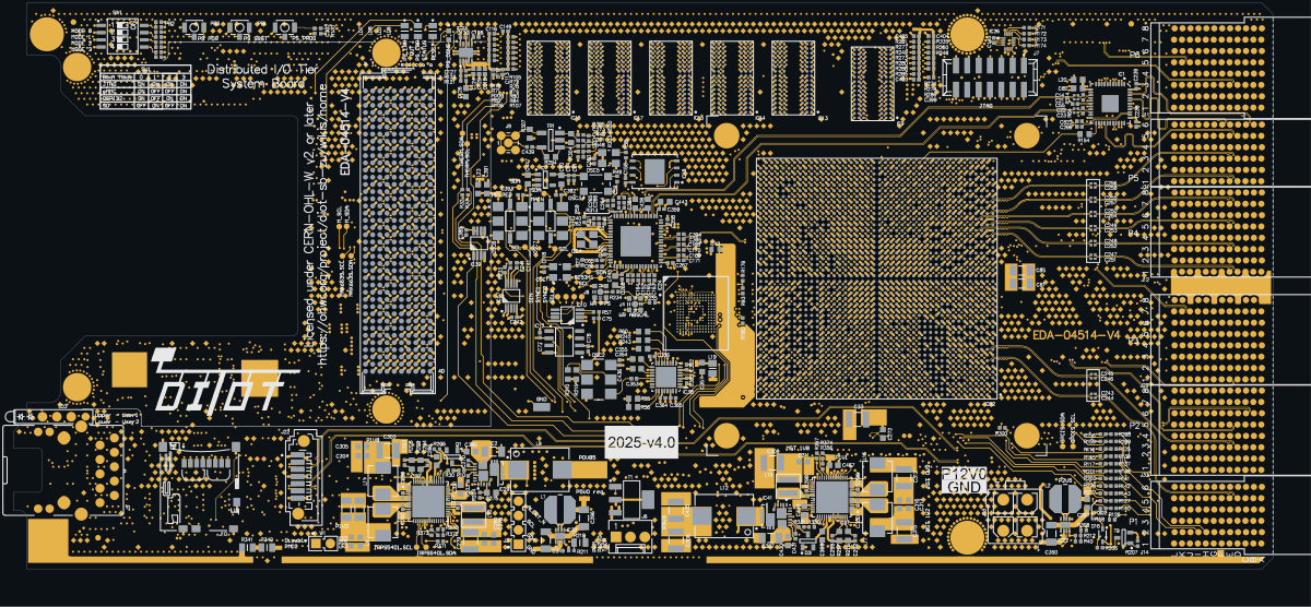
Design review
Probe recorded 46 findings: 5 blocker · 21 major · 20 minor (281 items) on this design. Each is shown here with its reasoning; the full review links every one to the pins, nets and datasheet pages it rests on.
USB-JTAG translator IC4 drives PS_SRST_B push-pull through R324, fighting the MAX16025's open-drain reset output
IC4 (SN74AVC2T245, USB-JTAG translator) drives PS_SRST_B push-pull through R324 (0R), fighting the open-drain OUT2 of the MAX16025 supervisor IC27. With a USB cable plugged in and no JTAG pod, the supervisor's power-on and brown-out reset of the MPSoC is defeated.
Where it is
IC4 carries the FT4232H "TRSTn" (ADBUS7) to the JTAG side. Its B-port outputs are push-pull. PS_SRST_B is otherwise a wired-OR built around the open-drain supervisor output.
Item Value Source IC4 A1 (pin 8) USB_TRSTn (FT4232H ADBUS7), R369 10k to P3V3_USB, so high unless the FTDI drives it low netlist IC4 B1 (pin 5) USB_JTAG.TRSTn netlist IC4 DIR1 (pin 10) / OE (pin 2) P3V3_USB (A to B) / EN_USB_JTAG_N netlist IC4 VCCA / VCCB P3V3_USB / P3V3 netlist R324 0R, fitted (no "No" marker on sheet 13), USB_JTAG.TRSTn to PS_SRST_B netlist; sheet 13 Other PS_SRST_B members IC27 pin 10 (MAX16025 OUT2), IC52.AB27, J7.14, R46 4k7 to P3V3, R45 0R to FMC_JTAG.TRST netlist EN_USB_JTAG_N R43 10k to P3V3_USB, pulled low by T18; T18 gate EN_USB_JTAG has R336 10k to P3V3 and only J7 pin 13 grounds it netlist SN74AVC2T245, OE low with DIR high drives the B port (push-pull CMOS) from A SN74AVC2T245 datasheet, p.12 MAX16025 outputs open-drain; absolute maximum +/-20 mA per pin MAX16025 datasheet, p.1 and p.2 ``
mermaid flowchart LR F["FT4232H ADBUS7<br/>USB_TRSTn, idles high"] --> I["IC4 A1 to B1<br/>push-pull"] I -- "R324 0R" --> N["PS_SRST_B"] S["IC27 MAX16025 OUT2<br/>open-drain"] --> N N --> Z["IC52.AB27"] N -- "R45" --> T["FMC TRST_L"]``When it happens
Whenever P3V3_USB is present (USB cable plugged in) and no JTAG pod grounds J7 pin 13, T18 holds OE low and IC4 is enabled. A1 idles high, so IC4 actively drives PS_SRST_B HIGH.
- during P3V3 power-up, when the supervisor is trying to hold OUT2 low for its programmed delay (CDLY2, noted on sheet 13);
- on any later supervisor-initiated reset.
Why it matters
- The push-pull high wins over the open-drain low: the supervisor's power-on and brown-out assertion of PS_SRST_B is defeated.
- OUT2 is stressed toward its 20 mA pin limit.
- PS_SRST_B also drives FMC TRST_L through R45, so the mezzanine TAP reset is affected too.
Suggested fix: make this path open-drain, for example by driving an open-drain buffer or FET from USB_TRSTn, or by using the A2/B2 channel to gate an N-FET, instead of connecting a push-pull translator output to the reset net.
PS UART level translator IC50 drives the Zynq's 3.3 V MIO bank 502 at 1.8 V (VCCB on P1V8), so UART0 RX never reaches VIH
IC50 (SN74AVC2T245) drives the PS console UART receive line UART_PS_RXD into PS_MIO66 of IC52 at 1.8 V (its VCCB is P1V8), but MIO66 sits in PS bank 502, which runs at 3.3 V; a 1.8 V high is below the 2.0 V LVCMOS33 VIH, so the PS UART console will not receive reliably, or at all.
The signal chain
Item Value Source IC50 VCCA (pin 7) P3V3_USB, FT4232H side netlist IC50 VCCB (pin 6) P1V8 netlist; schematic sheet 4 IC50 A2 (pin 9) to B2 (pin 4) FTDI_UART_PS_TXD to UART_PS_RXD netlist IC50 B1 (pin 5) UART_PS_TXD netlist UART_PS_RXD / UART_PS_TXD IC52 AD33 (PS_MIO66) / AE30 (PS_MIO67) netlist VCCO_PSIO2_502 (AC30, AG32) P3V3 netlist, bank map Designer's note on bank 502 "BANK 502 and PHY are powered from P3V3 to not overload the P1V8" schematic sheet 16 B-port output level follows VCCB, so at most 1.8 V here SN74AVC2T245 datasheet, p.3 pin table PS MIO LVCMOS33 VIH min 2.000 V (VIL max 0.800 V) DS925 Table 12, p.18 ``
mermaid flowchart LR F["FT4232H<br/>FTDI_UART_PS_TXD"] --> A["IC50 A2<br/>VCCA = P3V3_USB"] A --> B["IC50 B2<br/>VCCB = P1V8"] B -- "UART_PS_RXD, high at most 1.8 V" --> M["IC52 AD33 PS_MIO66<br/>bank 502 at 3.3 V, VIH 2.0 V"]``Why it matters
The FTDI-to-Zynq receive direction (A2 to B2 to MIO66) never presents a guaranteed logic high to the PS UART0 receiver. The bank voltage is fixed in copper (VCCO_PSIO2_502 on P3V3), so no constraint change can fix it.
The other direction is fine
The Zynq transmit direction (MIO67 at 3.3 V into IC50 B1) works. The SN74AVC2T245 recommended operating input voltage is 0 V to 3.6 V on the data inputs whatever the port supply (datasheet p.5), and at VCCB = 1.8 V the B-port VIH is 0.65 x VCCB, about 1.2 V (p.4), so a 3.3 V high is a valid, in-spec input. (The "4.6 V" figure on p.4 is the absolute-maximum rating, not an operating condition, so it is not the reason this direction is safe.)
IC51, the PL UART translator, is correct: its VCCB is P1V8 and it lands on HP bank 68, whose VCCO is P1V8. This suggests IC50's VCCB was not moved when bank 502 was changed to 3.3 V.
Fix: tie IC50 pin 6 (VCCB) to P3V3, matching bank 502.
DDR4 VPP (P2V5) is gated behind P3V3_PG while VDD (P1V2) has no interlock: as documented, VPP ramps after VDD; only IRPS5401 timing settings can reverse that (CERN #384)
DDR4 VPP (P2V5, from IC22) is enabled only by P3V3 power-good, and nothing holds DDR4 VDD (P1V2) back until VPP is up. With the sequence the designer documents (sheet 26), VPP ramps after VDD on all six devices (IC9, IC13-IC17), against the DRAM's VPP-first rule. Only IRPS5401 timing settings can reverse the order, and if P3V3 never reaches power-good the DRAMs sit with VDD and no VPP indefinitely.
The enable chain
The six DDR4 devices (IC9, IC13-IC17, MT40A1G16TB) take VDD/VDDQ from P1V2 and VPP (balls B1, R9) from P2V5.
Item Value Source P1V2 IC30 (IRPS5401) switcher C, FB_C (pin 15) netlist IC30 EN_A/B/C/D/L all on NetIC30_28, R309 10k to P5V_REG, so P1V2's start is set only by its TON_DELAY netlist IC31 EN_A/B/C/D/L (pins 42, 44, 51, 53, 28) P1V8AUX_PG, driven by IC30 PG_B (pin 30) netlist P3V3_PG IC31 PG_A (pin 26), R225 pull-up to P3V3_REG; IC23 EN also on it netlist P2V5 regulator IC22 TPS62125, a 300 mA part fed from P12V0, EN (pin 3) = P3V3_PG netlist Designer's sequencing note "P1V2, P1V8, then P3V3 then P2V5" schematic sheet 26 Micron rule "VPP must ramp at the same time or up to 10 minutes prior to VDD, and VPP must be equal to or higher than VDD at all times" Micron MT40A1G16 datasheet, p.37 ``
mermaid flowchart LR A["IC30 up<br/>P1V2 after its TON_DELAY"] --> B["P1V8_AUX good<br/>P1V8AUX_PG"] B --> C["IC31<br/>P3V3"] C --> D["P3V3_PG"] D --> E["IC22<br/>P2V5 = VPP"]``What CERN found
[diot-sb-zu #384](https://gitlab.com/ohwr/project/diot-sb-zu/-/issues/384) "DDR power sequence" (2026-04, closed) confirms the as-configured order 1V2 → 2V5/0V6 against the datasheet's 2V5 → 1V2 → 0V6. CERN then reached the recommended order "by reducing 3V3_PG threshold ... and increasing IC30 1V2 channel's TON_DELAY", for its V5 configuration. The IRPS5401 configuration this board carries is not on file.
Why it matters
- As documented, VPP follows VDD on every power-up.
- A configuration fix turns the order into a timing race between IC30's 1V2 delay and the P3V3 power-good chain.
- If IC31 or IC41 (P3V3) fails to reach power-good, the DRAMs sit with VDD applied and no VPP indefinitely.
Fix: bring P2V5 up first or together with P1V2 by construction, for example by enabling IC22 from P5V_REG or P12V0 rather than from P3V3_PG.
- PowerGroundShortblockerOpen
'GND' carries a power pin (IC30.22) and a ground pin (IC16.A2)
Net 'GND' connects a power pin (IC30.22) and a ground pin (IC16.A2).
At GND
- NetCopperSplitblockerOpen
CHASSIS's copper is in 2 pieces: B2.1, B3.1, M3.1 and R41.1 are not connected to the rest of the net
CHASSIS's copper is in 2 pieces: B2.1, B3.1, M3.1 and R41.1 are not connected to the rest of the net. Piece 1: B1.1, B4.1, C24.1, J2.6, J5.SHIELD, M4.1 and R341.2, on TOP_LAYER, L3, L5, L7, L8, L10, L12 and BOTTOM_LAYER, 5 drill(s), 195.84 mm2 of pour, over (89.21, 80) to (157.33, 113.57). Piece 2: B2.1, B3.1, M3.1 and R41.1, on TOP_LAYER, L3, L5, L7, L8, L10, L12 and BOTTOM_LAYER, 3 drill(s), over (91.9, 165.12) to (157.33, 176.4). The export files every one of these pins under the net, so every connectivity check passes; the copper the fab builds leaves them apart. Usually a pour island that touches only one via of its own net, or a track ending short of its copper: join the piece to the net and export again.
At split:CHASSIS
Board over-temperature shutdown cycles power instead of latching: the LM75 sensors that disable IC30 are powered from P3V3, a rail that shutdown removes
The board over-temperature shutdown cycles power instead of latching: the LM75A sensors IC36, IC39 and IC40 that disable IC30 are powered from P3V3, a rail that the shutdown itself removes. A board that stays hot power-cycles the FPGA, DDR4 and every other rail repeatedly.
Where it is
Item Value Source OVERTHERM_N open-drain O.S. outputs of IC36, IC39, IC40 (LM75A, pin 3) netlist OVERTHERM_N to IC30 enables R252 (0R) to NetIC30_28, the tied EN_A/B/C/D/L pins of IC30 netlist NetIC30_28 pull-up R309 10k to P5V_REG netlist LM75A +VS (pin 8) P3V3 netlist P3V3 source IC41 under IC31 switcher A netlist IC31 enable P1V8AUX_PG (IC30 PG_B) only netlist The loop
``
mermaid flowchart LR A["LM75A O.S. asserts<br/>T_OS passed"] --> B["IC30 shuts down"] B --> C["P1V8AUX_PG drops<br/>IC31 off"] C --> D["P3V3 collapses"] D --> E["LM75A loses supply<br/>O.S. releases"] E --> F["IC30 re-enables<br/>full sequence again"] F --> A``Why it matters
Per the TI datasheet (p.11), the LM75A "always powers up in a known state" (comparator mode, T_OS 80 C, T_HYST 75 C), and below about 1.7 V the registers are reset to those defaults.
- Any threshold, hysteresis or fault-queue setting that firmware wrote is lost at the first trip.
- A board that stays hot power-cycles the FPGA, DDR4 and every other rail repeatedly instead of staying off.
Whether the repeated restart harms anything depends on how hot the board gets and on the IRPS5401 MTP settings, which are not on file. The dependency loop itself is fixed by the wiring.
Suggested fix: powering the sensors from an always-on rail (P3V3_REG, which already powers the I2C mux and the IRPS5401 VDDIO) would make the trip hold until the board cools below T_HYST.
P0V85 power-stage 92 C over-temperature trip relies on the BSS138 gate threshold (0.85-1.5 V), so the real trip point ranges from 92 C up to the TDA21535's own 140 C
The designed 92 C over-temperature trip on the P0V85 power stage IC29 relies on the gate threshold of T10 (BSS138, 0.85-1.5 V). On a high-threshold T10 the trip moves to about 220 C, so only the TDA21535's own 140 C fault would shut the board down.
The signal chain
IC29 (TDA21535, the 30 A P0V85 power stage) reports temperature on TMON/FLT (OTP_MAIN). Sheet 25 divides it onto the gate of T10, whose drain pulls the IC30 enable net low.
``
mermaid flowchart LR A["IC29 TDA21535<br/>OTP_MAIN, pin 1"] --> B["R370 1k + R372 4k7<br/>R373 10k to GND"] B -- "gain 0.637" --> C["T10 BSS138 gate<br/>NetR372_1"] C --> D["R371 0R"] D --> E["NetIC30_28<br/>IC30 enables"]``The numbers
Quantity Value Source TMON/FLT slope 0.6 V + 8 mV/C TDA21535 datasheet, p.12 Divider gain 10 / 15.7 = 0.637 derived from R370 1k, R372 4k7, R373 10k (netlist) Designer's intent "@92 C Votp = 1.336V", "Vth= 0.85V" schematic sheet 25 note BSS138 V_GS(th) at I_D = 1 mA 0.85 V min to 1.5 V max onsemi BSS138LT1G datasheet, p.2 V_otp needed at V_GS(th) = 1.5 V 1.5 / 0.637 = 2.36 V derived Temperature at that V_otp (2.36 - 0.6) / 0.008 = 220 C derived TDA21535 own over-temperature flag rising 140 C, "TMON/FLT pulled up high" TDA21535 datasheet, p.9 So 0.85 V is the most favourable part, not a nominal. The real trip point ranges from 92 C up to the TDA21535's own 140 C.
Why it matters
- On a high-threshold T10 the designed 92 C shutdown never acts, and only the power stage's internal 140 C fault shuts the board down.
- Near threshold T10 conducts only partly against the 10k pull-up, which gives a soft, temperature-dependent EN level rather than a clean trip.
Suggested fix: a comparator or a supervisor with a defined threshold, or reading OTP_MAIN through IC30/IC28 telemetry, would give the intended 92 C.
Only P1V8_AUX and P3V3 power-good are checked: a failed P0V85, P1V2, P1V8 or MGT rail leaves the MPSoC partly powered with PS_POR_B released
Only the P1V8_AUX and P3V3 power-goods are used. The PG outputs for P0V85, P1V2, P1V8 and the MGT rails on IC30/IC31 are unconnected, so a single failed rail leaves the MPSoC partly powered, with IC27 releasing PS_POR_B 400 ms after P3V3 regardless.
The power-good chain as wired
- IC30 PG_B (P1V8_AUX, net P1V8AUX_PG) enables all of IC31.
- IC31 PG_A (P3V3, net P3V3_PG) enables IC22/IC23, and is what IC27 (MAX16025) watches before releasing PS_POR_B.
- IC27 IN1/IN2 (pins 2, 3, NetIC27_2) are both on the P3V3 divider R176 68k / R178 13k, with CDLY1 100 nF (400 ms per the sheet 13 note). OUT1 (pin 11) is PS_POR_B.
``
mermaid flowchart LR A["IC30 PG_B<br/>P1V8AUX_PG"] --> B["IC31 enables"] B --> C["IC31 PG_A<br/>P3V3_PG"] C --> D["IC22 / IC23"] P["P3V3 divider<br/>R176 / R178"] --> E["IC27 MAX16025"] E -- "400 ms" --> F["PS_POR_B released"]``Unconnected power-good outputs
Device Pin Rail Source IC30 PG_A (pin 26) P0V85 netlist: $NONE$ IC30 PG_C (pin 27) P1V2 netlist: $NONE$ IC30 PG_D (pin 16) P1V8 netlist: $NONE$ IC31 PG_B/C/D/L (pins 30, 27, 16, 25) MGT_1V8, MGT_0V9, MGT_1V2, P1V1 netlist: $NONE$ Why it matters
If P0V85 (VCCINT, VCC_PSINTLP/FP), P1V2 (VCCO_PSDDR and the DDR4 VDD), P1V8 or MGT_1V2 (which also feeds VCC_PSPLL through net tie NT7) fails or trips, nothing holds off the other rails. P3V3 VCCO, MGTAVTT and the rest stay up, and PS_POR_B is released 400 ms after P3V3 regardless.
- DS925 (p.35, Table 37 note 1) requires PS_POR_B to be held low "after all the PS supply voltages reach minimum levels".
- DS925 PL/GT sequencing (p.16) puts VCCINT first so that I/Os are 3-stated and MGTAVTT current stays within spec.
Whether IC30/IC31 shut all their loops together on a fault (global_fault_en) is an MTP setting that is not on file; it could mitigate part of this. As wired, a single-rail failure leaves the device partly powered and out of reset.
Fix: wiring the unused PG outputs (open-drain) into P1V8AUX_PG/P3V3_PG, or into the IC27 inputs, would close this.
IC31 MTP strap R217 (3.48k) selects MTP segment +5, but the schematic note says IC31 uses segment 6
The IC31 (IRPS5401) MTP strap R217 = 3k48 selects MTP segment +5, but the schematic note on sheet 26 says IC31 uses segment 6. If the configuration is written to segment 6 as the note says, IC31 loads segment 5 at power-up and comes up with the wrong or an empty configuration.
The numbers
The IRPS5401 reads its configuration from one of 15 MTP segments, picked by the resistor on the MTP pin.
Quantity Value Source MTP resistor table 2.87 kOhm = +4, 3.48 kOhm = +5, 4.12 kOhm = +6 IRPS5401 datasheet, Table 9, p.25 IC30 MTP (pin 54, NetC294_2) R209 = 2k87 to GND, so segment +4 netlist / BOM IC30 note "MTP segment selected: 4", which matches schematic IC31 MTP (pin 54, NetC295_2) R217 = 3k48 0.1% to GND, with C295 10 nF, so segment +5 netlist / BOM IC31 note "MTP segment selected: 6 / MTP resistor 3480 ohms" schematic sheet 26 IC31 ADDR_PROT R216, equal 3k48, offset +5, giving I2C address 0x15 in the same note schematic sheet 26 The equal 3k48 on ADDR_PROT shows that the resistor value is deliberate, so the segment number in the note is the error.
Why it matters
Both parts are marked "unprogrammed part and need prior configuration to work". IC31 makes MGT_0V9, MGT_1V2, MGT_1V8, P3V3 and P1V1. The configuration file is not on file, so which segment it targets cannot be checked here.
Fix: the note should say segment 5, or R217 should be 4.12k. Whichever is chosen must match the programming file.
IC3 (MIC5219-3.3, P3V3_USB) output has only ultra-low-ESR MLCCs; the datasheet asks for about 1 ohm ESR and warns ultra-low ESR can cause oscillation
IC3 (MIC5219-3.3YM5, making P3V3_USB) has only ultra-low-ESR ceramic output capacitors. The datasheet asks for an ESR of about 1 ohm or less and warns that ultra-low-ESR capacitors could cause oscillation.
Where it is
IC3 makes P3V3_USB for the FT4232H (IC46), its EEPROM and the USB-side level translators.
Quantity Value Source Bulk output capacitor C160, 22 uF 0603 6.3 V X5R netlist / BOM: CC0603_22UF_6.3V_20%_X5R Small output capacitors eleven 100 nF 0402 X7R: C53, C375, C449, C450, C458, C460-C462, C464, C465, C478 netlist / BOM Total on P3V3_USB about 23 uF, all ceramic, ESR in the milliohm range derived Tantalum or series-resistor element none netlist BYP (pin 4) unconnected, so the 1 uF minimum applies; it is met netlist What the datasheet says
Microchip MIC5219 datasheet, p.13, 4.3 Output Capacitor: "The output capacitor should have an ESR (equivalent series resistance) of about 1 ohm or less and a resonant frequency above 1 MHz. Ultra-low ESR capacitors could cause oscillation and/or under-damped transient response. Most tantalum or aluminum electrolytic capacitors are adequate". Its application circuits show tantalum output capacitors.
Why it matters
The ESR class the datasheet asks for is not met. Whether the fitted combination actually oscillates is not established here; the datasheet only says it could.
Suggested fix: a small series resistor (about 0.5-1 ohm) in series with C160, or a tantalum/polymer output capacitor, would put the loop in the range the datasheet characterises. Alternatively, confirm stability by measurement on the built board.
eMMC IC24 RST_n (1.8 V VCCQ domain) is tied to PS_POR_B, which is pulled up to 3.3 V
The eMMC IC24 RST_n ball (K5) is in the 1.8 V VCCQ domain but is wired to PS_POR_B, which R168 pulls up to 3.3 V. Every power-on reset release drives RST_n about 1.5 V above the eMMC's I/O supply.
Where it is
Item Value Source IC24 VCCQ (ball C6) P1V8 (bank 500, 1.8 V) netlist IC24 VCC (balls E6/F5) P3V3 netlist IC24 RST_n (ball K5) PS_POR_B netlist; sheet 11 PS_POR_B driver IC27 pin 11 (MAX16025 OUT1, open-drain) netlist; sheet 13 PS_POR_B pull-up R168 4k7 to P3V3 (no "No" marker on sheet 13) netlist; sheet 13 Other load IC52.W27 PS_POR_B, config bank 503 at 3.3 V netlist VCCQ options 1.8 V or 3.3 V; this design uses 1.8 V, so the I/O cells, RST_n included, are 1.8 V cells Kingston EMMC16G datasheet, p.2 ``
mermaid flowchart LR M["IC27 MAX16025<br/>OUT1 open-drain"] --> N["PS_POR_B"] R["R168 4k7<br/>to P3V3"] --> N N --> Z["IC52.W27<br/>bank 503, 3.3 V"] N -- "3.3 V" --> E["IC24.K5 RST_n<br/>VCCQ = 1.8 V"]``Why it matters
- RST_n is driven to 3.3 V every time the board comes out of power-on reset, and it also rises while VCCQ may still be ramping.
- The Kingston datasheet on file has no absolute-maximum or signal-level table, so nothing permits this.
- The eMMC standard places RST_n in the VCCQ domain (JESD84, not on file here), and the input's clamp to VCCQ will conduct through R168.
The datasheet notes (Table 7, p.9) that RST_n is disabled by default and may be left unconnected.
Suggested fix: leave RST_n open, drive it from a 1.8 V MIO/GPIO, or add a divider or level shifter from PS_POR_B. This is a reset line crossing voltage domains.
PS DDR4 ECC device IC17: unused-byte UDM_n/UDBI_n (E2) left floating; Micron requires a 10k pull-up to VDDQ
On the PS DDR4 ECC device IC17, ball E2 (UDM_n/UDBI_n) of the unused upper byte is left floating. Micron requires a 10k pull-up to VDDQ there.
Where it is
IC17 carries only the ECC byte of the PS DDR4 (lower byte: DQ64-71, DM8, DQS8). Its unused upper byte is terminated as follows:
Upper-byte pin As built Micron x16 rule (datasheet p.20) Source UDQS_t (B7) to GND through R157 200R one rail through about 200 ohm netlist; sheet 9 UDQS_c (A7) to P1V2 through R114 200R opposite rail through about 200 ohm netlist; sheet 9 E2 UDM_n/UDBI_n no-connect, floating ($NONE$) to VDDQ through a large (10k) pull-up netlist; sheet 9 no-connect cross DQ8-DQ15 unconnected may be pulled up or floated netlist The strobes are terminated as Micron specifies. Only DQ[15:8] are allowed to float.
Why it matters
A floating DM/DBI input sits at an undefined level, and it is subject to the ODT settings the controller programs for data mask, so it can draw crowbar current or toggle with noise. Functional impact is expected to be low, because the upper byte's strobes are static.
Suggested fix: add a 10k pull-up from IC17 E2 to P1V2.
eMMC CMD line has no pull-up (DAT0-7 have 10k to P1V8); CMD is open-drain during eMMC initialization
The eMMC IC24 CMD line (EMMC_CMD / PS_EMMC.CMD) has no pull-up, while all eight DAT lines have 10k to P1V8. CMD is open-drain during eMMC initialization, so enumeration relies entirely on the Zynq MIO21 internal pull-up.
Where it is
Item Value Source EMMC_CMD IC24.M5 (CMD) and R189.2 only netlist PS_EMMC.CMD IC52.AF35 (MIO21) and R189.1 only netlist Series resistor R189 = 30R netlist Pull-up on either side of R189 none netlist; sheet 11 EMMC_D0-D7 pull-ups 10k to P1V8 each (R20-R22, R93, R98, R99, R179, R180) netlist; sheet 11 pull-up bank Vendor board rule "A 10 kΩ pull-up resistor is recommended on CMD" (JEDEC JESD84-B451 requires pull-ups on DAT0-7) AMD UG583 v1.29, p.206 CMD drive mode open-drain for initialization, push-pull for fast command transfer Kingston EMMC16G datasheet, p.9 Why it matters
During initialization (device identification, CMD1/CMD2/CMD3) the device can only pull CMD low. The high level, and the ability of several responders to share the line, depend on a pull-up; AMD's own PCB guideline recommends a 10 kΩ pull-up on CMD (UG583 p.206).
Without a board resistor, enumeration relies on the Zynq MIO21 internal pull-up being enabled by boot ROM/FSBL configuration. That was not verified here, and it is weak compared with a board resistor.
Severity: major
IC24 is a selectable boot device (mode 0110). If CMD does not reach a valid high during the open-drain identification phase, eMMC boot fails. The board omits a resistor the FPGA vendor recommends. The MIO21 internal pull-up may mask it, but that is not a designed margin and was not verified, so it does not lower the severity.
Suggested fix: add a 10k (4.7k-50k) pull-up from EMMC_CMD to P1V8, matching the DAT lines.
BAT54C went end-of-life (Obsolete)
Vendor (DigiKey) lifecycle for BAT54C (onsemi's listing) changed from "Active" to "Obsolete" since this board was reviewed. Placed as D9. A sourcing/longevity risk; consider a replacement before production.
BZX84C3V3 went end-of-life (Obsolete)
Vendor (DigiKey) lifecycle for BZX84C3V3 (onsemi's listing) changed from "Active" to "Obsolete" since this board was reviewed. Placed as D1, D3. A sourcing/longevity risk; consider a replacement before production.
- concernCON-001majorOpen
[eol:BAT54C:Obsolete] BAT54C lifecycle changed from "Active" to "Obsolete" since this board was reviewed: OHWR0083 R4 DIOT SB ZU. A sourcing and longevity risk. Should this be replaced before the next build?
- concernCON-002majorOpen
[eol:BZX84C3V3:Obsolete] BZX84C3V3 lifecycle changed from "Active" to "Obsolete" since this board was reviewed: OHWR0083 R4 DIOT SB ZU. A sourcing and longevity risk. Should this be replaced before the next build?
- DuplicatePassivemajorOpen
'DCXO_OE' is pulled to 'GND' by 2 fitted resistors (R246 (10k), R247 (10k))
'DCXO_OE' is pulled to 'GND' by 2 fitted resistors: R246 (10k), R247 (10k) — 5k effective. A pull-up's value is specified, and two of them in parallel is not the value that was specified — presence checks are satisfied by either one and cannot see the pair. Which one is intended? Removing the duplicate, or recording that the parallel value is deliberate, both settle it; leaving two identical resistors on one node does not.
At DCXO_OE
- DiffPairMismatchmajorOpen
'RTN_P' / 'RTN_N' (pair inferred from names) is pin-count asymmetric (3 vs 2)
Differential pair 'RTN_P' / 'RTN_N', INFERRED FROM THE NET NAMES (nothing in the design declares it a pair), is pin-count asymmetric (3 vs 2) - one side reaches a pin the other does not, so the two halves cannot be routed as a matched pair. NOTE: this check does not verify WHICH contact either net reaches; a correctly-symmetric pair can still be swapped at a connector.
At RTN_P
- DecapOrdermajorOpen
DecapOrder: 8 components×8
Checked by the review, stands · Claude walker D2 (cern-01 session) — Checked on R4 (IC9, IC13-IC17 DDR4, IC24 eMMC, IC2 Si5341): the distances are read from placement and are correct as stated. This is a layout-practice heuristic (Probe's starting thresholds), not a datasheet requirement: Micron's DDR4 and Xilinx UG583 decoupling guidance on file does not fix the order of 68-470 nF vs 1-4.7 uF parts at the 1-5 mm scale, where via and plane-spreading inductance usually dominate. Not refutable with a citation; left open for the owner.
At IC13, IC14, IC15, IC16, IC17, IC2, IC24, IC9
Each finding, with its own headline
IC13IC13 supply pins A9, B9, D9, J1, L1 on 'P1V2': the smallest capacitor C205 sits 4.5 mm away, behind C197 at 2.4 mm
IC13 supply pins A9, B9, D9, J1, L1 on 'P1V2': the smallest capacitor C205 sits 4.5 mm away, behind C197 at 2.4 mm. IC13.A9: the smallest value, C205 (68 nF), is 4.5 mm from the pin and C197 (4.7 uF) 2.4 mm: the high-frequency part sits behind more inductance than the bulk part, which needs it least. IC13.B9: the smallest value, C205 (68 nF), is 4.8 mm from the pin and C197 (4.7 uF) 1.8 mm: the high-frequency part sits behind more inductance than the bulk part, which needs it least. IC13.D9: the smallest value, C217 (68 nF), is 3.8 mm from the pin and C197 (4.7 uF) 1.3 mm: the high-frequency part sits behind more inductance than the bulk part, which needs it least. IC13.J1: the smallest value, C215 (470 nF), is 2.7 mm from the pin and C214 (4.7 uF) 1.3 mm: the high-frequency part sits behind more inductance than the bulk part, which needs it least. IC13.L1: the smallest value, C211 (470 nF), is 3.8 mm from the pin and C214 (4.7 uF) 2.3 mm: the high-frequency part sits behind more inductance than the bulk part, which needs it least. Swap them, or bring the smallest value to the pin: it serves the fastest current and is the one the loop inductance defeats. Distances are pad centre to pin centre in the board plane. The 5 mm radius, the 10x value step and the 1 mm / 1.5x tie tolerance are Probe's starting values.
IC14IC14 supply pins D9, F2, G1, J1, J2 on 'P1V2': the smallest capacitor C222 sits 3.8 mm away, behind C195 at 1.3 mm
IC14 supply pins D9, F2, G1, J1, J2 on 'P1V2': the smallest capacitor C222 sits 3.8 mm away, behind C195 at 1.3 mm. IC14.D9: the smallest value, C222 (68 nF), is 3.8 mm from the pin and C195 (4.7 uF) 1.3 mm: the high-frequency part sits behind more inductance than the bulk part, which needs it least. IC14.F2: the smallest value, C217 (68 nF), is 4.5 mm from the pin and C219 (4.7 uF) 2.9 mm: the high-frequency part sits behind more inductance than the bulk part, which needs it least. IC14.G1: the smallest value, C217 (68 nF), is 3.4 mm from the pin and C219 (4.7 uF) 1.8 mm: the high-frequency part sits behind more inductance than the bulk part, which needs it least. IC14.J1: the smallest value, C217 (68 nF), is 3.2 mm from the pin and C219 (4.7 uF) 1.3 mm: the high-frequency part sits behind more inductance than the bulk part, which needs it least. IC14.J2: the smallest value, C217 (68 nF), is 4.0 mm from the pin and C219 (4.7 uF) 2.0 mm: the high-frequency part sits behind more inductance than the bulk part, which needs it least. Swap them, or bring the smallest value to the pin: it serves the fastest current and is the one the loop inductance defeats. Distances are pad centre to pin centre in the board plane. The 5 mm radius, the 10x value step and the 1 mm / 1.5x tie tolerance are Probe's starting values.
IC15IC15 supply pins D9, F2, G1, J1, J2 on 'P1V2': the smallest capacitor C188 sits 2.9 mm away, behind C176 at 1.3 mm
IC15 supply pins D9, F2, G1, J1, J2 on 'P1V2': the smallest capacitor C188 sits 2.9 mm away, behind C176 at 1.3 mm. IC15.D9: the smallest value, C188 (68 nF), is 2.9 mm from the pin and C176 (4.7 uF) 1.3 mm: the high-frequency part sits behind more inductance than the bulk part, which needs it least. IC15.F2: the smallest value, C222 (68 nF), is 4.5 mm from the pin and C196 (4.7 uF) 2.8 mm: the high-frequency part sits behind more inductance than the bulk part, which needs it least. IC15.G1: the smallest value, C222 (68 nF), is 3.4 mm from the pin and C196 (4.7 uF) 1.7 mm: the high-frequency part sits behind more inductance than the bulk part, which needs it least. IC15.J1: the smallest value, C222 (68 nF), is 3.2 mm from the pin and C196 (4.7 uF) 1.2 mm: the high-frequency part sits behind more inductance than the bulk part, which needs it least. IC15.J2: the smallest value, C222 (68 nF), is 4.0 mm from the pin and C196 (4.7 uF) 2.0 mm: the high-frequency part sits behind more inductance than the bulk part, which needs it least. Swap them, or bring the smallest value to the pin: it serves the fastest current and is the one the loop inductance defeats. Distances are pad centre to pin centre in the board plane. The 5 mm radius, the 10x value step and the 1 mm / 1.5x tie tolerance are Probe's starting values.
IC16IC16 supply pins D9, F8, G7 on 'P1V2': the smallest capacitor C192 sits 2.4 mm away, behind C174 at 1.3 mm
IC16 supply pins D9, F8, G7 on 'P1V2': the smallest capacitor C192 sits 2.4 mm away, behind C174 at 1.3 mm. IC16.D9: the smallest value, C192 (68 nF), is 2.4 mm from the pin and C174 (4.7 uF) 1.3 mm: the high-frequency part sits behind more inductance than the bulk part, which needs it least. IC16.F8: the smallest value, C192 (68 nF), is 2.0 mm from the pin and C177 (4.7 uF) 0.5 mm: the high-frequency part sits behind more inductance than the bulk part, which needs it least. IC16.G7: the smallest value, C192 (68 nF), is 2.8 mm from the pin and C177 (4.7 uF) 1.6 mm: the high-frequency part sits behind more inductance than the bulk part, which needs it least. Swap them, or bring the smallest value to the pin: it serves the fastest current and is the one the loop inductance defeats. Distances are pad centre to pin centre in the board plane. The 5 mm radius, the 10x value step and the 1 mm / 1.5x tie tolerance are Probe's starting values.
IC17IC17 supply pins D9, F2, G1, J1, J2 on 'P1V2': the smallest capacitor C184 sits 2.9 mm away, behind C175 at 1.3 mm
IC17 supply pins D9, F2, G1, J1, J2 on 'P1V2': the smallest capacitor C184 sits 2.9 mm away, behind C175 at 1.3 mm. IC17.D9: the smallest value, C184 (68 nF), is 2.9 mm from the pin and C175 (4.7 uF) 1.3 mm: the high-frequency part sits behind more inductance than the bulk part, which needs it least. IC17.F2: the smallest value, C208 (68 nF), is 4.5 mm from the pin and C194 (4.7 uF) 2.8 mm: the high-frequency part sits behind more inductance than the bulk part, which needs it least. IC17.G1: the smallest value, C208 (68 nF), is 3.5 mm from the pin and C194 (4.7 uF) 1.7 mm: the high-frequency part sits behind more inductance than the bulk part, which needs it least. IC17.J1: the smallest value, C208 (68 nF), is 3.2 mm from the pin and C194 (4.7 uF) 1.1 mm: the high-frequency part sits behind more inductance than the bulk part, which needs it least. IC17.J2: the smallest value, C208 (68 nF), is 4.0 mm from the pin and C194 (4.7 uF) 1.9 mm: the high-frequency part sits behind more inductance than the bulk part, which needs it least. Swap them, or bring the smallest value to the pin: it serves the fastest current and is the one the loop inductance defeats. Distances are pad centre to pin centre in the board plane. The 5 mm radius, the 10x value step and the 1 mm / 1.5x tie tolerance are Probe's starting values.
IC2IC2 supply pins 22, 26, 29, 36, 40, 57 on 'P1V8_CLK': the smallest capacitor C268 sits 1.8 mm away, behind C444 at 0.8 mm
IC2 supply pins 22, 26, 29, 36, 40, 57 on 'P1V8_CLK': the smallest capacitor C268 sits 1.8 mm away, behind C444 at 0.8 mm. IC2.22: the smallest value, C268 (100 nF), is 1.8 mm from the pin and C444 (1 uF) 0.8 mm: the high-frequency part sits behind more inductance than the bulk part, which needs it least. IC2.26: the smallest value, C268 (100 nF), is 3.4 mm from the pin and C444 (1 uF) 1.2 mm: the high-frequency part sits behind more inductance than the bulk part, which needs it least. IC2.29: the smallest value, C129 (100 nF), is 2.8 mm from the pin and C136 (1 uF) 0.2 mm: the high-frequency part sits behind more inductance than the bulk part, which needs it least. IC2.36: the smallest value, C267 (100 nF), is 2.0 mm from the pin and C263 (1 uF) 0.9 mm: the high-frequency part sits behind more inductance than the bulk part, which needs it least. IC2.40: the smallest value, C69 (100 nF), is 1.6 mm from the pin and C422 (1 uF) 0.4 mm: the high-frequency part sits behind more inductance than the bulk part, which needs it least. IC2.57: the smallest value, C359 (100 nF), is 4.5 mm from the pin and C123 (1 uF) 0.9 mm: the high-frequency part sits behind more inductance than the bulk part, which needs it least. Swap them, or bring the smallest value to the pin: it serves the fastest current and is the one the loop inductance defeats. Distances are pad centre to pin centre in the board plane. The 5 mm radius, the 10x value step and the 1 mm / 1.5x tie tolerance are Probe's starting values.
IC24IC24 supply pins P3, P5 on 'P1V8': the smallest capacitor C56 sits 1.6 mm away, behind C288 at 0.4 mm
IC24 supply pins P3, P5 on 'P1V8': the smallest capacitor C56 sits 1.6 mm away, behind C288 at 0.4 mm. IC24.P3: the smallest value, C56 (100 nF), is 1.6 mm from the pin and C288 (2.2 uF) 0.4 mm: the high-frequency part sits behind more inductance than the bulk part, which needs it least. IC24.P5: the smallest value, C56 (100 nF), is 2.1 mm from the pin and C288 (2.2 uF) 1.0 mm: the high-frequency part sits behind more inductance than the bulk part, which needs it least. Swap them, or bring the smallest value to the pin: it serves the fastest current and is the one the loop inductance defeats. Distances are pad centre to pin centre in the board plane. The 5 mm radius, the 10x value step and the 1 mm / 1.5x tie tolerance are Probe's starting values.
IC9IC9 supply pins B9, D9, R1 on 'P1V2': the smallest capacitor C418 sits 1.6 mm away, behind C423 at 0.4 mm
IC9 supply pins B9, D9, R1 on 'P1V2': the smallest capacitor C418 sits 1.6 mm away, behind C423 at 0.4 mm. IC9.B9: the smallest value, C418 (470 nF), is 1.6 mm from the pin and C423 (4.7 uF) 0.4 mm: the high-frequency part sits behind more inductance than the bulk part, which needs it least. IC9.D9: the smallest value, C414 (220 nF), is 3.8 mm from the pin and C413 (4.7 uF) 1.4 mm: the high-frequency part sits behind more inductance than the bulk part, which needs it least. IC9.R1: the smallest value, C416 (68 nF), is 2.7 mm from the pin and C412 (4.7 uF) 0.4 mm: the high-frequency part sits behind more inductance than the bulk part, which needs it least. Swap them, or bring the smallest value to the pin: it serves the fastest current and is the one the loop inductance defeats. Distances are pad centre to pin centre in the board plane. The 5 mm radius, the 10x value step and the 1 mm / 1.5x tie tolerance are Probe's starting values.
- EsdProtectorPlacementmajorOpen
EsdProtectorPlacement: 39 components×39
Checked by the review, stands · Claude walker D2 (cern-01 session) — Checked on R4 against the routed copper (protection cards of run 601's predecessor 418). They stand as measured. Backplane arrays D2, D5-D8 sit 12-35 mm from the J14/J33 contacts behind a via, against the PESD3V3L5UY data sheet p10 guidance: raised as OBS-622 (minor). JTAG arrays D13/D14 on spurs off J7: OBS-42. microSD arrays D11/D12: flow-through, 2.5-6.2 mm from J10, the one via being the top-to-bottom change to reach a clamp placed under the slot; D12.6 (card detect) reached on a 25 mm branch. Left open for the owner.
At D11, D12, D13, D14, D2, D5 and 3 more
Each finding, with its own headline
D11D11.1 on 'SDIO_CLK': 1 via(s) between J10.5 and D11.1
D11 (D3V3F4U6S) protects 'SDIO_CLK' at J10.5. Along the copper: 3.39 mm of track from the contact, 1 via(s) before it, the line runs through its pad (flow-through); the line runs 113.58 mm on to R490.2; D11 sits at J10, within 0 mm of the nearest place outside it to the contact: the track to it is mostly the escape out of J10's own pins, which no placement shortens.
1 via(s) between J10.5 and D11.1: the strike reaches an inner layer before it is clamped.
Measured on the copper the ODB states: tracks, the pads they land on, and the netlist's vias. Not a straight line between centroids.
D11D11.3 on 'SDIO_CMD': 1 via(s) between J10.3 and D11.3
D11 (D3V3F4U6S) protects 'SDIO_CMD' at J10.3. Along the copper: 2.55 mm of track from the contact, 1 via(s) before it, the line runs through its pad (flow-through); the line runs 115.93 mm on to R489.2; D11 sits at J10, within 0 mm of the nearest place outside it to the contact: the track to it is mostly the escape out of J10's own pins, which no placement shortens.
1 via(s) between J10.3 and D11.3: the strike reaches an inner layer before it is clamped.
Measured on the copper the ODB states: tracks, the pads they land on, and the netlist's vias. Not a straight line between centroids.
D11D11.4 on 'SDIO_DAT2': 1 via(s) between J10.1 and D11.4
D11 (D3V3F4U6S) protects 'SDIO_DAT2' at J10.1. Along the copper: 5.8 mm of track from the contact, 1 via(s) before it, the line runs through its pad (flow-through); the line runs 112.64 mm on to R487.2; D11 sits at J10, within 0 mm of the nearest place outside it to the contact: the track to it is mostly the escape out of J10's own pins, which no placement shortens.
1 via(s) between J10.1 and D11.4: the strike reaches an inner layer before it is clamped.
Measured on the copper the ODB states: tracks, the pads they land on, and the netlist's vias. Not a straight line between centroids.
D11D11.6 on 'SDIO_DAT3': 1 via(s) between J10.2 and D11.6
D11 (D3V3F4U6S) protects 'SDIO_DAT3' at J10.2. Along the copper: 6.24 mm of track from the contact, 1 via(s) before it, the line runs through its pad (flow-through); the line runs 113.5 mm on to R488.2; D11 sits at J10, within 0 mm of the nearest place outside it to the contact: the track to it is mostly the escape out of J10's own pins, which no placement shortens.
1 via(s) between J10.2 and D11.6: the strike reaches an inner layer before it is clamped.
Measured on the copper the ODB states: tracks, the pads they land on, and the netlist's vias. Not a straight line between centroids.
D12D12.1 on 'SDIO_DAT1': 1 via(s) between J10.8 and D12.1
D12 (D3V3F4U6S) protects 'SDIO_DAT1' at J10.8. Along the copper: 2.57 mm of track from the contact, 1 via(s) before it, the line runs through its pad (flow-through); the line runs 110.76 mm on to R486.2; D12 sits at J10, within 0 mm of the nearest place outside it to the contact: the track to it is mostly the escape out of J10's own pins, which no placement shortens.
1 via(s) between J10.8 and D12.1: the strike reaches an inner layer before it is clamped.
Measured on the copper the ODB states: tracks, the pads they land on, and the netlist's vias. Not a straight line between centroids.
D12D12.3 on 'SDIO_DAT0': 1 via(s) between J10.7 and D12.3
D12 (D3V3F4U6S) protects 'SDIO_DAT0' at J10.7. Along the copper: 2.8 mm of track from the contact, 1 via(s) before it, the line runs through its pad (flow-through); the line runs 111.72 mm on to R485.2; D12 sits at J10, within 0 mm of the nearest place outside it to the contact: the track to it is mostly the escape out of J10's own pins, which no placement shortens.
1 via(s) between J10.7 and D12.3: the strike reaches an inner layer before it is clamped.
Measured on the copper the ODB states: tracks, the pads they land on, and the netlist's vias. Not a straight line between centroids.
D12D12.6 on 'SDIO_DETECT': 2 via(s) between J10.12 and D12.6
D12 (D3V3F4U6S) protects 'SDIO_DETECT' at J10.12. Along the copper: 26.65 mm of track from the contact, 2 via(s) before it, on a 25.05 mm branch off the line; the line runs 2.25 mm on to R149.1; D12 sits 13.28 mm farther from the contact than the nearest place outside J10.
2 via(s) between J10.12 and D12.6: the strike reaches an inner layer before it is clamped. D12.6 hangs 25.05 mm off the line (limit 1 mm, default: no datasheet figure on file): the line carries the strike past it while the clamp is reached through the branch.
Measured on the copper the ODB states: tracks, the pads they land on, and the netlist's vias. Not a straight line between centroids.
D13D13.1 on 'PS_SRST_B': D13.1 hangs 5.23 mm off the line (limit 1 mm, default
D13 (PESD3V3L5UY) protects 'PS_SRST_B' at J7.14. Along the copper: 5.23 mm of track from the contact, 0 via(s) before it, on a 5.23 mm branch off the line; the line runs 0 mm on to R46.1; D13 sits 3.17 mm farther from the contact than the nearest place outside J7.
D13.1 hangs 5.23 mm off the line (limit 1 mm, default: no datasheet figure on file): the line carries the strike past it while the clamp is reached through the branch.
Measured on the copper the ODB states: tracks, the pads they land on, and the netlist's vias. Not a straight line between centroids.
D13D13.1 on 'PS_SRST_B': D13.1 hangs 5.23 mm off the line (limit 1 mm, default
D13 (PESD3V3L5UY) protects 'PS_SRST_B' at R45.2, where a strike from J1.d34 through R45 enters the net. Along the copper: 5.23 mm of track from the contact, 0 via(s) before it, on a 5.23 mm branch off the line; the line runs 0 mm on to R46.1; D13 sits 3.9 mm farther from the contact than the nearest place outside R45.
No protection network is recognised at the entry: R45 (0) is in series at the entry, but 0 ohm is below the 100 ohm that limits a strike, so it is not counted as a protection network.
D13.1 hangs 5.23 mm off the line (limit 1 mm, default: no datasheet figure on file): the line carries the strike past it while the clamp is reached through the branch.
Measured on the copper the ODB states: tracks, the pads they land on, and the netlist's vias. Not a straight line between centroids.
D13D13.3 on 'JTAG_TDI': D13.3 hangs 5.45 mm off the line (limit 1 mm, default
D13 (PESD3V3L5UY) protects 'JTAG_TDI' at J7.10. Along the copper: 5.45 mm of track from the contact, 0 via(s) before it, on a 5.45 mm branch off the line; the line runs 0 mm on to R54.1; D13 sits at J7, within 0 mm of the nearest place outside it to the contact: the track to it is mostly the escape out of J7's own pins, which no placement shortens.
D13.3 hangs 5.45 mm off the line (limit 1 mm, default: no datasheet figure on file): the line carries the strike past it while the clamp is reached through the branch.
Measured on the copper the ODB states: tracks, the pads they land on, and the netlist's vias. Not a straight line between centroids.
D13D13.4 on 'JTAG_TMS': D13.4 hangs 5.74 mm off the line (limit 1 mm, default
D13 (PESD3V3L5UY) protects 'JTAG_TMS' at J7.4. Along the copper: 5.74 mm of track from the contact, 0 via(s) before it, on a 5.74 mm branch off the line; the line runs 0 mm on to R51.1; D13 sits at J7, within 1.32 mm of the nearest place outside it to the contact: the track to it is mostly the escape out of J7's own pins, which no placement shortens.
D13.4 hangs 5.74 mm off the line (limit 1 mm, default: no datasheet figure on file): the line carries the strike past it while the clamp is reached through the branch.
Measured on the copper the ODB states: tracks, the pads they land on, and the netlist's vias. Not a straight line between centroids.
D13D13.5 on 'JTAG_TCK': D13.5 hangs 4.01 mm off the line (limit 1 mm, default
D13 (PESD3V3L5UY) protects 'JTAG_TCK' at J7.6. Along the copper: 4.01 mm of track from the contact, 0 via(s) before it, on a 4.01 mm branch off the line; the line runs 0 mm on to R52.1; D13 sits at J7, within 0 mm of the nearest place outside it to the contact: the track to it is mostly the escape out of J7's own pins, which no placement shortens.
D13.5 hangs 4.01 mm off the line (limit 1 mm, default: no datasheet figure on file): the line carries the strike past it while the clamp is reached through the branch.
Measured on the copper the ODB states: tracks, the pads they land on, and the netlist's vias. Not a straight line between centroids.
D13D13.6 on 'FMC_JTAG.TDO': 3 via(s) between J1.d31 and D13.6
D13 (PESD3V3L5UY) protects 'FMC_JTAG.TDO' at J1.d31. Along the copper: 186.41 mm of track from the contact, 3 via(s) before it, on a 174.1 mm branch off the line; the line runs 13.57 mm on to IC5.2; D13 sits 103.75 mm farther from the contact than the nearest place outside J1.
3 via(s) between J1.d31 and D13.6: the strike reaches an inner layer before it is clamped. D13.6 hangs 174.1 mm off the line (limit 1 mm, default: no datasheet figure on file): the line carries the strike past it while the clamp is reached through the branch. D13 joins the line 12.31 mm from J1.d31 on a 13.57 mm run to IC5.2: nearer the far end than the contact, so the surge travels most of the line before it is clamped.
Measured on the copper the ODB states: tracks, the pads they land on, and the netlist's vias. Not a straight line between centroids.
D13D13.6 on 'FMC_JTAG.TDO': D13.6 hangs 2.88 mm off the line (limit 1 mm, default
D13 (PESD3V3L5UY) protects 'FMC_JTAG.TDO' at J7.8. Along the copper: 2.88 mm of track from the contact, 0 via(s) before it, on a 2.88 mm branch off the line; the line runs 0 mm on to R53.1; D13 sits at J7, within 0 mm of the nearest place outside it to the contact: the track to it is mostly the escape out of J7's own pins, which no placement shortens.
D13.6 hangs 2.88 mm off the line (limit 1 mm, default: no datasheet figure on file): the line carries the strike past it while the clamp is reached through the branch.
Measured on the copper the ODB states: tracks, the pads they land on, and the netlist's vias. Not a straight line between centroids.
D14D14.3 on 'EN_USB_JTAG': 1 via(s) between J7.13 and D14.3
D14 (PESD3V3L5UY) protects 'EN_USB_JTAG' at J7.13. Along the copper: 3.03 mm of track from the contact, 1 via(s) before it, on a 1.33 mm branch off the line; the line runs 204.21 mm on to C172.2; D14 sits at J7, within 0 mm of the nearest place outside it to the contact: the track to it is mostly the escape out of J7's own pins, which no placement shortens.
1 via(s) between J7.13 and D14.3: the strike reaches an inner layer before it is clamped. D14.3 hangs 1.33 mm off the line (limit 1 mm, default: no datasheet figure on file): the line carries the strike past it while the clamp is reached through the branch.
Measured on the copper the ODB states: tracks, the pads they land on, and the netlist's vias. Not a straight line between centroids.
D2D2.1 on 'NetD2_1': 1 via(s) between J14.F2 and D2.1
D2 (PESD3V3L5UY) protects 'NetD2_1' at J14.F2. Along the copper: 15.61 mm of track from the contact, 1 via(s) before it, the line runs through its pad (flow-through); the line runs 20.99 mm on to R127.2; D2 sits 9.63 mm farther from the contact than the nearest place outside J14.
1 via(s) between J14.F2 and D2.1: the strike reaches an inner layer before it is clamped. D2 joins the line 15.61 mm from J14.F2 on a 20.99 mm run to R127.2: nearer the far end than the contact, so the surge travels most of the line before it is clamped.
Measured on the copper the ODB states: tracks, the pads they land on, and the netlist's vias. Not a straight line between centroids.
D2D2.3 on 'NetD2_3': 1 via(s) between J14.H3 and D2.3
D2 (PESD3V3L5UY) protects 'NetD2_3' at J14.H3. Along the copper: 11.98 mm of track from the contact, 1 via(s) before it, on a 1.02 mm branch off the line; the line runs 17.77 mm on to R140.2; D2 sits 4.5 mm farther from the contact than the nearest place outside J14.
1 via(s) between J14.H3 and D2.3: the strike reaches an inner layer before it is clamped. D2.3 hangs 1.02 mm off the line (limit 1 mm, default: no datasheet figure on file): the line carries the strike past it while the clamp is reached through the branch. D2 joins the line 10.96 mm from J14.H3 on a 17.77 mm run to R140.2: nearer the far end than the contact, so the surge travels most of the line before it is clamped.
Measured on the copper the ODB states: tracks, the pads they land on, and the netlist's vias. Not a straight line between centroids.
D2D2.4 on 'NetD2_4': 1 via(s) between J14.E2 and D2.4
D2 (PESD3V3L5UY) protects 'NetD2_4' at J14.E2. Along the copper: 21.6 mm of track from the contact, 1 via(s) before it, on a 1.02 mm branch off the line; the line runs 22.9 mm on to R126.2; D2 sits 11.01 mm farther from the contact than the nearest place outside J14.
1 via(s) between J14.E2 and D2.4: the strike reaches an inner layer before it is clamped. D2.4 hangs 1.02 mm off the line (limit 1 mm, default: no datasheet figure on file): the line carries the strike past it while the clamp is reached through the branch. D2 joins the line 20.58 mm from J14.E2 on a 22.9 mm run to R126.2: nearer the far end than the contact, so the surge travels most of the line before it is clamped.
Measured on the copper the ODB states: tracks, the pads they land on, and the netlist's vias. Not a straight line between centroids.
D2D2.5 on 'CPCIS_I2C.SDA': D2 joins the line 21.74 mm from J14.C2 on a 23.74 mm run to R221.1
D2 (PESD3V3L5UY) protects 'CPCIS_I2C.SDA' at J14.C2. Along the copper: 21.74 mm of track from the contact, 0 via(s) before it, the line runs through its pad (flow-through); the line runs 23.74 mm on to R221.1; D2 sits 13.77 mm farther from the contact than the nearest place outside J14.
D2 joins the line 21.74 mm from J14.C2 on a 23.74 mm run to R221.1: nearer the far end than the contact, so the surge travels most of the line before it is clamped.
Measured on the copper the ODB states: tracks, the pads they land on, and the netlist's vias. Not a straight line between centroids.
D2D2.6 on 'NetD2_6': 1 via(s) between J14.L2 and D2.6
D2 (PESD3V3L5UY) protects 'NetD2_6' at J14.L2. Along the copper: 11.45 mm of track from the contact, 1 via(s) before it, the line runs through its pad (flow-through); the line runs 14.16 mm on to R220.2; D2 sits 1.63 mm farther from the contact than the nearest place outside J14.
1 via(s) between J14.L2 and D2.6: the strike reaches an inner layer before it is clamped. D2 joins the line 11.45 mm from J14.L2 on a 14.16 mm run to R220.2: nearer the far end than the contact, so the surge travels most of the line before it is clamped.
Measured on the copper the ODB states: tracks, the pads they land on, and the netlist's vias. Not a straight line between centroids.
D5D5.1 on 'NetD5_1': 1 via(s) between J14.H2 and D5.1
D5 (PESD3V3L5UY) protects 'NetD5_1' at J14.H2. Along the copper: 15.93 mm of track from the contact, 1 via(s) before it, the line runs through its pad (flow-through); the line runs 23.88 mm on to R139.2; D5 sits 8.05 mm farther from the contact than the nearest place outside J14.
1 via(s) between J14.H2 and D5.1: the strike reaches an inner layer before it is clamped. D5 joins the line 15.93 mm from J14.H2 on a 23.88 mm run to R139.2: nearer the far end than the contact, so the surge travels most of the line before it is clamped.
Measured on the copper the ODB states: tracks, the pads they land on, and the netlist's vias. Not a straight line between centroids.
D5D5.3 on 'NetD5_3': 1 via(s) between J14.I2 and D5.3
D5 (PESD3V3L5UY) protects 'NetD5_3' at J14.I2. Along the copper: 13.67 mm of track from the contact, 1 via(s) before it, the line runs through its pad (flow-through); the line runs 19.92 mm on to R141.2; D5 sits 6.84 mm farther from the contact than the nearest place outside J14.
1 via(s) between J14.I2 and D5.3: the strike reaches an inner layer before it is clamped. D5 joins the line 13.67 mm from J14.I2 on a 19.92 mm run to R141.2: nearer the far end than the contact, so the surge travels most of the line before it is clamped.
Measured on the copper the ODB states: tracks, the pads they land on, and the netlist's vias. Not a straight line between centroids.
D5D5.4 on 'NetD5_4': D5 joins the line 11.63 mm from J14.K3 on a 14.59 mm run to R143.2
D5 (PESD3V3L5UY) protects 'NetD5_4' at J14.K3. Along the copper: 11.63 mm of track from the contact, 0 via(s) before it, the line runs through its pad (flow-through); the line runs 14.59 mm on to R143.2; D5 sits 1.77 mm farther from the contact than the nearest place outside J14.
D5 joins the line 11.63 mm from J14.K3 on a 14.59 mm run to R143.2: nearer the far end than the contact, so the surge travels most of the line before it is clamped.
Measured on the copper the ODB states: tracks, the pads they land on, and the netlist's vias. Not a straight line between centroids.
D5D5.5 on 'CPCIS_I2C.SCL': 1 via(s) between J14.B2 and D5.5
D5 (PESD3V3L5UY) protects 'CPCIS_I2C.SCL' at J14.B2. Along the copper: 27.61 mm of track from the contact, 1 via(s) before it, on a 1.02 mm branch off the line; the line runs 27.52 mm on to R301.1; D5 sits 15.83 mm farther from the contact than the nearest place outside J14.
1 via(s) between J14.B2 and D5.5: the strike reaches an inner layer before it is clamped. D5.5 hangs 1.02 mm off the line (limit 1 mm, default: no datasheet figure on file): the line carries the strike past it while the clamp is reached through the branch. D5 joins the line 26.59 mm from J14.B2 on a 27.52 mm run to R301.1: nearer the far end than the contact, so the surge travels most of the line before it is clamped.
Measured on the copper the ODB states: tracks, the pads they land on, and the netlist's vias. Not a straight line between centroids.
D5D5.6 on 'NetD5_6': D5 joins the line 13.3 mm from J14.J3 on a 16.26 mm run to R142.2
D5 (PESD3V3L5UY) protects 'NetD5_6' at J14.J3. Along the copper: 13.3 mm of track from the contact, 0 via(s) before it, the line runs through its pad (flow-through); the line runs 16.26 mm on to R142.2; D5 sits 2.55 mm farther from the contact than the nearest place outside J14.
D5 joins the line 13.3 mm from J14.J3 on a 16.26 mm run to R142.2: nearer the far end than the contact, so the surge travels most of the line before it is clamped.
Measured on the copper the ODB states: tracks, the pads they land on, and the netlist's vias. Not a straight line between centroids.
D6D6.1 on 'NetD6_1': 1 via(s) between J33.C8 and D6.1
D6 (PESD3V3L5UY) protects 'NetD6_1' at J33.C8. Along the copper: 26.81 mm of track from the contact, 1 via(s) before it, on a 1.02 mm branch off the line; the line runs 33.72 mm on to R265.2; D6 sits 18.18 mm farther from the contact than the nearest place outside J33.
1 via(s) between J33.C8 and D6.1: the strike reaches an inner layer before it is clamped. D6.1 hangs 1.02 mm off the line (limit 1 mm, default: no datasheet figure on file): the line carries the strike past it while the clamp is reached through the branch. D6 joins the line 25.79 mm from J33.C8 on a 33.72 mm run to R265.2: nearer the far end than the contact, so the surge travels most of the line before it is clamped.
Measured on the copper the ODB states: tracks, the pads they land on, and the netlist's vias. Not a straight line between centroids.
D6D6.3 on 'NetD6_3': 1 via(s) between J33.J7 and D6.3
D6 (PESD3V3L5UY) protects 'NetD6_3' at J33.J7. Along the copper: 12.81 mm of track from the contact, 1 via(s) before it, the line runs through its pad (flow-through); the line runs 20.93 mm on to R270.2; D6 sits 6.55 mm farther from the contact than the nearest place outside J33.
1 via(s) between J33.J7 and D6.3: the strike reaches an inner layer before it is clamped. D6 joins the line 12.81 mm from J33.J7 on a 20.93 mm run to R270.2: nearer the far end than the contact, so the surge travels most of the line before it is clamped.
Measured on the copper the ODB states: tracks, the pads they land on, and the netlist's vias. Not a straight line between centroids.
D6D6.4 on 'NetD6_4': 1 via(s) between J33.B8 and D6.4
D6 (PESD3V3L5UY) protects 'NetD6_4' at J33.B8. Along the copper: 31.71 mm of track from the contact, 1 via(s) before it, on a 1.02 mm branch off the line; the line runs 34.43 mm on to R264.2; D6 sits 19.47 mm farther from the contact than the nearest place outside J33.
1 via(s) between J33.B8 and D6.4: the strike reaches an inner layer before it is clamped. D6.4 hangs 1.02 mm off the line (limit 1 mm, default: no datasheet figure on file): the line carries the strike past it while the clamp is reached through the branch. D6 joins the line 30.69 mm from J33.B8 on a 34.43 mm run to R264.2: nearer the far end than the contact, so the surge travels most of the line before it is clamped.
Measured on the copper the ODB states: tracks, the pads they land on, and the netlist's vias. Not a straight line between centroids.
D6D6.6 on 'NetD6_6': 1 via(s) between J33.E7 and D6.6
D6 (PESD3V3L5UY) protects 'NetD6_6' at J33.E7. Along the copper: 19.84 mm of track from the contact, 1 via(s) before it, the line runs through its pad (flow-through); the line runs 24.61 mm on to R267.2; D6 sits 12.74 mm farther from the contact than the nearest place outside J33.
1 via(s) between J33.E7 and D6.6: the strike reaches an inner layer before it is clamped. D6 joins the line 19.84 mm from J33.E7 on a 24.61 mm run to R267.2: nearer the far end than the contact, so the surge travels most of the line before it is clamped.
Measured on the copper the ODB states: tracks, the pads they land on, and the netlist's vias. Not a straight line between centroids.
D7D7.1 on 'NetD7_1': 1 via(s) between J14.C3 and D7.1
D7 (PESD3V3L5UY) protects 'NetD7_1' at J14.C3. Along the copper: 23.94 mm of track from the contact, 1 via(s) before it, on a 1.02 mm branch off the line; the line runs 31.8 mm on to R125.2; D7 sits 12.79 mm farther from the contact than the nearest place outside J14.
1 via(s) between J14.C3 and D7.1: the strike reaches an inner layer before it is clamped. D7.1 hangs 1.02 mm off the line (limit 1 mm, default: no datasheet figure on file): the line carries the strike past it while the clamp is reached through the branch. D7 joins the line 22.92 mm from J14.C3 on a 31.8 mm run to R125.2: nearer the far end than the contact, so the surge travels most of the line before it is clamped.
Measured on the copper the ODB states: tracks, the pads they land on, and the netlist's vias. Not a straight line between centroids.
D7D7.3 on 'NetD7_3': 1 via(s) between J33.K7 and D7.3
D7 (PESD3V3L5UY) protects 'NetD7_3' at J33.K7. Along the copper: 20.35 mm of track from the contact, 1 via(s) before it, the line runs through its pad (flow-through); the line runs 29.46 mm on to R272.2; D7 sits 10.5 mm farther from the contact than the nearest place outside J33.
1 via(s) between J33.K7 and D7.3: the strike reaches an inner layer before it is clamped. D7 joins the line 20.35 mm from J33.K7 on a 29.46 mm run to R272.2: nearer the far end than the contact, so the surge travels most of the line before it is clamped.
Measured on the copper the ODB states: tracks, the pads they land on, and the netlist's vias. Not a straight line between centroids.
D7D7.4 on 'NetD7_4': 1 via(s) between J14.G3 and D7.4
D7 (PESD3V3L5UY) protects 'NetD7_4' at J14.G3. Along the copper: 21.33 mm of track from the contact, 1 via(s) before it, on a 1.02 mm branch off the line; the line runs 22.74 mm on to R138.2; D7 sits 7.73 mm farther from the contact than the nearest place outside J14.
1 via(s) between J14.G3 and D7.4: the strike reaches an inner layer before it is clamped. D7.4 hangs 1.02 mm off the line (limit 1 mm, default: no datasheet figure on file): the line carries the strike past it while the clamp is reached through the branch. D7 joins the line 20.31 mm from J14.G3 on a 22.74 mm run to R138.2: nearer the far end than the contact, so the surge travels most of the line before it is clamped.
Measured on the copper the ODB states: tracks, the pads they land on, and the netlist's vias. Not a straight line between centroids.
D7D7.5 on 'NetD7_5': 1 via(s) between J33.A7 and D7.5
D7 (PESD3V3L5UY) protects 'NetD7_5' at J33.A7. Along the copper: 35.12 mm of track from the contact, 1 via(s) before it, on a 1.02 mm branch off the line; the line runs 39.11 mm on to R262.2; D7 sits 20.53 mm farther from the contact than the nearest place outside J33.
1 via(s) between J33.A7 and D7.5: the strike reaches an inner layer before it is clamped. D7.5 hangs 1.02 mm off the line (limit 1 mm, default: no datasheet figure on file): the line carries the strike past it while the clamp is reached through the branch. D7 joins the line 34.1 mm from J33.A7 on a 39.11 mm run to R262.2: nearer the far end than the contact, so the surge travels most of the line before it is clamped.
Measured on the copper the ODB states: tracks, the pads they land on, and the netlist's vias. Not a straight line between centroids.
D7D7.6 on 'NetD7_6': 1 via(s) between J14.F3 and D7.6
D7 (PESD3V3L5UY) protects 'NetD7_6' at J14.F3. Along the copper: 23.47 mm of track from the contact, 1 via(s) before it, the line runs through its pad (flow-through); the line runs 24.84 mm on to R137.2; D7 sits 8.96 mm farther from the contact than the nearest place outside J14.
1 via(s) between J14.F3 and D7.6: the strike reaches an inner layer before it is clamped. D7 joins the line 23.47 mm from J14.F3 on a 24.84 mm run to R137.2: nearer the far end than the contact, so the surge travels most of the line before it is clamped.
Measured on the copper the ODB states: tracks, the pads they land on, and the netlist's vias. Not a straight line between centroids.
D8D8.1 on 'NetD8_1': 1 via(s) between J33.D7 and D8.1
D8 (PESD3V3L5UY) protects 'NetD8_1' at J33.D7. Along the copper: 27.33 mm of track from the contact, 1 via(s) before it, the line runs through its pad (flow-through); the line runs 36.27 mm on to R266.2; D8 sits 15.33 mm farther from the contact than the nearest place outside J33.
1 via(s) between J33.D7 and D8.1: the strike reaches an inner layer before it is clamped. D8 joins the line 27.33 mm from J33.D7 on a 36.27 mm run to R266.2: nearer the far end than the contact, so the surge travels most of the line before it is clamped.
Measured on the copper the ODB states: tracks, the pads they land on, and the netlist's vias. Not a straight line between centroids.
D8D8.3 on 'NetD8_3': 1 via(s) between J33.B7 and D8.3
D8 (PESD3V3L5UY) protects 'NetD8_3' at J33.B7. Along the copper: 28.18 mm of track from the contact, 1 via(s) before it, the line runs through its pad (flow-through); the line runs 36.92 mm on to R263.2; D8 sits 17.83 mm farther from the contact than the nearest place outside J33.
1 via(s) between J33.B7 and D8.3: the strike reaches an inner layer before it is clamped. D8 joins the line 28.18 mm from J33.B7 on a 36.92 mm run to R263.2: nearer the far end than the contact, so the surge travels most of the line before it is clamped.
Measured on the copper the ODB states: tracks, the pads they land on, and the netlist's vias. Not a straight line between centroids.
D8D8.4 on 'NetD8_4': 1 via(s) between J33.H7 and D8.4
D8 (PESD3V3L5UY) protects 'NetD8_4' at J33.H7. Along the copper: 24.41 mm of track from the contact, 1 via(s) before it, on a 1.02 mm branch off the line; the line runs 28 mm on to R269.2; D8 sits 10.69 mm farther from the contact than the nearest place outside J33.
1 via(s) between J33.H7 and D8.4: the strike reaches an inner layer before it is clamped. D8.4 hangs 1.02 mm off the line (limit 1 mm, default: no datasheet figure on file): the line carries the strike past it while the clamp is reached through the branch. D8 joins the line 23.39 mm from J33.H7 on a 28 mm run to R269.2: nearer the far end than the contact, so the surge travels most of the line before it is clamped.
Measured on the copper the ODB states: tracks, the pads they land on, and the netlist's vias. Not a straight line between centroids.
D8D8.5 on 'NetD8_5': 1 via(s) between J33.G7 and D8.5
D8 (PESD3V3L5UY) protects 'NetD8_5' at J33.G7. Along the copper: 25.68 mm of track from the contact, 1 via(s) before it, on a 0.74 mm branch off the line; the line runs 30.58 mm on to R268.2; D8 sits 11.79 mm farther from the contact than the nearest place outside J33.
1 via(s) between J33.G7 and D8.5: the strike reaches an inner layer before it is clamped. D8 joins the line 24.94 mm from J33.G7 on a 30.58 mm run to R268.2: nearer the far end than the contact, so the surge travels most of the line before it is clamped.
Measured on the copper the ODB states: tracks, the pads they land on, and the netlist's vias. Not a straight line between centroids.
D8D8.6 on 'NetD8_6': 1 via(s) between J33.J8 and D8.6
D8 (PESD3V3L5UY) protects 'NetD8_6' at J33.J8. Along the copper: 21.23 mm of track from the contact, 1 via(s) before it, the line runs through its pad (flow-through); the line runs 27.06 mm on to R271.2; D8 sits 12.32 mm farther from the contact than the nearest place outside J33.
1 via(s) between J33.J8 and D8.6: the strike reaches an inner layer before it is clamped. D8 joins the line 21.23 mm from J33.J8 on a 27.06 mm run to R271.2: nearer the far end than the contact, so the surge travels most of the line before it is clamped.
Measured on the copper the ODB states: tracks, the pads they land on, and the netlist's vias. Not a straight line between centroids.
- PartLifecyclemajorOpen
PartLifecycle: 2 part numbers×2
2 Obsolete · on 3 placements
At D1, D9
Each finding, with its own headline
D1BZX84C3V3 on 2 placements (D1, D3): the distributor catalogue reports "Obsolete" for onsemi's BZX84C3V3
BZX84C3V3 on 2 placements (D1, D3): the distributor catalogue reports "Obsolete" for onsemi's BZX84C3V3 — a sourcing/longevity risk to confirm against the MANUFACTURER before acting. This board's BOM names FAIRCHILD SEMICONDUCTOR, and that is one line with onsemi: ON Semiconductor completed its acquisition of Fairchild Semiconductor on 2016-09-19 and renamed itself onsemi on 2021-08-05. A distributor delisting is not the same claim as the part being unavailable; check the vendor's own lifecycle/product-change notice for the status and any named successor. Re-read the source: GET /api/odb/parts/BZX84C3V3/providers (which provider said it, the maker and part number it matched, its own words, and when we asked). THE LAST BUY DATE HAS PASSED (2017-11-19, 3,283 day(s) ago), so this is a substitution rather than a buy. The distributor reports NONE left. No approved alternate is recorded for this position.
D9BAT54C on D9: the distributor catalogue reports "Obsolete" for onsemi's BAT54C
BAT54C on D9: the distributor catalogue reports "Obsolete" for onsemi's BAT54C — a sourcing/longevity risk to confirm against the MANUFACTURER before acting. This board's BOM names FAIRCHILD SEMICONDUCTOR, and that is one line with onsemi: ON Semiconductor completed its acquisition of Fairchild Semiconductor on 2016-09-19 and renamed itself onsemi on 2021-08-05. A distributor delisting is not the same claim as the part being unavailable; check the vendor's own lifecycle/product-change notice for the status and any named successor. Re-read the source: GET /api/odb/parts/BAT54C/providers (which provider said it, the maker and part number it matched, its own words, and when we asked). THE LAST BUY DATE HAS PASSED (2018-09-30, 2,968 day(s) ago), so this is a substitution rather than a buy. The distributor reports 54,983 left. No approved alternate is recorded for this position.
- PartLifecyclemajorOpen
PartLifecycle: 3 part numbers×3
3 Obsolete · on 22 placements
At IC13, IC24, T10
Each finding, with its own headline
IC13MT40A1G16TB-062E:F on 6 placements (IC13, IC14, IC15, IC16, IC17, IC9): the distributor catalogue reports "Obsolete" for Micron Technology Inc.'s MT40A1G16TB-062E:F
MT40A1G16TB-062E:F on 6 placements (IC13, IC14, IC15, IC16, IC17, IC9): the distributor catalogue reports "Obsolete" for Micron Technology Inc.'s MT40A1G16TB-062E:F — a sourcing/longevity risk to confirm against the MANUFACTURER before acting. That is the maker this board's BOM names (MICRON TECHNOLOGY). A distributor delisting is not the same claim as the part being unavailable; check the vendor's own lifecycle/product-change notice for the status and any named successor. Re-read the source: GET /api/odb/parts/MT40A1G16TB-062E:F/providers (which provider said it, the maker and part number it matched, its own words, and when we asked). No approved alternate is recorded for this position.
IC24EMMC16G-TB29-70H01 on IC24: the distributor catalogue reports "Obsolete" for Kingston Technology's EMMC16G-TB29-70H01
EMMC16G-TB29-70H01 on IC24: the distributor catalogue reports "Obsolete" for Kingston Technology's EMMC16G-TB29-70H01 — a sourcing/longevity risk to confirm against the MANUFACTURER before acting. That is the maker this board's BOM names (KINGSTON TECHNOLOGY). A distributor delisting is not the same claim as the part being unavailable; check the vendor's own lifecycle/product-change notice for the status and any named successor. Re-read the source: GET /api/odb/parts/EMMC16G-TB29-70H01/providers (which provider said it, the maker and part number it matched, its own words, and when we asked). THE LAST BUY DATE HAS PASSED (2024-03-31, 959 day(s) ago), so this is a substitution rather than a buy. The distributor reports NONE left. No approved alternate is recorded for this position.
T10BSS138L on 15 placements (T10, T11, T12, T13, T14, T15, T18, T2, …): the distributor catalogue reports "Obsolete" for onsemi's BSS138L
BSS138L on 15 placements (T10, T11, T12, T13, T14, T15, T18, T2, …): the distributor catalogue reports "Obsolete" for onsemi's BSS138L — a sourcing/longevity risk to confirm against the MANUFACTURER before acting. This board's BOM names ON SEMICONDUCTOR, and that is one line with onsemi: ON Semiconductor completed its acquisition of Fairchild Semiconductor on 2016-09-19 and renamed itself onsemi on 2021-08-05. A distributor delisting is not the same claim as the part being unavailable; check the vendor's own lifecycle/product-change notice for the status and any named successor. Re-read the source: GET /api/odb/parts/BSS138L/providers (which provider said it, the maker and part number it matched, its own words, and when we asked). THE LAST BUY DATE HAS PASSED (2026-01-01, 318 day(s) ago), so this is a substitution rather than a buy. The distributor reports NONE left. No approved alternate is recorded for this position.
- PartLifecyclemajorOpen
PartLifecycle: 4 part numbers×4
3 Obsolete, 1 Not For New Designs · on 5 placements
At IC18, IC6, IC7, OSC7
Each finding, with its own headline
IC18MT25QU01GBBB1EW9-0SIT on IC18: the distributor catalogue reports "Obsolete" for Micron Technology Inc.'s MT25QU01GBBB1EW9-0SIT
MT25QU01GBBB1EW9-0SIT on IC18: the distributor catalogue reports "Obsolete" for Micron Technology Inc.'s MT25QU01GBBB1EW9-0SIT — a sourcing/longevity risk to confirm against the MANUFACTURER before acting. That is the maker this board's BOM names (MICRON TECHNOLOGY). A distributor delisting is not the same claim as the part being unavailable; check the vendor's own lifecycle/product-change notice for the status and any named successor. Re-read the source: GET /api/odb/parts/MT25QU01GBBB1EW9-0SIT/providers (which provider said it, the maker and part number it matched, its own words, and when we asked). THE LAST BUY DATE HAS PASSED (2026-08-31, 76 day(s) ago), so this is a substitution rather than a buy. The distributor reports NONE left. No approved alternate is recorded for this position.
IC6PCA9548APW on IC6: the distributor catalogue reports "Obsolete" for NXP USA Inc.'s PCA9548APW,112
PCA9548APW on IC6: the distributor catalogue reports "Obsolete" for NXP USA Inc.'s PCA9548APW,112 — a sourcing/longevity risk to confirm against the MANUFACTURER before acting. That is the maker this board's BOM names (NXP SEMICONDUCTORS). A distributor delisting is not the same claim as the part being unavailable; check the vendor's own lifecycle/product-change notice for the status and any named successor. Re-read the source: GET /api/odb/parts/PCA9548APW/providers (which provider said it, the maker and part number it matched, its own words, and when we asked). THE LAST BUY DATE HAS PASSED (2018-01-24, 3,217 day(s) ago), so this is a substitution rather than a buy. The distributor reports NONE left. No approved alternate is recorded for this position.
IC7LP5951MF-3.0 on IC7: the distributor catalogue reports "Obsolete" for Texas Instruments's LP5951MF-3.0
LP5951MF-3.0 on IC7: the distributor catalogue reports "Obsolete" for Texas Instruments's LP5951MF-3.0 — a sourcing/longevity risk to confirm against the MANUFACTURER before acting. That is the maker this board's BOM names (TEXAS INSTRUMENTS). A distributor delisting is not the same claim as the part being unavailable; check the vendor's own lifecycle/product-change notice for the status and any named successor. Re-read the source: GET /api/odb/parts/LP5951MF-3.0/providers (which provider said it, the maker and part number it matched, its own words, and when we asked). No approved alternate is recorded for this position.
OSC7549BACB001937ABG on 2 placements (OSC7, OSC8): the distributor catalogue reports "Not For New Designs" for Skyworks Solutions Inc.'s 549BACB001937ABG
549BACB001937ABG on 2 placements (OSC7, OSC8): the distributor catalogue reports "Not For New Designs" for Skyworks Solutions Inc.'s 549BACB001937ABG — a sourcing/longevity risk to confirm against the MANUFACTURER before acting. This board's BOM names SILICON LABS, and that is one line with Skyworks Solutions Inc.: Skyworks completed its acquisition of Silicon Labs' Infrastructure & Automotive business (timing, isolation) on 2021-07-26; Silicon Labs still sells its other lines under its own name. A distributor delisting is not the same claim as the part being unavailable; check the vendor's own lifecycle/product-change notice for the status and any named successor. Re-read the source: GET /api/odb/parts/549BACB001937ABG/providers (which provider said it, the maker and part number it matched, its own words, and when we asked). No approved alternate is recorded for this position.
- ReferencePlaneDiscontinuitymajorOpen
ReferencePlaneDiscontinuity: 17 boards×17
Checked by the review, stands · Claude walker D2 (cern-01 session) — Checked on R4: the plane gaps, voids and via reference changes are read from the ODB++ copper and are as stated; whether each crossing matters depends on the signal's edge rate and return path, which is layout practice with no datasheet requirement on file to settle it (UG583 gives routing guidance, not a pass/fail per crossing). CERN's own V4 issues #376 and #389 record that some of this board's pairs change reference without stitching vias. Not refutable with a citation; left open for the owner.
At gap:L11PWR:hole 177.6,166.96|178.1,167.46, gap:L11PWR:hole 204.58,121.88|205.08,122.38, gap:L11PWR:hole 204.8,124.13|205.3,124.63, gap:L11PWR:hole 248.13,112.99|248.63,113.49, gap:L11PWR:hole 263.2,124.93|263.7,125.43, gap:L13GND:hole 100.6,158|139.23,160 and 11 more
Each finding, with its own headline
gap:L11PWR:hole 177.6,166.96|178.1,167.46'DDR4_PS.ODT' crosses one gap in L11PWR's negative-plane field at 1 place, the longest 0.45 mm (fastest: DDR4_PS.ODT at 100 ps 10-90 %, ASSUMED)
Along 'DDR4_PS.ODT' on L12, L11PWR is a negative layer (copper everywhere inside the profile), and its field is cleared for 0.45 mm under the track at (177.98, 167.21). The layer does not state the nets either side, so whether this is a split between two planes or a void in one is not said; either way the return current has to go round it. What cleared it: the hole at x 177.6..178.1, y 166.96..167.46. One decision covers the void: whether these tracks may cross it, or the plane should be filled under them. No crossing has a plane on the track's other side, so the whole return meets the break.
- 'DDR4_PS.ODT' on L12 at (177.98, 167.21), 0.45 mm; other side: no plane on L13GND
Every site is a row of this finding's evidence, keyed by net, layers and position. GET /api/odb/boards/84/reference-planes?group=gap%3AL11PWR%3Ahole%20177.6%2C166.96%7C178.1%2C167.46 serves each with its own layer_image region; all of them lie in x 176.85..179.3, y 166.21..168.21 mm (board frame, Y up).
Read from the copper as drawn on the reference layer, along each track's centreline at exact breakpoints. The reference is the copper beside the track, never the layer's type or name. Whether it matters depends on each signal's edge rate, which nothing on file states for these nets: a slow static line crosses a split harmlessly, a fast edge does not.
gap:L11PWR:hole 204.58,121.88|205.08,122.38'WR_DAC.DIN' crosses one gap in L11PWR's negative-plane field at 1 place, the longest 0.39 mm (fastest: WR_DAC.DIN at 100 ps 10-90 %, ASSUMED)
Along 'WR_DAC.DIN' on L12, L11PWR is a negative layer (copper everywhere inside the profile), and its field is cleared for 0.39 mm under the track at (204.91, 122.04). The layer does not state the nets either side, so whether this is a split between two planes or a void in one is not said; either way the return current has to go round it. What cleared it: the hole at x 204.58..205.08, y 121.88..122.38. One decision covers the void: whether these tracks may cross it, or the plane should be filled under them. No crossing has a plane on the track's other side, so the whole return meets the break.
- 'WR_DAC.DIN' on L12 at (204.91, 122.04), 0.39 mm; other side: no plane on L13GND
Every site is a row of this finding's evidence, keyed by net, layers and position. GET /api/odb/boards/84/reference-planes?group=gap%3AL11PWR%3Ahole%20204.58%2C121.88%7C205.08%2C122.38 serves each with its own layer_image region; all of them lie in x 203.83..206.1, y 120.85..123.13 mm (board frame, Y up).
Read from the copper as drawn on the reference layer, along each track's centreline at exact breakpoints. The reference is the copper beside the track, never the layer's type or name. Whether it matters depends on each signal's edge rate, which nothing on file states for these nets: a slow static line crosses a split harmlessly, a fast edge does not.
gap:L11PWR:hole 204.8,124.13|205.3,124.63'WR_DAC.SYNC1' crosses one gap in L11PWR's negative-plane field at 1 place, the longest 0.41 mm (fastest: WR_DAC.SYNC1 at 100 ps 10-90 %, ASSUMED)
Along 'WR_DAC.SYNC1' on L12, L11PWR is a negative layer (copper everywhere inside the profile), and its field is cleared for 0.41 mm under the track at (205.05, 124.5). The layer does not state the nets either side, so whether this is a split between two planes or a void in one is not said; either way the return current has to go round it. What cleared it: the hole at x 204.8..205.3, y 124.13..124.63. One decision covers the void: whether these tracks may cross it, or the plane should be filled under them. No crossing has a plane on the track's other side, so the whole return meets the break.
- 'WR_DAC.SYNC1' on L12 at (205.05, 124.5), 0.41 mm; other side: no plane on L13GND
Every site is a row of this finding's evidence, keyed by net, layers and position. GET /api/odb/boards/84/reference-planes?group=gap%3AL11PWR%3Ahole%20204.8%2C124.13%7C205.3%2C124.63 serves each with its own layer_image region; all of them lie in x 204.05..206.09, y 123.38..125.77 mm (board frame, Y up).
Read from the copper as drawn on the reference layer, along each track's centreline at exact breakpoints. The reference is the copper beside the track, never the layer's type or name. Whether it matters depends on each signal's edge rate, which nothing on file states for these nets: a slow static line crosses a split harmlessly, a fast edge does not.
gap:L11PWR:hole 248.13,112.99|248.63,113.49'SLOT4.LVDS_0_P' crosses one gap in L11PWR's negative-plane field at 1 place, the longest 0.56 mm (fastest: SLOT4.LVDS_0_P at 100 ps 10-90 %, ASSUMED)
Along 'SLOT4.LVDS_0_P' on L12, L11PWR is a negative layer (copper everywhere inside the profile), and its field is cleared for 0.56 mm under the track at (248.47, 113.15). The layer does not state the nets either side, so whether this is a split between two planes or a void in one is not said; either way the return current has to go round it. What cleared it: the hole at x 248.13..248.63, y 112.99..113.49. One decision covers the void: whether these tracks may cross it, or the plane should be filled under them. No crossing has a plane on the track's other side, so the whole return meets the break.
- 'SLOT4.LVDS_0_P' on L12 at (248.47, 113.15), 0.56 mm; other side: no plane on L13GND
Every site is a row of this finding's evidence, keyed by net, layers and position. GET /api/odb/boards/84/reference-planes?group=gap%3AL11PWR%3Ahole%20248.13%2C112.99%7C248.63%2C113.49 serves each with its own layer_image region; all of them lie in x 247.38..249.81, y 111.9..114.24 mm (board frame, Y up).
Read from the copper as drawn on the reference layer, along each track's centreline at exact breakpoints. The reference is the copper beside the track, never the layer's type or name. Whether it matters depends on each signal's edge rate, which nothing on file states for these nets: a slow static line crosses a split harmlessly, a fast edge does not.
gap:L11PWR:hole 263.2,124.93|263.7,125.43'NetC143_2' crosses one gap in L11PWR's negative-plane field at 1 place, the longest 0.46 mm (fastest: NetC143_2 at 100 ps 10-90 %, ASSUMED)
Along 'NetC143_2' on L12, L11PWR is a negative layer (copper everywhere inside the profile), and its field is cleared for 0.46 mm under the track at (263.45, 125.3). The layer does not state the nets either side, so whether this is a split between two planes or a void in one is not said; either way the return current has to go round it. 1 of them run ALONG the bare copper, parallel to its edges, rather than across it (the longest 0.33 mm). What cleared it: the hole at x 263.2..263.7, y 124.93..125.43. One decision covers the void: whether these tracks may cross it, or the plane should be filled under them. No crossing has a plane on the track's other side, so the whole return meets the break.
- 'NetC143_2' on L12 at (263.45, 125.3), 0.46 mm, running ALONG the bare copper for 0.33 mm, not across it; other side: no plane on L13GND
Every site is a row of this finding's evidence, keyed by net, layers and position. GET /api/odb/boards/84/reference-planes?group=gap%3AL11PWR%3Ahole%20263.2%2C124.93%7C263.7%2C125.43 serves each with its own layer_image region; all of them lie in x 262.42..264.45, y 124.18..126.63 mm (board frame, Y up).
Read from the copper as drawn on the reference layer, along each track's centreline at exact breakpoints. The reference is the copper beside the track, never the layer's type or name. Whether it matters depends on each signal's edge rate, which nothing on file states for these nets: a slow static line crosses a split harmlessly, a fast edge does not.
gap:L13GND:hole 100.6,158|139.23,160'NetIC27_6' crosses one gap in L13GND's negative-plane field at 1 place, the longest 12.97 mm (fastest: NetIC27_6 at 100 ps 10-90 %, ASSUMED)
Along 'NetIC27_6' on BOTTOM_LAYER, L13GND is a negative layer (copper everywhere inside the profile), and its field is cleared for 12.97 mm under the track at (126.04, 159.95). The layer does not state the nets either side, so whether this is a split between two planes or a void in one is not said; either way the return current has to go round it. What cleared it: the hole at x 100.6..139.23, y 158..160. One decision covers the void: whether these tracks may cross it, or the plane should be filled under them. No crossing has a plane on the track's other side, so the whole return meets the break.
- 'NetIC27_6' on BOTTOM_LAYER at (126.04, 159.95), 12.97 mm; other side: none: the signal layer is outermost
Every site is a row of this finding's evidence, keyed by net, layers and position. GET /api/odb/boards/84/reference-planes?group=gap%3AL13GND%3Ahole%20100.6%2C158%7C139.23%2C160 serves each with its own layer_image region; all of them lie in x 118.58..133.5, y 158.95..161 mm (board frame, Y up).
Read from the copper as drawn on the reference layer, along each track's centreline at exact breakpoints. The reference is the copper beside the track, never the layer's type or name. Whether it matters depends on each signal's edge rate, which nothing on file states for these nets: a slow static line crosses a split harmlessly, a fast edge does not.
gap:L2GND:hole 192.36,137.91|193.97,139.52'NetIC2_6' crosses one gap in L2GND's negative-plane field at 1 place, the longest 3.99 mm (fastest: NetIC2_6 at 100 ps 10-90 %, ASSUMED)
Along 'NetIC2_6' on TOP_LAYER, L2GND is a negative layer (copper everywhere inside the profile), and its field is cleared for 3.99 mm under the track at (193.1, 138.77). The layer does not state the nets either side, so whether this is a split between two planes or a void in one is not said; either way the return current has to go round it. 1 of them run ALONG the bare copper, parallel to its edges, rather than across it (the longest 3.71 mm). What cleared it: the hole at x 192.36..193.97, y 137.91..139.52. One decision covers the void: whether these tracks may cross it, or the plane should be filled under them. No crossing has a plane on the track's other side, so the whole return meets the break.
- 'NetIC2_6' on TOP_LAYER at (193.1, 138.77), 3.99 mm, running ALONG the bare copper for 3.71 mm, not across it; other side: none: the signal layer is outermost
Every site is a row of this finding's evidence, keyed by net, layers and position. GET /api/odb/boards/84/reference-planes?group=gap%3AL2GND%3Ahole%20192.36%2C137.91%7C193.97%2C139.52 serves each with its own layer_image region; all of them lie in x 189.99..195.39, y 137.08..140.52 mm (board frame, Y up).
Read from the copper as drawn on the reference layer, along each track's centreline at exact breakpoints. The reference is the copper beside the track, never the layer's type or name. Whether it matters depends on each signal's edge rate, which nothing on file states for these nets: a slow static line crosses a split harmlessly, a fast edge does not.
gap:L2GND:hole 90.33,107.3|96.33,109.3'LED2' crosses one gap in L2GND and L4PWR's negative-plane field at 1 place, the longest 3.48 mm (fastest: LED2 at 100 ps 10-90 %, ASSUMED)
Along 'LED2' on L3, L2GND is a negative layer (copper everywhere inside the profile), and its field is cleared for 3.48 mm under the track at (94.06, 107.58). The layer does not state the nets either side, so whether this is a split between two planes or a void in one is not said; either way the return current has to go round it. What cleared it: the hole at x 90.33..96.33, y 107.3..109.3. At 1 place(s) the track's plane is cleared on both sides of it, the same stretch on each reference layer: it has no plane on either side there, counted once. One decision covers the void: whether these tracks may cross it, or the plane should be filled under them. No crossing has a plane on the track's other side, so the whole return meets the break.
- one stretch, cleared on 2 reference layers: 'LED2' on L3 at (94.06, 107.58), 3.48 mm; other side: no plane on L4PWR / 'LED2' on L3 at (94.06, 107.58), 3.48 mm; other side: no plane on L2GND
Every site is a row of this finding's evidence, keyed by net, layers and position. GET /api/odb/boards/84/reference-planes?group=gap%3AL2GND%3Ahole%2090.33%2C107.3%7C96.33%2C109.3 serves each with its own layer_image region; all of them lie in x 92.2..97.56, y 106.3..108.58 mm (board frame, Y up).
Read from the copper as drawn on the reference layer, along each track's centreline at exact breakpoints. The reference is the copper beside the track, never the layer's type or name. Whether it matters depends on each signal's edge rate, which nothing on file states for these nets: a slow static line crosses a split harmlessly, a fast edge does not.
gap:L4PWR:hole 245.13,141.99|245.63,142.49'SLOT8.LVDS_10_P' crosses one gap in L4PWR's negative-plane field at 1 place, the longest 0.33 mm (fastest: SLOT8.LVDS_10_P at 100 ps 10-90 %, ASSUMED)
Along 'SLOT8.LVDS_10_P' on L5, L4PWR is a negative layer (copper everywhere inside the profile), and its field is cleared for 0.33 mm under the track at (245.51, 142.24). The layer does not state the nets either side, so whether this is a split between two planes or a void in one is not said; either way the return current has to go round it. What cleared it: the hole at x 245.13..245.63, y 141.99..142.49. One decision covers the void: whether these tracks may cross it, or the plane should be filled under them. No crossing has a plane on the track's other side, so the whole return meets the break.
- 'SLOT8.LVDS_10_P' on L5 at (245.51, 142.24), 0.33 mm; other side: no plane on L6GND
Every site is a row of this finding's evidence, keyed by net, layers and position. GET /api/odb/boards/84/reference-planes?group=gap%3AL4PWR%3Ahole%20245.13%2C141.99%7C245.63%2C142.49 serves each with its own layer_image region; all of them lie in x 244.38..246.7, y 141.21..143.24 mm (board frame, Y up).
Read from the copper as drawn on the reference layer, along each track's centreline at exact breakpoints. The reference is the copper beside the track, never the layer's type or name. Whether it matters depends on each signal's edge rate, which nothing on file states for these nets: a slow static line crosses a split harmlessly, a fast edge does not.
gap:L4PWR:hole 247.13,110.99|247.63,111.49'SLOT4.LVDS_1_P' crosses one gap in L4PWR's negative-plane field at 1 place, the longest 0.35 mm (fastest: SLOT4.LVDS_1_P at 100 ps 10-90 %, ASSUMED)
Along 'SLOT4.LVDS_1_P' on L3, L4PWR is a negative layer (copper everywhere inside the profile), and its field is cleared for 0.35 mm under the track at (247.38, 111.11). The layer does not state the nets either side, so whether this is a split between two planes or a void in one is not said; either way the return current has to go round it. 1 of them run ALONG the bare copper, parallel to its edges, rather than across it (the longest 0.34 mm). What cleared it: the hole at x 247.13..247.63, y 110.99..111.49. One decision covers the void: whether these tracks may cross it, or the plane should be filled under them. No crossing has a plane on the track's other side, so the whole return meets the break.
- 'SLOT4.LVDS_1_P' on L3 at (247.38, 111.11), 0.35 mm, running ALONG the bare copper for 0.34 mm, not across it; other side: no plane on L2GND
Every site is a row of this finding's evidence, keyed by net, layers and position. GET /api/odb/boards/84/reference-planes?group=gap%3AL4PWR%3Ahole%20247.13%2C110.99%7C247.63%2C111.49 serves each with its own layer_image region; all of them lie in x 246.37..248.38, y 109.89..112.24 mm (board frame, Y up).
Read from the copper as drawn on the reference layer, along each track's centreline at exact breakpoints. The reference is the copper beside the track, never the layer's type or name. Whether it matters depends on each signal's edge rate, which nothing on file states for these nets: a slow static line crosses a split harmlessly, a fast edge does not.
gap:L4PWR:hole 247.13,111.99|247.63,112.49'SLOT5.LVDS_1_N' crosses one gap in L4PWR's negative-plane field at 1 place, the longest 0.56 mm (fastest: SLOT5.LVDS_1_N at 100 ps 10-90 %, ASSUMED)
Along 'SLOT5.LVDS_1_N' on L3, L4PWR is a negative layer (copper everywhere inside the profile), and its field is cleared for 0.56 mm under the track at (247.38, 112.36). The layer does not state the nets either side, so whether this is a split between two planes or a void in one is not said; either way the return current has to go round it. 1 of them run ALONG the bare copper, parallel to its edges, rather than across it (the longest 0.29 mm). What cleared it: the hole at x 247.13..247.63, y 111.99..112.49. One decision covers the void: whether these tracks may cross it, or the plane should be filled under them. No crossing has a plane on the track's other side, so the whole return meets the break.
- 'SLOT5.LVDS_1_N' on L3 at (247.38, 112.36), 0.56 mm, running ALONG the bare copper for 0.29 mm, not across it; other side: no plane on L2GND
Every site is a row of this finding's evidence, keyed by net, layers and position. GET /api/odb/boards/84/reference-planes?group=gap%3AL4PWR%3Ahole%20247.13%2C111.99%7C247.63%2C112.49 serves each with its own layer_image region; all of them lie in x 246.38..248.63, y 111.24..113.58 mm (board frame, Y up).
Read from the copper as drawn on the reference layer, along each track's centreline at exact breakpoints. The reference is the copper beside the track, never the layer's type or name. Whether it matters depends on each signal's edge rate, which nothing on file states for these nets: a slow static line crosses a split harmlessly, a fast edge does not.
gap:L4PWR:hole 247.13,112.99|247.63,113.49'SLOT5.LVDS_1_P' crosses one gap in L4PWR's negative-plane field at 1 place, the longest 0.55 mm (fastest: SLOT5.LVDS_1_P at 100 ps 10-90 %, ASSUMED)
Along 'SLOT5.LVDS_1_P' on L3, L4PWR is a negative layer (copper everywhere inside the profile), and its field is cleared for 0.55 mm under the track at (247.38, 113.11). The layer does not state the nets either side, so whether this is a split between two planes or a void in one is not said; either way the return current has to go round it. 1 of them run ALONG the bare copper, parallel to its edges, rather than across it (the longest 0.29 mm). What cleared it: the hole at x 247.13..247.63, y 112.99..113.49. One decision covers the void: whether these tracks may cross it, or the plane should be filled under them. No crossing has a plane on the track's other side, so the whole return meets the break.
- 'SLOT5.LVDS_1_P' on L3 at (247.38, 113.11), 0.55 mm, running ALONG the bare copper for 0.29 mm, not across it; other side: no plane on L2GND
Every site is a row of this finding's evidence, keyed by net, layers and position. GET /api/odb/boards/84/reference-planes?group=gap%3AL4PWR%3Ahole%20247.13%2C112.99%7C247.63%2C113.49 serves each with its own layer_image region; all of them lie in x 246.38..248.63, y 111.9..114.24 mm (board frame, Y up).
Read from the copper as drawn on the reference layer, along each track's centreline at exact breakpoints. The reference is the copper beside the track, never the layer's type or name. Whether it matters depends on each signal's edge rate, which nothing on file states for these nets: a slow static line crosses a split harmlessly, a fast edge does not.
gap:L4PWR:hole 247.13,114.99|247.63,115.49'SLOT5.LVDS_0_P' crosses one gap in L4PWR's negative-plane field at 1 place, the longest 0.34 mm (fastest: SLOT5.LVDS_0_P at 100 ps 10-90 %, ASSUMED)
Along 'SLOT5.LVDS_0_P' on L5, L4PWR is a negative layer (copper everywhere inside the profile), and its field is cleared for 0.34 mm under the track at (247.47, 115.15). The layer does not state the nets either side, so whether this is a split between two planes or a void in one is not said; either way the return current has to go round it. What cleared it: the hole at x 247.13..247.63, y 114.99..115.49. One decision covers the void: whether these tracks may cross it, or the plane should be filled under them. No crossing has a plane on the track's other side, so the whole return meets the break.
- 'SLOT5.LVDS_0_P' on L5 at (247.47, 115.15), 0.34 mm; other side: no plane on L6GND
Every site is a row of this finding's evidence, keyed by net, layers and position. GET /api/odb/boards/84/reference-planes?group=gap%3AL4PWR%3Ahole%20247.13%2C114.99%7C247.63%2C115.49 serves each with its own layer_image region; all of them lie in x 246.38..248.63, y 113.99..116.24 mm (board frame, Y up).
Read from the copper as drawn on the reference layer, along each track's centreline at exact breakpoints. The reference is the copper beside the track, never the layer's type or name. Whether it matters depends on each signal's edge rate, which nothing on file states for these nets: a slow static line crosses a split harmlessly, a fast edge does not.
gap:L4PWR:hole 247.13,115.99|247.63,116.49'SLOT4.LVDS_6_N' crosses one gap in L4PWR's negative-plane field at 1 place, the longest 0.31 mm (fastest: SLOT4.LVDS_6_N at 100 ps 10-90 %, ASSUMED)
Along 'SLOT4.LVDS_6_N' on L5, L4PWR is a negative layer (copper everywhere inside the profile), and its field is cleared for 0.31 mm under the track at (247.38, 116.36). The layer does not state the nets either side, so whether this is a split between two planes or a void in one is not said; either way the return current has to go round it. 1 of them run ALONG the bare copper, parallel to its edges, rather than across it (the longest 0.29 mm). What cleared it: the hole at x 247.13..247.63, y 115.99..116.49. One decision covers the void: whether these tracks may cross it, or the plane should be filled under them. No crossing has a plane on the track's other side, so the whole return meets the break.
- 'SLOT4.LVDS_6_N' on L5 at (247.38, 116.36), 0.31 mm, running ALONG the bare copper for 0.29 mm, not across it; other side: no plane on L6GND
Every site is a row of this finding's evidence, keyed by net, layers and position. GET /api/odb/boards/84/reference-planes?group=gap%3AL4PWR%3Ahole%20247.13%2C115.99%7C247.63%2C116.49 serves each with its own layer_image region; all of them lie in x 246.37..248.38, y 115.24..117.54 mm (board frame, Y up).
Read from the copper as drawn on the reference layer, along each track's centreline at exact breakpoints. The reference is the copper beside the track, never the layer's type or name. Whether it matters depends on each signal's edge rate, which nothing on file states for these nets: a slow static line crosses a split harmlessly, a fast edge does not.
gap:L4PWR:hole 247.13,116.99|247.63,117.49'SLOT4.LVDS_6_P' crosses one gap in L4PWR's negative-plane field at 1 place, the longest 0.31 mm (fastest: SLOT4.LVDS_6_P at 100 ps 10-90 %, ASSUMED)
Along 'SLOT4.LVDS_6_P' on L5, L4PWR is a negative layer (copper everywhere inside the profile), and its field is cleared for 0.31 mm under the track at (247.38, 117.11). The layer does not state the nets either side, so whether this is a split between two planes or a void in one is not said; either way the return current has to go round it. 1 of them run ALONG the bare copper, parallel to its edges, rather than across it (the longest 0.29 mm). What cleared it: the hole at x 247.13..247.63, y 116.99..117.49. One decision covers the void: whether these tracks may cross it, or the plane should be filled under them. No crossing has a plane on the track's other side, so the whole return meets the break.
- 'SLOT4.LVDS_6_P' on L5 at (247.38, 117.11), 0.31 mm, running ALONG the bare copper for 0.29 mm, not across it; other side: no plane on L6GND
Every site is a row of this finding's evidence, keyed by net, layers and position. GET /api/odb/boards/84/reference-planes?group=gap%3AL4PWR%3Ahole%20247.13%2C116.99%7C247.63%2C117.49 serves each with its own layer_image region; all of them lie in x 246.37..248.38, y 115.93..118.24 mm (board frame, Y up).
Read from the copper as drawn on the reference layer, along each track's centreline at exact breakpoints. The reference is the copper beside the track, never the layer's type or name. Whether it matters depends on each signal's edge rate, which nothing on file states for these nets: a slow static line crosses a split harmlessly, a fast edge does not.
gap:L4PWR:hole 94.91,107.39|97.27,109.54'NetLD3_1' crosses one gap in L4PWR and L6GND's negative-plane field at 1 place, the longest 0.57 mm (fastest: NetLD3_1 at 100 ps 10-90 %, ASSUMED)
Along 'NetLD3_1' on L5, L4PWR is a negative layer (copper everywhere inside the profile), and its field is cleared for 0.57 mm under the track at (95.91, 107.41). The layer does not state the nets either side, so whether this is a split between two planes or a void in one is not said; either way the return current has to go round it. What cleared it: the hole at x 94.91..97.27, y 107.39..109.54. At 1 place(s) the track's plane is cleared on both sides of it, the same stretch on each reference layer: it has no plane on either side there, counted once. One decision covers the void: whether these tracks may cross it, or the plane should be filled under them. No crossing has a plane on the track's other side, so the whole return meets the break.
- one stretch, cleared on 2 reference layers: 'NetLD3_1' on L5 at (95.91, 107.41), 0.57 mm; other side: no plane on L6GND / 'NetLD3_1' on L5 at (95.91, 107.41), 0.57 mm; other side: no plane on L4PWR
Every site is a row of this finding's evidence, keyed by net, layers and position. GET /api/odb/boards/84/reference-planes?group=gap%3AL4PWR%3Ahole%2094.91%2C107.39%7C97.27%2C109.54 serves each with its own layer_image region; all of them lie in x 94.57..97.1, y 106.31..108.41 mm (board frame, Y up).
Read from the copper as drawn on the reference layer, along each track's centreline at exact breakpoints. The reference is the copper beside the track, never the layer's type or name. Whether it matters depends on each signal's edge rate, which nothing on file states for these nets: a slow static line crosses a split harmlessly, a fast edge does not.
gap:L9GND:hole 100.63,119.1|139.23,121.12 nets cross one gap in L9GND's negative-plane field at 2 places, the longest 8.12 mm (fastest: ETH_TXD1 at 1 ns 10-90 %, suggested by its name)
Along 'ETH_TX_CLK' on L8, L9GND is a negative layer (copper everywhere inside the profile), and its field is cleared for 8.12 mm under the track at (134.57, 119.43). The layer does not state the nets either side, so whether this is a split between two planes or a void in one is not said; either way the return current has to go round it. 2 places on 2 net(s) cross it, listed below, the longest first. What cleared it: the hole at x 100.63..139.23, y 119.1..121.1. One decision covers the void: whether these tracks may cross it, or the plane should be filled under them. No crossing has a plane on the track's other side, so the whole return meets the break.
- 'ETH_TX_CLK' on L8 at (134.57, 119.43), 8.12 mm; other side: no plane on L7
- 'ETH_TXD1' on L8 at (135.12, 119.17), 6.45 mm; other side: no plane on L7
Every site is a row of this finding's evidence, keyed by net, layers and position. GET /api/odb/boards/84/reference-planes?group=gap%3AL9GND%3Ahole%20100.63%2C119.1%7C139.23%2C121.1 serves each with its own layer_image region; all of them lie in x 130.33..140.31, y 118.1..120.43 mm (board frame, Y up).
Read from the copper as drawn on the reference layer, along each track's centreline at exact breakpoints. The reference is the copper beside the track, never the layer's type or name. Whether it matters depends on each signal's edge rate, which nothing on file states for these nets: a slow static line crosses a split harmlessly, a fast edge does not.
- SinglePointNetmajorOpen
SinglePointNet: 2 pins×2
2 checked by the review by a reviewer — 2 different reasons
At IC28.4, IC30.24
Each finding, with its own headline
IC28.4IC28.4 (TACH2) is an IC input left unconnected
Pin IC28.4 (TACH2) is an IC INPUT left UNCONNECTED (on the no-connect bucket). Marked no-connect by the designer, but an input normally needs a defined level - confirm it is truly meant to float. If the datasheet defines this input left open (an internal pull, "read as low when left floating", or a tri-level input whose open state is one of its settings), file it on the pin as if_unused (pull_up, pull_down or may_float) with submit_pin_behavior, citing the page, and this finding clears.
IC30.24IC30.24 (FB_L) is an IC input left unconnected
Pin IC30.24 (FB_L) is an IC INPUT left UNCONNECTED (on the no-connect bucket). Marked no-connect by the designer, but an input normally needs a defined level - confirm it is truly meant to float. If the datasheet defines this input left open (an internal pull, "read as low when left floating", or a tri-level input whose open state is one of its settings), file it on the pin as if_unused (pull_up, pull_down or may_float) with submit_pin_behavior, citing the page, and this finding clears.
IC23 (TPS51200 VTT) EN is pulled up to P3V3_REG while its VIN is P3V3, so EN can exceed VIN, against the datasheet's EN <= VIN rule
IC23 (TPS51200, DDR VTT) has EN on P3V3_PG, pulled up by R225 to P3V3_REG, while its VIN is P3V3 from a different regulator. EN can therefore exceed VIN, against the datasheet's EN <= VIN rule. No damage is implied; it is a departure from a stated operating condition.
Where it is
Item Value Source IC23 EN (pin 7) P3V3_PG netlist P3V3_PG pull-up R225 10k to P3V3_REG (IC37 AP7370, always on from P5V_REG) netlist Other P3V3_PG members IC22 pin 3 (EN), IC31 pin 26 (PG_A) netlist IC23 VIN (pin 10) P3V3, from IC41 under IC31 switcher A netlist TPS51200 rule "Ensure that the EN pin voltage remains lower than or equal to VIN at all times" TPS51200 datasheet, p.11, 6.3.5 When EN exceeds VIN
EN sits at P3V3_REG whenever P3V3_PG is released. That exceeds VIN:
- whenever P3V3_REG is the higher of the two (AP7370 is +/-1%);
- during P3V3's power-good window edges (PG releases at POWER_GOOD_ON below the final value and deasserts only at POWER_GOOD_OFF on the way down);
- during IC31 start-up, if its open-drain PG_A is not actively held low while IC31 is in UVLO (the IRPS5401 datasheet does not specify this).
Why it matters
The magnitude is small and no damage mechanism is shown, because EN's absolute maximum is 6.5 V independent of VIN. It is recorded so the designer can decide.
Pulling P3V3_PG up to P3V3, or using a divider, would satisfy the rule. IC22's EN, on the same net, has no such restriction: its EN abs max is VIN + 0.3 V, and VIN is 12 V.
WR clock DAC selects (WR_DAC.SYNC1/SYNC2) float until the PL is configured: no pull-ups, and PUDC_B strapped high
The White Rabbit VCXO tuning DACs IC10 and IC11 (AD5662) have floating selects (WR_DAC.SYNC1/SYNC2), clock and data until the PL is configured: no pull resistors, and PUDC_B is strapped high by R63, which disables the PL pre-configuration pull-ups.
Where it is
Net Connects Pull resistor Source WR_DAC.SYNC1 IC11.5 (SYNC), IC52.F5 (bank 94), pad B21 none netlist WR_DAC.SYNC2 IC10.5 (SYNC), IC52.F4 (bank 94), pad B18 none netlist WR_DAC.SCLK IC52.E5, the two DACs, a pad none netlist WR_DAC.DIN IC52.E4, the two DACs, a pad none netlist PUDC_B (IC52.AH17) R63 1k to P1V8_AUX, so high netlist (R63 fitted) - UG1085, p.32: when PUDC_B is High, the internal pull-ups are disabled on each SelectIO pin before and during configuration.
- AD5662 datasheet, p.7: SYNC is active low. Taking it low enables the input shift register, and the DAC updates after the 24th SCLK falling edge.
Why it matters
From power-up until the PL bitstream is loaded (on a PS-first boot that can be seconds, or indefinitely if no bitstream is loaded), both active-low selects and the shared clock/data float.
- The DACs power up to a defined code, but a floating SYNC plus a floating SCLK can shift in noise and, after 24 edges, update the VCXO tuning voltage.
- Floating CMOS inputs also draw through-current.
The consequence is a VCXO tuning disturbance before configuration, not a permanent failure.
Severity: minor
- The AD5662x-1 powers up to 0 V and stays there until a valid write (AD5662 datasheet, p.1), so before configuration the VCXO already sits at an unservoed tuning voltage; a spurious write only moves it to another point inside its pull range.
- The disturbance is confined to the window before the PL bitstream loads. Once the White Rabbit gateware runs, it drives SYNC/SCLK/DIN and rewrites the DAC.
- Nothing is damaged and no function is lost after configuration.
Suggested fix: add pull-ups (e.g. 10k to P3V3) on WR_DAC.SYNC1 and WR_DAC.SYNC2, and optionally a pull-down on SCLK. Alternatively, rely on PUDC_B low, which would affect every PL pin.
JTAG header ESD array D13 hangs on 5-7 mm spurs for PS_SRST_B and TDI; the MPSoC route leaves the pin via in the other direction
On the JTAG header J7, the ESD array D13 sits on 5-7 mm side spurs for PS_SRST_B and JTAG_TDI instead of in the signal path, so a strike on those two pins reaches the MPSoC route before the clamp.
Where it is
D13 (PESD3V3L5UY, bottom side, under J7) is in the signal path for TMS, TCK and TDO, but not for PS_SRST_B and JTAG_TDI. On those two lines the header pin drops through a via next to the pad. From that via the route to the Zynq leaves in one direction, and D13 is reached through a separate bottom-layer spur in the other direction.
Line Header pin Route to Zynq Spur to D13 Source PS_SRST_B J7.14 to IC52.AB27, about 53 mm about 7.4 mm (1.4 mm to R45/R46, then 2.2 + 1.5 + 1.5 mm to D13 pad 1) ODB++ copper, net PS_SRST_B JTAG_TDI J7.10 to IC52.AD25 (PS_JTAG_TDI), about 55 mm about 5.4 mm, past R54, to D13 pad 3 ODB++ copper, net JTAG_TDI JTAG_TMS, JTAG_TCK, FMC_JTAG.TDO through the D13 pads to IC26 or IC5 stub under 0.1 mm ODB++ copper ``
mermaid flowchart LR P["J7.14 / J7.10<br/>header pin"] --> V["via next to pad<br/>branch point"] V -- "53-55 mm" --> Z["IC52<br/>AB27 / AD25"] V -- "spur 5.4-7.4 mm" --> D["D13 clamp"]``Why it matters
- An ESD strike on those two pins reaches the branch point and the MPSoC path before it has to travel the spur to the clamp.
- The spur inductance adds to the clamp voltage seen at the branch.
- Nexperia's layout guidance for this part asks that the path length between the device and the protected line be minimised (PESDxL5U datasheet, p.10).
Impact is limited: J7 is an on-board debug header, the MPSoC is 50 mm away and has its own ESD cells, and the other three JTAG lines are routed through the clamp correctly.
Suggested fix: route PS_SRST_B and TDI through the D13 pads (pin, then clamp, then MPSoC), as already done for TMS, TCK and TDO.
Sheet 11: the I2C_EEPROM harness is labelled "I2C_EEPROM.SCL", so the EEPROM data line compiles as net "I2C_EEPROM.SCL.SDA"
On sheet 11 the I2C_EEPROM harness is labelled "I2C_EEPROM.SCL", so the EEPROM data line compiles as net "I2C_EEPROM.SCL.SDA". Connectivity is correct, but a data line named "SCL" invites a swapped probe or a wrong firmware pin map.
Where it is
On sheet 11 (CFG & SYS FLASH, EEPROM), the harness bundle from the I2C_EEPROM port carries the net label "I2C_EEPROM.SCL". The identical harness above it is labelled plainly "I2C_WRFLASH". Because a member name was used as the bundle name, the SDA member compiles to "I2C_EEPROM.SCL.SDA".
Net Members Source I2C_EEPROM.SCL.SDA (the data line) IC8.5 (SDA), IC6.15, IC35.4, pull-up R147.1, test pad B26.1 ODB++ netlist I2C_EEPROM.SCL (the clock) IC8.6, IC6.16, IC35.3, R146.1, B27.1 ODB++ netlist I2C_EEPROM.SDA does not exist ODB++ netlist The name appears in the netlist, the ODB++ and any test-pad legend.
Suggested fix: rename the harness label to "I2C_EEPROM" so the members compile as I2C_EEPROM.SCL and I2C_EEPROM.SDA.
Reference designators are 0.6 mm high board-wide, below the usual 0.8-1.0 mm silkscreen minimum, and 20 fitted parts have no designator at all
Reference designators are 0.6 mm high board-wide, below the roughly 0.8 mm that board houses commonly print legibly, and 20 fitted parts (C159, F1, R7 and others) have no designator at all.
Text height
Quantity Value Source Designator strings 0.5-0.66 mm high 980 of 999 (346 of 352 top, 634 of 647 bottom) ODB++ top_overlay / bottom_overlay Most common height (centre-line extent) 0.60 mm (top 339 strings, bottom 627) ODB++ overlays Stroke 0.12 mm, about 0.72 mm overall ODB++ overlays Common printability floor / recommendation about 0.8 mm / 1.0 mm common fab rule, not a document on file Many will print broken or filled in, which makes rework and inspection on a dense two-sided board harder.
Fitted parts with no designator on either overlay
- Top: C131, C159, C274, C284, R7, R24, R118, R128
- Bottom: C24, C458, C465, C469, F1, R18, R65, R129, R315, R318, R320, R321
Parts marked Mounted = No (R160-R163, R245, R316, R317, R319) were excluded.
Suggested fix: raise designator height to at least 0.8 mm (stroke about 0.15 mm), using assembly drawings where space does not allow it, and add the missing designators.
Schematic title blocks disagree: 18 of 30 sheets say "of 29", sheet 2 is Rev 1, and sheet 24 (power-up sequence) has no revision or checker
The schematic title blocks disagree on sheet total, revision and checked status: 18 of 30 sheets say "of 29", sheet 2 says Rev 1, and sheet 24 (Power-Up Sequence) has no revision and no checker. A reader cannot tell whether a printed set is complete or which sheets were reviewed.
What the blocks say
The set has 30 sheets (sheet 30 reads "30 of 30").
Field Sheets Value Sheet total 2-4, 6-15, 17-18, 20-22 "of 29" Sheet total 1, 5, 16, 19, 23-30 "of 30" Rev 28 sheets 3 Rev sheet 2 (FMC Connector) 1 Rev sheet 24 (Power-Up Sequence) "-" Check.by / checked date sheet 24 (added 08.01.2025 by a different designer) "-" / none Checked date sheet 10 (DDR-PL memory) none The design files are released as v4, while the blocks say Rev 3. Whether that is the intended numbering is for the designers to confirm.
Suggested fix: regenerate the title blocks from the project parameters so every sheet shows "n of 30" and one revision, and fill in the checker and date for sheets 10 and 24.
No test points on any power rail, power-good or reset net: only I2C/SPI/UART pads and a single GND test point
None of the 36 probe positions (B1-B31, TP1-TP5) is on a supply rail, a power-good net or a reset net. First power-up and fault finding on this 14-layer board will depend on probing 0402 capacitor pads or on IRPS5401 PMBus telemetry.
What the probe pads are on
Every one sits on a communication or chassis net:
- I2C buses: IRPS5401, SI5341, MAX6639, THERM, FMC, WRFLASH, EEPROM, CPCIS, I2C1, DCXO
- WR DAC SPI lines
- PS/PL UARTs (TP2-TP5)
- Chassis holes (B1-B4) and a single GND test point (TP1)
What has no test point
Group Nets Supply rails P12V0, P5V_REG, P3V3, P1V8, P1V8_AUX, P1V2, P0V85, P2V5, the DDR4 VTT rail, the MGT rails, VCC_PSDDR_PLL Power-good and reset P1V8AUX_PG, P3V3_PG, PS_POR_B, PS_SRST_B, PS_DONE, PS_INIT_B Why it matters
The MPSoC and DDR4 are on top and most decoupling is underneath. Without rail pads, bring-up means probing 0402 capacitor pads, or reading the IRPS5401 PMBus telemetry. That telemetry covers only the PMIC outputs and needs firmware or a PMBus dongle.
Suggested fix: add test pads, with a nearby GND pad, on each rail output and on PS_POR_B, PS_SRST_B, the power-good nets and PS_DONE.
No local fiducials for the 0.4 mm-pitch QFNs or the 1760-ball MPSoC; only three global fiducials per side
There are no local fiducials anywhere on the board, only three global fiducials per side, although it carries 0.4 mm-pitch QFNs (IC30, IC31, IC19 and others), the 0.5 mm eMMC BGA IC24 and the 1760-ball XCZU17EG IC52. Whether that is enough depends on the assembler.
What is on the board
Global fiducials, three per side, at three corners (103.9, 84.5), (99.6, 175.5) and (286.3, 175.2) mm:
- Top: FTG1, FTG8, FTG10
- Bottom: FTG2, FTG3, FTG6
- Each is a 1.0 mm copper dot in a 2.0 mm mask opening. No other fiducial footprint is on the board.
Fine-pitch parts without a local fiducial
Part Side Pitch Source IC30, IC31 IRPS5401 top 0.4 mm ODB++ toeprints IC26 SN74AVC4T245 top 0.4 mm ODB++ toeprints IC19 LAN8831 bottom 0.4 mm ODB++ toeprints IC4, IC45, IC47, IC50, IC51 SN74AVC2T245 bottom 0.4 mm ODB++ toeprints IC24 eMMC BGA 0.5 mm ODB++ toeprints IC52 XCZU17EG 42.5 mm body, 1760 balls Why it matters
Many assemblers ask for a local fiducial pair at fine-pitch parts of 0.5 mm or less, so that placement is corrected for local board distortion on a large, heavily layered panel (222 x 100 mm, 14 layers). Whether the global set is enough depends on the chosen assembler.
Suggested action: confirm with the assembler, or add a diagonal pair of local fiducials at IC30/IC31 and IC19 at least.
IC2 (SI5341) pin-1 silk dot is printed on R311 pad 2
The pin-1 silk dot of IC2 (SI5341B, top) is printed on pad 2 of the 0402 resistor R311, so the fab will likely clip it and IC2's orientation mark becomes unreliable.
Where it is
Feature Position Source IC2 pin-1 dot filled silk dot, 0.5 mm diameter, at (193.39, 140.58) mm ODB++ top_overlay feature 93 IC2 pin 1 (194.38, 140.58) mm, so the dot is 1.0 mm to its left ODB++ IC2 first toeprint R311 pad 2 (net NetC240_1) paste opening x 192.99-193.61, y 140.55-141.13 mm ODB++ R311 toeprint pin 2 This is the only silk-over-pad overlap on either side. Every other silk feature on both overlays is clear of every paste opening.
Why it matters
Most fabs clip silk from mask openings, so IC2's pin-1 dot is partly or wholly removed. Where silk is not clipped, it sits on a solder joint.
Suggested fix: move the dot to the free corner of IC2 away from R311.
PS DDR4 ALERT_N is pulled up with 4.7k to P1V2 (R113); UG583 asks for a 50 ohm pull-up on component interfaces
PS DDR4 ALERT_N (net DDR4_PS.ALERT_N) is pulled up only by R113, 4.7k to P1V2, where UG583 asks for a 50 ohm pull-up. The slow release edge can stretch or merge CA parity / write CRC alerts at the Zynq IC52.
Where it is
DDR4_PS.ALERT_N joins the Zynq PS_DDR_ALERT_N ball (IC52 AM36) to the ALERT_n outputs (ball P9) of all five PS DDR4 devices, IC13-IC17. Its only termination is R113, 4k7 to P1V2.
Quantity Value Source Pull-up on DDR4_PS.ALERT_N R113 = 4k7, 1%, to P1V2; no other resistor on the net netlist: net DDR4_PS.ALERT_N, R113.1; schematic sheet 9 Loads on the net IC52.AM36 plus IC13-IC17 ball P9 (five devices) netlist Termination UG583 asks for (Zynq UltraScale+ PS, DDR4 components, fly-by) 50 ohm pull-up to VDD UG583, p.48 Why it matters
- ALERT_n is an open-drain output. It reports CA parity errors and write CRC errors, and those pulses are bounded in length (tPAR_ALERT_PW).
- A 4.7k pull-up against five device loads plus the routing gives a slow release edge, so the controller can see a stretched or merged alert.
- That matters only if CA parity or write CRC is enabled. The PAR net is routed, so parity is available.
The PL DDR4 IC9 also has ALERT_n pulled up with 4k7 (R295 to P1V2), but that net does not reach the FPGA, so its value does not matter there.
Suggested fix
Fit about 50 ohm for R113 as UG583 asks, or record why 4.7k was chosen.
FMC J1: PG_C2M is only pulled up (not driven from supply status) and PG_M2C has no pull-up
On the FMC carrier connector J1, PG_C2M is only pulled up to P3V3 and never driven from the supplies' status, and PG_M2C (F1) is left unconnected with no pull-up: neither power-good behaves as VITA 57.1 requires of a carrier.
Where it is
J1 contact Signal Board net What is on it D1 PG_C2M FMC_PG_C2M R327 10k to P3V3, test point T15. No driver. F1 PG_M2C (unconnected) nothing What the standard requires of a carrier
Rule Text Source 5.78 10k pull-up on each of PG_M2C and PG_C2M to 3P3V VITA 57.1 p.68 5.79 drive PG_C2M low when VADJ, 3P3V, 12P0V or 3P3VAUX is out of specification, high when they meet it VITA 57.1 p.68 Why it matters
FMC_PG_C2M goes high as soon as P3V3 is up, whatever P1V8 (the board's VADJ) and P12V are doing, so a mezzanine that holds itself in reset on PG_C2M can be released while VADJ or 12P0V is still ramping or has failed. PG_M2C floats, so a mezzanine's power-good cannot be read and the pin carries no defined level (the carrier does not read it today, which limits the impact).
Suggested fix: drive PG_C2M from the power-good of the rails feeding the FMC (an open-drain AND of the P1V8, P3V3 and P12V good signals, keeping R327), and fit a 10k pull-up from F1 to P3V3, routed to a spare input if the module's PG_M2C is wanted.
Backplane ESD arrays D2, D5, D6, D7, D8 sit 12-35 mm down the line from the J14/J33 contacts, behind a via and next to the series resistors, not at the connector
The five PESD3V3L5UY arrays that protect the backplane lines on J14 (P1) and J33 (P2) are placed most of the way along each line, 12-35 mm from the contact and a few mm before the series resistor, every line but three reaching them through a via first. Nexperia's placement guidance for this part is to put it as close to the connector as possible.
What the copper shows
Measured by Probe on this board's routed copper (esdPlacement, contact to protector pad, then on to the first part beyond):
Array Contact Lines Contact to array (routed) Run to the series R Vias before the array Topology D2 J14 NetD2_1/3/4/6, CPCIS_I2C.SDA 11.5-21.7 mm 14.2-23.7 mm 1 on four lines, 0 on SDA flow-through; 1.02 mm stubs on pins 3, 4 D5 J14 NetD5_1/3/4/6, CPCIS_I2C.SCL 11.6-27.6 mm 14.6-27.5 mm 1 on three lines, 0 on two SCL reached by a 1.02 mm stub D6 J33 NetD6_1/3/4/6 12.8-31.7 mm 20.9-34.4 mm 1 on each 1.02 mm stubs on pins 1, 4 D7 J14, J33 NetD7_1/3/4/5/6 20.4-35.1 mm 22.7-39.1 mm 1 on each 1.02 mm stubs on pins 1, 4, 5 D8 J33 NetD8_1/3/4/5/6 21.2-28.2 mm 27.1-36.9 mm 1 on each 0.74-1.02 mm stubs on pins 4, 5 So on most lines the array sits at 60-100 % of the distance from the contact to the series resistor (R125-R143, R220/R221, R262-R272, R301). The order connector, array, resistor, MPSoC still holds, so the MPSoC is not ahead of the clamp. But the strike runs 12-35 mm of inner-layer track, through a via, before it is clamped.
What the part asks for
PESD3V3L5UY data sheet (Nexperia PESDxL5UF/V/Y Rev. 02), section 7, p.10, "Circuit board layout and protection device placement": "1. Place the device as close to the input terminal or connector as possible. 2. The path length between the device and the protected line should be minimized."
Why it matters, and how much
These are backplane lines, exposed mainly when a board is inserted into or pulled from the crate. A clamp placed tens of mm in lets the strike couple from that track onto its neighbours before it is clamped, and the via adds inductance in series with the clamp. Moving each array to within a few mm of the press-fit contacts, on the layer the line leaves the contact on, follows the guidance. This is a layout-practice finding, minor.
Related: [OBS-42] already covers the JTAG array D13 on 5-7 mm spurs.
IC2 Si5341 IN_SEL0/IN_SEL1 left open: clock-input choice rests on internal pull-ups only (still open on R5)
IC2 (Si5341) input-select pins IN_SEL0/IN_SEL1 are unconnected on R4. In pin-controlled mode the active clock input is set only by the chip's internal ~20 kΩ pull-ups. The same pins are still open on R5.
What the board does
Pin Function Net on R4 Net on R5 Source IC2.3 IN_SEL0 none (no-connect) none netlists IC2.4 IN_SEL1 none (no-connect) none netlists Why this is electrically defined, and still worth a note
Fact Value Source IN_SEL[1:0] internal pull-up ~20 kΩ to the IO_VDD_SEL voltage; "can be left unconnected when not in use" Si5341 datasheet a3f57dfa p.40 Selection with both pins high 11→ XA/XB inputdatasheet p.9, Table 3.1 Selection source pins or register, chosen by a register bit datasheet p.9, §3.3.3 The open pins are not floating, and Probe no longer raises them as unconnected inputs. The default they produce, XA/XB, depends on a weak on-chip pull-up, and the board gives no way to strap another input without rework.
Not the same as CERN issue #365
CERN's [#365](https://gitlab.com/ohwr/project/diot-sb-zu/-/issues/365) ("Consider adding pull-ups on CLK selection lines of SI-Lab chip", fixed in V5) concerns the SI53312 clock buffer IC1: its select line CLK_SRC_SEL0 (IC52 BB14 → R154 → IC1.23). The V5 fix is R376, a pull-up from CLK_SRC_SEL0 to P1V8 (R5 netlist). IC2's IN_SEL pins were not part of that change.
Scope
R3 has the same connection. This matters only if the firmware leaves IC2 in pin-controlled input selection. With register-controlled selection the pins are ignored.
RGMII receive series resistors R90, R92, R94, R95, R100, R101 (22 ohm) over-terminate: the LAN8831 already drives through 50 ohm into a 56 ohm line
The six RGMII receive lines from PHY IC19 (LAN8831) to the MPSoC carry a 22 ohm series resistor at the PHY, but the LAN8831's RGMII output impedance is already 50 ohm (typ) on a 55.7 ohm line: the series target is about 5 ohm, so 22 ohm over-terminates by roughly 4x.
Values
Quantity Value Source PHY RGMII output impedance R_O 50 ohm typ at VDDIO 1.8/2.5/3.3 V LAN8831 DS00004725C, Table 6-14, p86 Line Z0 (L8 stripline, most of the run) 55.7 ohm Probe lumped reading, ETH_RX_CLK / ETH_RXD0-3 / ETH_RX_CTL Line length / one-way delay 142-150 mm / 1.0 ns Probe lumped reading Series target 0.9 (Z0 - R_O) 0.9 x (55.7 - 50) = 5.1 ohm derived Fitted 22 ohm (R90 RX_CLK, R92/R94/R95/R100 RXD0-3, R101 RX_CTL), 6-29 ps from the PHY pins BOM; Probe lumped reading Source total vs Z0 72 ohm vs 55.7 ohm derived ``
mermaid graph LR P["IC19 LAN8831 RGMII_O (R_O 50 ohm)"] --> R["R90/R92/R94/R95/R100/R101 22 ohm"] -- "~145 mm, 55.7 ohm, 1.0 ns" --> F["IC52 MIO bank 501 (RGMII RX)"]``What it does
With 72 ohm driving a 55.7 ohm line the edge arrives at the MPSoC as a staircase: the first incident step is 2 x 55.7 / (72 + 55.7) = 87 % of the swing and the remainder follows one round trip (about 2 ns) later. That is above a mid-rail threshold on the first step, so this is not a false-switching risk; the cost is a slower, stepped edge into a 125 MHz DDR interface whose skew budget UG583 sets at +/-50 ps. No edge rate is on file for these outputs (Probe's edge is assumed), so whether it costs timing margin is not established here. All six lines (clock included) share the same structure, which limits the relative skew. A smaller value (0-10 ohm) would match the PHY's stated output impedance.
SD CMD and DAT0-3 use 22 ohm series resistors where UG583 asks for 30 ohm; CLK's 22 ohm is CERN's measured fix (#361)
The PS SD/SDIO CMD and DAT0-3 lines to the microSD socket J10 are source-terminated with 22 ohm (R485-R489), where AMD's UG583 asks for 30 ohm. The 22 ohm on SDIO_CLK (R490) is CERN's own measured change and is not part of this finding.
Values
Quantity Value Source Fitted series resistor, SDIO_CMD / DAT0-3 22 ohm (R489, R485-R488) BOM Fitted series resistor, SDIO_CLK 22 ohm (R490) BOM Recommended series resistor, SD/SDIO CLK, CMD, DATA 30 ohm, "as close to the MIO pins as possible" UG583 v1.29, SD/SDIO, p209 Deviation on CMD/DAT 22 vs 30 ohm = -27 % derived Line about 112-116 mm, 0.81-0.83 ns; 71.6 ohm microstrip on BOTTOM_LAYER with a 48.8 ohm L12 stripline run Probe lumped reading (SDIO_CMD, SDIO_DAT0) CERN's own change on CLK
[diot-sb-zu #361](https://gitlab.com/ohwr/project/diot-sb-zu/-/issues/361) (found on V3, fixed in V4): some SD cards would not boot; "after changing series termination resistor from 30R to 22R on the CLK line, there were no more problem with booting", and a 68 pF capacitor was added against ringing on the data lines. That makes R490 = 22 ohm a deliberate, bench-proven value, which this finding does not question.
What is left
The issue changes only CLK. CMD and DAT0-3 are also 22 ohm on this board, 27 % under the vendor's 30 ohm. If they were changed on purpose with CLK, the sheet does not say so; if not, they depart from UG583. No edge rate is on file for these MIO outputs (Probe's edge is assumed), so this records a departure from the vendor's layout guidance, not a measured margin loss. CERN to say whether 22 ohm on CMD/DAT is intended.
Four PESD3V3L5UY ESD arrays (D2, D7, D8, D13) return to ground through a single via each
Four PESD3V3L5UY ESD arrays on the backplane and JTAG lines (D2, D7, D8, D13) each reach the ground planes through one via at their ground pin, so that via's inductance is in series with every clamp event; the datasheet asks for a short transient return path and ground vias.
What was measured
GND vias within 3 mm of each protector's ground pin (pin 2), from the drill positions stored for this take (via centre to pin centre). All are bottom-side parts.
Protector Protects lines to GND vias within 3 mm of pin 2 D2 J14 (backplane) one, 0.81 mm D7 J14, J33 one, 0.81 mm D8 J33 one, 1.02 mm D13 J7 (JTAG header), J1 (FMC TDO) one, 0.80 mm Contrast on the same board: D5 and D6 (same part) have a second GND via at 2.76 mm and 2.88 mm, D14 has seven within 3 mm, D10 (PRTR5V0U2X, USB J2) has eight.
Why it matters
A clamp protects only as well as its path to the connector's return. Nexperia's guidance for this part (data sheet p10) is to minimise the length of the transient return path to ground and, on multilayer boards, to use ground vias. A second via at each ground pad lowers that inductance. The same pattern is raised on OHWR0083 R5 as OBS-663.
Suggested check
Whether one via is acceptable at the ESD level the DI/OT crate needs is the owner's call; adding a second GND via at pin 2 of D2, D7, D8 and D13 is a low-cost layout change.
- ReferencePlaneDiscontinuityminorOpen
'RTN2_P' crosses one gap in L11PWR's negative-plane field at 1 place, the longest 0.25 mm (fastest: RTN2_P at 100 ps 10-90 %, ASSUMED)
Along 'RTN2_P' on L12, L11PWR is a negative layer (copper everywhere inside the profile), and its field is cleared for 0.25 mm under the track at (222.17, 97.68). The layer does not state the nets either side, so whether this is a split between two planes or a void in one is not said; either way the return current has to go round it. What cleared it: the hole at x 221.27..224.68, y 95.17..98.58. One decision covers the void: whether these tracks may cross it, or the plane should be filled under them. Every crossing has a plane on the track's other side at most twice as far away as the broken one, so at most 51% of the return meets the break and the rest follows the track on that plane (to first order each plane beside a stripline carries a share of the return inversely proportional to its distance from the track). The finding is the lower tier (info).
- 'RTN2_P' on L12 at (222.17, 97.68), 0.25 mm; other side: (negative-layer field) on L13GND, 0.1 mm from the track against 0.098 mm to L11PWR: 51% of the return on L11PWR
Every site is a row of this finding's evidence, keyed by net, layers and position. GET /api/odb/boards/84/reference-planes?group=gap%3AL11PWR%3Ahole%20221.27%2C95.17%7C224.68%2C98.58 serves each with its own layer_image region; all of them lie in x 221.08..223.26, y 96.59..98.77 mm (board frame, Y up).
Read from the copper as drawn on the reference layer, along each track's centreline at exact breakpoints. The reference is the copper beside the track, never the layer's type or name. Whether it matters depends on each signal's edge rate, which nothing on file states for these nets: a slow static line crosses a split harmlessly, a fast edge does not.
At gap:L11PWR:hole 221.27,95.17|224.68,98.58
- DecapViaFanoutminorOpen
C296 on 'P5V_REG': its rail pad reaches its via over 2.02 mm of track, adding about 0.65 nH to its loop, past Probe's 0.5 nH starting value; put the vias at the pads (a 22 uF bulk capacitor: its inductance matters only far above the band it serves)
C296 on 'P5V_REG': its rail pad reaches its via over 2.02 mm of track, adding about 0.65 nH to its loop, past Probe's 0.5 nH starting value; put the vias at the pads (a 22 uF bulk capacitor: its inductance matters only far above the band it serves). C296.2 (rail) runs 2.02 mm along its copper to its nearest via, 1.02 mm past the 1 mm beside the pad: 0.65 nH; C296.1 (ground) not measured: its own track joins it to IC32.9 (4.52 mm) before any via: it serves that pin directly, and its loop does not run through its vias. Each run past the pad as one conductor of a pair 3.00 mm apart (the pad pitch), 0.2 l ln(D/R) nH with R 0.127 mm (the track's width is not read): 0.65 nH in all. Put the vias at the pads (or in them), one per pad at least, the rail's and the ground's close together; the capacitor's own inductance as mounted is 1.79 nH (pad 0.20 nH + no via of the first net within 1 mm of its pad: the study's 0.6 nH per mm of 1.32 mm depth, ASSUMED). 0.5 nH is Probe's starting value, about the whole mounted inductance of a well-mounted 0402.
At C296
- DecapViaFanoutminorOpen
DecapViaFanout: 13 components×13
Checked by the review, stands · Claude walker D2 (cern-01 session) — Checked on R4: the fanout lengths are read from the copper and are as stated; the 0.5 nH limit is Probe's starting value, not a datasheet or UG583 requirement. Whether it matters depends on each capacitor's role in its rail's PDN target. Not refutable with a citation; left open for the owner.
At C101, C105, C107, C129, C135, C18 and 7 more
Each finding, with its own headline
C101C101 on 'P3V3': its rail pad reaches its via over 3.11 mm of track, adding about 0.84 nH to its loop, past Probe's 0.5 nH starting value; put the vias at the pads (a 10 uF bulk capacitor: its inductance matters only far above the band it serves)
C101 on 'P3V3': its rail pad reaches its via over 3.11 mm of track, adding about 0.84 nH to its loop, past Probe's 0.5 nH starting value; put the vias at the pads (a 10 uF bulk capacitor: its inductance matters only far above the band it serves). C101.2 (rail) runs 3.11 mm along its copper to its nearest via, 2.11 mm past the 1 mm beside the pad: 0.84 nH; C101.1 (ground) not measured: the pad sits in a pour of its net on its own layer, which has no track length to measure. Each run past the pad as one conductor of a pair 0.92 mm apart (the pad pitch), 0.2 l ln(D/R) nH with R 0.127 mm (the track's width is not read): 0.84 nH in all. Put the vias at the pads (or in them), one per pad at least, the rail's and the ground's close together; the capacitor's own inductance as mounted is 0.61 nH (pad 0.07 nH + no via of the first net within 1 mm of its pad: the study's 0.6 nH per mm of 0.40 mm depth, ASSUMED). 0.5 nH is Probe's starting value, about the whole mounted inductance of a well-mounted 0402.
C105C105 on 'P1V8': its rail pad reaches its via over 2.11 mm of track and its ground pad over 1.26 mm, adding about 0.54 nH to its loop, past Probe's 0.5 nH starting value; put the vias at the pads (a 10 uF bulk capacitor: its inductance matters only far above the band it serves)
C105 on 'P1V8': its rail pad reaches its via over 2.11 mm of track and its ground pad over 1.26 mm, adding about 0.54 nH to its loop, past Probe's 0.5 nH starting value; put the vias at the pads (a 10 uF bulk capacitor: its inductance matters only far above the band it serves). C105.2 (rail) runs 2.11 mm along its copper to its nearest via, 1.11 mm past the 1 mm beside the pad: 0.44 nH; C105.1 (ground) runs 1.26 mm along its copper to its nearest via, 0.26 mm past the 1 mm beside the pad: 0.10 nH. Each run past the pad as one conductor of a pair 0.92 mm apart (the pad pitch), 0.2 l ln(D/R) nH with R 0.127 mm (the track's width is not read): 0.54 nH in all. Put the vias at the pads (or in them), one per pad at least, the rail's and the ground's close together; the capacitor's own inductance as mounted is 0.61 nH (pad 0.07 nH + no via of the first net within 1 mm of its pad: the study's 0.6 nH per mm of 0.40 mm depth, ASSUMED). 0.5 nH is Probe's starting value, about the whole mounted inductance of a well-mounted 0402.
C107C107 on 'P3V3': its rail pad reaches its via over 2.51 mm of track, adding about 0.60 nH to its loop, past Probe's 0.5 nH starting value; put the vias at the pads (a 10 uF bulk capacitor: its inductance matters only far above the band it serves)
C107 on 'P3V3': its rail pad reaches its via over 2.51 mm of track, adding about 0.60 nH to its loop, past Probe's 0.5 nH starting value; put the vias at the pads (a 10 uF bulk capacitor: its inductance matters only far above the band it serves). C107.2 (rail) runs 2.51 mm along its copper to its nearest via, 1.51 mm past the 1 mm beside the pad: 0.60 nH; C107.1 (ground) not measured: the pad sits in a pour of its net on its own layer, which has no track length to measure. Each run past the pad as one conductor of a pair 0.92 mm apart (the pad pitch), 0.2 l ln(D/R) nH with R 0.127 mm (the track's width is not read): 0.60 nH in all. Put the vias at the pads (or in them), one per pad at least, the rail's and the ground's close together; the capacitor's own inductance as mounted is 0.61 nH (pad 0.07 nH + no via of the first net within 1 mm of its pad: the study's 0.6 nH per mm of 0.40 mm depth, ASSUMED). 0.5 nH is Probe's starting value, about the whole mounted inductance of a well-mounted 0402.
C129C129 on 'P1V8_CLK': its rail pad reaches its via over 1.18 mm of track and its ground pad over 2.31 mm, adding about 0.58 nH to its loop, past Probe's 0.5 nH starting value; put the vias at the pads (within a quarter of the starting value)
C129 on 'P1V8_CLK': its rail pad reaches its via over 1.18 mm of track and its ground pad over 2.31 mm, adding about 0.58 nH to its loop, past Probe's 0.5 nH starting value; put the vias at the pads (within a quarter of the starting value). C129.2 (rail) runs 1.18 mm along its copper to its nearest via, 0.18 mm past the 1 mm beside the pad: 0.07 nH; C129.1 (ground) runs 2.31 mm along its copper to its nearest via, 1.31 mm past the 1 mm beside the pad: 0.51 nH. Each run past the pad as one conductor of a pair 0.90 mm apart (the pad pitch), 0.2 l ln(D/R) nH with R 0.127 mm (the track's width is not read): 0.58 nH in all. Put the vias at the pads (or in them), one per pad at least, the rail's and the ground's close together; the capacitor's own inductance as mounted is 0.55 nH (pad 0.07 nH + no via of the first net within 1 mm of its pad: the study's 0.6 nH per mm of 0.30 mm depth, ASSUMED). 0.5 nH is Probe's starting value, about the whole mounted inductance of a well-mounted 0402.
C135C135 on 'P1V8_CLK': its rail pad reaches its via over 2.79 mm of track and its ground pad over 0.95 mm, adding about 0.88 nH to its loop, past Probe's 0.5 nH starting value; put the vias at the pads (a 22 uF bulk capacitor: its inductance matters only far above the band it serves)
C135 on 'P1V8_CLK': its rail pad reaches its via over 2.79 mm of track and its ground pad over 0.95 mm, adding about 0.88 nH to its loop, past Probe's 0.5 nH starting value; put the vias at the pads (a 22 uF bulk capacitor: its inductance matters only far above the band it serves). C135.2 (rail) runs 2.79 mm along its copper to its nearest via, 1.79 mm past the 1 mm beside the pad: 0.88 nH; C135.1 (ground) runs 0.95 mm along its copper to its nearest via, beside the pad. Each run past the pad as one conductor of a pair 1.50 mm apart (the pad pitch), 0.2 l ln(D/R) nH with R 0.127 mm (the track's width is not read): 0.88 nH in all. Put the vias at the pads (or in them), one per pad at least, the rail's and the ground's close together; the capacitor's own inductance as mounted is 0.79 nH (pad 0.10 nH + no via of the first net within 1 mm of its pad: the study's 0.6 nH per mm of 0.30 mm depth, ASSUMED). 0.5 nH is Probe's starting value, about the whole mounted inductance of a well-mounted 0402.
C18C18 on 'P3V3_CLK': its rail pad reaches its via over 2.60 mm of track and its ground pad over 0.85 mm, adding about 0.79 nH to its loop, past Probe's 0.5 nH starting value; put the vias at the pads (a 22 uF bulk capacitor: its inductance matters only far above the band it serves)
C18 on 'P3V3_CLK': its rail pad reaches its via over 2.60 mm of track and its ground pad over 0.85 mm, adding about 0.79 nH to its loop, past Probe's 0.5 nH starting value; put the vias at the pads (a 22 uF bulk capacitor: its inductance matters only far above the band it serves). C18.2 (rail) runs 2.60 mm along its copper to its nearest via, 1.60 mm past the 1 mm beside the pad: 0.79 nH; C18.1 (ground) runs 0.85 mm along its copper to its nearest via, beside the pad. Each run past the pad as one conductor of a pair 1.50 mm apart (the pad pitch), 0.2 l ln(D/R) nH with R 0.127 mm (the track's width is not read): 0.79 nH in all. Put the vias at the pads (or in them), one per pad at least, the rail's and the ground's close together; the capacitor's own inductance as mounted is 1.40 nH (pad 0.10 nH + no via of the first net within 1 mm of its pad: the study's 0.6 nH per mm of 1.32 mm depth, ASSUMED). 0.5 nH is Probe's starting value, about the whole mounted inductance of a well-mounted 0402.
C28C28 on 'P1V8': its rail pad reaches its via over 2.29 mm of track, adding about 0.62 nH to its loop, past Probe's 0.5 nH starting value; put the vias at the pads (a 47 uF bulk capacitor: its inductance matters only far above the band it serves)
C28 on 'P1V8': its rail pad reaches its via over 2.29 mm of track, adding about 0.62 nH to its loop, past Probe's 0.5 nH starting value; put the vias at the pads (a 47 uF bulk capacitor: its inductance matters only far above the band it serves). C28.2 (rail) runs 2.29 mm along its copper to its nearest via, 1.29 mm past the 1 mm beside the pad: 0.62 nH; C28.1 (ground) not measured: the pad sits in a pour of its net on its own layer, which has no track length to measure. Each run past the pad as one conductor of a pair 1.40 mm apart (the pad pitch), 0.2 l ln(D/R) nH with R 0.127 mm (the track's width is not read): 0.62 nH in all. Put the vias at the pads (or in them), one per pad at least, the rail's and the ground's close together; the capacitor's own inductance as mounted is 0.94 nH (pad 0.10 nH + no via of the first net within 1 mm of its pad: the study's 0.6 nH per mm of 0.40 mm depth, ASSUMED). 0.5 nH is Probe's starting value, about the whole mounted inductance of a well-mounted 0402.
C349C349 on 'P12V0': its rail pad reaches its via over 1.35 mm of track and its ground pad over 2.20 mm, adding about 0.98 nH to its loop, past Probe's 0.5 nH starting value; put the vias at the pads (a 10 uF bulk capacitor: its inductance matters only far above the band it serves)
C349 on 'P12V0': its rail pad reaches its via over 1.35 mm of track and its ground pad over 2.20 mm, adding about 0.98 nH to its loop, past Probe's 0.5 nH starting value; put the vias at the pads (a 10 uF bulk capacitor: its inductance matters only far above the band it serves). C349.1 (rail) runs 1.35 mm along its copper to its nearest via, 0.35 mm past the 1 mm beside the pad: 0.22 nH; C349.2 (ground) runs 2.20 mm along its copper to its nearest via, 1.20 mm past the 1 mm beside the pad: 0.76 nH. Each run past the pad as one conductor of a pair 3.00 mm apart (the pad pitch), 0.2 l ln(D/R) nH with R 0.127 mm (the track's width is not read): 0.98 nH in all. Put the vias at the pads (or in them), one per pad at least, the rail's and the ground's close together; the capacitor's own inductance as mounted is 1.79 nH (pad 0.20 nH + no via of the first net within 1 mm of its pad: the study's 0.6 nH per mm of 1.32 mm depth, ASSUMED). 0.5 nH is Probe's starting value, about the whole mounted inductance of a well-mounted 0402.
C391C391 on 'P1V8_CDR': its rail pad reaches its via over 1.99 mm of track and its ground pad over 0.88 mm, adding about 0.50 nH to its loop, past Probe's 0.5 nH starting value; put the vias at the pads (a 1 uF bulk capacitor: its inductance matters only far above the band it serves)
C391 on 'P1V8_CDR': its rail pad reaches its via over 1.99 mm of track and its ground pad over 0.88 mm, adding about 0.50 nH to its loop, past Probe's 0.5 nH starting value; put the vias at the pads (a 1 uF bulk capacitor: its inductance matters only far above the band it serves). C391.2 (rail) runs 1.99 mm along its copper to its nearest via, 0.99 mm past the 1 mm beside the pad: 0.50 nH; C391.1 (ground) runs 0.88 mm along its copper to its nearest via, beside the pad. Each run past the pad as one conductor of a pair 1.60 mm apart (the pad pitch), 0.2 l ln(D/R) nH with R 0.127 mm (the track's width is not read): 0.50 nH in all. Put the vias at the pads (or in them), one per pad at least, the rail's and the ground's close together; the capacitor's own inductance as mounted is 1.40 nH (pad 0.10 nH + no via of the first net within 1 mm of its pad: the study's 0.6 nH per mm of 1.32 mm depth, ASSUMED). 0.5 nH is Probe's starting value, about the whole mounted inductance of a well-mounted 0402.
C41C41 on 'P0V85': its rail pad reaches its via over 2.42 mm of track and its ground pad over 1.22 mm, adding about 0.65 nH to its loop, past Probe's 0.5 nH starting value; put the vias at the pads (a 10 uF bulk capacitor: its inductance matters only far above the band it serves)
C41 on 'P0V85': its rail pad reaches its via over 2.42 mm of track and its ground pad over 1.22 mm, adding about 0.65 nH to its loop, past Probe's 0.5 nH starting value; put the vias at the pads (a 10 uF bulk capacitor: its inductance matters only far above the band it serves). C41.2 (rail) runs 2.42 mm along its copper to its nearest via, 1.42 mm past the 1 mm beside the pad: 0.56 nH; C41.1 (ground) runs 1.22 mm along its copper to its nearest via, 0.22 mm past the 1 mm beside the pad: 0.09 nH. Each run past the pad as one conductor of a pair 0.92 mm apart (the pad pitch), 0.2 l ln(D/R) nH with R 0.127 mm (the track's width is not read): 0.65 nH in all. Put the vias at the pads (or in them), one per pad at least, the rail's and the ground's close together; the capacitor's own inductance as mounted is 0.55 nH (pad 0.07 nH + no via of the first net within 1 mm of its pad: the study's 0.6 nH per mm of 0.30 mm depth, ASSUMED). 0.5 nH is Probe's starting value, about the whole mounted inductance of a well-mounted 0402.
C44C44 on 'P1V8_AUX': its rail pad reaches its via over 2.39 mm of track, adding about 0.88 nH to its loop, past Probe's 0.5 nH starting value; put the vias at the pads (a 100 uF bulk capacitor: its inductance matters only far above the band it serves)
C44 on 'P1V8_AUX': its rail pad reaches its via over 2.39 mm of track, adding about 0.88 nH to its loop, past Probe's 0.5 nH starting value; put the vias at the pads (a 100 uF bulk capacitor: its inductance matters only far above the band it serves). C44.2 (rail) runs 2.39 mm along its copper to its nearest via, 1.39 mm past the 1 mm beside the pad: 0.88 nH; C44.1 (ground) not measured: the pad sits in a pour of its net on its own layer, which has no track length to measure. Each run past the pad as one conductor of a pair 3.00 mm apart (the pad pitch), 0.2 l ln(D/R) nH with R 0.127 mm (the track's width is not read): 0.88 nH in all. Put the vias at the pads (or in them), one per pad at least, the rail's and the ground's close together; the capacitor's own inductance as mounted is 1.79 nH (pad 0.20 nH + no via of the first net within 1 mm of its pad: the study's 0.6 nH per mm of 1.32 mm depth, ASSUMED). 0.5 nH is Probe's starting value, about the whole mounted inductance of a well-mounted 0402.
C47C47 on 'P1V2': its rail pad reaches its via over 2.23 mm of track and its ground pad over 1.18 mm, adding about 0.68 nH to its loop, past Probe's 0.5 nH starting value; put the vias at the pads (a 47 uF bulk capacitor: its inductance matters only far above the band it serves)
C47 on 'P1V2': its rail pad reaches its via over 2.23 mm of track and its ground pad over 1.18 mm, adding about 0.68 nH to its loop, past Probe's 0.5 nH starting value; put the vias at the pads (a 47 uF bulk capacitor: its inductance matters only far above the band it serves). C47.2 (rail) runs 2.23 mm along its copper to its nearest via, 1.23 mm past the 1 mm beside the pad: 0.59 nH; C47.1 (ground) runs 1.18 mm along its copper to its nearest via, 0.18 mm past the 1 mm beside the pad: 0.09 nH. Each run past the pad as one conductor of a pair 1.40 mm apart (the pad pitch), 0.2 l ln(D/R) nH with R 0.127 mm (the track's width is not read): 0.68 nH in all. Put the vias at the pads (or in them), one per pad at least, the rail's and the ground's close together; the capacitor's own inductance as mounted is 1.50 nH (pad 0.10 nH + no via of the first net within 1 mm of its pad: the study's 0.6 nH per mm of 1.32 mm depth, ASSUMED). 0.5 nH is Probe's starting value, about the whole mounted inductance of a well-mounted 0402.
C48C48 on 'P1V2': its rail pad reaches its via over 4.03 mm of track and its ground pad over 0.79 mm, adding about 1.20 nH to its loop, past Probe's 0.5 nH starting value; put the vias at the pads (a 10 uF bulk capacitor: its inductance matters only far above the band it serves)
C48 on 'P1V2': its rail pad reaches its via over 4.03 mm of track and its ground pad over 0.79 mm, adding about 1.20 nH to its loop, past Probe's 0.5 nH starting value; put the vias at the pads (a 10 uF bulk capacitor: its inductance matters only far above the band it serves). C48.2 (rail) runs 4.03 mm along its copper to its nearest via, 3.03 mm past the 1 mm beside the pad: 1.20 nH; C48.1 (ground) runs 0.79 mm along its copper to its nearest via, beside the pad. Each run past the pad as one conductor of a pair 0.92 mm apart (the pad pitch), 0.2 l ln(D/R) nH with R 0.127 mm (the track's width is not read): 1.20 nH in all. Put the vias at the pads (or in them), one per pad at least, the rail's and the ground's close together; the capacitor's own inductance as mounted is 1.16 nH (pad 0.07 nH + no via of the first net within 1 mm of its pad: the study's 0.6 nH per mm of 1.32 mm depth, ASSUMED). 0.5 nH is Probe's starting value, about the whole mounted inductance of a well-mounted 0402.
- ReferencePlaneDiscontinuityminorOpen
ReferencePlaneDiscontinuity: 156 boards×156
Checked by the review, stands · Claude walker D2 (cern-01 session) — Checked on R4: the plane gaps, voids and via reference changes are read from the ODB++ copper and are as stated; whether each crossing matters depends on the signal's edge rate and return path, which is layout practice with no datasheet requirement on file to settle it (UG583 gives routing guidance, not a pass/fail per crossing). CERN's own V4 issues #376 and #389 record that some of this board's pairs change reference without stitching vias. Not refutable with a citation; left open for the owner.
At along@L11PWR:P0V85|P3V3, gap:L11PWR:hole 135.75,113.7|145.66,123.61, gap:L11PWR:hole 135.75,78.9|136,113.95, gap:L11PWR:hole 145.4,123.35|159.85,123.61, gap:L11PWR:hole 147.17,100.52|147.43,114.75, gap:L11PWR:hole 149.05,116.37|150.97,118.3 and 150 more
Each finding, with its own headline — 100 of 156 shown
along@L11PWR:P0V85|P3V3'SLOT5.LVDS_11_N' runs ALONG the split between the P0V85 and P3V3 planes on L11PWR at 1 place, the longest 3.34 mm; the impedance rises from 56 ohm to 61 ohm there at worst, 4.4 % of each edge reflected (fastest: SLOT5.LVDS_11_N at 100 ps 10-90 %, ASSUMED)
On L11PWR the P0V85 and P3V3 planes part, and 'SLOT5.LVDS_11_N' runs down the slot between them at 1 place(s), rather than across it. This is not a crossing: the return still follows the track, in the plane on its other side and in the slot's edges, so it does not detour. What changes is the track's own impedance. With the plane gone from under it on this side for that length, its field reaches further, to the slot's edges and to the next plane beyond, so its capacitance falls and its impedance rises; every edge travelling down it is partly reflected where it enters the stretch and again where it leaves, by (Z2 - Z1)/(Z2 + Z1). The longer the stretch against the edge's rise, the more of the edge sees the full step. A crossing is generally the worse fault; a mismatch is not free. Over solid plane each track is 56 ohm; along the slot 61 ohm, reflecting up to 4.4 % of each edge (a method-of-moments field solve of the cross-section, one dielectric; were the slot's edges to carry none of the return, up to 63 ohm). At every place the rise is within 10 %, the tolerance controlled impedance is commonly built to (the stackup states none), so the finding is the lower tier (info). One decision covers the split line's slot: whether these tracks may run down it, or should be moved over solid plane.
- 'SLOT5.LVDS_11_N' on L10 at (236.05, 133.63), 3.8 mm, running ALONG the split for 3.34 mm, not across it, 56 ohm over solid plane, 61 ohm along it: 4.4 % of each edge reflected; other side: (negative-layer field) on L9GND, 0.098 mm from the track against 0.1 mm to L11PWR: 49% of the return on L11PWR
Every site is a row of this finding's evidence, keyed by net, layers and position. GET /api/odb/boards/84/reference-planes?group=along%40L11PWR%3AP0V85%7CP3V3 serves each with its own layer_image region; all of them lie in x 234.9..237.05, y 130.69..136.42 mm (board frame, Y up).
Read from the copper as drawn on the reference layer, along each track's centreline at exact breakpoints. The reference is the copper beside the track, never the layer's type or name. Whether it matters depends on each signal's edge rate, which nothing on file states for these nets: a slow static line crosses a split harmlessly, a fast edge does not.
gap:L11PWR:hole 135.75,113.7|145.66,123.615 nets cross one gap in L11PWR's negative-plane field at 5 places, the longest 0.36 mm (fastest: EN_USB_JTAG at 500 ps 10-90 %, suggested by its name)
Along 'I2C_EEPROM.SCL' on L10, L11PWR is a negative layer (copper everywhere inside the profile), and its field is cleared for 0.36 mm under the track at (142.6, 120.55). The layer does not state the nets either side, so whether this is a split between two planes or a void in one is not said; either way the return current has to go round it. 5 places on 5 net(s) cross it, listed below, the longest first. What cleared it: the hole at x 135.75..145.66, y 113.7..123.61. One decision covers the void: whether these tracks may cross it, or the plane should be filled under them. Every crossing has a plane on the track's other side at most twice as far away as the broken one, so at most 51% of the return meets the break and the rest follows the track on that plane (to first order each plane beside a stripline carries a share of the return inversely proportional to its distance from the track). The finding is the lower tier (info).
- 'EN_USB_JTAG' on L12 at (142.74, 120.69), 0.36 mm; other side: (negative-layer field) on L13GND, 0.1 mm from the track against 0.098 mm to L11PWR: 51% of the return on L11PWR
- 'I2C_EEPROM.SCL.SDA' on L10 at (143.8, 121.75), 0.36 mm; other side: (negative-layer field) on L9GND, 0.098 mm from the track against 0.1 mm to L11PWR: 49% of the return on L11PWR
- 'I2C_EEPROM.SCL' on L10 at (142.6, 120.55), 0.36 mm; other side: (negative-layer field) on L9GND, 0.098 mm from the track against 0.1 mm to L11PWR: 49% of the return on L11PWR
- 'I2C1.SCL' on L10 at (141.23, 119.18), 0.25 mm; other side: (negative-layer field) on L9GND, 0.098 mm from the track against 0.1 mm to L11PWR: 49% of the return on L11PWR
- 'I2C1.SDA' on L10 at (141.68, 119.63), 0.25 mm; other side: (negative-layer field) on L9GND, 0.098 mm from the track against 0.1 mm to L11PWR: 49% of the return on L11PWR
Every site is a row of this finding's evidence, keyed by net, layers and position. GET /api/odb/boards/84/reference-planes?group=gap%3AL11PWR%3Ahole%20135.75%2C113.7%7C145.66%2C123.61 serves each with its own layer_image region; all of them lie in x 140.14..144.8, y 118.09..122.93 mm (board frame, Y up).
Read from the copper as drawn on the reference layer, along each track's centreline at exact breakpoints. The reference is the copper beside the track, never the layer's type or name. Whether it matters depends on each signal's edge rate, which nothing on file states for these nets: a slow static line crosses a split harmlessly, a fast edge does not.
gap:L11PWR:hole 135.75,78.9|136,113.9510 nets cross one gap in L11PWR's negative-plane field at 10 places, the longest 3.15 mm (fastest: SDIO_CMD at 100 ps 10-90 %, ASSUMED)
Along 'I2C1.SCL' on L10, L11PWR is a negative layer (copper everywhere inside the profile), and its field is cleared for 3.15 mm under the track at (136, 95.85). The layer does not state the nets either side, so whether this is a split between two planes or a void in one is not said; either way the return current has to go round it. 1 of them run ALONG the bare copper, parallel to its edges, rather than across it (the longest 2.62 mm). 10 places on 10 net(s) cross it, listed below, the longest first. What cleared it: the hole at x 135.75..136, y 78.9..113.95. One decision covers the void: whether these tracks may cross it, or the plane should be filled under them. Every crossing has a plane on the track's other side at most twice as far away as the broken one, so at most 51% of the return meets the break and the rest follows the track on that plane (to first order each plane beside a stripline carries a share of the return inversely proportional to its distance from the track). The finding is the lower tier (info).
- 'I2C1.SCL' on L10 at (136, 95.85), 3.15 mm, running ALONG the bare copper for 2.62 mm, not across it; other side: (negative-layer field) on L9GND, 0.098 mm from the track against 0.1 mm to L11PWR: 49% of the return on L11PWR
- 'I2C_EEPROM.SCL' on L10 at (135.88, 92.24), 0.36 mm; other side: (negative-layer field) on L9GND, 0.098 mm from the track against 0.1 mm to L11PWR: 49% of the return on L11PWR
- 'I2C1.SDA' on L10 at (135.93, 93.87), 0.31 mm; other side: (negative-layer field) on L9GND, 0.098 mm from the track against 0.1 mm to L11PWR: 49% of the return on L11PWR
- 'I2C_EEPROM.SCL.SDA' on L10 at (135.88, 91.32), 0.25 mm; other side: (negative-layer field) on L9GND, 0.098 mm from the track against 0.1 mm to L11PWR: 49% of the return on L11PWR
- 'SDIO_CLK' on L12 at (135.88, 102.85), 0.25 mm; other side: (negative-layer field) on L13GND, 0.1 mm from the track against 0.098 mm to L11PWR: 51% of the return on L11PWR
- 'SDIO_CMD' on L12 at (135.88, 104.43), 0.25 mm; other side: (negative-layer field) on L13GND, 0.1 mm from the track against 0.098 mm to L11PWR: 51% of the return on L11PWR
- 'SDIO_DAT0' on L12 at (135.88, 102.48), 0.25 mm; other side: (negative-layer field) on L13GND, 0.1 mm from the track against 0.098 mm to L11PWR: 51% of the return on L11PWR
- 'SDIO_DAT1' on L12 at (135.88, 100.75), 0.25 mm; other side: (negative-layer field) on L13GND, 0.1 mm from the track against 0.098 mm to L11PWR: 51% of the return on L11PWR
- 'SDIO_DAT2' on L12 at (135.88, 105.04), 0.25 mm; other side: (negative-layer field) on L13GND, 0.1 mm from the track against 0.098 mm to L11PWR: 51% of the return on L11PWR
- 'SDIO_DAT3' on L12 at (135.88, 104.76), 0.25 mm; other side: (negative-layer field) on L13GND, 0.1 mm from the track against 0.098 mm to L11PWR: 51% of the return on L11PWR
Every site is a row of this finding's evidence, keyed by net, layers and position. GET /api/odb/boards/84/reference-planes?group=gap%3AL11PWR%3Ahole%20135.75%2C78.9%7C136%2C113.95 serves each with its own layer_image region; all of them lie in x 134.52..137, y 90.32..106.04 mm (board frame, Y up).
Read from the copper as drawn on the reference layer, along each track's centreline at exact breakpoints. The reference is the copper beside the track, never the layer's type or name. Whether it matters depends on each signal's edge rate, which nothing on file states for these nets: a slow static line crosses a split harmlessly, a fast edge does not.
gap:L11PWR:hole 145.4,123.35|159.85,123.612 nets cross one gap in L11PWR's negative-plane field at 2 places, the longest 0.36 mm (fastest: FMC_JTAG.TMS at 2 ns 10-90 %, suggested by its name)
Along 'FMC_JTAG.TMS' on L12, L11PWR is a negative layer (copper everywhere inside the profile), and its field is cleared for 0.36 mm under the track at (152.95, 123.48). The layer does not state the nets either side, so whether this is a split between two planes or a void in one is not said; either way the return current has to go round it. 2 places on 2 net(s) cross it, listed below, the longest first. What cleared it: the hole at x 145.4..159.85, y 123.35..123.61. One decision covers the void: whether these tracks may cross it, or the plane should be filled under them. Every crossing has a plane on the track's other side at most twice as far away as the broken one, so at most 51% of the return meets the break and the rest follows the track on that plane (to first order each plane beside a stripline carries a share of the return inversely proportional to its distance from the track). The finding is the lower tier (info).
- 'FMC_JTAG.TMS' on L12 at (152.95, 123.48), 0.36 mm; other side: (negative-layer field) on L13GND, 0.1 mm from the track against 0.098 mm to L11PWR: 51% of the return on L11PWR
- 'FMC_PG_C2M_N' on L12 at (148.8, 123.48), 0.36 mm; other side: (negative-layer field) on L13GND, 0.1 mm from the track against 0.098 mm to L11PWR: 51% of the return on L11PWR
Every site is a row of this finding's evidence, keyed by net, layers and position. GET /api/odb/boards/84/reference-planes?group=gap%3AL11PWR%3Ahole%20145.4%2C123.35%7C159.85%2C123.61 serves each with its own layer_image region; all of them lie in x 147.68..154.08, y 122.35..124.61 mm (board frame, Y up).
Read from the copper as drawn on the reference layer, along each track's centreline at exact breakpoints. The reference is the copper beside the track, never the layer's type or name. Whether it matters depends on each signal's edge rate, which nothing on file states for these nets: a slow static line crosses a split harmlessly, a fast edge does not.
gap:L11PWR:hole 147.17,100.52|147.43,114.754 nets cross one gap in L11PWR's negative-plane field at 4 places, the longest 0.36 mm (fastest: SDIO_DAT0 at 100 ps 10-90 %, ASSUMED)
Along 'SDIO_CLK' on L12, L11PWR is a negative layer (copper everywhere inside the profile), and its field is cleared for 0.36 mm under the track at (147.3, 108.7). The layer does not state the nets either side, so whether this is a split between two planes or a void in one is not said; either way the return current has to go round it. 4 places on 4 net(s) cross it, listed below, the longest first. What cleared it: the hole at x 147.17..147.43, y 100.52..114.75. One decision covers the void: whether these tracks may cross it, or the plane should be filled under them. Every crossing has a plane on the track's other side at most twice as far away as the broken one, so at most 51% of the return meets the break and the rest follows the track on that plane (to first order each plane beside a stripline carries a share of the return inversely proportional to its distance from the track). The finding is the lower tier (info).
- 'SDIO_CLK' on L12 at (147.3, 108.7), 0.36 mm; other side: (negative-layer field) on L13GND, 0.1 mm from the track against 0.098 mm to L11PWR: 51% of the return on L11PWR
- 'SDIO_DAT0' on L12 at (147.3, 106.1), 0.36 mm; other side: (negative-layer field) on L13GND, 0.1 mm from the track against 0.098 mm to L11PWR: 51% of the return on L11PWR
- 'SDIO_DAT2' on L12 at (147.3, 112.83), 0.25 mm; other side: (negative-layer field) on L13GND, 0.1 mm from the track against 0.098 mm to L11PWR: 51% of the return on L11PWR
- 'SDIO_DAT3' on L12 at (147.3, 111.4), 0.25 mm; other side: (negative-layer field) on L13GND, 0.1 mm from the track against 0.098 mm to L11PWR: 51% of the return on L11PWR
Every site is a row of this finding's evidence, keyed by net, layers and position. GET /api/odb/boards/84/reference-planes?group=gap%3AL11PWR%3Ahole%20147.17%2C100.52%7C147.43%2C114.75 serves each with its own layer_image region; all of them lie in x 146.17..148.43, y 104.97..113.83 mm (board frame, Y up).
Read from the copper as drawn on the reference layer, along each track's centreline at exact breakpoints. The reference is the copper beside the track, never the layer's type or name. Whether it matters depends on each signal's edge rate, which nothing on file states for these nets: a slow static line crosses a split harmlessly, a fast edge does not.
gap:L11PWR:hole 149.05,116.37|150.97,118.3'FMC_PG_C2M_N' crosses one gap in L11PWR's negative-plane field at 1 place, the longest 0.36 mm (fastest: FMC_PG_C2M_N at 20 ns 10-90 %, suggested by its name)
Along 'FMC_PG_C2M_N' on L12, L11PWR is a negative layer (copper everywhere inside the profile), and its field is cleared for 0.36 mm under the track at (150.33, 117.65). The layer does not state the nets either side, so whether this is a split between two planes or a void in one is not said; either way the return current has to go round it. What cleared it: the hole at x 149.05..150.97, y 116.37..118.3. One decision covers the void: whether these tracks may cross it, or the plane should be filled under them. Every crossing has a plane on the track's other side at most twice as far away as the broken one, so at most 51% of the return meets the break and the rest follows the track on that plane (to first order each plane beside a stripline carries a share of the return inversely proportional to its distance from the track). The finding is the lower tier (info).
- 'FMC_PG_C2M_N' on L12 at (150.33, 117.65), 0.36 mm; other side: (negative-layer field) on L13GND, 0.1 mm from the track against 0.098 mm to L11PWR: 51% of the return on L11PWR
Every site is a row of this finding's evidence, keyed by net, layers and position. GET /api/odb/boards/84/reference-planes?group=gap%3AL11PWR%3Ahole%20149.05%2C116.37%7C150.97%2C118.3 serves each with its own layer_image region; all of them lie in x 149.33..151.33, y 116.47..118.83 mm (board frame, Y up).
Read from the copper as drawn on the reference layer, along each track's centreline at exact breakpoints. The reference is the copper beside the track, never the layer's type or name. Whether it matters depends on each signal's edge rate, which nothing on file states for these nets: a slow static line crosses a split harmlessly, a fast edge does not.
gap:L11PWR:hole 150.72,118.04|159.15,118.32 nets cross one gap in L11PWR's negative-plane field at 2 places, the longest 0.36 mm (fastest: FMC.LA_N30 at 100 ps 10-90 %, ASSUMED)
Along 'FMC.LA_P30' on L12, L11PWR is a negative layer (copper everywhere inside the profile), and its field is cleared for 0.36 mm under the track at (154, 118.17). The layer does not state the nets either side, so whether this is a split between two planes or a void in one is not said; either way the return current has to go round it. 2 places on 2 net(s) cross it, listed below, the longest first. What cleared it: the hole at x 150.72..159.15, y 118.04..118.3. One decision covers the void: whether these tracks may cross it, or the plane should be filled under them. Every crossing has a plane on the track's other side at most twice as far away as the broken one, so at most 51% of the return meets the break and the rest follows the track on that plane (to first order each plane beside a stripline carries a share of the return inversely proportional to its distance from the track). The finding is the lower tier (info).
- 'FMC.LA_P30' on L12 at (154, 118.17), 0.36 mm; other side: (negative-layer field) on L13GND, 0.1 mm from the track against 0.098 mm to L11PWR: 51% of the return on L11PWR
- 'FMC.LA_N30' on L12 at (154.61, 118.24), 0.32 mm; other side: (negative-layer field) on L13GND, 0.1 mm from the track against 0.098 mm to L11PWR: 51% of the return on L11PWR
Every site is a row of this finding's evidence, keyed by net, layers and position. GET /api/odb/boards/84/reference-planes?group=gap%3AL11PWR%3Ahole%20150.72%2C118.04%7C159.15%2C118.3 serves each with its own layer_image region; all of them lie in x 152.88..155.67, y 117.04..119.3 mm (board frame, Y up).
Read from the copper as drawn on the reference layer, along each track's centreline at exact breakpoints. The reference is the copper beside the track, never the layer's type or name. Whether it matters depends on each signal's edge rate, which nothing on file states for these nets: a slow static line crosses a split harmlessly, a fast edge does not.
gap:L11PWR:hole 167.87,163.65|168.13,179.034 nets cross one gap in L11PWR's negative-plane field at 4 places, the longest 0.25 mm (fastest: EN_USB_JTAG at 500 ps 10-90 %, suggested by its name)
Along 'EN_USB_JTAG' on L12, L11PWR is a negative layer (copper everywhere inside the profile), and its field is cleared for 0.25 mm under the track at (168, 175.95). The layer does not state the nets either side, so whether this is a split between two planes or a void in one is not said; either way the return current has to go round it. 4 places on 4 net(s) cross it, listed below, the longest first. What cleared it: the hole at x 167.87..168.13, y 163.65..179.03. One decision covers the void: whether these tracks may cross it, or the plane should be filled under them. Every crossing has a plane on the track's other side at most twice as far away as the broken one, so at most 51% of the return meets the break and the rest follows the track on that plane (to first order each plane beside a stripline carries a share of the return inversely proportional to its distance from the track). The finding is the lower tier (info).
- 'EN_USB_JTAG' on L12 at (168, 175.95), 0.25 mm; other side: (negative-layer field) on L13GND, 0.1 mm from the track against 0.098 mm to L11PWR: 51% of the return on L11PWR
- 'FMC_JTAG.TCK' on L12 at (168, 175.09), 0.25 mm; other side: (negative-layer field) on L13GND, 0.1 mm from the track against 0.098 mm to L11PWR: 51% of the return on L11PWR
- 'FMC_JTAG.TMS' on L12 at (168, 175.56), 0.25 mm; other side: (negative-layer field) on L13GND, 0.1 mm from the track against 0.098 mm to L11PWR: 51% of the return on L11PWR
- 'JTAG_TDI' on L12 at (168, 174.8), 0.25 mm; other side: (negative-layer field) on L13GND, 0.1 mm from the track against 0.098 mm to L11PWR: 51% of the return on L11PWR
Every site is a row of this finding's evidence, keyed by net, layers and position. GET /api/odb/boards/84/reference-planes?group=gap%3AL11PWR%3Ahole%20167.87%2C163.65%7C168.13%2C179.03 serves each with its own layer_image region; all of them lie in x 166.87..169.13, y 173.8..176.95 mm (board frame, Y up).
Read from the copper as drawn on the reference layer, along each track's centreline at exact breakpoints. The reference is the copper beside the track, never the layer's type or name. Whether it matters depends on each signal's edge rate, which nothing on file states for these nets: a slow static line crosses a split harmlessly, a fast edge does not.
gap:L11PWR:hole 172.75,135.7|174.5,137.452 nets cross one gap in L11PWR's negative-plane field at 2 places, the longest 0.25 mm (fastest: FMC.LA_N17 at 100 ps 10-90 %, ASSUMED)
Along 'FMC.LA_P17' on L12, L11PWR is a negative layer (copper everywhere inside the profile), and its field is cleared for 0.25 mm under the track at (173.54, 136.66). The layer does not state the nets either side, so whether this is a split between two planes or a void in one is not said; either way the return current has to go round it. 2 places on 2 net(s) cross it, listed below, the longest first. What cleared it: the hole at x 172.75..174.5, y 135.7..137.45. One decision covers the void: whether these tracks may cross it, or the plane should be filled under them. Every crossing has a plane on the track's other side at most twice as far away as the broken one, so at most 51% of the return meets the break and the rest follows the track on that plane (to first order each plane beside a stripline carries a share of the return inversely proportional to its distance from the track). The finding is the lower tier (info).
- 'FMC.LA_N17' on L12 at (173.31, 136.89), 0.25 mm; other side: (negative-layer field) on L13GND, 0.1 mm from the track against 0.098 mm to L11PWR: 51% of the return on L11PWR
- 'FMC.LA_P17' on L12 at (173.54, 136.66), 0.25 mm; other side: (negative-layer field) on L13GND, 0.1 mm from the track against 0.098 mm to L11PWR: 51% of the return on L11PWR
Every site is a row of this finding's evidence, keyed by net, layers and position. GET /api/odb/boards/84/reference-planes?group=gap%3AL11PWR%3Ahole%20172.75%2C135.7%7C174.5%2C137.45 serves each with its own layer_image region; all of them lie in x 172.22..174.63, y 135.57..137.98 mm (board frame, Y up).
Read from the copper as drawn on the reference layer, along each track's centreline at exact breakpoints. The reference is the copper beside the track, never the layer's type or name. Whether it matters depends on each signal's edge rate, which nothing on file states for these nets: a slow static line crosses a split harmlessly, a fast edge does not.
gap:L11PWR:hole 172.77,137.17|173.03,146.625 nets cross one gap in L11PWR's negative-plane field at 5 places, the longest 0.36 mm (fastest: FMC.LA_N17 at 100 ps 10-90 %, ASSUMED)
Along 'NetIC27_6' on L10, L11PWR is a negative layer (copper everywhere inside the profile), and its field is cleared for 0.36 mm under the track at (172.9, 145.18). The layer does not state the nets either side, so whether this is a split between two planes or a void in one is not said; either way the return current has to go round it. 5 places on 5 net(s) cross it, listed below, the longest first. What cleared it: the hole at x 172.77..173.03, y 137.17..146.62. One decision covers the void: whether these tracks may cross it, or the plane should be filled under them. Every crossing has a plane on the track's other side at most twice as far away as the broken one, so at most 51% of the return meets the break and the rest follows the track on that plane (to first order each plane beside a stripline carries a share of the return inversely proportional to its distance from the track). The finding is the lower tier (info).
- 'NetIC27_6' on L10 at (172.9, 145.18), 0.36 mm; other side: (negative-layer field) on L9GND, 0.098 mm from the track against 0.1 mm to L11PWR: 49% of the return on L11PWR
- 'NetIC27_7' on L10 at (172.9, 146.1), 0.36 mm; other side: (negative-layer field) on L9GND, 0.098 mm from the track against 0.1 mm to L11PWR: 49% of the return on L11PWR
- 'FMC.LA_N17' on L12 at (172.87, 143.43), 0.27 mm; other side: (negative-layer field) on L13GND, 0.1 mm from the track against 0.098 mm to L11PWR: 51% of the return on L11PWR
- 'FMC.LA_P17' on L12 at (172.85, 143.75), 0.25 mm; other side: (negative-layer field) on L13GND, 0.1 mm from the track against 0.098 mm to L11PWR: 51% of the return on L11PWR
- 'PS_ERR_OUT' on L12 at (172.9, 146.35), 0.25 mm; other side: (negative-layer field) on L13GND, 0.1 mm from the track against 0.098 mm to L11PWR: 51% of the return on L11PWR
Every site is a row of this finding's evidence, keyed by net, layers and position. GET /api/odb/boards/84/reference-planes?group=gap%3AL11PWR%3Ahole%20172.77%2C137.17%7C173.03%2C146.62 serves each with its own layer_image region; all of them lie in x 171.77..174.03, y 142.4..147.35 mm (board frame, Y up).
Read from the copper as drawn on the reference layer, along each track's centreline at exact breakpoints. The reference is the copper beside the track, never the layer's type or name. Whether it matters depends on each signal's edge rate, which nothing on file states for these nets: a slow static line crosses a split harmlessly, a fast edge does not.
gap:L11PWR:hole 174.25,135.7|184.88,135.953 nets cross one gap in L11PWR's negative-plane field at 3 places, the longest 0.25 mm (fastest: DCXO_OE at 100 ps 10-90 %, ASSUMED)
Along 'DCXO_OE' on L10, L11PWR is a negative layer (copper everywhere inside the profile), and its field is cleared for 0.25 mm under the track at (183, 135.83). The layer does not state the nets either side, so whether this is a split between two planes or a void in one is not said; either way the return current has to go round it. 3 places on 3 net(s) cross it, listed below, the longest first. What cleared it: the hole at x 174.25..184.88, y 135.7..135.95. One decision covers the void: whether these tracks may cross it, or the plane should be filled under them. Every crossing has a plane on the track's other side at most twice as far away as the broken one, so at most 49% of the return meets the break and the rest follows the track on that plane (to first order each plane beside a stripline carries a share of the return inversely proportional to its distance from the track). The finding is the lower tier (info).
- 'DCXO_OE' on L10 at (183, 135.83), 0.25 mm; other side: (negative-layer field) on L9GND, 0.098 mm from the track against 0.1 mm to L11PWR: 49% of the return on L11PWR
- 'DRTIO_CLK.DRTIO_HELPER_N' on L10 at (175.25, 135.83), 0.25 mm; other side: (negative-layer field) on L9GND, 0.098 mm from the track against 0.1 mm to L11PWR: 49% of the return on L11PWR
- 'DRTIO_CLK.DRTIO_HELPER_P' on L10 at (175.58, 135.83), 0.25 mm; other side: (negative-layer field) on L9GND, 0.098 mm from the track against 0.1 mm to L11PWR: 49% of the return on L11PWR
Every site is a row of this finding's evidence, keyed by net, layers and position. GET /api/odb/boards/84/reference-planes?group=gap%3AL11PWR%3Ahole%20174.25%2C135.7%7C184.88%2C135.95 serves each with its own layer_image region; all of them lie in x 174.25..184, y 134.7..136.95 mm (board frame, Y up).
Read from the copper as drawn on the reference layer, along each track's centreline at exact breakpoints. The reference is the copper beside the track, never the layer's type or name. Whether it matters depends on each signal's edge rate, which nothing on file states for these nets: a slow static line crosses a split harmlessly, a fast edge does not.
gap:L11PWR:hole 178.05,158.52|178.3,173.339 nets cross one gap in L11PWR's negative-plane field at 9 places, the longest 0.41 mm (fastest: DDR4_PS.A1 at 100 ps 10-90 %, ASSUMED)
Along 'DDR4_PS.A1' on L12, L11PWR is a negative layer (copper everywhere inside the profile), and its field is cleared for 0.41 mm under the track at (178.23, 170.17). The layer does not state the nets either side, so whether this is a split between two planes or a void in one is not said; either way the return current has to go round it. 9 places on 9 net(s) cross it, listed below, the longest first. What cleared it: the hole at x 178.05..178.3, y 158.52..173.33. One decision covers the void: whether these tracks may cross it, or the plane should be filled under them. Every crossing has a plane on the track's other side at most twice as far away as the broken one, so at most 51% of the return meets the break and the rest follows the track on that plane (to first order each plane beside a stripline carries a share of the return inversely proportional to its distance from the track). The finding is the lower tier (info).
- 'DDR4_PS.A1' on L12 at (178.23, 170.17), 0.41 mm; other side: (negative-layer field) on L13GND, 0.1 mm from the track against 0.098 mm to L11PWR: 51% of the return on L11PWR
- 'DDR4_PS.BA0' on L10 at (178.18, 170.27), 0.36 mm; other side: (negative-layer field) on L9GND, 0.098 mm from the track against 0.1 mm to L11PWR: 49% of the return on L11PWR
- 'DDR4_PS.A2' on L12 at (178.18, 171.24), 0.36 mm; other side: (negative-layer field) on L13GND, 0.1 mm from the track against 0.098 mm to L11PWR: 51% of the return on L11PWR
- 'DDR4_PS.A3' on L12 at (178.16, 169.39), 0.35 mm; other side: (negative-layer field) on L13GND, 0.1 mm from the track against 0.098 mm to L11PWR: 51% of the return on L11PWR
- 'DDR4_PS.A12' on L12 at (178.16, 168.44), 0.35 mm; other side: (negative-layer field) on L13GND, 0.1 mm from the track against 0.098 mm to L11PWR: 51% of the return on L11PWR
- 'DDR4_PS.A15' on L10 at (178.16, 168.44), 0.35 mm; other side: (negative-layer field) on L9GND, 0.098 mm from the track against 0.1 mm to L11PWR: 49% of the return on L11PWR
- 'DDR4_PS.BA1' on L10 at (178.13, 169.35), 0.32 mm; other side: (negative-layer field) on L9GND, 0.098 mm from the track against 0.1 mm to L11PWR: 49% of the return on L11PWR
- 'DDR4_PS.A7' on L12 at (178.17, 172.23), 0.3 mm; other side: (negative-layer field) on L13GND, 0.1 mm from the track against 0.098 mm to L11PWR: 51% of the return on L11PWR
- 'DDR4_PS.PAR' on L12 at (178.18, 172.95), 0.25 mm; other side: (negative-layer field) on L13GND, 0.1 mm from the track against 0.098 mm to L11PWR: 51% of the return on L11PWR
Every site is a row of this finding's evidence, keyed by net, layers and position. GET /api/odb/boards/84/reference-planes?group=gap%3AL11PWR%3Ahole%20178.05%2C158.52%7C178.3%2C173.33 serves each with its own layer_image region; all of them lie in x 177.05..179.3, y 167.33..173.95 mm (board frame, Y up).
Read from the copper as drawn on the reference layer, along each track's centreline at exact breakpoints. The reference is the copper beside the track, never the layer's type or name. Whether it matters depends on each signal's edge rate, which nothing on file states for these nets: a slow static line crosses a split harmlessly, a fast edge does not.
gap:L11PWR:hole 179.13,174.09|246.8,174.355 nets cross one gap in L11PWR's negative-plane field at 5 places, the longest 10.58 mm (fastest: SLOT5.LVDS_13_N at 100 ps 10-90 %, ASSUMED)
Along 'SLOT5.LVDS_14_N' on L10, L11PWR is a negative layer (copper everywhere inside the profile), and its field is cleared for 10.58 mm under the track at (241.51, 174.28). The layer does not state the nets either side, so whether this is a split between two planes or a void in one is not said; either way the return current has to go round it. 1 of them run ALONG the bare copper, parallel to its edges, rather than across it (the longest 10.21 mm). 5 places on 5 net(s) cross it, listed below, the longest first. What cleared it: the hole at x 179.13..246.8, y 174.09..174.35. One decision covers the void: whether these tracks may cross it, or the plane should be filled under them. Every crossing has a plane on the track's other side at most twice as far away as the broken one, so at most 49% of the return meets the break and the rest follows the track on that plane (to first order each plane beside a stripline carries a share of the return inversely proportional to its distance from the track). The finding is the lower tier (info).
- 'SLOT5.LVDS_14_N' on L10 at (241.51, 174.28), 10.58 mm, running ALONG the bare copper for 10.21 mm, not across it; other side: (negative-layer field) on L9GND, 0.098 mm from the track against 0.1 mm to L11PWR: 49% of the return on L11PWR
- 'I2C_SW_RST_N' on L10 at (235.45, 174.22), 0.36 mm; other side: (negative-layer field) on L9GND, 0.098 mm from the track against 0.1 mm to L11PWR: 49% of the return on L11PWR
- 'SLOT5.LVDS_13_N' on L10 at (233.91, 174.22), 0.36 mm; other side: (negative-layer field) on L9GND, 0.098 mm from the track against 0.1 mm to L11PWR: 49% of the return on L11PWR
- 'SLOT5.LVDS_13_P' on L10 at (234.37, 174.22), 0.36 mm; other side: (negative-layer field) on L9GND, 0.098 mm from the track against 0.1 mm to L11PWR: 49% of the return on L11PWR
- 'SLOT5.LVDS_14_P' on L10 at (235.94, 174.22), 0.36 mm; other side: (negative-layer field) on L9GND, 0.098 mm from the track against 0.1 mm to L11PWR: 49% of the return on L11PWR
Every site is a row of this finding's evidence, keyed by net, layers and position. GET /api/odb/boards/84/reference-planes?group=gap%3AL11PWR%3Ahole%20179.13%2C174.09%7C246.8%2C174.35 serves each with its own layer_image region; all of them lie in x 232.78..247.77, y 173.09..175.35 mm (board frame, Y up).
Read from the copper as drawn on the reference layer, along each track's centreline at exact breakpoints. The reference is the copper beside the track, never the layer's type or name. Whether it matters depends on each signal's edge rate, which nothing on file states for these nets: a slow static line crosses a split harmlessly, a fast edge does not.
gap:L11PWR:hole 179.95,146.02|181,147.08'PS_ERR_OUT' crosses one gap in L11PWR's negative-plane field at 1 place, the longest 0.36 mm (fastest: PS_ERR_OUT at 100 ps 10-90 %, ASSUMED)
Along 'PS_ERR_OUT' on L12, L11PWR is a negative layer (copper everywhere inside the profile), and its field is cleared for 0.36 mm under the track at (180.68, 146.35). The layer does not state the nets either side, so whether this is a split between two planes or a void in one is not said; either way the return current has to go round it. What cleared it: the hole at x 179.95..181, y 146.02..147.08. One decision covers the void: whether these tracks may cross it, or the plane should be filled under them. Every crossing has a plane on the track's other side at most twice as far away as the broken one, so at most 51% of the return meets the break and the rest follows the track on that plane (to first order each plane beside a stripline carries a share of the return inversely proportional to its distance from the track). The finding is the lower tier (info).
- 'PS_ERR_OUT' on L12 at (180.68, 146.35), 0.36 mm; other side: (negative-layer field) on L13GND, 0.1 mm from the track against 0.098 mm to L11PWR: 51% of the return on L11PWR
Every site is a row of this finding's evidence, keyed by net, layers and position. GET /api/odb/boards/84/reference-planes?group=gap%3AL11PWR%3Ahole%20179.95%2C146.02%7C181%2C147.08 serves each with its own layer_image region; all of them lie in x 179.5..181.86, y 145.35..147.35 mm (board frame, Y up).
Read from the copper as drawn on the reference layer, along each track's centreline at exact breakpoints. The reference is the copper beside the track, never the layer's type or name. Whether it matters depends on each signal's edge rate, which nothing on file states for these nets: a slow static line crosses a split harmlessly, a fast edge does not.
gap:L11PWR:hole 179.97,107.63|190.94,118.68 nets cross one gap in L11PWR's negative-plane field at 9 places, the longest 5.83 mm (fastest: FMC.LA_N22 at 100 ps 10-90 %, ASSUMED)
Along 'DRTIO_CLK.DRTIO_HELPER_N' on L10, L11PWR is a negative layer (copper everywhere inside the profile), and its field is cleared for 5.83 mm under the track at (181.93, 116.53). The layer does not state the nets either side, so whether this is a split between two planes or a void in one is not said; either way the return current has to go round it. 2 of them run ALONG the bare copper, parallel to its edges, rather than across it (the longest 5.43 mm). 9 places on 8 net(s) cross it, listed below, the longest first. What cleared it: the hole at x 179.97..190.94, y 107.63..118.6. One decision covers the void: whether these tracks may cross it, or the plane should be filled under them. Every crossing has a plane on the track's other side at most twice as far away as the broken one, so at most 51% of the return meets the break and the rest follows the track on that plane (to first order each plane beside a stripline carries a share of the return inversely proportional to its distance from the track). The finding is the lower tier (info).
- 'DRTIO_CLK.DRTIO_HELPER_N' on L10 at (181.93, 116.53), 5.83 mm, running ALONG the bare copper for 5.43 mm, not across it; other side: (negative-layer field) on L9GND, 0.098 mm from the track against 0.1 mm to L11PWR: 49% of the return on L11PWR
- 'FMC.LA_P22' on L12 at (181.52, 117.22), 1.12 mm, running ALONG the bare copper for 0.43 mm, not across it; other side: (negative-layer field) on L13GND, 0.1 mm from the track against 0.098 mm to L11PWR: 51% of the return on L11PWR
- 'FMC.LA_N22' on L12 at (183.77, 114.8), 0.36 mm; other side: (negative-layer field) on L13GND, 0.1 mm from the track against 0.098 mm to L11PWR: 51% of the return on L11PWR
- 'FMC.LA_N30' on L12 at (187.25, 111.33), 0.36 mm; other side: (negative-layer field) on L13GND, 0.1 mm from the track against 0.098 mm to L11PWR: 51% of the return on L11PWR
- 'FMC.LA_N8' on L12 at (184.8, 113.78), 0.36 mm; other side: (negative-layer field) on L13GND, 0.1 mm from the track against 0.098 mm to L11PWR: 51% of the return on L11PWR
- 'FMC.LA_P22' on L12 at (183.45, 115.13), 0.36 mm; other side: (negative-layer field) on L13GND, 0.1 mm from the track against 0.098 mm to L11PWR: 51% of the return on L11PWR
- 'FMC.LA_P30' on L12 at (187.57, 111), 0.36 mm; other side: (negative-layer field) on L13GND, 0.1 mm from the track against 0.098 mm to L11PWR: 51% of the return on L11PWR
- 'FMC.LA_P32' on L12 at (190.5, 108.08), 0.36 mm; other side: (negative-layer field) on L13GND, 0.1 mm from the track against 0.098 mm to L11PWR: 51% of the return on L11PWR
- 'FMC.LA_P8' on L12 at (184.47, 114.1), 0.36 mm; other side: (negative-layer field) on L13GND, 0.1 mm from the track against 0.098 mm to L11PWR: 51% of the return on L11PWR
Every site is a row of this finding's evidence, keyed by net, layers and position. GET /api/odb/boards/84/reference-planes?group=gap%3AL11PWR%3Ahole%20179.97%2C107.63%7C190.94%2C118.6 serves each with its own layer_image region; all of them lie in x 178.97..191.68, y 107.08..119.48 mm (board frame, Y up).
Read from the copper as drawn on the reference layer, along each track's centreline at exact breakpoints. The reference is the copper beside the track, never the layer's type or name. Whether it matters depends on each signal's edge rate, which nothing on file states for these nets: a slow static line crosses a split harmlessly, a fast edge does not.
gap:L11PWR:hole 179.97,118.35|180.23,135.958 nets cross one gap in L11PWR's negative-plane field at 8 places, the longest 5.63 mm (fastest: FMC.LA_N17 at 100 ps 10-90 %, ASSUMED)
Along 'DRTIO_CLK.DRTIO_HELPER_P' on L10, L11PWR is a negative layer (copper everywhere inside the profile), and its field is cleared for 5.63 mm under the track at (179.99, 121.56). The layer does not state the nets either side, so whether this is a split between two planes or a void in one is not said; either way the return current has to go round it. 1 of them run ALONG the bare copper, parallel to its edges, rather than across it (the longest 5.27 mm). 8 places on 8 net(s) cross it, listed below, the longest first. What cleared it: the hole at x 179.97..180.23, y 118.35..135.95. One decision covers the void: whether these tracks may cross it, or the plane should be filled under them. Every crossing has a plane on the track's other side at most twice as far away as the broken one, so at most 51% of the return meets the break and the rest follows the track on that plane (to first order each plane beside a stripline carries a share of the return inversely proportional to its distance from the track). The finding is the lower tier (info).
- 'DRTIO_CLK.DRTIO_HELPER_P' on L10 at (179.99, 121.56), 5.63 mm, running ALONG the bare copper for 5.27 mm, not across it; other side: (negative-layer field) on L9GND, 0.098 mm from the track against 0.1 mm to L11PWR: 49% of the return on L11PWR
- 'FMC_JTAG.TDI' on L12 at (180.1, 126.43), 0.36 mm; other side: (negative-layer field) on L13GND, 0.1 mm from the track against 0.098 mm to L11PWR: 51% of the return on L11PWR
- 'FPGA_WD_n' on L10 at (180.1, 125.97), 0.36 mm; other side: (negative-layer field) on L9GND, 0.098 mm from the track against 0.1 mm to L11PWR: 49% of the return on L11PWR
- 'FMC.LA_N17' on L12 at (180.1, 121.98), 0.25 mm; other side: (negative-layer field) on L13GND, 0.1 mm from the track against 0.098 mm to L11PWR: 51% of the return on L11PWR
- 'FMC.LA_N18' on L12 at (180.1, 120.48), 0.25 mm; other side: (negative-layer field) on L13GND, 0.1 mm from the track against 0.098 mm to L11PWR: 51% of the return on L11PWR
- 'FMC.LA_P17' on L12 at (180.1, 122.3), 0.25 mm; other side: (negative-layer field) on L13GND, 0.1 mm from the track against 0.098 mm to L11PWR: 51% of the return on L11PWR
- 'FMC.LA_P18' on L12 at (180.1, 120.8), 0.25 mm; other side: (negative-layer field) on L13GND, 0.1 mm from the track against 0.098 mm to L11PWR: 51% of the return on L11PWR
- 'SDIO_DETECT' on L12 at (180.1, 118.74), 0.25 mm; other side: (negative-layer field) on L13GND, 0.1 mm from the track against 0.098 mm to L11PWR: 51% of the return on L11PWR
Every site is a row of this finding's evidence, keyed by net, layers and position. GET /api/odb/boards/84/reference-planes?group=gap%3AL11PWR%3Ahole%20179.97%2C118.35%7C180.23%2C135.95 serves each with its own layer_image region; all of them lie in x 178.97..181.23, y 117.69..127.55 mm (board frame, Y up).
Read from the copper as drawn on the reference layer, along each track's centreline at exact breakpoints. The reference is the copper beside the track, never the layer's type or name. Whether it matters depends on each signal's edge rate, which nothing on file states for these nets: a slow static line crosses a split harmlessly, a fast edge does not.
gap:L11PWR:hole 181.2,100.02|221.53,100.285 nets cross one gap in L11PWR's negative-plane field at 5 places, the longest 0.36 mm (fastest: NetIC27_12 at 100 ps 10-90 %, ASSUMED)
Along 'OVERTHERM_N' on L12, L11PWR is a negative layer (copper everywhere inside the profile), and its field is cleared for 0.36 mm under the track at (212.57, 100.15). The layer does not state the nets either side, so whether this is a split between two planes or a void in one is not said; either way the return current has to go round it. 5 places on 5 net(s) cross it, listed below, the longest first. What cleared it: the hole at x 181.2..221.53, y 100.02..100.28. One decision covers the void: whether these tracks may cross it, or the plane should be filled under them. Every crossing has a plane on the track's other side at most twice as far away as the broken one, so at most 51% of the return meets the break and the rest follows the track on that plane (to first order each plane beside a stripline carries a share of the return inversely proportional to its distance from the track). The finding is the lower tier (info).
- 'I2C_THERM.SCL' on L12 at (205.16, 100.15), 0.36 mm; other side: (negative-layer field) on L13GND, 0.1 mm from the track against 0.098 mm to L11PWR: 51% of the return on L11PWR
- 'I2C_THERM.SDA' on L12 at (204.25, 100.15), 0.36 mm; other side: (negative-layer field) on L13GND, 0.1 mm from the track against 0.098 mm to L11PWR: 51% of the return on L11PWR
- 'NetIC27_12' on L12 at (210.28, 100.15), 0.36 mm; other side: (negative-layer field) on L13GND, 0.1 mm from the track against 0.098 mm to L11PWR: 51% of the return on L11PWR
- 'OVERTHERM_N' on L12 at (212.57, 100.15), 0.36 mm; other side: (negative-layer field) on L13GND, 0.1 mm from the track against 0.098 mm to L11PWR: 51% of the return on L11PWR
- 'PSU_ALERT' on L12 at (218.51, 100.15), 0.25 mm; other side: (negative-layer field) on L13GND, 0.1 mm from the track against 0.098 mm to L11PWR: 51% of the return on L11PWR
Every site is a row of this finding's evidence, keyed by net, layers and position. GET /api/odb/boards/84/reference-planes?group=gap%3AL11PWR%3Ahole%20181.2%2C100.02%7C221.53%2C100.28 serves each with its own layer_image region; all of them lie in x 203.12..219.51, y 99.02..101.28 mm (board frame, Y up).
Read from the copper as drawn on the reference layer, along each track's centreline at exact breakpoints. The reference is the copper beside the track, never the layer's type or name. Whether it matters depends on each signal's edge rate, which nothing on file states for these nets: a slow static line crosses a split harmlessly, a fast edge does not.
gap:L11PWR:hole 184.62,135.7|187.28,138.362 nets cross one gap in L11PWR's negative-plane field at 2 places, the longest 0.36 mm (fastest: FPGA_CLK_OUT_N at 1 ns 10-90 %, suggested by its name)
Along 'FPGA_CLK_OUT_P' on L10, L11PWR is a negative layer (copper everywhere inside the profile), and its field is cleared for 0.36 mm under the track at (185.6, 136.68). The layer does not state the nets either side, so whether this is a split between two planes or a void in one is not said; either way the return current has to go round it. 2 places on 2 net(s) cross it, listed below, the longest first. What cleared it: the hole at x 184.62..187.28, y 135.7..138.36. One decision covers the void: whether these tracks may cross it, or the plane should be filled under them. Every crossing has a plane on the track's other side at most twice as far away as the broken one, so at most 49% of the return meets the break and the rest follows the track on that plane (to first order each plane beside a stripline carries a share of the return inversely proportional to its distance from the track). The finding is the lower tier (info).
- 'FPGA_CLK_OUT_N' on L10 at (185.93, 137), 0.36 mm; other side: (negative-layer field) on L9GND, 0.098 mm from the track against 0.1 mm to L11PWR: 49% of the return on L11PWR
- 'FPGA_CLK_OUT_P' on L10 at (185.6, 136.68), 0.36 mm; other side: (negative-layer field) on L9GND, 0.098 mm from the track against 0.1 mm to L11PWR: 49% of the return on L11PWR
Every site is a row of this finding's evidence, keyed by net, layers and position. GET /api/odb/boards/84/reference-planes?group=gap%3AL11PWR%3Ahole%20184.62%2C135.7%7C187.28%2C138.36 serves each with its own layer_image region; all of them lie in x 184.6..186.93, y 135.5..138.18 mm (board frame, Y up).
Read from the copper as drawn on the reference layer, along each track's centreline at exact breakpoints. The reference is the copper beside the track, never the layer's type or name. Whether it matters depends on each signal's edge rate, which nothing on file states for these nets: a slow static line crosses a split harmlessly, a fast edge does not.
gap:L11PWR:hole 186.65,141.77|193.95,149.083 nets cross one gap in L11PWR's negative-plane field at 3 places, the longest 0.36 mm (fastest: Main_DCXO_C_N at 100 ps 10-90 %, ASSUMED)
Along 'Main_DCXO_C_P' on L12, L11PWR is a negative layer (copper everywhere inside the profile), and its field is cleared for 0.36 mm under the track at (190.66, 145.07). The layer does not state the nets either side, so whether this is a split between two planes or a void in one is not said; either way the return current has to go round it. 3 places on 3 net(s) cross it, listed below, the longest first. What cleared it: the hole at x 186.65..193.95, y 141.77..149.08. One decision covers the void: whether these tracks may cross it, or the plane should be filled under them. Every crossing has a plane on the track's other side at most twice as far away as the broken one, so at most 51% of the return meets the break and the rest follows the track on that plane (to first order each plane beside a stripline carries a share of the return inversely proportional to its distance from the track). The finding is the lower tier (info).
- 'Main_DCXO_C_N' on L12 at (190.98, 144.74), 0.36 mm; other side: (negative-layer field) on L13GND, 0.1 mm from the track against 0.098 mm to L11PWR: 51% of the return on L11PWR
- 'Main_DCXO_C_P' on L12 at (190.66, 145.07), 0.36 mm; other side: (negative-layer field) on L13GND, 0.1 mm from the track against 0.098 mm to L11PWR: 51% of the return on L11PWR
- 'NetIC27_7' on L10 at (191.95, 143.78), 0.36 mm; other side: (negative-layer field) on L9GND, 0.098 mm from the track against 0.1 mm to L11PWR: 49% of the return on L11PWR
Every site is a row of this finding's evidence, keyed by net, layers and position. GET /api/odb/boards/84/reference-planes?group=gap%3AL11PWR%3Ahole%20186.65%2C141.77%7C193.95%2C149.08 serves each with its own layer_image region; all of them lie in x 189.48..193.13, y 142.78..146.07 mm (board frame, Y up).
Read from the copper as drawn on the reference layer, along each track's centreline at exact breakpoints. The reference is the copper beside the track, never the layer's type or name. Whether it matters depends on each signal's edge rate, which nothing on file states for these nets: a slow static line crosses a split harmlessly, a fast edge does not.
gap:L11PWR:hole 187.03,138.1|187.28,145.36 nets cross one gap in L11PWR's negative-plane field at 6 places, the longest 0.36 mm (fastest: Main_DCXO_C_N at 100 ps 10-90 %, ASSUMED)
Along 'Main_DCXO_C_N' on L12, L11PWR is a negative layer (copper everywhere inside the profile), and its field is cleared for 0.36 mm under the track at (187.16, 142.76). The layer does not state the nets either side, so whether this is a split between two planes or a void in one is not said; either way the return current has to go round it. 6 places on 6 net(s) cross it, listed below, the longest first. What cleared it: the hole at x 187.03..187.28, y 138.1..145.3. One decision covers the void: whether these tracks may cross it, or the plane should be filled under them. Every crossing has a plane on the track's other side at most twice as far away as the broken one, so at most 51% of the return meets the break and the rest follows the track on that plane (to first order each plane beside a stripline carries a share of the return inversely proportional to its distance from the track). The finding is the lower tier (info).
- 'Main_DCXO_C_N' on L12 at (187.16, 142.76), 0.36 mm; other side: (negative-layer field) on L13GND, 0.1 mm from the track against 0.098 mm to L11PWR: 51% of the return on L11PWR
- 'Main_DCXO_C_P' on L12 at (187.16, 143.21), 0.36 mm; other side: (negative-layer field) on L13GND, 0.1 mm from the track against 0.098 mm to L11PWR: 51% of the return on L11PWR
- 'NetIC27_6' on L10 at (187.16, 142.6), 0.36 mm; other side: (negative-layer field) on L9GND, 0.098 mm from the track against 0.1 mm to L11PWR: 49% of the return on L11PWR
- 'FPGA_CLK_OUT_N' on L10 at (187.16, 140.81), 0.25 mm; other side: (negative-layer field) on L9GND, 0.098 mm from the track against 0.1 mm to L11PWR: 49% of the return on L11PWR
- 'FPGA_CLK_OUT_P' on L10 at (187.16, 141.14), 0.25 mm; other side: (negative-layer field) on L9GND, 0.098 mm from the track against 0.1 mm to L11PWR: 49% of the return on L11PWR
- 'NetIC27_7' on L10 at (187.16, 143.78), 0.25 mm; other side: (negative-layer field) on L9GND, 0.098 mm from the track against 0.1 mm to L11PWR: 49% of the return on L11PWR
Every site is a row of this finding's evidence, keyed by net, layers and position. GET /api/odb/boards/84/reference-planes?group=gap%3AL11PWR%3Ahole%20187.03%2C138.1%7C187.28%2C145.3 serves each with its own layer_image region; all of them lie in x 186.03..188.28, y 139.81..144.78 mm (board frame, Y up).
Read from the copper as drawn on the reference layer, along each track's centreline at exact breakpoints. The reference is the copper beside the track, never the layer's type or name. Whether it matters depends on each signal's edge rate, which nothing on file states for these nets: a slow static line crosses a split harmlessly, a fast edge does not.
gap:L11PWR:hole 190.69,107.63|210.85,107.894 nets cross one gap in L11PWR's negative-plane field at 4 places, the longest 10.22 mm (fastest: FMC.LA_N32 at 100 ps 10-90 %, ASSUMED)
Along 'FMC.LA_N32' on L12, L11PWR is a negative layer (copper everywhere inside the profile), and its field is cleared for 10.22 mm under the track at (195.68, 107.75). The layer does not state the nets either side, so whether this is a split between two planes or a void in one is not said; either way the return current has to go round it. 2 of them run ALONG the bare copper, parallel to its edges, rather than across it (the longest 9.89 mm). 4 places on 4 net(s) cross it, listed below, the longest first. What cleared it: the hole at x 190.69..210.85, y 107.63..107.89. One decision covers the void: whether these tracks may cross it, or the plane should be filled under them. Every crossing has a plane on the track's other side at most twice as far away as the broken one, so at most 51% of the return meets the break and the rest follows the track on that plane (to first order each plane beside a stripline carries a share of the return inversely proportional to its distance from the track). The finding is the lower tier (info).
- 'FMC.LA_N32' on L12 at (195.68, 107.75), 10.22 mm, running ALONG the bare copper for 9.89 mm, not across it; other side: (negative-layer field) on L13GND, 0.1 mm from the track against 0.098 mm to L11PWR: 51% of the return on L11PWR
- 'FMC_PG_C2M_N' on L12 at (206.2, 107.65), 9.06 mm, running ALONG the bare copper for 8.96 mm, not across it; other side: (negative-layer field) on L13GND, 0.1 mm from the track against 0.098 mm to L11PWR: 51% of the return on L11PWR
- 'DRTIO_CLK.DRTIO_HELPER_N' on L10 at (192.22, 107.76), 0.36 mm; other side: (negative-layer field) on L9GND, 0.098 mm from the track against 0.1 mm to L11PWR: 49% of the return on L11PWR
- 'DRTIO_CLK.DRTIO_HELPER_P' on L10 at (192.68, 107.76), 0.36 mm; other side: (negative-layer field) on L9GND, 0.098 mm from the track against 0.1 mm to L11PWR: 49% of the return on L11PWR
Every site is a row of this finding's evidence, keyed by net, layers and position. GET /api/odb/boards/84/reference-planes?group=gap%3AL11PWR%3Ahole%20190.69%2C107.63%7C210.85%2C107.89 serves each with its own layer_image region; all of them lie in x 189.64..211.79, y 106.63..108.89 mm (board frame, Y up).
Read from the copper as drawn on the reference layer, along each track's centreline at exact breakpoints. The reference is the copper beside the track, never the layer's type or name. Whether it matters depends on each signal's edge rate, which nothing on file states for these nets: a slow static line crosses a split harmlessly, a fast edge does not.
gap:L11PWR:hole 193.77,136.08|194.03,142.07'NetIC27_6' crosses one gap in L11PWR's negative-plane field at 1 place, the longest 0.36 mm (fastest: NetIC27_6 at 100 ps 10-90 %, ASSUMED)
Along 'NetIC27_6' on L10, L11PWR is a negative layer (copper everywhere inside the profile), and its field is cleared for 0.36 mm under the track at (193.9, 140.25). The layer does not state the nets either side, so whether this is a split between two planes or a void in one is not said; either way the return current has to go round it. What cleared it: the hole at x 193.77..194.03, y 136.08..142.07. One decision covers the void: whether these tracks may cross it, or the plane should be filled under them. Every crossing has a plane on the track's other side at most twice as far away as the broken one, so at most 49% of the return meets the break and the rest follows the track on that plane (to first order each plane beside a stripline carries a share of the return inversely proportional to its distance from the track). The finding is the lower tier (info).
- 'NetIC27_6' on L10 at (193.9, 140.25), 0.36 mm; other side: (negative-layer field) on L9GND, 0.098 mm from the track against 0.1 mm to L11PWR: 49% of the return on L11PWR
Every site is a row of this finding's evidence, keyed by net, layers and position. GET /api/odb/boards/84/reference-planes?group=gap%3AL11PWR%3Ahole%20193.77%2C136.08%7C194.03%2C142.07 serves each with its own layer_image region; all of them lie in x 192.77..195.03, y 139.13..141.38 mm (board frame, Y up).
Read from the copper as drawn on the reference layer, along each track's centreline at exact breakpoints. The reference is the copper beside the track, never the layer's type or name. Whether it matters depends on each signal's edge rate, which nothing on file states for these nets: a slow static line crosses a split harmlessly, a fast edge does not.
gap:L11PWR:hole 193.77,141.82|196.03,144.08'NetIC27_7' crosses one gap in L11PWR's negative-plane field at 1 place, the longest 0.25 mm (fastest: NetIC27_7 at 100 ps 10-90 %, ASSUMED)
Along 'NetIC27_7' on L10, L11PWR is a negative layer (copper everywhere inside the profile), and its field is cleared for 0.25 mm under the track at (195.07, 143.11). The layer does not state the nets either side, so whether this is a split between two planes or a void in one is not said; either way the return current has to go round it. What cleared it: the hole at x 193.77..196.03, y 141.82..144.08. One decision covers the void: whether these tracks may cross it, or the plane should be filled under them. Every crossing has a plane on the track's other side at most twice as far away as the broken one, so at most 49% of the return meets the break and the rest follows the track on that plane (to first order each plane beside a stripline carries a share of the return inversely proportional to its distance from the track). The finding is the lower tier (info).
- 'NetIC27_7' on L10 at (195.07, 143.11), 0.25 mm; other side: (negative-layer field) on L9GND, 0.098 mm from the track against 0.1 mm to L11PWR: 49% of the return on L11PWR
Every site is a row of this finding's evidence, keyed by net, layers and position. GET /api/odb/boards/84/reference-planes?group=gap%3AL11PWR%3Ahole%20193.77%2C141.82%7C196.03%2C144.08 serves each with its own layer_image region; all of them lie in x 193.98..196.16, y 142.02..144.2 mm (board frame, Y up).
Read from the copper as drawn on the reference layer, along each track's centreline at exact breakpoints. The reference is the copper beside the track, never the layer's type or name. Whether it matters depends on each signal's edge rate, which nothing on file states for these nets: a slow static line crosses a split harmlessly, a fast edge does not.
gap:L11PWR:hole 195.02,131.62|195.93,132.52'FMC_JTAG.TDI' crosses one gap in L11PWR's negative-plane field at 1 place, the longest 0.36 mm (fastest: FMC_JTAG.TDI at 2 ns 10-90 %, suggested by its name)
Along 'FMC_JTAG.TDI' on L12, L11PWR is a negative layer (copper everywhere inside the profile), and its field is cleared for 0.36 mm under the track at (195.66, 132.25). The layer does not state the nets either side, so whether this is a split between two planes or a void in one is not said; either way the return current has to go round it. What cleared it: the hole at x 195.02..195.93, y 131.62..132.52. One decision covers the void: whether these tracks may cross it, or the plane should be filled under them. Every crossing has a plane on the track's other side at most twice as far away as the broken one, so at most 51% of the return meets the break and the rest follows the track on that plane (to first order each plane beside a stripline carries a share of the return inversely proportional to its distance from the track). The finding is the lower tier (info).
- 'FMC_JTAG.TDI' on L12 at (195.66, 132.25), 0.36 mm; other side: (negative-layer field) on L13GND, 0.1 mm from the track against 0.098 mm to L11PWR: 51% of the return on L11PWR
Every site is a row of this finding's evidence, keyed by net, layers and position. GET /api/odb/boards/84/reference-planes?group=gap%3AL11PWR%3Ahole%20195.02%2C131.62%7C195.93%2C132.52 serves each with its own layer_image region; all of them lie in x 194.48..196.84, y 131.25..133.25 mm (board frame, Y up).
Read from the copper as drawn on the reference layer, along each track's centreline at exact breakpoints. The reference is the copper beside the track, never the layer's type or name. Whether it matters depends on each signal's edge rate, which nothing on file states for these nets: a slow static line crosses a split harmlessly, a fast edge does not.
gap:L11PWR:hole 195.15,134.19|195.93,134.96'NetIC27_6' crosses one gap in L11PWR's negative-plane field at 1 place, the longest 0.29 mm (fastest: NetIC27_6 at 100 ps 10-90 %, ASSUMED)
Along 'NetIC27_6' on L10, L11PWR is a negative layer (copper everywhere inside the profile), and its field is cleared for 0.29 mm under the track at (195.59, 134.47). The layer does not state the nets either side, so whether this is a split between two planes or a void in one is not said; either way the return current has to go round it. What cleared it: the hole at x 195.15..195.93, y 134.19..134.96. One decision covers the void: whether these tracks may cross it, or the plane should be filled under them. Every crossing has a plane on the track's other side at most twice as far away as the broken one, so at most 49% of the return meets the break and the rest follows the track on that plane (to first order each plane beside a stripline carries a share of the return inversely proportional to its distance from the track). The finding is the lower tier (info).
- 'NetIC27_6' on L10 at (195.59, 134.47), 0.29 mm; other side: (negative-layer field) on L9GND, 0.098 mm from the track against 0.1 mm to L11PWR: 49% of the return on L11PWR
Every site is a row of this finding's evidence, keyed by net, layers and position. GET /api/odb/boards/84/reference-planes?group=gap%3AL11PWR%3Ahole%20195.15%2C134.19%7C195.93%2C134.96 serves each with its own layer_image region; all of them lie in x 194.53..196.65, y 133.41..135.64 mm (board frame, Y up).
Read from the copper as drawn on the reference layer, along each track's centreline at exact breakpoints. The reference is the copper beside the track, never the layer's type or name. Whether it matters depends on each signal's edge rate, which nothing on file states for these nets: a slow static line crosses a split harmlessly, a fast edge does not.
gap:L11PWR:hole 195.78,143.82|204.6,144.082 nets cross one gap in L11PWR's negative-plane field at 2 places, the longest 0.36 mm (fastest: FMC.CLK_M2C_N0 at 1 ns 10-90 %, suggested by its name)
Along 'FMC.CLK_M2C_N0' on L10, L11PWR is a negative layer (copper everywhere inside the profile), and its field is cleared for 0.36 mm under the track at (200.07, 143.95). The layer does not state the nets either side, so whether this is a split between two planes or a void in one is not said; either way the return current has to go round it. 2 places on 2 net(s) cross it, listed below, the longest first. What cleared it: the hole at x 195.78..204.6, y 143.82..144.08. One decision covers the void: whether these tracks may cross it, or the plane should be filled under them. Every crossing has a plane on the track's other side at most twice as far away as the broken one, so at most 49% of the return meets the break and the rest follows the track on that plane (to first order each plane beside a stripline carries a share of the return inversely proportional to its distance from the track). The finding is the lower tier (info).
- 'FMC.CLK_M2C_N0' on L10 at (200.07, 143.95), 0.36 mm; other side: (negative-layer field) on L9GND, 0.098 mm from the track against 0.1 mm to L11PWR: 49% of the return on L11PWR
- 'FMC.CLK_M2C_P0' on L10 at (199.61, 143.95), 0.36 mm; other side: (negative-layer field) on L9GND, 0.098 mm from the track against 0.1 mm to L11PWR: 49% of the return on L11PWR
Every site is a row of this finding's evidence, keyed by net, layers and position. GET /api/odb/boards/84/reference-planes?group=gap%3AL11PWR%3Ahole%20195.78%2C143.82%7C204.6%2C144.08 serves each with its own layer_image region; all of them lie in x 198.49..201.2, y 142.82..145.08 mm (board frame, Y up).
Read from the copper as drawn on the reference layer, along each track's centreline at exact breakpoints. The reference is the copper beside the track, never the layer's type or name. Whether it matters depends on each signal's edge rate, which nothing on file states for these nets: a slow static line crosses a split harmlessly, a fast edge does not.
gap:L11PWR:hole 196.57,129.55|203.3,129.82 nets cross one gap in L11PWR's negative-plane field at 2 places, the longest 0.25 mm (fastest: NetIC27_7 at 100 ps 10-90 %, ASSUMED)
Along 'WR_CLK_MAIN_N' on L10, L11PWR is a negative layer (copper everywhere inside the profile), and its field is cleared for 0.25 mm under the track at (203.03, 129.68). The layer does not state the nets either side, so whether this is a split between two planes or a void in one is not said; either way the return current has to go round it. 2 places on 2 net(s) cross it, listed below, the longest first. What cleared it: the hole at x 196.57..203.3, y 129.55..129.8. One decision covers the void: whether these tracks may cross it, or the plane should be filled under them. Every crossing has a plane on the track's other side at most twice as far away as the broken one, so at most 49% of the return meets the break and the rest follows the track on that plane (to first order each plane beside a stripline carries a share of the return inversely proportional to its distance from the track). The finding is the lower tier (info).
- 'NetIC27_7' on L10 at (197.03, 129.68), 0.25 mm; other side: (negative-layer field) on L9GND, 0.098 mm from the track against 0.1 mm to L11PWR: 49% of the return on L11PWR
- 'WR_CLK_MAIN_N' on L10 at (203.03, 129.68), 0.25 mm; other side: (negative-layer field) on L9GND, 0.098 mm from the track against 0.1 mm to L11PWR: 49% of the return on L11PWR
Every site is a row of this finding's evidence, keyed by net, layers and position. GET /api/odb/boards/84/reference-planes?group=gap%3AL11PWR%3Ahole%20196.57%2C129.55%7C203.3%2C129.8 serves each with its own layer_image region; all of them lie in x 196.03..204.03, y 128.55..130.8 mm (board frame, Y up).
Read from the copper as drawn on the reference layer, along each track's centreline at exact breakpoints. The reference is the copper beside the track, never the layer's type or name. Whether it matters depends on each signal's edge rate, which nothing on file states for these nets: a slow static line crosses a split harmlessly, a fast edge does not.
gap:L11PWR:hole 203.05,129.55|205.58,132.083 nets cross one gap in L11PWR's negative-plane field at 3 places, the longest 0.36 mm (fastest: MGT_CLKREF.CLK_N2 at 1 ns 10-90 %, suggested by its name)
Along 'WR_CLK_MAIN_P' on L10, L11PWR is a negative layer (copper everywhere inside the profile), and its field is cleared for 0.36 mm under the track at (203.36, 129.86). The layer does not state the nets either side, so whether this is a split between two planes or a void in one is not said; either way the return current has to go round it. 3 places on 3 net(s) cross it, listed below, the longest first. What cleared it: the hole at x 203.05..205.58, y 129.55..132.08. One decision covers the void: whether these tracks may cross it, or the plane should be filled under them. Every crossing has a plane on the track's other side at most twice as far away as the broken one, so at most 51% of the return meets the break and the rest follows the track on that plane (to first order each plane beside a stripline carries a share of the return inversely proportional to its distance from the track). The finding is the lower tier (info).
- 'MGT_CLKREF.CLK_N2' on L12 at (204.2, 130.7), 0.36 mm; other side: (negative-layer field) on L13GND, 0.1 mm from the track against 0.098 mm to L11PWR: 51% of the return on L11PWR
- 'MGT_CLKREF.CLK_P2' on L12 at (203.88, 130.38), 0.36 mm; other side: (negative-layer field) on L13GND, 0.1 mm from the track against 0.098 mm to L11PWR: 51% of the return on L11PWR
- 'WR_CLK_MAIN_P' on L10 at (203.36, 129.86), 0.36 mm; other side: (negative-layer field) on L9GND, 0.098 mm from the track against 0.1 mm to L11PWR: 49% of the return on L11PWR
Every site is a row of this finding's evidence, keyed by net, layers and position. GET /api/odb/boards/84/reference-planes?group=gap%3AL11PWR%3Ahole%20203.05%2C129.55%7C205.58%2C132.08 serves each with its own layer_image region; all of them lie in x 202.36..205.38, y 128.68..131.7 mm (board frame, Y up).
Read from the copper as drawn on the reference layer, along each track's centreline at exact breakpoints. The reference is the copper beside the track, never the layer's type or name. Whether it matters depends on each signal's edge rate, which nothing on file states for these nets: a slow static line crosses a split harmlessly, a fast edge does not.
gap:L11PWR:hole 204.52,141.94|206.48,143.92 nets cross one gap in L11PWR's negative-plane field at 2 places, the longest 5.38 mm (fastest: FMC.CLK_M2C_N1 at 1 ns 10-90 %, suggested by its name)
Along 'FMC.CLK_M2C_N1' on L10, L11PWR is a negative layer (copper everywhere inside the profile), and its field is cleared for 5.38 mm under the track at (205.49, 143.05). The layer does not state the nets either side, so whether this is a split between two planes or a void in one is not said; either way the return current has to go round it. 1 of them run ALONG the bare copper, parallel to its edges, rather than across it (the longest 4.91 mm). 2 places on 2 net(s) cross it, listed below, the longest first. What cleared it: the hole at x 204.52..206.48, y 141.94..143.9. One decision covers the void: whether these tracks may cross it, or the plane should be filled under them. Every crossing has a plane on the track's other side at most twice as far away as the broken one, so at most 51% of the return meets the break and the rest follows the track on that plane (to first order each plane beside a stripline carries a share of the return inversely proportional to its distance from the track). The finding is the lower tier (info).
- 'FMC.CLK_M2C_N1' on L10 at (205.49, 143.05), 5.38 mm, running ALONG the bare copper for 4.91 mm, not across it; other side: (negative-layer field) on L9GND, 0.098 mm from the track against 0.1 mm to L11PWR: 49% of the return on L11PWR
- 'PS_QSPI.LWR_DQ1' on L12 at (204.9, 143.53), 0.36 mm; other side: (negative-layer field) on L13GND, 0.1 mm from the track against 0.098 mm to L11PWR: 51% of the return on L11PWR
Every site is a row of this finding's evidence, keyed by net, layers and position. GET /api/odb/boards/84/reference-planes?group=gap%3AL11PWR%3Ahole%20204.52%2C141.94%7C206.48%2C143.9 serves each with its own layer_image region; all of them lie in x 202.24..208.4, y 140.14..145.08 mm (board frame, Y up).
Read from the copper as drawn on the reference layer, along each track's centreline at exact breakpoints. The reference is the copper beside the track, never the layer's type or name. Whether it matters depends on each signal's edge rate, which nothing on file states for these nets: a slow static line crosses a split harmlessly, a fast edge does not.
gap:L11PWR:hole 204.71,136.33|206.5,138.13'WR_CLK_MAIN_N' crosses one gap in L11PWR's negative-plane field at 1 place, the longest 0.33 mm (fastest: WR_CLK_MAIN_N at 1 ns 10-90 %, suggested by its name)
Along 'WR_CLK_MAIN_N' on L10, L11PWR is a negative layer (copper everywhere inside the profile), and its field is cleared for 0.33 mm under the track at (206.13, 137.7). The layer does not state the nets either side, so whether this is a split between two planes or a void in one is not said; either way the return current has to go round it. What cleared it: the hole at x 204.71..206.5, y 136.33..138.13. One decision covers the void: whether these tracks may cross it, or the plane should be filled under them. Every crossing has a plane on the track's other side at most twice as far away as the broken one, so at most 49% of the return meets the break and the rest follows the track on that plane (to first order each plane beside a stripline carries a share of the return inversely proportional to its distance from the track). The finding is the lower tier (info).
- 'WR_CLK_MAIN_N' on L10 at (206.13, 137.7), 0.33 mm; other side: (negative-layer field) on L9GND, 0.098 mm from the track against 0.1 mm to L11PWR: 49% of the return on L11PWR
Every site is a row of this finding's evidence, keyed by net, layers and position. GET /api/odb/boards/84/reference-planes?group=gap%3AL11PWR%3Ahole%20204.71%2C136.33%7C206.5%2C138.13 serves each with its own layer_image region; all of them lie in x 205.07..207.13, y 136.57..138.88 mm (board frame, Y up).
Read from the copper as drawn on the reference layer, along each track's centreline at exact breakpoints. The reference is the copper beside the track, never the layer's type or name. Whether it matters depends on each signal's edge rate, which nothing on file states for these nets: a slow static line crosses a split harmlessly, a fast edge does not.
gap:L11PWR:hole 204.84,123.85|205.09,128.965 nets cross one gap in L11PWR's negative-plane field at 5 places, the longest 0.36 mm (fastest: FMC.CLK_M2C_N0 at 1 ns 10-90 %, suggested by its name)
Along 'FMC.CLK_M2C_P0' on L10, L11PWR is a negative layer (copper everywhere inside the profile), and its field is cleared for 0.36 mm under the track at (204.97, 128.39). The layer does not state the nets either side, so whether this is a split between two planes or a void in one is not said; either way the return current has to go round it. 5 places on 5 net(s) cross it, listed below, the longest first. What cleared it: the hole at x 204.84..205.09, y 123.85..128.96. One decision covers the void: whether these tracks may cross it, or the plane should be filled under them. Every crossing has a plane on the track's other side at most twice as far away as the broken one, so at most 51% of the return meets the break and the rest follows the track on that plane (to first order each plane beside a stripline carries a share of the return inversely proportional to its distance from the track). The finding is the lower tier (info).
- 'FMC.CLK_M2C_N0' on L10 at (204.97, 127.93), 0.36 mm; other side: (negative-layer field) on L9GND, 0.098 mm from the track against 0.1 mm to L11PWR: 49% of the return on L11PWR
- 'FMC.CLK_M2C_P0' on L10 at (204.97, 128.39), 0.36 mm; other side: (negative-layer field) on L9GND, 0.098 mm from the track against 0.1 mm to L11PWR: 49% of the return on L11PWR
- 'MGT_CLKREF.CLK_N1' on L12 at (205.01, 128.42), 0.32 mm; other side: (negative-layer field) on L13GND, 0.1 mm from the track against 0.098 mm to L11PWR: 51% of the return on L11PWR
- 'MGT_CLKREF.CLK_N0' on L12 at (204.97, 127.44), 0.25 mm; other side: (negative-layer field) on L13GND, 0.1 mm from the track against 0.098 mm to L11PWR: 51% of the return on L11PWR
- 'MGT_CLKREF.CLK_P0' on L12 at (204.97, 127.76), 0.25 mm; other side: (negative-layer field) on L13GND, 0.1 mm from the track against 0.098 mm to L11PWR: 51% of the return on L11PWR
Every site is a row of this finding's evidence, keyed by net, layers and position. GET /api/odb/boards/84/reference-planes?group=gap%3AL11PWR%3Ahole%20204.84%2C123.85%7C205.09%2C128.96 serves each with its own layer_image region; all of them lie in x 203.84..206.09, y 126.44..129.52 mm (board frame, Y up).
Read from the copper as drawn on the reference layer, along each track's centreline at exact breakpoints. The reference is the copper beside the track, never the layer's type or name. Whether it matters depends on each signal's edge rate, which nothing on file states for these nets: a slow static line crosses a split harmlessly, a fast edge does not.
gap:L11PWR:hole 204.84,128.71|207.4,131.274 nets cross one gap in L11PWR's negative-plane field at 4 places, the longest 1.72 mm (fastest: FMC.CLK_M2C_P0 at 1 ns 10-90 %, suggested by its name)
Along 'MGT_CLKREF.CLK_P1' on L12, L11PWR is a negative layer (copper everywhere inside the profile), and its field is cleared for 1.72 mm under the track at (205.4, 129.27). The layer does not state the nets either side, so whether this is a split between two planes or a void in one is not said; either way the return current has to go round it. 1 of them run ALONG the bare copper, parallel to its edges, rather than across it (the longest 1.39 mm). 4 places on 4 net(s) cross it, listed below, the longest first. What cleared it: the hole at x 204.84..207.4, y 128.71..131.27. One decision covers the void: whether these tracks may cross it, or the plane should be filled under them. Every crossing has a plane on the track's other side at most twice as far away as the broken one, so at most 51% of the return meets the break and the rest follows the track on that plane (to first order each plane beside a stripline carries a share of the return inversely proportional to its distance from the track). The finding is the lower tier (info).
- 'MGT_CLKREF.CLK_P1' on L12 at (205.4, 129.27), 1.72 mm, running ALONG the bare copper for 1.39 mm, not across it; other side: (negative-layer field) on L13GND, 0.1 mm from the track against 0.098 mm to L11PWR: 51% of the return on L11PWR
- 'FMC.CLK_M2C_P0' on L10 at (206.98, 130.85), 0.36 mm; other side: (negative-layer field) on L9GND, 0.098 mm from the track against 0.1 mm to L11PWR: 49% of the return on L11PWR
- 'MGT_CLKREF.CLK_N2' on L12 at (206.83, 130.7), 0.36 mm; other side: (negative-layer field) on L13GND, 0.1 mm from the track against 0.098 mm to L11PWR: 51% of the return on L11PWR
- 'MGT_CLKREF.CLK_P2' on L12 at (206.51, 130.38), 0.36 mm; other side: (negative-layer field) on L13GND, 0.1 mm from the track against 0.098 mm to L11PWR: 51% of the return on L11PWR
Every site is a row of this finding's evidence, keyed by net, layers and position. GET /api/odb/boards/84/reference-planes?group=gap%3AL11PWR%3Ahole%20204.84%2C128.71%7C207.4%2C131.27 serves each with its own layer_image region; all of them lie in x 203.84..208.01, y 127.71..132.02 mm (board frame, Y up).
Read from the copper as drawn on the reference layer, along each track's centreline at exact breakpoints. The reference is the copper beside the track, never the layer's type or name. Whether it matters depends on each signal's edge rate, which nothing on file states for these nets: a slow static line crosses a split harmlessly, a fast edge does not.
gap:L11PWR:hole 204.85,116.18|209.6,120.9411 nets cross one gap in L11PWR's negative-plane field at 11 places, the longest 0.36 mm (fastest: FMC.LA_N17 at 100 ps 10-90 %, ASSUMED)
Along 'FMC.LA_P22' on L12, L11PWR is a negative layer (copper everywhere inside the profile), and its field is cleared for 0.36 mm under the track at (209.04, 116.75). The layer does not state the nets either side, so whether this is a split between two planes or a void in one is not said; either way the return current has to go round it. 11 places on 11 net(s) cross it, listed below, the longest first. What cleared it: the hole at x 204.85..209.6, y 116.18..120.94. One decision covers the void: whether these tracks may cross it, or the plane should be filled under them. Every crossing has a plane on the track's other side at most twice as far away as the broken one, so at most 51% of the return meets the break and the rest follows the track on that plane (to first order each plane beside a stripline carries a share of the return inversely proportional to its distance from the track). The finding is the lower tier (info).
- 'FMC.LA_N17' on L12 at (207.51, 118.27), 0.36 mm; other side: (negative-layer field) on L13GND, 0.1 mm from the track against 0.098 mm to L11PWR: 51% of the return on L11PWR
- 'FMC.LA_N18' on L12 at (208.51, 117.28), 0.36 mm; other side: (negative-layer field) on L13GND, 0.1 mm from the track against 0.098 mm to L11PWR: 51% of the return on L11PWR
- 'FMC.LA_P17' on L12 at (207.24, 118.6), 0.36 mm; other side: (negative-layer field) on L13GND, 0.1 mm from the track against 0.098 mm to L11PWR: 51% of the return on L11PWR
- 'FMC.LA_P18' on L12 at (208.19, 117.6), 0.36 mm; other side: (negative-layer field) on L13GND, 0.1 mm from the track against 0.098 mm to L11PWR: 51% of the return on L11PWR
- 'FMC.LA_P22' on L12 at (209.04, 116.75), 0.36 mm; other side: (negative-layer field) on L13GND, 0.1 mm from the track against 0.098 mm to L11PWR: 51% of the return on L11PWR
- 'NetIC27_6' on L10 at (208.41, 117.38), 0.36 mm; other side: (negative-layer field) on L9GND, 0.098 mm from the track against 0.1 mm to L11PWR: 49% of the return on L11PWR
- 'NetIC27_7' on L10 at (207.99, 117.8), 0.36 mm; other side: (negative-layer field) on L9GND, 0.098 mm from the track against 0.1 mm to L11PWR: 49% of the return on L11PWR
- 'WR_ABSCAL' on L12 at (206.16, 119.63), 0.36 mm; other side: (negative-layer field) on L13GND, 0.1 mm from the track against 0.098 mm to L11PWR: 51% of the return on L11PWR
- 'WR_CLK_MAIN_N' on L10 at (207.31, 118.48), 0.36 mm; other side: (negative-layer field) on L9GND, 0.098 mm from the track against 0.1 mm to L11PWR: 49% of the return on L11PWR
- 'WR_CLK_MAIN_P' on L10 at (206.99, 118.8), 0.36 mm; other side: (negative-layer field) on L9GND, 0.098 mm from the track against 0.1 mm to L11PWR: 49% of the return on L11PWR
- 'WR_PPS' on L12 at (204.98, 120.85), 0.27 mm; other side: (negative-layer field) on L13GND, 0.1 mm from the track against 0.098 mm to L11PWR: 51% of the return on L11PWR
Every site is a row of this finding's evidence, keyed by net, layers and position. GET /api/odb/boards/84/reference-planes?group=gap%3AL11PWR%3Ahole%20204.85%2C116.18%7C209.6%2C120.94 serves each with its own layer_image region; all of them lie in x 203.85..210.21, y 115.75..121.85 mm (board frame, Y up).
Read from the copper as drawn on the reference layer, along each track's centreline at exact breakpoints. The reference is the copper beside the track, never the layer's type or name. Whether it matters depends on each signal's edge rate, which nothing on file states for these nets: a slow static line crosses a split harmlessly, a fast edge does not.
gap:L11PWR:hole 204.85,120.68|205.1,124.093 nets cross one gap in L11PWR's negative-plane field at 3 places, the longest 0.36 mm (fastest: FMC.CLK_M2C_N0 at 1 ns 10-90 %, suggested by its name)
Along 'FMC.CLK_M2C_P0' on L10, L11PWR is a negative layer (copper everywhere inside the profile), and its field is cleared for 0.36 mm under the track at (204.98, 122.94). The layer does not state the nets either side, so whether this is a split between two planes or a void in one is not said; either way the return current has to go round it. 3 places on 3 net(s) cross it, listed below, the longest first. What cleared it: the hole at x 204.85..205.1, y 120.68..124.09. One decision covers the void: whether these tracks may cross it, or the plane should be filled under them. Every crossing has a plane on the track's other side at most twice as far away as the broken one, so at most 51% of the return meets the break and the rest follows the track on that plane (to first order each plane beside a stripline carries a share of the return inversely proportional to its distance from the track). The finding is the lower tier (info).
- 'FMC.CLK_M2C_N0' on L10 at (204.98, 123.4), 0.36 mm; other side: (negative-layer field) on L9GND, 0.098 mm from the track against 0.1 mm to L11PWR: 49% of the return on L11PWR
- 'FMC.CLK_M2C_P0' on L10 at (204.98, 122.94), 0.36 mm; other side: (negative-layer field) on L9GND, 0.098 mm from the track against 0.1 mm to L11PWR: 49% of the return on L11PWR
- 'WR_DAC.SCLK' on L12 at (204.98, 123.83), 0.25 mm; other side: (negative-layer field) on L13GND, 0.1 mm from the track against 0.098 mm to L11PWR: 51% of the return on L11PWR
Every site is a row of this finding's evidence, keyed by net, layers and position. GET /api/odb/boards/84/reference-planes?group=gap%3AL11PWR%3Ahole%20204.85%2C120.68%7C205.1%2C124.09 serves each with its own layer_image region; all of them lie in x 203.85..206.1, y 121.81..124.83 mm (board frame, Y up).
Read from the copper as drawn on the reference layer, along each track's centreline at exact breakpoints. The reference is the copper beside the track, never the layer's type or name. Whether it matters depends on each signal's edge rate, which nothing on file states for these nets: a slow static line crosses a split harmlessly, a fast edge does not.
gap:L11PWR:hole 205.32,131.82|205.58,133.883 nets cross one gap in L11PWR's negative-plane field at 3 places, the longest 0.36 mm (fastest: WR_CLK_MAIN_N at 1 ns 10-90 %, suggested by its name)
Along 'WR_CLK_MAIN_P' on L10, L11PWR is a negative layer (copper everywhere inside the profile), and its field is cleared for 0.36 mm under the track at (205.45, 133.3). The layer does not state the nets either side, so whether this is a split between two planes or a void in one is not said; either way the return current has to go round it. 3 places on 3 net(s) cross it, listed below, the longest first. What cleared it: the hole at x 205.32..205.58, y 131.82..133.88. One decision covers the void: whether these tracks may cross it, or the plane should be filled under them. Every crossing has a plane on the track's other side at most twice as far away as the broken one, so at most 51% of the return meets the break and the rest follows the track on that plane (to first order each plane beside a stripline carries a share of the return inversely proportional to its distance from the track). The finding is the lower tier (info).
- 'WR_CLK_MAIN_P' on L10 at (205.45, 133.3), 0.36 mm; other side: (negative-layer field) on L9GND, 0.098 mm from the track against 0.1 mm to L11PWR: 49% of the return on L11PWR
- 'WR_CLK_MAIN_N' on L10 at (205.43, 133.74), 0.3 mm; other side: (negative-layer field) on L9GND, 0.098 mm from the track against 0.1 mm to L11PWR: 49% of the return on L11PWR
- 'FMC_JTAG.TDI' on L12 at (205.45, 132.8), 0.25 mm; other side: (negative-layer field) on L13GND, 0.1 mm from the track against 0.098 mm to L11PWR: 51% of the return on L11PWR
Every site is a row of this finding's evidence, keyed by net, layers and position. GET /api/odb/boards/84/reference-planes?group=gap%3AL11PWR%3Ahole%20205.32%2C131.82%7C205.58%2C133.88 serves each with its own layer_image region; all of them lie in x 204.32..206.58, y 131.8..134.84 mm (board frame, Y up).
Read from the copper as drawn on the reference layer, along each track's centreline at exact breakpoints. The reference is the copper beside the track, never the layer's type or name. Whether it matters depends on each signal's edge rate, which nothing on file states for these nets: a slow static line crosses a split harmlessly, a fast edge does not.
gap:L11PWR:hole 205.66,142.05|212.68,149.06'PS_QSPI.LWR_CLK' crosses one gap in L11PWR's negative-plane field at 1 place, the longest 3.76 mm (fastest: PS_QSPI.LWR_CLK at 1 ns 10-90 %, suggested by its name)
Along 'PS_QSPI.LWR_CLK' on L12, L11PWR is a negative layer (copper everywhere inside the profile), and its field is cleared for 3.76 mm under the track at (211.37, 143.3). The layer does not state the nets either side, so whether this is a split between two planes or a void in one is not said; either way the return current has to go round it. 1 of them run ALONG the bare copper, parallel to its edges, rather than across it (the longest 3.39 mm). What cleared it: the hole at x 205.66..212.68, y 142.05..149.06. One decision covers the void: whether these tracks may cross it, or the plane should be filled under them. Every crossing has a plane on the track's other side at most twice as far away as the broken one, so at most 51% of the return meets the break and the rest follows the track on that plane (to first order each plane beside a stripline carries a share of the return inversely proportional to its distance from the track). The finding is the lower tier (info).
- 'PS_QSPI.LWR_CLK' on L12 at (211.37, 143.3), 3.76 mm, running ALONG the bare copper for 3.39 mm, not across it; other side: (negative-layer field) on L13GND, 0.1 mm from the track against 0.098 mm to L11PWR: 51% of the return on L11PWR
Every site is a row of this finding's evidence, keyed by net, layers and position. GET /api/odb/boards/84/reference-planes?group=gap%3AL11PWR%3Ahole%20205.66%2C142.05%7C212.68%2C149.06 serves each with its own layer_image region; all of them lie in x 209.47..214.23, y 140.68..145.08 mm (board frame, Y up).
Read from the copper as drawn on the reference layer, along each track's centreline at exact breakpoints. The reference is the copper beside the track, never the layer's type or name. Whether it matters depends on each signal's edge rate, which nothing on file states for these nets: a slow static line crosses a split harmlessly, a fast edge does not.
gap:L11PWR:hole 206.25,137.87|207.38,138.132 nets cross one gap in L11PWR's negative-plane field at 2 places, the longest 0.29 mm (fastest: FMC.CLK_M2C_P0 at 1 ns 10-90 %, suggested by its name)
Along 'WR_CLK_MAIN_P' on L10, L11PWR is a negative layer (copper everywhere inside the profile), and its field is cleared for 0.29 mm under the track at (206.38, 138.03). The layer does not state the nets either side, so whether this is a split between two planes or a void in one is not said; either way the return current has to go round it. 2 places on 2 net(s) cross it, listed below, the longest first. What cleared it: the hole at x 206.25..207.38, y 137.87..138.13. One decision covers the void: whether these tracks may cross it, or the plane should be filled under them. Every crossing has a plane on the track's other side at most twice as far away as the broken one, so at most 49% of the return meets the break and the rest follows the track on that plane (to first order each plane beside a stripline carries a share of the return inversely proportional to its distance from the track). The finding is the lower tier (info).
- 'WR_CLK_MAIN_P' on L10 at (206.38, 138.03), 0.29 mm; other side: (negative-layer field) on L9GND, 0.098 mm from the track against 0.1 mm to L11PWR: 49% of the return on L11PWR
- 'FMC.CLK_M2C_P0' on L10 at (206.98, 138), 0.25 mm; other side: (negative-layer field) on L9GND, 0.098 mm from the track against 0.1 mm to L11PWR: 49% of the return on L11PWR
Every site is a row of this finding's evidence, keyed by net, layers and position. GET /api/odb/boards/84/reference-planes?group=gap%3AL11PWR%3Ahole%20206.25%2C137.87%7C207.38%2C138.13 serves each with its own layer_image region; all of them lie in x 205.3..207.98, y 136.87..139.13 mm (board frame, Y up).
Read from the copper as drawn on the reference layer, along each track's centreline at exact breakpoints. The reference is the copper beside the track, never the layer's type or name. Whether it matters depends on each signal's edge rate, which nothing on file states for these nets: a slow static line crosses a split harmlessly, a fast edge does not.
gap:L11PWR:hole 207.15,131.02|207.4,141.284 nets cross one gap in L11PWR's negative-plane field at 4 places, the longest 9.24 mm (fastest: FMC.CLK_M2C_N0 at 1 ns 10-90 %, suggested by its name)
Along 'FMC.CLK_M2C_N0' on L10, L11PWR is a negative layer (copper everywhere inside the profile), and its field is cleared for 9.24 mm under the track at (207.3, 135.52). The layer does not state the nets either side, so whether this is a split between two planes or a void in one is not said; either way the return current has to go round it. 1 of them run ALONG the bare copper, parallel to its edges, rather than across it (the longest 8.9 mm). 4 places on 4 net(s) cross it, listed below, the longest first. What cleared it: the hole at x 207.15..207.4, y 131.02..141.28. One decision covers the void: whether these tracks may cross it, or the plane should be filled under them. Every crossing has a plane on the track's other side at most twice as far away as the broken one, so at most 51% of the return meets the break and the rest follows the track on that plane (to first order each plane beside a stripline carries a share of the return inversely proportional to its distance from the track). The finding is the lower tier (info).
- 'FMC.CLK_M2C_N0' on L10 at (207.3, 135.52), 9.24 mm, running ALONG the bare copper for 8.9 mm, not across it; other side: (negative-layer field) on L9GND, 0.098 mm from the track against 0.1 mm to L11PWR: 49% of the return on L11PWR
- 'PS_QSPI.LWR_DQ1' on L12 at (207.28, 140.86), 0.36 mm; other side: (negative-layer field) on L13GND, 0.1 mm from the track against 0.098 mm to L11PWR: 51% of the return on L11PWR
- 'FMC_JTAG.TDI' on L12 at (207.28, 132.8), 0.25 mm; other side: (negative-layer field) on L13GND, 0.1 mm from the track against 0.098 mm to L11PWR: 51% of the return on L11PWR
- 'PS_SRST_B' on L12 at (207.28, 131.68), 0.25 mm; other side: (negative-layer field) on L13GND, 0.1 mm from the track against 0.098 mm to L11PWR: 51% of the return on L11PWR
Every site is a row of this finding's evidence, keyed by net, layers and position. GET /api/odb/boards/84/reference-planes?group=gap%3AL11PWR%3Ahole%20207.15%2C131.02%7C207.4%2C141.28 serves each with its own layer_image region; all of them lie in x 206.15..208.4, y 129.99..141.99 mm (board frame, Y up).
Read from the copper as drawn on the reference layer, along each track's centreline at exact breakpoints. The reference is the copper beside the track, never the layer's type or name. Whether it matters depends on each signal's edge rate, which nothing on file states for these nets: a slow static line crosses a split harmlessly, a fast edge does not.
gap:L11PWR:hole 209.35,116.18|213.17,116.443 nets cross one gap in L11PWR's negative-plane field at 3 places, the longest 3.92 mm (fastest: FMC.LA_N22 at 100 ps 10-90 %, ASSUMED)
Along 'FMC.LA_N22' on L12, L11PWR is a negative layer (copper everywhere inside the profile), and its field is cleared for 3.92 mm under the track at (211.21, 116.43). The layer does not state the nets either side, so whether this is a split between two planes or a void in one is not said; either way the return current has to go round it. 1 of them run ALONG the bare copper, parallel to its edges, rather than across it (the longest 3.68 mm). 3 places on 3 net(s) cross it, listed below, the longest first. What cleared it: the hole at x 209.35..213.17, y 116.18..116.44. One decision covers the void: whether these tracks may cross it, or the plane should be filled under them. Every crossing has a plane on the track's other side at most twice as far away as the broken one, so at most 51% of the return meets the break and the rest follows the track on that plane (to first order each plane beside a stripline carries a share of the return inversely proportional to its distance from the track). The finding is the lower tier (info).
- 'FMC.LA_N22' on L12 at (211.21, 116.43), 3.92 mm, running ALONG the bare copper for 3.68 mm, not across it; other side: (negative-layer field) on L13GND, 0.1 mm from the track against 0.098 mm to L11PWR: 51% of the return on L11PWR
- 'NetIC27_6' on L10 at (211.02, 116.31), 0.36 mm; other side: (negative-layer field) on L9GND, 0.098 mm from the track against 0.1 mm to L11PWR: 49% of the return on L11PWR
- 'NetIC27_7' on L10 at (212.5, 116.31), 0.36 mm; other side: (negative-layer field) on L9GND, 0.098 mm from the track against 0.1 mm to L11PWR: 49% of the return on L11PWR
Every site is a row of this finding's evidence, keyed by net, layers and position. GET /api/odb/boards/84/reference-planes?group=gap%3AL11PWR%3Ahole%20209.35%2C116.18%7C213.17%2C116.44 serves each with its own layer_image region; all of them lie in x 208.18..214.1, y 115.18..117.44 mm (board frame, Y up).
Read from the copper as drawn on the reference layer, along each track's centreline at exact breakpoints. The reference is the copper beside the track, never the layer's type or name. Whether it matters depends on each signal's edge rate, which nothing on file states for these nets: a slow static line crosses a split harmlessly, a fast edge does not.
gap:L11PWR:hole 210.6,107.63|214.29,111.335 nets cross one gap in L11PWR's negative-plane field at 5 places, the longest 1.76 mm (fastest: FMC.LA_N32 at 100 ps 10-90 %, ASSUMED)
Along 'FMC.LA_P30' on L12, L11PWR is a negative layer (copper everywhere inside the profile), and its field is cleared for 1.76 mm under the track at (213.58, 110.7). The layer does not state the nets either side, so whether this is a split between two planes or a void in one is not said; either way the return current has to go round it. 1 of them run ALONG the bare copper, parallel to its edges, rather than across it (the longest 1.44 mm). 5 places on 5 net(s) cross it, listed below, the longest first. What cleared it: the hole at x 210.6..214.29, y 107.63..111.33. One decision covers the void: whether these tracks may cross it, or the plane should be filled under them. Every crossing has a plane on the track's other side at most twice as far away as the broken one, so at most 51% of the return meets the break and the rest follows the track on that plane (to first order each plane beside a stripline carries a share of the return inversely proportional to its distance from the track). The finding is the lower tier (info).
- 'FMC.LA_P30' on L12 at (213.58, 110.7), 1.76 mm, running ALONG the bare copper for 1.44 mm, not across it; other side: (negative-layer field) on L13GND, 0.1 mm from the track against 0.098 mm to L11PWR: 51% of the return on L11PWR
- 'FMC.LA_N32' on L12 at (212.29, 109.33), 0.36 mm; other side: (negative-layer field) on L13GND, 0.1 mm from the track against 0.098 mm to L11PWR: 51% of the return on L11PWR
- 'FMC.LA_P32' on L12 at (212.61, 109.65), 0.36 mm; other side: (negative-layer field) on L13GND, 0.1 mm from the track against 0.098 mm to L11PWR: 51% of the return on L11PWR
- 'FPGA_CLK_OUT_N' on L10 at (212.66, 109.7), 0.36 mm; other side: (negative-layer field) on L9GND, 0.098 mm from the track against 0.1 mm to L11PWR: 49% of the return on L11PWR
- 'FPGA_CLK_OUT_P' on L10 at (212.34, 109.38), 0.36 mm; other side: (negative-layer field) on L9GND, 0.098 mm from the track against 0.1 mm to L11PWR: 49% of the return on L11PWR
Every site is a row of this finding's evidence, keyed by net, layers and position. GET /api/odb/boards/84/reference-planes?group=gap%3AL11PWR%3Ahole%20210.6%2C107.63%7C214.29%2C111.33 serves each with its own layer_image region; all of them lie in x 211.11..215.29, y 108.33..112.41 mm (board frame, Y up).
Read from the copper as drawn on the reference layer, along each track's centreline at exact breakpoints. The reference is the copper beside the track, never the layer's type or name. Whether it matters depends on each signal's edge rate, which nothing on file states for these nets: a slow static line crosses a split harmlessly, a fast edge does not.
gap:L11PWR:hole 212.92,115.06|214.29,116.44'NetIC27_7' crosses one gap in L11PWR's negative-plane field at 1 place, the longest 1.01 mm (fastest: NetIC27_7 at 100 ps 10-90 %, ASSUMED)
Along 'NetIC27_7' on L10, L11PWR is a negative layer (copper everywhere inside the profile), and its field is cleared for 1.01 mm under the track at (214.01, 115.51). The layer does not state the nets either side, so whether this is a split between two planes or a void in one is not said; either way the return current has to go round it. 1 of them run ALONG the bare copper, parallel to its edges, rather than across it (the longest 0.67 mm). What cleared it: the hole at x 212.92..214.29, y 115.06..116.44. One decision covers the void: whether these tracks may cross it, or the plane should be filled under them. Every crossing has a plane on the track's other side at most twice as far away as the broken one, so at most 49% of the return meets the break and the rest follows the track on that plane (to first order each plane beside a stripline carries a share of the return inversely proportional to its distance from the track). The finding is the lower tier (info).
- 'NetIC27_7' on L10 at (214.01, 115.51), 1.01 mm, running ALONG the bare copper for 0.67 mm, not across it; other side: (negative-layer field) on L9GND, 0.098 mm from the track against 0.1 mm to L11PWR: 49% of the return on L11PWR
Every site is a row of this finding's evidence, keyed by net, layers and position. GET /api/odb/boards/84/reference-planes?group=gap%3AL11PWR%3Ahole%20212.92%2C115.06%7C214.29%2C116.44 serves each with its own layer_image region; all of them lie in x 212.48..215.29, y 114.23..116.7 mm (board frame, Y up).
Read from the copper as drawn on the reference layer, along each track's centreline at exact breakpoints. The reference is the copper beside the track, never the layer's type or name. Whether it matters depends on each signal's edge rate, which nothing on file states for these nets: a slow static line crosses a split harmlessly, a fast edge does not.
gap:L11PWR:hole 213.82,140.67|227.8,140.93'PS_QSPI.LWR_CLK' crosses one gap in L11PWR's negative-plane field at 1 place, the longest 9.28 mm (fastest: PS_QSPI.LWR_CLK at 1 ns 10-90 %, suggested by its name)
Along 'PS_QSPI.LWR_CLK' on L12, L11PWR is a negative layer (copper everywhere inside the profile), and its field is cleared for 9.28 mm under the track at (223.19, 140.71). The layer does not state the nets either side, so whether this is a split between two planes or a void in one is not said; either way the return current has to go round it. 1 of them run ALONG the bare copper, parallel to its edges, rather than across it (the longest 8.87 mm). What cleared it: the hole at x 213.82..227.8, y 140.67..140.93. One decision covers the void: whether these tracks may cross it, or the plane should be filled under them. Every crossing has a plane on the track's other side at most twice as far away as the broken one, so at most 51% of the return meets the break and the rest follows the track on that plane (to first order each plane beside a stripline carries a share of the return inversely proportional to its distance from the track). The finding is the lower tier (info).
- 'PS_QSPI.LWR_CLK' on L12 at (223.19, 140.71), 9.28 mm, running ALONG the bare copper for 8.87 mm, not across it; other side: (negative-layer field) on L13GND, 0.1 mm from the track against 0.098 mm to L11PWR: 51% of the return on L11PWR
Every site is a row of this finding's evidence, keyed by net, layers and position. GET /api/odb/boards/84/reference-planes?group=gap%3AL11PWR%3Ahole%20213.82%2C140.67%7C227.8%2C140.93 serves each with its own layer_image region; all of them lie in x 217.57..228.76, y 139.71..141.93 mm (board frame, Y up).
Read from the copper as drawn on the reference layer, along each track's centreline at exact breakpoints. The reference is the copper beside the track, never the layer's type or name. Whether it matters depends on each signal's edge rate, which nothing on file states for these nets: a slow static line crosses a split harmlessly, a fast edge does not.
gap:L11PWR:hole 214.04,111.08|214.29,115.325 nets cross one gap in L11PWR's negative-plane field at 5 places, the longest 0.36 mm (fastest: FMC.LA_N30 at 100 ps 10-90 %, ASSUMED)
Along 'FMC.LA_N30' on L12, L11PWR is a negative layer (copper everywhere inside the profile), and its field is cleared for 0.36 mm under the track at (214.17, 111.74). The layer does not state the nets either side, so whether this is a split between two planes or a void in one is not said; either way the return current has to go round it. 5 places on 5 net(s) cross it, listed below, the longest first. What cleared it: the hole at x 214.04..214.29, y 111.08..115.32. One decision covers the void: whether these tracks may cross it, or the plane should be filled under them. Every crossing has a plane on the track's other side at most twice as far away as the broken one, so at most 51% of the return meets the break and the rest follows the track on that plane (to first order each plane beside a stripline carries a share of the return inversely proportional to its distance from the track). The finding is the lower tier (info).
- 'FMC.LA_N30' on L12 at (214.17, 111.74), 0.36 mm; other side: (negative-layer field) on L13GND, 0.1 mm from the track against 0.098 mm to L11PWR: 51% of the return on L11PWR
- 'FMC.LA_N8' on L12 at (214.19, 113.22), 0.34 mm; other side: (negative-layer field) on L13GND, 0.1 mm from the track against 0.098 mm to L11PWR: 51% of the return on L11PWR
- 'FMC.LA_P8' on L12 at (214.13, 113.64), 0.28 mm; other side: (negative-layer field) on L13GND, 0.1 mm from the track against 0.098 mm to L11PWR: 51% of the return on L11PWR
- 'WR_CLK_HELPER_N' on L10 at (214.17, 113.18), 0.25 mm; other side: (negative-layer field) on L9GND, 0.098 mm from the track against 0.1 mm to L11PWR: 49% of the return on L11PWR
- 'WR_CLK_HELPER_P' on L10 at (214.17, 113.5), 0.25 mm; other side: (negative-layer field) on L9GND, 0.098 mm from the track against 0.1 mm to L11PWR: 49% of the return on L11PWR
Every site is a row of this finding's evidence, keyed by net, layers and position. GET /api/odb/boards/84/reference-planes?group=gap%3AL11PWR%3Ahole%20214.04%2C111.08%7C214.29%2C115.32 serves each with its own layer_image region; all of them lie in x 213.04..215.29, y 110.61..114.64 mm (board frame, Y up).
Read from the copper as drawn on the reference layer, along each track's centreline at exact breakpoints. The reference is the copper beside the track, never the layer's type or name. Whether it matters depends on each signal's edge rate, which nothing on file states for these nets: a slow static line crosses a split harmlessly, a fast edge does not.
gap:L11PWR:hole 222.8,122.02|229.93,129.158 nets cross one gap in L11PWR's negative-plane field at 8 places, the longest 0.36 mm (fastest: WR_DAC.DIN at 100 ps 10-90 %, ASSUMED)
Along 'MGT_CLKREF.CLK_P1' on L12, L11PWR is a negative layer (copper everywhere inside the profile), and its field is cleared for 0.36 mm under the track at (225.05, 126.9). The layer does not state the nets either side, so whether this is a split between two planes or a void in one is not said; either way the return current has to go round it. 8 places on 8 net(s) cross it, listed below, the longest first. What cleared it: the hole at x 222.8..229.93, y 122.02..129.15. One decision covers the void: whether these tracks may cross it, or the plane should be filled under them. Every crossing has a plane on the track's other side at most twice as far away as the broken one, so at most 51% of the return meets the break and the rest follows the track on that plane (to first order each plane beside a stripline carries a share of the return inversely proportional to its distance from the track). The finding is the lower tier (info).
- 'MGT_CLKREF.CLK_N0' on L12 at (227.38, 124.58), 0.36 mm; other side: (negative-layer field) on L13GND, 0.1 mm from the track against 0.098 mm to L11PWR: 51% of the return on L11PWR
- 'MGT_CLKREF.CLK_N1' on L12 at (225.38, 126.57), 0.36 mm; other side: (negative-layer field) on L13GND, 0.1 mm from the track against 0.098 mm to L11PWR: 51% of the return on L11PWR
- 'MGT_CLKREF.CLK_P0' on L12 at (227.05, 124.9), 0.36 mm; other side: (negative-layer field) on L13GND, 0.1 mm from the track against 0.098 mm to L11PWR: 51% of the return on L11PWR
- 'MGT_CLKREF.CLK_P1' on L12 at (225.05, 126.9), 0.36 mm; other side: (negative-layer field) on L13GND, 0.1 mm from the track against 0.098 mm to L11PWR: 51% of the return on L11PWR
- 'WR_DAC.DIN' on L12 at (229.36, 122.59), 0.36 mm; other side: (negative-layer field) on L13GND, 0.1 mm from the track against 0.098 mm to L11PWR: 51% of the return on L11PWR
- 'WR_DAC.SCLK' on L12 at (229.07, 122.88), 0.36 mm; other side: (negative-layer field) on L13GND, 0.1 mm from the track against 0.098 mm to L11PWR: 51% of the return on L11PWR
- 'WR_DAC.SYNC1' on L12 at (228.1, 123.85), 0.36 mm; other side: (negative-layer field) on L13GND, 0.1 mm from the track against 0.098 mm to L11PWR: 51% of the return on L11PWR
- 'WR_DAC.SYNC2' on L12 at (228.35, 123.6), 0.36 mm; other side: (negative-layer field) on L13GND, 0.1 mm from the track against 0.098 mm to L11PWR: 51% of the return on L11PWR
Every site is a row of this finding's evidence, keyed by net, layers and position. GET /api/odb/boards/84/reference-planes?group=gap%3AL11PWR%3Ahole%20222.8%2C122.02%7C229.93%2C129.15 serves each with its own layer_image region; all of them lie in x 223.87..230.54, y 121.59..127.9 mm (board frame, Y up).
Read from the copper as drawn on the reference layer, along each track's centreline at exact breakpoints. The reference is the copper beside the track, never the layer's type or name. Whether it matters depends on each signal's edge rate, which nothing on file states for these nets: a slow static line crosses a split harmlessly, a fast edge does not.
gap:L11PWR:hole 222.8,128.9|223.05,130.52 nets cross one gap in L11PWR's negative-plane field at 2 places, the longest 0.25 mm (fastest: MGT_CLKREF.CLK_N2 at 1 ns 10-90 %, suggested by its name)
Along 'MGT_CLKREF.CLK_N2' on L12, L11PWR is a negative layer (copper everywhere inside the profile), and its field is cleared for 0.25 mm under the track at (222.93, 130.08). The layer does not state the nets either side, so whether this is a split between two planes or a void in one is not said; either way the return current has to go round it. 2 places on 2 net(s) cross it, listed below, the longest first. What cleared it: the hole at x 222.8..223.05, y 128.9..130.5. One decision covers the void: whether these tracks may cross it, or the plane should be filled under them. Every crossing has a plane on the track's other side at most twice as far away as the broken one, so at most 51% of the return meets the break and the rest follows the track on that plane (to first order each plane beside a stripline carries a share of the return inversely proportional to its distance from the track). The finding is the lower tier (info).
- 'MGT_CLKREF.CLK_N2' on L12 at (222.93, 130.08), 0.25 mm; other side: (negative-layer field) on L13GND, 0.1 mm from the track against 0.098 mm to L11PWR: 51% of the return on L11PWR
- 'MGT_CLKREF.CLK_P2' on L12 at (222.93, 129.75), 0.25 mm; other side: (negative-layer field) on L13GND, 0.1 mm from the track against 0.098 mm to L11PWR: 51% of the return on L11PWR
Every site is a row of this finding's evidence, keyed by net, layers and position. GET /api/odb/boards/84/reference-planes?group=gap%3AL11PWR%3Ahole%20222.8%2C128.9%7C223.05%2C130.5 serves each with its own layer_image region; all of them lie in x 221.8..224.05, y 128.75..131.08 mm (board frame, Y up).
Read from the copper as drawn on the reference layer, along each track's centreline at exact breakpoints. The reference is the copper beside the track, never the layer's type or name. Whether it matters depends on each signal's edge rate, which nothing on file states for these nets: a slow static line crosses a split harmlessly, a fast edge does not.
gap:L11PWR:hole 229.67,120.67|235.78,120.937 nets cross one gap in L11PWR's negative-plane field at 7 places, the longest 6.21 mm (fastest: SLOT5.LVDS_11_N at 100 ps 10-90 %, ASSUMED)
Along 'WR_PPS' on L12, L11PWR is a negative layer (copper everywhere inside the profile), and its field is cleared for 6.21 mm under the track at (232.61, 120.85). The layer does not state the nets either side, so whether this is a split between two planes or a void in one is not said; either way the return current has to go round it. 1 of them run ALONG the bare copper, parallel to its edges, rather than across it (the longest 5.81 mm). 7 places on 7 net(s) cross it, listed below, the longest first. What cleared it: the hole at x 229.67..235.78, y 120.67..120.93. One decision covers the void: whether these tracks may cross it, or the plane should be filled under them. Every crossing has a plane on the track's other side at most twice as far away as the broken one, so at most 51% of the return meets the break and the rest follows the track on that plane (to first order each plane beside a stripline carries a share of the return inversely proportional to its distance from the track). The finding is the lower tier (info).
- 'WR_PPS' on L12 at (232.61, 120.85), 6.21 mm, running ALONG the bare copper for 5.81 mm, not across it; other side: (negative-layer field) on L13GND, 0.1 mm from the track against 0.098 mm to L11PWR: 51% of the return on L11PWR
- 'SLOT5.LVDS_11_N' on L10 at (235.05, 120.8), 0.25 mm; other side: (negative-layer field) on L9GND, 0.098 mm from the track against 0.1 mm to L11PWR: 49% of the return on L11PWR
- 'SLOT5.LVDS_11_P' on L10 at (234.72, 120.8), 0.25 mm; other side: (negative-layer field) on L9GND, 0.098 mm from the track against 0.1 mm to L11PWR: 49% of the return on L11PWR
- 'SLOT5.LVDS_13_N' on L10 at (230.72, 120.8), 0.25 mm; other side: (negative-layer field) on L9GND, 0.098 mm from the track against 0.1 mm to L11PWR: 49% of the return on L11PWR
- 'SLOT5.LVDS_13_P' on L10 at (231.05, 120.8), 0.25 mm; other side: (negative-layer field) on L9GND, 0.098 mm from the track against 0.1 mm to L11PWR: 49% of the return on L11PWR
- 'SLOT5.LVDS_14_N' on L10 at (233.07, 120.8), 0.25 mm; other side: (negative-layer field) on L9GND, 0.098 mm from the track against 0.1 mm to L11PWR: 49% of the return on L11PWR
- 'SLOT5.LVDS_14_P' on L10 at (232.74, 120.8), 0.25 mm; other side: (negative-layer field) on L9GND, 0.098 mm from the track against 0.1 mm to L11PWR: 49% of the return on L11PWR
Every site is a row of this finding's evidence, keyed by net, layers and position. GET /api/odb/boards/84/reference-planes?group=gap%3AL11PWR%3Ahole%20229.67%2C120.67%7C235.78%2C120.93 serves each with its own layer_image region; all of them lie in x 228.67..236.88, y 119.67..121.93 mm (board frame, Y up).
Read from the copper as drawn on the reference layer, along each track's centreline at exact breakpoints. The reference is the copper beside the track, never the layer's type or name. Whether it matters depends on each signal's edge rate, which nothing on file states for these nets: a slow static line crosses a split harmlessly, a fast edge does not.
gap:L11PWR:hole 229.75,130.25|230,134.44 nets cross one gap in L11PWR's negative-plane field at 4 places, the longest 0.25 mm (fastest: MGT_CLKREF.CLK_N3 at 1 ns 10-90 %, suggested by its name)
Along 'MGT_CLKREF.CLK_N3' on L12, L11PWR is a negative layer (copper everywhere inside the profile), and its field is cleared for 0.25 mm under the track at (229.88, 133.57). The layer does not state the nets either side, so whether this is a split between two planes or a void in one is not said; either way the return current has to go round it. 4 places on 4 net(s) cross it, listed below, the longest first. What cleared it: the hole at x 229.75..230, y 130.25..134.4. One decision covers the void: whether these tracks may cross it, or the plane should be filled under them. Every crossing has a plane on the track's other side at most twice as far away as the broken one, so at most 51% of the return meets the break and the rest follows the track on that plane (to first order each plane beside a stripline carries a share of the return inversely proportional to its distance from the track). The finding is the lower tier (info).
- 'FMC_JTAG.TDI' on L12 at (229.88, 132.8), 0.25 mm; other side: (negative-layer field) on L13GND, 0.1 mm from the track against 0.098 mm to L11PWR: 51% of the return on L11PWR
- 'MGT_CLKREF.CLK_N3' on L12 at (229.88, 133.57), 0.25 mm; other side: (negative-layer field) on L13GND, 0.1 mm from the track against 0.098 mm to L11PWR: 51% of the return on L11PWR
- 'MGT_CLKREF.CLK_P3' on L12 at (229.88, 133.9), 0.25 mm; other side: (negative-layer field) on L13GND, 0.1 mm from the track against 0.098 mm to L11PWR: 51% of the return on L11PWR
- 'PS_SRST_B' on L12 at (229.88, 131.68), 0.25 mm; other side: (negative-layer field) on L13GND, 0.1 mm from the track against 0.098 mm to L11PWR: 51% of the return on L11PWR
Every site is a row of this finding's evidence, keyed by net, layers and position. GET /api/odb/boards/84/reference-planes?group=gap%3AL11PWR%3Ahole%20229.75%2C130.25%7C230%2C134.4 serves each with its own layer_image region; all of them lie in x 228.75..231, y 130.68..134.9 mm (board frame, Y up).
Read from the copper as drawn on the reference layer, along each track's centreline at exact breakpoints. The reference is the copper beside the track, never the layer's type or name. Whether it matters depends on each signal's edge rate, which nothing on file states for these nets: a slow static line crosses a split harmlessly, a fast edge does not.
gap:L11PWR:hole 229.75,134.15|230,136.82 nets cross one gap in L11PWR's negative-plane field at 2 places, the longest 0.25 mm (fastest: MGT_CLKREF.CLK_N4 at 1 ns 10-90 %, suggested by its name)
Along 'MGT_CLKREF.CLK_N4' on L12, L11PWR is a negative layer (copper everywhere inside the profile), and its field is cleared for 0.25 mm under the track at (229.88, 135.57). The layer does not state the nets either side, so whether this is a split between two planes or a void in one is not said; either way the return current has to go round it. 2 places on 2 net(s) cross it, listed below, the longest first. What cleared it: the hole at x 229.75..230, y 134.15..136.8. One decision covers the void: whether these tracks may cross it, or the plane should be filled under them. Every crossing has a plane on the track's other side at most twice as far away as the broken one, so at most 51% of the return meets the break and the rest follows the track on that plane (to first order each plane beside a stripline carries a share of the return inversely proportional to its distance from the track). The finding is the lower tier (info).
- 'MGT_CLKREF.CLK_N4' on L12 at (229.88, 135.57), 0.25 mm; other side: (negative-layer field) on L13GND, 0.1 mm from the track against 0.098 mm to L11PWR: 51% of the return on L11PWR
- 'MGT_CLKREF.CLK_P4' on L12 at (229.88, 135.89), 0.25 mm; other side: (negative-layer field) on L13GND, 0.1 mm from the track against 0.098 mm to L11PWR: 51% of the return on L11PWR
Every site is a row of this finding's evidence, keyed by net, layers and position. GET /api/odb/boards/84/reference-planes?group=gap%3AL11PWR%3Ahole%20229.75%2C134.15%7C230%2C136.8 serves each with its own layer_image region; all of them lie in x 228.75..231, y 134.57..136.89 mm (board frame, Y up).
Read from the copper as drawn on the reference layer, along each track's centreline at exact breakpoints. The reference is the copper beside the track, never the layer's type or name. Whether it matters depends on each signal's edge rate, which nothing on file states for these nets: a slow static line crosses a split harmlessly, a fast edge does not.
gap:L11PWR:hole 231.56,142.41|233.51,142.662 nets cross one gap in L11PWR's negative-plane field at 2 places, the longest 0.25 mm (fastest: SLOT5.LVDS_13_N at 100 ps 10-90 %, ASSUMED)
Along 'SLOT5.LVDS_13_P' on L10, L11PWR is a negative layer (copper everywhere inside the profile), and its field is cleared for 0.25 mm under the track at (233.03, 142.53). The layer does not state the nets either side, so whether this is a split between two planes or a void in one is not said; either way the return current has to go round it. 2 places on 2 net(s) cross it, listed below, the longest first. What cleared it: the hole at x 231.56..233.51, y 142.41..142.66. One decision covers the void: whether these tracks may cross it, or the plane should be filled under them. Every crossing has a plane on the track's other side at most twice as far away as the broken one, so at most 49% of the return meets the break and the rest follows the track on that plane (to first order each plane beside a stripline carries a share of the return inversely proportional to its distance from the track). The finding is the lower tier (info).
- 'SLOT5.LVDS_13_N' on L10 at (232.7, 142.53), 0.25 mm; other side: (negative-layer field) on L9GND, 0.098 mm from the track against 0.1 mm to L11PWR: 49% of the return on L11PWR
- 'SLOT5.LVDS_13_P' on L10 at (233.03, 142.53), 0.25 mm; other side: (negative-layer field) on L9GND, 0.098 mm from the track against 0.1 mm to L11PWR: 49% of the return on L11PWR
Every site is a row of this finding's evidence, keyed by net, layers and position. GET /api/odb/boards/84/reference-planes?group=gap%3AL11PWR%3Ahole%20231.56%2C142.41%7C233.51%2C142.66 serves each with its own layer_image region; all of them lie in x 231.7..234.03, y 141.41..143.66 mm (board frame, Y up).
Read from the copper as drawn on the reference layer, along each track's centreline at exact breakpoints. The reference is the copper beside the track, never the layer's type or name. Whether it matters depends on each signal's edge rate, which nothing on file states for these nets: a slow static line crosses a split harmlessly, a fast edge does not.
gap:L11PWR:hole 232.52,135.17|232.77,139.1'SLOT5.LVDS_13_N' crosses one gap in L11PWR's negative-plane field at 1 place, the longest 4.03 mm (fastest: SLOT5.LVDS_13_N at 100 ps 10-90 %, ASSUMED)
Along 'SLOT5.LVDS_13_N' on L10, L11PWR is a negative layer (copper everywhere inside the profile), and its field is cleared for 4.03 mm under the track at (232.7, 137.81). The layer does not state the nets either side, so whether this is a split between two planes or a void in one is not said; either way the return current has to go round it. 1 of them run ALONG the bare copper, parallel to its edges, rather than across it (the longest 3.68 mm). What cleared it: the hole at x 232.52..232.77, y 135.17..139.1. One decision covers the void: whether these tracks may cross it, or the plane should be filled under them. Every crossing has a plane on the track's other side at most twice as far away as the broken one, so at most 49% of the return meets the break and the rest follows the track on that plane (to first order each plane beside a stripline carries a share of the return inversely proportional to its distance from the track). The finding is the lower tier (info).
- 'SLOT5.LVDS_13_N' on L10 at (232.7, 137.81), 4.03 mm, running ALONG the bare copper for 3.68 mm, not across it; other side: (negative-layer field) on L9GND, 0.098 mm from the track against 0.1 mm to L11PWR: 49% of the return on L11PWR
Every site is a row of this finding's evidence, keyed by net, layers and position. GET /api/odb/boards/84/reference-planes?group=gap%3AL11PWR%3Ahole%20232.52%2C135.17%7C232.77%2C139.1 serves each with its own layer_image region; all of them lie in x 231.7..233.7, y 134.17..140.21 mm (board frame, Y up).
Read from the copper as drawn on the reference layer, along each track's centreline at exact breakpoints. The reference is the copper beside the track, never the layer's type or name. Whether it matters depends on each signal's edge rate, which nothing on file states for these nets: a slow static line crosses a split harmlessly, a fast edge does not.
gap:L11PWR:hole 232.52,138.84|234.43,140.752 nets cross one gap in L11PWR's negative-plane field at 2 places, the longest 0.36 mm (fastest: SLOT5.LVDS_13_P at 100 ps 10-90 %, ASSUMED)
Along 'I2C_SW_RST_N' on L10, L11PWR is a negative layer (copper everywhere inside the profile), and its field is cleared for 0.36 mm under the track at (233.88, 140.2). The layer does not state the nets either side, so whether this is a split between two planes or a void in one is not said; either way the return current has to go round it. 2 places on 2 net(s) cross it, listed below, the longest first. What cleared it: the hole at x 232.52..234.43, y 138.84..140.75. One decision covers the void: whether these tracks may cross it, or the plane should be filled under them. Every crossing has a plane on the track's other side at most twice as far away as the broken one, so at most 49% of the return meets the break and the rest follows the track on that plane (to first order each plane beside a stripline carries a share of the return inversely proportional to its distance from the track). The finding is the lower tier (info).
- 'I2C_SW_RST_N' on L10 at (233.88, 140.2), 0.36 mm; other side: (negative-layer field) on L9GND, 0.098 mm from the track against 0.1 mm to L11PWR: 49% of the return on L11PWR
- 'SLOT5.LVDS_13_P' on L10 at (233.03, 139.35), 0.36 mm; other side: (negative-layer field) on L9GND, 0.098 mm from the track against 0.1 mm to L11PWR: 49% of the return on L11PWR
Every site is a row of this finding's evidence, keyed by net, layers and position. GET /api/odb/boards/84/reference-planes?group=gap%3AL11PWR%3Ahole%20232.52%2C138.84%7C234.43%2C140.75 serves each with its own layer_image region; all of them lie in x 232.03..234.88, y 138.17..141.38 mm (board frame, Y up).
Read from the copper as drawn on the reference layer, along each track's centreline at exact breakpoints. The reference is the copper beside the track, never the layer's type or name. Whether it matters depends on each signal's edge rate, which nothing on file states for these nets: a slow static line crosses a split harmlessly, a fast edge does not.
gap:L11PWR:hole 233.26,142.41|235.33,144.483 nets cross one gap in L11PWR's negative-plane field at 3 places, the longest 0.36 mm (fastest: SLOT5.LVDS_14_N at 100 ps 10-90 %, ASSUMED)
Along 'I2C_SW_RST_N' on L10, L11PWR is a negative layer (copper everywhere inside the profile), and its field is cleared for 0.36 mm under the track at (233.88, 143.03). The layer does not state the nets either side, so whether this is a split between two planes or a void in one is not said; either way the return current has to go round it. 3 places on 3 net(s) cross it, listed below, the longest first. What cleared it: the hole at x 233.26..235.33, y 142.41..144.48. One decision covers the void: whether these tracks may cross it, or the plane should be filled under them. Every crossing has a plane on the track's other side at most twice as far away as the broken one, so at most 49% of the return meets the break and the rest follows the track on that plane (to first order each plane beside a stripline carries a share of the return inversely proportional to its distance from the track). The finding is the lower tier (info).
- 'I2C_SW_RST_N' on L10 at (233.88, 143.03), 0.36 mm; other side: (negative-layer field) on L9GND, 0.098 mm from the track against 0.1 mm to L11PWR: 49% of the return on L11PWR
- 'SLOT5.LVDS_14_N' on L10 at (235.03, 144.18), 0.36 mm; other side: (negative-layer field) on L9GND, 0.098 mm from the track against 0.1 mm to L11PWR: 49% of the return on L11PWR
- 'SLOT5.LVDS_14_P' on L10 at (234.7, 143.85), 0.36 mm; other side: (negative-layer field) on L9GND, 0.098 mm from the track against 0.1 mm to L11PWR: 49% of the return on L11PWR
Every site is a row of this finding's evidence, keyed by net, layers and position. GET /api/odb/boards/84/reference-planes?group=gap%3AL11PWR%3Ahole%20233.26%2C142.41%7C235.33%2C144.48 serves each with its own layer_image region; all of them lie in x 232.88..236.03, y 141.85..145.36 mm (board frame, Y up).
Read from the copper as drawn on the reference layer, along each track's centreline at exact breakpoints. The reference is the copper beside the track, never the layer's type or name. Whether it matters depends on each signal's edge rate, which nothing on file states for these nets: a slow static line crosses a split harmlessly, a fast edge does not.
gap:L11PWR:hole 234.17,140.5|248.38,140.7522 nets cross one gap in L11PWR's negative-plane field at 22 places, the longest 4.31 mm (fastest: SLOT4.LVDS_11_N at 100 ps 10-90 %, ASSUMED)
Along 'SLOT7.LVDS_3_N' on L12, L11PWR is a negative layer (copper everywhere inside the profile), and its field is cleared for 4.31 mm under the track at (246.17, 140.6). The layer does not state the nets either side, so whether this is a split between two planes or a void in one is not said; either way the return current has to go round it. 1 of them run ALONG the bare copper, parallel to its edges, rather than across it (the longest 4.09 mm). 22 places on 22 net(s) cross it, listed below, the longest first. What cleared it: the hole at x 234.17..248.38, y 140.5..140.75. One decision covers the void: whether these tracks may cross it, or the plane should be filled under them. Every crossing has a plane on the track's other side at most twice as far away as the broken one, so at most 51% of the return meets the break and the rest follows the track on that plane (to first order each plane beside a stripline carries a share of the return inversely proportional to its distance from the track). The finding is the lower tier (info).
- 'SLOT7.LVDS_3_N' on L12 at (246.17, 140.6), 4.31 mm, running ALONG the bare copper for 4.09 mm, not across it; other side: (negative-layer field) on L13GND, 0.1 mm from the track against 0.098 mm to L11PWR: 51% of the return on L11PWR
- 'SLOT7.LVDS_3_P' on L12 at (243.82, 140.66), 0.33 mm; other side: (negative-layer field) on L13GND, 0.1 mm from the track against 0.098 mm to L11PWR: 51% of the return on L11PWR
- 'DDR4_PL.RST_N_T' on L10 at (242.79, 140.63), 0.25 mm; other side: (negative-layer field) on L9GND, 0.098 mm from the track against 0.1 mm to L11PWR: 49% of the return on L11PWR
- 'FPGA_JTAG_TCK' on L10 at (237.03, 140.63), 0.25 mm; other side: (negative-layer field) on L9GND, 0.098 mm from the track against 0.1 mm to L11PWR: 49% of the return on L11PWR
- 'FPGA_JTAG_TMS' on L10 at (236.75, 140.63), 0.25 mm; other side: (negative-layer field) on L9GND, 0.098 mm from the track against 0.1 mm to L11PWR: 49% of the return on L11PWR
- 'JTAG_TDI' on L10 at (237.74, 140.63), 0.25 mm; other side: (negative-layer field) on L9GND, 0.098 mm from the track against 0.1 mm to L11PWR: 49% of the return on L11PWR
- 'PS_SRST_B' on L10 at (237.98, 140.63), 0.25 mm; other side: (negative-layer field) on L9GND, 0.098 mm from the track against 0.1 mm to L11PWR: 49% of the return on L11PWR
- 'SLOT4.LVDS_11_N' on L10 at (248.07, 140.65), 0.25 mm; other side: (negative-layer field) on L9GND, 0.098 mm from the track against 0.1 mm to L11PWR: 49% of the return on L11PWR
- 'SLOT4.LVDS_11_P' on L10 at (247.74, 140.63), 0.25 mm; other side: (negative-layer field) on L9GND, 0.098 mm from the track against 0.1 mm to L11PWR: 49% of the return on L11PWR
- 'SLOT4.LVDS_12_N' on L10 at (245.05, 140.63), 0.25 mm; other side: (negative-layer field) on L9GND, 0.098 mm from the track against 0.1 mm to L11PWR: 49% of the return on L11PWR
- 'SLOT4.LVDS_12_P' on L10 at (244.73, 140.63), 0.25 mm; other side: (negative-layer field) on L9GND, 0.098 mm from the track against 0.1 mm to L11PWR: 49% of the return on L11PWR
- 'SLOT4.LVDS_13_N' on L10 at (244.05, 140.63), 0.25 mm; other side: (negative-layer field) on L9GND, 0.098 mm from the track against 0.1 mm to L11PWR: 49% of the return on L11PWR
- and 10 more
Every site is a row of this finding's evidence, keyed by net, layers and position. GET /api/odb/boards/84/reference-planes?group=gap%3AL11PWR%3Ahole%20234.17%2C140.5%7C248.38%2C140.75 serves each with its own layer_image region; all of them lie in x 233.7..249.38, y 139.5..141.75 mm (board frame, Y up).
Read from the copper as drawn on the reference layer, along each track's centreline at exact breakpoints. The reference is the copper beside the track, never the layer's type or name. Whether it matters depends on each signal's edge rate, which nothing on file states for these nets: a slow static line crosses a split harmlessly, a fast edge does not.
gap:L11PWR:hole 235.07,144.22|239.87,144.486 nets cross one gap in L11PWR's negative-plane field at 6 places, the longest 0.25 mm (fastest: SLOT5.LVDS_11_N at 100 ps 10-90 %, ASSUMED)
Along 'FPGA_JTAG_TCK' on L10, L11PWR is a negative layer (copper everywhere inside the profile), and its field is cleared for 0.25 mm under the track at (237.03, 144.35). The layer does not state the nets either side, so whether this is a split between two planes or a void in one is not said; either way the return current has to go round it. 6 places on 6 net(s) cross it, listed below, the longest first. What cleared it: the hole at x 235.07..239.87, y 144.22..144.48. One decision covers the void: whether these tracks may cross it, or the plane should be filled under them. Every crossing has a plane on the track's other side at most twice as far away as the broken one, so at most 49% of the return meets the break and the rest follows the track on that plane (to first order each plane beside a stripline carries a share of the return inversely proportional to its distance from the track). The finding is the lower tier (info).
- 'FPGA_JTAG_TCK' on L10 at (237.03, 144.35), 0.25 mm; other side: (negative-layer field) on L9GND, 0.098 mm from the track against 0.1 mm to L11PWR: 49% of the return on L11PWR
- 'FPGA_JTAG_TMS' on L10 at (236.75, 144.35), 0.25 mm; other side: (negative-layer field) on L9GND, 0.098 mm from the track against 0.1 mm to L11PWR: 49% of the return on L11PWR
- 'JTAG_TDI' on L10 at (237.74, 144.35), 0.25 mm; other side: (negative-layer field) on L9GND, 0.098 mm from the track against 0.1 mm to L11PWR: 49% of the return on L11PWR
- 'PS_SRST_B' on L10 at (237.98, 144.35), 0.25 mm; other side: (negative-layer field) on L9GND, 0.098 mm from the track against 0.1 mm to L11PWR: 49% of the return on L11PWR
- 'SLOT5.LVDS_11_N' on L10 at (236.05, 144.35), 0.25 mm; other side: (negative-layer field) on L9GND, 0.098 mm from the track against 0.1 mm to L11PWR: 49% of the return on L11PWR
- 'SLOT5.LVDS_11_P' on L10 at (235.73, 144.35), 0.25 mm; other side: (negative-layer field) on L9GND, 0.098 mm from the track against 0.1 mm to L11PWR: 49% of the return on L11PWR
Every site is a row of this finding's evidence, keyed by net, layers and position. GET /api/odb/boards/84/reference-planes?group=gap%3AL11PWR%3Ahole%20235.07%2C144.22%7C239.87%2C144.48 serves each with its own layer_image region; all of them lie in x 234.73..238.98, y 143.22..145.48 mm (board frame, Y up).
Read from the copper as drawn on the reference layer, along each track's centreline at exact breakpoints. The reference is the copper beside the track, never the layer's type or name. Whether it matters depends on each signal's edge rate, which nothing on file states for these nets: a slow static line crosses a split harmlessly, a fast edge does not.
gap:L11PWR:hole 236.25,122.52|242.73,122.784 nets cross one gap in L11PWR's negative-plane field at 4 places, the longest 6.52 mm (fastest: SLOT5.LVDS_12_N at 100 ps 10-90 %, ASSUMED)
Along 'WR_DAC.DIN' on L12, L11PWR is a negative layer (copper everywhere inside the profile), and its field is cleared for 6.52 mm under the track at (239.37, 122.59). The layer does not state the nets either side, so whether this is a split between two planes or a void in one is not said; either way the return current has to go round it. 1 of them run ALONG the bare copper, parallel to its edges, rather than across it (the longest 6.15 mm). 4 places on 4 net(s) cross it, listed below, the longest first. What cleared it: the hole at x 236.25..242.73, y 122.52..122.78. One decision covers the void: whether these tracks may cross it, or the plane should be filled under them. Every crossing has a plane on the track's other side at most twice as far away as the broken one, so at most 51% of the return meets the break and the rest follows the track on that plane (to first order each plane beside a stripline carries a share of the return inversely proportional to its distance from the track). The finding is the lower tier (info).
- 'WR_DAC.DIN' on L12 at (239.37, 122.59), 6.52 mm, running ALONG the bare copper for 6.15 mm, not across it; other side: (negative-layer field) on L13GND, 0.1 mm from the track against 0.098 mm to L11PWR: 51% of the return on L11PWR
- 'SLOT5.LVDS_12_N' on L10 at (238.03, 122.65), 0.25 mm; other side: (negative-layer field) on L9GND, 0.098 mm from the track against 0.1 mm to L11PWR: 49% of the return on L11PWR
- 'SLOT5.LVDS_12_P' on L10 at (237.7, 122.65), 0.25 mm; other side: (negative-layer field) on L9GND, 0.098 mm from the track against 0.1 mm to L11PWR: 49% of the return on L11PWR
- 'USER_LED1' on L10 at (238.87, 122.65), 0.25 mm; other side: (negative-layer field) on L9GND, 0.098 mm from the track against 0.1 mm to L11PWR: 49% of the return on L11PWR
Every site is a row of this finding's evidence, keyed by net, layers and position. GET /api/odb/boards/84/reference-planes?group=gap%3AL11PWR%3Ahole%20236.25%2C122.52%7C242.73%2C122.78 serves each with its own layer_image region; all of them lie in x 235.21..243.72, y 121.52..123.78 mm (board frame, Y up).
Read from the copper as drawn on the reference layer, along each track's centreline at exact breakpoints. The reference is the copper beside the track, never the layer's type or name. Whether it matters depends on each signal's edge rate, which nothing on file states for these nets: a slow static line crosses a split harmlessly, a fast edge does not.
gap:L11PWR:hole 239.15,105.77|243.88,110.58 nets cross one gap in L11PWR's negative-plane field at 8 places, the longest 0.36 mm (fastest: SLOT1.LVDS_0_N at 100 ps 10-90 %, ASSUMED)
Along 'SLOT1.LVDS_0_P' on L12, L11PWR is a negative layer (copper everywhere inside the profile), and its field is cleared for 0.36 mm under the track at (242.74, 109.36). The layer does not state the nets either side, so whether this is a split between two planes or a void in one is not said; either way the return current has to go round it. 8 places on 8 net(s) cross it, listed below, the longest first. What cleared it: the hole at x 239.15..243.88, y 105.77..110.5. One decision covers the void: whether these tracks may cross it, or the plane should be filled under them. Every crossing has a plane on the track's other side at most twice as far away as the broken one, so at most 51% of the return meets the break and the rest follows the track on that plane (to first order each plane beside a stripline carries a share of the return inversely proportional to its distance from the track). The finding is the lower tier (info).
- 'DRTIO_CLK.DRTIO_HELPER_N' on L10 at (239.9, 106.53), 0.36 mm; other side: (negative-layer field) on L9GND, 0.098 mm from the track against 0.1 mm to L11PWR: 49% of the return on L11PWR
- 'DRTIO_CLK.DRTIO_HELPER_P' on L10 at (240.23, 106.85), 0.36 mm; other side: (negative-layer field) on L9GND, 0.098 mm from the track against 0.1 mm to L11PWR: 49% of the return on L11PWR
- 'SLOT1.LVDS_0_N' on L12 at (243.06, 109.69), 0.36 mm; other side: (negative-layer field) on L13GND, 0.1 mm from the track against 0.098 mm to L11PWR: 51% of the return on L11PWR
- 'SLOT1.LVDS_0_P' on L12 at (242.74, 109.36), 0.36 mm; other side: (negative-layer field) on L13GND, 0.1 mm from the track against 0.098 mm to L11PWR: 51% of the return on L11PWR
- 'WR_CLK_HELPER_N' on L10 at (240.8, 107.43), 0.36 mm; other side: (negative-layer field) on L9GND, 0.098 mm from the track against 0.1 mm to L11PWR: 49% of the return on L11PWR
- 'WR_CLK_HELPER_P' on L10 at (241.13, 107.75), 0.36 mm; other side: (negative-layer field) on L9GND, 0.098 mm from the track against 0.1 mm to L11PWR: 49% of the return on L11PWR
- 'WR_CLK_MAIN_N' on L10 at (242.95, 109.58), 0.36 mm; other side: (negative-layer field) on L9GND, 0.098 mm from the track against 0.1 mm to L11PWR: 49% of the return on L11PWR
- 'WR_CLK_MAIN_P' on L10 at (243.28, 109.9), 0.36 mm; other side: (negative-layer field) on L9GND, 0.098 mm from the track against 0.1 mm to L11PWR: 49% of the return on L11PWR
Every site is a row of this finding's evidence, keyed by net, layers and position. GET /api/odb/boards/84/reference-planes?group=gap%3AL11PWR%3Ahole%20239.15%2C105.77%7C243.88%2C110.5 serves each with its own layer_image region; all of them lie in x 238.72..244.45, y 105.53..110.9 mm (board frame, Y up).
Read from the copper as drawn on the reference layer, along each track's centreline at exact breakpoints. The reference is the copper beside the track, never the layer's type or name. Whether it matters depends on each signal's edge rate, which nothing on file states for these nets: a slow static line crosses a split harmlessly, a fast edge does not.
gap:L11PWR:hole 239.62,144.22|241.68,146.282 nets cross one gap in L11PWR's negative-plane field at 2 places, the longest 0.36 mm (fastest: SLOT5.LVDS_12_N at 100 ps 10-90 %, ASSUMED)
Along 'SLOT5.LVDS_12_N' on L10, L11PWR is a negative layer (copper everywhere inside the profile), and its field is cleared for 0.36 mm under the track at (240.07, 144.67). The layer does not state the nets either side, so whether this is a split between two planes or a void in one is not said; either way the return current has to go round it. 2 places on 2 net(s) cross it, listed below, the longest first. What cleared it: the hole at x 239.62..241.68, y 144.22..146.28. One decision covers the void: whether these tracks may cross it, or the plane should be filled under them. Every crossing has a plane on the track's other side at most twice as far away as the broken one, so at most 49% of the return meets the break and the rest follows the track on that plane (to first order each plane beside a stripline carries a share of the return inversely proportional to its distance from the track). The finding is the lower tier (info).
- 'SLOT5.LVDS_12_N' on L10 at (240.07, 144.67), 0.36 mm; other side: (negative-layer field) on L9GND, 0.098 mm from the track against 0.1 mm to L11PWR: 49% of the return on L11PWR
- 'SLOT5.LVDS_12_P' on L10 at (239.74, 144.37), 0.3 mm; other side: (negative-layer field) on L9GND, 0.098 mm from the track against 0.1 mm to L11PWR: 49% of the return on L11PWR
Every site is a row of this finding's evidence, keyed by net, layers and position. GET /api/odb/boards/84/reference-planes?group=gap%3AL11PWR%3Ahole%20239.62%2C144.22%7C241.68%2C146.28 serves each with its own layer_image region; all of them lie in x 238.74..241.07, y 143.22..145.85 mm (board frame, Y up).
Read from the copper as drawn on the reference layer, along each track's centreline at exact breakpoints. The reference is the copper beside the track, never the layer's type or name. Whether it matters depends on each signal's edge rate, which nothing on file states for these nets: a slow static line crosses a split harmlessly, a fast edge does not.
gap:L11PWR:hole 241.42,146.03|241.68,1532 nets cross one gap in L11PWR's negative-plane field at 2 places, the longest 0.36 mm (fastest: SLOT5.LVDS_12_N at 100 ps 10-90 %, ASSUMED)
Along 'SLOT5.LVDS_12_P' on L10, L11PWR is a negative layer (copper everywhere inside the profile), and its field is cleared for 0.36 mm under the track at (241.55, 152.52). The layer does not state the nets either side, so whether this is a split between two planes or a void in one is not said; either way the return current has to go round it. 2 places on 2 net(s) cross it, listed below, the longest first. What cleared it: the hole at x 241.42..241.68, y 146.03..153. One decision covers the void: whether these tracks may cross it, or the plane should be filled under them. Every crossing has a plane on the track's other side at most twice as far away as the broken one, so at most 49% of the return meets the break and the rest follows the track on that plane (to first order each plane beside a stripline carries a share of the return inversely proportional to its distance from the track). The finding is the lower tier (info).
- 'SLOT5.LVDS_12_N' on L10 at (241.55, 152.06), 0.36 mm; other side: (negative-layer field) on L9GND, 0.098 mm from the track against 0.1 mm to L11PWR: 49% of the return on L11PWR
- 'SLOT5.LVDS_12_P' on L10 at (241.55, 152.52), 0.36 mm; other side: (negative-layer field) on L9GND, 0.098 mm from the track against 0.1 mm to L11PWR: 49% of the return on L11PWR
Every site is a row of this finding's evidence, keyed by net, layers and position. GET /api/odb/boards/84/reference-planes?group=gap%3AL11PWR%3Ahole%20241.42%2C146.03%7C241.68%2C153 serves each with its own layer_image region; all of them lie in x 240.42..242.68, y 150.93..153.65 mm (board frame, Y up).
Read from the copper as drawn on the reference layer, along each track's centreline at exact breakpoints. The reference is the copper beside the track, never the layer's type or name. Whether it matters depends on each signal's edge rate, which nothing on file states for these nets: a slow static line crosses a split harmlessly, a fast edge does not.
gap:L11PWR:hole 241.5,152.82|247.5,158.83'DDR4_PL.RST_N_T' crosses one gap in L11PWR's negative-plane field at 1 place, the longest 0.36 mm (fastest: DDR4_PL.RST_N_T at 20 ns 10-90 %, suggested by its name)
Along 'DDR4_PL.RST_N_T' on L12, L11PWR is a negative layer (copper everywhere inside the profile), and its field is cleared for 0.36 mm under the track at (242.25, 153.58). The layer does not state the nets either side, so whether this is a split between two planes or a void in one is not said; either way the return current has to go round it. What cleared it: the hole at x 241.5..247.5, y 152.82..158.83. One decision covers the void: whether these tracks may cross it, or the plane should be filled under them. Every crossing has a plane on the track's other side at most twice as far away as the broken one, so at most 51% of the return meets the break and the rest follows the track on that plane (to first order each plane beside a stripline carries a share of the return inversely proportional to its distance from the track). The finding is the lower tier (info).
- 'DDR4_PL.RST_N_T' on L12 at (242.25, 153.58), 0.36 mm; other side: (negative-layer field) on L13GND, 0.1 mm from the track against 0.098 mm to L11PWR: 51% of the return on L11PWR
Every site is a row of this finding's evidence, keyed by net, layers and position. GET /api/odb/boards/84/reference-planes?group=gap%3AL11PWR%3Ahole%20241.5%2C152.82%7C247.5%2C158.83 serves each with its own layer_image region; all of them lie in x 241.25..243.25, y 152.4..154.76 mm (board frame, Y up).
Read from the copper as drawn on the reference layer, along each track's centreline at exact breakpoints. The reference is the copper beside the track, never the layer's type or name. Whether it matters depends on each signal's edge rate, which nothing on file states for these nets: a slow static line crosses a split harmlessly, a fast edge does not.
gap:L11PWR:hole 242.47,122.52|248.38,128.432 nets cross one gap in L11PWR's negative-plane field at 2 places, the longest 0.36 mm (fastest: WR_DAC.SCLK at 1 ns 10-90 %, suggested by its name)
Along 'DDR4_PL.RST_N_T' on L10, L11PWR is a negative layer (copper everywhere inside the profile), and its field is cleared for 0.36 mm under the track at (242.79, 122.84). The layer does not state the nets either side, so whether this is a split between two planes or a void in one is not said; either way the return current has to go round it. 2 places on 2 net(s) cross it, listed below, the longest first. What cleared it: the hole at x 242.47..248.38, y 122.52..128.43. One decision covers the void: whether these tracks may cross it, or the plane should be filled under them. Every crossing has a plane on the track's other side at most twice as far away as the broken one, so at most 51% of the return meets the break and the rest follows the track on that plane (to first order each plane beside a stripline carries a share of the return inversely proportional to its distance from the track). The finding is the lower tier (info).
- 'DDR4_PL.RST_N_T' on L10 at (242.79, 122.84), 0.36 mm; other side: (negative-layer field) on L9GND, 0.098 mm from the track against 0.1 mm to L11PWR: 49% of the return on L11PWR
- 'WR_DAC.SCLK' on L12 at (242.83, 122.88), 0.36 mm; other side: (negative-layer field) on L13GND, 0.1 mm from the track against 0.098 mm to L11PWR: 51% of the return on L11PWR
Every site is a row of this finding's evidence, keyed by net, layers and position. GET /api/odb/boards/84/reference-planes?group=gap%3AL11PWR%3Ahole%20242.47%2C122.52%7C248.38%2C128.43 serves each with its own layer_image region; all of them lie in x 241.65..244.01, y 121.66..124.02 mm (board frame, Y up).
Read from the copper as drawn on the reference layer, along each track's centreline at exact breakpoints. The reference is the copper beside the track, never the layer's type or name. Whether it matters depends on each signal's edge rate, which nothing on file states for these nets: a slow static line crosses a split harmlessly, a fast edge does not.
gap:L11PWR:hole 242.75,102.1|248.81,108.169 nets cross one gap in L11PWR's negative-plane field at 9 places, the longest 0.36 mm (fastest: SLOT1.LVDS_0_N at 100 ps 10-90 %, ASSUMED)
Along 'DRTIO_CLK.DRTIO_HELPER_P' on L10, L11PWR is a negative layer (copper everywhere inside the profile), and its field is cleared for 0.36 mm under the track at (247.5, 106.85). The layer does not state the nets either side, so whether this is a split between two planes or a void in one is not said; either way the return current has to go round it. 9 places on 9 net(s) cross it, listed below, the longest first. What cleared it: the hole at x 242.75..248.81, y 102.1..108.16. One decision covers the void: whether these tracks may cross it, or the plane should be filled under them. Every crossing has a plane on the track's other side at most twice as far away as the broken one, so at most 51% of the return meets the break and the rest follows the track on that plane (to first order each plane beside a stripline carries a share of the return inversely proportional to its distance from the track). The finding is the lower tier (info).
- 'DRTIO_CLK.DRTIO_HELPER_N' on L10 at (247.18, 106.53), 0.36 mm; other side: (negative-layer field) on L9GND, 0.098 mm from the track against 0.1 mm to L11PWR: 49% of the return on L11PWR
- 'DRTIO_CLK.DRTIO_HELPER_P' on L10 at (247.5, 106.85), 0.36 mm; other side: (negative-layer field) on L9GND, 0.098 mm from the track against 0.1 mm to L11PWR: 49% of the return on L11PWR
- 'SLOT1.LVDS_0_N' on L12 at (246.9, 106.25), 0.36 mm; other side: (negative-layer field) on L13GND, 0.1 mm from the track against 0.098 mm to L11PWR: 51% of the return on L11PWR
- 'SLOT1.LVDS_0_P' on L12 at (246.58, 105.93), 0.36 mm; other side: (negative-layer field) on L13GND, 0.1 mm from the track against 0.098 mm to L11PWR: 51% of the return on L11PWR
- 'SLOT2.LVDS_7_N' on L12 at (247.8, 107.15), 0.36 mm; other side: (negative-layer field) on L13GND, 0.1 mm from the track against 0.098 mm to L11PWR: 51% of the return on L11PWR
- 'SLOT2.LVDS_7_P' on L12 at (247.48, 106.83), 0.36 mm; other side: (negative-layer field) on L13GND, 0.1 mm from the track against 0.098 mm to L11PWR: 51% of the return on L11PWR
- 'SLOT3.LVDS_1_P' on L12 at (248.28, 107.63), 0.36 mm; other side: (negative-layer field) on L13GND, 0.1 mm from the track against 0.098 mm to L11PWR: 51% of the return on L11PWR
- 'WR_CLK_HELPER_N' on L10 at (248.08, 107.43), 0.36 mm; other side: (negative-layer field) on L9GND, 0.098 mm from the track against 0.1 mm to L11PWR: 49% of the return on L11PWR
- 'WR_CLK_HELPER_P' on L10 at (248.4, 107.75), 0.36 mm; other side: (negative-layer field) on L9GND, 0.098 mm from the track against 0.1 mm to L11PWR: 49% of the return on L11PWR
Every site is a row of this finding's evidence, keyed by net, layers and position. GET /api/odb/boards/84/reference-planes?group=gap%3AL11PWR%3Ahole%20242.75%2C102.1%7C248.81%2C108.16 serves each with its own layer_image region; all of them lie in x 245.4..249.58, y 104.93..108.75 mm (board frame, Y up).
Read from the copper as drawn on the reference layer, along each track's centreline at exact breakpoints. The reference is the copper beside the track, never the layer's type or name. Whether it matters depends on each signal's edge rate, which nothing on file states for these nets: a slow static line crosses a split harmlessly, a fast edge does not.
gap:L11PWR:hole 243.62,110.25|243.88,123.935 nets cross one gap in L11PWR's negative-plane field at 5 places, the longest 0.29 mm (fastest: SLOT2.LVDS_1_P at 100 ps 10-90 %, ASSUMED)
Along 'SLOT2.LVDS_1_P' on L12, L11PWR is a negative layer (copper everywhere inside the profile), and its field is cleared for 0.29 mm under the track at (243.79, 119.92). The layer does not state the nets either side, so whether this is a split between two planes or a void in one is not said; either way the return current has to go round it. 5 places on 5 net(s) cross it, listed below, the longest first. What cleared it: the hole at x 243.62..243.88, y 110.25..123.93. One decision covers the void: whether these tracks may cross it, or the plane should be filled under them. Every crossing has a plane on the track's other side at most twice as far away as the broken one, so at most 51% of the return meets the break and the rest follows the track on that plane (to first order each plane beside a stripline carries a share of the return inversely proportional to its distance from the track). The finding is the lower tier (info).
- 'SLOT2.LVDS_1_P' on L12 at (243.79, 119.92), 0.29 mm; other side: (negative-layer field) on L13GND, 0.1 mm from the track against 0.098 mm to L11PWR: 51% of the return on L11PWR
- 'WR_ABSCAL' on L12 at (243.75, 120.6), 0.25 mm; other side: (negative-layer field) on L13GND, 0.1 mm from the track against 0.098 mm to L11PWR: 51% of the return on L11PWR
- 'WR_DAC.DIN' on L12 at (243.75, 122.59), 0.25 mm; other side: (negative-layer field) on L13GND, 0.1 mm from the track against 0.098 mm to L11PWR: 51% of the return on L11PWR
- 'WR_DAC.SCLK' on L12 at (243.75, 122.88), 0.25 mm; other side: (negative-layer field) on L13GND, 0.1 mm from the track against 0.098 mm to L11PWR: 51% of the return on L11PWR
- 'WR_PPS' on L12 at (243.75, 120.85), 0.25 mm; other side: (negative-layer field) on L13GND, 0.1 mm from the track against 0.098 mm to L11PWR: 51% of the return on L11PWR
Every site is a row of this finding's evidence, keyed by net, layers and position. GET /api/odb/boards/84/reference-planes?group=gap%3AL11PWR%3Ahole%20243.62%2C110.25%7C243.88%2C123.93 serves each with its own layer_image region; all of them lie in x 242.62..244.88, y 118.92..123.88 mm (board frame, Y up).
Read from the copper as drawn on the reference layer, along each track's centreline at exact breakpoints. The reference is the copper beside the track, never the layer's type or name. Whether it matters depends on each signal's edge rate, which nothing on file states for these nets: a slow static line crosses a split harmlessly, a fast edge does not.
gap:L11PWR:hole 246,157.3|246.25,165.835 nets cross one gap in L11PWR's negative-plane field at 5 places, the longest 0.36 mm (fastest: FPGA_JTAG_TCK at 2 ns 10-90 %, suggested by its name)
Along 'JTAG_TDI' on L10, L11PWR is a negative layer (copper everywhere inside the profile), and its field is cleared for 0.36 mm under the track at (246.13, 158.05). The layer does not state the nets either side, so whether this is a split between two planes or a void in one is not said; either way the return current has to go round it. 5 places on 5 net(s) cross it, listed below, the longest first. What cleared it: the hole at x 246..246.25, y 157.3..165.83. One decision covers the void: whether these tracks may cross it, or the plane should be filled under them. Every crossing has a plane on the track's other side at most twice as far away as the broken one, so at most 51% of the return meets the break and the rest follows the track on that plane (to first order each plane beside a stripline carries a share of the return inversely proportional to its distance from the track). The finding is the lower tier (info).
- 'DDR4_PL.RST_N_T' on L12 at (246.13, 157.67), 0.36 mm; other side: (negative-layer field) on L13GND, 0.1 mm from the track against 0.098 mm to L11PWR: 51% of the return on L11PWR
- 'FPGA_JTAG_TCK' on L10 at (246.13, 158.5), 0.36 mm; other side: (negative-layer field) on L9GND, 0.098 mm from the track against 0.1 mm to L11PWR: 49% of the return on L11PWR
- 'FPGA_JTAG_TMS' on L10 at (246.13, 158.99), 0.36 mm; other side: (negative-layer field) on L9GND, 0.098 mm from the track against 0.1 mm to L11PWR: 49% of the return on L11PWR
- 'JTAG_TDI' on L10 at (246.13, 158.05), 0.36 mm; other side: (negative-layer field) on L9GND, 0.098 mm from the track against 0.1 mm to L11PWR: 49% of the return on L11PWR
- 'PS_SRST_B' on L10 at (246.13, 157.65), 0.36 mm; other side: (negative-layer field) on L9GND, 0.098 mm from the track against 0.1 mm to L11PWR: 49% of the return on L11PWR
Every site is a row of this finding's evidence, keyed by net, layers and position. GET /api/odb/boards/84/reference-planes?group=gap%3AL11PWR%3Ahole%20246%2C157.3%7C246.25%2C165.83 serves each with its own layer_image region; all of them lie in x 245..247.25, y 156.52..160.12 mm (board frame, Y up).
Read from the copper as drawn on the reference layer, along each track's centreline at exact breakpoints. The reference is the copper beside the track, never the layer's type or name. Whether it matters depends on each signal's edge rate, which nothing on file states for these nets: a slow static line crosses a split harmlessly, a fast edge does not.
gap:L11PWR:hole 247.24,173.4|251.98,173.652 nets cross one gap in L11PWR's negative-plane field at 2 places, the longest 0.25 mm (fastest: FMC_JTAG.TCK at 2 ns 10-90 %, suggested by its name)
Along 'FMC_JTAG.TCK' on L12, L11PWR is a negative layer (copper everywhere inside the profile), and its field is cleared for 0.25 mm under the track at (250.81, 173.53). The layer does not state the nets either side, so whether this is a split between two planes or a void in one is not said; either way the return current has to go round it. 2 places on 2 net(s) cross it, listed below, the longest first. What cleared it: the hole at x 247.24..251.98, y 173.4..173.65. One decision covers the void: whether these tracks may cross it, or the plane should be filled under them. Every crossing has a plane on the track's other side at most twice as far away as the broken one, so at most 51% of the return meets the break and the rest follows the track on that plane (to first order each plane beside a stripline carries a share of the return inversely proportional to its distance from the track). The finding is the lower tier (info).
- 'FMC_JTAG.TCK' on L12 at (250.81, 173.53), 0.25 mm; other side: (negative-layer field) on L13GND, 0.1 mm from the track against 0.098 mm to L11PWR: 51% of the return on L11PWR
- 'JTAG_TDI' on L12 at (250.5, 173.53), 0.25 mm; other side: (negative-layer field) on L13GND, 0.1 mm from the track against 0.098 mm to L11PWR: 51% of the return on L11PWR
Every site is a row of this finding's evidence, keyed by net, layers and position. GET /api/odb/boards/84/reference-planes?group=gap%3AL11PWR%3Ahole%20247.24%2C173.4%7C251.98%2C173.65 serves each with its own layer_image region; all of them lie in x 249.5..251.81, y 172.4..174.65 mm (board frame, Y up).
Read from the copper as drawn on the reference layer, along each track's centreline at exact breakpoints. The reference is the copper beside the track, never the layer's type or name. Whether it matters depends on each signal's edge rate, which nothing on file states for these nets: a slow static line crosses a split harmlessly, a fast edge does not.
gap:L11PWR:hole 247.25,158.6|257.7,169.0511 nets cross one gap in L11PWR's negative-plane field at 13 places, the longest 4.29 mm (fastest: SLOT5.LVDS_11_N at 100 ps 10-90 %, ASSUMED)
Along 'PS_SRST_B' on L10, L11PWR is a negative layer (copper everywhere inside the profile), and its field is cleared for 4.29 mm under the track at (248.78, 160.31). The layer does not state the nets either side, so whether this is a split between two planes or a void in one is not said; either way the return current has to go round it. 1 of them run ALONG the bare copper, parallel to its edges, rather than across it (the longest 4.29 mm). 13 places on 11 net(s) cross it, listed below, the longest first. What cleared it: the hole at x 247.25..257.7, y 158.6..169.05. One decision covers the void: whether these tracks may cross it, or the plane should be filled under them. Every crossing has a plane on the track's other side at most twice as far away as the broken one, so at most 51% of the return meets the break and the rest follows the track on that plane (to first order each plane beside a stripline carries a share of the return inversely proportional to its distance from the track). The finding is the lower tier (info).
- 'PS_SRST_B' on L10 at (248.78, 160.31), 4.29 mm, running ALONG the bare copper for 4.29 mm, not across it; other side: (negative-layer field) on L9GND, 0.098 mm from the track against 0.1 mm to L11PWR: 49% of the return on L11PWR
- 'FMC_JTAG.TCK' on L12 at (257.08, 168.43), 0.36 mm; other side: (negative-layer field) on L13GND, 0.1 mm from the track against 0.098 mm to L11PWR: 51% of the return on L11PWR
- 'SLOT5.LVDS_11_N' on L10 at (255.33, 166.68), 0.36 mm; other side: (negative-layer field) on L9GND, 0.098 mm from the track against 0.1 mm to L11PWR: 49% of the return on L11PWR
- 'SLOT5.LVDS_11_P' on L10 at (255.66, 167.01), 0.36 mm; other side: (negative-layer field) on L9GND, 0.098 mm from the track against 0.1 mm to L11PWR: 49% of the return on L11PWR
- 'SLOT5.LVDS_13_N' on L10 at (257.23, 168.58), 0.36 mm; other side: (negative-layer field) on L9GND, 0.098 mm from the track against 0.1 mm to L11PWR: 49% of the return on L11PWR
- 'SLOT5.LVDS_13_P' on L10 at (256.9, 168.25), 0.36 mm; other side: (negative-layer field) on L9GND, 0.098 mm from the track against 0.1 mm to L11PWR: 49% of the return on L11PWR
- 'SLOT5.LVDS_14_N' on L10 at (256.08, 167.43), 0.36 mm; other side: (negative-layer field) on L9GND, 0.098 mm from the track against 0.1 mm to L11PWR: 49% of the return on L11PWR
- 'SLOT5.LVDS_14_P' on L10 at (256.4, 167.75), 0.36 mm; other side: (negative-layer field) on L9GND, 0.098 mm from the track against 0.1 mm to L11PWR: 49% of the return on L11PWR
- 'SLOT7.LVDS_12_N' on L12 at (251.06, 162.41), 0.36 mm; other side: (negative-layer field) on L13GND, 0.1 mm from the track against 0.098 mm to L11PWR: 51% of the return on L11PWR
- 'SLOT7.LVDS_12_N' on L12 at (253.35, 164.68), 0.36 mm; other side: (negative-layer field) on L13GND, 0.1 mm from the track against 0.098 mm to L11PWR: 51% of the return on L11PWR
- 'SLOT7.LVDS_12_P' on L12 at (251.38, 162.73), 0.36 mm; other side: (negative-layer field) on L13GND, 0.1 mm from the track against 0.098 mm to L11PWR: 51% of the return on L11PWR
- 'SLOT7.LVDS_12_P' on L12 at (253, 164.35), 0.36 mm; other side: (negative-layer field) on L13GND, 0.1 mm from the track against 0.098 mm to L11PWR: 51% of the return on L11PWR
- and 1 more
Every site is a row of this finding's evidence, keyed by net, layers and position. GET /api/odb/boards/84/reference-planes?group=gap%3AL11PWR%3Ahole%20247.25%2C158.6%7C257.7%2C169.05 serves each with its own layer_image region; all of them lie in x 246.27..258.4, y 157.79..169.58 mm (board frame, Y up).
Read from the copper as drawn on the reference layer, along each track's centreline at exact breakpoints. The reference is the copper beside the track, never the layer's type or name. Whether it matters depends on each signal's edge rate, which nothing on file states for these nets: a slow static line crosses a split harmlessly, a fast edge does not.
gap:L11PWR:hole 248.13,136.95|248.38,140.752 nets cross one gap in L11PWR's negative-plane field at 2 places, the longest 0.25 mm (fastest: SLOT7.LVDS_4_N at 100 ps 10-90 %, ASSUMED)
Along 'SLOT7.LVDS_4_N' on L12, L11PWR is a negative layer (copper everywhere inside the profile), and its field is cleared for 0.25 mm under the track at (248.23, 139.55). The layer does not state the nets either side, so whether this is a split between two planes or a void in one is not said; either way the return current has to go round it. 2 places on 2 net(s) cross it, listed below, the longest first. What cleared it: the hole at x 248.13..248.38, y 136.95..140.75. One decision covers the void: whether these tracks may cross it, or the plane should be filled under them. Every crossing has a plane on the track's other side at most twice as far away as the broken one, so at most 51% of the return meets the break and the rest follows the track on that plane (to first order each plane beside a stripline carries a share of the return inversely proportional to its distance from the track). The finding is the lower tier (info).
- 'SLOT7.LVDS_4_N' on L12 at (248.23, 139.55), 0.25 mm; other side: (negative-layer field) on L13GND, 0.1 mm from the track against 0.098 mm to L11PWR: 51% of the return on L11PWR
- 'SLOT7.LVDS_4_P' on L12 at (248.22, 139.88), 0.25 mm; other side: (negative-layer field) on L13GND, 0.1 mm from the track against 0.098 mm to L11PWR: 51% of the return on L11PWR
Every site is a row of this finding's evidence, keyed by net, layers and position. GET /api/odb/boards/84/reference-planes?group=gap%3AL11PWR%3Ahole%20248.13%2C136.95%7C248.38%2C140.75 serves each with its own layer_image region; all of them lie in x 247.13..249.38, y 138.55..140.88 mm (board frame, Y up).
Read from the copper as drawn on the reference layer, along each track's centreline at exact breakpoints. The reference is the copper beside the track, never the layer's type or name. Whether it matters depends on each signal's edge rate, which nothing on file states for these nets: a slow static line crosses a split harmlessly, a fast edge does not.
gap:L11PWR:hole 248.13,139.11|251.83,139.372 nets cross one gap in L11PWR's negative-plane field at 2 places, the longest 0.25 mm (fastest: SLOT4.LVDS_14_N at 100 ps 10-90 %, ASSUMED)
Along 'SLOT4.LVDS_14_N' on L10, L11PWR is a negative layer (copper everywhere inside the profile), and its field is cleared for 0.25 mm under the track at (249.03, 139.24). The layer does not state the nets either side, so whether this is a split between two planes or a void in one is not said; either way the return current has to go round it. 2 places on 2 net(s) cross it, listed below, the longest first. What cleared it: the hole at x 248.13..251.83, y 139.11..139.37. One decision covers the void: whether these tracks may cross it, or the plane should be filled under them. Every crossing has a plane on the track's other side at most twice as far away as the broken one, so at most 49% of the return meets the break and the rest follows the track on that plane (to first order each plane beside a stripline carries a share of the return inversely proportional to its distance from the track). The finding is the lower tier (info).
- 'SLOT4.LVDS_14_N' on L10 at (249.03, 139.24), 0.25 mm; other side: (negative-layer field) on L9GND, 0.098 mm from the track against 0.1 mm to L11PWR: 49% of the return on L11PWR
- 'SLOT4.LVDS_14_P' on L10 at (248.7, 139.24), 0.25 mm; other side: (negative-layer field) on L9GND, 0.098 mm from the track against 0.1 mm to L11PWR: 49% of the return on L11PWR
Every site is a row of this finding's evidence, keyed by net, layers and position. GET /api/odb/boards/84/reference-planes?group=gap%3AL11PWR%3Ahole%20248.13%2C139.11%7C251.83%2C139.37 serves each with its own layer_image region; all of them lie in x 247.7..250.03, y 138.12..140.37 mm (board frame, Y up).
Read from the copper as drawn on the reference layer, along each track's centreline at exact breakpoints. The reference is the copper beside the track, never the layer's type or name. Whether it matters depends on each signal's edge rate, which nothing on file states for these nets: a slow static line crosses a split harmlessly, a fast edge does not.
gap:L11PWR:hole 248.55,107.9|248.81,108.742 nets cross one gap in L11PWR's negative-plane field at 2 places, the longest 0.36 mm (fastest: SLOT2.LVDS_1_N at 100 ps 10-90 %, ASSUMED)
Along 'SLOT3.LVDS_1_N' on L12, L11PWR is a negative layer (copper everywhere inside the profile), and its field is cleared for 0.36 mm under the track at (248.68, 107.95). The layer does not state the nets either side, so whether this is a split between two planes or a void in one is not said; either way the return current has to go round it. 2 places on 2 net(s) cross it, listed below, the longest first. What cleared it: the hole at x 248.55..248.81, y 107.9..108.74. One decision covers the void: whether these tracks may cross it, or the plane should be filled under them. Every crossing has a plane on the track's other side at most twice as far away as the broken one, so at most 51% of the return meets the break and the rest follows the track on that plane (to first order each plane beside a stripline carries a share of the return inversely proportional to its distance from the track). The finding is the lower tier (info).
- 'SLOT3.LVDS_1_N' on L12 at (248.68, 107.95), 0.36 mm; other side: (negative-layer field) on L13GND, 0.1 mm from the track against 0.098 mm to L11PWR: 51% of the return on L11PWR
- 'SLOT2.LVDS_1_N' on L12 at (248.68, 108.4), 0.25 mm; other side: (negative-layer field) on L13GND, 0.1 mm from the track against 0.098 mm to L11PWR: 51% of the return on L11PWR
Every site is a row of this finding's evidence, keyed by net, layers and position. GET /api/odb/boards/84/reference-planes?group=gap%3AL11PWR%3Ahole%20248.55%2C107.9%7C248.81%2C108.74 serves each with its own layer_image region; all of them lie in x 247.42..249.81, y 106.95..109.4 mm (board frame, Y up).
Read from the copper as drawn on the reference layer, along each track's centreline at exact breakpoints. The reference is the copper beside the track, never the layer's type or name. Whether it matters depends on each signal's edge rate, which nothing on file states for these nets: a slow static line crosses a split harmlessly, a fast edge does not.
gap:L11PWR:hole 248.55,108.49|248.81,121.738 nets cross one gap in L11PWR's negative-plane field at 8 places, the longest 0.36 mm (fastest: SLOT2.LVDS_1_P at 100 ps 10-90 %, ASSUMED)
Along 'WR_ABSCAL' on L12, L11PWR is a negative layer (copper everywhere inside the profile), and its field is cleared for 0.36 mm under the track at (248.68, 120.42). The layer does not state the nets either side, so whether this is a split between two planes or a void in one is not said; either way the return current has to go round it. 8 places on 8 net(s) cross it, listed below, the longest first. What cleared it: the hole at x 248.55..248.81, y 108.49..121.73. One decision covers the void: whether these tracks may cross it, or the plane should be filled under them. Every crossing has a plane on the track's other side at most twice as far away as the broken one, so at most 51% of the return meets the break and the rest follows the track on that plane (to first order each plane beside a stripline carries a share of the return inversely proportional to its distance from the track). The finding is the lower tier (info).
- 'WR_ABSCAL' on L12 at (248.68, 120.42), 0.36 mm; other side: (negative-layer field) on L13GND, 0.1 mm from the track against 0.098 mm to L11PWR: 51% of the return on L11PWR
- 'SLOT4.LVDS_14_N' on L10 at (248.72, 119.66), 0.33 mm; other side: (negative-layer field) on L9GND, 0.098 mm from the track against 0.1 mm to L11PWR: 49% of the return on L11PWR
- 'SLOT2.LVDS_1_P' on L12 at (248.68, 108.73), 0.25 mm; other side: (negative-layer field) on L13GND, 0.1 mm from the track against 0.098 mm to L11PWR: 51% of the return on L11PWR
- 'SLOT4.LVDS_4_N' on L12 at (248.68, 113.9), 0.25 mm; other side: (negative-layer field) on L13GND, 0.1 mm from the track against 0.098 mm to L11PWR: 51% of the return on L11PWR
- 'SLOT4.LVDS_4_P' on L12 at (248.68, 113.58), 0.25 mm; other side: (negative-layer field) on L13GND, 0.1 mm from the track against 0.098 mm to L11PWR: 51% of the return on L11PWR
- 'WR_CLK_MAIN_N' on L10 at (248.68, 109.58), 0.25 mm; other side: (negative-layer field) on L9GND, 0.098 mm from the track against 0.1 mm to L11PWR: 49% of the return on L11PWR
- 'WR_CLK_MAIN_P' on L10 at (248.68, 109.9), 0.25 mm; other side: (negative-layer field) on L9GND, 0.098 mm from the track against 0.1 mm to L11PWR: 49% of the return on L11PWR
- 'WR_PPS' on L12 at (248.68, 120.85), 0.25 mm; other side: (negative-layer field) on L13GND, 0.1 mm from the track against 0.098 mm to L11PWR: 51% of the return on L11PWR
Every site is a row of this finding's evidence, keyed by net, layers and position. GET /api/odb/boards/84/reference-planes?group=gap%3AL11PWR%3Ahole%20248.55%2C108.49%7C248.81%2C121.73 serves each with its own layer_image region; all of them lie in x 247.55..249.81, y 107.73..121.85 mm (board frame, Y up).
Read from the copper as drawn on the reference layer, along each track's centreline at exact breakpoints. The reference is the copper beside the track, never the layer's type or name. Whether it matters depends on each signal's edge rate, which nothing on file states for these nets: a slow static line crosses a split harmlessly, a fast edge does not.
gap:L11PWR:hole 248.55,121.48|251.88,124.86 nets cross one gap in L11PWR's negative-plane field at 6 places, the longest 0.36 mm (fastest: SLOT4.LVDS_14_N at 100 ps 10-90 %, ASSUMED)
Along 'SLOT4.LVDS_14_N' on L10, L11PWR is a negative layer (copper everywhere inside the profile), and its field is cleared for 0.36 mm under the track at (249.03, 121.95). The layer does not state the nets either side, so whether this is a split between two planes or a void in one is not said; either way the return current has to go round it. 6 places on 6 net(s) cross it, listed below, the longest first. What cleared it: the hole at x 248.55..251.88, y 121.48..124.8. One decision covers the void: whether these tracks may cross it, or the plane should be filled under them. Every crossing has a plane on the track's other side at most twice as far away as the broken one, so at most 51% of the return meets the break and the rest follows the track on that plane (to first order each plane beside a stripline carries a share of the return inversely proportional to its distance from the track). The finding is the lower tier (info).
- 'SLOT4.LVDS_14_N' on L10 at (249.03, 121.95), 0.36 mm; other side: (negative-layer field) on L9GND, 0.098 mm from the track against 0.1 mm to L11PWR: 49% of the return on L11PWR
- 'MGT_CLKREF.CLK_N0' on L12 at (251.61, 124.5), 0.28 mm; other side: (negative-layer field) on L13GND, 0.1 mm from the track against 0.098 mm to L11PWR: 51% of the return on L11PWR
- 'WR_DAC.DIN' on L12 at (249.29, 122.22), 0.25 mm; other side: (negative-layer field) on L13GND, 0.1 mm from the track against 0.098 mm to L11PWR: 51% of the return on L11PWR
- 'WR_DAC.SCLK' on L12 at (249.58, 122.5), 0.25 mm; other side: (negative-layer field) on L13GND, 0.1 mm from the track against 0.098 mm to L11PWR: 51% of the return on L11PWR
- 'WR_DAC.SYNC1' on L12 at (250.06, 122.99), 0.25 mm; other side: (negative-layer field) on L13GND, 0.1 mm from the track against 0.098 mm to L11PWR: 51% of the return on L11PWR
- 'WR_DAC.SYNC2' on L12 at (249.82, 122.75), 0.25 mm; other side: (negative-layer field) on L13GND, 0.1 mm from the track against 0.098 mm to L11PWR: 51% of the return on L11PWR
Every site is a row of this finding's evidence, keyed by net, layers and position. GET /api/odb/boards/84/reference-planes?group=gap%3AL11PWR%3Ahole%20248.55%2C121.48%7C251.88%2C124.8 serves each with its own layer_image region; all of them lie in x 248.03..252.69, y 120.77..125.58 mm (board frame, Y up).
Read from the copper as drawn on the reference layer, along each track's centreline at exact breakpoints. The reference is the copper beside the track, never the layer's type or name. Whether it matters depends on each signal's edge rate, which nothing on file states for these nets: a slow static line crosses a split harmlessly, a fast edge does not.
gap:L11PWR:hole 249.6,165.72|252.03,168.153 nets cross one gap in L11PWR's negative-plane field at 3 places, the longest 0.36 mm (fastest: SLOT5.LVDS_11_N at 100 ps 10-90 %, ASSUMED)
Along 'DDR4_PL.RST_N_T' on L12, L11PWR is a negative layer (copper everywhere inside the profile), and its field is cleared for 0.36 mm under the track at (250.7, 166.83). The layer does not state the nets either side, so whether this is a split between two planes or a void in one is not said; either way the return current has to go round it. 3 places on 3 net(s) cross it, listed below, the longest first. What cleared it: the hole at x 249.6..252.03, y 165.72..168.15. One decision covers the void: whether these tracks may cross it, or the plane should be filled under them. Every crossing has a plane on the track's other side at most twice as far away as the broken one, so at most 51% of the return meets the break and the rest follows the track on that plane (to first order each plane beside a stripline carries a share of the return inversely proportional to its distance from the track). The finding is the lower tier (info).
- 'DDR4_PL.RST_N_T' on L12 at (250.7, 166.83), 0.36 mm; other side: (negative-layer field) on L13GND, 0.1 mm from the track against 0.098 mm to L11PWR: 51% of the return on L11PWR
- 'SLOT5.LVDS_11_N' on L10 at (251.21, 167.33), 0.25 mm; other side: (negative-layer field) on L9GND, 0.098 mm from the track against 0.1 mm to L11PWR: 49% of the return on L11PWR
- 'SLOT5.LVDS_11_P' on L10 at (251.44, 167.56), 0.25 mm; other side: (negative-layer field) on L9GND, 0.098 mm from the track against 0.1 mm to L11PWR: 49% of the return on L11PWR
Every site is a row of this finding's evidence, keyed by net, layers and position. GET /api/odb/boards/84/reference-planes?group=gap%3AL11PWR%3Ahole%20249.6%2C165.72%7C252.03%2C168.15 serves each with its own layer_image region; all of them lie in x 249.7..252.53, y 165.65..168.65 mm (board frame, Y up).
Read from the copper as drawn on the reference layer, along each track's centreline at exact breakpoints. The reference is the copper beside the track, never the layer's type or name. Whether it matters depends on each signal's edge rate, which nothing on file states for these nets: a slow static line crosses a split harmlessly, a fast edge does not.
gap:L11PWR:hole 250.9,128.42|251.15,132.652 nets cross one gap in L11PWR's negative-plane field at 2 places, the longest 0.25 mm (fastest: MGT_CLKREF.CLK_N2 at 1 ns 10-90 %, suggested by its name)
Along 'MGT_CLKREF.CLK_N2' on L12, L11PWR is a negative layer (copper everywhere inside the profile), and its field is cleared for 0.25 mm under the track at (251.03, 130.08). The layer does not state the nets either side, so whether this is a split between two planes or a void in one is not said; either way the return current has to go round it. 2 places on 2 net(s) cross it, listed below, the longest first. What cleared it: the hole at x 250.9..251.15, y 128.42..132.65. One decision covers the void: whether these tracks may cross it, or the plane should be filled under them. Every crossing has a plane on the track's other side at most twice as far away as the broken one, so at most 51% of the return meets the break and the rest follows the track on that plane (to first order each plane beside a stripline carries a share of the return inversely proportional to its distance from the track). The finding is the lower tier (info).
- 'MGT_CLKREF.CLK_N2' on L12 at (251.03, 130.08), 0.25 mm; other side: (negative-layer field) on L13GND, 0.1 mm from the track against 0.098 mm to L11PWR: 51% of the return on L11PWR
- 'MGT_CLKREF.CLK_P2' on L12 at (251.03, 129.75), 0.25 mm; other side: (negative-layer field) on L13GND, 0.1 mm from the track against 0.098 mm to L11PWR: 51% of the return on L11PWR
Every site is a row of this finding's evidence, keyed by net, layers and position. GET /api/odb/boards/84/reference-planes?group=gap%3AL11PWR%3Ahole%20250.9%2C128.42%7C251.15%2C132.65 serves each with its own layer_image region; all of them lie in x 249.9..252.15, y 128.75..131.08 mm (board frame, Y up).
Read from the copper as drawn on the reference layer, along each track's centreline at exact breakpoints. The reference is the copper beside the track, never the layer's type or name. Whether it matters depends on each signal's edge rate, which nothing on file states for these nets: a slow static line crosses a split harmlessly, a fast edge does not.
gap:L11PWR:hole 251.62,124.55|251.88,127.953 nets cross one gap in L11PWR's negative-plane field at 3 places, the longest 0.34 mm (fastest: MGT_CLKREF.CLK_N1 at 1 ns 10-90 %, suggested by its name)
Along 'MGT_CLKREF.CLK_P0' on L12, L11PWR is a negative layer (copper everywhere inside the profile), and its field is cleared for 0.34 mm under the track at (251.78, 124.8). The layer does not state the nets either side, so whether this is a split between two planes or a void in one is not said; either way the return current has to go round it. 3 places on 3 net(s) cross it, listed below, the longest first. What cleared it: the hole at x 251.62..251.88, y 124.55..127.95. One decision covers the void: whether these tracks may cross it, or the plane should be filled under them. Every crossing has a plane on the track's other side at most twice as far away as the broken one, so at most 51% of the return meets the break and the rest follows the track on that plane (to first order each plane beside a stripline carries a share of the return inversely proportional to its distance from the track). The finding is the lower tier (info).
- 'MGT_CLKREF.CLK_P0' on L12 at (251.78, 124.8), 0.34 mm; other side: (negative-layer field) on L13GND, 0.1 mm from the track against 0.098 mm to L11PWR: 51% of the return on L11PWR
- 'MGT_CLKREF.CLK_N1' on L12 at (251.75, 126.57), 0.25 mm; other side: (negative-layer field) on L13GND, 0.1 mm from the track against 0.098 mm to L11PWR: 51% of the return on L11PWR
- 'MGT_CLKREF.CLK_P1' on L12 at (251.75, 126.9), 0.25 mm; other side: (negative-layer field) on L13GND, 0.1 mm from the track against 0.098 mm to L11PWR: 51% of the return on L11PWR
Every site is a row of this finding's evidence, keyed by net, layers and position. GET /api/odb/boards/84/reference-planes?group=gap%3AL11PWR%3Ahole%20251.62%2C124.55%7C251.88%2C127.95 serves each with its own layer_image region; all of them lie in x 250.62..252.88, y 123.7..127.9 mm (board frame, Y up).
Read from the copper as drawn on the reference layer, along each track's centreline at exact breakpoints. The reference is the copper beside the track, never the layer's type or name. Whether it matters depends on each signal's edge rate, which nothing on file states for these nets: a slow static line crosses a split harmlessly, a fast edge does not.
gap:L11PWR:hole 251.63,133.13|251.88,142.7513 nets cross one gap in L11PWR's negative-plane field at 13 places, the longest 2 mm (fastest: NetC143_2 at 100 ps 10-90 %, ASSUMED)
Along 'SLOT2.LVDS_8_N' on L10, L11PWR is a negative layer (copper everywhere inside the profile), and its field is cleared for 2 mm under the track at (251.7, 141.75). The layer does not state the nets either side, so whether this is a split between two planes or a void in one is not said; either way the return current has to go round it. 1 of them run ALONG the bare copper, parallel to its edges, rather than across it (the longest 1.65 mm). 13 places on 13 net(s) cross it, listed below, the longest first. What cleared it: the hole at x 251.63..251.88, y 133.13..142.75. One decision covers the void: whether these tracks may cross it, or the plane should be filled under them. Every crossing has a plane on the track's other side at most twice as far away as the broken one, so at most 51% of the return meets the break and the rest follows the track on that plane (to first order each plane beside a stripline carries a share of the return inversely proportional to its distance from the track). The finding is the lower tier (info).
- 'SLOT2.LVDS_8_N' on L10 at (251.7, 141.75), 2 mm, running ALONG the bare copper for 1.65 mm, not across it; other side: (negative-layer field) on L9GND, 0.098 mm from the track against 0.1 mm to L11PWR: 49% of the return on L11PWR
- 'MGT_CLKREF.CLK_N3' on L12 at (251.76, 133.57), 0.25 mm; other side: (negative-layer field) on L13GND, 0.1 mm from the track against 0.098 mm to L11PWR: 51% of the return on L11PWR
- 'MGT_CLKREF.CLK_N4' on L12 at (251.76, 135.57), 0.25 mm; other side: (negative-layer field) on L13GND, 0.1 mm from the track against 0.098 mm to L11PWR: 51% of the return on L11PWR
- 'MGT_CLKREF.CLK_P3' on L12 at (251.76, 133.9), 0.25 mm; other side: (negative-layer field) on L13GND, 0.1 mm from the track against 0.098 mm to L11PWR: 51% of the return on L11PWR
- 'MGT_CLKREF.CLK_P4' on L12 at (251.76, 135.89), 0.25 mm; other side: (negative-layer field) on L13GND, 0.1 mm from the track against 0.098 mm to L11PWR: 51% of the return on L11PWR
- 'NetC143_2' on L12 at (251.76, 134.59), 0.25 mm; other side: (negative-layer field) on L13GND, 0.1 mm from the track against 0.098 mm to L11PWR: 51% of the return on L11PWR
- 'NetC144_2' on L12 at (251.76, 134.9), 0.25 mm; other side: (negative-layer field) on L13GND, 0.1 mm from the track against 0.098 mm to L11PWR: 51% of the return on L11PWR
- 'SLOT6.LVDS_2_N' on L12 at (251.76, 138.9), 0.25 mm; other side: (negative-layer field) on L13GND, 0.1 mm from the track against 0.098 mm to L11PWR: 51% of the return on L11PWR
- 'SLOT6.LVDS_2_P' on L12 at (251.76, 138.58), 0.25 mm; other side: (negative-layer field) on L13GND, 0.1 mm from the track against 0.098 mm to L11PWR: 51% of the return on L11PWR
- 'SLOT7.LVDS_3_N' on L12 at (251.76, 140.6), 0.25 mm; other side: (negative-layer field) on L13GND, 0.1 mm from the track against 0.098 mm to L11PWR: 51% of the return on L11PWR
- 'SLOT7.LVDS_3_P' on L12 at (251.76, 140.92), 0.25 mm; other side: (negative-layer field) on L13GND, 0.1 mm from the track against 0.098 mm to L11PWR: 51% of the return on L11PWR
- 'SLOT7.LVDS_4_N' on L12 at (251.76, 139.55), 0.25 mm; other side: (negative-layer field) on L13GND, 0.1 mm from the track against 0.098 mm to L11PWR: 51% of the return on L11PWR
- and 1 more
Every site is a row of this finding's evidence, keyed by net, layers and position. GET /api/odb/boards/84/reference-planes?group=gap%3AL11PWR%3Ahole%20251.63%2C133.13%7C251.88%2C142.75 serves each with its own layer_image region; all of them lie in x 250.63..252.88, y 132.57..143.74 mm (board frame, Y up).
Read from the copper as drawn on the reference layer, along each track's centreline at exact breakpoints. The reference is the copper beside the track, never the layer's type or name. Whether it matters depends on each signal's edge rate, which nothing on file states for these nets: a slow static line crosses a split harmlessly, a fast edge does not.
gap:L11PWR:hole 251.63,142.49|252.59,143.45'SLOT2.LVDS_8_P' crosses one gap in L11PWR's negative-plane field at 1 place, the longest 0.36 mm (fastest: SLOT2.LVDS_8_P at 100 ps 10-90 %, ASSUMED)
Along 'SLOT2.LVDS_8_P' on L10, L11PWR is a negative layer (copper everywhere inside the profile), and its field is cleared for 0.36 mm under the track at (252.03, 142.89). The layer does not state the nets either side, so whether this is a split between two planes or a void in one is not said; either way the return current has to go round it. What cleared it: the hole at x 251.63..252.59, y 142.49..143.45. One decision covers the void: whether these tracks may cross it, or the plane should be filled under them. Every crossing has a plane on the track's other side at most twice as far away as the broken one, so at most 49% of the return meets the break and the rest follows the track on that plane (to first order each plane beside a stripline carries a share of the return inversely proportional to its distance from the track). The finding is the lower tier (info).
- 'SLOT2.LVDS_8_P' on L10 at (252.03, 142.89), 0.36 mm; other side: (negative-layer field) on L9GND, 0.098 mm from the track against 0.1 mm to L11PWR: 49% of the return on L11PWR
Every site is a row of this finding's evidence, keyed by net, layers and position. GET /api/odb/boards/84/reference-planes?group=gap%3AL11PWR%3Ahole%20251.63%2C142.49%7C252.59%2C143.45 serves each with its own layer_image region; all of them lie in x 251.03..253.03, y 141.71..144.07 mm (board frame, Y up).
Read from the copper as drawn on the reference layer, along each track's centreline at exact breakpoints. The reference is the copper beside the track, never the layer's type or name. Whether it matters depends on each signal's edge rate, which nothing on file states for these nets: a slow static line crosses a split harmlessly, a fast edge does not.
gap:L11PWR:hole 251.77,167.9|252.03,173.654 nets cross one gap in L11PWR's negative-plane field at 4 places, the longest 5.6 mm (fastest: SLOT5.LVDS_14_N at 100 ps 10-90 %, ASSUMED)
Along 'SLOT5.LVDS_14_N' on L10, L11PWR is a negative layer (copper everywhere inside the profile), and its field is cleared for 5.6 mm under the track at (251.82, 171.22). The layer does not state the nets either side, so whether this is a split between two planes or a void in one is not said; either way the return current has to go round it. 2 of them run ALONG the bare copper, parallel to its edges, rather than across it (the longest 5.24 mm). 4 places on 4 net(s) cross it, listed below, the longest first. What cleared it: the hole at x 251.77..252.03, y 167.9..173.65. One decision covers the void: whether these tracks may cross it, or the plane should be filled under them. Every crossing has a plane on the track's other side at most twice as far away as the broken one, so at most 51% of the return meets the break and the rest follows the track on that plane (to first order each plane beside a stripline carries a share of the return inversely proportional to its distance from the track). The finding is the lower tier (info).
- 'SLOT5.LVDS_14_N' on L10 at (251.82, 171.22), 5.6 mm, running ALONG the bare copper for 5.24 mm, not across it; other side: (negative-layer field) on L9GND, 0.098 mm from the track against 0.1 mm to L11PWR: 49% of the return on L11PWR
- 'FMC_JTAG.TMS' on L12 at (251.93, 172.47), 3.22 mm, running ALONG the bare copper for 2.86 mm, not across it; other side: (negative-layer field) on L13GND, 0.1 mm from the track against 0.098 mm to L11PWR: 51% of the return on L11PWR
- 'FMC_JTAG.TCK' on L12 at (251.9, 170.95), 0.36 mm; other side: (negative-layer field) on L13GND, 0.1 mm from the track against 0.098 mm to L11PWR: 51% of the return on L11PWR
- 'JTAG_TDI' on L12 at (251.9, 169.47), 0.36 mm; other side: (negative-layer field) on L13GND, 0.1 mm from the track against 0.098 mm to L11PWR: 51% of the return on L11PWR
Every site is a row of this finding's evidence, keyed by net, layers and position. GET /api/odb/boards/84/reference-planes?group=gap%3AL11PWR%3Ahole%20251.77%2C167.9%7C252.03%2C173.65 serves each with its own layer_image region; all of them lie in x 250.77..253.03, y 167.81..175.56 mm (board frame, Y up).
Read from the copper as drawn on the reference layer, along each track's centreline at exact breakpoints. The reference is the copper beside the track, never the layer's type or name. Whether it matters depends on each signal's edge rate, which nothing on file states for these nets: a slow static line crosses a split harmlessly, a fast edge does not.
gap:L11PWR:hole 251.77,173.4|252.03,1785 nets cross one gap in L11PWR's negative-plane field at 5 places, the longest 0.36 mm (fastest: SLOT5.LVDS_13_N at 100 ps 10-90 %, ASSUMED)
Along 'EN_USB_JTAG' on L12, L11PWR is a negative layer (copper everywhere inside the profile), and its field is cleared for 0.36 mm under the track at (251.9, 175.47). The layer does not state the nets either side, so whether this is a split between two planes or a void in one is not said; either way the return current has to go round it. 5 places on 5 net(s) cross it, listed below, the longest first. What cleared it: the hole at x 251.77..252.03, y 173.4..178. One decision covers the void: whether these tracks may cross it, or the plane should be filled under them. Every crossing has a plane on the track's other side at most twice as far away as the broken one, so at most 51% of the return meets the break and the rest follows the track on that plane (to first order each plane beside a stripline carries a share of the return inversely proportional to its distance from the track). The finding is the lower tier (info).
- 'EN_USB_JTAG' on L12 at (251.9, 175.47), 0.36 mm; other side: (negative-layer field) on L13GND, 0.1 mm from the track against 0.098 mm to L11PWR: 51% of the return on L11PWR
- 'I2C_SW_RST_N' on L10 at (251.9, 174.99), 0.36 mm; other side: (negative-layer field) on L9GND, 0.098 mm from the track against 0.1 mm to L11PWR: 49% of the return on L11PWR
- 'SLOT5.LVDS_13_P' on L10 at (251.9, 175.45), 0.36 mm; other side: (negative-layer field) on L9GND, 0.098 mm from the track against 0.1 mm to L11PWR: 49% of the return on L11PWR
- 'SLOT5.LVDS_14_P' on L10 at (251.9, 174.63), 0.36 mm; other side: (negative-layer field) on L9GND, 0.098 mm from the track against 0.1 mm to L11PWR: 49% of the return on L11PWR
- 'SLOT5.LVDS_13_N' on L10 at (251.93, 175.88), 0.33 mm; other side: (negative-layer field) on L9GND, 0.098 mm from the track against 0.1 mm to L11PWR: 49% of the return on L11PWR
Every site is a row of this finding's evidence, keyed by net, layers and position. GET /api/odb/boards/84/reference-planes?group=gap%3AL11PWR%3Ahole%20251.77%2C173.4%7C252.03%2C178 serves each with its own layer_image region; all of them lie in x 250.77..253.03, y 173.51..176.98 mm (board frame, Y up).
Read from the copper as drawn on the reference layer, along each track's centreline at exact breakpoints. The reference is the copper beside the track, never the layer's type or name. Whether it matters depends on each signal's edge rate, which nothing on file states for these nets: a slow static line crosses a split harmlessly, a fast edge does not.
gap:L11PWR:hole 253.27,103.67|253.52,111.5113 nets cross one gap in L11PWR's negative-plane field at 13 places, the longest 0.36 mm (fastest: SLOT1.LVDS_0_N at 100 ps 10-90 %, ASSUMED)
Along 'DRTIO_CLK.DRTIO_HELPER_P' on L10, L11PWR is a negative layer (copper everywhere inside the profile), and its field is cleared for 0.36 mm under the track at (253.4, 107.76). The layer does not state the nets either side, so whether this is a split between two planes or a void in one is not said; either way the return current has to go round it. 13 places on 13 net(s) cross it, listed below, the longest first. What cleared it: the hole at x 253.27..253.52, y 103.67..111.51. One decision covers the void: whether these tracks may cross it, or the plane should be filled under them. Every crossing has a plane on the track's other side at most twice as far away as the broken one, so at most 51% of the return meets the break and the rest follows the track on that plane (to first order each plane beside a stripline carries a share of the return inversely proportional to its distance from the track). The finding is the lower tier (info).
- 'DRTIO_CLK.DRTIO_HELPER_N' on L10 at (253.4, 107.3), 0.36 mm; other side: (negative-layer field) on L9GND, 0.098 mm from the track against 0.1 mm to L11PWR: 49% of the return on L11PWR
- 'DRTIO_CLK.DRTIO_HELPER_P' on L10 at (253.4, 107.76), 0.36 mm; other side: (negative-layer field) on L9GND, 0.098 mm from the track against 0.1 mm to L11PWR: 49% of the return on L11PWR
- 'SLOT4.LVDS_0_N' on L12 at (253.4, 109.75), 0.36 mm; other side: (negative-layer field) on L13GND, 0.1 mm from the track against 0.098 mm to L11PWR: 51% of the return on L11PWR
- 'SLOT4.LVDS_0_P' on L12 at (253.4, 110.2), 0.36 mm; other side: (negative-layer field) on L13GND, 0.1 mm from the track against 0.098 mm to L11PWR: 51% of the return on L11PWR
- 'SLOT4.LVDS_4_P' on L12 at (253.4, 111.11), 0.36 mm; other side: (negative-layer field) on L13GND, 0.1 mm from the track against 0.098 mm to L11PWR: 51% of the return on L11PWR
- 'SLOT1.LVDS_0_N' on L12 at (253.4, 106.25), 0.25 mm; other side: (negative-layer field) on L13GND, 0.1 mm from the track against 0.098 mm to L11PWR: 51% of the return on L11PWR
- 'SLOT1.LVDS_0_P' on L12 at (253.4, 105.93), 0.25 mm; other side: (negative-layer field) on L13GND, 0.1 mm from the track against 0.098 mm to L11PWR: 51% of the return on L11PWR
- 'SLOT2.LVDS_1_N' on L12 at (253.4, 108.4), 0.25 mm; other side: (negative-layer field) on L13GND, 0.1 mm from the track against 0.098 mm to L11PWR: 51% of the return on L11PWR
- 'SLOT2.LVDS_1_P' on L12 at (253.4, 108.73), 0.25 mm; other side: (negative-layer field) on L13GND, 0.1 mm from the track against 0.098 mm to L11PWR: 51% of the return on L11PWR
- 'SLOT2.LVDS_7_N' on L12 at (253.4, 107.15), 0.25 mm; other side: (negative-layer field) on L13GND, 0.1 mm from the track against 0.098 mm to L11PWR: 51% of the return on L11PWR
- 'SLOT2.LVDS_7_P' on L12 at (253.4, 106.83), 0.25 mm; other side: (negative-layer field) on L13GND, 0.1 mm from the track against 0.098 mm to L11PWR: 51% of the return on L11PWR
- 'SLOT3.LVDS_1_N' on L12 at (253.4, 107.95), 0.25 mm; other side: (negative-layer field) on L13GND, 0.1 mm from the track against 0.098 mm to L11PWR: 51% of the return on L11PWR
- and 1 more
Every site is a row of this finding's evidence, keyed by net, layers and position. GET /api/odb/boards/84/reference-planes?group=gap%3AL11PWR%3Ahole%20253.27%2C103.67%7C253.52%2C111.51 serves each with its own layer_image region; all of them lie in x 252.27..254.52, y 104.93..112.23 mm (board frame, Y up).
Read from the copper as drawn on the reference layer, along each track's centreline at exact breakpoints. The reference is the copper beside the track, never the layer's type or name. Whether it matters depends on each signal's edge rate, which nothing on file states for these nets: a slow static line crosses a split harmlessly, a fast edge does not.
gap:L11PWR:hole 253.27,111.25|253.52,112.32'SLOT4.LVDS_4_N' crosses one gap in L11PWR's negative-plane field at 1 place, the longest 0.36 mm (fastest: SLOT4.LVDS_4_N at 100 ps 10-90 %, ASSUMED)
Along 'SLOT4.LVDS_4_N' on L12, L11PWR is a negative layer (copper everywhere inside the profile), and its field is cleared for 0.36 mm under the track at (253.4, 111.57). The layer does not state the nets either side, so whether this is a split between two planes or a void in one is not said; either way the return current has to go round it. What cleared it: the hole at x 253.27..253.52, y 111.25..112.32. One decision covers the void: whether these tracks may cross it, or the plane should be filled under them. Every crossing has a plane on the track's other side at most twice as far away as the broken one, so at most 51% of the return meets the break and the rest follows the track on that plane (to first order each plane beside a stripline carries a share of the return inversely proportional to its distance from the track). The finding is the lower tier (info).
- 'SLOT4.LVDS_4_N' on L12 at (253.4, 111.57), 0.36 mm; other side: (negative-layer field) on L13GND, 0.1 mm from the track against 0.098 mm to L11PWR: 51% of the return on L11PWR
Every site is a row of this finding's evidence, keyed by net, layers and position. GET /api/odb/boards/84/reference-planes?group=gap%3AL11PWR%3Ahole%20253.27%2C111.25%7C253.52%2C112.32 serves each with its own layer_image region; all of them lie in x 252.27..254.52, y 110.44..112.69 mm (board frame, Y up).
Read from the copper as drawn on the reference layer, along each track's centreline at exact breakpoints. The reference is the copper beside the track, never the layer's type or name. Whether it matters depends on each signal's edge rate, which nothing on file states for these nets: a slow static line crosses a split harmlessly, a fast edge does not.
gap:L11PWR:hole 253.27,112.07|255.15,113.9510 nets cross one gap in L11PWR's negative-plane field at 10 places, the longest 0.36 mm (fastest: WR_ABSCAL at 100 ps 10-90 %, ASSUMED)
Along 'WR_DAC.SYNC2' on L12, L11PWR is a negative layer (copper everywhere inside the profile), and its field is cleared for 0.36 mm under the track at (254.85, 113.65). The layer does not state the nets either side, so whether this is a split between two planes or a void in one is not said; either way the return current has to go round it. 10 places on 10 net(s) cross it, listed below, the longest first. What cleared it: the hole at x 253.27..255.15, y 112.07..113.95. One decision covers the void: whether these tracks may cross it, or the plane should be filled under them. Every crossing has a plane on the track's other side at most twice as far away as the broken one, so at most 51% of the return meets the break and the rest follows the track on that plane (to first order each plane beside a stripline carries a share of the return inversely proportional to its distance from the track). The finding is the lower tier (info).
- 'WR_CLK_HELPER_N' on L10 at (253.76, 112.56), 0.36 mm; other side: (negative-layer field) on L9GND, 0.098 mm from the track against 0.1 mm to L11PWR: 49% of the return on L11PWR
- 'WR_CLK_HELPER_P' on L10 at (254.08, 112.88), 0.36 mm; other side: (negative-layer field) on L9GND, 0.098 mm from the track against 0.1 mm to L11PWR: 49% of the return on L11PWR
- 'WR_CLK_MAIN_N' on L10 at (254.76, 113.56), 0.36 mm; other side: (negative-layer field) on L9GND, 0.098 mm from the track against 0.1 mm to L11PWR: 49% of the return on L11PWR
- 'WR_DAC.SYNC2' on L12 at (254.85, 113.65), 0.36 mm; other side: (negative-layer field) on L13GND, 0.1 mm from the track against 0.098 mm to L11PWR: 51% of the return on L11PWR
- 'WR_ABSCAL' on L12 at (253.63, 112.45), 0.27 mm; other side: (negative-layer field) on L13GND, 0.1 mm from the track against 0.098 mm to L11PWR: 51% of the return on L11PWR
- 'WR_CLK_MAIN_P' on L10 at (255.02, 113.88), 0.25 mm; other side: (negative-layer field) on L9GND, 0.098 mm from the track against 0.1 mm to L11PWR: 49% of the return on L11PWR
- 'WR_DAC.DIN' on L12 at (253.95, 112.75), 0.25 mm; other side: (negative-layer field) on L13GND, 0.1 mm from the track against 0.098 mm to L11PWR: 51% of the return on L11PWR
- 'WR_DAC.SCLK' on L12 at (254.16, 112.96), 0.25 mm; other side: (negative-layer field) on L13GND, 0.1 mm from the track against 0.098 mm to L11PWR: 51% of the return on L11PWR
- 'WR_DAC.SYNC1' on L12 at (255.02, 113.88), 0.25 mm; other side: (negative-layer field) on L13GND, 0.1 mm from the track against 0.098 mm to L11PWR: 51% of the return on L11PWR
- 'WR_PPS' on L12 at (253.78, 112.58), 0.25 mm; other side: (negative-layer field) on L13GND, 0.1 mm from the track against 0.098 mm to L11PWR: 51% of the return on L11PWR
Every site is a row of this finding's evidence, keyed by net, layers and position. GET /api/odb/boards/84/reference-planes?group=gap%3AL11PWR%3Ahole%20253.27%2C112.07%7C255.15%2C113.95 serves each with its own layer_image region; all of them lie in x 252.55..256.15, y 111.33..114.88 mm (board frame, Y up).
Read from the copper as drawn on the reference layer, along each track's centreline at exact breakpoints. The reference is the copper beside the track, never the layer's type or name. Whether it matters depends on each signal's edge rate, which nothing on file states for these nets: a slow static line crosses a split harmlessly, a fast edge does not.
gap:L11PWR:hole 254.2,143.32|254.45,148.334 nets cross one gap in L11PWR's negative-plane field at 4 places, the longest 0.25 mm (fastest: SLOT1.LVDS_8_N at 100 ps 10-90 %, ASSUMED)
Along 'SLOT1.LVDS_8_N' on L10, L11PWR is a negative layer (copper everywhere inside the profile), and its field is cleared for 0.25 mm under the track at (254.33, 144.89). The layer does not state the nets either side, so whether this is a split between two planes or a void in one is not said; either way the return current has to go round it. 4 places on 4 net(s) cross it, listed below, the longest first. What cleared it: the hole at x 254.2..254.45, y 143.32..148.33. One decision covers the void: whether these tracks may cross it, or the plane should be filled under them. Every crossing has a plane on the track's other side at most twice as far away as the broken one, so at most 51% of the return meets the break and the rest follows the track on that plane (to first order each plane beside a stripline carries a share of the return inversely proportional to its distance from the track). The finding is the lower tier (info).
- 'SLOT1.LVDS_8_N' on L10 at (254.33, 144.89), 0.25 mm; other side: (negative-layer field) on L9GND, 0.098 mm from the track against 0.1 mm to L11PWR: 49% of the return on L11PWR
- 'SLOT1.LVDS_8_P' on L10 at (254.33, 144.57), 0.25 mm; other side: (negative-layer field) on L9GND, 0.098 mm from the track against 0.1 mm to L11PWR: 49% of the return on L11PWR
- 'SLOT6.LVDS_0_N' on L12 at (254.33, 147.91), 0.25 mm; other side: (negative-layer field) on L13GND, 0.1 mm from the track against 0.098 mm to L11PWR: 51% of the return on L11PWR
- 'SLOT6.LVDS_0_P' on L12 at (254.33, 147.59), 0.25 mm; other side: (negative-layer field) on L13GND, 0.1 mm from the track against 0.098 mm to L11PWR: 51% of the return on L11PWR
Every site is a row of this finding's evidence, keyed by net, layers and position. GET /api/odb/boards/84/reference-planes?group=gap%3AL11PWR%3Ahole%20254.2%2C143.32%7C254.45%2C148.33 serves each with its own layer_image region; all of them lie in x 253.2..255.45, y 143.57..148.91 mm (board frame, Y up).
Read from the copper as drawn on the reference layer, along each track's centreline at exact breakpoints. The reference is the copper beside the track, never the layer's type or name. Whether it matters depends on each signal's edge rate, which nothing on file states for these nets: a slow static line crosses a split harmlessly, a fast edge does not.
gap:L11PWR:hole 254.9,118.1|255.15,142.6512 nets cross one gap in L11PWR's negative-plane field at 12 places, the longest 0.25 mm (fastest: NetC143_2 at 100 ps 10-90 %, ASSUMED)
Along 'SLOT7.LVDS_4_N' on L12, L11PWR is a negative layer (copper everywhere inside the profile), and its field is cleared for 0.25 mm under the track at (255.03, 139.55). The layer does not state the nets either side, so whether this is a split between two planes or a void in one is not said; either way the return current has to go round it. 12 places on 12 net(s) cross it, listed below, the longest first. What cleared it: the hole at x 254.9..255.15, y 118.1..142.65. One decision covers the void: whether these tracks may cross it, or the plane should be filled under them. Every crossing has a plane on the track's other side at most twice as far away as the broken one, so at most 51% of the return meets the break and the rest follows the track on that plane (to first order each plane beside a stripline carries a share of the return inversely proportional to its distance from the track). The finding is the lower tier (info).
- 'NetC143_2' on L12 at (255.03, 134.59), 0.25 mm; other side: (negative-layer field) on L13GND, 0.1 mm from the track against 0.098 mm to L11PWR: 51% of the return on L11PWR
- 'NetC144_2' on L12 at (255.03, 134.9), 0.25 mm; other side: (negative-layer field) on L13GND, 0.1 mm from the track against 0.098 mm to L11PWR: 51% of the return on L11PWR
- 'SLOT2.LVDS_15_N' on L10 at (255.03, 141.9), 0.25 mm; other side: (negative-layer field) on L9GND, 0.098 mm from the track against 0.1 mm to L11PWR: 49% of the return on L11PWR
- 'SLOT2.LVDS_15_P' on L10 at (255.03, 141.58), 0.25 mm; other side: (negative-layer field) on L9GND, 0.098 mm from the track against 0.1 mm to L11PWR: 49% of the return on L11PWR
- 'SLOT2.LVDS_8_N' on L10 at (255.03, 140.6), 0.25 mm; other side: (negative-layer field) on L9GND, 0.098 mm from the track against 0.1 mm to L11PWR: 49% of the return on L11PWR
- 'SLOT2.LVDS_8_P' on L10 at (255.03, 140.92), 0.25 mm; other side: (negative-layer field) on L9GND, 0.098 mm from the track against 0.1 mm to L11PWR: 49% of the return on L11PWR
- 'SLOT6.LVDS_2_N' on L12 at (255.03, 138.9), 0.25 mm; other side: (negative-layer field) on L13GND, 0.1 mm from the track against 0.098 mm to L11PWR: 51% of the return on L11PWR
- 'SLOT6.LVDS_2_P' on L12 at (255.03, 138.58), 0.25 mm; other side: (negative-layer field) on L13GND, 0.1 mm from the track against 0.098 mm to L11PWR: 51% of the return on L11PWR
- 'SLOT7.LVDS_3_N' on L12 at (255.03, 140.6), 0.25 mm; other side: (negative-layer field) on L13GND, 0.1 mm from the track against 0.098 mm to L11PWR: 51% of the return on L11PWR
- 'SLOT7.LVDS_3_P' on L12 at (255.03, 140.92), 0.25 mm; other side: (negative-layer field) on L13GND, 0.1 mm from the track against 0.098 mm to L11PWR: 51% of the return on L11PWR
- 'SLOT7.LVDS_4_N' on L12 at (255.03, 139.55), 0.25 mm; other side: (negative-layer field) on L13GND, 0.1 mm from the track against 0.098 mm to L11PWR: 51% of the return on L11PWR
- 'SLOT7.LVDS_4_P' on L12 at (255.03, 139.88), 0.25 mm; other side: (negative-layer field) on L13GND, 0.1 mm from the track against 0.098 mm to L11PWR: 51% of the return on L11PWR
Every site is a row of this finding's evidence, keyed by net, layers and position. GET /api/odb/boards/84/reference-planes?group=gap%3AL11PWR%3Ahole%20254.9%2C118.1%7C255.15%2C142.65 serves each with its own layer_image region; all of them lie in x 253.9..256.15, y 133.59..142.9 mm (board frame, Y up).
Read from the copper as drawn on the reference layer, along each track's centreline at exact breakpoints. The reference is the copper beside the track, never the layer's type or name. Whether it matters depends on each signal's edge rate, which nothing on file states for these nets: a slow static line crosses a split harmlessly, a fast edge does not.
gap:L11PWR:hole 257.6,168.8|290.26,169.0513 nets cross one gap in L11PWR's negative-plane field at 14 places, the longest 3.04 mm (fastest: SLOT4.LVDS_11_N at 100 ps 10-90 %, ASSUMED)
Along 'SLOT4.LVDS_11_N' on L10, L11PWR is a negative layer (copper everywhere inside the profile), and its field is cleared for 3.04 mm under the track at (276.85, 169.01). The layer does not state the nets either side, so whether this is a split between two planes or a void in one is not said; either way the return current has to go round it. 1 of them run ALONG the bare copper, parallel to its edges, rather than across it (the longest 2.44 mm). 14 places on 13 net(s) cross it, listed below, the longest first. What cleared it: the hole at x 257.6..290.26, y 168.8..169.05. One decision covers the void: whether these tracks may cross it, or the plane should be filled under them. Every crossing has a plane on the track's other side at most twice as far away as the broken one, so at most 51% of the return meets the break and the rest follows the track on that plane (to first order each plane beside a stripline carries a share of the return inversely proportional to its distance from the track). The finding is the lower tier (info).
- 'SLOT4.LVDS_11_N' on L10 at (276.85, 169.01), 3.04 mm, running ALONG the bare copper for 2.44 mm, not across it; other side: (negative-layer field) on L9GND, 0.098 mm from the track against 0.1 mm to L11PWR: 49% of the return on L11PWR
- 'FMC_JTAG.TCK' on L12 at (265.61, 168.93), 0.36 mm; other side: (negative-layer field) on L13GND, 0.1 mm from the track against 0.098 mm to L11PWR: 51% of the return on L11PWR
- 'SLOT4.LVDS_11_P' on L10 at (275.09, 168.93), 0.36 mm; other side: (negative-layer field) on L9GND, 0.098 mm from the track against 0.1 mm to L11PWR: 49% of the return on L11PWR
- 'SLOT4.LVDS_11_P' on L10 at (278.62, 168.93), 0.36 mm; other side: (negative-layer field) on L9GND, 0.098 mm from the track against 0.1 mm to L11PWR: 49% of the return on L11PWR
- 'SLOT5.LVDS_11_N' on L10 at (268.3, 168.93), 0.36 mm; other side: (negative-layer field) on L9GND, 0.098 mm from the track against 0.1 mm to L11PWR: 49% of the return on L11PWR
- 'SLOT5.LVDS_11_P' on L10 at (267.84, 168.93), 0.36 mm; other side: (negative-layer field) on L9GND, 0.098 mm from the track against 0.1 mm to L11PWR: 49% of the return on L11PWR
- 'SLOT5.LVDS_12_N' on L10 at (272.88, 168.97), 0.36 mm; other side: (negative-layer field) on L9GND, 0.098 mm from the track against 0.1 mm to L11PWR: 49% of the return on L11PWR
- 'SLOT5.LVDS_12_P' on L10 at (272.35, 168.91), 0.36 mm; other side: (negative-layer field) on L9GND, 0.098 mm from the track against 0.1 mm to L11PWR: 49% of the return on L11PWR
- 'SLOT5.LVDS_13_N' on L10 at (261.79, 168.93), 0.36 mm; other side: (negative-layer field) on L9GND, 0.098 mm from the track against 0.1 mm to L11PWR: 49% of the return on L11PWR
- 'SLOT5.LVDS_13_P' on L10 at (262.25, 168.93), 0.36 mm; other side: (negative-layer field) on L9GND, 0.098 mm from the track against 0.1 mm to L11PWR: 49% of the return on L11PWR
- 'SLOT5.LVDS_14_N' on L10 at (266.19, 168.93), 0.36 mm; other side: (negative-layer field) on L9GND, 0.098 mm from the track against 0.1 mm to L11PWR: 49% of the return on L11PWR
- 'SLOT5.LVDS_14_P' on L10 at (265.73, 168.93), 0.36 mm; other side: (negative-layer field) on L9GND, 0.098 mm from the track against 0.1 mm to L11PWR: 49% of the return on L11PWR
- and 2 more
Every site is a row of this finding's evidence, keyed by net, layers and position. GET /api/odb/boards/84/reference-planes?group=gap%3AL11PWR%3Ahole%20257.6%2C168.8%7C290.26%2C169.05 serves each with its own layer_image region; all of them lie in x 260.66..281.65, y 167.8..170.05 mm (board frame, Y up).
Read from the copper as drawn on the reference layer, along each track's centreline at exact breakpoints. The reference is the copper beside the track, never the layer's type or name. Whether it matters depends on each signal's edge rate, which nothing on file states for these nets: a slow static line crosses a split harmlessly, a fast edge does not.
gap:L11PWR:hole 258.95,97.55|263.68,102.284 nets cross one gap in L11PWR's negative-plane field at 4 places, the longest 0.36 mm (fastest: SHARED_BUS_1 at 100 ps 10-90 %, ASSUMED)
Along 'SYSEN_N' on L10, L11PWR is a negative layer (copper everywhere inside the profile), and its field is cleared for 0.36 mm under the track at (263.4, 102). The layer does not state the nets either side, so whether this is a split between two planes or a void in one is not said; either way the return current has to go round it. 4 places on 4 net(s) cross it, listed below, the longest first. What cleared it: the hole at x 258.95..263.68, y 97.55..102.28. One decision covers the void: whether these tracks may cross it, or the plane should be filled under them. Every crossing has a plane on the track's other side at most twice as far away as the broken one, so at most 51% of the return meets the break and the rest follows the track on that plane (to first order each plane beside a stripline carries a share of the return inversely proportional to its distance from the track). The finding is the lower tier (info).
- 'SYSEN_N' on L10 at (263.4, 102), 0.36 mm; other side: (negative-layer field) on L9GND, 0.098 mm from the track against 0.1 mm to L11PWR: 49% of the return on L11PWR
- 'MON_BUS.P_IO0' on L12 at (262.45, 101.05), 0.25 mm; other side: (negative-layer field) on L13GND, 0.1 mm from the track against 0.098 mm to L11PWR: 51% of the return on L11PWR
- 'MON_BUS.P_IO1' on L12 at (261.93, 100.53), 0.25 mm; other side: (negative-layer field) on L13GND, 0.1 mm from the track against 0.098 mm to L11PWR: 51% of the return on L11PWR
- 'SHARED_BUS_1' on L12 at (261.48, 100.08), 0.25 mm; other side: (negative-layer field) on L13GND, 0.1 mm from the track against 0.098 mm to L11PWR: 51% of the return on L11PWR
Every site is a row of this finding's evidence, keyed by net, layers and position. GET /api/odb/boards/84/reference-planes?group=gap%3AL11PWR%3Ahole%20258.95%2C97.55%7C263.68%2C102.28 serves each with its own layer_image region; all of them lie in x 260.39..264.4, y 98.99..103.18 mm (board frame, Y up).
Read from the copper as drawn on the reference layer, along each track's centreline at exact breakpoints. The reference is the copper beside the track, never the layer's type or name. Whether it matters depends on each signal's edge rate, which nothing on file states for these nets: a slow static line crosses a split harmlessly, a fast edge does not.
gap:L11PWR:hole 259.02,96.47|278.48,96.732 nets cross one gap in L11PWR's negative-plane field at 2 places, the longest 0.36 mm (fastest: SHARED_BUS_1 at 100 ps 10-90 %, ASSUMED)
Along 'SHARED_BUS_1' on L12, L11PWR is a negative layer (copper everywhere inside the profile), and its field is cleared for 0.36 mm under the track at (264.95, 96.6). The layer does not state the nets either side, so whether this is a split between two planes or a void in one is not said; either way the return current has to go round it. 2 places on 2 net(s) cross it, listed below, the longest first. What cleared it: the hole at x 259.02..278.48, y 96.47..96.73. One decision covers the void: whether these tracks may cross it, or the plane should be filled under them. Every crossing has a plane on the track's other side at most twice as far away as the broken one, so at most 51% of the return meets the break and the rest follows the track on that plane (to first order each plane beside a stripline carries a share of the return inversely proportional to its distance from the track). The finding is the lower tier (info).
- 'SHARED_BUS_1' on L12 at (264.95, 96.6), 0.36 mm; other side: (negative-layer field) on L13GND, 0.1 mm from the track against 0.098 mm to L11PWR: 51% of the return on L11PWR
- 'SYSEN_N' on L10 at (267.73, 96.6), 0.36 mm; other side: (negative-layer field) on L9GND, 0.098 mm from the track against 0.1 mm to L11PWR: 49% of the return on L11PWR
Every site is a row of this finding's evidence, keyed by net, layers and position. GET /api/odb/boards/84/reference-planes?group=gap%3AL11PWR%3Ahole%20259.02%2C96.47%7C278.48%2C96.73 serves each with its own layer_image region; all of them lie in x 263.82..268.85, y 95.47..97.73 mm (board frame, Y up).
Read from the copper as drawn on the reference layer, along each track's centreline at exact breakpoints. The reference is the copper beside the track, never the layer's type or name. Whether it matters depends on each signal's edge rate, which nothing on file states for these nets: a slow static line crosses a split harmlessly, a fast edge does not.
gap:L11PWR:hole 260.26,135.85|263.68,139.272 nets cross one gap in L11PWR's negative-plane field at 2 places, the longest 0.36 mm (fastest: SLOT6.LVDS_2_N at 100 ps 10-90 %, ASSUMED)
Along 'SLOT6.LVDS_2_P' on L12, L11PWR is a negative layer (copper everywhere inside the profile), and its field is cleared for 0.36 mm under the track at (260.95, 138.58). The layer does not state the nets either side, so whether this is a split between two planes or a void in one is not said; either way the return current has to go round it. 2 places on 2 net(s) cross it, listed below, the longest first. What cleared it: the hole at x 260.26..263.68, y 135.85..139.27. One decision covers the void: whether these tracks may cross it, or the plane should be filled under them. Every crossing has a plane on the track's other side at most twice as far away as the broken one, so at most 51% of the return meets the break and the rest follows the track on that plane (to first order each plane beside a stripline carries a share of the return inversely proportional to its distance from the track). The finding is the lower tier (info).
- 'SLOT6.LVDS_2_N' on L12 at (260.63, 138.9), 0.36 mm; other side: (negative-layer field) on L13GND, 0.1 mm from the track against 0.098 mm to L11PWR: 51% of the return on L11PWR
- 'SLOT6.LVDS_2_P' on L12 at (260.95, 138.58), 0.36 mm; other side: (negative-layer field) on L13GND, 0.1 mm from the track against 0.098 mm to L11PWR: 51% of the return on L11PWR
Every site is a row of this finding's evidence, keyed by net, layers and position. GET /api/odb/boards/84/reference-planes?group=gap%3AL11PWR%3Ahole%20260.26%2C135.85%7C263.68%2C139.27 serves each with its own layer_image region; all of them lie in x 259.45..262.13, y 137.58..139.9 mm (board frame, Y up).
Read from the copper as drawn on the reference layer, along each track's centreline at exact breakpoints. The reference is the copper beside the track, never the layer's type or name. Whether it matters depends on each signal's edge rate, which nothing on file states for these nets: a slow static line crosses a split harmlessly, a fast edge does not.
gap:L11PWR:hole 260.26,139.01|260.51,142.596 nets cross one gap in L11PWR's negative-plane field at 6 places, the longest 0.25 mm (fastest: SLOT2.LVDS_8_N at 100 ps 10-90 %, ASSUMED)
Along 'SLOT2.LVDS_8_N' on L10, L11PWR is a negative layer (copper everywhere inside the profile), and its field is cleared for 0.25 mm under the track at (260.38, 140.6). The layer does not state the nets either side, so whether this is a split between two planes or a void in one is not said; either way the return current has to go round it. 6 places on 6 net(s) cross it, listed below, the longest first. What cleared it: the hole at x 260.26..260.51, y 139.01..142.59. One decision covers the void: whether these tracks may cross it, or the plane should be filled under them. Every crossing has a plane on the track's other side at most twice as far away as the broken one, so at most 51% of the return meets the break and the rest follows the track on that plane (to first order each plane beside a stripline carries a share of the return inversely proportional to its distance from the track). The finding is the lower tier (info).
- 'SLOT2.LVDS_8_N' on L10 at (260.38, 140.6), 0.25 mm; other side: (negative-layer field) on L9GND, 0.098 mm from the track against 0.1 mm to L11PWR: 49% of the return on L11PWR
- 'SLOT2.LVDS_8_P' on L10 at (260.38, 140.92), 0.25 mm; other side: (negative-layer field) on L9GND, 0.098 mm from the track against 0.1 mm to L11PWR: 49% of the return on L11PWR
- 'SLOT7.LVDS_3_N' on L12 at (260.38, 140.6), 0.25 mm; other side: (negative-layer field) on L13GND, 0.1 mm from the track against 0.098 mm to L11PWR: 51% of the return on L11PWR
- 'SLOT7.LVDS_3_P' on L12 at (260.38, 140.92), 0.25 mm; other side: (negative-layer field) on L13GND, 0.1 mm from the track against 0.098 mm to L11PWR: 51% of the return on L11PWR
- 'SLOT7.LVDS_4_N' on L12 at (260.38, 139.55), 0.25 mm; other side: (negative-layer field) on L13GND, 0.1 mm from the track against 0.098 mm to L11PWR: 51% of the return on L11PWR
- 'SLOT7.LVDS_4_P' on L12 at (260.38, 139.88), 0.25 mm; other side: (negative-layer field) on L13GND, 0.1 mm from the track against 0.098 mm to L11PWR: 51% of the return on L11PWR
Every site is a row of this finding's evidence, keyed by net, layers and position. GET /api/odb/boards/84/reference-planes?group=gap%3AL11PWR%3Ahole%20260.26%2C139.01%7C260.51%2C142.59 serves each with its own layer_image region; all of them lie in x 259.26..261.51, y 138.55..141.92 mm (board frame, Y up).
Read from the copper as drawn on the reference layer, along each track's centreline at exact breakpoints. The reference is the copper beside the track, never the layer's type or name. Whether it matters depends on each signal's edge rate, which nothing on file states for these nets: a slow static line crosses a split harmlessly, a fast edge does not.
gap:L11PWR:hole 260.26,141.35|260.51,148.332 nets cross one gap in L11PWR's negative-plane field at 2 places, the longest 0.25 mm (fastest: SLOT2.LVDS_15_N at 100 ps 10-90 %, ASSUMED)
Along 'SLOT2.LVDS_15_N' on L10, L11PWR is a negative layer (copper everywhere inside the profile), and its field is cleared for 0.25 mm under the track at (260.38, 141.9). The layer does not state the nets either side, so whether this is a split between two planes or a void in one is not said; either way the return current has to go round it. 2 places on 2 net(s) cross it, listed below, the longest first. What cleared it: the hole at x 260.26..260.51, y 141.35..148.33. One decision covers the void: whether these tracks may cross it, or the plane should be filled under them. Every crossing has a plane on the track's other side at most twice as far away as the broken one, so at most 49% of the return meets the break and the rest follows the track on that plane (to first order each plane beside a stripline carries a share of the return inversely proportional to its distance from the track). The finding is the lower tier (info).
- 'SLOT2.LVDS_15_N' on L10 at (260.38, 141.9), 0.25 mm; other side: (negative-layer field) on L9GND, 0.098 mm from the track against 0.1 mm to L11PWR: 49% of the return on L11PWR
- 'SLOT2.LVDS_15_P' on L10 at (260.38, 141.58), 0.25 mm; other side: (negative-layer field) on L9GND, 0.098 mm from the track against 0.1 mm to L11PWR: 49% of the return on L11PWR
Every site is a row of this finding's evidence, keyed by net, layers and position. GET /api/odb/boards/84/reference-planes?group=gap%3AL11PWR%3Ahole%20260.26%2C141.35%7C260.51%2C148.33 serves each with its own layer_image region; all of them lie in x 259.26..261.51, y 140.58..142.9 mm (board frame, Y up).
Read from the copper as drawn on the reference layer, along each track's centreline at exact breakpoints. The reference is the copper beside the track, never the layer's type or name. Whether it matters depends on each signal's edge rate, which nothing on file states for these nets: a slow static line crosses a split harmlessly, a fast edge does not.
gap:L11PWR:hole 260.26,142.34|260.51,148.344 nets cross one gap in L11PWR's negative-plane field at 4 places, the longest 0.25 mm (fastest: SLOT1.LVDS_8_N at 100 ps 10-90 %, ASSUMED)
Along 'SLOT1.LVDS_8_N' on L10, L11PWR is a negative layer (copper everywhere inside the profile), and its field is cleared for 0.25 mm under the track at (260.38, 144.89). The layer does not state the nets either side, so whether this is a split between two planes or a void in one is not said; either way the return current has to go round it. 4 places on 4 net(s) cross it, listed below, the longest first. What cleared it: the hole at x 260.26..260.51, y 142.34..148.34. One decision covers the void: whether these tracks may cross it, or the plane should be filled under them. Every crossing has a plane on the track's other side at most twice as far away as the broken one, so at most 51% of the return meets the break and the rest follows the track on that plane (to first order each plane beside a stripline carries a share of the return inversely proportional to its distance from the track). The finding is the lower tier (info).
- 'SLOT1.LVDS_8_N' on L10 at (260.38, 144.89), 0.25 mm; other side: (negative-layer field) on L9GND, 0.098 mm from the track against 0.1 mm to L11PWR: 49% of the return on L11PWR
- 'SLOT1.LVDS_8_P' on L10 at (260.38, 144.57), 0.25 mm; other side: (negative-layer field) on L9GND, 0.098 mm from the track against 0.1 mm to L11PWR: 49% of the return on L11PWR
- 'SLOT6.LVDS_0_N' on L12 at (260.38, 147.91), 0.25 mm; other side: (negative-layer field) on L13GND, 0.1 mm from the track against 0.098 mm to L11PWR: 51% of the return on L11PWR
- 'SLOT6.LVDS_0_P' on L12 at (260.38, 147.59), 0.25 mm; other side: (negative-layer field) on L13GND, 0.1 mm from the track against 0.098 mm to L11PWR: 51% of the return on L11PWR
Every site is a row of this finding's evidence, keyed by net, layers and position. GET /api/odb/boards/84/reference-planes?group=gap%3AL11PWR%3Ahole%20260.26%2C142.34%7C260.51%2C148.34 serves each with its own layer_image region; all of them lie in x 259.26..261.51, y 143.57..148.91 mm (board frame, Y up).
Read from the copper as drawn on the reference layer, along each track's centreline at exact breakpoints. The reference is the copper beside the track, never the layer's type or name. Whether it matters depends on each signal's edge rate, which nothing on file states for these nets: a slow static line crosses a split harmlessly, a fast edge does not.
gap:L11PWR:hole 260.26,148.08|262.13,149.95'SLOT3.LVDS_10_P' crosses one gap in L11PWR's negative-plane field at 1 place, the longest 0.36 mm (fastest: SLOT3.LVDS_10_P at 100 ps 10-90 %, ASSUMED)
Along 'SLOT3.LVDS_10_P' on L12, L11PWR is a negative layer (copper everywhere inside the profile), and its field is cleared for 0.36 mm under the track at (261.77, 149.6). The layer does not state the nets either side, so whether this is a split between two planes or a void in one is not said; either way the return current has to go round it. What cleared it: the hole at x 260.26..262.13, y 148.08..149.95. One decision covers the void: whether these tracks may cross it, or the plane should be filled under them. Every crossing has a plane on the track's other side at most twice as far away as the broken one, so at most 51% of the return meets the break and the rest follows the track on that plane (to first order each plane beside a stripline carries a share of the return inversely proportional to its distance from the track). The finding is the lower tier (info).
- 'SLOT3.LVDS_10_P' on L12 at (261.77, 149.6), 0.36 mm; other side: (negative-layer field) on L13GND, 0.1 mm from the track against 0.098 mm to L11PWR: 51% of the return on L11PWR
Every site is a row of this finding's evidence, keyed by net, layers and position. GET /api/odb/boards/84/reference-planes?group=gap%3AL11PWR%3Ahole%20260.26%2C148.08%7C262.13%2C149.95 serves each with its own layer_image region; all of them lie in x 260.59..262.95, y 148.6..150.6 mm (board frame, Y up).
Read from the copper as drawn on the reference layer, along each track's centreline at exact breakpoints. The reference is the copper beside the track, never the layer's type or name. Whether it matters depends on each signal's edge rate, which nothing on file states for these nets: a slow static line crosses a split harmlessly, a fast edge does not.
gap:L11PWR:hole 261.87,149.7|285.31,149.9513 nets cross one gap in L11PWR's negative-plane field at 13 places, the longest 18.95 mm (fastest: SLOT1.LVDS_10_N at 100 ps 10-90 %, ASSUMED)
Along 'SLOT6.LVDS_6_P' on L12, L11PWR is a negative layer (copper everywhere inside the profile), and its field is cleared for 18.95 mm under the track at (273.24, 149.88). The layer does not state the nets either side, so whether this is a split between two planes or a void in one is not said; either way the return current has to go round it. 2 of them run ALONG the bare copper, parallel to its edges, rather than across it (the longest 18.57 mm). 13 places on 13 net(s) cross it, listed below, the longest first. What cleared it: the hole at x 261.87..285.31, y 149.7..149.95. One decision covers the void: whether these tracks may cross it, or the plane should be filled under them. Every crossing has a plane on the track's other side at most twice as far away as the broken one, so at most 51% of the return meets the break and the rest follows the track on that plane (to first order each plane beside a stripline carries a share of the return inversely proportional to its distance from the track). The finding is the lower tier (info).
- 'SLOT6.LVDS_6_P' on L12 at (273.24, 149.88), 18.95 mm, running ALONG the bare copper for 18.57 mm, not across it; other side: (negative-layer field) on L13GND, 0.1 mm from the track against 0.098 mm to L11PWR: 51% of the return on L11PWR
- 'SLOT3.LVDS_10_N' on L12 at (262.37, 149.92), 1.22 mm, running ALONG the bare copper for 0.81 mm, not across it; other side: (negative-layer field) on L13GND, 0.1 mm from the track against 0.098 mm to L11PWR: 51% of the return on L11PWR
- 'SLOT1.LVDS_10_N' on L10 at (263.89, 149.83), 0.36 mm; other side: (negative-layer field) on L9GND, 0.098 mm from the track against 0.1 mm to L11PWR: 49% of the return on L11PWR
- 'SLOT1.LVDS_10_P' on L10 at (264.35, 149.83), 0.36 mm; other side: (negative-layer field) on L9GND, 0.098 mm from the track against 0.1 mm to L11PWR: 49% of the return on L11PWR
- 'SLOT3.LVDS_9_N' on L12 at (263.84, 149.83), 0.36 mm; other side: (negative-layer field) on L13GND, 0.1 mm from the track against 0.098 mm to L11PWR: 51% of the return on L11PWR
- 'SLOT3.LVDS_9_P' on L12 at (264.3, 149.83), 0.36 mm; other side: (negative-layer field) on L13GND, 0.1 mm from the track against 0.098 mm to L11PWR: 51% of the return on L11PWR
- 'SLOT6.LVDS_5_N' on L12 at (265.62, 149.83), 0.36 mm; other side: (negative-layer field) on L13GND, 0.1 mm from the track against 0.098 mm to L11PWR: 51% of the return on L11PWR
- 'SLOT6.LVDS_5_P' on L12 at (265.16, 149.83), 0.36 mm; other side: (negative-layer field) on L13GND, 0.1 mm from the track against 0.098 mm to L11PWR: 51% of the return on L11PWR
- 'SLOT6.LVDS_6_N' on L12 at (267.16, 149.83), 0.36 mm; other side: (negative-layer field) on L13GND, 0.1 mm from the track against 0.098 mm to L11PWR: 51% of the return on L11PWR
- 'SLOT8.LVDS_1_N' on L10 at (268.63, 149.83), 0.36 mm; other side: (negative-layer field) on L9GND, 0.098 mm from the track against 0.1 mm to L11PWR: 49% of the return on L11PWR
- 'SLOT8.LVDS_1_P' on L10 at (269.09, 149.83), 0.36 mm; other side: (negative-layer field) on L9GND, 0.098 mm from the track against 0.1 mm to L11PWR: 49% of the return on L11PWR
- 'SLOT8.LVDS_3_N' on L10 at (272.84, 149.83), 0.36 mm; other side: (negative-layer field) on L9GND, 0.098 mm from the track against 0.1 mm to L11PWR: 49% of the return on L11PWR
- and 1 more
Every site is a row of this finding's evidence, keyed by net, layers and position. GET /api/odb/boards/84/reference-planes?group=gap%3AL11PWR%3Ahole%20261.87%2C149.7%7C285.31%2C149.95 serves each with its own layer_image region; all of them lie in x 260.92..287.33, y 148.7..150.95 mm (board frame, Y up).
Read from the copper as drawn on the reference layer, along each track's centreline at exact breakpoints. The reference is the copper beside the track, never the layer's type or name. Whether it matters depends on each signal's edge rate, which nothing on file states for these nets: a slow static line crosses a split harmlessly, a fast edge does not.
gap:L11PWR:hole 263.42,102.02|263.68,136.115 nets cross one gap in L11PWR's negative-plane field at 15 places, the longest 6.69 mm (fastest: NetC144_2 at 100 ps 10-90 %, ASSUMED)
Along 'NetC144_2' on L12, L11PWR is a negative layer (copper everywhere inside the profile), and its field is cleared for 6.69 mm under the track at (263.45, 130.48). The layer does not state the nets either side, so whether this is a split between two planes or a void in one is not said; either way the return current has to go round it. 1 of them run ALONG the bare copper, parallel to its edges, rather than across it (the longest 6.55 mm). 15 places on 15 net(s) cross it, listed below, the longest first. What cleared it: the hole at x 263.42..263.68, y 102.02..136.1. One decision covers the void: whether these tracks may cross it, or the plane should be filled under them. Every crossing has a plane on the track's other side at most twice as far away as the broken one, so at most 51% of the return meets the break and the rest follows the track on that plane (to first order each plane beside a stripline carries a share of the return inversely proportional to its distance from the track). The finding is the lower tier (info).
- 'NetC144_2' on L12 at (263.45, 130.48), 6.69 mm, running ALONG the bare copper for 6.55 mm, not across it; other side: (negative-layer field) on L13GND, 0.1 mm from the track against 0.098 mm to L11PWR: 51% of the return on L11PWR
- 'DRTIO_CLK.DRTIO_MAIN_N' on L12 at (263.55, 116.15), 0.36 mm; other side: (negative-layer field) on L13GND, 0.1 mm from the track against 0.098 mm to L11PWR: 51% of the return on L11PWR
- 'DRTIO_CLK.DRTIO_MAIN_P' on L12 at (263.55, 116.61), 0.36 mm; other side: (negative-layer field) on L13GND, 0.1 mm from the track against 0.098 mm to L11PWR: 51% of the return on L11PWR
- 'SLOT4.LVDS_4_N' on L12 at (263.55, 111.06), 0.36 mm; other side: (negative-layer field) on L13GND, 0.1 mm from the track against 0.098 mm to L11PWR: 51% of the return on L11PWR
- 'SLOT4.LVDS_4_P' on L12 at (263.61, 110.66), 0.31 mm; other side: (negative-layer field) on L13GND, 0.1 mm from the track against 0.098 mm to L11PWR: 51% of the return on L11PWR
- 'SLOT1.LVDS_0_N' on L12 at (263.55, 106.25), 0.25 mm; other side: (negative-layer field) on L13GND, 0.1 mm from the track against 0.098 mm to L11PWR: 51% of the return on L11PWR
- 'SLOT1.LVDS_0_P' on L12 at (263.55, 105.93), 0.25 mm; other side: (negative-layer field) on L13GND, 0.1 mm from the track against 0.098 mm to L11PWR: 51% of the return on L11PWR
- 'SLOT2.LVDS_1_N' on L12 at (263.55, 108.4), 0.25 mm; other side: (negative-layer field) on L13GND, 0.1 mm from the track against 0.098 mm to L11PWR: 51% of the return on L11PWR
- 'SLOT2.LVDS_1_P' on L12 at (263.55, 108.73), 0.25 mm; other side: (negative-layer field) on L13GND, 0.1 mm from the track against 0.098 mm to L11PWR: 51% of the return on L11PWR
- 'SLOT2.LVDS_7_N' on L12 at (263.55, 107.15), 0.25 mm; other side: (negative-layer field) on L13GND, 0.1 mm from the track against 0.098 mm to L11PWR: 51% of the return on L11PWR
- 'SLOT2.LVDS_7_P' on L12 at (263.55, 106.83), 0.25 mm; other side: (negative-layer field) on L13GND, 0.1 mm from the track against 0.098 mm to L11PWR: 51% of the return on L11PWR
- 'SLOT3.LVDS_1_N' on L12 at (263.55, 107.95), 0.25 mm; other side: (negative-layer field) on L13GND, 0.1 mm from the track against 0.098 mm to L11PWR: 51% of the return on L11PWR
- and 3 more
Every site is a row of this finding's evidence, keyed by net, layers and position. GET /api/odb/boards/84/reference-planes?group=gap%3AL11PWR%3Ahole%20263.42%2C102.02%7C263.68%2C136.1 serves each with its own layer_image region; all of them lie in x 262.42..264.68, y 104.93..134.7 mm (board frame, Y up).
Read from the copper as drawn on the reference layer, along each track's centreline at exact breakpoints. The reference is the copper beside the track, never the layer's type or name. Whether it matters depends on each signal's edge rate, which nothing on file states for these nets: a slow static line crosses a split harmlessly, a fast edge does not.
gap:L11PWR:hole 276.45,90.55|292.8,90.814 nets cross one gap in L11PWR's negative-plane field at 4 places, the longest 0.25 mm (fastest: NetD7_4 at 100 ps 10-90 %, ASSUMED)
Along 'NetD7_6' on L10, L11PWR is a negative layer (copper everywhere inside the profile), and its field is cleared for 0.25 mm under the track at (292.53, 90.68). The layer does not state the nets either side, so whether this is a split between two planes or a void in one is not said; either way the return current has to go round it. 4 places on 4 net(s) cross it, listed below, the longest first. What cleared it: the hole at x 276.45..292.8, y 90.55..90.81. One decision covers the void: whether these tracks may cross it, or the plane should be filled under them. Every crossing has a plane on the track's other side at most twice as far away as the broken one, so at most 51% of the return meets the break and the rest follows the track on that plane (to first order each plane beside a stripline carries a share of the return inversely proportional to its distance from the track). The finding is the lower tier (info).
- 'NetD7_4' on L10 at (291.83, 90.68), 0.25 mm; other side: (negative-layer field) on L9GND, 0.098 mm from the track against 0.1 mm to L11PWR: 49% of the return on L11PWR
- 'NetD7_6' on L10 at (292.53, 90.68), 0.25 mm; other side: (negative-layer field) on L9GND, 0.098 mm from the track against 0.1 mm to L11PWR: 49% of the return on L11PWR
- 'SLOT1.LVDS_0_N' on L12 at (282.78, 90.68), 0.25 mm; other side: (negative-layer field) on L13GND, 0.1 mm from the track against 0.098 mm to L11PWR: 51% of the return on L11PWR
- 'SLOT1.LVDS_0_P' on L12 at (282.45, 90.68), 0.25 mm; other side: (negative-layer field) on L13GND, 0.1 mm from the track against 0.098 mm to L11PWR: 51% of the return on L11PWR
Every site is a row of this finding's evidence, keyed by net, layers and position. GET /api/odb/boards/84/reference-planes?group=gap%3AL11PWR%3Ahole%20276.45%2C90.55%7C292.8%2C90.81 serves each with its own layer_image region; all of them lie in x 281.45..293.53, y 89.55..91.81 mm (board frame, Y up).
Read from the copper as drawn on the reference layer, along each track's centreline at exact breakpoints. The reference is the copper beside the track, never the layer's type or name. Whether it matters depends on each signal's edge rate, which nothing on file states for these nets: a slow static line crosses a split harmlessly, a fast edge does not.
gap:L11PWR:hole 276.45,94.75|276.7,96.7'SHARED_BUS_1' crosses one gap in L11PWR's negative-plane field at 1 place, the longest 0.25 mm (fastest: SHARED_BUS_1 at 100 ps 10-90 %, ASSUMED)
Along 'SHARED_BUS_1' on L12, L11PWR is a negative layer (copper everywhere inside the profile), and its field is cleared for 0.25 mm under the track at (276.58, 96.37). The layer does not state the nets either side, so whether this is a split between two planes or a void in one is not said; either way the return current has to go round it. What cleared it: the hole at x 276.45..276.7, y 94.75..96.7. One decision covers the void: whether these tracks may cross it, or the plane should be filled under them. Every crossing has a plane on the track's other side at most twice as far away as the broken one, so at most 51% of the return meets the break and the rest follows the track on that plane (to first order each plane beside a stripline carries a share of the return inversely proportional to its distance from the track). The finding is the lower tier (info).
- 'SHARED_BUS_1' on L12 at (276.58, 96.37), 0.25 mm; other side: (negative-layer field) on L13GND, 0.1 mm from the track against 0.098 mm to L11PWR: 51% of the return on L11PWR
Every site is a row of this finding's evidence, keyed by net, layers and position. GET /api/odb/boards/84/reference-planes?group=gap%3AL11PWR%3Ahole%20276.45%2C94.75%7C276.7%2C96.7 serves each with its own layer_image region; all of them lie in x 275.45..277.7, y 95.37..97.37 mm (board frame, Y up).
Read from the copper as drawn on the reference layer, along each track's centreline at exact breakpoints. The reference is the copper beside the track, never the layer's type or name. Whether it matters depends on each signal's edge rate, which nothing on file states for these nets: a slow static line crosses a split harmlessly, a fast edge does not.
gap:L11PWR:hole 278.1,96.47|291.95,96.739 nets cross one gap in L11PWR's negative-plane field at 9 places, the longest 1.96 mm (fastest: NetD7_5 at 100 ps 10-90 %, ASSUMED)
Along 'NetD7_5' on L12, L11PWR is a negative layer (copper everywhere inside the profile), and its field is cleared for 1.96 mm under the track at (289.73, 96.65). The layer does not state the nets either side, so whether this is a split between two planes or a void in one is not said; either way the return current has to go round it. 1 of them run ALONG the bare copper, parallel to its edges, rather than across it (the longest 1.6 mm). 9 places on 9 net(s) cross it, listed below, the longest first. What cleared it: the hole at x 278.1..291.95, y 96.47..96.73. One decision covers the void: whether these tracks may cross it, or the plane should be filled under them. Every crossing has a plane on the track's other side at most twice as far away as the broken one, so at most 51% of the return meets the break and the rest follows the track on that plane (to first order each plane beside a stripline carries a share of the return inversely proportional to its distance from the track). The finding is the lower tier (info).
- 'NetD7_5' on L12 at (289.73, 96.65), 1.96 mm, running ALONG the bare copper for 1.6 mm, not across it; other side: (negative-layer field) on L13GND, 0.1 mm from the track against 0.098 mm to L11PWR: 51% of the return on L11PWR
- 'SLOT1.LVDS_10_N' on L10 at (290.13, 96.6), 0.36 mm; other side: (negative-layer field) on L9GND, 0.098 mm from the track against 0.1 mm to L11PWR: 49% of the return on L11PWR
- 'SLOT1.LVDS_10_P' on L10 at (290.59, 96.6), 0.36 mm; other side: (negative-layer field) on L9GND, 0.098 mm from the track against 0.1 mm to L11PWR: 49% of the return on L11PWR
- 'SLOT1.LVDS_0_N' on L12 at (282.78, 96.6), 0.25 mm; other side: (negative-layer field) on L13GND, 0.1 mm from the track against 0.098 mm to L11PWR: 51% of the return on L11PWR
- 'SLOT1.LVDS_0_P' on L12 at (282.45, 96.6), 0.25 mm; other side: (negative-layer field) on L13GND, 0.1 mm from the track against 0.098 mm to L11PWR: 51% of the return on L11PWR
- 'SLOT1.LVDS_8_N' on L10 at (287.54, 96.6), 0.25 mm; other side: (negative-layer field) on L9GND, 0.098 mm from the track against 0.1 mm to L11PWR: 49% of the return on L11PWR
- 'SLOT1.LVDS_8_P' on L10 at (287.22, 96.6), 0.25 mm; other side: (negative-layer field) on L9GND, 0.098 mm from the track against 0.1 mm to L11PWR: 49% of the return on L11PWR
- 'SLOT2.LVDS_7_N' on L12 at (284.23, 96.6), 0.25 mm; other side: (negative-layer field) on L13GND, 0.1 mm from the track against 0.098 mm to L11PWR: 51% of the return on L11PWR
- 'SLOT2.LVDS_7_P' on L12 at (283.9, 96.6), 0.25 mm; other side: (negative-layer field) on L13GND, 0.1 mm from the track against 0.098 mm to L11PWR: 51% of the return on L11PWR
Every site is a row of this finding's evidence, keyed by net, layers and position. GET /api/odb/boards/84/reference-planes?group=gap%3AL11PWR%3Ahole%20278.1%2C96.47%7C291.95%2C96.73 serves each with its own layer_image region; all of them lie in x 281.45..291.71, y 95.47..97.73 mm (board frame, Y up).
Read from the copper as drawn on the reference layer, along each track's centreline at exact breakpoints. The reference is the copper beside the track, never the layer's type or name. Whether it matters depends on each signal's edge rate, which nothing on file states for these nets: a slow static line crosses a split harmlessly, a fast edge does not.
gap:L11PWR:hole 285,149.7|293.5,149.958 nets cross one gap in L11PWR's negative-plane field at 8 places, the longest 0.36 mm (fastest: SLOT3.LVDS_8_N at 100 ps 10-90 %, ASSUMED)
Along 'SLOT3.LVDS_8_N' on L10, L11PWR is a negative layer (copper everywhere inside the profile), and its field is cleared for 0.36 mm under the track at (288.81, 149.83). The layer does not state the nets either side, so whether this is a split between two planes or a void in one is not said; either way the return current has to go round it. 8 places on 8 net(s) cross it, listed below, the longest first. What cleared it: the hole at x 285..293.5, y 149.7..149.95. One decision covers the void: whether these tracks may cross it, or the plane should be filled under them. Every crossing has a plane on the track's other side at most twice as far away as the broken one, so at most 51% of the return meets the break and the rest follows the track on that plane (to first order each plane beside a stripline carries a share of the return inversely proportional to its distance from the track). The finding is the lower tier (info).
- 'SLOT3.LVDS_8_N' on L10 at (288.81, 149.83), 0.36 mm; other side: (negative-layer field) on L9GND, 0.098 mm from the track against 0.1 mm to L11PWR: 49% of the return on L11PWR
- 'SLOT3.LVDS_8_P' on L10 at (288.35, 149.83), 0.36 mm; other side: (negative-layer field) on L9GND, 0.098 mm from the track against 0.1 mm to L11PWR: 49% of the return on L11PWR
- 'SLOT7.LVDS_5_N' on L12 at (288.85, 149.83), 0.36 mm; other side: (negative-layer field) on L13GND, 0.1 mm from the track against 0.098 mm to L11PWR: 51% of the return on L11PWR
- 'SLOT7.LVDS_5_P' on L12 at (288.39, 149.83), 0.36 mm; other side: (negative-layer field) on L13GND, 0.1 mm from the track against 0.098 mm to L11PWR: 51% of the return on L11PWR
- 'SLOT7.LVDS_8_N' on L12 at (290.85, 149.83), 0.36 mm; other side: (negative-layer field) on L13GND, 0.1 mm from the track against 0.098 mm to L11PWR: 51% of the return on L11PWR
- 'SLOT7.LVDS_8_P' on L12 at (290.39, 149.83), 0.36 mm; other side: (negative-layer field) on L13GND, 0.1 mm from the track against 0.098 mm to L11PWR: 51% of the return on L11PWR
- 'SLOT8.LVDS_4_N' on L10 at (285.48, 149.83), 0.36 mm; other side: (negative-layer field) on L9GND, 0.098 mm from the track against 0.1 mm to L11PWR: 49% of the return on L11PWR
- 'SLOT8.LVDS_4_P' on L10 at (285.94, 149.83), 0.36 mm; other side: (negative-layer field) on L9GND, 0.098 mm from the track against 0.1 mm to L11PWR: 49% of the return on L11PWR
Every site is a row of this finding's evidence, keyed by net, layers and position. GET /api/odb/boards/84/reference-planes?group=gap%3AL11PWR%3Ahole%20285%2C149.7%7C293.5%2C149.95 serves each with its own layer_image region; all of them lie in x 284.35..291.98, y 148.7..150.95 mm (board frame, Y up).
Read from the copper as drawn on the reference layer, along each track's centreline at exact breakpoints. The reference is the copper beside the track, never the layer's type or name. Whether it matters depends on each signal's edge rate, which nothing on file states for these nets: a slow static line crosses a split harmlessly, a fast edge does not.
gap:L11PWR:hole 290.01,165.56|293.5,169.054 nets cross one gap in L11PWR's negative-plane field at 4 places, the longest 0.36 mm (fastest: SLOT4.LVDS_11_N at 100 ps 10-90 %, ASSUMED)
Along 'SLOT4.LVDS_11_P' on L10, L11PWR is a negative layer (copper everywhere inside the profile), and its field is cleared for 0.36 mm under the track at (291.43, 167.63). The layer does not state the nets either side, so whether this is a split between two planes or a void in one is not said; either way the return current has to go round it. 4 places on 4 net(s) cross it, listed below, the longest first. What cleared it: the hole at x 290.01..293.5, y 165.56..169.05. One decision covers the void: whether these tracks may cross it, or the plane should be filled under them. Every crossing has a plane on the track's other side at most twice as far away as the broken one, so at most 51% of the return meets the break and the rest follows the track on that plane (to first order each plane beside a stripline carries a share of the return inversely proportional to its distance from the track). The finding is the lower tier (info).
- 'SLOT4.LVDS_11_N' on L10 at (291.76, 167.3), 0.36 mm; other side: (negative-layer field) on L9GND, 0.098 mm from the track against 0.1 mm to L11PWR: 49% of the return on L11PWR
- 'SLOT4.LVDS_11_P' on L10 at (291.43, 167.63), 0.36 mm; other side: (negative-layer field) on L9GND, 0.098 mm from the track against 0.1 mm to L11PWR: 49% of the return on L11PWR
- 'SLOT4.LVDS_13_N' on L12 at (291.7, 167.36), 0.36 mm; other side: (negative-layer field) on L13GND, 0.1 mm from the track against 0.098 mm to L11PWR: 51% of the return on L11PWR
- 'SLOT4.LVDS_13_P' on L12 at (291.38, 167.68), 0.36 mm; other side: (negative-layer field) on L13GND, 0.1 mm from the track against 0.098 mm to L11PWR: 51% of the return on L11PWR
Every site is a row of this finding's evidence, keyed by net, layers and position. GET /api/odb/boards/84/reference-planes?group=gap%3AL11PWR%3Ahole%20290.01%2C165.56%7C293.5%2C169.05 serves each with its own layer_image region; all of them lie in x 290.2..292.94, y 166.3..168.68 mm (board frame, Y up).
Read from the copper as drawn on the reference layer, along each track's centreline at exact breakpoints. The reference is the copper beside the track, never the layer's type or name. Whether it matters depends on each signal's edge rate, which nothing on file states for these nets: a slow static line crosses a split harmlessly, a fast edge does not.
gap:L11PWR:hole 291.7,96.47|293.5,98.282 nets cross one gap in L11PWR's negative-plane field at 2 places, the longest 0.36 mm (fastest: SLOT2.LVDS_7_N at 100 ps 10-90 %, ASSUMED)
Along 'SLOT2.LVDS_7_P' on L12, L11PWR is a negative layer (copper everywhere inside the profile), and its field is cleared for 0.36 mm under the track at (292.58, 97.35). The layer does not state the nets either side, so whether this is a split between two planes or a void in one is not said; either way the return current has to go round it. 2 places on 2 net(s) cross it, listed below, the longest first. What cleared it: the hole at x 291.7..293.5, y 96.47..98.28. One decision covers the void: whether these tracks may cross it, or the plane should be filled under them. Every crossing has a plane on the track's other side at most twice as far away as the broken one, so at most 51% of the return meets the break and the rest follows the track on that plane (to first order each plane beside a stripline carries a share of the return inversely proportional to its distance from the track). The finding is the lower tier (info).
- 'SLOT2.LVDS_7_N' on L12 at (292.25, 97.03), 0.36 mm; other side: (negative-layer field) on L13GND, 0.1 mm from the track against 0.098 mm to L11PWR: 51% of the return on L11PWR
- 'SLOT2.LVDS_7_P' on L12 at (292.58, 97.35), 0.36 mm; other side: (negative-layer field) on L13GND, 0.1 mm from the track against 0.098 mm to L11PWR: 51% of the return on L11PWR
Every site is a row of this finding's evidence, keyed by net, layers and position. GET /api/odb/boards/84/reference-planes?group=gap%3AL11PWR%3Ahole%20291.7%2C96.47%7C293.5%2C98.28 serves each with its own layer_image region; all of them lie in x 291.25..293.58, y 95.85..98.53 mm (board frame, Y up).
Read from the copper as drawn on the reference layer, along each track's centreline at exact breakpoints. The reference is the copper beside the track, never the layer's type or name. Whether it matters depends on each signal's edge rate, which nothing on file states for these nets: a slow static line crosses a split harmlessly, a fast edge does not.
gap:L11PWR:hole 292.57,89.32|292.83,90.78'NetD7_6' crosses one gap in L11PWR's negative-plane field at 1 place, the longest 0.36 mm (fastest: NetD7_6 at 100 ps 10-90 %, ASSUMED)
Along 'NetD7_6' on L10, L11PWR is a negative layer (copper everywhere inside the profile), and its field is cleared for 0.36 mm under the track at (292.69, 89.51). The layer does not state the nets either side, so whether this is a split between two planes or a void in one is not said; either way the return current has to go round it. What cleared it: the hole at x 292.57..292.83, y 89.32..90.78. One decision covers the void: whether these tracks may cross it, or the plane should be filled under them. Every crossing has a plane on the track's other side at most twice as far away as the broken one, so at most 49% of the return meets the break and the rest follows the track on that plane (to first order each plane beside a stripline carries a share of the return inversely proportional to its distance from the track). The finding is the lower tier (info).
- 'NetD7_6' on L10 at (292.69, 89.51), 0.36 mm; other side: (negative-layer field) on L9GND, 0.098 mm from the track against 0.1 mm to L11PWR: 49% of the return on L11PWR
Every site is a row of this finding's evidence, keyed by net, layers and position. GET /api/odb/boards/84/reference-planes?group=gap%3AL11PWR%3Ahole%20292.57%2C89.32%7C292.83%2C90.78 serves each with its own layer_image region; all of them lie in x 291.57..293.83, y 88.38..90.63 mm (board frame, Y up).
Read from the copper as drawn on the reference layer, along each track's centreline at exact breakpoints. The reference is the copper beside the track, never the layer's type or name. Whether it matters depends on each signal's edge rate, which nothing on file states for these nets: a slow static line crosses a split harmlessly, a fast edge does not.
gap:L11PWR:hole 293.25,98.02|293.5,165.8159 nets cross one gap in L11PWR's negative-plane field at 59 places, the longest 0.36 mm (fastest: NetD6_1 at 100 ps 10-90 %, ASSUMED)
Along 'SLOT8.LVDS_4_N' on L10, L11PWR is a negative layer (copper everywhere inside the profile), and its field is cleared for 0.36 mm under the track at (293.38, 129.77). The layer does not state the nets either side, so whether this is a split between two planes or a void in one is not said; either way the return current has to go round it. 59 places on 59 net(s) cross it, listed below, the longest first. What cleared it: the hole at x 293.25..293.5, y 98.02..165.81. One decision covers the void: whether these tracks may cross it, or the plane should be filled under them. Every crossing has a plane on the track's other side at most twice as far away as the broken one, so at most 51% of the return meets the break and the rest follows the track on that plane (to first order each plane beside a stripline carries a share of the return inversely proportional to its distance from the track). The finding is the lower tier (info).
- 'NetD7_5' on L12 at (293.38, 107.1), 0.36 mm; other side: (negative-layer field) on L13GND, 0.1 mm from the track against 0.098 mm to L11PWR: 51% of the return on L11PWR
- 'SLOT8.LVDS_4_N' on L10 at (293.38, 129.77), 0.36 mm; other side: (negative-layer field) on L9GND, 0.098 mm from the track against 0.1 mm to L11PWR: 49% of the return on L11PWR
- 'SLOT8.LVDS_4_P' on L10 at (293.38, 130.23), 0.36 mm; other side: (negative-layer field) on L9GND, 0.098 mm from the track against 0.1 mm to L11PWR: 49% of the return on L11PWR
- '3_PE_CLK_N' on L10 at (293.37, 156.23), 0.35 mm; other side: (negative-layer field) on L9GND, 0.098 mm from the track against 0.1 mm to L11PWR: 49% of the return on L11PWR
- '3_PE_CLK_P' on L10 at (293.43, 156.68), 0.3 mm; other side: (negative-layer field) on L9GND, 0.098 mm from the track against 0.1 mm to L11PWR: 49% of the return on L11PWR
- 'SLOT3.LVDS_8_N' on L10 at (293.39, 132.6), 0.26 mm; other side: (negative-layer field) on L9GND, 0.098 mm from the track against 0.1 mm to L11PWR: 49% of the return on L11PWR
- 'NetD8_3' on L12 at (293.38, 107.71), 0.26 mm; other side: (negative-layer field) on L13GND, 0.1 mm from the track against 0.098 mm to L11PWR: 51% of the return on L11PWR
- 'NetD6_1' on L12 at (293.38, 111.2), 0.25 mm; other side: (negative-layer field) on L13GND, 0.1 mm from the track against 0.098 mm to L11PWR: 51% of the return on L11PWR
- 'NetD6_4' on L12 at (293.38, 111.68), 0.25 mm; other side: (negative-layer field) on L13GND, 0.1 mm from the track against 0.098 mm to L11PWR: 51% of the return on L11PWR
- 'NetD8_1' on L12 at (293.38, 109.73), 0.25 mm; other side: (negative-layer field) on L13GND, 0.1 mm from the track against 0.098 mm to L11PWR: 51% of the return on L11PWR
- 'NetD8_4' on L12 at (293.38, 109.16), 0.25 mm; other side: (negative-layer field) on L13GND, 0.1 mm from the track against 0.098 mm to L11PWR: 51% of the return on L11PWR
- 'NetD8_5' on L12 at (293.38, 109.45), 0.25 mm; other side: (negative-layer field) on L13GND, 0.1 mm from the track against 0.098 mm to L11PWR: 51% of the return on L11PWR
- and 47 more
Every site is a row of this finding's evidence, keyed by net, layers and position. GET /api/odb/boards/84/reference-planes?group=gap%3AL11PWR%3Ahole%20293.25%2C98.02%7C293.5%2C165.81 serves each with its own layer_image region; all of them lie in x 292.25..294.5, y 100.29..164.63 mm (board frame, Y up).
Read from the copper as drawn on the reference layer, along each track's centreline at exact breakpoints. The reference is the copper beside the track, never the layer's type or name. Whether it matters depends on each signal's edge rate, which nothing on file states for these nets: a slow static line crosses a split harmlessly, a fast edge does not.
Main parts
| Part number | Maker | Description | Where |
|---|---|---|---|
| 10052824-101LF | AMPHENOL | 72 Contacts Header, 6 Columns, 4 Pairs per Column | J31 |
| 10052825-101LF | AMPHENOL | 72 Contacts Header, 6 Columns, 4 Pairs per Column | J14 |
| 10052838-101LF | AMPHENOL | 96 Contacts Header, 8 Columns, 4 Pairs per Column | J11 |
| 1571983-4 or GDH04S04 | TYCO | 4 Ways SPST DIP Switch | SW1 |
| 22-27-2031 | MOLEX | Connector 3 Male | J6 |
| 24AA64T-I/MS | MICROCHIP TECHNOLOGY | 1.7V-5.5V, 64K (8K x 8-bit) I2C Serial EEPROM | IC34 |
| 39-28-1043 | MOLEX | Connector 4 Male | J13 |
| 502570-0893 | MOLEX | Connector MicroSD 8 Pin | J10 |
| 571-0122F | DIALIGHT | LED x2 Green 1C2A-BOT_3C4A-TOP | LD3 |
| 67800-5005 | MOLEX | 7 Pin SATA Receptacle | J22 |
| 742792040 | WURTH ELEKTRONIK | L7 | |
| 74LVC1G66GW | NEXPERIA | IC5 | |
| 7M-12.000MAAJ-T | TXC CORPORATION | Crystal 4 pins 1=XTAL Control 2=GND3=XTAL 4=GND | Q3 |
| 7M-48.000MAHV | TXC CORPORATION | Crystal 4 pins 1=XTAL Control 2=GND3=XTAL 4=GND | Q2 |
| 87832-1420 | MOLEX | Connector 14 Male | J7 |
| 93LC56B-I/OT | MICROCHIP TECHNOLOGY | 2K Microwire Compatible Serial EEPROM | IC49 |
| ABS06-32.768kHz-9 | ABRACON | Quartz Crystal | Q1 |
| ARJM11D7-502-AB-EW2 | ABRACON | 1 Port, Green/Yellow LEDs, RJ45 1Gigabit Ethernet, MagJack Connector Module | J5 |
| ASP-134486-01 | SAMTEC | Connector VITA 57, 400 Female contacts in 10 row abcdefghj | J1 |
| BAT54C | FAIRCHILD SEMICONDUCTOR | Dual Common Cathode Schottky Diodes | D9 |
| CDCM61004RHB | TEXAS INSTRUMENTS | Four Output, Integrated VCO, Low-Jitter Clock Generator | IC38 |
| EMMC16G-TB29-70H01 | KINGSTON TECHNOLOGY | Embedded Multi-Media Card (e•MMC ™ 5.1) 16GB | IC24 |
| FNETHE025 | PERICOM | Oscillator 4 pins 1=OE 2=GND 3=OUT 4=VDD | OSC4 |
| FRETHE025 | PERICOM | 3.3V CMOS 25.000MHz Ethernet VCXO | OSC2 |
| FT4232H-56Q | FUTURE TECHNOLOGY DEVICES INTERNATIONAL (FTDI) | Quad High Speed USB to Multipurpose UART/MPSSE IC | IC46 |
| HTSW-102-23-L-S | SAMTEC | 2 Mini Wire-Wrap Contact Strip Header | W1 |
| LAN8831/Q2A | MICROCHIP TECHNOLOGY | Gigabit Ethernet Transceiver with GMII/MII/RGMII | IC19 |
| LG L29K-G2J1-24-Z | OSRAM | LED Green 1C 2A | LD6 |
| LP5951MF-3.0 | TEXAS INSTRUMENTS | 150mA Micropower Low-Dropout CMOS Voltage Regulator | IC7 |
| LTC2917HMS-A1 | LINEAR TECHNOLOGY | Voltage Supervisor with 27 Selectable Thresholds and Watchdog Timer | IC57 |
| MAX16025TE | MAXIM | Dual-Voltage, Capacitor-Adjustable, Sequencing/Supervisory Circuit | IC27 |
| MAX6639AEE | MAXIM | 2-Channel Temperature Monitor with Dual, Automatic, PWM Fan-Speed Controller | IC28 |
| MF-MSMF110/16 | BOURNS | Fuse | F1 |
| MIC5219-3.3YM5 | MICROCHIP TECHNOLOGY | 500mA Peak Output LDO Regulator | IC3 |
| MMCX-J-P-H-ST-TH1 | SAMTEC | J9 | |
| MT25QU01GBBB1EW9-0SIT | MICRON TECHNOLOGY | 1.8V, Multiple I/O Serial NOR Flash Memory, with Hold# Pins | IC18 |
| NDT3055L | FAIRCHILD SEMICONDUCTOR | N-CHANNEL MOSFET WITH DIODE AND 2 DRAIN | T1 |
| NX3225GA-25.000M-STD-CRG | NDK | Crystal 4 pins 1=XTAL Control 2=GND3=XTAL 4=GND | Q4 |
| PCA9548APW | NXP SEMICONDUCTORS | 8-Channel I2C-Bus Switch with Reset | IC6 |
| PRTR5V0U2X | NXP SEMICONDUCTORS | Ultra Low Capacitance Double Rail-to-Rail ESD Protection Diode | D10 |
About this design
- Design
- DIOT SB ZU — OHWR0083 R4
- Designed in
- Altium Designer
- Board
- 14 copper layers, 222.4 × 100 mm, 1070 components, 1167 nets
- Licence
- CERN-OHL-S-2.0, CERN-OHL-W-2.0
- Source
- https://gitlab.com/ohwr/project/diot-sb-zu/-/wikis/files at commit
db0b4072301b - Attribution
- CERN Open Hardware Repository, project ohwr/project/diot-sb-zu, EDA-04514 V4: wiki design archive uploads/ad0685443a4d7f47ea8a5b3b8c9d635f/EDA-04514-V4_project.7z at wiki commit db0b4072301be3f515e01a48a5ee236eb960d2b0. Licence: CERN-OHL-S-2.0, CERN-OHL-W-2.0 (the sheet notice names both). Source location: https://www.ohwr.org/project/diot-sb-zu. This is a snapshot of the copy published on the OHWR GitLab pages (R4), not CERN's released record. CERN's source of truth is EDMS (https://edms.cern.ch), and the current release may be newer. EDMS already holds V5 (EDA-04514-V5-0, https://edms.cern.ch/item/EDA-04514-V5-0/0).
- Reviewed with
- Probe by E# (E-Sharp AB)